WO2019230607A1 - Appareil électronique et feuille de dissipation de chaleur deprotection contre les ondes électromagnétiques - Google Patents
Appareil électronique et feuille de dissipation de chaleur deprotection contre les ondes électromagnétiques Download PDFInfo
- Publication number
- WO2019230607A1 WO2019230607A1 PCT/JP2019/020743 JP2019020743W WO2019230607A1 WO 2019230607 A1 WO2019230607 A1 WO 2019230607A1 JP 2019020743 W JP2019020743 W JP 2019020743W WO 2019230607 A1 WO2019230607 A1 WO 2019230607A1
- Authority
- WO
- WIPO (PCT)
- Prior art keywords
- heat
- resin layer
- conductive resin
- heat conductive
- heat dissipation
- Prior art date
Links
Images

Classifications
-
- B—PERFORMING OPERATIONS; TRANSPORTING
- B32—LAYERED PRODUCTS
- B32B—LAYERED PRODUCTS, i.e. PRODUCTS BUILT-UP OF STRATA OF FLAT OR NON-FLAT, e.g. CELLULAR OR HONEYCOMB, FORM
- B32B15/00—Layered products comprising a layer of metal
- B32B15/04—Layered products comprising a layer of metal comprising metal as the main or only constituent of a layer, which is next to another layer of the same or of a different material
- B32B15/08—Layered products comprising a layer of metal comprising metal as the main or only constituent of a layer, which is next to another layer of the same or of a different material of synthetic resin
-
- B—PERFORMING OPERATIONS; TRANSPORTING
- B32—LAYERED PRODUCTS
- B32B—LAYERED PRODUCTS, i.e. PRODUCTS BUILT-UP OF STRATA OF FLAT OR NON-FLAT, e.g. CELLULAR OR HONEYCOMB, FORM
- B32B27/00—Layered products comprising a layer of synthetic resin
-
- B—PERFORMING OPERATIONS; TRANSPORTING
- B32—LAYERED PRODUCTS
- B32B—LAYERED PRODUCTS, i.e. PRODUCTS BUILT-UP OF STRATA OF FLAT OR NON-FLAT, e.g. CELLULAR OR HONEYCOMB, FORM
- B32B27/00—Layered products comprising a layer of synthetic resin
- B32B27/06—Layered products comprising a layer of synthetic resin as the main or only constituent of a layer, which is next to another layer of the same or of a different material
-
- B—PERFORMING OPERATIONS; TRANSPORTING
- B32—LAYERED PRODUCTS
- B32B—LAYERED PRODUCTS, i.e. PRODUCTS BUILT-UP OF STRATA OF FLAT OR NON-FLAT, e.g. CELLULAR OR HONEYCOMB, FORM
- B32B27/00—Layered products comprising a layer of synthetic resin
- B32B27/18—Layered products comprising a layer of synthetic resin characterised by the use of special additives
- B32B27/20—Layered products comprising a layer of synthetic resin characterised by the use of special additives using fillers, pigments, thixotroping agents
-
- H—ELECTRICITY
- H01—ELECTRIC ELEMENTS
- H01L—SEMICONDUCTOR DEVICES NOT COVERED BY CLASS H10
- H01L23/00—Details of semiconductor or other solid state devices
-
- H—ELECTRICITY
- H01—ELECTRIC ELEMENTS
- H01L—SEMICONDUCTOR DEVICES NOT COVERED BY CLASS H10
- H01L23/00—Details of semiconductor or other solid state devices
- H01L23/34—Arrangements for cooling, heating, ventilating or temperature compensation ; Temperature sensing arrangements
- H01L23/36—Selection of materials, or shaping, to facilitate cooling or heating, e.g. heatsinks
-
- H—ELECTRICITY
- H05—ELECTRIC TECHNIQUES NOT OTHERWISE PROVIDED FOR
- H05K—PRINTED CIRCUITS; CASINGS OR CONSTRUCTIONAL DETAILS OF ELECTRIC APPARATUS; MANUFACTURE OF ASSEMBLAGES OF ELECTRICAL COMPONENTS
- H05K7/00—Constructional details common to different types of electric apparatus
- H05K7/20—Modifications to facilitate cooling, ventilating, or heating
-
- H—ELECTRICITY
- H05—ELECTRIC TECHNIQUES NOT OTHERWISE PROVIDED FOR
- H05K—PRINTED CIRCUITS; CASINGS OR CONSTRUCTIONAL DETAILS OF ELECTRIC APPARATUS; MANUFACTURE OF ASSEMBLAGES OF ELECTRICAL COMPONENTS
- H05K9/00—Screening of apparatus or components against electric or magnetic fields
-
- H—ELECTRICITY
- H01—ELECTRIC ELEMENTS
- H01L—SEMICONDUCTOR DEVICES NOT COVERED BY CLASS H10
- H01L2224/00—Indexing scheme for arrangements for connecting or disconnecting semiconductor or solid-state bodies and methods related thereto as covered by H01L24/00
- H01L2224/01—Means for bonding being attached to, or being formed on, the surface to be connected, e.g. chip-to-package, die-attach, "first-level" interconnects; Manufacturing methods related thereto
- H01L2224/10—Bump connectors; Manufacturing methods related thereto
- H01L2224/15—Structure, shape, material or disposition of the bump connectors after the connecting process
- H01L2224/16—Structure, shape, material or disposition of the bump connectors after the connecting process of an individual bump connector
- H01L2224/161—Disposition
- H01L2224/16151—Disposition the bump connector connecting between a semiconductor or solid-state body and an item not being a semiconductor or solid-state body, e.g. chip-to-substrate, chip-to-passive
- H01L2224/16221—Disposition the bump connector connecting between a semiconductor or solid-state body and an item not being a semiconductor or solid-state body, e.g. chip-to-substrate, chip-to-passive the body and the item being stacked
- H01L2224/16225—Disposition the bump connector connecting between a semiconductor or solid-state body and an item not being a semiconductor or solid-state body, e.g. chip-to-substrate, chip-to-passive the body and the item being stacked the item being non-metallic, e.g. insulating substrate with or without metallisation
-
- H—ELECTRICITY
- H01—ELECTRIC ELEMENTS
- H01L—SEMICONDUCTOR DEVICES NOT COVERED BY CLASS H10
- H01L2224/00—Indexing scheme for arrangements for connecting or disconnecting semiconductor or solid-state bodies and methods related thereto as covered by H01L24/00
- H01L2224/01—Means for bonding being attached to, or being formed on, the surface to be connected, e.g. chip-to-package, die-attach, "first-level" interconnects; Manufacturing methods related thereto
- H01L2224/26—Layer connectors, e.g. plate connectors, solder or adhesive layers; Manufacturing methods related thereto
- H01L2224/2612—Auxiliary members for layer connectors, e.g. spacers
-
- H—ELECTRICITY
- H01—ELECTRIC ELEMENTS
- H01L—SEMICONDUCTOR DEVICES NOT COVERED BY CLASS H10
- H01L2224/00—Indexing scheme for arrangements for connecting or disconnecting semiconductor or solid-state bodies and methods related thereto as covered by H01L24/00
- H01L2224/73—Means for bonding being of different types provided for in two or more of groups H01L2224/10, H01L2224/18, H01L2224/26, H01L2224/34, H01L2224/42, H01L2224/50, H01L2224/63, H01L2224/71
- H01L2224/732—Location after the connecting process
- H01L2224/73251—Location after the connecting process on different surfaces
- H01L2224/73253—Bump and layer connectors
Definitions
- the present invention relates to an electronic device and an electromagnetic wave shielding heat dissipation sheet.
- the sheet-like electromagnetic shielding material described in Patent Document 1 does not have heat dissipation properties, and it is necessary to separately provide a heat dissipation member in the electronic device for heat dissipation. In this case, since the number of members increases, it is difficult to reduce the size of the electronic device.
- an object of the present invention is to reduce the size of an electronic device while imparting electromagnetic shielding properties and heat dissipation to the electronic device.
- the present inventors have used a sheet in which a heat conductive resin layer is laminated on both sides of a conductive layer.
- One heat conductive resin layer is an electronic component and the other heat conductive resin layer is a housing. It has been found that the electronic device can be reduced in size while providing electromagnetic shielding properties and heat dissipation properties to the electronic device by arranging them so as to be in contact with each other.
- the present invention can provide the following in some aspects.
- Electronic equipment that is arranged.
- the electronic device according to [1], wherein the conductive layer is formed of a metal foil or a metal mesh.
- the conductive layer includes at least one selected from the group consisting of aluminum, copper, silver, and gold.
- each of the first heat conductive resin layer and the second heat conductive resin layer includes a silicone resin and a heat conductive filler.
- the content of the heat conductive filler is 40 to 85% by volume with respect to each of the first heat conductive resin layer and the second heat conductive resin layer.
- a plurality of cuts are formed in at least one of the first heat conductive resin layer and the second heat conductive resin layer.
- An electromagnetic wave shielding heat dissipating sheet comprising a first heat conductive resin layer, a conductive layer, and a second heat conductive resin layer in this order.
- Heat dissipation sheet [11] The electromagnetic wave shield according to [10], wherein the content of the heat conductive filler is 40 to 85% by volume with respect to each of the first heat conductive resin layer and the second heat conductive resin layer. Heat dissipation sheet. [12] The electromagnetic wave shielding heat dissipation according to any one of [7] to [11], wherein a plurality of cuts are formed in at least one of the first thermal conductive resin layer and the second thermal conductive resin layer. Sheet.
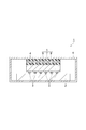
- FIG. 1 is a schematic cross-sectional view showing an electronic apparatus according to an embodiment.
- an electronic device 1 according to an embodiment includes a substrate 2, an electronic component 4 provided on the substrate 2 via a plurality of solders 3, an electromagnetic wave shielding heat radiation sheet (hereinafter simply referred to as “ 5) and a housing 6 for housing them.
- the substrate 2 may be, for example, a printed circuit board.
- the electronic component 4 may be, for example, an LSI (Large Scale Integrated Circuit), an IC (Integrated Circuit), a semiconductor package, or the like.
- the solder 3 electrically connects the wiring on the substrate 2 and the electronic component 4 to each other.
- the solder 3 may be, for example, a solder ball, and may be formed by soldering in a state where the pins of the electronic component 4 are inserted into the substrate 2.
- the housing 6 is, for example, a hollow, substantially rectangular parallelepiped box.
- the housing 6 may be made of metal or resin.
- the housing 6 may be, for example, a metal housing having electromagnetic shielding properties or a resin housing having no electromagnetic shielding properties. Since the electronic device 1 includes the heat radiation sheet 5 having electromagnetic wave shielding properties, the electronic device 1 is generated from the electronic component 4 even if the housing 6 does not have electromagnetic wave shielding properties (for example, a resin housing).
- the electromagnetic wave is suitably shielded by the heat dissipation sheet 5 and is difficult to leak out of the electronic device 1.
- the heat dissipation sheet 5 includes a conductive layer (conductive substrate) 7 and thermally conductive resin layers 8 and 9 laminated on both surfaces of the conductive layer 7, respectively.
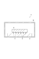
- FIG. 2 is a perspective view showing an embodiment of the heat dissipation sheet 5.
- the heat dissipation sheet 5 ⁇ / b> A according to the embodiment includes a first heat conductive resin layer 8 ⁇ / b> A, a conductive layer 7, and a second heat conductive resin layer 9 in this order.
- the first heat conductive resin layer 8A, the conductive layer 7, and the second heat conductive resin layer 9 have substantially the same planar shape (for example, a rectangular shape) so that the end faces of the respective layers are aligned with each other.
- the heat dissipation sheet 5 is configured by being laminated.
- the heat dissipation sheet 5 is disposed such that the first heat conductive resin layer 8 is in contact with the electronic component 4 and the second heat conductive resin layer 9 is in contact with the housing 6. . Thereby, the heat generated in the electronic component 4 can be released to the outside through the housing 6.
- the conductive layer 7 is preferably formed of a metal foil or a metal mesh.
- the conductive layer 7 includes, for example, at least one selected from the group consisting of aluminum, copper, silver, and gold as a metal constituting the metal foil or the metal mesh.
- the metal foil may be an aluminum foil, a copper foil, a silver foil, or a gold foil, and is preferably an aluminum foil or a copper foil from the viewpoint of obtaining a suitable specific gravity and further excellent electromagnetic wave shielding properties.
- the metal mesh may be one in which the above-described metal fibers are knitted into a mesh shape, and conductive fibers are plated, sputtered, or vapor deposited on organic fibers or inorganic fibers such as natural fibers or synthetic fibers. What was covered may be a mesh.
- natural fibers include cotton and hemp.
- synthetic fibers include polyester fibers, polyolefin fibers, and aramid fibers.
- the inorganic fiber include carbon fiber and glass fiber.
- the conductive metal may be aluminum, copper, silver or gold as described above, and may be nickel or zinc.
- the thickness of the conductive layer 7 is preferably 10 ⁇ m or more from the viewpoint of further improving the electromagnetic wave shielding properties, and preferably 300 ⁇ m or less, 200 ⁇ m or less, from the viewpoint that the flexibility and weight of the heat dissipation sheet 5 are suitable. It may be 100 ⁇ m or less, or 50 ⁇ m or less.
- the heat conductive resin layers 8 and 9 are not particularly limited, for example, they are formed of a cured product of a heat conductive resin composition containing (A) a resin component and (B) a heat conductive filler.
- the resin component is preferably a (a) silicone resin component containing a silicone resin from the viewpoint of obtaining a heat-dissipating sheet 5 having excellent flexibility and further excellent thermal conductivity (heat dissipation).
- the silicone resin component is not particularly limited, and may be a component that can be cured by a curing reaction such as peroxide crosslinking, condensation reaction crosslinking, addition reaction crosslinking, ultraviolet crosslinking, etc., preferably addition reaction crosslinking. It is a component that can be cured by a curing reaction.
- the (a) silicone resin component preferably contains an addition reaction type silicone resin, and more preferably contains a one-component addition reaction type or two-component addition reaction type silicone resin.
- the silicone resin component is preferably (a1) an organopolysiloxane having a vinyl group at least at the terminal or side chain (hereinafter also referred to as “organopolysiloxane having a vinyl group”), and (a2) at least the terminal. Or an organopolysiloxane having two or more H—Si groups in the side chain (hereinafter also referred to as “organopolysiloxane having an H—Si group”), and a two-component addition reaction type liquid silicone resin component. .
- the thermally conductive resin composition contains the thermally conductive filler at a large content of, for example, 40 to 85% by volume. Even if it exists, a highly flexible heat conductive resin layer can be obtained. Furthermore, since a large amount of thermally conductive filler can be contained, a highly thermally conductive thermally conductive resin layer can be obtained.
- (A1) is an organopolysiloxane having a vinyl group at least at the terminal or side chain, and may have either a linear structure or a branched structure.
- the organopolysiloxane having a vinyl group is, for example, a structure represented by (Si—R) in the organopolysiloxane molecule, wherein a part of the R portion is a vinyl group.
- the organopolysiloxane having a vinyl group specifically has, for example, a structural unit represented by the following formula (a1-1) or a terminal structure represented by the formula (a1-2): It's okay.
- the organopolysiloxane having a vinyl group may have, for example, a structural unit represented by the formula (a1-1) and a structural unit represented by the formula (a1-3). It may have a terminal structure represented by 2) and a structural unit represented by formula (a1-3).
- (a1) the organopolysiloxane having a vinyl group is not limited to those having these structural units or terminal structures.
- the content of the vinyl group in (a1) may be 0.01 mol% or more, 15 mol% or less or 5 mol% or less, preferably 0.01 to 15 mol%, more preferably 0.01 to 5 mol%.
- the “vinyl group content” in the present invention means the ratio (mol%) of the number of moles of vinyl groups to the total number of moles of vinyl groups and Si atoms in (a1).
- the vinyl group content is measured by the following method.
- the vinyl group content is measured by NMR. Specifically, for example, ECP-300 NMR manufactured by JEOL is used, and measurement is performed by dissolving an organopolysiloxane having a vinyl group in deuterated chloroform as a heavy solvent. Ratio of the number of moles of vinyl group when the total number of moles of vinyl group calculated from the measurement results and the number of moles of Si atoms (derived from Si—CH 3 group , H—Si group, etc.) is 100% Is the vinyl group content (mol%).
- the organopolysiloxane having a vinyl group is preferably an alkylpolysiloxane having an alkyl group in addition to the vinyl group.
- This alkyl group is preferably an alkyl group having 1 to 3 carbon atoms (for example, a methyl group, an ethyl group, etc.), and more preferably a methyl group.
- the organopolysiloxane having a vinyl group may be a methylpolysiloxane having a vinyl group at the terminal and / or side chain.
- the mass average molecular weight (also referred to as weight average molecular weight, hereinafter the same) of the organopolysiloxane having a vinyl group is preferably less than 400,000 and may be 200,000 or less, or 10,000 or more or It may be 15,000 or more, more preferably 10,000 to 200,000, still more preferably 15,000 to 200,000.
- the mass average molecular weight of the organopolysiloxane having a vinyl group is measured by the method described in Examples.
- (A2) is an organopolysiloxane having two or more H—Si groups at least at either the terminal or the side chain, and may have either a linear structure or a branched structure.
- An organopolysiloxane having an H—Si group is, for example, a structure represented by (Si—R) in the molecule of the organopolysiloxane, wherein a part of the R portion is H (hydrogen atom). is there.
- the organopolysiloxane having an H—Si group has, for example, a structural unit represented by the following formula (a2-1) or a terminal structure represented by the formula (a2-2): You can do it.
- the organopolysiloxane having an H—Si group may have, for example, a structural unit represented by the formula (a2-1) and a structural unit represented by the formula (a2-3). It may have a terminal structure represented by a2-2) and a structural unit represented by formula (a2-3).
- the (a2) organopolysiloxane having an H—Si group is not limited to those having these structural units or terminal structures.
- the content of H—Si groups in (a2) may be 0.01 mol% or more, 15 mol% or less or 5 mol% or less, preferably 0.01 to 15 mol%, more Preferably, it is 0.01 to 5 mol%.
- the “content of H—Si groups” in the present invention means the ratio (mol%) of the number of moles of H—Si groups to the number of moles of Si atoms in (a2).
- the content of H—Si groups is measured by the following method.
- the H—Si group content is measured by NMR. Specifically, for example, ECP-300 NMR manufactured by JEOL is used, and measurement is performed by dissolving an organopolysiloxane having an H—Si group in deuterated chloroform as a heavy solvent.
- the ratio of the number of moles of H—Si groups when the number of moles of Si atoms (derived from Si—CH 3 groups , H—Si groups, etc.) calculated from the measurement results is 100 mol% Content (mol%).
- the organopolysiloxane having an H—Si group is preferably an alkylpolysiloxane having an alkyl group in addition to the H—Si group.
- This alkyl group is preferably an alkyl group having 1 to 3 carbon atoms (for example, a methyl group, an ethyl group, etc.), and more preferably a methyl group.
- the organopolysiloxane having an H—Si group may be a methyl polysiloxane having two or more H—Si groups at the terminal and / or side chain.
- the weight average molecular weight of the organopolysiloxane having an H—Si group is preferably 400,000 or less, 200,000 or less, 10,000 or more, or 15,000 or more, More preferably, it is 10,000 to 200,000, and still more preferably 15,000 to 200,000.
- the mass average molecular weight of the organopolysiloxane having an H—Si group is measured by the method described in Examples.
- An organopolysiloxane having a vinyl group and (a2) an organopolysiloxane having an H—Si group have other structures having other organic groups such as a phenyl group and a trifluoropropyl group in the side chain of the polysiloxane skeleton. May further be included.
- the structural unit having other structure may be a structural unit derived from phenylmethylsiloxane or diphenylsiloxane.
- the organopolysiloxane constituting the silicone resin may be a modified organopolysiloxane having a functional group such as an epoxy group.
- the viscosity of the silicone resin component at 25 ° C. may be 100 mPa ⁇ s or more or 350 mPa ⁇ s or more, may be 2,500 mPa ⁇ s or less, or 2,000 mPa ⁇ s or less, for example, 100 to 2 , 500 mPa ⁇ s, preferably 100 to 2,000 mPa ⁇ s, more preferably 350 to 2,000 mPa ⁇ s.
- the viscosity at 25 ° C. of the silicone resin component is 100 mPa ⁇ s or more, it is advantageous in that the thermal conductive resin layer can be prevented from tearing.
- Viscosity at 25 ° C. of the silicone resin component Is 2,500 mPa ⁇ s or less, it is advantageous in that it is easy to highly fill the thermally conductive filler.
- the viscosity of the silicone resin component at 25 ° C. can be measured using, for example, a B-type viscometer “RVDVIT” manufactured by BROOKFIELD.
- the f-shaft is used as the spindle and is measured as the viscosity at 20 rpm.
- the silicone resin component preferably contains a thermosetting organopolysiloxane.
- the silicone resin component may further contain a curing agent (crosslinkable organopolysiloxane) in addition to the polyorganopolysiloxane (also referred to as base polymer or main ingredient).
- the silicone resin component may further contain an addition reaction catalyst for promoting the addition reaction.
- silicone resin component Commercially available products can be used as the (a) silicone resin component as described above.
- examples of commercially available silicone resin components include two-component addition reaction type liquid silicone rubbers such as “TSE-3062” and “X14-B8530” manufactured by Momentive, “SE-1885A / B” manufactured by Toray Dow Corning, and the like. Although it is good, it is not limited to the range of these specific commercial products.
- the resin component may further contain other resins such as an acrylic resin and an epoxy resin in addition to the above (a) silicone resin component.
- the content of the resin component (A) ((a) silicone resin component) may be 10% by volume or more or 15% by volume or more, and 65% by volume or less or 60% with respect to the total volume of the heat conductive resin layer.
- the volume may be not more than volume%, preferably 10 to 65 volume%, more preferably 15 to 60 volume%.
- the thermally conductive filler is, for example, a filler having a thermal conductivity of 10 W / m ⁇ K or more.
- the thermally conductive filler may be aluminum oxide, magnesium oxide, boron nitride, aluminum nitride, silicon nitride, silicon carbide, metallic aluminum, graphite or the like. These can be used individually by 1 type or in combination of 2 or more types as a heat conductive filler.
- the thermally conductive filler is preferably spherical (suitably sphericity is 0.85 or more).
- the heat conductive filler is preferably aluminum oxide because it exhibits higher heat conductivity and good filling into the resin.
- Aluminum oxide (hereinafter also referred to as “alumina”) may be any of flame spraying method of aluminum hydroxide powder, Bayer method, ammonium alum pyrolysis method, organoaluminum hydrolysis method, aluminum underwater discharge method, freeze drying method, etc. It may be manufactured by a method.
- the aluminum oxide is preferably produced by flame spraying of aluminum hydroxide powder from the viewpoints of particle size distribution control and particle shape control.
- the crystal structure of alumina may be either a single crystal or a polycrystal.
- the crystal phase of alumina is preferably an ⁇ phase from the viewpoint of high thermal conductivity.
- the specific gravity of alumina is preferable from the viewpoint of avoiding an increase in the proportion of voids and low crystal phases present in the alumina particles and further increasing the thermal conductivity (for example, 2.5 W / m ⁇ K or more). Is 3.7 or more.
- Alumina is preferably spherical.
- the sphericity of the alumina is from the viewpoint of suppressing the fluidity from decreasing and the filler segregating in the thermally conductive resin layer and the accompanying increase in variation in physical properties.
- Alumina having a sphericity of 0.85 or more is available as a commercial product.
- spherical alumina DAW45S trade name
- spherical alumina DAW05 trade name
- spherical alumina ASFP20 (trade name) manufactured by Denka Corporation. Etc.
- the heat conductive filler preferably has a maximum value (peak) in the particle size distribution in the range of particle size of 10 ⁇ m to 100 ⁇ m, 1 ⁇ m to less than 10 ⁇ m, or less than 1 ⁇ m.
- the particle size distribution of the heat conductive filler can be adjusted by classification and mixing operation of the heat conductive filler.
- the thermally conductive filler is preferably a thermally conductive filler (B-1) having a maximum value (peak) in a particle size range of 10 ⁇ m to 100 ⁇ m and a maximum value (peak) in a particle size range of 1 ⁇ m to less than 10 ⁇ m. And a thermally conductive filler (B-3) having a maximum value (peak) in a particle size range of less than 1 ⁇ m.
- the thermally conductive filler (B-1) may be a thermally conductive filler having an average particle size of 10 ⁇ m or more and 100 ⁇ m or less.
- the heat conductive filler (B-2) may be a heat conductive filler having an average particle diameter of 1 ⁇ m or more and less than 10 ⁇ m.
- the thermally conductive filler (B-3) may be a thermally conductive filler having an average particle size of less than 1 ⁇ m.
- the particle size distribution and average particle size of the thermally conductive filler are measured by the method described in the
- the ratio of the thermally conductive filler (B-1) is preferably 15% by volume or more, 20% by volume or more, 30% by volume or more, or 40% by volume or more with respect to the total volume of the thermally conductive filler. It may be 70% by volume or less, 60% by volume or less, or 50% by volume or less, and more preferably 20 to 60% by volume.
- the proportion of the heat conductive filler (B-2) may be 10% by volume or more, 12% by volume or more, or 20% by volume or more with respect to the total volume of the heat conductive filler, 40% by volume or less, 35 It may be not more than volume%, or not more than 30 volume%, preferably 10 to 30 volume%, more preferably 12 to 30 volume%.
- the proportion of the heat conductive filler (B-3) may be 5% by volume or more or 8% by volume or more with respect to the total volume of the heat conductive filler, and is 30% by volume or less, 25% by volume or less, 20% by volume. % Or less or 15% by volume or less, preferably 5 to 30% by volume, more preferably 8 to 20% by volume.
- the content of the heat conductive filler may be 20% by volume or more or 30% by volume or more, preferably 35% by volume or more, or 40% by volume or more with respect to the total volume of the heat conductive resin layer. It may be not more than volume% or not more than 80 volume%, preferably not more than 85 volume%, more preferably 40 to 85 volume%. When the content of the heat conductive filler is 35% by volume or more, the heat conductivity of the heat conductive resin layer is further improved. When the content of the heat conductive filler is 85% by volume or less, it is easy to avoid deterioration of the fluidity of the heat conductive resin composition, and it is easy to produce a heat conductive resin layer.
- the thermally conductive resin composition further contains a reaction retarder such as acetyl alcohols and maleates, a thickener such as Aerosil or silicone powder having a particle size of 10 to several hundred ⁇ m, a flame retardant, and a pigment. be able to.
- a reaction retarder such as acetyl alcohols and maleates
- a thickener such as Aerosil or silicone powder having a particle size of 10 to several hundred ⁇ m
- a flame retardant such as a flame retardant, and a pigment.
- the thicknesses of the first heat conductive resin layer 8 and the second heat conductive resin layer 9 may be 0.1 mm or more and 10 mm or less, respectively.
- the thermal conductivities of the first thermal conductive resin layer 8 and the second thermal conductive resin layer 9 are each preferably 0.5 W / mK or more.
- the thickness of the heat dissipating sheet 5 is preferably 0.2 mm or more, 1 mm or more or 1.5 mm or more, 15 mm or less or 12 mm or less, preferably 10 mm or less, preferably 0.2 mm to It may be 10 mm.
- the thickness of the heat radiation sheet 5 is based on the thickness after curing of the heat conductive resin composition.
- the heat dissipation sheet 5 has high thermal conductivity and has a thermal conductivity of 0.5 W / mK or more.
- the Asker C hardness of the heat dissipation sheet 5 is preferably less than 40, more preferably 35 or less, and further preferably 30 or less.
- the lower limit value of Asker C hardness is preferably 5 or more from the viewpoint of excellent handling properties when handling the heat dissipation sheet 5.
- the heat-dissipating sheet 5 is provided with a heat conductive resin composition on one surface of the conductive layer 7 to form one of the first heat conductive resin layer 8 and the second heat conductive resin layer 9.
- a step (a-2) and disposing the heat conductive resin composition on the other surface of the conductive layer 7 to form the other of the first heat conductive resin layer 8 and the second heat conductive resin layer 9
- the manufacturing method of the heat dissipation sheet 5 is such that a thermally conductive resin composition is disposed on a resin film (for example, a PET film), and the first thermally conductive resin layer 8 and the second heat On the first thermal conductive resin layer 8 or the second thermal conductive resin layer 9 formed in the step (b-1) of forming one of the conductive resin layers 9 and the step (b-1), Step (b-2) for providing (for example, laminating) the conductive layer 7 and placing the heat conductive resin composition on the conductive layer 7 provided in the step (b-2) A step (b-3) of forming the other of the resin layer 8 and the second thermally conductive resin layer 9 may be provided.
- a resin film for example, a PET film
- Step (b-2) for providing (for example, laminating) the conductive layer 7 and placing the heat conductive resin composition on the conductive layer 7 provided in the step (b-2)
- the heat conductive resin composition used in the production method of each embodiment can be obtained by a known method, for example, by mixing components (A) and (B).
- a mixer such as a roll mill, a kneader, or a Banbury mixer is used.
- the method of arranging the heat conductive resin composition is preferably a doctor blade method.
- the method may be an extrusion method, a press method, a calender roll method, or the like depending on the viscosity of the heat conductive resin composition.
- the heat conductive resin composition is heated and cured to thereby obtain the first heat conduction.
- the conductive resin layer 8 or the second thermally conductive resin layer 9 may be formed.
- Heat curing is performed using a general hot air dryer, far-infrared dryer, microwave dryer, or the like.
- the heating temperature is preferably 50 to 200 ° C. When the heating temperature is 50 ° C. or higher, crosslinking is likely to proceed sufficiently, and when it is 200 ° C. or lower, deterioration due to heating can be suppressed.
- the heat curing time is preferably 2 to 14 hours.
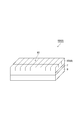
- FIG. 3 is a perspective view showing a heat dissipation sheet according to another embodiment.
- the first thermally conductive resin layer 8B has cuts 10 (a plurality of cut lines) on the surface (surface opposite to the conductive layer 7). .
- the thermal radiation sheet 5B has high flexibility and high followability in addition to high thermal conductivity.
- the notch 10 is formed in only one of the thermally conductive resin layers (the first thermally conductive resin layer 8), but in another embodiment, the thermal conductive resin layer A cut may be formed in both (the first thermally conductive resin layer 8 and the second thermally conductive resin layer 9).
- a groove (groove having a predetermined width) may be provided in the heat conductive resin layer.
- a heat conductive sheet may be provided between the electronic component and the housing. When sandwiched between them, air that cannot be discharged remains in the groove of the thermally conductive resin layer, which may increase the thermal resistance (decrease in thermal conductivity).
- the heat conductive resin layers 8 and 9 are provided with cuts so that the layers in the heat dissipation sheet 5B are stacked. The repulsive force (force in the compression direction) generated in the direction can be released in the direction perpendicular to the stacking direction, and air is difficult to enter.
- the heat dissipation sheet 5B has high followability to the shape to be applied, it is difficult to apply an excessive load to the electronic component 4 and the housing 6, and the risk of damage is reduced.
- the heat dissipation sheet 5B follows the unevenness and exhibits high adhesion.
- the heat-radiation sheet 5B is excellent in adhesiveness, since the heat generated in the electronic component 4 can be dissipated more efficiently, the heat-dissipation sheet 5B also exhibits better heat dissipation.
- the heat dissipation sheet 5B is particularly suitable for an application in which a load is applied between the electronic component 4 and the housing 6. Therefore, the heat dissipation sheet 5B is preferably a non-adhesive sheet (non-adhesive sheet including the non-adhesive thermally conductive resin layers 8 and 9) that does not have adhesiveness.
- the cut 10 is composed of one or more linear cuts (hereinafter referred to as “cut lines”).
- the cut line has such a width that a streak of cutting traces can be seen.
- the width of the score line (the length in the short direction) makes it difficult for air to enter the heat-dissipating sheet 5B, further improving the thermal conductivity (further reducing the thermal resistance), and the flexibility of the heat-dissipating sheet 5B.
- the followability can be further improved, it is preferably as small as possible, preferably 300 ⁇ m or less, more preferably less than 300 ⁇ m, still more preferably 100 ⁇ m or less, and particularly preferably 50 ⁇ m or less.
- the width of the cut line (length in the short direction) may be 2 ⁇ m or more, preferably 2 ⁇ m or more and less than 300 ⁇ m, more preferably 2 ⁇ m or more and 50 ⁇ m or less.
- the cut line may be, for example, a straight line or a curved shape such as a meandering shape or a wavy shape.
- the wave shape may be, for example, a sine wave shape, a sawtooth wave shape, a rectangular wave shape, a trapezoidal wave shape, a triangular wave shape, or the like.
- the planar shape of the cut 10 is not particularly limited.
- the planar shape of the notch 10 is a lattice shape. That is, the cut 10 shown in FIG. 3 is configured by arranging a plurality of linear cut lines in a lattice shape in plan view.
- the quadrangular planar shape constituting the lattice may be, for example, a rectangular shape or a square shape.
- planar shape of the cut may be a linear shape, a broken line shape (perforated shape), a polygonal shape, an elliptical shape, a circular shape, or the like.
- the broken line shape (perforated line shape) is, for example, in which a plurality of straight cut lines are arranged in one direction (extending direction of cut lines) at a predetermined interval (parts with cut lines and parts without cut lines) Is a shape that is repeated alternately).
- the polygonal shape is not particularly limited, and examples thereof include a triangular shape, a quadrangular shape, a pentagonal shape, a hexagonal shape, and a star shape.
- examples of the quadrangular shape include a trapezoidal shape, a rhombus shape, and a parallelogram shape.
- the planar shape of the cuts 10 is preferably linear, wavy, diamond-shaped, circular, star-shaped, and lattice-shaped, more preferably linear-shaped, diamond-shaped, and lattice-shaped, and more preferably cut-in processing. From the viewpoint of workability at the time and high followability, it is in a lattice shape (particularly, a lattice shape in which the planar shape of each square constituting the lattice is a square shape).
- the vertical cross-sectional shape of the notch 10 (the shape seen from the direction perpendicular to the stacking direction of the layers constituting the heat-dissipating sheet 5B) is not particularly limited, but for example, V-shaped, Y-shaped, l-shaped (English lowercase letters) L) shape (straight line shape), diagonal shape (slash shape), etc., and from the viewpoint that it is easy to form the cut 10 even in a state where the layers constituting the heat dissipation sheet 5B are laminated, (Lowercase letter L) (straight line).
- the cut 10 is preferably unpenetrated (not penetrating in the thickness direction (lamination direction) in the heat conductive resin layers 8 and 9).
- the length of the non-penetrating portion (the length in the thickness direction (lamination direction) of the portion where the cut is not formed in the heat conductive resin layers 8 and 9) is 0.1 mm or more, 0.15 mm or more, and 0.0.
- the ratio of the depth of the cut 10 to the thickness of the heat conductive resin layers 8 and 9 is preferably 2%. Or more, 10% or more, 20% or more, 30% or more, or 40% or more, preferably 90% or less, 80% or less, or 70% or less, preferably 2% to 90%, more preferably It may be 30% to 80%, more preferably 40% to 70%.
- the ratio is in the above range, high flexibility and high followability can be easily obtained (for example, the compressive stress (when the compression rate is 20%) can be reduced by 5% or more compared to the case where no cut is provided).
- the thermal resistance can be further reduced (thermal conductivity can be further improved).
- the notch 10 can be formed by, for example, using a cutting means and moving the cutting means in any of the thickness direction (stacking direction) and the direction perpendicular thereto, or a combination thereof.
- the cutting means can be moved in any direction (shape) such as “oblique direction” or “wavy”.
- the cutting means may be, for example, a cutting blade, laser, water jet (water cutter) or the like, and is preferably a cutting blade because the cutting line is easy to narrow and easy to process.
- the method of forming the cut 10 may be slit processing using a cutting blade, processing using a laser knife, or the like.
- the difference in Asker C hardness before and after the cut is preferably 2 or more, more preferably 5 or more.
- This “difference in Asker C before and after cutting” can be calculated by “(Asker C hardness before cutting) ⁇ (Asker C hardness after cutting)”.
- the heat conductive resin layer in which the cut is formed is brought into contact with the electronic component 4.
- the cut 10 is formed in one of the first thermal conductive resin layer 8 that contacts the electronic component 4 and the second thermal conductive resin layer 9 that contacts the housing 6, FIG. It is preferable to form the notch 10 in the 1st heat conductive resin layer 8 which contacts the electronic component 4 like the electromagnetic wave shielding heat dissipation sheet 5B shown in FIG.
- the heat radiating sheet 5B can follow the shape of the contact surface of the electronic component 4 with the first thermally conductive resin layer 8 due to high followability, and stress is applied to the heat radiating sheet 5B due to high flexibility.
- the stress can be relieved, it is difficult to damage the electronic component 4.
- the heat dissipation sheet 5B has high thermal conductivity while having high flexibility and high followability, heat generated from the electronic component 4 can be transmitted to the housing 6 particularly efficiently. Therefore, in the electronic device 1, the heat from the electronic component 4 can be efficiently released to the outside of the electronic device 1.
- the electromagnetic wave shielding heat radiation sheet 5 has an electromagnetic wave shielding property, it is possible to confine electromagnetic waves generated from the electronic component 4 and to block external electromagnetic waves.
- the electromagnetic shielding heat dissipation sheet 5 also has insulation, the spatial distance between the electronic component 4 and the housing 6 may be narrow, and the electronic device 1 can be downsized.
- the housing 6 is a metal housing, the electromagnetic wave shielding property can be further improved.
- the electromagnetic wave shielding heat radiating sheet 5 can shield the electromagnetic waves, it is necessary to use a metal housing. Instead, it is possible to contribute to further miniaturization by securing heat dissipation using a radiation fin or the like.
- FIG. 4 is a schematic cross-sectional view showing a conventional electronic device.
- the conventional electronic device 11 is not provided with an electromagnetic wave shielding heat dissipating sheet, and the housing 16 blocks electromagnetic waves generated from the electronic component 4 and heat generated from the electronic component 4.
- the casing 16 is made of metal from the viewpoint of obtaining electromagnetic wave shielding properties and heat dissipation.
- the electronic component 4 and the casing 16 are secured. And a spatial distance is required. Therefore, it is difficult to reduce the size of the conventional electronic device 11.
- the electronic device 1 including the electromagnetic wave shielding heat dissipation sheet 5 of the present embodiment can suppress malfunction and noise due to electromagnetic waves. Moreover, it can provide as the electronic component 4 which can reduce the lifetime reduction of the electronic component 4 by a temperature rise, a distortion
- the electromagnetic wave shielding heat radiation sheet 5B has both electromagnetic wave shielding properties and thermal conductivity, has a reduced compressive load (stress), and has high followability to an application target such as the electronic component 4 or the like. Can be provided. Further, in the heat dissipating sheet 5B, since the notch 10 is provided instead of the so-called groove, air does not remain, the followability to the application target of the electronic component 4 and the like is high, and the adhesiveness is also high. Is also expensive.
- the heat dissipation sheet 5B is particularly suitable as an electromagnetic shielding material for electronic parts and a heat dissipation member.
- the heat radiation sheet 5B is preferably used as a heat radiating member for an electronic component that requires adhesion between the heat generating surface of the semiconductor element and the heat radiating surface such as a heat radiating fin.
- the heat radiating sheet 5B is suitably used for electromagnetic shielding materials and heat conducting members such as industrial members, and particularly suitable as a high heat conducting sheet and heat radiating member having high flexibility that can reduce compressive stress during mounting. It is used.
- thermoly conductive resin composition was prepared by mixing the conductive filler at a blending ratio (volume%) shown in Tables 1 to 3. The total amount of component (A) and component (B) was 100% by volume.
- the mass average molecular weight of the polyorganosiloxane was a value in terms of polystyrene determined from the results of gel permeation chromatography analysis. Separation was performed using a non-aqueous porous gel (polystyrene-dimethylbenzene copolymer), toluene was used as the mobile phase, and a differential refractometer (RI) was used for detection.
- RI differential refractometer
- thermally conductive filler The following aluminum oxide (alumina) was used as the thermally conductive filler.
- total filler volume%) of the thermally conductive filler is the total amount of each spherical filler and each crystalline alumina used.
- the average particle diameter of the thermally conductive filler was measured using “Laser Diffraction Particle Size Analyzer SALD-20” manufactured by Shimadzu Corporation.
- SALD-20 “Laser Diffraction Particle Size Analyzer SALD-20” manufactured by Shimadzu Corporation.
- 5 g of 50 cc pure water and a thermally conductive filler powder to be measured were added to a glass beaker, stirred using a spatula, and then subjected to dispersion treatment for 10 minutes with an ultrasonic cleaner.
- the solution of the thermally conductive filler powder that had been subjected to the dispersion treatment was added drop by drop to the sampler portion of the apparatus using a dropper, and measurement was performed when the absorbance was stable.
- the particle size distribution is calculated from the data of the light intensity distribution of the diffracted / scattered light by the particles detected by the sensor.
- the average particle size is obtained by multiplying the value of the measured particle size by the relative particle amount (difference%) and dividing by the total relative particle amount (100%).
- an average particle diameter is an average diameter of particle
- D50 becomes a particle size with the largest appearance rate.
- the obtained heat conductive resin composition was formed on one surface of each conductive layer shown in Tables 1 and 2 with a thickness shown in Tables 1 and 2. After placing so as to obtain a conductive resin layer, heat curing was performed at 110 ° C. for 8 hours. Then, after arrange
- notches were formed in one or both of the heat conductive resin layers in the heat dissipation sheet obtained in Example 8. More specifically, using a cutting blade, linear cutting lines were made in two directions perpendicular to one or both of the thermally conductive resin layers to form a grid-shaped cutting.
- the width of the score line (the length in the short direction) is 50 ⁇ m or less
- the plane shape of each quadrangle constituting the lattice is 1.5 mm ⁇ 1.5 mm square
- the number of quadrilaterals constituting the lattice is 15 mm.
- the ratio of the depth to the depth of cut (length in the thickness direction) and the thickness of the heat conductive resin layer is as shown in Table 3.
- the electromagnetic shielding effect at 1 MHz was measured by the KEC method. If the shielding effect is 10 dB or more, it can be said that the electromagnetic wave shielding property is excellent, and if it is 20 dB or more, it can be said that the shielding effect is particularly excellent.
- Asker C hardness> Asker C hardness was measured by “Asker Rubber Hardness Tester C Type” manufactured by Kobunshi Keiki Co., Ltd. If the Asker C hardness is less than 40, the heat radiating sheet has high flexibility, and if the Asker C hardness is 15 or less, it can be said that the heat radiating sheet has particularly high flexibility.
- the electromagnetic shielding heat dissipation sheet of the present invention has high electromagnetic shielding properties and thermal conductivity, and also reduces the compressive load (compressive stress) when the sheet is used, and has high followability to the application target.
- the electromagnetic wave shielding heat dissipation sheet of the present invention can be suitably applied to an electromagnetic wave shield and a heat dissipation member for electronic components.
- an electromagnetic wave shielding heat dissipation sheet suitable for electric parts related to automobiles such as car navigation systems, radios, and automatic driving related devices).
Landscapes
- Engineering & Computer Science (AREA)
- Microelectronics & Electronic Packaging (AREA)
- Physics & Mathematics (AREA)
- Condensed Matter Physics & Semiconductors (AREA)
- General Physics & Mathematics (AREA)
- Computer Hardware Design (AREA)
- Power Engineering (AREA)
- Chemical & Material Sciences (AREA)
- Materials Engineering (AREA)
- Thermal Sciences (AREA)
- Cooling Or The Like Of Semiconductors Or Solid State Devices (AREA)
- Laminated Bodies (AREA)
- Shielding Devices Or Components To Electric Or Magnetic Fields (AREA)
- Cooling Or The Like Of Electrical Apparatus (AREA)
- Compositions Of Macromolecular Compounds (AREA)
Abstract
Un appareil électronique selon un aspect de la présente invention est pourvu d'un composant électronique, d'une feuille de dissipation de chaleur de protection contre les ondes électromagnétiques, et d'un boîtier qui reçoit le composant électronique et la feuille de dissipation de chaleur de protection contre les ondes électromagnétiques, la feuille de dissipation de chaleur de protection contre les ondes électromagnétiques étant pourvue d'une première couche de résine thermoconductrice, une couche conductrice, et une seconde couche de résine conductrice de chaleur dans cet ordre, et est disposée de telle sorte que la première couche de résine thermoconductrice est en contact avec le composant électromagnétique et que la seconde couche de résine conductrice de chaleur est en contact avec le boîtier.
Priority Applications (1)
| Application Number | Priority Date | Filing Date | Title |
|---|---|---|---|
| JP2020511834A JPWO2019230607A1 (ja) | 2018-05-29 | 2019-05-24 | 電子機器及び電磁波シールド性放熱シート |
Applications Claiming Priority (2)
| Application Number | Priority Date | Filing Date | Title |
|---|---|---|---|
| JP2018-102144 | 2018-05-29 | ||
| JP2018102144 | 2018-05-29 |
Publications (1)
| Publication Number | Publication Date |
|---|---|
| WO2019230607A1 true WO2019230607A1 (fr) | 2019-12-05 |
Family
ID=68697002
Family Applications (1)
| Application Number | Title | Priority Date | Filing Date |
|---|---|---|---|
| PCT/JP2019/020743 WO2019230607A1 (fr) | 2018-05-29 | 2019-05-24 | Appareil électronique et feuille de dissipation de chaleur deprotection contre les ondes électromagnétiques |
Country Status (3)
| Country | Link |
|---|---|
| JP (3) | JPWO2019230607A1 (fr) |
| TW (1) | TW202003236A (fr) |
| WO (1) | WO2019230607A1 (fr) |
Cited By (4)
| Publication number | Priority date | Publication date | Assignee | Title |
|---|---|---|---|---|
| CN111136851A (zh) * | 2019-12-31 | 2020-05-12 | 九牧厨卫股份有限公司 | 一种高强度耐腐蚀制品及其制备方法 |
| CN111315197A (zh) * | 2020-04-02 | 2020-06-19 | 深圳市龙航科技有限公司 | 一种带有散热结构的车载导航仪 |
| JP2021163789A (ja) * | 2020-03-30 | 2021-10-11 | Jx金属株式会社 | 電磁波シールド材 |
| CN114628368A (zh) * | 2022-03-10 | 2022-06-14 | 深圳市赛元微电子有限公司 | 一种芯片电路模块的电磁屏蔽装置 |
Families Citing this family (2)
| Publication number | Priority date | Publication date | Assignee | Title |
|---|---|---|---|---|
| JPWO2023008538A1 (fr) * | 2021-07-29 | 2023-02-02 | ||
| JP2023087808A (ja) * | 2021-12-14 | 2023-06-26 | オムロン株式会社 | 実装基板、及び実装基板を搭載した電気機器 |
Citations (5)
| Publication number | Priority date | Publication date | Assignee | Title |
|---|---|---|---|---|
| JPH11317591A (ja) * | 1998-05-07 | 1999-11-16 | Porimatec Kk | 熱伝導性電磁波シールドシート |
| JP2001189582A (ja) * | 1999-12-28 | 2001-07-10 | Kitagawa Ind Co Ltd | 電子部品用放熱体 |
| JP2003224386A (ja) * | 2002-01-31 | 2003-08-08 | Toyota Motor Corp | 自動車用電子装置及び自動車用電子装置用ハウジング |
| JP2015153743A (ja) * | 2014-02-19 | 2015-08-24 | 日立建機株式会社 | 蓄電装置及びこれを搭載した作業機械 |
| JP2016186972A (ja) * | 2015-03-27 | 2016-10-27 | 東レ株式会社 | 電磁波シールドシート、それを硬化させてなる硬化膜、金属箔積層電磁波シールドシートの製造方法、積層体および半導体装置 |
Family Cites Families (9)
| Publication number | Priority date | Publication date | Assignee | Title |
|---|---|---|---|---|
| JPH02102452U (fr) * | 1989-02-02 | 1990-08-15 | ||
| JP3498823B2 (ja) * | 1996-04-30 | 2004-02-23 | 電気化学工業株式会社 | 放熱スペーサーおよびその用途 |
| JP3372462B2 (ja) * | 1997-11-27 | 2003-02-04 | 電気化学工業株式会社 | ゴムシートの製造方法 |
| JP2002194306A (ja) * | 2000-12-26 | 2002-07-10 | Sekisui Chem Co Ltd | 熱伝導性シート |
| JP2005228955A (ja) * | 2004-02-13 | 2005-08-25 | Denki Kagaku Kogyo Kk | 放熱部材、その製造方法及び用途 |
| JP4798629B2 (ja) * | 2006-11-13 | 2011-10-19 | 北川工業株式会社 | 熱伝導性電磁波シールドシート及び電磁波シールド構造 |
| JP2012059811A (ja) * | 2010-09-07 | 2012-03-22 | Mochida Shoko Kk | 放熱シート |
| JP5749536B2 (ja) * | 2011-03-28 | 2015-07-15 | 電気化学工業株式会社 | 熱伝導性成形体とその用途 |
| JP2017112144A (ja) * | 2015-12-14 | 2017-06-22 | 富士通株式会社 | 電子装置、熱伝導部材、及び電子装置の製造方法 |
-
2019
- 2019-05-24 WO PCT/JP2019/020743 patent/WO2019230607A1/fr active Application Filing
- 2019-05-24 JP JP2020511834A patent/JPWO2019230607A1/ja active Pending
- 2019-05-29 TW TW108118482A patent/TW202003236A/zh unknown
-
2020
- 2020-08-31 JP JP2020145961A patent/JP2021005715A/ja active Pending
-
2021
- 2021-07-05 JP JP2021111563A patent/JP7351874B2/ja active Active
Patent Citations (5)
| Publication number | Priority date | Publication date | Assignee | Title |
|---|---|---|---|---|
| JPH11317591A (ja) * | 1998-05-07 | 1999-11-16 | Porimatec Kk | 熱伝導性電磁波シールドシート |
| JP2001189582A (ja) * | 1999-12-28 | 2001-07-10 | Kitagawa Ind Co Ltd | 電子部品用放熱体 |
| JP2003224386A (ja) * | 2002-01-31 | 2003-08-08 | Toyota Motor Corp | 自動車用電子装置及び自動車用電子装置用ハウジング |
| JP2015153743A (ja) * | 2014-02-19 | 2015-08-24 | 日立建機株式会社 | 蓄電装置及びこれを搭載した作業機械 |
| JP2016186972A (ja) * | 2015-03-27 | 2016-10-27 | 東レ株式会社 | 電磁波シールドシート、それを硬化させてなる硬化膜、金属箔積層電磁波シールドシートの製造方法、積層体および半導体装置 |
Cited By (5)
| Publication number | Priority date | Publication date | Assignee | Title |
|---|---|---|---|---|
| CN111136851A (zh) * | 2019-12-31 | 2020-05-12 | 九牧厨卫股份有限公司 | 一种高强度耐腐蚀制品及其制备方法 |
| CN111136851B (zh) * | 2019-12-31 | 2021-10-26 | 九牧厨卫股份有限公司 | 一种高强度耐腐蚀制品及其制备方法 |
| JP2021163789A (ja) * | 2020-03-30 | 2021-10-11 | Jx金属株式会社 | 電磁波シールド材 |
| CN111315197A (zh) * | 2020-04-02 | 2020-06-19 | 深圳市龙航科技有限公司 | 一种带有散热结构的车载导航仪 |
| CN114628368A (zh) * | 2022-03-10 | 2022-06-14 | 深圳市赛元微电子有限公司 | 一种芯片电路模块的电磁屏蔽装置 |
Also Published As
| Publication number | Publication date |
|---|---|
| JP2021177561A (ja) | 2021-11-11 |
| JPWO2019230607A1 (ja) | 2020-07-02 |
| TW202003236A (zh) | 2020-01-16 |
| JP7351874B2 (ja) | 2023-09-27 |
| JP2021005715A (ja) | 2021-01-14 |
Similar Documents
| Publication | Publication Date | Title |
|---|---|---|
| WO2019230607A1 (fr) | Appareil électronique et feuille de dissipation de chaleur deprotection contre les ondes électromagnétiques | |
| JP5407120B2 (ja) | 熱伝導シート、その製造方法およびこれを用いた放熱装置 | |
| JP7387823B2 (ja) | 熱伝導性シート及びその製造方法 | |
| JP5698932B2 (ja) | 熱伝導性シート | |
| JP7389014B2 (ja) | 絶縁放熱シート | |
| CN111725162A (zh) | 导热片、导热片的制造方法、放热部件和半导体装置 | |
| CN114555714B (zh) | 导热片及其制造方法 | |
| JP6634717B2 (ja) | 熱伝導性シート、熱伝導性シートの硬化物および半導体装置 | |
| JP6657616B2 (ja) | 熱伝導性シート、熱伝導性シートの硬化物および半導体装置 | |
| CN112955506B (zh) | 导热性组合物、导热性构件、导热性构件的制造方法、散热结构、发热复合构件、散热复合构件 | |
| JP5454300B2 (ja) | 熱伝導シート、その製造方法及びこれを用いた放熱装置 | |
| JP2017059704A (ja) | 熱伝導組成物、熱伝導シート、熱伝導シートの製造方法、及び部材 | |
| JP2011230472A (ja) | 絶縁性の高い熱伝導シート及びこれを用いた放熱装置 | |
| CN106133900B (zh) | 导热片和半导体装置 | |
| JP2009076657A (ja) | 熱伝導シート | |
| JP7007161B2 (ja) | 樹脂組成物及び積層体 | |
| JP7473103B2 (ja) | 熱伝導性シート及びその製造方法 | |
| US20240124758A1 (en) | Heat-conductive sheet, heat-conductive sheet production method, and electronic equipment | |
| JP2024045039A (ja) | 樹脂シート | |
| JP2019089956A (ja) | 樹脂組成物及び積層体 | |
| JP2008004838A (ja) | 熱伝導性電気絶縁性回路基板 |
Legal Events
| Date | Code | Title | Description |
|---|---|---|---|
| 121 | Ep: the epo has been informed by wipo that ep was designated in this application |
Ref document number: 19811743 Country of ref document: EP Kind code of ref document: A1 |
|
| ENP | Entry into the national phase |
Ref document number: 2020511834 Country of ref document: JP Kind code of ref document: A |
|
| NENP | Non-entry into the national phase |
Ref country code: DE |
|
| 122 | Ep: pct application non-entry in european phase |
Ref document number: 19811743 Country of ref document: EP Kind code of ref document: A1 |