WO2019230607A1 - Electronic apparatus and electromagnetic wave-shielding heat dissipation sheet - Google Patents
Electronic apparatus and electromagnetic wave-shielding heat dissipation sheet Download PDFInfo
- Publication number
- WO2019230607A1 WO2019230607A1 PCT/JP2019/020743 JP2019020743W WO2019230607A1 WO 2019230607 A1 WO2019230607 A1 WO 2019230607A1 JP 2019020743 W JP2019020743 W JP 2019020743W WO 2019230607 A1 WO2019230607 A1 WO 2019230607A1
- Authority
- WO
- WIPO (PCT)
- Prior art keywords
- heat
- resin layer
- conductive resin
- heat conductive
- heat dissipation
- Prior art date
Links
Images

Classifications
-
- B—PERFORMING OPERATIONS; TRANSPORTING
- B32—LAYERED PRODUCTS
- B32B—LAYERED PRODUCTS, i.e. PRODUCTS BUILT-UP OF STRATA OF FLAT OR NON-FLAT, e.g. CELLULAR OR HONEYCOMB, FORM
- B32B15/00—Layered products comprising a layer of metal
- B32B15/04—Layered products comprising a layer of metal comprising metal as the main or only constituent of a layer, which is next to another layer of the same or of a different material
- B32B15/08—Layered products comprising a layer of metal comprising metal as the main or only constituent of a layer, which is next to another layer of the same or of a different material of synthetic resin
-
- B—PERFORMING OPERATIONS; TRANSPORTING
- B32—LAYERED PRODUCTS
- B32B—LAYERED PRODUCTS, i.e. PRODUCTS BUILT-UP OF STRATA OF FLAT OR NON-FLAT, e.g. CELLULAR OR HONEYCOMB, FORM
- B32B27/00—Layered products comprising a layer of synthetic resin
-
- B—PERFORMING OPERATIONS; TRANSPORTING
- B32—LAYERED PRODUCTS
- B32B—LAYERED PRODUCTS, i.e. PRODUCTS BUILT-UP OF STRATA OF FLAT OR NON-FLAT, e.g. CELLULAR OR HONEYCOMB, FORM
- B32B27/00—Layered products comprising a layer of synthetic resin
- B32B27/06—Layered products comprising a layer of synthetic resin as the main or only constituent of a layer, which is next to another layer of the same or of a different material
-
- B—PERFORMING OPERATIONS; TRANSPORTING
- B32—LAYERED PRODUCTS
- B32B—LAYERED PRODUCTS, i.e. PRODUCTS BUILT-UP OF STRATA OF FLAT OR NON-FLAT, e.g. CELLULAR OR HONEYCOMB, FORM
- B32B27/00—Layered products comprising a layer of synthetic resin
- B32B27/18—Layered products comprising a layer of synthetic resin characterised by the use of special additives
- B32B27/20—Layered products comprising a layer of synthetic resin characterised by the use of special additives using fillers, pigments, thixotroping agents
-
- H—ELECTRICITY
- H01—ELECTRIC ELEMENTS
- H01L—SEMICONDUCTOR DEVICES NOT COVERED BY CLASS H10
- H01L23/00—Details of semiconductor or other solid state devices
-
- H—ELECTRICITY
- H01—ELECTRIC ELEMENTS
- H01L—SEMICONDUCTOR DEVICES NOT COVERED BY CLASS H10
- H01L23/00—Details of semiconductor or other solid state devices
- H01L23/34—Arrangements for cooling, heating, ventilating or temperature compensation ; Temperature sensing arrangements
- H01L23/36—Selection of materials, or shaping, to facilitate cooling or heating, e.g. heatsinks
-
- H—ELECTRICITY
- H05—ELECTRIC TECHNIQUES NOT OTHERWISE PROVIDED FOR
- H05K—PRINTED CIRCUITS; CASINGS OR CONSTRUCTIONAL DETAILS OF ELECTRIC APPARATUS; MANUFACTURE OF ASSEMBLAGES OF ELECTRICAL COMPONENTS
- H05K7/00—Constructional details common to different types of electric apparatus
- H05K7/20—Modifications to facilitate cooling, ventilating, or heating
-
- H—ELECTRICITY
- H05—ELECTRIC TECHNIQUES NOT OTHERWISE PROVIDED FOR
- H05K—PRINTED CIRCUITS; CASINGS OR CONSTRUCTIONAL DETAILS OF ELECTRIC APPARATUS; MANUFACTURE OF ASSEMBLAGES OF ELECTRICAL COMPONENTS
- H05K9/00—Screening of apparatus or components against electric or magnetic fields
-
- H—ELECTRICITY
- H01—ELECTRIC ELEMENTS
- H01L—SEMICONDUCTOR DEVICES NOT COVERED BY CLASS H10
- H01L2224/00—Indexing scheme for arrangements for connecting or disconnecting semiconductor or solid-state bodies and methods related thereto as covered by H01L24/00
- H01L2224/01—Means for bonding being attached to, or being formed on, the surface to be connected, e.g. chip-to-package, die-attach, "first-level" interconnects; Manufacturing methods related thereto
- H01L2224/10—Bump connectors; Manufacturing methods related thereto
- H01L2224/15—Structure, shape, material or disposition of the bump connectors after the connecting process
- H01L2224/16—Structure, shape, material or disposition of the bump connectors after the connecting process of an individual bump connector
- H01L2224/161—Disposition
- H01L2224/16151—Disposition the bump connector connecting between a semiconductor or solid-state body and an item not being a semiconductor or solid-state body, e.g. chip-to-substrate, chip-to-passive
- H01L2224/16221—Disposition the bump connector connecting between a semiconductor or solid-state body and an item not being a semiconductor or solid-state body, e.g. chip-to-substrate, chip-to-passive the body and the item being stacked
- H01L2224/16225—Disposition the bump connector connecting between a semiconductor or solid-state body and an item not being a semiconductor or solid-state body, e.g. chip-to-substrate, chip-to-passive the body and the item being stacked the item being non-metallic, e.g. insulating substrate with or without metallisation
-
- H—ELECTRICITY
- H01—ELECTRIC ELEMENTS
- H01L—SEMICONDUCTOR DEVICES NOT COVERED BY CLASS H10
- H01L2224/00—Indexing scheme for arrangements for connecting or disconnecting semiconductor or solid-state bodies and methods related thereto as covered by H01L24/00
- H01L2224/01—Means for bonding being attached to, or being formed on, the surface to be connected, e.g. chip-to-package, die-attach, "first-level" interconnects; Manufacturing methods related thereto
- H01L2224/26—Layer connectors, e.g. plate connectors, solder or adhesive layers; Manufacturing methods related thereto
- H01L2224/2612—Auxiliary members for layer connectors, e.g. spacers
-
- H—ELECTRICITY
- H01—ELECTRIC ELEMENTS
- H01L—SEMICONDUCTOR DEVICES NOT COVERED BY CLASS H10
- H01L2224/00—Indexing scheme for arrangements for connecting or disconnecting semiconductor or solid-state bodies and methods related thereto as covered by H01L24/00
- H01L2224/73—Means for bonding being of different types provided for in two or more of groups H01L2224/10, H01L2224/18, H01L2224/26, H01L2224/34, H01L2224/42, H01L2224/50, H01L2224/63, H01L2224/71
- H01L2224/732—Location after the connecting process
- H01L2224/73251—Location after the connecting process on different surfaces
- H01L2224/73253—Bump and layer connectors
Definitions
- the present invention relates to an electronic device and an electromagnetic wave shielding heat dissipation sheet.
- the sheet-like electromagnetic shielding material described in Patent Document 1 does not have heat dissipation properties, and it is necessary to separately provide a heat dissipation member in the electronic device for heat dissipation. In this case, since the number of members increases, it is difficult to reduce the size of the electronic device.
- an object of the present invention is to reduce the size of an electronic device while imparting electromagnetic shielding properties and heat dissipation to the electronic device.
- the present inventors have used a sheet in which a heat conductive resin layer is laminated on both sides of a conductive layer.
- One heat conductive resin layer is an electronic component and the other heat conductive resin layer is a housing. It has been found that the electronic device can be reduced in size while providing electromagnetic shielding properties and heat dissipation properties to the electronic device by arranging them so as to be in contact with each other.
- the present invention can provide the following in some aspects.
- Electronic equipment that is arranged.
- the electronic device according to [1], wherein the conductive layer is formed of a metal foil or a metal mesh.
- the conductive layer includes at least one selected from the group consisting of aluminum, copper, silver, and gold.
- each of the first heat conductive resin layer and the second heat conductive resin layer includes a silicone resin and a heat conductive filler.
- the content of the heat conductive filler is 40 to 85% by volume with respect to each of the first heat conductive resin layer and the second heat conductive resin layer.
- a plurality of cuts are formed in at least one of the first heat conductive resin layer and the second heat conductive resin layer.
- An electromagnetic wave shielding heat dissipating sheet comprising a first heat conductive resin layer, a conductive layer, and a second heat conductive resin layer in this order.
- Heat dissipation sheet [11] The electromagnetic wave shield according to [10], wherein the content of the heat conductive filler is 40 to 85% by volume with respect to each of the first heat conductive resin layer and the second heat conductive resin layer. Heat dissipation sheet. [12] The electromagnetic wave shielding heat dissipation according to any one of [7] to [11], wherein a plurality of cuts are formed in at least one of the first thermal conductive resin layer and the second thermal conductive resin layer. Sheet.
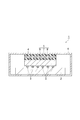
- FIG. 1 is a schematic cross-sectional view showing an electronic apparatus according to an embodiment.
- an electronic device 1 according to an embodiment includes a substrate 2, an electronic component 4 provided on the substrate 2 via a plurality of solders 3, an electromagnetic wave shielding heat radiation sheet (hereinafter simply referred to as “ 5) and a housing 6 for housing them.
- the substrate 2 may be, for example, a printed circuit board.
- the electronic component 4 may be, for example, an LSI (Large Scale Integrated Circuit), an IC (Integrated Circuit), a semiconductor package, or the like.
- the solder 3 electrically connects the wiring on the substrate 2 and the electronic component 4 to each other.
- the solder 3 may be, for example, a solder ball, and may be formed by soldering in a state where the pins of the electronic component 4 are inserted into the substrate 2.
- the housing 6 is, for example, a hollow, substantially rectangular parallelepiped box.
- the housing 6 may be made of metal or resin.
- the housing 6 may be, for example, a metal housing having electromagnetic shielding properties or a resin housing having no electromagnetic shielding properties. Since the electronic device 1 includes the heat radiation sheet 5 having electromagnetic wave shielding properties, the electronic device 1 is generated from the electronic component 4 even if the housing 6 does not have electromagnetic wave shielding properties (for example, a resin housing).
- the electromagnetic wave is suitably shielded by the heat dissipation sheet 5 and is difficult to leak out of the electronic device 1.
- the heat dissipation sheet 5 includes a conductive layer (conductive substrate) 7 and thermally conductive resin layers 8 and 9 laminated on both surfaces of the conductive layer 7, respectively.
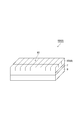
- FIG. 2 is a perspective view showing an embodiment of the heat dissipation sheet 5.
- the heat dissipation sheet 5 ⁇ / b> A according to the embodiment includes a first heat conductive resin layer 8 ⁇ / b> A, a conductive layer 7, and a second heat conductive resin layer 9 in this order.
- the first heat conductive resin layer 8A, the conductive layer 7, and the second heat conductive resin layer 9 have substantially the same planar shape (for example, a rectangular shape) so that the end faces of the respective layers are aligned with each other.
- the heat dissipation sheet 5 is configured by being laminated.
- the heat dissipation sheet 5 is disposed such that the first heat conductive resin layer 8 is in contact with the electronic component 4 and the second heat conductive resin layer 9 is in contact with the housing 6. . Thereby, the heat generated in the electronic component 4 can be released to the outside through the housing 6.
- the conductive layer 7 is preferably formed of a metal foil or a metal mesh.
- the conductive layer 7 includes, for example, at least one selected from the group consisting of aluminum, copper, silver, and gold as a metal constituting the metal foil or the metal mesh.
- the metal foil may be an aluminum foil, a copper foil, a silver foil, or a gold foil, and is preferably an aluminum foil or a copper foil from the viewpoint of obtaining a suitable specific gravity and further excellent electromagnetic wave shielding properties.
- the metal mesh may be one in which the above-described metal fibers are knitted into a mesh shape, and conductive fibers are plated, sputtered, or vapor deposited on organic fibers or inorganic fibers such as natural fibers or synthetic fibers. What was covered may be a mesh.
- natural fibers include cotton and hemp.
- synthetic fibers include polyester fibers, polyolefin fibers, and aramid fibers.
- the inorganic fiber include carbon fiber and glass fiber.
- the conductive metal may be aluminum, copper, silver or gold as described above, and may be nickel or zinc.
- the thickness of the conductive layer 7 is preferably 10 ⁇ m or more from the viewpoint of further improving the electromagnetic wave shielding properties, and preferably 300 ⁇ m or less, 200 ⁇ m or less, from the viewpoint that the flexibility and weight of the heat dissipation sheet 5 are suitable. It may be 100 ⁇ m or less, or 50 ⁇ m or less.
- the heat conductive resin layers 8 and 9 are not particularly limited, for example, they are formed of a cured product of a heat conductive resin composition containing (A) a resin component and (B) a heat conductive filler.
- the resin component is preferably a (a) silicone resin component containing a silicone resin from the viewpoint of obtaining a heat-dissipating sheet 5 having excellent flexibility and further excellent thermal conductivity (heat dissipation).
- the silicone resin component is not particularly limited, and may be a component that can be cured by a curing reaction such as peroxide crosslinking, condensation reaction crosslinking, addition reaction crosslinking, ultraviolet crosslinking, etc., preferably addition reaction crosslinking. It is a component that can be cured by a curing reaction.
- the (a) silicone resin component preferably contains an addition reaction type silicone resin, and more preferably contains a one-component addition reaction type or two-component addition reaction type silicone resin.
- the silicone resin component is preferably (a1) an organopolysiloxane having a vinyl group at least at the terminal or side chain (hereinafter also referred to as “organopolysiloxane having a vinyl group”), and (a2) at least the terminal. Or an organopolysiloxane having two or more H—Si groups in the side chain (hereinafter also referred to as “organopolysiloxane having an H—Si group”), and a two-component addition reaction type liquid silicone resin component. .
- the thermally conductive resin composition contains the thermally conductive filler at a large content of, for example, 40 to 85% by volume. Even if it exists, a highly flexible heat conductive resin layer can be obtained. Furthermore, since a large amount of thermally conductive filler can be contained, a highly thermally conductive thermally conductive resin layer can be obtained.
- (A1) is an organopolysiloxane having a vinyl group at least at the terminal or side chain, and may have either a linear structure or a branched structure.
- the organopolysiloxane having a vinyl group is, for example, a structure represented by (Si—R) in the organopolysiloxane molecule, wherein a part of the R portion is a vinyl group.
- the organopolysiloxane having a vinyl group specifically has, for example, a structural unit represented by the following formula (a1-1) or a terminal structure represented by the formula (a1-2): It's okay.
- the organopolysiloxane having a vinyl group may have, for example, a structural unit represented by the formula (a1-1) and a structural unit represented by the formula (a1-3). It may have a terminal structure represented by 2) and a structural unit represented by formula (a1-3).
- (a1) the organopolysiloxane having a vinyl group is not limited to those having these structural units or terminal structures.
- the content of the vinyl group in (a1) may be 0.01 mol% or more, 15 mol% or less or 5 mol% or less, preferably 0.01 to 15 mol%, more preferably 0.01 to 5 mol%.
- the “vinyl group content” in the present invention means the ratio (mol%) of the number of moles of vinyl groups to the total number of moles of vinyl groups and Si atoms in (a1).
- the vinyl group content is measured by the following method.
- the vinyl group content is measured by NMR. Specifically, for example, ECP-300 NMR manufactured by JEOL is used, and measurement is performed by dissolving an organopolysiloxane having a vinyl group in deuterated chloroform as a heavy solvent. Ratio of the number of moles of vinyl group when the total number of moles of vinyl group calculated from the measurement results and the number of moles of Si atoms (derived from Si—CH 3 group , H—Si group, etc.) is 100% Is the vinyl group content (mol%).
- the organopolysiloxane having a vinyl group is preferably an alkylpolysiloxane having an alkyl group in addition to the vinyl group.
- This alkyl group is preferably an alkyl group having 1 to 3 carbon atoms (for example, a methyl group, an ethyl group, etc.), and more preferably a methyl group.
- the organopolysiloxane having a vinyl group may be a methylpolysiloxane having a vinyl group at the terminal and / or side chain.
- the mass average molecular weight (also referred to as weight average molecular weight, hereinafter the same) of the organopolysiloxane having a vinyl group is preferably less than 400,000 and may be 200,000 or less, or 10,000 or more or It may be 15,000 or more, more preferably 10,000 to 200,000, still more preferably 15,000 to 200,000.
- the mass average molecular weight of the organopolysiloxane having a vinyl group is measured by the method described in Examples.
- (A2) is an organopolysiloxane having two or more H—Si groups at least at either the terminal or the side chain, and may have either a linear structure or a branched structure.
- An organopolysiloxane having an H—Si group is, for example, a structure represented by (Si—R) in the molecule of the organopolysiloxane, wherein a part of the R portion is H (hydrogen atom). is there.
- the organopolysiloxane having an H—Si group has, for example, a structural unit represented by the following formula (a2-1) or a terminal structure represented by the formula (a2-2): You can do it.
- the organopolysiloxane having an H—Si group may have, for example, a structural unit represented by the formula (a2-1) and a structural unit represented by the formula (a2-3). It may have a terminal structure represented by a2-2) and a structural unit represented by formula (a2-3).
- the (a2) organopolysiloxane having an H—Si group is not limited to those having these structural units or terminal structures.
- the content of H—Si groups in (a2) may be 0.01 mol% or more, 15 mol% or less or 5 mol% or less, preferably 0.01 to 15 mol%, more Preferably, it is 0.01 to 5 mol%.
- the “content of H—Si groups” in the present invention means the ratio (mol%) of the number of moles of H—Si groups to the number of moles of Si atoms in (a2).
- the content of H—Si groups is measured by the following method.
- the H—Si group content is measured by NMR. Specifically, for example, ECP-300 NMR manufactured by JEOL is used, and measurement is performed by dissolving an organopolysiloxane having an H—Si group in deuterated chloroform as a heavy solvent.
- the ratio of the number of moles of H—Si groups when the number of moles of Si atoms (derived from Si—CH 3 groups , H—Si groups, etc.) calculated from the measurement results is 100 mol% Content (mol%).
- the organopolysiloxane having an H—Si group is preferably an alkylpolysiloxane having an alkyl group in addition to the H—Si group.
- This alkyl group is preferably an alkyl group having 1 to 3 carbon atoms (for example, a methyl group, an ethyl group, etc.), and more preferably a methyl group.
- the organopolysiloxane having an H—Si group may be a methyl polysiloxane having two or more H—Si groups at the terminal and / or side chain.
- the weight average molecular weight of the organopolysiloxane having an H—Si group is preferably 400,000 or less, 200,000 or less, 10,000 or more, or 15,000 or more, More preferably, it is 10,000 to 200,000, and still more preferably 15,000 to 200,000.
- the mass average molecular weight of the organopolysiloxane having an H—Si group is measured by the method described in Examples.
- An organopolysiloxane having a vinyl group and (a2) an organopolysiloxane having an H—Si group have other structures having other organic groups such as a phenyl group and a trifluoropropyl group in the side chain of the polysiloxane skeleton. May further be included.
- the structural unit having other structure may be a structural unit derived from phenylmethylsiloxane or diphenylsiloxane.
- the organopolysiloxane constituting the silicone resin may be a modified organopolysiloxane having a functional group such as an epoxy group.
- the viscosity of the silicone resin component at 25 ° C. may be 100 mPa ⁇ s or more or 350 mPa ⁇ s or more, may be 2,500 mPa ⁇ s or less, or 2,000 mPa ⁇ s or less, for example, 100 to 2 , 500 mPa ⁇ s, preferably 100 to 2,000 mPa ⁇ s, more preferably 350 to 2,000 mPa ⁇ s.
- the viscosity at 25 ° C. of the silicone resin component is 100 mPa ⁇ s or more, it is advantageous in that the thermal conductive resin layer can be prevented from tearing.
- Viscosity at 25 ° C. of the silicone resin component Is 2,500 mPa ⁇ s or less, it is advantageous in that it is easy to highly fill the thermally conductive filler.
- the viscosity of the silicone resin component at 25 ° C. can be measured using, for example, a B-type viscometer “RVDVIT” manufactured by BROOKFIELD.
- the f-shaft is used as the spindle and is measured as the viscosity at 20 rpm.
- the silicone resin component preferably contains a thermosetting organopolysiloxane.
- the silicone resin component may further contain a curing agent (crosslinkable organopolysiloxane) in addition to the polyorganopolysiloxane (also referred to as base polymer or main ingredient).
- the silicone resin component may further contain an addition reaction catalyst for promoting the addition reaction.
- silicone resin component Commercially available products can be used as the (a) silicone resin component as described above.
- examples of commercially available silicone resin components include two-component addition reaction type liquid silicone rubbers such as “TSE-3062” and “X14-B8530” manufactured by Momentive, “SE-1885A / B” manufactured by Toray Dow Corning, and the like. Although it is good, it is not limited to the range of these specific commercial products.
- the resin component may further contain other resins such as an acrylic resin and an epoxy resin in addition to the above (a) silicone resin component.
- the content of the resin component (A) ((a) silicone resin component) may be 10% by volume or more or 15% by volume or more, and 65% by volume or less or 60% with respect to the total volume of the heat conductive resin layer.
- the volume may be not more than volume%, preferably 10 to 65 volume%, more preferably 15 to 60 volume%.
- the thermally conductive filler is, for example, a filler having a thermal conductivity of 10 W / m ⁇ K or more.
- the thermally conductive filler may be aluminum oxide, magnesium oxide, boron nitride, aluminum nitride, silicon nitride, silicon carbide, metallic aluminum, graphite or the like. These can be used individually by 1 type or in combination of 2 or more types as a heat conductive filler.
- the thermally conductive filler is preferably spherical (suitably sphericity is 0.85 or more).
- the heat conductive filler is preferably aluminum oxide because it exhibits higher heat conductivity and good filling into the resin.
- Aluminum oxide (hereinafter also referred to as “alumina”) may be any of flame spraying method of aluminum hydroxide powder, Bayer method, ammonium alum pyrolysis method, organoaluminum hydrolysis method, aluminum underwater discharge method, freeze drying method, etc. It may be manufactured by a method.
- the aluminum oxide is preferably produced by flame spraying of aluminum hydroxide powder from the viewpoints of particle size distribution control and particle shape control.
- the crystal structure of alumina may be either a single crystal or a polycrystal.
- the crystal phase of alumina is preferably an ⁇ phase from the viewpoint of high thermal conductivity.
- the specific gravity of alumina is preferable from the viewpoint of avoiding an increase in the proportion of voids and low crystal phases present in the alumina particles and further increasing the thermal conductivity (for example, 2.5 W / m ⁇ K or more). Is 3.7 or more.
- Alumina is preferably spherical.
- the sphericity of the alumina is from the viewpoint of suppressing the fluidity from decreasing and the filler segregating in the thermally conductive resin layer and the accompanying increase in variation in physical properties.
- Alumina having a sphericity of 0.85 or more is available as a commercial product.
- spherical alumina DAW45S trade name
- spherical alumina DAW05 trade name
- spherical alumina ASFP20 (trade name) manufactured by Denka Corporation. Etc.
- the heat conductive filler preferably has a maximum value (peak) in the particle size distribution in the range of particle size of 10 ⁇ m to 100 ⁇ m, 1 ⁇ m to less than 10 ⁇ m, or less than 1 ⁇ m.
- the particle size distribution of the heat conductive filler can be adjusted by classification and mixing operation of the heat conductive filler.
- the thermally conductive filler is preferably a thermally conductive filler (B-1) having a maximum value (peak) in a particle size range of 10 ⁇ m to 100 ⁇ m and a maximum value (peak) in a particle size range of 1 ⁇ m to less than 10 ⁇ m. And a thermally conductive filler (B-3) having a maximum value (peak) in a particle size range of less than 1 ⁇ m.
- the thermally conductive filler (B-1) may be a thermally conductive filler having an average particle size of 10 ⁇ m or more and 100 ⁇ m or less.
- the heat conductive filler (B-2) may be a heat conductive filler having an average particle diameter of 1 ⁇ m or more and less than 10 ⁇ m.
- the thermally conductive filler (B-3) may be a thermally conductive filler having an average particle size of less than 1 ⁇ m.
- the particle size distribution and average particle size of the thermally conductive filler are measured by the method described in the
- the ratio of the thermally conductive filler (B-1) is preferably 15% by volume or more, 20% by volume or more, 30% by volume or more, or 40% by volume or more with respect to the total volume of the thermally conductive filler. It may be 70% by volume or less, 60% by volume or less, or 50% by volume or less, and more preferably 20 to 60% by volume.
- the proportion of the heat conductive filler (B-2) may be 10% by volume or more, 12% by volume or more, or 20% by volume or more with respect to the total volume of the heat conductive filler, 40% by volume or less, 35 It may be not more than volume%, or not more than 30 volume%, preferably 10 to 30 volume%, more preferably 12 to 30 volume%.
- the proportion of the heat conductive filler (B-3) may be 5% by volume or more or 8% by volume or more with respect to the total volume of the heat conductive filler, and is 30% by volume or less, 25% by volume or less, 20% by volume. % Or less or 15% by volume or less, preferably 5 to 30% by volume, more preferably 8 to 20% by volume.
- the content of the heat conductive filler may be 20% by volume or more or 30% by volume or more, preferably 35% by volume or more, or 40% by volume or more with respect to the total volume of the heat conductive resin layer. It may be not more than volume% or not more than 80 volume%, preferably not more than 85 volume%, more preferably 40 to 85 volume%. When the content of the heat conductive filler is 35% by volume or more, the heat conductivity of the heat conductive resin layer is further improved. When the content of the heat conductive filler is 85% by volume or less, it is easy to avoid deterioration of the fluidity of the heat conductive resin composition, and it is easy to produce a heat conductive resin layer.
- the thermally conductive resin composition further contains a reaction retarder such as acetyl alcohols and maleates, a thickener such as Aerosil or silicone powder having a particle size of 10 to several hundred ⁇ m, a flame retardant, and a pigment. be able to.
- a reaction retarder such as acetyl alcohols and maleates
- a thickener such as Aerosil or silicone powder having a particle size of 10 to several hundred ⁇ m
- a flame retardant such as a flame retardant, and a pigment.
- the thicknesses of the first heat conductive resin layer 8 and the second heat conductive resin layer 9 may be 0.1 mm or more and 10 mm or less, respectively.
- the thermal conductivities of the first thermal conductive resin layer 8 and the second thermal conductive resin layer 9 are each preferably 0.5 W / mK or more.
- the thickness of the heat dissipating sheet 5 is preferably 0.2 mm or more, 1 mm or more or 1.5 mm or more, 15 mm or less or 12 mm or less, preferably 10 mm or less, preferably 0.2 mm to It may be 10 mm.
- the thickness of the heat radiation sheet 5 is based on the thickness after curing of the heat conductive resin composition.
- the heat dissipation sheet 5 has high thermal conductivity and has a thermal conductivity of 0.5 W / mK or more.
- the Asker C hardness of the heat dissipation sheet 5 is preferably less than 40, more preferably 35 or less, and further preferably 30 or less.
- the lower limit value of Asker C hardness is preferably 5 or more from the viewpoint of excellent handling properties when handling the heat dissipation sheet 5.
- the heat-dissipating sheet 5 is provided with a heat conductive resin composition on one surface of the conductive layer 7 to form one of the first heat conductive resin layer 8 and the second heat conductive resin layer 9.
- a step (a-2) and disposing the heat conductive resin composition on the other surface of the conductive layer 7 to form the other of the first heat conductive resin layer 8 and the second heat conductive resin layer 9
- the manufacturing method of the heat dissipation sheet 5 is such that a thermally conductive resin composition is disposed on a resin film (for example, a PET film), and the first thermally conductive resin layer 8 and the second heat On the first thermal conductive resin layer 8 or the second thermal conductive resin layer 9 formed in the step (b-1) of forming one of the conductive resin layers 9 and the step (b-1), Step (b-2) for providing (for example, laminating) the conductive layer 7 and placing the heat conductive resin composition on the conductive layer 7 provided in the step (b-2) A step (b-3) of forming the other of the resin layer 8 and the second thermally conductive resin layer 9 may be provided.
- a resin film for example, a PET film
- Step (b-2) for providing (for example, laminating) the conductive layer 7 and placing the heat conductive resin composition on the conductive layer 7 provided in the step (b-2)
- the heat conductive resin composition used in the production method of each embodiment can be obtained by a known method, for example, by mixing components (A) and (B).
- a mixer such as a roll mill, a kneader, or a Banbury mixer is used.
- the method of arranging the heat conductive resin composition is preferably a doctor blade method.
- the method may be an extrusion method, a press method, a calender roll method, or the like depending on the viscosity of the heat conductive resin composition.
- the heat conductive resin composition is heated and cured to thereby obtain the first heat conduction.
- the conductive resin layer 8 or the second thermally conductive resin layer 9 may be formed.
- Heat curing is performed using a general hot air dryer, far-infrared dryer, microwave dryer, or the like.
- the heating temperature is preferably 50 to 200 ° C. When the heating temperature is 50 ° C. or higher, crosslinking is likely to proceed sufficiently, and when it is 200 ° C. or lower, deterioration due to heating can be suppressed.
- the heat curing time is preferably 2 to 14 hours.
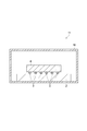
- FIG. 3 is a perspective view showing a heat dissipation sheet according to another embodiment.
- the first thermally conductive resin layer 8B has cuts 10 (a plurality of cut lines) on the surface (surface opposite to the conductive layer 7). .
- the thermal radiation sheet 5B has high flexibility and high followability in addition to high thermal conductivity.
- the notch 10 is formed in only one of the thermally conductive resin layers (the first thermally conductive resin layer 8), but in another embodiment, the thermal conductive resin layer A cut may be formed in both (the first thermally conductive resin layer 8 and the second thermally conductive resin layer 9).
- a groove (groove having a predetermined width) may be provided in the heat conductive resin layer.
- a heat conductive sheet may be provided between the electronic component and the housing. When sandwiched between them, air that cannot be discharged remains in the groove of the thermally conductive resin layer, which may increase the thermal resistance (decrease in thermal conductivity).
- the heat conductive resin layers 8 and 9 are provided with cuts so that the layers in the heat dissipation sheet 5B are stacked. The repulsive force (force in the compression direction) generated in the direction can be released in the direction perpendicular to the stacking direction, and air is difficult to enter.
- the heat dissipation sheet 5B has high followability to the shape to be applied, it is difficult to apply an excessive load to the electronic component 4 and the housing 6, and the risk of damage is reduced.
- the heat dissipation sheet 5B follows the unevenness and exhibits high adhesion.
- the heat-radiation sheet 5B is excellent in adhesiveness, since the heat generated in the electronic component 4 can be dissipated more efficiently, the heat-dissipation sheet 5B also exhibits better heat dissipation.
- the heat dissipation sheet 5B is particularly suitable for an application in which a load is applied between the electronic component 4 and the housing 6. Therefore, the heat dissipation sheet 5B is preferably a non-adhesive sheet (non-adhesive sheet including the non-adhesive thermally conductive resin layers 8 and 9) that does not have adhesiveness.
- the cut 10 is composed of one or more linear cuts (hereinafter referred to as “cut lines”).
- the cut line has such a width that a streak of cutting traces can be seen.
- the width of the score line (the length in the short direction) makes it difficult for air to enter the heat-dissipating sheet 5B, further improving the thermal conductivity (further reducing the thermal resistance), and the flexibility of the heat-dissipating sheet 5B.
- the followability can be further improved, it is preferably as small as possible, preferably 300 ⁇ m or less, more preferably less than 300 ⁇ m, still more preferably 100 ⁇ m or less, and particularly preferably 50 ⁇ m or less.
- the width of the cut line (length in the short direction) may be 2 ⁇ m or more, preferably 2 ⁇ m or more and less than 300 ⁇ m, more preferably 2 ⁇ m or more and 50 ⁇ m or less.
- the cut line may be, for example, a straight line or a curved shape such as a meandering shape or a wavy shape.
- the wave shape may be, for example, a sine wave shape, a sawtooth wave shape, a rectangular wave shape, a trapezoidal wave shape, a triangular wave shape, or the like.
- the planar shape of the cut 10 is not particularly limited.
- the planar shape of the notch 10 is a lattice shape. That is, the cut 10 shown in FIG. 3 is configured by arranging a plurality of linear cut lines in a lattice shape in plan view.
- the quadrangular planar shape constituting the lattice may be, for example, a rectangular shape or a square shape.
- planar shape of the cut may be a linear shape, a broken line shape (perforated shape), a polygonal shape, an elliptical shape, a circular shape, or the like.
- the broken line shape (perforated line shape) is, for example, in which a plurality of straight cut lines are arranged in one direction (extending direction of cut lines) at a predetermined interval (parts with cut lines and parts without cut lines) Is a shape that is repeated alternately).
- the polygonal shape is not particularly limited, and examples thereof include a triangular shape, a quadrangular shape, a pentagonal shape, a hexagonal shape, and a star shape.
- examples of the quadrangular shape include a trapezoidal shape, a rhombus shape, and a parallelogram shape.
- the planar shape of the cuts 10 is preferably linear, wavy, diamond-shaped, circular, star-shaped, and lattice-shaped, more preferably linear-shaped, diamond-shaped, and lattice-shaped, and more preferably cut-in processing. From the viewpoint of workability at the time and high followability, it is in a lattice shape (particularly, a lattice shape in which the planar shape of each square constituting the lattice is a square shape).
- the vertical cross-sectional shape of the notch 10 (the shape seen from the direction perpendicular to the stacking direction of the layers constituting the heat-dissipating sheet 5B) is not particularly limited, but for example, V-shaped, Y-shaped, l-shaped (English lowercase letters) L) shape (straight line shape), diagonal shape (slash shape), etc., and from the viewpoint that it is easy to form the cut 10 even in a state where the layers constituting the heat dissipation sheet 5B are laminated, (Lowercase letter L) (straight line).
- the cut 10 is preferably unpenetrated (not penetrating in the thickness direction (lamination direction) in the heat conductive resin layers 8 and 9).
- the length of the non-penetrating portion (the length in the thickness direction (lamination direction) of the portion where the cut is not formed in the heat conductive resin layers 8 and 9) is 0.1 mm or more, 0.15 mm or more, and 0.0.
- the ratio of the depth of the cut 10 to the thickness of the heat conductive resin layers 8 and 9 is preferably 2%. Or more, 10% or more, 20% or more, 30% or more, or 40% or more, preferably 90% or less, 80% or less, or 70% or less, preferably 2% to 90%, more preferably It may be 30% to 80%, more preferably 40% to 70%.
- the ratio is in the above range, high flexibility and high followability can be easily obtained (for example, the compressive stress (when the compression rate is 20%) can be reduced by 5% or more compared to the case where no cut is provided).
- the thermal resistance can be further reduced (thermal conductivity can be further improved).
- the notch 10 can be formed by, for example, using a cutting means and moving the cutting means in any of the thickness direction (stacking direction) and the direction perpendicular thereto, or a combination thereof.
- the cutting means can be moved in any direction (shape) such as “oblique direction” or “wavy”.
- the cutting means may be, for example, a cutting blade, laser, water jet (water cutter) or the like, and is preferably a cutting blade because the cutting line is easy to narrow and easy to process.
- the method of forming the cut 10 may be slit processing using a cutting blade, processing using a laser knife, or the like.
- the difference in Asker C hardness before and after the cut is preferably 2 or more, more preferably 5 or more.
- This “difference in Asker C before and after cutting” can be calculated by “(Asker C hardness before cutting) ⁇ (Asker C hardness after cutting)”.
- the heat conductive resin layer in which the cut is formed is brought into contact with the electronic component 4.
- the cut 10 is formed in one of the first thermal conductive resin layer 8 that contacts the electronic component 4 and the second thermal conductive resin layer 9 that contacts the housing 6, FIG. It is preferable to form the notch 10 in the 1st heat conductive resin layer 8 which contacts the electronic component 4 like the electromagnetic wave shielding heat dissipation sheet 5B shown in FIG.
- the heat radiating sheet 5B can follow the shape of the contact surface of the electronic component 4 with the first thermally conductive resin layer 8 due to high followability, and stress is applied to the heat radiating sheet 5B due to high flexibility.
- the stress can be relieved, it is difficult to damage the electronic component 4.
- the heat dissipation sheet 5B has high thermal conductivity while having high flexibility and high followability, heat generated from the electronic component 4 can be transmitted to the housing 6 particularly efficiently. Therefore, in the electronic device 1, the heat from the electronic component 4 can be efficiently released to the outside of the electronic device 1.
- the electromagnetic wave shielding heat radiation sheet 5 has an electromagnetic wave shielding property, it is possible to confine electromagnetic waves generated from the electronic component 4 and to block external electromagnetic waves.
- the electromagnetic shielding heat dissipation sheet 5 also has insulation, the spatial distance between the electronic component 4 and the housing 6 may be narrow, and the electronic device 1 can be downsized.
- the housing 6 is a metal housing, the electromagnetic wave shielding property can be further improved.
- the electromagnetic wave shielding heat radiating sheet 5 can shield the electromagnetic waves, it is necessary to use a metal housing. Instead, it is possible to contribute to further miniaturization by securing heat dissipation using a radiation fin or the like.
- FIG. 4 is a schematic cross-sectional view showing a conventional electronic device.
- the conventional electronic device 11 is not provided with an electromagnetic wave shielding heat dissipating sheet, and the housing 16 blocks electromagnetic waves generated from the electronic component 4 and heat generated from the electronic component 4.
- the casing 16 is made of metal from the viewpoint of obtaining electromagnetic wave shielding properties and heat dissipation.
- the electronic component 4 and the casing 16 are secured. And a spatial distance is required. Therefore, it is difficult to reduce the size of the conventional electronic device 11.
- the electronic device 1 including the electromagnetic wave shielding heat dissipation sheet 5 of the present embodiment can suppress malfunction and noise due to electromagnetic waves. Moreover, it can provide as the electronic component 4 which can reduce the lifetime reduction of the electronic component 4 by a temperature rise, a distortion
- the electromagnetic wave shielding heat radiation sheet 5B has both electromagnetic wave shielding properties and thermal conductivity, has a reduced compressive load (stress), and has high followability to an application target such as the electronic component 4 or the like. Can be provided. Further, in the heat dissipating sheet 5B, since the notch 10 is provided instead of the so-called groove, air does not remain, the followability to the application target of the electronic component 4 and the like is high, and the adhesiveness is also high. Is also expensive.
- the heat dissipation sheet 5B is particularly suitable as an electromagnetic shielding material for electronic parts and a heat dissipation member.
- the heat radiation sheet 5B is preferably used as a heat radiating member for an electronic component that requires adhesion between the heat generating surface of the semiconductor element and the heat radiating surface such as a heat radiating fin.
- the heat radiating sheet 5B is suitably used for electromagnetic shielding materials and heat conducting members such as industrial members, and particularly suitable as a high heat conducting sheet and heat radiating member having high flexibility that can reduce compressive stress during mounting. It is used.
- thermoly conductive resin composition was prepared by mixing the conductive filler at a blending ratio (volume%) shown in Tables 1 to 3. The total amount of component (A) and component (B) was 100% by volume.
- the mass average molecular weight of the polyorganosiloxane was a value in terms of polystyrene determined from the results of gel permeation chromatography analysis. Separation was performed using a non-aqueous porous gel (polystyrene-dimethylbenzene copolymer), toluene was used as the mobile phase, and a differential refractometer (RI) was used for detection.
- RI differential refractometer
- thermally conductive filler The following aluminum oxide (alumina) was used as the thermally conductive filler.
- total filler volume%) of the thermally conductive filler is the total amount of each spherical filler and each crystalline alumina used.
- the average particle diameter of the thermally conductive filler was measured using “Laser Diffraction Particle Size Analyzer SALD-20” manufactured by Shimadzu Corporation.
- SALD-20 “Laser Diffraction Particle Size Analyzer SALD-20” manufactured by Shimadzu Corporation.
- 5 g of 50 cc pure water and a thermally conductive filler powder to be measured were added to a glass beaker, stirred using a spatula, and then subjected to dispersion treatment for 10 minutes with an ultrasonic cleaner.
- the solution of the thermally conductive filler powder that had been subjected to the dispersion treatment was added drop by drop to the sampler portion of the apparatus using a dropper, and measurement was performed when the absorbance was stable.
- the particle size distribution is calculated from the data of the light intensity distribution of the diffracted / scattered light by the particles detected by the sensor.
- the average particle size is obtained by multiplying the value of the measured particle size by the relative particle amount (difference%) and dividing by the total relative particle amount (100%).
- an average particle diameter is an average diameter of particle
- D50 becomes a particle size with the largest appearance rate.
- the obtained heat conductive resin composition was formed on one surface of each conductive layer shown in Tables 1 and 2 with a thickness shown in Tables 1 and 2. After placing so as to obtain a conductive resin layer, heat curing was performed at 110 ° C. for 8 hours. Then, after arrange
- notches were formed in one or both of the heat conductive resin layers in the heat dissipation sheet obtained in Example 8. More specifically, using a cutting blade, linear cutting lines were made in two directions perpendicular to one or both of the thermally conductive resin layers to form a grid-shaped cutting.
- the width of the score line (the length in the short direction) is 50 ⁇ m or less
- the plane shape of each quadrangle constituting the lattice is 1.5 mm ⁇ 1.5 mm square
- the number of quadrilaterals constituting the lattice is 15 mm.
- the ratio of the depth to the depth of cut (length in the thickness direction) and the thickness of the heat conductive resin layer is as shown in Table 3.
- the electromagnetic shielding effect at 1 MHz was measured by the KEC method. If the shielding effect is 10 dB or more, it can be said that the electromagnetic wave shielding property is excellent, and if it is 20 dB or more, it can be said that the shielding effect is particularly excellent.
- Asker C hardness> Asker C hardness was measured by “Asker Rubber Hardness Tester C Type” manufactured by Kobunshi Keiki Co., Ltd. If the Asker C hardness is less than 40, the heat radiating sheet has high flexibility, and if the Asker C hardness is 15 or less, it can be said that the heat radiating sheet has particularly high flexibility.
- the electromagnetic shielding heat dissipation sheet of the present invention has high electromagnetic shielding properties and thermal conductivity, and also reduces the compressive load (compressive stress) when the sheet is used, and has high followability to the application target.
- the electromagnetic wave shielding heat dissipation sheet of the present invention can be suitably applied to an electromagnetic wave shield and a heat dissipation member for electronic components.
- an electromagnetic wave shielding heat dissipation sheet suitable for electric parts related to automobiles such as car navigation systems, radios, and automatic driving related devices).
Abstract
An electronic apparatus according to an aspect of the present invention is provided with an electronic component, an electromagnetic wave-shielding heat dissipation sheet, and a case that accommodates the electronic component and the electromagnetic wave-shielding heat dissipation sheet, wherein the electromagnetic wave-shielding heat dissipation sheet is provided with a first heat conductive resin layer, a conductive layer, and a second heat conductive resin layer in this order, and is disposed such that the first heat conductive resin layer is in contact with the electromagnetic component and the second heat conductive resin layer is in contact with the case.
Description
本発明は、電子機器及び電磁波シールド性放熱シートに関する。
The present invention relates to an electronic device and an electromagnetic wave shielding heat dissipation sheet.
電子部品の小型化、軽量化に伴い、電子部品の高密度実装化が進んでおり、誤作動の防止や人体への影響抑制のため、電子部品から生じる電磁波を遮蔽すること(電磁波シールド)の必要性が高まっている。従来、電磁波シールドの方法として、電子部品を金属製の筐体に密閉する方法が採られてきたが、この方法では、絶縁性を確保するために電子部品と筐体との空間距離が必要であり、電子機器の小型化の障害となっていた。これに対して、金属筐体に代わる電磁波シールド材として、シート状の電磁波シールド材が提案されている(例えば特許文献1)。
With the miniaturization and weight reduction of electronic components, electronic components are being mounted with high density. To prevent malfunctions and suppress the influence on the human body, shielding electromagnetic waves generated from electronic components (electromagnetic wave shield) There is a growing need. Conventionally, as a method of electromagnetic wave shielding, a method of sealing an electronic component in a metal casing has been adopted, but this method requires a spatial distance between the electronic component and the casing in order to ensure insulation. It was an obstacle to miniaturization of electronic devices. On the other hand, a sheet-like electromagnetic shielding material has been proposed as an electromagnetic shielding material instead of a metal casing (for example, Patent Document 1).
一方で、上述したような電子機器においては、電子部品から発生する熱による電子機器の故障などを防ぐために、電子機器の外部に放熱することも重要となる。しかし、特許文献1に記載されているようなシート状の電磁波シールド材は放熱性を有しておらず、放熱のためには、電子機器内に放熱部材を別途設ける必要がある。この場合、部材の数が増えるため、電子機器の小型化が困難になる。
On the other hand, in the electronic device as described above, it is also important to dissipate heat to the outside of the electronic device in order to prevent the electronic device from being damaged by heat generated from the electronic component. However, the sheet-like electromagnetic shielding material described in Patent Document 1 does not have heat dissipation properties, and it is necessary to separately provide a heat dissipation member in the electronic device for heat dissipation. In this case, since the number of members increases, it is difficult to reduce the size of the electronic device.
そこで、本発明の目的は、電子機器に電磁波シールド性及び放熱性を付与しつつ、電子機器を小型化することにある。
Therefore, an object of the present invention is to reduce the size of an electronic device while imparting electromagnetic shielding properties and heat dissipation to the electronic device.
本発明者らは、鋭意検討した結果、導電層の両面に熱伝導性樹脂層を積層したシートを用い、一方の熱伝導性樹脂層が電子部品に、他方の熱伝導性樹脂層が筐体にそれぞれ接触するように配置することにより、電子機器に電磁波シールド性及び放熱性を付与しつつ、電子機器の小型化が可能になることを見出した。
As a result of intensive studies, the present inventors have used a sheet in which a heat conductive resin layer is laminated on both sides of a conductive layer. One heat conductive resin layer is an electronic component and the other heat conductive resin layer is a housing. It has been found that the electronic device can be reduced in size while providing electromagnetic shielding properties and heat dissipation properties to the electronic device by arranging them so as to be in contact with each other.
すなわち、本発明は、いくつかの側面において、以下を提供可能である。
[1] 電子部品と、電磁波シールド性放熱シートと、電子部品及び電磁波シールド性放熱シートを収容する筐体と、を備え、電磁波シールド性放熱シートは、第1の熱伝導性樹脂層と、導電層と、第2の熱伝導性樹脂層とをこの順に備え、かつ、第1の熱伝導性樹脂層が電子部品に接触し、第2の熱伝導性樹脂層が筐体に接触するように配置されている、電子機器。
[2] 導電層が、金属箔又は金属メッシュで形成されている、[1]に記載の電子機器。
[3] 導電層が、アルミニウム、銅、銀及び金からなる群より選ばれる少なくとも1種を含む、[1]又は[2]に記載の電子機器。
[4] 第1の熱伝導性樹脂層及び第2の熱伝導性樹脂層が、それぞれ、シリコーン樹脂及び熱伝導性フィラーを含む、[1]~[3]のいずれかに記載の電子機器。
[5] 熱伝導性フィラーの含有量が、第1の熱伝導性樹脂層及び第2の熱伝導性樹脂層のそれぞれに対して40~85体積%である、[4]に記載の電子機器。
[6] 第1の熱伝導性樹脂層及び第2の熱伝導性樹脂層の少なくとも一方に複数の切り込みが形成されている、[1]~[5]のいずれかに記載の電子機器。
[7] 第1の熱伝導性樹脂層と、導電層と、第2の熱伝導性樹脂層とをこの順に備える、電磁波シールド性放熱シート。
[8] 導電層が、金属箔又は金属メッシュで形成されている、[7]に記載の電磁波シールド性放熱シート。
[9] 導電層が、アルミニウム、銅、銀及び金からなる群より選ばれる少なくとも1種を含む、[7]又は[8]に記載の電磁波シールド性放熱シート。
[10] 第1の熱伝導性樹脂層及び第2の熱伝導性樹脂層が、それぞれ、シリコーン樹脂及び熱伝導性フィラーを含む、[7]~[9]のいずれかに記載の電磁波シールド性放熱シート。
[11] 熱伝導性フィラーの含有量が、第1の熱伝導性樹脂層及び第2の熱伝導性樹脂層のそれぞれに対して40~85体積%である、[10]に記載の電磁波シールド性放熱シート。
[12] 第1の熱伝導性樹脂層及び第2の熱伝導性樹脂層の少なくとも一方に複数の切り込みが形成されている、[7]~[11]のいずれかに記載の電磁波シールド性放熱シート。 That is, the present invention can provide the following in some aspects.
[1] An electronic component, an electromagnetic wave shielding heat radiation sheet, and a housing that houses the electronic component and the electromagnetic wave shielding heat radiation sheet, the electromagnetic wave shielding heat radiation sheet, the first thermally conductive resin layer, the conductive material And a second heat conductive resin layer in this order, the first heat conductive resin layer is in contact with the electronic component, and the second heat conductive resin layer is in contact with the housing. Electronic equipment that is arranged.
[2] The electronic device according to [1], wherein the conductive layer is formed of a metal foil or a metal mesh.
[3] The electronic device according to [1] or [2], wherein the conductive layer includes at least one selected from the group consisting of aluminum, copper, silver, and gold.
[4] The electronic device according to any one of [1] to [3], wherein each of the first heat conductive resin layer and the second heat conductive resin layer includes a silicone resin and a heat conductive filler.
[5] The electronic device according to [4], wherein the content of the heat conductive filler is 40 to 85% by volume with respect to each of the first heat conductive resin layer and the second heat conductive resin layer. .
[6] The electronic device according to any one of [1] to [5], wherein a plurality of cuts are formed in at least one of the first heat conductive resin layer and the second heat conductive resin layer.
[7] An electromagnetic wave shielding heat dissipating sheet comprising a first heat conductive resin layer, a conductive layer, and a second heat conductive resin layer in this order.
[8] The electromagnetic wave shielding heat dissipation sheet according to [7], wherein the conductive layer is formed of a metal foil or a metal mesh.
[9] The electromagnetic wave shielding heat dissipation sheet according to [7] or [8], wherein the conductive layer contains at least one selected from the group consisting of aluminum, copper, silver and gold.
[10] The electromagnetic wave shielding property according to any one of [7] to [9], wherein the first thermally conductive resin layer and the second thermally conductive resin layer each include a silicone resin and a thermally conductive filler. Heat dissipation sheet.
[11] The electromagnetic wave shield according to [10], wherein the content of the heat conductive filler is 40 to 85% by volume with respect to each of the first heat conductive resin layer and the second heat conductive resin layer. Heat dissipation sheet.
[12] The electromagnetic wave shielding heat dissipation according to any one of [7] to [11], wherein a plurality of cuts are formed in at least one of the first thermal conductive resin layer and the second thermal conductive resin layer. Sheet.
本発明によれば、電子機器に電磁波シールド性及び放熱性を付与しつつ、電子機器を小型化することが可能となる。
According to the present invention, it is possible to reduce the size of an electronic device while imparting electromagnetic shielding properties and heat dissipation to the electronic device.
以下、図面を適宜参照しながら、本発明の実施形態について詳細に説明する。
Hereinafter, embodiments of the present invention will be described in detail with appropriate reference to the drawings.
図1は、一実施形態に係る電子機器を示す模式断面図である。図1に示すように、一実施形態に係る電子機器1は、基板2と、複数の半田3を介して基板2上に設けられた電子部品4と、電磁波シールド性放熱シート(以下、単に「放熱シート」ともいう)5と、これらを収容する筐体6とを備えている。
FIG. 1 is a schematic cross-sectional view showing an electronic apparatus according to an embodiment. As shown in FIG. 1, an electronic device 1 according to an embodiment includes a substrate 2, an electronic component 4 provided on the substrate 2 via a plurality of solders 3, an electromagnetic wave shielding heat radiation sheet (hereinafter simply referred to as “ 5) and a housing 6 for housing them.
基板2は、例えば、プリント基板等であってよい。電子部品4は、例えば、LSI(大規模集積回路)、IC(集積回路)、半導体パッケージ等であってよい。半田3は、基板2における配線と電子部品4とを互いに電気的に接続している。半田3は、例えば、半田ボールであってよく、電子部品4のピンが基板2に挿入された状態で半田付けにより形成されたものであってもよい。
The substrate 2 may be, for example, a printed circuit board. The electronic component 4 may be, for example, an LSI (Large Scale Integrated Circuit), an IC (Integrated Circuit), a semiconductor package, or the like. The solder 3 electrically connects the wiring on the substrate 2 and the electronic component 4 to each other. The solder 3 may be, for example, a solder ball, and may be formed by soldering in a state where the pins of the electronic component 4 are inserted into the substrate 2.
筐体6は、例えば、中空の略直方体状の箱体である。筐体6は、金属製又は樹脂製であってよい。筐体6は、例えば、電磁波シールド性を有する金属製の筐体であってよく、電磁波シールド性を有しない樹脂製の筐体であってもよい。この電子機器1は電磁波シールド性を有する放熱シート5を備えているため、筐体6が電磁波シールド性を有さないもの(例えば樹脂製の筐体)であっても、電子部品4から発生する電磁波は、放熱シート5によって好適に遮蔽され、電子機器1の外部に漏れにくくなっている。
The housing 6 is, for example, a hollow, substantially rectangular parallelepiped box. The housing 6 may be made of metal or resin. The housing 6 may be, for example, a metal housing having electromagnetic shielding properties or a resin housing having no electromagnetic shielding properties. Since the electronic device 1 includes the heat radiation sheet 5 having electromagnetic wave shielding properties, the electronic device 1 is generated from the electronic component 4 even if the housing 6 does not have electromagnetic wave shielding properties (for example, a resin housing). The electromagnetic wave is suitably shielded by the heat dissipation sheet 5 and is difficult to leak out of the electronic device 1.
放熱シート5は、導電層(導電性基材)7と、導電層7の両面にそれぞれ積層された熱伝導性樹脂層8,9とを備えている。図2は、放熱シート5の一実施形態を示す斜視図である。図2に示すように、一実施形態に係る放熱シート5Aは、第1の熱伝導性樹脂層8Aと、導電層7と、第2の熱伝導性樹脂層9とをこの順に備えている。第1の熱伝導性樹脂層8A、導電層7及び第2の熱伝導性樹脂層9は、互いに略同一の平面形状(例えば矩形状)を有しており、各層の端面が互いに揃うように積層されて放熱シート5を構成している。
The heat dissipation sheet 5 includes a conductive layer (conductive substrate) 7 and thermally conductive resin layers 8 and 9 laminated on both surfaces of the conductive layer 7, respectively. FIG. 2 is a perspective view showing an embodiment of the heat dissipation sheet 5. As shown in FIG. 2, the heat dissipation sheet 5 </ b> A according to the embodiment includes a first heat conductive resin layer 8 </ b> A, a conductive layer 7, and a second heat conductive resin layer 9 in this order. The first heat conductive resin layer 8A, the conductive layer 7, and the second heat conductive resin layer 9 have substantially the same planar shape (for example, a rectangular shape) so that the end faces of the respective layers are aligned with each other. The heat dissipation sheet 5 is configured by being laminated.
電子機器1においては、放熱シート5は、第1の熱伝導性樹脂層8が電子部品4に接触し、第2の熱伝導性樹脂層9が筐体6に接触するように配置されている。これにより、電子部品4で発生した熱を、筐体6を介して外部に放出することができる。
In the electronic device 1, the heat dissipation sheet 5 is disposed such that the first heat conductive resin layer 8 is in contact with the electronic component 4 and the second heat conductive resin layer 9 is in contact with the housing 6. . Thereby, the heat generated in the electronic component 4 can be released to the outside through the housing 6.
導電層7は、金属箔又は金属メッシュで形成されていることが好ましい。導電層7は、金属箔又は金属メッシュを構成する金属として、例えば、アルミニウム、銅、銀及び金からなる群より選ばれる少なくとも1種を含んでいる。金属箔は、アルミニウム箔、銅箔、銀箔又は金箔であってよく、好適な比重が得られ、電磁波シールド性に更に優れる観点から、好ましくは、アルミニウム箔又は銅箔である。
The conductive layer 7 is preferably formed of a metal foil or a metal mesh. The conductive layer 7 includes, for example, at least one selected from the group consisting of aluminum, copper, silver, and gold as a metal constituting the metal foil or the metal mesh. The metal foil may be an aluminum foil, a copper foil, a silver foil, or a gold foil, and is preferably an aluminum foil or a copper foil from the viewpoint of obtaining a suitable specific gravity and further excellent electromagnetic wave shielding properties.
金属メッシュは、上述した金属の繊維がメッシュ状に編みこまれているものであってよく、天然繊維や合成繊維等の有機繊維、又は無機繊維に、導電性金属をメッキ、スパッタ、蒸着などによって被覆したものがメッシュ状になっているものでもよい。天然繊維としては、綿や麻などが挙げられる。合成繊維としては、ポリエステル繊維、ポリオレフィン繊維、アラミド繊維などが挙げられる。無機繊維としては、炭素繊維やガラス繊維が挙げられる。導電性金属は、上述したアルミニウム、銅、銀又は金であってよく、ニッケル又は亜鉛であってもよい。
The metal mesh may be one in which the above-described metal fibers are knitted into a mesh shape, and conductive fibers are plated, sputtered, or vapor deposited on organic fibers or inorganic fibers such as natural fibers or synthetic fibers. What was covered may be a mesh. Examples of natural fibers include cotton and hemp. Examples of synthetic fibers include polyester fibers, polyolefin fibers, and aramid fibers. Examples of the inorganic fiber include carbon fiber and glass fiber. The conductive metal may be aluminum, copper, silver or gold as described above, and may be nickel or zinc.
導電層7の厚さは、電磁波シールド性を更に向上させる観点から、好ましくは10μm以上であり、放熱シート5の柔軟性や重量が好適である観点から、好ましくは300μm以下であり、200μm以下、100μm以下、又は50μm以下であってもよい。
The thickness of the conductive layer 7 is preferably 10 μm or more from the viewpoint of further improving the electromagnetic wave shielding properties, and preferably 300 μm or less, 200 μm or less, from the viewpoint that the flexibility and weight of the heat dissipation sheet 5 are suitable. It may be 100 μm or less, or 50 μm or less.
熱伝導性樹脂層8,9は、特に限定されないが、例えば、(A)樹脂成分及び(B)熱伝導性フィラーを含む熱伝導性樹脂組成物の硬化物で形成されている。
Although the heat conductive resin layers 8 and 9 are not particularly limited, for example, they are formed of a cured product of a heat conductive resin composition containing (A) a resin component and (B) a heat conductive filler.
<(A)樹脂成分>
(A)樹脂成分は、柔軟性に優れ、熱伝導性(放熱性)に更に優れる放熱シート5を得ることができる観点から、好ましくはシリコーン樹脂を含む(a)シリコーン樹脂成分である。 <(A) Resin component>
(A) The resin component is preferably a (a) silicone resin component containing a silicone resin from the viewpoint of obtaining a heat-dissipatingsheet 5 having excellent flexibility and further excellent thermal conductivity (heat dissipation).
(A)樹脂成分は、柔軟性に優れ、熱伝導性(放熱性)に更に優れる放熱シート5を得ることができる観点から、好ましくはシリコーン樹脂を含む(a)シリコーン樹脂成分である。 <(A) Resin component>
(A) The resin component is preferably a (a) silicone resin component containing a silicone resin from the viewpoint of obtaining a heat-dissipating
(a)シリコーン樹脂成分は、特に限定されず、例えば、過酸化物架橋、縮合反応架橋、付加反応架橋、紫外線架橋等による硬化反応によって硬化し得る成分であってよく、好ましくは、付加反応架橋による硬化反応によって硬化し得る成分である。(a)シリコーン樹脂成分は、好ましくは付加反応型のシリコーン樹脂を含み、より好ましくは一液付加反応型又は二液付加反応型のシリコーン樹脂を含む。
(A) The silicone resin component is not particularly limited, and may be a component that can be cured by a curing reaction such as peroxide crosslinking, condensation reaction crosslinking, addition reaction crosslinking, ultraviolet crosslinking, etc., preferably addition reaction crosslinking. It is a component that can be cured by a curing reaction. The (a) silicone resin component preferably contains an addition reaction type silicone resin, and more preferably contains a one-component addition reaction type or two-component addition reaction type silicone resin.
(a)シリコーン樹脂成分は、好ましくは、(a1)少なくとも末端又は側鎖にビニル基を有するオルガノポリシロキサン(以下、「ビニル基を有するオルガノポリシロキサン」ともいう。)と、(a2)少なくとも末端又は側鎖に2個以上のH-Si基を有するオルガノポリシロキサン(以下、「H-Si基を有するオルガノポリシロキサン」ともいう。)と、を含む二液付加反応型液状シリコーン樹脂成分である。
(A) The silicone resin component is preferably (a1) an organopolysiloxane having a vinyl group at least at the terminal or side chain (hereinafter also referred to as “organopolysiloxane having a vinyl group”), and (a2) at least the terminal. Or an organopolysiloxane having two or more H—Si groups in the side chain (hereinafter also referred to as “organopolysiloxane having an H—Si group”), and a two-component addition reaction type liquid silicone resin component. .
(a)シリコーン樹脂成分において、(a1)と(a2)とが反応し硬化することにより、シリコーンゴムが形成される。このような(a)シリコーン樹脂成分を(B)熱伝導性フィラーと共に用いることにより、熱伝導性樹脂組成物中に例えば40~85体積%という大きい含有量で熱伝導性フィラーを含有させる場合であっても、高い柔軟性の熱伝導性樹脂層を得ることができる。更に、熱伝導性フィラーを多く含有させることができるので、高熱伝導性の熱伝導性樹脂層を得ることができる。
(A) In the silicone resin component, (a1) and (a2) react and cure to form silicone rubber. By using such a (a) silicone resin component together with (B) a thermally conductive filler, the thermally conductive resin composition contains the thermally conductive filler at a large content of, for example, 40 to 85% by volume. Even if it exists, a highly flexible heat conductive resin layer can be obtained. Furthermore, since a large amount of thermally conductive filler can be contained, a highly thermally conductive thermally conductive resin layer can be obtained.
(a1)は、少なくとも末端又は側鎖のどこかにビニル基を有するオルガノポリシロキサンであり、直鎖状構造又は分岐状構造のいずれを有していてもよい。ビニル基を有するオルガノポリシロキサンは、例えば、オルガノポリシロキサンの分子内の(Si-R)で表される構造において、R部分の一部がビニル基になっているものである。
(A1) is an organopolysiloxane having a vinyl group at least at the terminal or side chain, and may have either a linear structure or a branched structure. The organopolysiloxane having a vinyl group is, for example, a structure represented by (Si—R) in the organopolysiloxane molecule, wherein a part of the R portion is a vinyl group.
(a1)ビニル基を有するオルガノポリシロキサンは、具体的には、例えば、以下の式(a1-1)で表される構造単位又は式(a1-2)で表される末端構造を有していてよい。(a1)ビニル基を有するオルガノポリシロキサンは、例えば、式(a1-1)で表される構造単位及び式(a1-3)で表される構造単位を有していてよく、式(a1-2)で表される末端構造及び式(a1-3)で表される構造単位を有していてもよい。ただし、(a1)ビニル基を有するオルガノポリシロキサンは、これらの構造単位又は末端構造を有するものに限定されない。

(A1) The organopolysiloxane having a vinyl group specifically has, for example, a structural unit represented by the following formula (a1-1) or a terminal structure represented by the formula (a1-2): It's okay. (A1) The organopolysiloxane having a vinyl group may have, for example, a structural unit represented by the formula (a1-1) and a structural unit represented by the formula (a1-3). It may have a terminal structure represented by 2) and a structural unit represented by formula (a1-3). However, (a1) the organopolysiloxane having a vinyl group is not limited to those having these structural units or terminal structures.
(a1)中のビニル基の含有量は、0.01モル%以上であってよく、15モル%以下又は5モル%以下であってよく、好ましくは0.01~15モル%、より好ましくは0.01~5モル%である。本発明における「ビニル基の含有量」とは、(a1)中のビニル基及びSi原子の合計モル数に対するビニル基のモル数の割合(モル%)を意味する。
The content of the vinyl group in (a1) may be 0.01 mol% or more, 15 mol% or less or 5 mol% or less, preferably 0.01 to 15 mol%, more preferably 0.01 to 5 mol%. The “vinyl group content” in the present invention means the ratio (mol%) of the number of moles of vinyl groups to the total number of moles of vinyl groups and Si atoms in (a1).
ビニル基の含有量は、以下の方法により測定される。
NMRによりビニル基の含有量を測定する。具体的には、例えばJEOL社製 ECP-300NMRを使用し、重溶媒として重クロロホルムにビニル基を有するオルガノポリシロキサンを溶解して測定する。測定結果から算出されるビニル基のモル数及びSi原子(Si-CH3基、H-Si基等に由来する)のモル数の合計を100モル%とした場合のビニル基のモル数の割合を、ビニル基の含有量(モル%)とする。 The vinyl group content is measured by the following method.
The vinyl group content is measured by NMR. Specifically, for example, ECP-300 NMR manufactured by JEOL is used, and measurement is performed by dissolving an organopolysiloxane having a vinyl group in deuterated chloroform as a heavy solvent. Ratio of the number of moles of vinyl group when the total number of moles of vinyl group calculated from the measurement results and the number of moles of Si atoms (derived from Si—CH 3 group , H—Si group, etc.) is 100% Is the vinyl group content (mol%).
(a1)ビニル基を有するオルガノポリシロキサンは、好ましくは、ビニル基に加えてアルキル基を有するアルキルポリシロキサンである。このアルキル基は、好ましくは炭素数1~3のアルキル基(例えば、メチル基、エチル基等)であり、より好ましくはメチル基である。(a1)ビニル基を有するオルガノポリシロキサンは、末端及び/又は側鎖にビニル基を有するメチルポリシロキサンであってよい。
(A1) The organopolysiloxane having a vinyl group is preferably an alkylpolysiloxane having an alkyl group in addition to the vinyl group. This alkyl group is preferably an alkyl group having 1 to 3 carbon atoms (for example, a methyl group, an ethyl group, etc.), and more preferably a methyl group. (A1) The organopolysiloxane having a vinyl group may be a methylpolysiloxane having a vinyl group at the terminal and / or side chain.
(a1)ビニル基を有するオルガノポリシロキサンの質量平均分子量(重量平均分子量ともいう。以下同じ。)は、好ましくは400,000未満であり、200,000以下であってよく、10,000以上又は15,000以上であってよく、より好ましくは10,000~200,000であり、更に好ましくは15,000~200,000である。(a1)ビニル基を有するオルガノポリシロキサンの質量平均分子量は、実施例に記載の方法により測定される。
(A1) The mass average molecular weight (also referred to as weight average molecular weight, hereinafter the same) of the organopolysiloxane having a vinyl group is preferably less than 400,000 and may be 200,000 or less, or 10,000 or more or It may be 15,000 or more, more preferably 10,000 to 200,000, still more preferably 15,000 to 200,000. (A1) The mass average molecular weight of the organopolysiloxane having a vinyl group is measured by the method described in Examples.
(a2)は、少なくとも末端又は側鎖のどこかに2個以上のH-Si基を有するオルガノポリシロキサンであり、直鎖状構造又は分岐状構造のいずれを有していてもよい。H-Si基を有するオルガノポリシロキサンは、例えば、オルガノポリシロキサンの分子内の(Si-R)で表される構造において、R部分の一部がH(水素原子)になっていているものである。
(A2) is an organopolysiloxane having two or more H—Si groups at least at either the terminal or the side chain, and may have either a linear structure or a branched structure. An organopolysiloxane having an H—Si group is, for example, a structure represented by (Si—R) in the molecule of the organopolysiloxane, wherein a part of the R portion is H (hydrogen atom). is there.
(a2)H-Si基を有するオルガノポリシロキサンは、具体的には、例えば、以下の式(a2-1)で表される構造単位又は式(a2-2)で表される末端構造を有していてよい。(a2)H-Si基を有するオルガノポリシロキサンは、例えば、式(a2-1)で表される構造単位及び式(a2-3)で表される構造単位を有していてよく、式(a2-2)で表される末端構造及び式(a2-3)で表される構造単位を有していてもよい。ただし、(a2)H-Si基を有するオルガノポリシロキサンは、これらの構造単位又は末端構造を有するものに限定されない。

(A2) Specifically, the organopolysiloxane having an H—Si group has, for example, a structural unit represented by the following formula (a2-1) or a terminal structure represented by the formula (a2-2): You can do it. (A2) The organopolysiloxane having an H—Si group may have, for example, a structural unit represented by the formula (a2-1) and a structural unit represented by the formula (a2-3). It may have a terminal structure represented by a2-2) and a structural unit represented by formula (a2-3). However, the (a2) organopolysiloxane having an H—Si group is not limited to those having these structural units or terminal structures.
(a2)中のH-Si基の含有量は、0.01モル%以上であってよく、15モル%以下又は5モル%以下であってよく、好ましくは0.01~15モル%、より好ましくは0.01~5モル%である。本発明における「H-Si基の含有量」とは、(a2)中のSi原子のモル数に対するH-Si基のモル数の割合(モル%)を意味する。
The content of H—Si groups in (a2) may be 0.01 mol% or more, 15 mol% or less or 5 mol% or less, preferably 0.01 to 15 mol%, more Preferably, it is 0.01 to 5 mol%. The “content of H—Si groups” in the present invention means the ratio (mol%) of the number of moles of H—Si groups to the number of moles of Si atoms in (a2).
H-Si基の含有量は、以下の方法により測定される。
NMRによりH-Si基含有量を測定する。具体的には、例えばJEOL社製 ECP-300NMRを使用し、重溶媒として重クロロホルムにH-Si基を有するオルガノポリシロキサンを溶解して測定する。測定結果から算出されるSi原子(Si-CH3基、H-Si基等に由来する)のモル数を100モル%とした場合のH-Si基のモル数の割合を、H-Si基の含有量(モル%)とする。 The content of H—Si groups is measured by the following method.
The H—Si group content is measured by NMR. Specifically, for example, ECP-300 NMR manufactured by JEOL is used, and measurement is performed by dissolving an organopolysiloxane having an H—Si group in deuterated chloroform as a heavy solvent. The ratio of the number of moles of H—Si groups when the number of moles of Si atoms (derived from Si—CH 3 groups , H—Si groups, etc.) calculated from the measurement results is 100 mol% Content (mol%).
(a2)H-Si基を有するオルガノポリシロキサンは、好ましくは、H-Si基に加えてアルキル基を有するアルキルポリシロキサンである。このアルキル基は、好ましくは炭素数1~3のアルキル基(例えば、メチル基、エチル基等)であり、より好ましくはメチル基である。(a2)H-Si基を有するオルガノポリシロキサンは、末端及び/又は側鎖にH-Si基を2個以上有するメチルポリシロキサンであってよい。
(A2) The organopolysiloxane having an H—Si group is preferably an alkylpolysiloxane having an alkyl group in addition to the H—Si group. This alkyl group is preferably an alkyl group having 1 to 3 carbon atoms (for example, a methyl group, an ethyl group, etc.), and more preferably a methyl group. (A2) The organopolysiloxane having an H—Si group may be a methyl polysiloxane having two or more H—Si groups at the terminal and / or side chain.
(a2)H-Si基を有するオルガノポリシロキサンの質量平均分子量は、好ましくは400,000以下であり、200,000以下であってよく、10,000以上又は15,000以上であってよく、より好ましくは10,000~200,000であり、更に好ましくは15,000~200,000である。(a2)H-Si基を有するオルガノポリシロキサンの質量平均分子量は、実施例に記載の方法により測定される。
(A2) The weight average molecular weight of the organopolysiloxane having an H—Si group is preferably 400,000 or less, 200,000 or less, 10,000 or more, or 15,000 or more, More preferably, it is 10,000 to 200,000, and still more preferably 15,000 to 200,000. (A2) The mass average molecular weight of the organopolysiloxane having an H—Si group is measured by the method described in Examples.
(a1)ビニル基を有するオルガノポリシロキサン及び(a2)H-Si基を有するオルガノポリシロキサンは、ポリシロキサン骨格の側鎖にフェニル基、トリフルオロプロピル基等のその他の有機基を有するその他の構造を更に含んでいてもよい。その他の構造を有する構造単位は、フェニルメチルシロキサン、ジフェニルシロキサンに由来する構造単位であってよい。(a)シリコーン樹脂を構成するオルガノポリシロキサンは、エポキシ基等の官能基を有する変性オルガノポリシロキサンであってもよい。
(A1) An organopolysiloxane having a vinyl group and (a2) an organopolysiloxane having an H—Si group have other structures having other organic groups such as a phenyl group and a trifluoropropyl group in the side chain of the polysiloxane skeleton. May further be included. The structural unit having other structure may be a structural unit derived from phenylmethylsiloxane or diphenylsiloxane. (A) The organopolysiloxane constituting the silicone resin may be a modified organopolysiloxane having a functional group such as an epoxy group.
(a)シリコーン樹脂成分の25℃での粘度は、100mPa・s以上又は350mPa・s以上であってよく、2,500mPa・s以下又は2,000mPa・s以下であってよく、例えば100~2,500mPa・sであり、好ましくは100~2,000mPa・sであり、より好ましくは350~2,000mPa・sである。(a)シリコーン樹脂成分の25℃での粘度が100mPa・s以上であると、熱伝導性樹脂層が裂けることを抑制できる点で有利であり、(a)シリコーン樹脂成分の25℃での粘度が2,500mPa・s以下であると、熱伝導性フィラーを高充填しやすくなる点で有利である。
(A) The viscosity of the silicone resin component at 25 ° C. may be 100 mPa · s or more or 350 mPa · s or more, may be 2,500 mPa · s or less, or 2,000 mPa · s or less, for example, 100 to 2 , 500 mPa · s, preferably 100 to 2,000 mPa · s, more preferably 350 to 2,000 mPa · s. (A) When the viscosity at 25 ° C. of the silicone resin component is 100 mPa · s or more, it is advantageous in that the thermal conductive resin layer can be prevented from tearing. (A) Viscosity at 25 ° C. of the silicone resin component Is 2,500 mPa · s or less, it is advantageous in that it is easy to highly fill the thermally conductive filler.
(a)シリコーン樹脂成分の25℃での粘度は、例えばBROOKFIELD社製B型粘度計「RVDVIT」を用いて測定できる。スピンドルにはfシャフトを使用し、20rpmでの粘度として測定される。
(A) The viscosity of the silicone resin component at 25 ° C. can be measured using, for example, a B-type viscometer “RVDVIT” manufactured by BROOKFIELD. The f-shaft is used as the spindle and is measured as the viscosity at 20 rpm.
(a)シリコーン樹脂成分は、好ましくは、熱硬化性のオルガノポリシロキサンを含む。(a)シリコーン樹脂成分は、ポリオルガノポリシロキサン(ベースポリマー、主剤ともいう)に加えて、硬化剤(架橋性オルガノポリシロキサン)を更に含んでいてもよい。(a)シリコーン樹脂成分は、付加反応を促進させるための付加反応触媒を更に含んでいてもよい。
(A) The silicone resin component preferably contains a thermosetting organopolysiloxane. (A) The silicone resin component may further contain a curing agent (crosslinkable organopolysiloxane) in addition to the polyorganopolysiloxane (also referred to as base polymer or main ingredient). (A) The silicone resin component may further contain an addition reaction catalyst for promoting the addition reaction.
上述したような(a)シリコーン樹脂成分として、市販品を使用することができる。市販品のシリコーン樹脂成分は、二液付加反応型液状シリコーンゴムとして、例えば、モメンティブ社製「TSE-3062」「X14-B8530」、東レダウコーニング社製「SE-1885A/B」等であってよいが、これらの具体的な市販品の範囲に限定されるものではない。
Commercially available products can be used as the (a) silicone resin component as described above. Examples of commercially available silicone resin components include two-component addition reaction type liquid silicone rubbers such as “TSE-3062” and “X14-B8530” manufactured by Momentive, “SE-1885A / B” manufactured by Toray Dow Corning, and the like. Although it is good, it is not limited to the range of these specific commercial products.
(A)樹脂成分は、上記(a)シリコーン樹脂成分に加えて、アクリル樹脂及びエポキシ樹脂等のその他の樹脂を更に含有していてもよい。
(A) The resin component may further contain other resins such as an acrylic resin and an epoxy resin in addition to the above (a) silicone resin component.
(A)樹脂成分((a)シリコーン樹脂成分)の含有量は、熱伝導性樹脂層の全体積に対して、10体積%以上又は15体積%以上であってよく、65体積%以下又は60体積%以下であってよく、好適には10~65体積%であり、より好適には15~60体積%である。(A)樹脂成分((a)シリコーン樹脂成分)の含有量が10体積%以上であると柔軟性を高くすることができ、65体積%以下であると熱伝導率の低下を回避しやすい点で有利である。
The content of the resin component (A) ((a) silicone resin component) may be 10% by volume or more or 15% by volume or more, and 65% by volume or less or 60% with respect to the total volume of the heat conductive resin layer. The volume may be not more than volume%, preferably 10 to 65 volume%, more preferably 15 to 60 volume%. (A) When the content of the resin component ((a) silicone resin component) is 10% by volume or more, flexibility can be increased, and when it is 65% by volume or less, it is easy to avoid a decrease in thermal conductivity. Is advantageous.
<(B)熱伝導性フィラー>
熱伝導性フィラーは、例えば熱伝導率が10W/m・K以上のフィラーである。熱伝導性フィラーは、酸化アルミニウム、酸化マグネシウム、窒化ホウ素、窒化アルミニウム、窒化珪素、炭化珪素、金属アルミニウム、黒鉛等であってよい。熱伝導性フィラーとして、これらを1種単独で又は2種以上組み合わせて使用することができる。熱伝導性フィラーは、好ましくは球状(好適には球形度が0.85以上)である。 <(B) Thermally conductive filler>
The thermally conductive filler is, for example, a filler having a thermal conductivity of 10 W / m · K or more. The thermally conductive filler may be aluminum oxide, magnesium oxide, boron nitride, aluminum nitride, silicon nitride, silicon carbide, metallic aluminum, graphite or the like. These can be used individually by 1 type or in combination of 2 or more types as a heat conductive filler. The thermally conductive filler is preferably spherical (suitably sphericity is 0.85 or more).
熱伝導性フィラーは、より高い熱伝導性を示すとともに、樹脂への充填性が良好なため、好ましくは酸化アルミニウムである。酸化アルミニウム(以下、「アルミナ」ともいう。)は、水酸化アルミニウム粉末の火炎溶射法、バイヤー法、アンモニウムミョウバン熱分解法、有機アルミニウム加水分解法、アルミニウム水中放電法、凍結乾燥法等のいずれの方法で製造されたものであってもよい。酸化アルミニウムは、粒径分布の制御及び粒子形状制御の点から、好ましくは水酸化アルミニウム粉末の火炎溶射法で製造されたものである。
The heat conductive filler is preferably aluminum oxide because it exhibits higher heat conductivity and good filling into the resin. Aluminum oxide (hereinafter also referred to as “alumina”) may be any of flame spraying method of aluminum hydroxide powder, Bayer method, ammonium alum pyrolysis method, organoaluminum hydrolysis method, aluminum underwater discharge method, freeze drying method, etc. It may be manufactured by a method. The aluminum oxide is preferably produced by flame spraying of aluminum hydroxide powder from the viewpoints of particle size distribution control and particle shape control.
アルミナの結晶構造は、単結晶体及び多結晶体のいずれでもよい。アルミナの結晶相は、高熱伝導性の点から、好ましくはα相である。アルミナの比重は、アルミナ粒子の内部に存在する空孔と低結晶相の存在割合が多くなることを避け、熱伝導率を更に高められる(例えば2.5W/m・K以上)観点から、好ましくは3.7以上である。
The crystal structure of alumina may be either a single crystal or a polycrystal. The crystal phase of alumina is preferably an α phase from the viewpoint of high thermal conductivity. The specific gravity of alumina is preferable from the viewpoint of avoiding an increase in the proportion of voids and low crystal phases present in the alumina particles and further increasing the thermal conductivity (for example, 2.5 W / m · K or more). Is 3.7 or more.
アルミナは、好ましくは球状である。アルミナが球状である場合、アルミナの球形度は、流動性が低下して熱伝導性樹脂層内でフィラーが偏析してしまうこと、及びそれに伴って物性のばらつきが大きくなることを抑制する観点から、好ましくは0.85以上である。球形度が0.85以上であるアルミナは、市販品として入手可能であり、例えば、デンカ株式会社製の球状アルミナDAW45S(商品名)、球状アルミナDAW05(商品名)、球状アルミナASFP20(商品名)等であってよい。
Alumina is preferably spherical. When the alumina is spherical, the sphericity of the alumina is from the viewpoint of suppressing the fluidity from decreasing and the filler segregating in the thermally conductive resin layer and the accompanying increase in variation in physical properties. , Preferably 0.85 or more. Alumina having a sphericity of 0.85 or more is available as a commercial product. For example, spherical alumina DAW45S (trade name), spherical alumina DAW05 (trade name), spherical alumina ASFP20 (trade name) manufactured by Denka Corporation. Etc.
熱伝導性フィラーは、好ましくは、粒度分布において、粒径10μm以上100μm以下、1μm以上10μm未満、又は1μm未満の範囲で極大値(ピーク)を有する。熱伝導性フィラーの粒度分布は、熱伝導性フィラーの分級・混合操作によって調整することができる。
The heat conductive filler preferably has a maximum value (peak) in the particle size distribution in the range of particle size of 10 μm to 100 μm, 1 μm to less than 10 μm, or less than 1 μm. The particle size distribution of the heat conductive filler can be adjusted by classification and mixing operation of the heat conductive filler.
熱伝導性フィラーは、好ましくは、粒径10μm以上100μm以下の範囲に極大値(ピーク)を有する熱伝導性フィラー(B-1)と、粒径1μm以上10μm未満の範囲に極大値(ピーク)を有する熱伝導性フィラー(B-2)と、粒径1μm未満の範囲に極大値(ピーク)を有する熱伝導性フィラー(B-3)と、を含む。熱伝導性フィラー(B-1)は、平均粒径10μm以上100μm以下の熱伝導性フィラーであってよい。熱伝導性フィラー(B-2)は、平均粒径1μm以上10μm未満の熱伝導性フィラーであってよい。熱伝導性フィラー(B-3)は、平均粒径1μm未満の熱伝導性フィラーであってよい。熱伝導性フィラーの粒度分布及び平均粒径は、実施例に記載に方法により測定される。
The thermally conductive filler is preferably a thermally conductive filler (B-1) having a maximum value (peak) in a particle size range of 10 μm to 100 μm and a maximum value (peak) in a particle size range of 1 μm to less than 10 μm. And a thermally conductive filler (B-3) having a maximum value (peak) in a particle size range of less than 1 μm. The thermally conductive filler (B-1) may be a thermally conductive filler having an average particle size of 10 μm or more and 100 μm or less. The heat conductive filler (B-2) may be a heat conductive filler having an average particle diameter of 1 μm or more and less than 10 μm. The thermally conductive filler (B-3) may be a thermally conductive filler having an average particle size of less than 1 μm. The particle size distribution and average particle size of the thermally conductive filler are measured by the method described in the examples.
熱伝導性フィラー(B-1)の割合は、熱伝導性フィラーの全体積に対して、好ましくは15体積%以上であり、20体積%以上、30体積%以上、又は40体積%以上であってよく、70体積%以下、60体積%以下、又は50体積%以下であってよく、より好ましくは20~60体積%である。
The ratio of the thermally conductive filler (B-1) is preferably 15% by volume or more, 20% by volume or more, 30% by volume or more, or 40% by volume or more with respect to the total volume of the thermally conductive filler. It may be 70% by volume or less, 60% by volume or less, or 50% by volume or less, and more preferably 20 to 60% by volume.
熱伝導性フィラー(B-2)の割合は、熱伝導性フィラーの全体積に対して、10体積%以上、12体積%以上、又は20体積%以上であってよく、40体積%以下、35体積%以下、又は30体積%以下であってよく、好ましくは10~30体積%、より好ましくは12~30体積%である。
The proportion of the heat conductive filler (B-2) may be 10% by volume or more, 12% by volume or more, or 20% by volume or more with respect to the total volume of the heat conductive filler, 40% by volume or less, 35 It may be not more than volume%, or not more than 30 volume%, preferably 10 to 30 volume%, more preferably 12 to 30 volume%.
熱伝導性フィラー(B-3)の割合は、熱伝導性フィラーの全体積に対して、5体積%以上又は8体積%以上であってよく、30体積%以下、25体積%以下、20体積%以下又は15体積%以下であってよく、好ましくは5~30体積%、より好ましくは8~20体積%である。
The proportion of the heat conductive filler (B-3) may be 5% by volume or more or 8% by volume or more with respect to the total volume of the heat conductive filler, and is 30% by volume or less, 25% by volume or less, 20% by volume. % Or less or 15% by volume or less, preferably 5 to 30% by volume, more preferably 8 to 20% by volume.
熱伝導性フィラーの含有量は、熱伝導性樹脂層の全体積に対して、20体積%以上又は30体積%以上であってよく、好ましくは35体積%以上又は40体積%以上であり、95体積%以下又は80体積%以下であってよく、好ましくは85体積%以下であり、より好ましくは40~85体積%である。熱伝導性フィラーの含有量が35体積%以上であると、熱伝導性樹脂層の熱伝導性が更に良好となる。熱伝導性フィラーの含有量が85体積%以下であると、熱伝導性樹脂組成物の流動性が悪くなるのを回避しやすく、熱伝導性樹脂層を作製しやすい。
The content of the heat conductive filler may be 20% by volume or more or 30% by volume or more, preferably 35% by volume or more, or 40% by volume or more with respect to the total volume of the heat conductive resin layer. It may be not more than volume% or not more than 80 volume%, preferably not more than 85 volume%, more preferably 40 to 85 volume%. When the content of the heat conductive filler is 35% by volume or more, the heat conductivity of the heat conductive resin layer is further improved. When the content of the heat conductive filler is 85% by volume or less, it is easy to avoid deterioration of the fluidity of the heat conductive resin composition, and it is easy to produce a heat conductive resin layer.
熱伝導性樹脂組成物は、アセチルアルコール類、マレイン酸エステル類などの反応遅延剤、粒径が十~数百μmのアエロジルやシリコーンパウダーなどの増粘剤、難燃剤、顔料などを更に含有することができる。
The thermally conductive resin composition further contains a reaction retarder such as acetyl alcohols and maleates, a thickener such as Aerosil or silicone powder having a particle size of 10 to several hundred μm, a flame retardant, and a pigment. be able to.
第1の熱伝導性樹脂層8及び第2の熱伝導性樹脂層9の厚さは、それぞれ、0.1mm以上であってよく、10mm以下であってよい。第1の熱伝導性樹脂層8及び第2の熱伝導性樹脂層9の熱伝導率は、それぞれ、好ましくは0.5W/mK以上である。
The thicknesses of the first heat conductive resin layer 8 and the second heat conductive resin layer 9 may be 0.1 mm or more and 10 mm or less, respectively. The thermal conductivities of the first thermal conductive resin layer 8 and the second thermal conductive resin layer 9 are each preferably 0.5 W / mK or more.
放熱シート5の厚さは、好ましくは0.2mm以上であり、1mm以上又は1.5mm以上であってよく、15mm以下又は12mm以下であってよく、好ましくは10mm以下であり、0.2mm~10mmであってもよい。放熱シート5の厚さが0.2mm以上であると、熱伝導性フィラーによる表面の粗さが大きくなること、及びそれに伴う熱伝導性の低下を抑制できる。放熱シート5の厚さが10mm以下であると、熱伝導性の低下を抑制できる。放熱シート5の厚さは、熱伝導性樹脂組成物の硬化後の厚さを基準とする。放熱シート5は、高い熱伝導性を有するものであり、0.5W/mK以上の熱伝導率を有する。
The thickness of the heat dissipating sheet 5 is preferably 0.2 mm or more, 1 mm or more or 1.5 mm or more, 15 mm or less or 12 mm or less, preferably 10 mm or less, preferably 0.2 mm to It may be 10 mm. When the thickness of the heat dissipating sheet 5 is 0.2 mm or more, it is possible to suppress an increase in surface roughness due to the heat conductive filler and a decrease in heat conductivity associated therewith. When the thickness of the heat dissipation sheet 5 is 10 mm or less, a decrease in thermal conductivity can be suppressed. The thickness of the heat radiation sheet 5 is based on the thickness after curing of the heat conductive resin composition. The heat dissipation sheet 5 has high thermal conductivity and has a thermal conductivity of 0.5 W / mK or more.
放熱シート5のアスカーC硬度は、好ましくは40未満であり、より好ましくは35以下であり、更に好ましくは30以下である。アスカーC硬度の下限値は、放熱シート5を取り扱う際のハンドリング性に優れる点から、好ましくは5以上である。
The Asker C hardness of the heat dissipation sheet 5 is preferably less than 40, more preferably 35 or less, and further preferably 30 or less. The lower limit value of Asker C hardness is preferably 5 or more from the viewpoint of excellent handling properties when handling the heat dissipation sheet 5.
放熱シート5は、例えば、導電層7の一方面上に、熱伝導性樹脂組成物を配置し、第1の熱伝導性樹脂層8及び第2の熱伝導性樹脂層9の一方を形成する工程(a-1)と、導電層7の他方面上に、熱伝導性樹脂組成物を配置し、第1の熱伝導性樹脂層8及び第2の熱伝導性樹脂層9の他方を形成する工程(a-2)と、を備える製造方法により製造される。
For example, the heat-dissipating sheet 5 is provided with a heat conductive resin composition on one surface of the conductive layer 7 to form one of the first heat conductive resin layer 8 and the second heat conductive resin layer 9. Step (a-1) and disposing the heat conductive resin composition on the other surface of the conductive layer 7 to form the other of the first heat conductive resin layer 8 and the second heat conductive resin layer 9 And a step (a-2).
放熱シート5の製造方法は、他の一実施形態において、樹脂フィルム(例えばPETフィルムなど)上に、熱伝導性樹脂組成物を配置し、第1の熱伝導性樹脂層8及び第2の熱伝導性樹脂層9の一方を形成する工程(b-1)と、工程(b-1)で形成された第1の熱伝導性樹脂層8又は第2の熱伝導性樹脂層9上に、導電層7を設ける(例えばラミネートする)工程(b-2)と、工程(b-2)で設けられた導電層7上に、熱伝導性樹脂組成物を配置し、第1の熱伝導性樹脂層8及び第2の熱伝導性樹脂層9の他方を形成する工程(b-3)と、を備えていてもよい。
In another embodiment, the manufacturing method of the heat dissipation sheet 5 is such that a thermally conductive resin composition is disposed on a resin film (for example, a PET film), and the first thermally conductive resin layer 8 and the second heat On the first thermal conductive resin layer 8 or the second thermal conductive resin layer 9 formed in the step (b-1) of forming one of the conductive resin layers 9 and the step (b-1), Step (b-2) for providing (for example, laminating) the conductive layer 7 and placing the heat conductive resin composition on the conductive layer 7 provided in the step (b-2) A step (b-3) of forming the other of the resin layer 8 and the second thermally conductive resin layer 9 may be provided.
各実施形態の製造方法において用いられる熱伝導性樹脂組成物は、公知の方法にて得ることができ、例えば、成分(A)及び(B)を混合することで得ることができる。混合には、ロールミル、ニーダー、バンバリーミキサー等の混合機が用いられる。
The heat conductive resin composition used in the production method of each embodiment can be obtained by a known method, for example, by mixing components (A) and (B). For mixing, a mixer such as a roll mill, a kneader, or a Banbury mixer is used.
工程(a-1)、工程(a-2)、工程(b-1)及び工程(b-3)において、熱伝導性樹脂組成物を配置する方法は、好ましくはドクターブレード法である。当該方法は、熱伝導性樹脂組成物の粘度に応じて、押し出し法、プレス法、カレンダーロール法等であってもよい。
In the step (a-1), the step (a-2), the step (b-1) and the step (b-3), the method of arranging the heat conductive resin composition is preferably a doctor blade method. The method may be an extrusion method, a press method, a calender roll method, or the like depending on the viscosity of the heat conductive resin composition.
工程(a-1)、工程(a-2)、工程(b-1)及び工程(b-3)においては、例えば、熱伝導性樹脂組成物を加熱硬化させることにより、第1の熱伝導性樹脂層8又は第2の熱伝導性樹脂層9を形成してよい。
In the step (a-1), the step (a-2), the step (b-1), and the step (b-3), for example, the heat conductive resin composition is heated and cured to thereby obtain the first heat conduction. The conductive resin layer 8 or the second thermally conductive resin layer 9 may be formed.
加熱硬化は、一般的な熱風乾燥機、遠赤外乾燥機、マイクロ波乾燥機等を用いて行われる。加熱温度は、好ましくは50~200℃である。加熱温度が50℃以上であると架橋が充分に進行しやすく、200℃以下であると加熱による劣化を抑制できる。加熱硬化時間は、好ましくは2~14時間である。
Heat curing is performed using a general hot air dryer, far-infrared dryer, microwave dryer, or the like. The heating temperature is preferably 50 to 200 ° C. When the heating temperature is 50 ° C. or higher, crosslinking is likely to proceed sufficiently, and when it is 200 ° C. or lower, deterioration due to heating can be suppressed. The heat curing time is preferably 2 to 14 hours.
放熱シート5の他の一実施形態においては、第1の熱伝導性樹脂層8及び第2の熱伝導性樹脂層9の表面(導電層7と反対側の表面)に切り込み(複数の切り込み線)が形成されていてよい。図3は、他の一実施形態に係る放熱シートを示す斜視図である。図3に示すように、この放熱シート5Bでは、第1の熱伝導性樹脂層8Bが、その表面(導電層7と反対側の表面)に切り込み10(複数の切り込み線)を有している。これにより、放熱シート5Bは、高熱伝導性に加えて、高柔軟性及び高追従性を有する。
In another embodiment of the heat-dissipating sheet 5, a cut (a plurality of cut lines) is made on the surfaces of the first heat conductive resin layer 8 and the second heat conductive resin layer 9 (surface opposite to the conductive layer 7). ) May be formed. FIG. 3 is a perspective view showing a heat dissipation sheet according to another embodiment. As shown in FIG. 3, in this heat radiation sheet 5B, the first thermally conductive resin layer 8B has cuts 10 (a plurality of cut lines) on the surface (surface opposite to the conductive layer 7). . Thereby, the thermal radiation sheet 5B has high flexibility and high followability in addition to high thermal conductivity.
図3に示す実施形態では、熱伝導性樹脂層の一方(第1の熱伝導性樹脂層8)のみに切り込み10が形成されているが、他の一実施形態では、熱伝導性樹脂層の両方(第1の熱伝導性樹脂層8及び第2の熱伝導性樹脂層9)に切り込みが形成されていてよい。
In the embodiment shown in FIG. 3, the notch 10 is formed in only one of the thermally conductive resin layers (the first thermally conductive resin layer 8), but in another embodiment, the thermal conductive resin layer A cut may be formed in both (the first thermally conductive resin layer 8 and the second thermally conductive resin layer 9).
ところで、従来の熱伝導性シートでは、熱伝導性樹脂層に溝(所定の幅を有する溝)が設けられている場合があるが、このような熱伝導性シートを電子部品と筐体との間に挟持した場合に、熱伝導性樹脂層の溝内に排出できない空気が残り、熱抵抗が上がる(熱伝導率が下がる)おそれがある。これに対し、放熱シート5Bが電子部品4と筐体6との間に挟持された場合、熱伝導性樹脂層8,9に切り込みが設けられていることによって、放熱シート5Bにおける各層の積層方向に生じる反発力(圧縮方向の力)を積層方向と垂直な方向に逃がすことができ、空気も入りにくくなる。
By the way, in the conventional heat conductive sheet, a groove (groove having a predetermined width) may be provided in the heat conductive resin layer. However, such a heat conductive sheet may be provided between the electronic component and the housing. When sandwiched between them, air that cannot be discharged remains in the groove of the thermally conductive resin layer, which may increase the thermal resistance (decrease in thermal conductivity). On the other hand, when the heat dissipation sheet 5B is sandwiched between the electronic component 4 and the housing 6, the heat conductive resin layers 8 and 9 are provided with cuts so that the layers in the heat dissipation sheet 5B are stacked. The repulsive force (force in the compression direction) generated in the direction can be released in the direction perpendicular to the stacking direction, and air is difficult to enter.
また、放熱シート5Bは、適用対象の形状に対する追従性が高いため、電子部品4及び筐体6に過度な荷重がかかりにくく、損傷が生じるリスクを低減できる。加えて、電子部品4及び筐体6に凹凸がある場合でも、放熱シート5Bが当該凹凸に追従して、高い密着性を発揮する。このように、放熱シート5Bは、密着性に優れることから、電子部品4で生じた熱をより効率良く放熱できるため、より優れた放熱性も発揮する。
Moreover, since the heat dissipation sheet 5B has high followability to the shape to be applied, it is difficult to apply an excessive load to the electronic component 4 and the housing 6, and the risk of damage is reduced. In addition, even when the electronic component 4 and the housing 6 are uneven, the heat dissipation sheet 5B follows the unevenness and exhibits high adhesion. Thus, since the heat-radiation sheet 5B is excellent in adhesiveness, since the heat generated in the electronic component 4 can be dissipated more efficiently, the heat-dissipation sheet 5B also exhibits better heat dissipation.
以上のことから、放熱シート5Bは、電子部品4と筐体6との間に荷重をかけて挟持されるような用途に特に好適である。したがって、放熱シート5Bは、好ましくは、粘着性を有さない非粘着性シート(非粘着性の熱伝導性樹脂層8,9を備える非粘着性シート)である。
From the above, the heat dissipation sheet 5B is particularly suitable for an application in which a load is applied between the electronic component 4 and the housing 6. Therefore, the heat dissipation sheet 5B is preferably a non-adhesive sheet (non-adhesive sheet including the non-adhesive thermally conductive resin layers 8 and 9) that does not have adhesiveness.
以上説明したような切り込み10の効果を好適に得る観点から、切り込み10は、1以上の線状の切り込み(以下「切り込み線」という)で構成されている。この切り込み線は、例えば、切断の痕跡のスジが見える程度の幅となっている。切り込み線の幅(短手方向の長さ)は、放熱シート5Bに空気が入りにくく、熱伝導率を更に向上させる(熱抵抗を更に低下させる)ことができると共に、放熱シート5Bの柔軟性及び追従性も更に向上させることができる観点から、小さいほど好ましく、好ましくは300μm以下、より好ましくは300μm未満、更に好ましくは100μm以下、特に好ましくは50μm以下である。切り込み線の幅(短手方向の長さ)は、2μm以上であってよく、好ましくは2μm以上300μm未満、より好ましくは2μm以上50μm以下であってよい。
From the viewpoint of suitably obtaining the effect of the cut 10 as described above, the cut 10 is composed of one or more linear cuts (hereinafter referred to as “cut lines”). For example, the cut line has such a width that a streak of cutting traces can be seen. The width of the score line (the length in the short direction) makes it difficult for air to enter the heat-dissipating sheet 5B, further improving the thermal conductivity (further reducing the thermal resistance), and the flexibility of the heat-dissipating sheet 5B. From the viewpoint that the followability can be further improved, it is preferably as small as possible, preferably 300 μm or less, more preferably less than 300 μm, still more preferably 100 μm or less, and particularly preferably 50 μm or less. The width of the cut line (length in the short direction) may be 2 μm or more, preferably 2 μm or more and less than 300 μm, more preferably 2 μm or more and 50 μm or less.
切り込み線は、例えば、直線状であってよく、蛇行状、波状等の曲線状であってよい。波状は、例えば、正弦波状、ノコギリ波状、矩形波状、台形波状、三角波状等であってよい。
The cut line may be, for example, a straight line or a curved shape such as a meandering shape or a wavy shape. The wave shape may be, for example, a sine wave shape, a sawtooth wave shape, a rectangular wave shape, a trapezoidal wave shape, a triangular wave shape, or the like.
切り込み10の平面形状は、特に限定されない。図3に示す実施形態では、切り込み10の平面形状は、格子状である。すなわち、図3に示す切り込み10は、複数の直線状の切り込み線が平面視において格子状に配置されることによって構成されている。格子を構成する各四角形の平面形状は、例えば、長方形状、正方形状等であってよい。
The planar shape of the cut 10 is not particularly limited. In the embodiment shown in FIG. 3, the planar shape of the notch 10 is a lattice shape. That is, the cut 10 shown in FIG. 3 is configured by arranging a plurality of linear cut lines in a lattice shape in plan view. The quadrangular planar shape constituting the lattice may be, for example, a rectangular shape or a square shape.
他の一実施形態では、切り込みの平面形状は、線状、破線状(ミシン目状)、多角形状、楕円形状、円形状等であってもよい。
In another embodiment, the planar shape of the cut may be a linear shape, a broken line shape (perforated shape), a polygonal shape, an elliptical shape, a circular shape, or the like.
破線状(ミシン目状)は、例えば、複数の直線状の切り込み線が所定の間隔で一方向(切り込み線の延在方向)に配列されている(切り込み線ありの部分と切り込み線なしの部分が交互に繰り返されている)形状をいう。
The broken line shape (perforated line shape) is, for example, in which a plurality of straight cut lines are arranged in one direction (extending direction of cut lines) at a predetermined interval (parts with cut lines and parts without cut lines) Is a shape that is repeated alternately).
多角形状としては、特に限定されないが、例えば、三角形状、四角形状、五角形状、六角形状、星形状等が挙げられる。四角形状としては、例えば、台形状、ひし形状、平行四辺形状等が挙げられる。
The polygonal shape is not particularly limited, and examples thereof include a triangular shape, a quadrangular shape, a pentagonal shape, a hexagonal shape, and a star shape. Examples of the quadrangular shape include a trapezoidal shape, a rhombus shape, and a parallelogram shape.
切り込み10の平面形状は、好ましくは、直線状、波状、ひし形状、円形状、星形状及び格子状であり、より好ましくは、直線状、ひし形状及び格子状であり、更に好ましくは、切り込み加工時の作業性及び高追従性の点から、格子状(特に、格子を構成する各四角形の平面形状が正方形状である格子状)である。
The planar shape of the cuts 10 is preferably linear, wavy, diamond-shaped, circular, star-shaped, and lattice-shaped, more preferably linear-shaped, diamond-shaped, and lattice-shaped, and more preferably cut-in processing. From the viewpoint of workability at the time and high followability, it is in a lattice shape (particularly, a lattice shape in which the planar shape of each square constituting the lattice is a square shape).
切り込み10の垂直断面形状(放熱シート5Bを構成する各層の積層方向に対して垂直な方向から見た形状)は、特に限定されないが、例えば、V字状、Y字状、l字(英小文字エル)状(一直線状)、斜め(スラッシュ)状等であってよく、放熱シート5Bを構成する各層が積層された状態でも切り込み10を形成することが容易である観点から、好ましくは、l字(英小文字エル)状(一直線状)である。
The vertical cross-sectional shape of the notch 10 (the shape seen from the direction perpendicular to the stacking direction of the layers constituting the heat-dissipating sheet 5B) is not particularly limited, but for example, V-shaped, Y-shaped, l-shaped (English lowercase letters) L) shape (straight line shape), diagonal shape (slash shape), etc., and from the viewpoint that it is easy to form the cut 10 even in a state where the layers constituting the heat dissipation sheet 5B are laminated, (Lowercase letter L) (straight line).
切り込み10は、好ましくは、未貫通である(熱伝導性樹脂層8,9において厚さ方向(積層方向)に貫通していない)。未貫通部分の長さ(熱伝導性樹脂層8,9において、切り込みが形成されていない部分の厚さ方向(積層方向)の長さ)は、0.1mm以上、0.15mm以上、0.2mm以上、又は0.25mm以上であってよく、6.0mm以下、5.0mm以下、4.0mm以下、又は3.0mm以下であってよく、好ましくは0.1mm~6.0mm、より好ましくは0.15mm~5.0mm、更に好ましくは0.2mm~4.0mm、特に好ましくは0.25mm~3.0mmである。
The cut 10 is preferably unpenetrated (not penetrating in the thickness direction (lamination direction) in the heat conductive resin layers 8 and 9). The length of the non-penetrating portion (the length in the thickness direction (lamination direction) of the portion where the cut is not formed in the heat conductive resin layers 8 and 9) is 0.1 mm or more, 0.15 mm or more, and 0.0. 2 mm or more, or 0.25 mm or more, 6.0 mm or less, 5.0 mm or less, 4.0 mm or less, or 3.0 mm or less, preferably 0.1 mm to 6.0 mm, more preferably Is 0.15 mm to 5.0 mm, more preferably 0.2 mm to 4.0 mm, and particularly preferably 0.25 mm to 3.0 mm.
熱伝導性樹脂層8,9の厚さに対する切り込み10の深さ(熱伝導性樹脂層8,9の厚さ方向(積層方向)における切り込み10の長さ)の割合は、好ましくは、2%以上、10%以上、20%以上、30%以上、又は40%以上であり、好ましくは、90%以下、80%以下、又は70%以下であり、好ましくは2%~90%、より好ましくは30%~80%、更に好ましくは40%~70%であってもよい。当該割合が上記の範囲であることによって、高柔軟性及び高追従性が得やすい(例えば、圧縮応力(圧縮率20%時)が、切り込みを設けない場合に比べて5%以上低減できる)とともに、熱抵抗も更に低減できる(熱伝導性を更に向上できる)。
The ratio of the depth of the cut 10 to the thickness of the heat conductive resin layers 8 and 9 (the length of the cut 10 in the thickness direction (stacking direction) of the heat conductive resin layers 8 and 9) is preferably 2%. Or more, 10% or more, 20% or more, 30% or more, or 40% or more, preferably 90% or less, 80% or less, or 70% or less, preferably 2% to 90%, more preferably It may be 30% to 80%, more preferably 40% to 70%. When the ratio is in the above range, high flexibility and high followability can be easily obtained (for example, the compressive stress (when the compression rate is 20%) can be reduced by 5% or more compared to the case where no cut is provided). The thermal resistance can be further reduced (thermal conductivity can be further improved).
切り込み10は、例えば切断手段を用いて、厚さ方向(積層方向)及びそれに垂直な方向のいずれか又はこれらを組み合わせて、当該切断手段を動かすことにより、形成することができる。なお、切断手段は、「斜め方向」や「波状」等の任意の方向(形状)にも動かすことができる。
The notch 10 can be formed by, for example, using a cutting means and moving the cutting means in any of the thickness direction (stacking direction) and the direction perpendicular thereto, or a combination thereof. The cutting means can be moved in any direction (shape) such as “oblique direction” or “wavy”.
切断手段は、例えば、切り込み刃、レーザー、ウォータージェット(ウォーターカッター)等であってよく、切り込み線を狭くしやすく加工が容易なため、好ましくは切りこみ刃である。切り込み10を形成する方法は、切り込み刃によるスリット加工、レーザーメスによる加工などであってよい。
The cutting means may be, for example, a cutting blade, laser, water jet (water cutter) or the like, and is preferably a cutting blade because the cutting line is easy to narrow and easy to process. The method of forming the cut 10 may be slit processing using a cutting blade, processing using a laser knife, or the like.
放熱シート5に切り込みを入れる場合は、切り込み前後のアスカーC硬度の差が、好ましくは2以上、より好ましくは5以上になるように切り込みを入れることが好適である。切り込み前後のアスカーC硬度の差が2以上であると、柔軟性の向上効果が得られやすく、追従性がより良好になる。この「切り込み前後のアスカーCの差」は、「(切り込み前のアスカーC硬度)-(切り込み後のアスカーC硬度)」にて算出することができる。
When making a cut in the heat dissipation sheet 5, it is preferable to make a cut so that the difference in Asker C hardness before and after the cut is preferably 2 or more, more preferably 5 or more. When the difference in Asker C hardness before and after cutting is 2 or more, an effect of improving flexibility is easily obtained, and the followability becomes better. This “difference in Asker C before and after cutting” can be calculated by “(Asker C hardness before cutting) − (Asker C hardness after cutting)”.
電磁波シールド性放熱シートが切り込みを有する場合、切り込みが形成されている熱伝導性樹脂層を電子部品4と接触させることが好ましい。言い換えれば、電子部品4に接触する第1の熱伝導性樹脂層8と、筐体6に接触する第2の熱伝導性樹脂層9とのいずれか一方に切り込み10を形成する場合、図3に示す電磁波シールド性放熱シート5Bのように、電子部品4に接触する第1の熱伝導性樹脂層8に切り込み10を形成することが好ましい。
When the electromagnetic shielding heat dissipation sheet has a cut, it is preferable that the heat conductive resin layer in which the cut is formed is brought into contact with the electronic component 4. In other words, when the cut 10 is formed in one of the first thermal conductive resin layer 8 that contacts the electronic component 4 and the second thermal conductive resin layer 9 that contacts the housing 6, FIG. It is preferable to form the notch 10 in the 1st heat conductive resin layer 8 which contacts the electronic component 4 like the electromagnetic wave shielding heat dissipation sheet 5B shown in FIG.
この場合、放熱シート5Bは、高追従性により、電子部品4における第1の熱伝導性樹脂層8との接触面の形状に追従できると共に、高柔軟性により、放熱シート5Bに応力が加わったとしても、その応力を緩和できるので、電子部品4を損傷させづらい。そして、放熱シート5Bは、高柔軟性及び高追従性を有しつつ、高熱伝導性も有するため、電子部品4からの発熱を特に効率良く筐体6に伝えることができる。したがって、この電子機器1では、電子部品4からの熱を効率良く電子機器1の外部へ放出することができる。
In this case, the heat radiating sheet 5B can follow the shape of the contact surface of the electronic component 4 with the first thermally conductive resin layer 8 due to high followability, and stress is applied to the heat radiating sheet 5B due to high flexibility. However, since the stress can be relieved, it is difficult to damage the electronic component 4. And since the heat dissipation sheet 5B has high thermal conductivity while having high flexibility and high followability, heat generated from the electronic component 4 can be transmitted to the housing 6 particularly efficiently. Therefore, in the electronic device 1, the heat from the electronic component 4 can be efficiently released to the outside of the electronic device 1.
以上説明した電子機器1では、電磁波シールド性放熱シート5が電磁波シールド性を有しているため、電子部品4から発生する電磁波を閉じ込めるとともに、外部からの電磁波を遮断することができる。加えて、電磁波シールド性放熱シート5が絶縁性も有しているため、電子部品4と筐体6との空間距離が狭くてもよく、電子機器1の小型化が可能となる。また、筐体6が金属製の筐体である場合、電磁波シールド性を更に高めることができるが、電磁波シールド性放熱シート5により電磁波シールドが可能であるため、金属製の筐体を用いる必要はなく、その代わりに放熱フィン等を用いて放熱性を確保することで、更なる小型化にも貢献しうる。
In the electronic device 1 described above, since the electromagnetic wave shielding heat radiation sheet 5 has an electromagnetic wave shielding property, it is possible to confine electromagnetic waves generated from the electronic component 4 and to block external electromagnetic waves. In addition, since the electromagnetic shielding heat dissipation sheet 5 also has insulation, the spatial distance between the electronic component 4 and the housing 6 may be narrow, and the electronic device 1 can be downsized. In addition, when the housing 6 is a metal housing, the electromagnetic wave shielding property can be further improved. However, since the electromagnetic wave shielding heat radiating sheet 5 can shield the electromagnetic waves, it is necessary to use a metal housing. Instead, it is possible to contribute to further miniaturization by securing heat dissipation using a radiation fin or the like.
一方、従来の電子機器では、上述したような小型化は困難である。図4は、従来の電子機器を示す模式断面図である。図4に示すように、従来の電子機器11では、電磁波シールド性放熱シートが設けられておらず、筐体16が、電子部品4から発生する電磁波を遮断すると共に、電子部品4から発生する熱を電子機器11の外部に放出している。この場合、筐体16は、電磁波シールド性及び放熱性を得る観点から金属製であるが、電子部品4と筐体16との間の絶縁性を確保するために、電子部品4と筐体16との空間距離が必要である。したがって、従来の電子機器11においては、小型化することが難しい。
On the other hand, it is difficult to reduce the size of conventional electronic devices as described above. FIG. 4 is a schematic cross-sectional view showing a conventional electronic device. As shown in FIG. 4, the conventional electronic device 11 is not provided with an electromagnetic wave shielding heat dissipating sheet, and the housing 16 blocks electromagnetic waves generated from the electronic component 4 and heat generated from the electronic component 4. To the outside of the electronic device 11. In this case, the casing 16 is made of metal from the viewpoint of obtaining electromagnetic wave shielding properties and heat dissipation. However, in order to ensure insulation between the electronic component 4 and the casing 16, the electronic component 4 and the casing 16 are secured. And a spatial distance is required. Therefore, it is difficult to reduce the size of the conventional electronic device 11.
以上のことから、本実施形態の電磁波シールド性放熱シート5を備える電子機器1は、電磁波による誤作動やノイズを抑制することができる。また、温度上昇や筐体の歪み等による、電子部品4の寿命低下、動作不良、故障を低減できる電子部品4として提供することができる。
From the above, the electronic device 1 including the electromagnetic wave shielding heat dissipation sheet 5 of the present embodiment can suppress malfunction and noise due to electromagnetic waves. Moreover, it can provide as the electronic component 4 which can reduce the lifetime reduction of the electronic component 4 by a temperature rise, a distortion | strain of a housing | casing, a malfunctioning, and a failure.
また、一実施形態によれば、電磁波シールド性と熱伝導性を併せ持ち、かつ圧縮荷重(応力)をも低減し、電子部品4等の適用対象への高追従性を有する電磁波シールド性放熱シート5Bを提供することができる。また、放熱シート5Bでは、いわゆる溝ではなく、切り込み10が設けられていることで、空気が残らず、また電子部品4等の適用対象への追従性も高く、密着性も高いので、放熱性も高い。放熱シート5Bは、特に電子部品用電磁波シールド材及び放熱部材として好適である。
In addition, according to one embodiment, the electromagnetic wave shielding heat radiation sheet 5B has both electromagnetic wave shielding properties and thermal conductivity, has a reduced compressive load (stress), and has high followability to an application target such as the electronic component 4 or the like. Can be provided. Further, in the heat dissipating sheet 5B, since the notch 10 is provided instead of the so-called groove, air does not remain, the followability to the application target of the electronic component 4 and the like is high, and the adhesiveness is also high. Is also expensive. The heat dissipation sheet 5B is particularly suitable as an electromagnetic shielding material for electronic parts and a heat dissipation member.
さらに、放熱シート5Bは、半導体素子の発熱面と放熱フィン等の放熱面との密着性が要求されるような電子部品用放熱部材として使用することが好適である。放熱シート5Bは、産業用部材等の電磁波シールド材及び熱伝導部材に好適に用いられるものであり、特に実装時の圧縮応力を低減できる高柔軟性を有する高熱伝導性シート及び放熱部材として好適に用いられるものである。
Furthermore, the heat radiation sheet 5B is preferably used as a heat radiating member for an electronic component that requires adhesion between the heat generating surface of the semiconductor element and the heat radiating surface such as a heat radiating fin. The heat radiating sheet 5B is suitably used for electromagnetic shielding materials and heat conducting members such as industrial members, and particularly suitable as a high heat conducting sheet and heat radiating member having high flexibility that can reduce compressive stress during mounting. It is used.
以下、本発明について、実施例及び比較例により、詳細に説明する。なお、本発明は以下の実施例に限定されるものではない。
Hereinafter, the present invention will be described in detail with reference to examples and comparative examples. In addition, this invention is not limited to a following example.
下記に示す(a1)ビニル基を有するオルガノポリシロキサン及び(a2)H-Si基を有するオルガノポリシロキサンを含む二液性の付加反応型シリコーンである(A)樹脂成分と、(B)熱伝導性フィラーとを、表1~3に記載の配合比(体積%)で混合して、熱伝導性樹脂組成物を調製した。なお、成分(A)及び成分(B)の合計量を体積100%とした。
(A) a resin component which is a two-component addition-reactive silicone containing (a1) an organopolysiloxane having a vinyl group and (a2) an organopolysiloxane having an H—Si group, and (B) heat conduction shown below. The thermally conductive resin composition was prepared by mixing the conductive filler at a blending ratio (volume%) shown in Tables 1 to 3. The total amount of component (A) and component (B) was 100% by volume.
[(A)樹脂成分]
<A-1>
二液付加反応型シリコーン(ビニル基を有するオルガノポリシロキサン(ビニル基含有量0.3モル%):H-Si基を有するオルガノポリシロキサン(H-Si含有量0.5モル%)=1:1(質量比));東レダウコーニング社製SE-1885;25℃における粘度430mPa・s;各オルガノポリシロキサンの質量平均分子量:120,000。
<A-2>
二液付加反応型シリコーン(ビニル基を有するオルガノポリシロキサン(ビニル基含有量0.8モル%):H-Si基を有するオルガノポリシロキサン(H-Si含有量1.0モル%)=1:1(質量比);モメンティブ社製TSE-3062;25℃における粘度1000mPa・s;各オルガノポリシロキサンの質量平均分子量:25,000)
<A-3>
二液付加反応型シリコーン(ビニル基を有するオルガノポリシロキサン(ビニル基含有量0.8モル%):H-Si基を有するオルガノポリシロキサン(H-Si含有量1.0モル%)=1:1(質量比);モメンティブ社製X14-B8530;25℃における粘度350mPa・s;各オルガノポリシロキサンの質量平均分子量:21,000) [(A) Resin component]
<A-1>
Two-component addition reaction type silicone (vinyl group-containing organopolysiloxane (vinyl group content: 0.3 mol%): H—Si group-containing organopolysiloxane (H—Si content: 0.5 mol%) = 1: 1 (mass ratio)): SE-1885 manufactured by Toray Dow Corning Co., Ltd .; viscosity at 25 ° C .: 430 mPa · s; mass average molecular weight of each organopolysiloxane: 120,000.
<A-2>
Two-component addition reaction type silicone (organopolysiloxane having a vinyl group (vinyl group content 0.8 mol%): organopolysiloxane having an H—Si group (H—Si content 1.0 mol%) = 1: 1 (mass ratio); TSE-3062 manufactured by Momentive; viscosity 1000 mPa · s at 25 ° C .; mass average molecular weight of each organopolysiloxane: 25,000)
<A-3>
Two-component addition reaction type silicone (organopolysiloxane having a vinyl group (vinyl group content 0.8 mol%): organopolysiloxane having an H—Si group (H—Si content 1.0 mol%) = 1: 1 (mass ratio): Momentive X14-B8530; viscosity at 25 ° C. 350 mPa · s; mass average molecular weight of each organopolysiloxane: 21,000)
<A-1>
二液付加反応型シリコーン(ビニル基を有するオルガノポリシロキサン(ビニル基含有量0.3モル%):H-Si基を有するオルガノポリシロキサン(H-Si含有量0.5モル%)=1:1(質量比));東レダウコーニング社製SE-1885;25℃における粘度430mPa・s;各オルガノポリシロキサンの質量平均分子量:120,000。
<A-2>
二液付加反応型シリコーン(ビニル基を有するオルガノポリシロキサン(ビニル基含有量0.8モル%):H-Si基を有するオルガノポリシロキサン(H-Si含有量1.0モル%)=1:1(質量比);モメンティブ社製TSE-3062;25℃における粘度1000mPa・s;各オルガノポリシロキサンの質量平均分子量:25,000)
<A-3>
二液付加反応型シリコーン(ビニル基を有するオルガノポリシロキサン(ビニル基含有量0.8モル%):H-Si基を有するオルガノポリシロキサン(H-Si含有量1.0モル%)=1:1(質量比);モメンティブ社製X14-B8530;25℃における粘度350mPa・s;各オルガノポリシロキサンの質量平均分子量:21,000) [(A) Resin component]
<A-1>
Two-component addition reaction type silicone (vinyl group-containing organopolysiloxane (vinyl group content: 0.3 mol%): H—Si group-containing organopolysiloxane (H—Si content: 0.5 mol%) = 1: 1 (mass ratio)): SE-1885 manufactured by Toray Dow Corning Co., Ltd .; viscosity at 25 ° C .: 430 mPa · s; mass average molecular weight of each organopolysiloxane: 120,000.
<A-2>
Two-component addition reaction type silicone (organopolysiloxane having a vinyl group (vinyl group content 0.8 mol%): organopolysiloxane having an H—Si group (H—Si content 1.0 mol%) = 1: 1 (mass ratio); TSE-3062 manufactured by Momentive; viscosity 1000 mPa · s at 25 ° C .; mass average molecular weight of each organopolysiloxane: 25,000)
<A-3>
Two-component addition reaction type silicone (organopolysiloxane having a vinyl group (vinyl group content 0.8 mol%): organopolysiloxane having an H—Si group (H—Si content 1.0 mol%) = 1: 1 (mass ratio): Momentive X14-B8530; viscosity at 25 ° C. 350 mPa · s; mass average molecular weight of each organopolysiloxane: 21,000)
なお、ポリオルガノシロキサンの質量平均分子量は、ゲル浸透クロマトグラフィー分析の結果から求めたポリスチレン換算での値とした。分離は非水系の多孔性ゲル(ポリスチレン-ジメチルベンゼン共重合体)で、移動相としてトルエンを使い、検出には示差屈折計(RI)を使用した。
The mass average molecular weight of the polyorganosiloxane was a value in terms of polystyrene determined from the results of gel permeation chromatography analysis. Separation was performed using a non-aqueous porous gel (polystyrene-dimethylbenzene copolymer), toluene was used as the mobile phase, and a differential refractometer (RI) was used for detection.
[(B)熱伝導性フィラー]
熱伝導性フィラーは、下記の酸化アルミニウム(アルミナ)を使用した。表1~3中の熱伝導性フィラーの「フィラー合計」(体積%)は、使用した各球状フィラー及び各結晶性アルミナの合計量である。
<B-1>
球状アルミナ(平均粒径:45μm、デンカ株式会社製 球状アルミナDAW45S)
<B-2>
球状アルミナ(平均粒径:5μm、デンカ株式会社製 球状アルミナDAW05)
<B-3>
結晶性アルミナ(平均粒径:0.5μm、住友化学株式会社製 結晶性アルミナAA-05) [(B) Thermally conductive filler]
The following aluminum oxide (alumina) was used as the thermally conductive filler. In Tables 1 to 3, “total filler” (volume%) of the thermally conductive filler is the total amount of each spherical filler and each crystalline alumina used.
<B-1>
Spherical alumina (average particle diameter: 45 μm, spherical alumina DAW45S manufactured by DENKA CORPORATION)
<B-2>
Spherical alumina (average particle diameter: 5 μm, spherical alumina DAW05 manufactured by Denka Co., Ltd.)
<B-3>
Crystalline alumina (average particle size: 0.5 μm, crystalline alumina AA-05 manufactured by Sumitomo Chemical Co., Ltd.)
なお、熱伝導性フィラーの平均粒径は、島津製作所製「レーザー回折式粒度分布測定装置SALD-20」を用いて測定を行った。評価サンプルは、ガラスビーカーに50ccの純水と測定する熱伝導性フィラー粉末を5g添加して、スパチュラを用いて撹拌し、その後超音波洗浄機で10分間、分散処理を行った。分散処理を行った熱伝導性フィラー粉末の溶液を、スポイトを用いて、装置のサンプラ部に一滴ずつ添加して、吸光度が安定したところで測定を行った。レーザー回折式粒度分布測定装置では、センサで検出した粒子による回折/散乱光の光強度分布のデータから粒度分布を計算する。平均粒径は、測定される粒径の値に相対粒子量(差分%)を掛け、相対粒子量の合計(100%)で割って求められる。なお、平均粒径は粒子の平均直径であり、極大値又はピーク値である累積重量平均値D50(又はメジアン径)として求めることができる。なお、D50は、出現率が最も大きい粒径になる。
The average particle diameter of the thermally conductive filler was measured using “Laser Diffraction Particle Size Analyzer SALD-20” manufactured by Shimadzu Corporation. As an evaluation sample, 5 g of 50 cc pure water and a thermally conductive filler powder to be measured were added to a glass beaker, stirred using a spatula, and then subjected to dispersion treatment for 10 minutes with an ultrasonic cleaner. The solution of the thermally conductive filler powder that had been subjected to the dispersion treatment was added drop by drop to the sampler portion of the apparatus using a dropper, and measurement was performed when the absorbance was stable. In the laser diffraction type particle size distribution measuring device, the particle size distribution is calculated from the data of the light intensity distribution of the diffracted / scattered light by the particles detected by the sensor. The average particle size is obtained by multiplying the value of the measured particle size by the relative particle amount (difference%) and dividing by the total relative particle amount (100%). In addition, an average particle diameter is an average diameter of particle | grains, and can be calculated | required as the cumulative weight average value D50 (or median diameter) which is a maximum value or a peak value. In addition, D50 becomes a particle size with the largest appearance rate.
続いて、得られた熱伝導性樹脂組成物を、ドクターブレード(法)を用いて、表1,2に示す各導電層の一方の面上に、表1,2に示す厚さの熱伝導性樹脂層が得られるように配置した後、110℃で8時間加熱硬化を行った。その後、導電層の他方の面上に、上記と同様にして熱伝導性樹脂組成物を配置した後、110℃で8時間加熱硬化を行った。これにより、実施例1~9及び比較例1の放熱シートを作製した。
Subsequently, using the doctor blade (method), the obtained heat conductive resin composition was formed on one surface of each conductive layer shown in Tables 1 and 2 with a thickness shown in Tables 1 and 2. After placing so as to obtain a conductive resin layer, heat curing was performed at 110 ° C. for 8 hours. Then, after arrange | positioning a heat conductive resin composition like the above on the other surface of a conductive layer, it heat-hardened at 110 degreeC for 8 hours. Thereby, the heat radiation sheets of Examples 1 to 9 and Comparative Example 1 were produced.
また、実施例10~14では、実施例8で得られた放熱シートにおける片方又は両方の熱伝導性樹脂層に対して、切り込みを形成した。より具体的には、切り込み刃を用いて、片方又は両方の熱伝導性樹脂層に対して、互いに垂直となる二方向に直線状の切り込み線を入れ、格子状の切り込みを形成した。なお、切り込み線の幅(短手方向の長さ)は50μm以下であり、格子を構成する各四角形の平面形状は1.5mm×1.5mmの正方形状、格子を構成する四角形の数は15mm2あたり100個であった。また、切り込みの深さ(厚さ方向の長さ)及び熱伝導性樹脂層の厚さに対する当該深さの割合は、表3に示すとおりであった。
In Examples 10 to 14, notches were formed in one or both of the heat conductive resin layers in the heat dissipation sheet obtained in Example 8. More specifically, using a cutting blade, linear cutting lines were made in two directions perpendicular to one or both of the thermally conductive resin layers to form a grid-shaped cutting. The width of the score line (the length in the short direction) is 50 μm or less, the plane shape of each quadrangle constituting the lattice is 1.5 mm × 1.5 mm square, and the number of quadrilaterals constituting the lattice is 15 mm. There were 100 pieces per 2 pieces. Moreover, the ratio of the depth to the depth of cut (length in the thickness direction) and the thickness of the heat conductive resin layer is as shown in Table 3.
得られた各放熱シートについて、以下の方法により評価した。結果を表1~3に示す。
Each of the obtained heat dissipation sheets was evaluated by the following method. The results are shown in Tables 1 to 3.
<電磁波シールド性>
130×130mmの放熱シートを用いて、KEC法によって1MHzでの電磁波シールド効果を測定した。シールド効果が10dB以上であれば電磁波シールド性に優れているといえ、20dB以上であれば特に優れているといえる。 <Electromagnetic wave shielding>
Using a 130 × 130 mm heat radiation sheet, the electromagnetic shielding effect at 1 MHz was measured by the KEC method. If the shielding effect is 10 dB or more, it can be said that the electromagnetic wave shielding property is excellent, and if it is 20 dB or more, it can be said that the shielding effect is particularly excellent.
<熱伝導率>
放熱シートをTO-3型に裁断した試料を、トランジスタが内蔵されたTO-3型銅製ヒーターケース(有効面積6.0cm2)と銅板との間に挟み、初期厚さの10%が圧縮されるように荷重をかけた状態で、トランジスタに電力15Wをかけて5分間保持した。その後、ヒーターケース側及び銅板側のそれぞれの温度(℃)を測定した。測定結果から、下記式:
熱抵抗(℃/W)=(ヒーターケース側の温度(℃)-銅板側の温度(℃))/電力(W)
により、熱抵抗を求めた。続いて、上記熱抵抗を用いて、下記式:
熱伝導率(W/m・K)=試料の厚さ(m)/(断面積(m2)×熱抵抗(℃/W))
により、熱伝導率を算出した。熱伝導率が0.5W/m・K以上であれば熱伝導性に優れているといえ、2W/m・K以上であればより優れており、4W/m・K以上であれば特に優れているといえる。 <Thermal conductivity>
A sample obtained by cutting the heat-dissipating sheet into a TO-3 type is sandwiched between a TO-3 type copper heater case (effective area 6.0 cm 2 ) with a built-in transistor and a copper plate, and 10% of the initial thickness is compressed. With the load applied, the transistor was held at power of 15 W and held for 5 minutes. Then, each temperature (degreeC) on the heater case side and the copper plate side was measured. From the measurement results, the following formula:
Thermal resistance (° C / W) = (heater case side temperature (° C)-copper plate side temperature (° C)) / power (W)
Thus, the thermal resistance was obtained. Subsequently, using the thermal resistance, the following formula:
Thermal conductivity (W / m · K) = sample thickness (m) / (cross-sectional area (m 2 ) × thermal resistance (° C./W))
Thus, the thermal conductivity was calculated. If the thermal conductivity is 0.5 W / m · K or higher, the thermal conductivity is excellent, and if it is 2 W / m · K or higher, it is more excellent, and if it is 4 W / m · K or higher, it is particularly excellent. It can be said that.
<アスカーC硬度>
アスカーC硬度は、高分子計器株式会社製「アスカーゴム硬度計C型」で測定した。アスカーC硬度が40未満であれば放熱シートが高柔軟性を有しており、アスカーC硬度が15以下であれば放熱シートが特に高柔軟性を有しているといえる。 <Asker C hardness>
Asker C hardness was measured by “Asker Rubber Hardness Tester C Type” manufactured by Kobunshi Keiki Co., Ltd. If the Asker C hardness is less than 40, the heat radiating sheet has high flexibility, and if the Asker C hardness is 15 or less, it can be said that the heat radiating sheet has particularly high flexibility.
実施例10~14については、以下の圧縮応力についての評価も実施した。結果を表3に示す。
<圧縮応力>
放熱シートを60×60mmに打ち抜いた後、卓上試験機(島津製作所製EZ-LX)により、厚さに対して、圧縮率20%時の荷重(N)を測定し、これを圧縮応力(N)とした。
また、下記式:
圧縮応力低減率(%)={圧縮による厚さの変化量(mm)×100}/圧縮前の厚さ(mm)
にて、圧縮応力低減率を算出した。圧縮応力の低減率が低減率5%以上であれば、圧縮応力を好適に低減できるといえる。 For Examples 10 to 14, the following evaluation of compressive stress was also performed. The results are shown in Table 3.
<Compressive stress>
After punching out the heat-dissipating sheet to 60 × 60 mm, the load (N) at a compression rate of 20% was measured with respect to the thickness using a desktop testing machine (EZ-LX manufactured by Shimadzu Corporation). ).
Also, the following formula:
Compression stress reduction rate (%) = {change in thickness due to compression (mm) × 100} / thickness before compression (mm)
Thus, the compression stress reduction rate was calculated. If the reduction rate of the compressive stress is 5% or more, it can be said that the compressive stress can be suitably reduced.


実施例1~4について、導電層の種類や厚さに応じて高い電磁波シールド性を持つ放熱シートを得ることができた。また、実施例5~9について、成分(A)及び(B)のシリコーン樹脂の分子量、熱伝導性フィラー量を問わず、高い電磁波シールド性を持つ放熱シートを得ることができた。一方、比較例1では放熱性と柔軟性は付与できたが、絶縁性のPETを用いたことにより、電磁波シールド性を得ることができなかった。
For Examples 1 to 4, it was possible to obtain heat radiating sheets having high electromagnetic shielding properties depending on the type and thickness of the conductive layer. Further, for Examples 5 to 9, a heat radiating sheet having high electromagnetic shielding properties could be obtained regardless of the molecular weight of the silicone resins of components (A) and (B) and the amount of thermally conductive filler. On the other hand, in Comparative Example 1, although heat dissipation and flexibility could be imparted, electromagnetic shielding properties could not be obtained by using insulating PET.
実施例10~14について、切り込みを形成することにより、圧縮応力が低減された電磁波シールド性の放熱シートを得ることができた(なお、切り込みが形成されていない実施例8の放熱シートの圧縮応力は226Nであった)。また、熱伝導性樹脂層の片方及び両方のいずれに切り込みを形成しても、圧縮応力低減率が5%以上となる柔軟性を有する放熱シートを得ることができた。
With respect to Examples 10 to 14, by forming the cuts, it was possible to obtain an electromagnetic wave shielding heat dissipation sheet with reduced compressive stress (note that the compressive stress of the heat dissipation sheet of Example 8 with no cuts formed) Was 226N). Moreover, the heat dissipation sheet which has the softness | flexibility in which a compressive-stress reduction rate will be 5% or more was able to be obtained even if it cut | notched in any one and both of a heat conductive resin layer.
本発明の電磁波シールド性放熱シートは、高い電磁波シールド性と熱伝導性を兼ね備え、かつシート使用時の圧縮荷重(圧縮応力)をも低減し、適用対象への高い追従性を有する。本発明の電磁波シールド性放熱シートは、電子部品の電磁波シールド及び放熱部材に好適に適用できる。特に自動車の電装関係部品(カーナビやラジオ、自動運転関連装置など)に対して好適な電磁波シールド性放熱シートを提供できる。
The electromagnetic shielding heat dissipation sheet of the present invention has high electromagnetic shielding properties and thermal conductivity, and also reduces the compressive load (compressive stress) when the sheet is used, and has high followability to the application target. The electromagnetic wave shielding heat dissipation sheet of the present invention can be suitably applied to an electromagnetic wave shield and a heat dissipation member for electronic components. In particular, it is possible to provide an electromagnetic wave shielding heat dissipation sheet suitable for electric parts related to automobiles (such as car navigation systems, radios, and automatic driving related devices).
1…電子機器、2…基板、3…半田、4…電子部品、5…電磁波シールド性放熱シート、6…筐体、7…導電層、8…第1の熱伝導性樹脂層、9…第2の熱伝導性樹脂層、10…切り込み。
DESCRIPTION OF SYMBOLS 1 ... Electronic device, 2 ... Board | substrate, 3 ... Solder, 4 ... Electronic component, 5 ... Electromagnetic-shielding heat radiating sheet, 6 ... Case, 7 ... Conductive layer, 8 ... 1st heat conductive resin layer, 9 ... 1st 2 thermal conductive resin layers, 10.
Claims (12)
- 電子部品と、
電磁波シールド性放熱シートと、
前記電子部品及び前記電磁波シールド性放熱シートを収容する筐体と、を備え、
前記電磁波シールド性放熱シートは、第1の熱伝導性樹脂層と、導電層と、第2の熱伝導性樹脂層とをこの順に備え、かつ、前記第1の熱伝導性樹脂層が前記電子部品に接触し、前記第2の熱伝導性樹脂層が前記筐体に接触するように配置されている、電子機器。 Electronic components,
An electromagnetic shielding heat dissipation sheet;
A housing that houses the electronic component and the electromagnetic shielding heat dissipation sheet,
The electromagnetic wave shielding heat dissipation sheet includes a first heat conductive resin layer, a conductive layer, and a second heat conductive resin layer in this order, and the first heat conductive resin layer includes the electrons. An electronic device in contact with a component and disposed so that the second thermally conductive resin layer is in contact with the housing. - 前記導電層が、金属箔又は金属メッシュで形成されている、請求項1に記載の電子機器。 The electronic device according to claim 1, wherein the conductive layer is formed of a metal foil or a metal mesh.
- 前記導電層が、アルミニウム、銅、銀及び金からなる群より選ばれる少なくとも1種を含む、請求項1又は2に記載の電子機器。 The electronic device according to claim 1, wherein the conductive layer includes at least one selected from the group consisting of aluminum, copper, silver, and gold.
- 前記第1の熱伝導性樹脂層及び前記第2の熱伝導性樹脂層が、それぞれ、シリコーン樹脂及び熱伝導性フィラーを含む、請求項1~3のいずれか一項に記載の電子機器。 The electronic device according to any one of claims 1 to 3, wherein the first heat conductive resin layer and the second heat conductive resin layer each include a silicone resin and a heat conductive filler.
- 前記熱伝導性フィラーの含有量が、前記第1の熱伝導性樹脂層及び前記第2の熱伝導性樹脂層のそれぞれに対して40~85体積%である、請求項4に記載の電子機器。 The electronic device according to claim 4, wherein a content of the heat conductive filler is 40 to 85% by volume with respect to each of the first heat conductive resin layer and the second heat conductive resin layer. .
- 前記第1の熱伝導性樹脂層及び前記第2の熱伝導性樹脂層の少なくとも一方に複数の切り込みが形成されている、請求項1~5のいずれか一項に記載の電子機器。 6. The electronic device according to claim 1, wherein a plurality of cuts are formed in at least one of the first thermal conductive resin layer and the second thermal conductive resin layer.
- 第1の熱伝導性樹脂層と、導電層と、第2の熱伝導性樹脂層とをこの順に備える、電磁波シールド性放熱シート。 An electromagnetic wave shielding heat radiation sheet comprising a first heat conductive resin layer, a conductive layer, and a second heat conductive resin layer in this order.
- 前記導電層が、金属箔又は金属メッシュで形成されている、請求項7に記載の電磁波シールド性放熱シート。 The electromagnetic shielding heat dissipation sheet according to claim 7, wherein the conductive layer is formed of a metal foil or a metal mesh.
- 前記導電層が、アルミニウム、銅、銀及び金からなる群より選ばれる少なくとも1種を含む、請求項7又は8に記載の電磁波シールド性放熱シート。 The electromagnetic shielding heat dissipation sheet according to claim 7 or 8, wherein the conductive layer contains at least one selected from the group consisting of aluminum, copper, silver and gold.
- 前記第1の熱伝導性樹脂層及び前記第2の熱伝導性樹脂層が、それぞれ、シリコーン樹脂及び熱伝導性フィラーを含む、請求項7~9のいずれか一項に記載の電磁波シールド性放熱シート。 The electromagnetic wave shielding heat dissipation according to any one of claims 7 to 9, wherein each of the first heat conductive resin layer and the second heat conductive resin layer includes a silicone resin and a heat conductive filler, respectively. Sheet.
- 前記熱伝導性フィラーの含有量が、前記第1の熱伝導性樹脂層及び前記第2の熱伝導性樹脂層のそれぞれに対して40~85体積%である、請求項10に記載の電磁波シールド性放熱シート。 The electromagnetic wave shield according to claim 10, wherein the content of the heat conductive filler is 40 to 85% by volume with respect to each of the first heat conductive resin layer and the second heat conductive resin layer. Heat dissipation sheet.
- 前記第1の熱伝導性樹脂層及び前記第2の熱伝導性樹脂層の少なくとも一方に複数の切り込みが形成されている、請求項7~11のいずれか一項に記載の電磁波シールド性放熱シート。 The electromagnetic wave shielding heat radiation sheet according to any one of claims 7 to 11, wherein a plurality of cuts are formed in at least one of the first thermal conductive resin layer and the second thermal conductive resin layer. .
Priority Applications (1)
| Application Number | Priority Date | Filing Date | Title |
|---|---|---|---|
| JP2020511834A JPWO2019230607A1 (en) | 2018-05-29 | 2019-05-24 | Electronic equipment and electromagnetic radiation shielding heat radiation sheet |
Applications Claiming Priority (2)
| Application Number | Priority Date | Filing Date | Title |
|---|---|---|---|
| JP2018-102144 | 2018-05-29 | ||
| JP2018102144 | 2018-05-29 |
Publications (1)
| Publication Number | Publication Date |
|---|---|
| WO2019230607A1 true WO2019230607A1 (en) | 2019-12-05 |
Family
ID=68697002
Family Applications (1)
| Application Number | Title | Priority Date | Filing Date |
|---|---|---|---|
| PCT/JP2019/020743 WO2019230607A1 (en) | 2018-05-29 | 2019-05-24 | Electronic apparatus and electromagnetic wave-shielding heat dissipation sheet |
Country Status (3)
| Country | Link |
|---|---|
| JP (3) | JPWO2019230607A1 (en) |
| TW (1) | TW202003236A (en) |
| WO (1) | WO2019230607A1 (en) |
Cited By (4)
| Publication number | Priority date | Publication date | Assignee | Title |
|---|---|---|---|---|
| CN111136851A (en) * | 2019-12-31 | 2020-05-12 | 九牧厨卫股份有限公司 | High-strength corrosion-resistant product and preparation method thereof |
| CN111315197A (en) * | 2020-04-02 | 2020-06-19 | 深圳市龙航科技有限公司 | Vehicle-mounted navigator with heat radiation structure |
| JP2021163789A (en) * | 2020-03-30 | 2021-10-11 | Jx金属株式会社 | Electromagnetic wave shield material |
| CN114628368A (en) * | 2022-03-10 | 2022-06-14 | 深圳市赛元微电子有限公司 | Electromagnetic shielding device of chip circuit module |
Families Citing this family (2)
| Publication number | Priority date | Publication date | Assignee | Title |
|---|---|---|---|---|
| WO2023008538A1 (en) * | 2021-07-29 | 2023-02-02 | 積水ポリマテック株式会社 | Thermally conductive composition and cured product |
| JP2023087808A (en) * | 2021-12-14 | 2023-06-26 | オムロン株式会社 | Mounting substrate and electric device mounted with mounting substrate |
Citations (5)
| Publication number | Priority date | Publication date | Assignee | Title |
|---|---|---|---|---|
| JPH11317591A (en) * | 1998-05-07 | 1999-11-16 | Porimatec Kk | Thermally conductive electromagnetic shielding sheet |
| JP2001189582A (en) * | 1999-12-28 | 2001-07-10 | Kitagawa Ind Co Ltd | Heat sink for electronic part |
| JP2003224386A (en) * | 2002-01-31 | 2003-08-08 | Toyota Motor Corp | Electronic device for automobile and housing for electronic device of vehicle |
| JP2015153743A (en) * | 2014-02-19 | 2015-08-24 | 日立建機株式会社 | Power storage device, and work machine mounting the same |
| JP2016186972A (en) * | 2015-03-27 | 2016-10-27 | 東レ株式会社 | Electromagnetic wave shield sheet, cured film formed by curing the same, method for producing metal foil-laminated electromagnetic wave shield sheet, laminate, and semiconductor device |
Family Cites Families (9)
| Publication number | Priority date | Publication date | Assignee | Title |
|---|---|---|---|---|
| JPH02102452U (en) * | 1989-02-02 | 1990-08-15 | ||
| JP3498823B2 (en) * | 1996-04-30 | 2004-02-23 | 電気化学工業株式会社 | Heat radiation spacer and its use |
| JP3372462B2 (en) * | 1997-11-27 | 2003-02-04 | 電気化学工業株式会社 | Rubber sheet manufacturing method |
| JP2002194306A (en) * | 2000-12-26 | 2002-07-10 | Sekisui Chem Co Ltd | Heat-conductive sheet |
| JP2005228955A (en) | 2004-02-13 | 2005-08-25 | Denki Kagaku Kogyo Kk | Heat dissipation member, its manufacturing method and application |
| JP4798629B2 (en) * | 2006-11-13 | 2011-10-19 | 北川工業株式会社 | Thermally conductive electromagnetic shielding sheet and electromagnetic shielding structure |
| JP2012059811A (en) | 2010-09-07 | 2012-03-22 | Mochida Shoko Kk | Heat dissipation sheet |
| JP5749536B2 (en) * | 2011-03-28 | 2015-07-15 | 電気化学工業株式会社 | Thermally conductive moldings and their applications |
| JP2017112144A (en) | 2015-12-14 | 2017-06-22 | 富士通株式会社 | Electronic device, heat conduction member, and manufacturing method of electronic device |
-
2019
- 2019-05-24 WO PCT/JP2019/020743 patent/WO2019230607A1/en active Application Filing
- 2019-05-24 JP JP2020511834A patent/JPWO2019230607A1/en active Pending
- 2019-05-29 TW TW108118482A patent/TW202003236A/en unknown
-
2020
- 2020-08-31 JP JP2020145961A patent/JP2021005715A/en active Pending
-
2021
- 2021-07-05 JP JP2021111563A patent/JP7351874B2/en active Active
Patent Citations (5)
| Publication number | Priority date | Publication date | Assignee | Title |
|---|---|---|---|---|
| JPH11317591A (en) * | 1998-05-07 | 1999-11-16 | Porimatec Kk | Thermally conductive electromagnetic shielding sheet |
| JP2001189582A (en) * | 1999-12-28 | 2001-07-10 | Kitagawa Ind Co Ltd | Heat sink for electronic part |
| JP2003224386A (en) * | 2002-01-31 | 2003-08-08 | Toyota Motor Corp | Electronic device for automobile and housing for electronic device of vehicle |
| JP2015153743A (en) * | 2014-02-19 | 2015-08-24 | 日立建機株式会社 | Power storage device, and work machine mounting the same |
| JP2016186972A (en) * | 2015-03-27 | 2016-10-27 | 東レ株式会社 | Electromagnetic wave shield sheet, cured film formed by curing the same, method for producing metal foil-laminated electromagnetic wave shield sheet, laminate, and semiconductor device |
Cited By (5)
| Publication number | Priority date | Publication date | Assignee | Title |
|---|---|---|---|---|
| CN111136851A (en) * | 2019-12-31 | 2020-05-12 | 九牧厨卫股份有限公司 | High-strength corrosion-resistant product and preparation method thereof |
| CN111136851B (en) * | 2019-12-31 | 2021-10-26 | 九牧厨卫股份有限公司 | High-strength corrosion-resistant product and preparation method thereof |
| JP2021163789A (en) * | 2020-03-30 | 2021-10-11 | Jx金属株式会社 | Electromagnetic wave shield material |
| CN111315197A (en) * | 2020-04-02 | 2020-06-19 | 深圳市龙航科技有限公司 | Vehicle-mounted navigator with heat radiation structure |
| CN114628368A (en) * | 2022-03-10 | 2022-06-14 | 深圳市赛元微电子有限公司 | Electromagnetic shielding device of chip circuit module |
Also Published As
| Publication number | Publication date |
|---|---|
| JP2021177561A (en) | 2021-11-11 |
| JP7351874B2 (en) | 2023-09-27 |
| JPWO2019230607A1 (en) | 2020-07-02 |
| TW202003236A (en) | 2020-01-16 |
| JP2021005715A (en) | 2021-01-14 |
Similar Documents
| Publication | Publication Date | Title |
|---|---|---|
| WO2019230607A1 (en) | Electronic apparatus and electromagnetic wave-shielding heat dissipation sheet | |
| JP5407120B2 (en) | HEAT CONDUCTIVE SHEET, ITS MANUFACTURING METHOD, AND HEAT DISSIPATION DEVICE USING THE SAME | |
| JP7387823B2 (en) | Thermal conductive sheet and its manufacturing method | |
| JP5698932B2 (en) | Thermally conductive sheet | |
| JP7389014B2 (en) | insulation heat dissipation sheet | |
| CN111725162A (en) | Thermally conductive sheet, method for manufacturing thermally conductive sheet, heat-radiating member, and semiconductor device | |
| CN114555714B (en) | Heat conductive sheet and method for manufacturing the same | |
| JP6634717B2 (en) | Thermal conductive sheet, cured product of thermal conductive sheet, and semiconductor device | |
| JP6657616B2 (en) | Thermal conductive sheet, cured product of thermal conductive sheet, and semiconductor device | |
| CN112955506B (en) | Heat conductive composition, heat conductive member, method for producing heat conductive member, heat dissipation structure, heat-generating composite member, and heat dissipation composite member | |
| JP5454300B2 (en) | HEAT CONDUCTIVE SHEET, ITS MANUFACTURING METHOD, AND HEAT DISCHARGE DEVICE USING SAME | |
| JP2017059704A (en) | Thermally conducting composition, thermally conducting sheet, manufacturing method of thermally conducting sheet, and member | |
| JP2011230472A (en) | Heat conductive sheet with high insulating property and heat radiator using the same | |
| CN106133900B (en) | Thermally conductive sheet and semiconductor device | |
| JP2009076657A (en) | Thermal conductive sheet | |
| JP7007161B2 (en) | Resin composition and laminate | |
| JP7473103B2 (en) | Thermally conductive sheet and manufacturing method thereof | |
| US20240124758A1 (en) | Heat-conductive sheet, heat-conductive sheet production method, and electronic equipment | |
| JP2024045039A (en) | resin sheet | |
| JP2019089956A (en) | Resin composition and laminate | |
| JP2008004838A (en) | Heat-conductive, electrically insulating circuit board |
Legal Events
| Date | Code | Title | Description |
|---|---|---|---|
| 121 | Ep: the epo has been informed by wipo that ep was designated in this application |
Ref document number: 19811743 Country of ref document: EP Kind code of ref document: A1 |
|
| ENP | Entry into the national phase |
Ref document number: 2020511834 Country of ref document: JP Kind code of ref document: A |
|
| NENP | Non-entry into the national phase |
Ref country code: DE |
|
| 122 | Ep: pct application non-entry in european phase |
Ref document number: 19811743 Country of ref document: EP Kind code of ref document: A1 |