WO2019211941A1 - Dispositif électronique et dispositif d'authentification d'empreintes digitales comprenant ce dernier - Google Patents
Dispositif électronique et dispositif d'authentification d'empreintes digitales comprenant ce dernier Download PDFInfo
- Publication number
- WO2019211941A1 WO2019211941A1 PCT/JP2019/007780 JP2019007780W WO2019211941A1 WO 2019211941 A1 WO2019211941 A1 WO 2019211941A1 JP 2019007780 W JP2019007780 W JP 2019007780W WO 2019211941 A1 WO2019211941 A1 WO 2019211941A1
- Authority
- WO
- WIPO (PCT)
- Prior art keywords
- electronic device
- substrate
- mold layer
- disposed
- wiring pattern
- Prior art date
Links
Images


Classifications
-
- G—PHYSICS
- G06—COMPUTING; CALCULATING OR COUNTING
- G06V—IMAGE OR VIDEO RECOGNITION OR UNDERSTANDING
- G06V40/00—Recognition of biometric, human-related or animal-related patterns in image or video data
- G06V40/10—Human or animal bodies, e.g. vehicle occupants or pedestrians; Body parts, e.g. hands
- G06V40/12—Fingerprints or palmprints
- G06V40/13—Sensors therefor
- G06V40/1306—Sensors therefor non-optical, e.g. ultrasonic or capacitive sensing
-
- H—ELECTRICITY
- H01—ELECTRIC ELEMENTS
- H01L—SEMICONDUCTOR DEVICES NOT COVERED BY CLASS H10
- H01L23/00—Details of semiconductor or other solid state devices
- H01L23/58—Structural electrical arrangements for semiconductor devices not otherwise provided for, e.g. in combination with batteries
- H01L23/64—Impedance arrangements
- H01L23/642—Capacitive arrangements
-
- A—HUMAN NECESSITIES
- A61—MEDICAL OR VETERINARY SCIENCE; HYGIENE
- A61B—DIAGNOSIS; SURGERY; IDENTIFICATION
- A61B5/00—Measuring for diagnostic purposes; Identification of persons
- A61B5/117—Identification of persons
- A61B5/1171—Identification of persons based on the shapes or appearances of their bodies or parts thereof
- A61B5/1172—Identification of persons based on the shapes or appearances of their bodies or parts thereof using fingerprinting
-
- G—PHYSICS
- G06—COMPUTING; CALCULATING OR COUNTING
- G06T—IMAGE DATA PROCESSING OR GENERATION, IN GENERAL
- G06T1/00—General purpose image data processing
-
- G—PHYSICS
- G06—COMPUTING; CALCULATING OR COUNTING
- G06V—IMAGE OR VIDEO RECOGNITION OR UNDERSTANDING
- G06V40/00—Recognition of biometric, human-related or animal-related patterns in image or video data
- G06V40/10—Human or animal bodies, e.g. vehicle occupants or pedestrians; Body parts, e.g. hands
- G06V40/12—Fingerprints or palmprints
- G06V40/13—Sensors therefor
- G06V40/1318—Sensors therefor using electro-optical elements or layers, e.g. electroluminescent sensing
-
- G—PHYSICS
- G06—COMPUTING; CALCULATING OR COUNTING
- G06V—IMAGE OR VIDEO RECOGNITION OR UNDERSTANDING
- G06V40/00—Recognition of biometric, human-related or animal-related patterns in image or video data
- G06V40/10—Human or animal bodies, e.g. vehicle occupants or pedestrians; Body parts, e.g. hands
- G06V40/12—Fingerprints or palmprints
- G06V40/13—Sensors therefor
- G06V40/1329—Protecting the fingerprint sensor against damage caused by the finger
-
- H—ELECTRICITY
- H01—ELECTRIC ELEMENTS
- H01L—SEMICONDUCTOR DEVICES NOT COVERED BY CLASS H10
- H01L23/00—Details of semiconductor or other solid state devices
- H01L23/48—Arrangements for conducting electric current to or from the solid state body in operation, e.g. leads, terminal arrangements ; Selection of materials therefor
- H01L23/482—Arrangements for conducting electric current to or from the solid state body in operation, e.g. leads, terminal arrangements ; Selection of materials therefor consisting of lead-in layers inseparably applied to the semiconductor body
- H01L23/485—Arrangements for conducting electric current to or from the solid state body in operation, e.g. leads, terminal arrangements ; Selection of materials therefor consisting of lead-in layers inseparably applied to the semiconductor body consisting of layered constructions comprising conductive layers and insulating layers, e.g. planar contacts
-
- H—ELECTRICITY
- H01—ELECTRIC ELEMENTS
- H01L—SEMICONDUCTOR DEVICES NOT COVERED BY CLASS H10
- H01L23/00—Details of semiconductor or other solid state devices
- H01L23/52—Arrangements for conducting electric current within the device in operation from one component to another, i.e. interconnections, e.g. wires, lead frames
- H01L23/522—Arrangements for conducting electric current within the device in operation from one component to another, i.e. interconnections, e.g. wires, lead frames including external interconnections consisting of a multilayer structure of conductive and insulating layers inseparably formed on the semiconductor body
- H01L23/5222—Capacitive arrangements or effects of, or between wiring layers
- H01L23/5225—Shielding layers formed together with wiring layers
-
- H—ELECTRICITY
- H01—ELECTRIC ELEMENTS
- H01L—SEMICONDUCTOR DEVICES NOT COVERED BY CLASS H10
- H01L23/00—Details of semiconductor or other solid state devices
- H01L23/52—Arrangements for conducting electric current within the device in operation from one component to another, i.e. interconnections, e.g. wires, lead frames
- H01L23/538—Arrangements for conducting electric current within the device in operation from one component to another, i.e. interconnections, e.g. wires, lead frames the interconnection structure between a plurality of semiconductor chips being formed on, or in, insulating substrates
- H01L23/5383—Multilayer substrates
-
- H—ELECTRICITY
- H01—ELECTRIC ELEMENTS
- H01L—SEMICONDUCTOR DEVICES NOT COVERED BY CLASS H10
- H01L23/00—Details of semiconductor or other solid state devices
- H01L23/52—Arrangements for conducting electric current within the device in operation from one component to another, i.e. interconnections, e.g. wires, lead frames
- H01L23/538—Arrangements for conducting electric current within the device in operation from one component to another, i.e. interconnections, e.g. wires, lead frames the interconnection structure between a plurality of semiconductor chips being formed on, or in, insulating substrates
- H01L23/5387—Flexible insulating substrates
-
- H—ELECTRICITY
- H01—ELECTRIC ELEMENTS
- H01L—SEMICONDUCTOR DEVICES NOT COVERED BY CLASS H10
- H01L23/00—Details of semiconductor or other solid state devices
- H01L23/28—Encapsulations, e.g. encapsulating layers, coatings, e.g. for protection
- H01L23/31—Encapsulations, e.g. encapsulating layers, coatings, e.g. for protection characterised by the arrangement or shape
- H01L23/3107—Encapsulations, e.g. encapsulating layers, coatings, e.g. for protection characterised by the arrangement or shape the device being completely enclosed
- H01L23/3121—Encapsulations, e.g. encapsulating layers, coatings, e.g. for protection characterised by the arrangement or shape the device being completely enclosed a substrate forming part of the encapsulation
Definitions
- the present disclosure relates to an electronic device and a fingerprint authentication apparatus equipped with the electronic device, and more particularly, to a technique for reducing the height of an electronic device constituting a sensor portion for the fingerprint authentication apparatus.
- fingerprint authentication devices for personal authentication are becoming popular for security enhancement.
- Such fingerprint authentication devices are used in various applications such as electronic keys provided at the entrance of buildings, ATMs (Automatic Telling Machines) such as banks, and portable electronic devices such as mobile phones and smartphones. .
- Patent Document 1 JP-T-2017-511162 discloses an electronic device used for a fingerprint authentication apparatus.
- the electronic device disclosed in Patent Document 1 includes a sensor electrode for sensing a fingerprint, an integrated circuit electrically connected to the sensor electrode, and a sensor electrode provided on the integrated circuit.
- the fingerprint authentication device In the use of portable electronic devices, there is a great need for downsizing and thinning of devices, and when a fingerprint authentication device is mounted for such use, the fingerprint authentication device itself should be reduced in size and thickness. Is needed.
- the electronic device for a fingerprint authentication device disclosed in Patent Document 1 has a configuration in which the second circuit board is disposed below the integrated circuit.
- the substrate and the integrated circuit can interfere with each other. That is, the characteristic configuration of the electronic device for the fingerprint authentication device disclosed in Patent Document 1 can be a limitation on the reduction in the height of the device.
- the present disclosure has been made to solve the above-described problem, and an object thereof is to reduce the height of an electronic device used in a fingerprint authentication apparatus.
- An electronic device is opposite to a first substrate having a wiring pattern formed therein, a first electronic device disposed on a first surface of the first substrate, and a first surface of the first substrate.
- a second electronic device disposed on the second surface of the first electronic device and electrically connected to the first electronic device by a wiring pattern, a mold layer for molding the first electronic device, a second substrate on which external terminals are formed, and a mold
- a conductive portion disposed in the layer and electrically connecting the first substrate and the second substrate;
- a step portion is formed at the end of the mold layer, and the conductive portion is exposed at the step portion.
- the second substrate is disposed on the step portion. The distance in the thickness direction between the second substrate and the first substrate is shorter than the distance between the first surface of the first substrate and the surface opposite to the first substrate in the first electronic device.
- a fingerprint authentication device is a fingerprint authentication device equipped with the electronic device described above.
- the second substrate is arranged at the step portion formed at the end of the mold layer, and the distance in the thickness direction between the first substrate and the second substrate is the first substrate. And the distance between the surface of the first electronic device opposite to the first substrate is shorter.
- FIG. 10 is a cross-sectional view of an electronic device according to Modification 1.
- FIG. 10 is a cross-sectional view of an electronic device according to Modification 2.
- FIG. 14 is a cross-sectional view of an electronic device according to Modification 3.
- FIG. It is a figure for demonstrating the subject in arrangement
- FIG. 1 is a diagram illustrating a cross-sectional view of a portion of an electronic device 100 in a fingerprint authentication apparatus 10 in which the electronic device 100 according to an embodiment is incorporated.
- the fingerprint authentication device 10 is provided, for example, in a part of a portable electronic device such as a smartphone.
- an electronic device 100 includes a sensor substrate 110 on which a sensor for fingerprint detection is formed, a wiring substrate 120, an integrated circuit 141 for driving a sensor, a capacitor 142, a conductive portion 150, a mold. A layer 130 and a terminal substrate 160 are provided. The electronic device 100 is attached so that the sensor substrate 110 is exposed from the housing 20 of the portable electronic device.
- an ultrasonic sensor is formed on the sensor substrate 110.
- an electrical signal corresponding to the unevenness of the fingerprint is generated.
- the electrical signal generated by the sensor substrate 110 is transmitted to other devices through a wiring pattern (not shown) formed in the wiring substrate 120, the conductive portion 150, and the terminal substrate 160.
- an integrated circuit 141 for driving a sensor and a capacitor 142 for removing noise are arranged on the first surface 121 of the wiring substrate 120.
- the sensor substrate 110 is disposed on the second surface 122 of the wiring substrate 120.
- the wiring board 120 has a multilayer structure, and a wiring pattern is formed inside.
- the integrated circuit 141 and the capacitor 142 are electrically connected to the sensor substrate 110 by a wiring pattern formed in the wiring substrate 120.
- the mold layer 130 is formed of, for example, an insulating resin, and molds the integrated circuit 141 and the capacitor 142 on the first surface 121 of the wiring board 120.
- a stepped portion 170 in which the resin is thinned is formed at the end of the mold layer 130.
- a portion where the thickness of the mold layer 130 is thick is referred to as “thick portion 131”, and a portion where the thickness of the mold layer 130 where the stepped portion 170 is formed is also referred to as “thin portion 132”.
- the thin portion 132 has a conductive portion 150 that penetrates the mold layer 130 and is electrically connected to the wiring board 120.
- the conductive part 150 is a columnar member made of a conductive metal such as copper, silver, gold, or aluminum. The conductive portion 150 is exposed from the mold layer 130 at the stepped portion 170.
- the integrated circuit 141 and the capacitor 142 are collectively referred to as “built-in device 140”.
- the terminal board 160 is a connector for transmitting an electrical signal generated by the sensor board 110 to another device (not shown).
- the terminal board 160 is preferably a flexible board formed of a flexible material.
- the dielectric of the terminal substrate 160 is made of a resin such as epoxy or polyimide, for example.
- the dielectric of the terminal substrate 160 may be formed using a liquid crystal polymer (LCP) or a fluorine resin having a lower dielectric constant.
- Terminal board 160 may be formed of a rigid board having thermoplasticity, for example.
- the terminal substrate 160 includes a terminal 161 exposed on one surface, an external terminal 163 exposed on the other surface, and a wiring pattern 162 that is formed inside the substrate and electrically connects the terminal 161 and the external terminal 163. Including.
- the terminal substrate 160 is disposed on the stepped portion 170 of the mold layer 130, and the terminal 161 is electrically connected to the conductive portion 150.
- the thickness H2 of the thin wall portion 132 where the stepped portion 170 is formed is the wiring board in the first surface 121 of the wiring board 120 and the built-in device 140. It is made thinner than the minimum value H1 of the distance to the surface opposite to 120. As a result, the entire terminal substrate 160 is suppressed from protruding from the mold layer 130, so that the total thickness of the electronic device 100 is suppressed by the terminal substrate 160, and as a result, the height of the electronic device 100 is reduced. realizable.
- FIG. 2 is a plan view of the electronic device 100 as viewed from the first surface 121 side of the wiring board 120.
- the resin of the mold layer 130 is omitted, and a state in which the built-in device 140 and the conductive portion 150 arranged on the wiring board 120 are exposed is shown.
- the sensor substrate 110 disposed on the second surface 122 of the wiring substrate 120 and the terminal substrate 160 to be provided on the stepped portion 170 of the mold layer 130 are drawn by broken lines.
- the sensor substrate 110 is disposed at a position that does not overlap the stepped portion 170.
- the sensor substrate 110 and the terminal substrate 160 do not overlap when viewed from the normal direction of the electronic device 100.
- a force is applied in the thickness direction of the sensor substrate 110.
- FIG. 3 is a diagram illustrating an example of a manufacturing process of the electronic device 100.
- built-in devices 140 such as integrated circuit 141 and capacitor 142 and conductive portion 150 are arranged on support 50 using a mounter (FIG. 3A). Thereafter, the built-in device 140 and the conductive portion 150 are molded using an insulating sealing resin and cured to form the mold layer 130 (FIG. 3B).
- the sealing resin material it is preferable to use a material having low hygroscopicity such as an epoxy resin.
- a resin material having low hygroscopicity corrosion of the wiring portion of the molded mounting component, deterioration of the insulating film, and the like can be suppressed, so that good reliability can be obtained.
- a material having a linear expansion coefficient close to that of the built-in device molded in the mold layer 130 as the sealing resin material By using a material having a similar linear expansion coefficient, thermal stress caused by a difference in linear expansion coefficient with a temperature change is reduced. Therefore, it is possible to prevent the electronic device 100 from being damaged by distortion or cracks.
- the support 50 is removed (FIG. 3C).
- the wiring substrate 120 is formed by alternately laminating the wiring metal layer and the insulating layer on which the wiring pattern is formed on the back surface 135 of the mold layer 130 where the built-in device is exposed (FIG. 3D).
- the wiring metal layer is formed by, for example, a semi-additive method.
- the insulating layer is formed using a photosensitive organic film.
- the sensor board 110 is placed on the wiring board 120. Accordingly, the built-in device 140 in the mold layer 30 and the sensor substrate 110 are electrically connected via the wiring pattern in the wiring substrate 120.
- the end portion of the mold layer 130 is scraped off by half dicing to form a stepped portion 170, and the conductive portion 150 is exposed from the sealing resin material (FIG. 3E).
- the height of the exposed surface 173 where the conductive portion 150 is exposed in the stepped portion 170 is a built-in device arranged on the wiring substrate 120.
- the mold layer 130 is scraped off so as to be lower than the height of 140.
- the stepped portion 170 is formed so that the entire conductive portion 150 exists in the thin portion 132 of the mold layer 130. Therefore, the corner portion 172 in the stepped portion 170 is integrally formed with the sealing resin of the mold layer 130. Although stress concentration is likely to occur in the corner portion 172, the thick portion 131 and the thin portion 132 are formed as a single body with a structure of the same material, so that the thick portion 131 and the thin portion 132 are separate parts. It is hard to break compared with the case where it is formed as. Further, by molding the periphery of the conductive portion 150 with a resin, the wiring substrate 120 formed of a thin film laminate can be reinforced.
- FIG. 3F is a diagram in which the electronic device 100 in FIG. 1 is inverted upside down.
- FIG. 5 is a cross-sectional view of the electronic device 100A of the first modification.
- the conductive portion 150A that electrically connects the wiring substrate 120 and the terminal substrate 160 is disposed across the boundary portion 145 including the boundary between the thick portion 131 and the thin portion 132 of the mold layer 130. It has a configuration.
- the metal material of the conductive portion 150A is exposed at the corner portion 172 by cutting a part of the conductive portion 150A.
- the metal material for example, copper, silver, gold, aluminum, etc.
- used for the conductive portion 150A generally has a higher strength than the resin material of the mold layer 130, and has a ductility specific to the metal. Therefore, durability higher than that of the sealing resin material can be realized against stress acting on the corner portion 172.
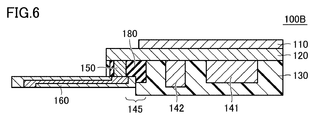
- FIG. 6 is a cross-sectional view of the electronic device 100B of the second modification.
- the electronic device 100B has a configuration in which the periphery of the conductive portion 150 and the boundary portion 145 of the mold layer 130 are covered with a resin 180 having a higher elastic modulus than the sealing resin material of the mold layer 130.
- the resin 180 is exposed at the portion 172. That is, since the resin 180 has higher rigidity than the sealing resin material of the mold layer 130, higher durability can be realized against stress acting on the corner portion 172.
- an inorganic filler mixed resin in which an inorganic filler such as silica or alumina is mixed can be used.
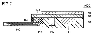
- FIG. 7 is a cross-sectional view of the electronic device 100 ⁇ / b> C of the third modification.
- electronic device 100C contrary to Modification 2, the periphery of conductive portion 150 and the boundary portion 145 of mold layer 130 are covered with resin 182 having a lower elastic modulus than the sealing resin material of mold layer 130.
- the resin 180 is exposed at the corner portion 172. That is, the resin 182 has higher flexibility than the sealing resin material of the mold layer 130 and is easily elastically deformed. Therefore, even when a stress is applied to the corner portion 172, the resin 182 is elastically deformed to absorb the stress like a cushion, so that the corner portion 172 is prevented from being damaged. Therefore, durability higher than that of the sealing resin material can be realized against stress acting on the corner portion 172.
- low elastic material for example, polyimide, bismaleimide, polyamide, polyamideimide, polybenzoxazole, benzocyclobutene, aramid resin, silicone resin, liquid crystal polymer and the like can be used.
- Modifications 2 and 3 are the same as those in FIG. 3B of the manufacturing process illustrated in FIG. 3, in which the resin 180 (or the resin 182) is formed before the mold layer 130 is formed of the sealing resin material. It can be formed by partially molding only the periphery of the conductive part 150 and then molding the whole with a sealing resin material.
- the wiring pattern formed of a metal material such as copper and the insulating layer formed of a resin have different elastic modulus or density, and also have different ultrasonic reflectivity. As shown in FIG. 8, when the wiring pattern is arranged on the second surface 122 of the wiring board 120, that is, immediately below the sensor board 110, when the user touches the sensor board 110 with a finger, A force is applied in the direction of AR1.
- the density is different between the portion where the wiring pattern 125 is disposed and the resin portion where the wiring pattern 125 is not present. Will be added.
- the sensor substrate 110 itself is partially distorted, and the ultrasonic attenuation state may be nonuniform on the detection surface of the sensor substrate 110.
- the wiring pattern 125 when the wiring pattern 125 is disposed immediately below the sensor substrate 110, ultrasonic waves are generated between a portion where the sensor substrate 110 and the wiring pattern 125 are in contact with each other and a portion where the sensor substrate 110 and the resin are in contact with each other.
- the reflection state can be non-uniform.
- the reflection state of the ultrasonic wave differs depending on the presence or absence of the wiring pattern 125, the image of the wiring pattern 125 may be reflected in the detected fingerprint image.
- the wiring pattern 125 is not disposed in the portion (second surface 122) immediately below the sensor board 110, and the sensor board 110 and the wiring pattern 125 are not in contact with each other. It is preferable to do.
- the wiring pattern 125 is formed in the inner layer of the wiring substrate 120, and at least one insulating layer is formed between the sensor substrate 110 and the wiring pattern 125.
- an intermediate layer 127 of metal or other insulating material is disposed in a layer between the sensor substrate 110 and the wiring pattern 125 so as to block the wiring pattern 125. You may make it make the reflection of an ultrasonic wave uniform.
- the wiring pattern 125 When it is necessary to form the wiring pattern 125 on the second surface 122 of the wiring board 120, the wiring pattern 125 is covered with an intermediate layer 128 of metal or other insulating material as shown in FIG.
- the sensor substrate 110 may be disposed on the intermediate layer 128.
- 10 fingerprint authentication device 20 housing, 50 support, 100, 100A to 100C electronic device, 110 sensor substrate, 120 wiring substrate, 121 first surface, 122 second surface, 125, 162 wiring pattern, 127, 128 intermediate layer , 130 mold layer, 131 thick part, 132 thin part, 135 back surface, 140 built-in equipment, 141 integrated circuit, 142 capacitor, 145 boundary part, 150, 150A conductive part, 160 terminal board, 161, 163 terminal, 170 step part , 172 corner, 173 exposed surface, 180,182 resin.
Abstract
L'invention concerne un dispositif électronique (100) comprenant : un premier substrat (120) présentant un motif de câblage formé à l'intérieur de ce dernier ; un second substrat (160) possédant une borne externe formée sur ce dernier ; un premier équipement électronique (141) disposé sur une première surface du premier substrat ; un second équipement électronique (110) disposé sur une seconde surface du premier substrat ; une couche de moule (130) permettant de mouler le premier équipement électronique ; et une partie conductrice (150) disposée à l'intérieur de la couche de moule. Le second équipement électronique est connecté électriquement au premier équipement électronique. La partie conductrice connecte électriquement le premier substrat et le second substrat. La couche de moule comprend, formée à une extrémité de cette dernière, une partie étagée (170) où la partie conductrice est exposée. Le second substrat est disposé au niveau de la partie étagée. La distance dans la direction de l'épaisseur entre le second substrat et le premier substrat est plus courte que la distance entre la première surface du premier substrat et une surface du premier équipement électronique sur le côté opposé au premier substrat.
Priority Applications (3)
| Application Number | Priority Date | Filing Date | Title |
|---|---|---|---|
| CN201980019503.4A CN111886623B (zh) | 2018-05-01 | 2019-02-28 | 电子设备以及搭载了该电子设备的指纹认证装置 |
| JP2020517025A JP6784342B2 (ja) | 2018-05-01 | 2019-02-28 | 電子デバイスおよびそれを搭載した指紋認証装置 |
| US17/062,864 US10997389B2 (en) | 2018-05-01 | 2020-10-05 | Electronic device with exposed conductive member at step in mold and fingerprint recognition apparatus equipped with the same |
Applications Claiming Priority (2)
| Application Number | Priority Date | Filing Date | Title |
|---|---|---|---|
| JP2018088117 | 2018-05-01 | ||
| JP2018-088117 | 2018-05-01 |
Related Child Applications (1)
| Application Number | Title | Priority Date | Filing Date |
|---|---|---|---|
| US17/062,864 Continuation US10997389B2 (en) | 2018-05-01 | 2020-10-05 | Electronic device with exposed conductive member at step in mold and fingerprint recognition apparatus equipped with the same |
Publications (1)
| Publication Number | Publication Date |
|---|---|
| WO2019211941A1 true WO2019211941A1 (fr) | 2019-11-07 |
Family
ID=68386524
Family Applications (1)
| Application Number | Title | Priority Date | Filing Date |
|---|---|---|---|
| PCT/JP2019/007780 WO2019211941A1 (fr) | 2018-05-01 | 2019-02-28 | Dispositif électronique et dispositif d'authentification d'empreintes digitales comprenant ce dernier |
Country Status (4)
| Country | Link |
|---|---|
| US (1) | US10997389B2 (fr) |
| JP (1) | JP6784342B2 (fr) |
| CN (1) | CN111886623B (fr) |
| WO (1) | WO2019211941A1 (fr) |
Citations (5)
| Publication number | Priority date | Publication date | Assignee | Title |
|---|---|---|---|---|
| JP2003235830A (ja) * | 2002-02-20 | 2003-08-26 | Fujitsu Ltd | 指紋センサ装置及びその製造方法 |
| JP2005242841A (ja) * | 2004-02-27 | 2005-09-08 | Casio Comput Co Ltd | 電子機器 |
| JP2013534008A (ja) * | 2010-06-18 | 2013-08-29 | オーセンテック,インコーポレイテッド | センシングエリア上に封止層を有する指センサおよび関連する方法 |
| JP2013541773A (ja) * | 2010-10-08 | 2013-11-14 | アップル インコーポレイテッド | 差動測定回路を含む指検出デバイス及び関連する方法 |
| JP2017511162A (ja) * | 2014-01-29 | 2017-04-20 | サムスン エレクトロニクス カンパニー リミテッド | 指紋認識装置とその製造方法および電子機器 |
Family Cites Families (31)
| Publication number | Priority date | Publication date | Assignee | Title |
|---|---|---|---|---|
| US6551248B2 (en) | 2001-07-31 | 2003-04-22 | Koninklijke Philips Electronics N.V. | System for attaching an acoustic element to an integrated circuit |
| JP3612312B2 (ja) | 2002-07-19 | 2005-01-19 | アロカ株式会社 | 超音波探触子及びその製造方法 |
| WO2004072576A1 (fr) * | 2003-02-17 | 2004-08-26 | Nippon Telegraph And Telephone Corporation | Capteur de reconnaissance de la forme d'une surface et son procede de production |
| WO2007047816A1 (fr) * | 2005-10-18 | 2007-04-26 | Authentec, Inc. | Capteur d'empreinte digitale comprenant un circuit souple, et methodes associees |
| JP2009061112A (ja) | 2007-09-06 | 2009-03-26 | Ge Medical Systems Global Technology Co Llc | 超音波探触子および超音波撮像装置 |
| JP2011044452A (ja) * | 2009-08-19 | 2011-03-03 | Denso Corp | 電子装置およびその製造方法 |
| KR101867106B1 (ko) * | 2010-03-30 | 2018-06-12 | 다이니폰 인사츠 가부시키가이샤 | Led용 수지 부착 리드 프레임, 반도체 장치, 반도체 장치의 제조 방법 및 led용 수지 부착 리드 프레임의 제조 방법 |
| US9001040B2 (en) * | 2010-06-02 | 2015-04-07 | Synaptics Incorporated | Integrated fingerprint sensor and navigation device |
| US9065358B2 (en) * | 2011-07-11 | 2015-06-23 | Taiwan Semiconductor Manufacturing Company, Ltd. | MEMS structure and method of forming same |
| CN204808363U (zh) * | 2012-11-20 | 2015-11-25 | 韩国科泰高科株式会社 | 指纹传感器模块、具有此的便携式电子设备 |
| JP5743040B2 (ja) * | 2013-05-13 | 2015-07-01 | 株式会社村田製作所 | フレキシブル回路基板、および、フレキシブル回路基板の製造方法 |
| JP2015005263A (ja) * | 2013-05-20 | 2015-01-08 | 日東電工株式会社 | センサ基板 |
| KR20150018350A (ko) * | 2013-08-08 | 2015-02-23 | 삼성전자주식회사 | 지문인식장치와 그 제조방법 및 전자기기 |
| JP2016048723A (ja) * | 2014-08-27 | 2016-04-07 | イビデン株式会社 | フレックスリジッド配線板 |
| JP6288294B2 (ja) * | 2014-10-31 | 2018-03-07 | 株式会社村田製作所 | アンテナモジュール及び回路モジュール |
| CN207529410U (zh) * | 2015-02-27 | 2018-06-22 | 株式会社村田制作所 | Rfic设备 |
| JP5997796B2 (ja) | 2015-02-27 | 2016-09-28 | 株式会社日立製作所 | 超音波振動子ユニット |
| US10134966B2 (en) * | 2015-02-27 | 2018-11-20 | Nichia Corporation | Light emitting device |
| WO2016204208A1 (fr) * | 2015-06-19 | 2016-12-22 | 株式会社村田製作所 | Module et son procédé de fabrication |
| US10055631B1 (en) * | 2015-11-03 | 2018-08-21 | Synaptics Incorporated | Semiconductor package for sensor applications |
| US20200328143A1 (en) * | 2016-04-29 | 2020-10-15 | Uniqarta, Inc. | Connecting electronic components to substrates |
| US10354114B2 (en) * | 2016-06-13 | 2019-07-16 | Taiwan Semiconductor Manufacturing Company, Ltd. | Fingerprint sensor in InFO structure and formation method |
| US9691708B1 (en) * | 2016-07-20 | 2017-06-27 | Taiwan Semiconductor Manufacturing Co., Ltd. | Semiconductor package and manufacturing method thereof |
| KR102279735B1 (ko) * | 2016-10-10 | 2021-07-20 | 삼성전자주식회사 | 전자 장치 및 그 제작 방법 |
| JP6815159B2 (ja) * | 2016-10-14 | 2021-01-20 | 株式会社ジャパンディスプレイ | 表示装置 |
| US10978403B2 (en) * | 2019-01-30 | 2021-04-13 | Delta Electronics, Inc. | Package structure and method for fabricating the same |
| JP6724851B2 (ja) * | 2017-04-14 | 2020-07-15 | 株式会社デンソー | 基材、それを用いたモールドパーケージ、基材の製造方法、およびモールドパッケージの製造方法 |
| CN111357395B (zh) * | 2017-11-20 | 2022-03-11 | 株式会社村田制作所 | 高频模块 |
| DE112017008339T5 (de) * | 2017-12-30 | 2020-09-10 | Intel Corporation | Null-fehlausrichtungs-zwei-via-strukturen, verwendend ein photobildbares dielektrikum, einen aufbaufilm und elektrolytisches plattieren |
| KR102478310B1 (ko) * | 2018-12-05 | 2022-12-16 | 삼성전자주식회사 | 도전성 패턴이 형성된 힌지 하우징을 포함하는 전자 장치 |
| TWI732228B (zh) * | 2019-02-19 | 2021-07-01 | 美律實業股份有限公司 | 麥克風封裝結構 |
-
2019
- 2019-02-28 CN CN201980019503.4A patent/CN111886623B/zh active Active
- 2019-02-28 WO PCT/JP2019/007780 patent/WO2019211941A1/fr active Application Filing
- 2019-02-28 JP JP2020517025A patent/JP6784342B2/ja active Active
-
2020
- 2020-10-05 US US17/062,864 patent/US10997389B2/en active Active
Patent Citations (5)
| Publication number | Priority date | Publication date | Assignee | Title |
|---|---|---|---|---|
| JP2003235830A (ja) * | 2002-02-20 | 2003-08-26 | Fujitsu Ltd | 指紋センサ装置及びその製造方法 |
| JP2005242841A (ja) * | 2004-02-27 | 2005-09-08 | Casio Comput Co Ltd | 電子機器 |
| JP2013534008A (ja) * | 2010-06-18 | 2013-08-29 | オーセンテック,インコーポレイテッド | センシングエリア上に封止層を有する指センサおよび関連する方法 |
| JP2013541773A (ja) * | 2010-10-08 | 2013-11-14 | アップル インコーポレイテッド | 差動測定回路を含む指検出デバイス及び関連する方法 |
| JP2017511162A (ja) * | 2014-01-29 | 2017-04-20 | サムスン エレクトロニクス カンパニー リミテッド | 指紋認識装置とその製造方法および電子機器 |
Also Published As
| Publication number | Publication date |
|---|---|
| CN111886623B (zh) | 2024-05-07 |
| JPWO2019211941A1 (ja) | 2020-12-10 |
| CN111886623A (zh) | 2020-11-03 |
| US10997389B2 (en) | 2021-05-04 |
| US20210019490A1 (en) | 2021-01-21 |
| JP6784342B2 (ja) | 2020-11-11 |
Similar Documents
| Publication | Publication Date | Title |
|---|---|---|
| US20210373709A1 (en) | Fingerprint sensor and button combinations and methods of making same | |
| US9960512B2 (en) | Flexible circuit board and device | |
| US10242242B2 (en) | Semiconductor fingerprint identification sensor and manufacturing method thereof | |
| US7019375B2 (en) | Solid-state imaging apparatus and manufacturing method thereof | |
| US8149001B2 (en) | Low cost fingerprint sensor system | |
| CN109427731B (zh) | 电路基板 | |
| KR102144933B1 (ko) | 칩 패키지 및 그 제조방법 | |
| WO2014002860A1 (fr) | Module de caméra et dispositif électronique | |
| CN109429431B (zh) | 电路基板 | |
| TWI755555B (zh) | 印刷電路板以及具有印刷電路板的電子裝置 | |
| WO2019211941A1 (fr) | Dispositif électronique et dispositif d'authentification d'empreintes digitales comprenant ce dernier | |
| JP2012182274A (ja) | モジュール部品、その製造方法、及びそれが実装された半導体パッケージ、電子モジュール、または電子機器 | |
| JP2008153478A (ja) | プリント配線基板、その製造方法および電子機器 | |
| JP5427476B2 (ja) | 半導体センサ装置 | |
| WO2014123556A1 (fr) | Dispositif à ultrasons | |
| KR20190089406A (ko) | 지문 인식 장치 및 이를 포함하는 전자 디바이스 | |
| KR102561936B1 (ko) | 인쇄회로기판 | |
| US20070230146A1 (en) | Printed-wiring board with built-in component, manufacturing method of printed-wiring board with built-in component, and electronic device | |
| US11439011B2 (en) | Electronic device module and method of manufacturing electronic device module | |
| KR101008479B1 (ko) | 경연성 인쇄회로기판 및 그 제조방법 | |
| KR101969643B1 (ko) | 리지드 플렉시블 회로기판 제조방법 | |
| US20220201839A1 (en) | Dielectric material change to optimize electrical and mechanical properties of flex circuit | |
| US20090109642A1 (en) | Semiconductor modules and electronic devices using the same | |
| KR20160084143A (ko) | 전자소자 내장기판 및 그 제조 방법 | |
| KR20220083188A (ko) | 안테나 패키지 및 이를 포함하는 화상 표시 장치 |
Legal Events
| Date | Code | Title | Description |
|---|---|---|---|
| 121 | Ep: the epo has been informed by wipo that ep was designated in this application |
Ref document number: 19796608 Country of ref document: EP Kind code of ref document: A1 |
|
| ENP | Entry into the national phase |
Ref document number: 2020517025 Country of ref document: JP Kind code of ref document: A |
|
| NENP | Non-entry into the national phase |
Ref country code: DE |
|
| 122 | Ep: pct application non-entry in european phase |
Ref document number: 19796608 Country of ref document: EP Kind code of ref document: A1 |