WO2019188249A1 - 半導体記憶装置及び積和演算装置 - Google Patents
半導体記憶装置及び積和演算装置 Download PDFInfo
- Publication number
- WO2019188249A1 WO2019188249A1 PCT/JP2019/009982 JP2019009982W WO2019188249A1 WO 2019188249 A1 WO2019188249 A1 WO 2019188249A1 JP 2019009982 W JP2019009982 W JP 2019009982W WO 2019188249 A1 WO2019188249 A1 WO 2019188249A1
- Authority
- WO
- WIPO (PCT)
- Prior art keywords
- memory device
- semiconductor memory
- ferroelectric
- gate electrode
- semiconductor
- Prior art date
- Legal status (The legal status is an assumption and is not a legal conclusion. Google has not performed a legal analysis and makes no representation as to the accuracy of the status listed.)
- Ceased
Links
Images












Classifications
-
- H—ELECTRICITY
- H10—SEMICONDUCTOR DEVICES; ELECTRIC SOLID-STATE DEVICES NOT OTHERWISE PROVIDED FOR
- H10B—ELECTRONIC MEMORY DEVICES
- H10B53/00—Ferroelectric RAM [FeRAM] devices comprising ferroelectric memory capacitors
- H10B53/30—Ferroelectric RAM [FeRAM] devices comprising ferroelectric memory capacitors characterised by the memory core region
-
- H—ELECTRICITY
- H10—SEMICONDUCTOR DEVICES; ELECTRIC SOLID-STATE DEVICES NOT OTHERWISE PROVIDED FOR
- H10B—ELECTRONIC MEMORY DEVICES
- H10B12/00—Dynamic random access memory [DRAM] devices
- H10B12/30—DRAM devices comprising one-transistor - one-capacitor [1T-1C] memory cells
- H10B12/36—DRAM devices comprising one-transistor - one-capacitor [1T-1C] memory cells the transistor being a FinFET
-
- H—ELECTRICITY
- H10—SEMICONDUCTOR DEVICES; ELECTRIC SOLID-STATE DEVICES NOT OTHERWISE PROVIDED FOR
- H10B—ELECTRONIC MEMORY DEVICES
- H10B51/00—Ferroelectric RAM [FeRAM] devices comprising ferroelectric memory transistors
- H10B51/30—Ferroelectric RAM [FeRAM] devices comprising ferroelectric memory transistors characterised by the memory core region
-
- H—ELECTRICITY
- H10—SEMICONDUCTOR DEVICES; ELECTRIC SOLID-STATE DEVICES NOT OTHERWISE PROVIDED FOR
- H10B—ELECTRONIC MEMORY DEVICES
- H10B53/00—Ferroelectric RAM [FeRAM] devices comprising ferroelectric memory capacitors
- H10B53/10—Ferroelectric RAM [FeRAM] devices comprising ferroelectric memory capacitors characterised by the top-view layout
-
- H—ELECTRICITY
- H10—SEMICONDUCTOR DEVICES; ELECTRIC SOLID-STATE DEVICES NOT OTHERWISE PROVIDED FOR
- H10D—INORGANIC ELECTRIC SEMICONDUCTOR DEVICES
- H10D30/00—Field-effect transistors [FET]
- H10D30/60—Insulated-gate field-effect transistors [IGFET]
-
- H—ELECTRICITY
- H10—SEMICONDUCTOR DEVICES; ELECTRIC SOLID-STATE DEVICES NOT OTHERWISE PROVIDED FOR
- H10D—INORGANIC ELECTRIC SEMICONDUCTOR DEVICES
- H10D64/00—Electrodes of devices having potential barriers
- H10D64/20—Electrodes characterised by their shapes, relative sizes or dispositions
- H10D64/27—Electrodes not carrying the current to be rectified, amplified, oscillated or switched, e.g. gates
- H10D64/311—Gate electrodes for field-effect devices
- H10D64/411—Gate electrodes for field-effect devices for FETs
- H10D64/511—Gate electrodes for field-effect devices for FETs for IGFETs
- H10D64/512—Disposition of the gate electrodes, e.g. buried gates
-
- H—ELECTRICITY
- H10—SEMICONDUCTOR DEVICES; ELECTRIC SOLID-STATE DEVICES NOT OTHERWISE PROVIDED FOR
- H10D—INORGANIC ELECTRIC SEMICONDUCTOR DEVICES
- H10D84/00—Integrated devices formed in or on semiconductor substrates that comprise only semiconducting layers, e.g. on Si wafers or on GaAs-on-Si wafers
-
- H—ELECTRICITY
- H10—SEMICONDUCTOR DEVICES; ELECTRIC SOLID-STATE DEVICES NOT OTHERWISE PROVIDED FOR
- H10D—INORGANIC ELECTRIC SEMICONDUCTOR DEVICES
- H10D84/00—Integrated devices formed in or on semiconductor substrates that comprise only semiconducting layers, e.g. on Si wafers or on GaAs-on-Si wafers
- H10D84/01—Manufacture or treatment
- H10D84/0123—Integrating together multiple components covered by H10D12/00 or H10D30/00, e.g. integrating multiple IGBTs
- H10D84/0126—Integrating together multiple components covered by H10D12/00 or H10D30/00, e.g. integrating multiple IGBTs the components including insulated gates, e.g. IGFETs
-
- H—ELECTRICITY
- H10—SEMICONDUCTOR DEVICES; ELECTRIC SOLID-STATE DEVICES NOT OTHERWISE PROVIDED FOR
- H10D—INORGANIC ELECTRIC SEMICONDUCTOR DEVICES
- H10D84/00—Integrated devices formed in or on semiconductor substrates that comprise only semiconducting layers, e.g. on Si wafers or on GaAs-on-Si wafers
- H10D84/01—Manufacture or treatment
- H10D84/02—Manufacture or treatment characterised by using material-based technologies
- H10D84/03—Manufacture or treatment characterised by using material-based technologies using Group IV technology, e.g. silicon technology or silicon-carbide [SiC] technology
- H10D84/038—Manufacture or treatment characterised by using material-based technologies using Group IV technology, e.g. silicon technology or silicon-carbide [SiC] technology using silicon technology, e.g. SiGe
Definitions
- the present disclosure relates to a semiconductor memory device and a product-sum operation device.
- FeRAM Feroelectric Random Access Memory
- a lower electrode, a ferroelectric film, and an upper electrode are sequentially stacked on a gate electrode of a MIS (Metal-Insulator-Semiconductor) type field effect transistor formed on a semiconductor substrate.
- MIS Metal-Insulator-Semiconductor
- a structure for forming a ferroelectric capacitor is known.
- Such a structure is also referred to as a MFMIS (Metal-Ferroelectric-Metal-Insulator-Semiconductor) structure.
- one end of the MFMIS structure FeRAM is connected between the gate electrode of the MIS field effect transistor and the lower electrode of the ferroelectric capacitor, and the other end is the source of the MIS field effect transistor.
- a technique for increasing the distribution voltage of the ferroelectric capacitor by further providing a paraelectric capacitor connected to the capacitor is disclosed.
- Patent Document 1 it is necessary to further provide a region where a paraelectric capacitor is formed on a semiconductor substrate, so that the area per unit cell of FeRAM becomes large. Therefore, the FeRAM disclosed in Patent Document 1 has been difficult to be highly integrated.
- the present disclosure proposes a new and improved semiconductor memory device and product-sum operation device that can apply a sufficient voltage to a ferroelectric capacitor and has a structure suitable for high integration. .
- a ferroelectric capacitor formed by sandwiching a ferroelectric material between a transistor and a pair of conductive materials, wherein one of the conductive materials is electrically connected to the gate electrode of the transistor; And a channel of the transistor is formed three-dimensionally over a plurality of surfaces.
- a ferroelectric capacitor is formed by sandwiching a ferroelectric material between a transistor and a pair of conductive materials, and one of the conductive materials is electrically connected to the gate electrode of the transistor
- the product-sum operation device is provided in which the channel of the transistor is three-dimensionally formed across a plurality of surfaces.
- the ferroelectric capacitor is formed by sandwiching a ferroelectric material between a transistor and a pair of conductive materials, and one of the conductive materials is electrically connected to the gate electrode of the transistor. And the pair of conductive materials and the ferroelectric material are stacked in parallel with the upper surface of the gate electrode, so that the ferroelectric capacitor is provided on the gate electrode, A semiconductor memory device is provided in which the planar area of the ferroelectric capacitor is smaller than the planar area of the upper surface of the gate electrode.
- a ferroelectric capacitor formed by sandwiching a ferroelectric material between a transistor and a pair of conductive materials, wherein one of the conductive materials is electrically connected to the gate electrode of the transistor. And the pair of conductive materials and the ferroelectric material are stacked in parallel with the upper surface of the gate electrode, so that the ferroelectric capacitor is provided on the gate electrode, A product-sum operation device is provided in which the planar area of the ferroelectric capacitor is smaller than the planar area of the upper surface of the gate electrode.
- the semiconductor memory device increases the gate capacitance of the field effect transistor without increasing the size of the unit cell, thereby reducing the distribution voltage applied to the ferroelectric film of the ferroelectric capacitor. Can be higher.
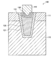
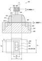
- FIG. 3 is a longitudinal sectional view schematically showing a structure example of a semiconductor memory device according to the first embodiment of the present disclosure.
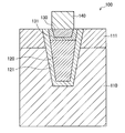
- FIG. It is a longitudinal cross-sectional view which shows typically the structure which concerns on the modification of a semiconductor memory device. It is a longitudinal cross-sectional view which shows typically the structure which concerns on the modification of a semiconductor memory device.
- FIG. 2 is a longitudinal sectional view defining dimensions of each component of the semiconductor memory device shown in FIG.
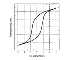
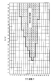
- FIG. 6 is a graph showing a range in which the characteristics of the semiconductor memory device according to the same embodiment are good.
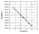
- FIG. 6 is a graph showing a range in which the characteristics of the semiconductor memory device according to the same embodiment are good.
- FIG. 6 is a graph showing a range in which the characteristics of the semiconductor memory device according to the same embodiment are good.
- FIG. 6 is a graph showing a range in which the characteristics of the semiconductor memory device according to the same embodiment are good.
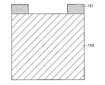
- FIG. 6 is a schematic longitudinal sectional view showing a step of the method of manufacturing the semiconductor memory device according to the same embodiment.
- FIG. 6 is a schematic longitudinal sectional view showing a step of the method of manufacturing the semiconductor memory device according to the same embodiment.
- FIG. 6 is a schematic longitudinal sectional view showing a step of the method of manufacturing the semiconductor memory device according to the same embodiment.
- FIG. 6 is a schematic longitudinal sectional view showing a step of the method of manufacturing the semiconductor memory device according to the same embodiment.
- FIG. 6 is a schematic longitudinal sectional view showing a step of the method of manufacturing the semiconductor memory device according to the same embodiment.
- FIG. 6 is a schematic longitudinal sectional view showing a step of the method of manufacturing the semiconductor memory device according to the same embodiment.
- FIG. 6 is a schematic longitudinal sectional view showing a step of the method of manufacturing the semiconductor memory device according to the same embodiment.
- FIG. 6 is a schematic longitudinal sectional view showing a step of the method of manufacturing the semiconductor memory device according to the same embodiment.
- 2 is a plan view schematically showing a planar configuration of a semiconductor device in which a plurality of semiconductor memory devices according to the embodiment are arranged in a matrix.
- FIG. 7 is a longitudinal sectional view schematically showing a cross section of the semiconductor device shown in FIG.
- FIG. 8 is an equivalent circuit diagram of the semiconductor device shown in FIGS. 6 and 7. It is a longitudinal cross-sectional view typically shown in the cross-sectional structure which concerns on the modification of a semiconductor device.
- FIG. 6 is a schematic longitudinal sectional view showing a step of the method of manufacturing the semiconductor memory device according to the same embodiment.
- FIG. 6 is a schematic longitudinal sectional view showing a step of the method of manufacturing the semiconductor memory device according to the same embodiment.
- 2 is a
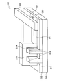
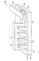
- FIG. 6 is a perspective view schematically illustrating a structure example of a semiconductor memory device according to a second embodiment of the present disclosure. It is a longitudinal cross-sectional view which shows typically the structure which concerns on the modification of a semiconductor memory device. It is a longitudinal cross-sectional view which shows typically the structure which concerns on the modification of a semiconductor memory device. It is a longitudinal cross-sectional view which shows typically the structure which concerns on the modification of a semiconductor memory device. It is a longitudinal cross-sectional view which shows typically the structure which concerns on the modification of a semiconductor memory device.
- FIG. 11 is a perspective view defining dimensions of each component of the semiconductor memory device shown in FIG. 10.
- FIG. 2 is a plan view schematically showing a planar configuration of a semiconductor device in which a plurality of semiconductor memory devices according to the embodiment are arranged in a matrix.
- FIG. 2 is a longitudinal sectional view schematically showing a structural example of a semiconductor memory device according to the same embodiment.
- FIG. FIG. 15 is a longitudinal sectional view defining dimensions of each component of the semiconductor memory device shown in FIG. 14.
- FIG. 6 is a schematic longitudinal sectional view showing a step of the method of manufacturing the semiconductor memory device according to the same embodiment.
- FIG. 6 is a schematic longitudinal sectional view showing a step of the method of manufacturing the semiconductor memory device according to the same embodiment.
- FIG. 6 is a schematic longitudinal sectional view showing a step of the method of manufacturing the semiconductor memory device according to the same embodiment.
- FIG. 6 is a schematic longitudinal sectional view showing a step of the method of manufacturing the semiconductor memory device according to the same embodiment.
- FIG. 6 is a schematic longitudinal sectional view showing a step of the method of manufacturing the semiconductor memory device according to the same embodiment.
- FIG. 6 is a schematic longitudinal sectional view showing a step of the method of manufacturing the semiconductor memory device according to the same embodiment.
- It is a longitudinal cross-sectional view which shows typically the structure which concerns on the modification of a semiconductor memory device.
- It is a longitudinal cross-sectional view which shows typically the structure which concerns on the modification of a semiconductor memory device.
- It is a longitudinal cross-sectional view which shows typically the structure which concerns on the modification of a semiconductor memory device.
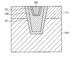
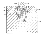
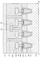
- FIG. 1 is a longitudinal sectional view schematically showing a structural example of the semiconductor memory device according to this embodiment.
- a semiconductor memory device 100 includes a semiconductor substrate 110, a source or drain region 111, a gate insulating film 121, a lower electrode 120, a ferroelectric film 131, an upper electrode 130, and a conductor electrode. 140.
- the semiconductor memory device 100 is an FeRAM having an MFMIS structure in which a ferroelectric capacitor is connected in series on a gate electrode of a field effect transistor.
- the field effect transistor is formed by the semiconductor substrate 110, the source or drain region 111, the gate insulating film 121, and the lower electrode 120
- the ferroelectric capacitor is formed by the lower electrode 120, the ferroelectric film 131, and the upper electrode. 130.
- the ferroelectric capacitor is connected in series with the gate of the field effect transistor at the lower electrode 120.
- the semiconductor substrate 110 is a substrate made of a semiconductor material.
- a first conductivity type impurity (for example, a p-type impurity such as boron or aluminum) is introduced into the semiconductor substrate 110 in a region where the semiconductor memory device 100 is formed.
- the semiconductor substrate 110 may be a silicon substrate or an SOI (Silicon On Insulator) substrate in which an insulating film such as SiO 2 is sandwiched between silicon substrates.
- the semiconductor substrate 110 is a substrate formed of another elemental semiconductor such as germanium, or a substrate formed of a compound semiconductor such as gallium arsenide (GaAs), gallium nitride (GaN), or silicon carbide (SiC). Also good.
- the semiconductor substrate 110 may be a substrate in which a semiconductor layer is stacked on a substrate made of quartz, sapphire, resin, metal, or the like.
- the source or drain region 111 is a second conductivity type (for example, n-type) region formed in the semiconductor substrate 110. Specifically, the source or drain region 111 is provided by introducing a second conductivity type impurity (for example, an n-type impurity such as phosphorus or arsenic) into regions on both sides of the opening provided in the semiconductor substrate 110. . A field effect transistor and a ferroelectric capacitor are formed inside the opening provided in the semiconductor substrate 110. Note that the source or drain regions 111 are not necessarily provided on both sides of the opening provided in the semiconductor substrate 110 as long as they are separated from each other.
- a second conductivity type impurity for example, an n-type impurity such as phosphorus or arsenic
- either the source or drain region 111 formed on both sides of the opening provided in the semiconductor substrate 110 may function as a source region, and any of them may function as a drain region. These can be arbitrarily changed by the wiring connected to each of the source or drain regions 111.
- the gate insulating film 121 is made of an insulating material and is provided along the internal shape of the opening formed in the semiconductor substrate 110. Specifically, the opening formed in the semiconductor substrate 110 is provided up to a region deeper than the source or drain region 111 of the semiconductor substrate 110, and the gate insulating film 121 is provided along the bottom and side surfaces of the opening.
- the gate insulating film 121 may be formed of a known insulating material as a gate insulating film of a field effect transistor.
- the gate insulating film 121 may be formed of an insulating oxynitride such as silicon oxide (SiO x ), silicon nitride (SiN x ), or silicon oxynitride (SiON).
- the lower electrode 120 is made of a conductive material, and is provided on the gate insulating film 121 so as to embed an opening formed in the semiconductor substrate 110.
- the lower electrode 120 may be formed of polysilicon or the like, and may be formed of a metal, an alloy, or a metal compound. Note that the lower electrode 120 is not electrically connected to another wiring and is provided in a state where the potential is independent (a so-called floating state).
- the ferroelectric film 131 is made of a ferroelectric material and is provided along the internal shape of the opening provided in the lower electrode 120. Specifically, the opening provided in the lower electrode 120 is provided inside the lower electrode 120, and the ferroelectric film 131 is provided along the bottom and side surfaces of the opening. Note that the opening provided in the lower electrode 120 may be provided so as to expose the gate insulating film 121.
- the ferroelectric film 131 is formed of a ferroelectric material that spontaneously polarizes and whose remanent polarization direction can be controlled by an external electric field.
- the ferroelectric film 131 is formed of a ferroelectric material containing hafnium (Hf), zirconium (Zr), silicon (Si), or oxygen (O).
- the ferroelectric film 131 is a ferroelectric material having a perovskite structure such as lead zirconate titanate (Pb (Zr, Ti) O 3 : PZT) or strontium bistrontate tantalate (SrBi 2 Ta 2 O 9 : SBT). It may be made of a material.
- the ferroelectric film 131 may be a ferroelectric film obtained by modifying a film made of a high dielectric material such as HfO x , ZrO x or HfZrO x by heat treatment or the like. It may be a ferroelectric film modified by introducing atoms such as lanthanum (La), silicon (Si), or gadolinium (Gd) into the resulting film. Further, the ferroelectric film 131 may be formed of a single layer or a plurality of layers. For example, the ferroelectric film 131 may be a single layer film made of a ferroelectric material such as HfO x .
- the upper electrode 130 is made of a conductive material, and is provided on the ferroelectric film 131 so as to fill the opening formed in the lower electrode 120.
- the upper electrode 130 may be formed of a metal such as titanium (Ti) or tungsten (W), or a metal compound such as titanium nitride (TiN) or tantalum nitride (TaN).
- the conductor electrode 140 is made of a conductive material and is provided on the upper electrode 130. However, the conductor electrode 140 is provided in a size that does not contact the lower electrode 120 in order to place the lower electrode 120 in a floating state. For example, the conductor electrode 140 functions as a connection terminal of the semiconductor memory device 100 by being electrically connected to another wiring in an upper layer than the semiconductor substrate 110.
- the conductor electrode 140 may be formed of a metal material such as copper (Cu) or aluminum (Al), for example.
- the semiconductor memory device 100 may have the structure shown in FIGS. 2A and 2B.
- 2A and 2B are longitudinal sectional views schematically showing a structure according to a modified example of the semiconductor memory device 100.
- FIG. 2A and 2B are longitudinal sectional views schematically showing a structure according to a modified example of the semiconductor memory device 100.
- the conductor electrode 141 may be provided on the upper electrode 130 so as to fill the opening provided in the lower electrode 120. That is, the conductor electrode 141 may not be provided on the surface of the semiconductor substrate 110, but may be provided so that a part of the conductor electrode 141 is embedded inside the semiconductor substrate 110.
- the material etc. which comprise the conductor electrode 141 since it is substantially the same as that of the conductor electrode 140, description here is abbreviate
- the opening provided in the lower electrode 120 is provided so as to expose the gate insulating film 121, and the ferroelectric film 131 is in contact with the gate insulating film 121. It may be provided.
- the opening provided in the lower electrode 120 causes the lower electrode 120 to recede (recess) from the surface of the semiconductor substrate 110, and the ferroelectric film 131 and the upper electrode 130 are formed in the recessed region of the lower electrode 120. May be.
- the lower electrode 120 that is in a floating state is not exposed on the surface of the semiconductor substrate 110. Therefore, the conductor electrode 141 can be formed in any size without considering the possibility of contacting the lower electrode 120.
- the semiconductor memory device 100 by applying a voltage V between the upper electrode 130 and the source or drain region 111, the ferroelectric film 131 of the ferroelectric capacitor, and the gate of the field effect transistor. A voltage is applied to the insulating film 121. At this time, a voltage inversely proportional to the ratio of the capacitance Cf of the ferroelectric capacitor and the gate capacitance Ci of the field effect transistor is applied to the ferroelectric film 131 and the gate insulating film 121.
- the distribution voltage Vf applied to the ferroelectric film 131 depends on the coupling ratio (Ci / (Ci + Cf)) between the capacitance Cf of the ferroelectric capacitor and the gate capacitance Ci of the field effect transistor.
- the dielectric constant of the ferroelectric film 131 formed of a ferroelectric material is higher than that of the gate insulating film 121 formed of an insulating material. Therefore, when the areas of the ferroelectric film 131 and the gate insulating film 121 are the same, the capacitance Cf of the ferroelectric capacitor is larger than the gate capacitance Ci of the field effect transistor. In such a case, most of the voltage V applied between the upper electrode 130 and the source or drain region 111 is distributed to the gate insulating film 121 of the field effect transistor.
- a field effect transistor and a ferroelectric capacitor are provided inside an opening provided in the semiconductor substrate 110, and a ferroelectric capacitor is provided on the field effect transistor.
- a channel is three-dimensionally formed over a plurality of surfaces.
- the field effect transistor is compared with a planar field effect transistor (a field effect transistor in which a gate insulating film and a gate electrode are stacked in parallel on a semiconductor substrate) formed on a semiconductor substrate of the same area. Since the effective length of the channel can be further increased, the gate capacitance Ci can be increased.
- the gate capacitance Ci of the field effect transistor is increased without increasing the size of the unit cell, and the distribution voltage applied to the ferroelectric film 131 is further increased. be able to. Therefore, since the semiconductor memory device 100 can apply a sufficient voltage to the ferroelectric film 131, the stability of information writing and erasing operations can be improved.
- FIG. 3 is a longitudinal sectional view for defining dimensions of each component of the semiconductor memory device 100 shown in FIG. 1, and FIGS. 4A to 4C are ranges in which the characteristics of the semiconductor memory device 100 according to the present embodiment are good.
- FIG. 4A to 4C are ranges in which the characteristics of the semiconductor memory device 100 according to the present embodiment are good.
- the depth of the opening formed in the semiconductor substrate 110 is hi
- the depth of the opening formed in the lower electrode 120 is hf
- the thickness of the gate insulating film 121 is di
- the ferroelectric is formed.
- the film thickness of the body film 131 is df.
- the relative dielectric constant of the gate insulating film 121 is ⁇ i
- the relative dielectric constant of the ferroelectric film 131 is ⁇ f. In such a case, it is possible to improve the characteristics of the semiconductor memory device 100 by controlling the dimensions of the components so as to satisfy the conditions described below.
- the electric field Ef generated in the ferroelectric film 131 and the electric field Ei generated in the gate insulating film 121 are expressed by the following equations.
- the amount of remanent polarization of the ferroelectric film 131 with respect to the electric field is as shown in the graph of FIG. 4A, for example. 4A is obtained from a ferroelectric capacitor in which the area of the ferroelectric film 131 is 7500 ⁇ m 2 , the thickness of the ferroelectric film 131 is 12 nm, and the ferroelectric film 131 is formed of HfO x . It is a result of polarization-electric field measurement. Referring to the graph shown in FIG.
- the electric field generated in the ferroelectric film 131 is 2 MV / It turns out that it is preferable to make it larger than cm.
- the life of the gate insulating film 121 with respect to the electric field is as shown in the graph in FIG. 4B.
- Figure 4B the area of the gate insulating film 121 is 5000 .mu.m 2
- the film thickness of the gate insulating film 121 is the 12 [mu] m
- the result of the dielectric breakdown measurements of the field effect transistor having a gate insulating film 121 is formed of a silicon oxide film is there. Referring to the graph shown in FIG.
- the electric field generated in the gate insulating film 121 is more than 10 MV / cm. It turns out that it is preferable to make it small.
- the characteristics of the semiconductor memory device 100 can be improved by appropriately designing hf, hi, df, and di so that the above-described Ef and Ei satisfy a preferable range.
- FIG. 4C is a graph showing a combination of the hf / hi ratio and the film thickness df of the ferroelectric film 131.
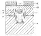
- FIGS. 5A to 5G are schematic longitudinal sectional views showing one process of the method for manufacturing the semiconductor memory device 100 according to this embodiment.
- a mask 151 for forming an opening 120A in the semiconductor substrate 110 is patterned on the semiconductor substrate 110 made of silicon.
- the mask 151 may be a single photoresist or a laminate of a hard mask such as an oxide film or a nitride film and a photoresist.
- the semiconductor substrate 110 is etched using the mask 151 to form openings 120 ⁇ / b> A corresponding to the pattern of the mask 151 in the semiconductor substrate 110.
- a first conductivity type (for example, p-type) channel implant for adjusting the threshold voltage of the field effect transistor may be formed on the semiconductor substrate 110 after the opening 120A is formed by ion implantation. .
- a gate insulating film 121, a lower electrode 120, a ferroelectric film 131, and an upper electrode 130 are sequentially formed on the semiconductor substrate 110.
- the gate insulating film 121, the lower electrode 120, the ferroelectric film 131, and the upper electrode 130 are sequentially formed on the semiconductor substrate 110 along the outer shape of the semiconductor substrate 110 provided with the opening 120A.
- the opening 120A provided in the semiconductor substrate 110 is embedded.
- the film thicknesses of the gate insulating film 121, the lower electrode 120, the ferroelectric film 131, and the upper electrode 130 can be appropriately adjusted so as to be in the above-described range in which the characteristics of the semiconductor memory device 100 are good.
- the materials constituting the gate insulating film 121, the lower electrode 120, the ferroelectric film 131, and the upper electrode 130 the materials described above can be used as appropriate.
- the surface of the semiconductor substrate 110 where the opening 120A is formed is polished by CMP (Chemical Mechanical Polishing) or the like until the surface of the semiconductor substrate 110 is exposed. Note that polishing by CMP or the like may be continued even after the surface of the semiconductor substrate 110 is exposed. 5D, the height of the surface of the semiconductor substrate 110 after polishing matches the height of the surfaces of the gate insulating film 121, the lower electrode 120, the ferroelectric film 131, and the upper electrode 130. The central portion of the upper electrode 130 may be recessed.
- CMP Chemical Mechanical Polishing
- a source or drain region 111 is formed by introducing a second conductivity type impurity (for example, n-type impurity) into the semiconductor substrate 110 on both sides of the opening 120A by ion implantation.
- a second conductivity type impurity for example, n-type impurity
- the introduction of the second conductivity type impurity into the semiconductor substrate 110 may be performed through a resist mask or the like, or may be performed without using a resist mask or the like.
- the step of forming the source or drain region 111 may be performed before or immediately after the formation of the opening 120 ⁇ / b> A in the semiconductor substrate 110.
- a mask 152 is provided on the conductive electrode layer 140A.
- the material which comprises the conductor electrode layer 140A can use the material mentioned above suitably.
- the conductive electrode layer 140A is patterned using the mask 152, thereby forming the conductive electrode 140 on the upper electrode 130 in a size that does not contact the lower electrode 120.
- the semiconductor memory device 100 according to this embodiment can be manufactured.
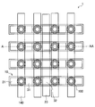
- FIG. 6 is a plan view schematically showing a planar configuration of a semiconductor device 1 in which a plurality of semiconductor memory devices 100 according to the present embodiment are arranged in a matrix
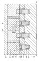
- FIG. 7 shows the semiconductor device 1 shown in FIG. It is a longitudinal cross-sectional view which shows typically the cross section cut
- the semiconductor device 1 is a storage device capable of storing a large amount of information in a plurality of semiconductor storage devices 100 arranged in a matrix.
- the semiconductor device 1 can perform a product-sum operation by using a plurality of semiconductor memory devices 100 arranged in a matrix as a synapse and using the resistance value of the channel of the semiconductor memory device 100 as a synaptic weight. It can also be used as a simple product-sum operation apparatus.
- the wiring 21 extending in the first direction (for example, the right and left direction as opposed to FIG. 6) is electrically connected to one of the source or drain region 111 of the semiconductor memory device 100 via the contact 31. ing.
- the conductor electrode 140 is provided so as to extend in a second direction (for example, up and down with respect to FIG. 6) orthogonal to the first direction.
- the wiring 23 is electrically connected to the other of the source or drain region 111 of the semiconductor memory device 100 through the contact 32.
- the semiconductor memory device 100 is provided on the semiconductor substrate 110 at each intersection of the wiring 21 orthogonal to each other and the conductor electrode 140.
- the semiconductor memory devices 100 adjacent in the second direction are electrically insulated from each other by the insulating element isolation layer 10.
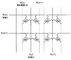
- FIG. 8 is an equivalent circuit diagram of the semiconductor device 1 shown in FIGS.
- the semiconductor device 1 when writing information, for example, the semiconductor device 1 provides a potential difference between the predetermined wiring 21 and the predetermined conductor electrode 140 so that the predetermined wiring 21 and the predetermined conductor electrode 140 A potential difference is selectively applied to the semiconductor memory device 100 existing at the intersection of the two. As a result, the semiconductor device 1 can selectively invert the residual polarization of the ferroelectric film 131 of the semiconductor memory device 100 present at the intersection of the wiring 21 and the conductor electrode 140, and can write information into the semiconductor memory device 100. .
- the semiconductor device 1 when reading information, applies a voltage to the conductor electrode 140 to turn on the field effect transistor of the semiconductor memory device 100, and then the current flowing between the wiring 21 and the wiring 23 (that is, , The current flowing between the source and drain of the semiconductor memory device 100) is measured. As a result, the semiconductor device 1 can obtain a current value corresponding to the direction of remanent polarization of the ferroelectric film 131 from each of the semiconductor memory devices 100, so that information can be read from the semiconductor memory device 100.
- FIG. 9 is a vertical cross-sectional view schematically showing a cross-sectional structure according to a modified example of the semiconductor device 1.
- the conductor electrode 140 may be electrically connected to the upper electrode 130 via the contact 33.
- the semiconductor memory device 100 according to the first embodiment of the present disclosure has been described in detail above.
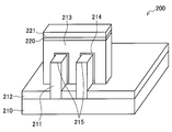
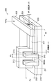
- FIG. 10 is a perspective view schematically showing a structural example of the semiconductor memory device according to the present embodiment.
- the semiconductor memory device 200 includes a semiconductor substrate 210, an insulating layer 212, a semiconductor layer 211, a source or drain region 215, a gate insulating film 214, a gate electrode 213, and a lower electrode 217.
- the semiconductor memory device 200 is an FeRAM having an MFMIS structure in which a ferroelectric capacitor is connected in series to a gate electrode of a field effect transistor.
- the field effect transistor is a Fin-type field effect transistor formed by the semiconductor layer 211, the source or drain region 215, the gate insulating film 214, and the gate electrode 213.
- the ferroelectric capacitor is formed by the lower electrode 217, the ferroelectric film 220 and the upper electrode 221.
- the ferroelectric capacitor is connected in series with the gate of the field effect transistor by electrically connecting the lower electrode 120 to the gate electrode 213 of the field effect transistor.
- the semiconductor substrate 210 is a substrate made of a semiconductor material.
- the semiconductor substrate 210 may be a silicon substrate or an SOI (Silicon On Insulator) substrate in which an insulating film such as SiO 2 is sandwiched between silicon substrates.
- the semiconductor substrate 210 is a substrate formed of another elemental semiconductor such as germanium, or a substrate formed of a compound semiconductor such as gallium arsenide (GaAs), gallium nitride (GaN), or silicon carbide (SiC). Also good.
- the semiconductor substrate 210 may be a substrate in which a semiconductor layer is stacked on a substrate made of quartz, sapphire, resin, metal, or the like.
- the insulating layer 212 is made of an insulating material and is provided on the semiconductor substrate 210.
- the insulating layer 212 electrically insulates the semiconductor substrate 210 from each component such as the gate electrode 213 and the lower electrode 217 provided on the semiconductor substrate 210.
- the insulating layer 212 electrically insulates each of the semiconductor layers 211 provided on the semiconductor substrate 210 so as to protrude.
- the insulating layer 212 may be formed of an insulating oxynitride such as silicon oxide (SiO x ), silicon nitride (SiN x ), or silicon oxynitride (SiON), for example.
- the semiconductor layer 211 is made of a semiconductor material, and is provided on the semiconductor substrate 210 so as to protrude through the insulating layer 212.
- the semiconductor layer 211 may be provided on the semiconductor substrate 210 in a convex shape in a rectangular parallelepiped shape extending in one direction.
- the semiconductor layer 211 has a flat plate shape, and may be provided on the semiconductor substrate 210 so as to be convex so that the main surface of the flat plate shape (the surface having the largest area) is perpendicular to the semiconductor substrate 210. Good.
- each of the plurality of semiconductor layers 211 may be provided on the semiconductor substrate 210 so as to protrude in parallel with each other.
- the semiconductor layer 211 may be formed of, for example, silicon or other elemental semiconductor such as germanium, and a compound semiconductor such as gallium arsenide (GaAs), gallium nitride (GaN), or silicon carbide (SiC). May be formed.
- a compound semiconductor such as gallium arsenide (GaAs), gallium nitride (GaN), or silicon carbide (SiC). May be formed.
- the gate insulating film 214 is made of an insulating material and is provided so as to cover the upper surface and side surfaces of the semiconductor layer 211 in a direction orthogonal to the extending direction of the semiconductor layer 211.
- the gate insulating film 214 may be provided so as to be sandwiched between the gate electrode 213 straddling the semiconductor layer 211 and the semiconductor layer 211 in a direction orthogonal to the extending direction of the semiconductor layer 211.
- the gate insulating film 214 may be formed of a known insulating material as a gate insulating film of a field effect transistor.
- the gate insulating film 214 may be formed of an insulating oxynitride such as silicon oxide (SiO x ), silicon nitride (SiN x ), or silicon oxynitride (SiON).
- an insulating oxynitride such as silicon oxide (SiO x ), silicon nitride (SiN x ), or silicon oxynitride (SiON).
- the gate electrode 213 is made of a conductive material, and is provided so as to straddle the semiconductor layer 211 via the gate insulating film 214 in a direction orthogonal to the extending direction of the semiconductor layer 211.
- the gate electrode 213 may be provided on the semiconductor layer 211 so as to extend in a direction orthogonal to the extending direction of the semiconductor layer 211 and intersect the semiconductor layer 211.
- the gate electrode 213 is provided to extend in a direction orthogonal to the extending direction of the semiconductor layer 211 on the plurality of semiconductor layers 211 provided to extend in parallel to each other.
- the semiconductor layer 211 may be continuously straddled on the plurality of semiconductor layers 211.
- the gate electrode 213 may be formed of polysilicon or the like, or may be formed of a metal, an alloy, or a metal compound.
- the gate insulating film 214 and the gate electrode 213 are provided at substantially the center of the semiconductor layer 211 so that the semiconductor layer 211 protrudes from both sides of the gate electrode 213. According to this, a source or drain region 215 described later can be formed in the semiconductor layer 211 protruding on both sides of the gate electrode 213.
- the source or drain region 215 is a second conductivity type (for example, n-type) region formed in the semiconductor layer 211. Specifically, the source or drain region 215 is provided in a region of the semiconductor layer 211 that protrudes on both sides of the gate electrode 213. For example, the source or drain region 215 can be provided by introducing a second conductivity type impurity (for example, an n-type impurity such as phosphorus or arsenic) into a region of the semiconductor layer 211 protruding from both sides of the gate electrode 213.
- a second conductivity type impurity for example, an n-type impurity such as phosphorus or arsenic
- any of the source or drain regions 215 provided in the semiconductor layer 211 may function as a source region, and any of them may function as a drain region. These can be arbitrarily changed by the wiring connected to each of the source or drain region 215.
- the lower electrode 217 is made of a conductive material, and is provided on the insulating layer 212 in electrical connection with the gate electrode 213. Specifically, the lower electrode 217 may be provided so as to be electrically connected to the gate electrode 213 and extend in a direction orthogonal to the extending direction of the semiconductor layer 211.
- the lower electrode 217 may be formed of polysilicon or the like, and may be formed of a metal, an alloy, or a metal compound. Note that there is no particular limitation on the location where the lower electrode 217 is formed as long as the lower electrode 217 is electrically connected to the gate electrode 213 and has an independent potential (a so-called floating state).
- the ferroelectric film 220 is made of a ferroelectric material and is provided on the lower electrode 217. Specifically, the ferroelectric film 220 is provided on the lower electrode 217 extending on the insulating layer 212.
- the ferroelectric film 220 is formed of a ferroelectric material that spontaneously polarizes and whose remanent polarization direction can be controlled by an external electric field.
- the ferroelectric film 220 is formed of a ferroelectric material containing hafnium (Hf), zirconium (Zr), silicon (Si), or oxygen (O).
- the ferroelectric film 220 is a ferroelectric material having a perovskite structure such as lead zirconate titanate (Pb (Zr, Ti) O 3 : PZT) or strontium bistrontate tantalate (SrBi 2 Ta 2 O 9 : SBT). It may be made of a material.
- the ferroelectric film 220 may be a ferroelectric film obtained by altering a film made of a high dielectric material such as HfO x , ZrO x or HfZrO x by heat treatment or the like. It may be a ferroelectric film modified by introducing atoms such as lanthanum (La), silicon (Si), or gadolinium (Gd) into the resulting film. Further, the ferroelectric film 220 may be formed of a single layer or a plurality of layers. For example, the ferroelectric film 220 may be a single layer film made of a ferroelectric material such as HfO x .
- the upper electrode 221 is made of a conductive material and is provided on the ferroelectric film 220.
- the upper electrode 221 may be formed of a metal such as titanium (Ti) or tungsten (W), or a metal compound such as titanium nitride (TiN) or tantalum nitride (TaN).
- the conductor electrode 222 is made of a conductive material and is provided on the upper electrode 221.
- the conductor electrode 222 may be provided on the upper electrode 221 by extending in the extending direction of the semiconductor layer 211. That is, the conductor electrode 222 and the lower electrode 217 are provided so as to be orthogonal to each other, and the ferroelectric film 220 and the upper electrode 221 are connected to the conductor electrode 222 and the lower electrode 217 at the intersection of the conductor electrode 222 and the lower electrode 217. You may provide so that it may be clamped.
- the conductor electrode 222 may be formed of a metal material such as copper (Cu) or aluminum (Al).
- FIGS. 11A to 11D are longitudinal sectional views schematically showing structures according to modifications of the semiconductor memory device 200.
- FIG. 11A to 11D are longitudinal sectional views schematically showing structures according to modifications of the semiconductor memory device 200.
- a plurality of semiconductor layers 211 may be provided.
- the upper limit of the number of semiconductor layers 211 is not particularly limited.
- each of the plurality of semiconductor layers 211 may be provided on the semiconductor substrate 210 in a convex manner so that the extending directions are parallel to each other.
- the gate electrode 213 extends over the plurality of semiconductor layers 211 provided in parallel with each other so as to extend in a direction perpendicular to the extending direction of the semiconductor layer 211, so that the top of the plurality of semiconductor layers 211 is formed. It may be straddled continuously.
- the gate insulating film 214 may be provided so as to be sandwiched between the semiconductor layer 211 and the gate electrode 213.
- the upper electrode 221 may be provided in a wiring shape extending in the extending direction of the semiconductor layer 211, similarly to the conductor electrode 222.
- the upper electrode 221 may be formed in the same shape as the conductor electrode 222, and a wiring may be formed by the conductor electrode 222 and the upper electrode 221.
- the ferroelectric film 220 and the upper electrode 221 may be sequentially stacked on the gate electrode 216.
- the area where the ferroelectric film 220 and the upper electrode 221 are stacked may be the entire upper surface of the gate electrode 216 as shown in FIG. 11C or a part of the upper surface of the gate electrode 216 as shown in FIG. 11D. May be.
- a conductor electrode 222 (not shown) may be stacked on the upper electrode 221. In such a case, the semiconductor memory device 200 can further reduce the planar area of the unit cell.
- the lower electrode 217 may be omitted.
- the field effect transistor is provided as a so-called Fin-type transistor.
- a channel is three-dimensionally formed across a plurality of side surfaces and the upper surface of the semiconductor layer 211.
- the field effect transistor is compared with a planar field effect transistor (a field effect transistor in which a gate insulating film and a gate electrode are stacked in parallel on a semiconductor substrate) formed on a semiconductor substrate of the same area. Since the channel area can be further increased, the gate capacitance Ci can be increased.
- the gate capacitance Ci of the field effect transistor is increased without increasing the size of the unit cell, and the distribution voltage applied to the ferroelectric film 220 is further increased. be able to. Accordingly, since the semiconductor memory device 200 can apply a sufficient voltage to the ferroelectric film 220, the stability of information writing and erasing operations can be improved.
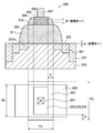
- FIG. 12 is a perspective view defining dimensions of each component of the semiconductor memory device 200 shown in FIG.
- the width in the direction orthogonal to the extending direction of the semiconductor layer 211 is px
- the height of the semiconductor layer 211 from the surface of the insulating layer 212 is py
- the number of the semiconductor layers 211 is N.
- the width of the conductor electrode 222 in the direction orthogonal to the extending direction of the semiconductor layer 211 is qx
- the width of the gate electrode 213 and the lower electrode 217 in the extending direction of the semiconductor layer 211 is the same.
- the film thickness of the gate insulating film 214 is di
- the film thickness of the ferroelectric film 220 is df
- the relative dielectric constant of the gate insulating film 214 is ⁇ i
- the relative dielectric constant of the ferroelectric film 220 is ⁇ f. In such a case, it is possible to improve the characteristics of the semiconductor memory device 200 by controlling the dimensions of the components so as to satisfy the conditions described below.
- the characteristics of the semiconductor memory device 200 can be improved by appropriately designing px, py, N, qx, df, and di so that the above-described Ef and Ei satisfy the preferable ranges.
- FIG. 13 is a plan view schematically showing a planar configuration of a semiconductor device 2 in which a plurality of semiconductor memory devices 200 according to the present embodiment are arranged in a matrix.
- the semiconductor device 2 is a storage device capable of storing a large amount of information in a plurality of semiconductor storage devices 200 arranged in a matrix. Further, the semiconductor device 2 can perform a product-sum operation by using a plurality of semiconductor memory devices 200 arranged in a matrix as a synapse and using the resistance value of the channel of the semiconductor memory device 200 as a synapse weight. It can also be used as a simple product-sum operation apparatus.
- the wiring 251 extending in the first direction (for example, the right and left direction as opposed to FIG. 13) is electrically connected to one of the source or drain region 215 of the semiconductor memory device 200 via the contact 255.
- a wiring 252 extending in a second direction orthogonal to the first direction (for example, up and down with respect to FIG. 13) is electrically connected to the other of the source or drain region 111 of the semiconductor memory device 200 through a contact 256.
- the conductor electrode 222 is provided to extend in a second direction (for example, up and down with respect to FIG. 13) orthogonal to the first direction.
- a ferroelectric capacitor is provided at the intersection of the conductor electrode 222 orthogonal to each other and the gate electrode 213 and the lower electrode 217.
- the semiconductor device 2 When writing information, the semiconductor device 2 is provided at the intersection of the conductor electrode 222, the gate electrode 213, and the lower electrode 217, for example, by providing a potential difference between the predetermined wiring 251 and the predetermined conductor electrode 222. A potential difference is selectively applied to the ferroelectric capacitor. Thereby, the semiconductor device 2 can selectively invert the remanent polarization of the ferroelectric film 220 of the predetermined ferroelectric capacitor and write information in the semiconductor memory device 200.
- the semiconductor device 2 when reading information, for example, the semiconductor device 2 applies a voltage to the conductor electrode 222 to turn on the field effect transistor of the semiconductor memory device 200, and then the current flowing between the wiring 251 and the wiring 252 (that is, , The current flowing between the source and the drain of the semiconductor memory device 200 is measured. As a result, the semiconductor device 2 can obtain a current value corresponding to the direction of remanent polarization of the ferroelectric film 220 from each of the semiconductor memory devices 200, so that information can be read from the semiconductor memory device 200.
- the semiconductor memory device 200 according to the second embodiment of the present disclosure has been described in detail above.
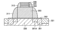
- FIG. 14 is a longitudinal sectional view schematically showing a structural example of the semiconductor memory device according to the present embodiment.
- the semiconductor memory device 300 includes a semiconductor substrate 320, an element isolation layer 321, a source or drain region 301, an LDD region 301A, a gate insulating film 302, a gate electrode 303, a first side.
- a wall 311, a lower electrode 304, a ferroelectric film 305, an upper electrode 306, a second sidewall 312, and a conductor electrode 307 are provided.
- the semiconductor memory device 300 is an FeRAM having an MFMIS structure in which a ferroelectric capacitor is connected in series on a gate electrode of a field effect transistor.
- the field effect transistor is formed by the semiconductor substrate 320, the source or drain region 301, the LDD region 301A, the gate insulating film 302, and the gate electrode 303, and the ferroelectric capacitor is formed by the lower electrode 304, the ferroelectric film. 305 and the upper electrode 306 are formed.
- the ferroelectric capacitor is connected in series with the gate of the field effect transistor at the lower electrode 304.
- the semiconductor substrate 320 is a substrate made of a semiconductor material.
- a first conductivity type impurity (for example, a p-type impurity such as boron or aluminum) is introduced into the semiconductor substrate 320 in a region where the semiconductor memory device 300 is formed.
- the semiconductor substrate 320 may be a silicon substrate or an SOI (Silicon On Insulator) substrate in which an insulating film such as SiO 2 is sandwiched between silicon substrates.
- the semiconductor substrate 320 is a substrate formed of another elemental semiconductor such as germanium, or a substrate formed of a compound semiconductor such as gallium arsenide (GaAs), gallium nitride (GaN), or silicon carbide (SiC). Also good.
- the semiconductor substrate 320 may be a substrate in which a semiconductor layer is stacked on a substrate made of quartz, sapphire, resin, metal, or the like.
- the element isolation layer 321 is made of an insulating material and electrically insulates the semiconductor memory devices 300 provided on the semiconductor substrate 320 from each other.
- the element isolation layer 321 may be formed of an insulating oxynitride such as silicon oxide (SiO x ), silicon nitride (SiN x ), or silicon oxynitride (SiON).
- the element isolation layer 321 is formed by removing a part of the semiconductor substrate 320 in a predetermined region by etching or the like using an STI (Shallow Trench Isolation) method, and then opening an opening formed by etching or the like with silicon oxide ( It may be formed by embedding with SiO x ).
- the element isolation layer 321 may be formed by thermally oxidizing the semiconductor substrate 320 in a predetermined region using a LOCOS (Local Oxidation of Silicon) method.
- the source or drain region 301 is a second conductivity type (for example, n-type) region formed in the semiconductor substrate 320. Specifically, the source or drain region 301 is provided by introducing a second conductivity type impurity (for example, an n-type impurity such as phosphorus or arsenic) into the semiconductor substrate 320 on both sides with the gate electrode 213 interposed therebetween. .
- a second conductivity type impurity for example, an n-type impurity such as phosphorus or arsenic
- the semiconductor substrate 320 between the source or drain region 301 and the gate electrode 303 has the same second conductivity type (for example, n-type) as the source or drain region 301 and more than the source or drain region 301.
- An LDD (Lightly-Doped Drain) region 301A having a low concentration of conductive impurities may be formed.
- any of the source or drain regions 301 provided on both sides of the gate electrode 303 may function as a source region, and any of them may function as a drain region. These can be arbitrarily changed by the wiring connected to each of the source or drain regions 301.
- the gate insulating film 302 is made of an insulating material and is provided on the semiconductor substrate 320.
- the gate insulating film 302 may be formed of a known insulating material as a gate insulating film of a field effect transistor.
- the gate insulating film 302 may be formed of an insulating oxynitride such as silicon oxide (SiO x ), silicon nitride (SiN x ), or silicon oxynitride (SiON).
- the gate electrode 303 is made of a conductive material and is provided on the gate insulating film 302.
- the gate electrode 303 may be provided on the semiconductor layer 211 so as to extend in a direction orthogonal to the extending direction of the semiconductor layer 211 and intersect the semiconductor layer 211.
- the gate electrode 303 may be formed of polysilicon or the like, or may be formed of a metal, an alloy, or a metal compound.
- the first sidewall 311 is made of an insulating material and is provided as a sidewall on the side surface of the gate electrode 303.
- the first sidewall 311 can be formed by forming an insulating film uniformly in a region including the gate electrode 303 and then performing vertical anisotropic etching on the insulating film.
- the first sidewall 311 may be formed of a single layer or a plurality of layers of an insulating oxynitride such as silicon oxide (SiO x ), silicon nitride (SiN x ), or silicon oxynitride (SiON). Good.
- the first sidewall 311 self-aligns the positional relationship between the gate electrode 303 and the source or drain region 301 by shielding the second conductivity type impurity when introducing the second conductivity type impurity into the semiconductor substrate 320. Control.
- the introduction of the second conductivity type impurity into the semiconductor substrate 320 can be controlled in stages, so that the LDD region 301 ⁇ / b> A is provided between the source or drain region 301 and the gate electrode 303. Can be formed in a self-aligned manner.
- the lower electrode 304 is made of a conductive material and is provided on the gate electrode 303.
- the lower electrode 304 may be formed of polysilicon or the like, and may be formed of a metal, an alloy, or a metal compound.
- the ferroelectric film 305 is made of a ferroelectric material and is provided on the lower electrode 304.
- the ferroelectric film 305 is made of a ferroelectric material that spontaneously polarizes and whose direction of remanent polarization can be controlled by an external electric field.
- the ferroelectric film 305 is formed of a ferroelectric material containing hafnium (Hf), zirconium (Zr), silicon (Si), or oxygen (O).
- the ferroelectric film 305 is a ferroelectric material having a perovskite structure such as lead zirconate titanate (Pb (Zr, Ti) O 3 : PZT) or strontium bistrontate tantalate (SrBi 2 Ta 2 O 9 : SBT). It may be made of a material.
- the ferroelectric film 305 may be a ferroelectric film obtained by modifying a film made of a high dielectric material such as HfO x , ZrO x or HfZrO x by heat treatment or the like. It may be a ferroelectric film modified by introducing atoms such as lanthanum (La), silicon (Si), or gadolinium (Gd) into the resulting film.
- the ferroelectric film 305 may be formed of a single layer or a plurality of layers.
- the ferroelectric film 305 may be a single layer film made of a ferroelectric material such as HfO x .
- the upper electrode 306 is made of a conductive material and is provided on the ferroelectric film 305.
- the upper electrode 306 may be formed of a metal such as titanium (Ti) or tungsten (W), or a metal compound such as titanium nitride (TiN) or tantalum nitride (TaN).
- the lower electrode 304, the ferroelectric film 305, and the upper electrode 306 are provided in the same plane shape, and the second electrode 304, the ferroelectric film 305, and the upper electrode 306 are formed on the side surface of the stacked body. Sidewalls 312 are provided.
- the second side wall 312 is made of an insulating material and is provided as a side wall on the side surface of the stacked body of the lower electrode 304, the ferroelectric film 305 and the upper electrode 306. Specifically, the second sidewall 312 is formed by uniformly forming an insulating film on the stacked body of the lower electrode 304, the ferroelectric film 305, and the upper electrode 306, and then forming the insulating film with the vertical anisotropy. It can be formed by etching.
- the second sidewall 312 may be formed of a single layer or a plurality of layers of an insulating oxynitride such as silicon oxide (SiO x ), silicon nitride (SiN x ), or silicon oxynitride (SiON). Good.
- an insulating oxynitride such as silicon oxide (SiO x ), silicon nitride (SiN x ), or silicon oxynitride (SiON). Good.
- the planar area occupied by the stacked body of the lower electrode 304, the ferroelectric film 305 and the upper electrode 306 and the second sidewall 312 can be substantially equal to the planar area of the upper surface of the gate electrode 303.
- a stacked body of the lower electrode 304, the ferroelectric film 305 and the upper electrode 306 and the second sidewall 312 are formed by etching, and then the stacked body and the second side are formed.
- the gate electrode 303 is formed.
- the stacked body of the lower electrode 304, the ferroelectric film 305 and the upper electrode 306, the second sidewall 312, the gate electrode 303, and the first sidewall 311 are formed in a self-aligned manner. can do.
- the conductor electrode 307 is made of a conductive material and is provided on the upper electrode 306.
- the conductor electrode 307 functions as a connection terminal of the semiconductor memory device 300 by being electrically connected to another wiring (not shown).
- the conductor electrode 307 may be formed of a metal material such as titanium (Ti), tungsten (W), copper (Cu), or aluminum (Al).
- the field effect transistor is provided as a so-called planar transistor, and the ferroelectric capacitor is provided together with the second sidewall 312 on the gate electrode of the field effect transistor.
- the area of the ferroelectric film 305 of the ferroelectric capacitor is smaller by one than the area of the gate insulating film 302 of the field effect transistor by the width of the second sidewall 312.
- the gate capacitance Ci of the field effect transistor can be made larger than the capacitance Cf of the ferroelectric capacitor.
- the gate capacitance Ci of the field effect transistor is increased without increasing the size of the unit cell, and the distribution voltage applied to the ferroelectric film 305 is further increased. be able to. Accordingly, since the semiconductor memory device 300 can apply a sufficient voltage to the ferroelectric film 305, the stability of information writing and erasing operations can be improved.
- FIG. 15 is a longitudinal sectional view defining dimensions of each component of the semiconductor memory device 300 shown in FIG.
- the width of the gate electrode 303 in the direction in which the source or drain region 301 is provided (also referred to as the channel direction) is Px, and the length of the gate electrode 303 in the direction orthogonal to the channel direction is Py.
- the length of the source or drain region 301 in the direction orthogonal to the channel direction is Qy, and the width of the second sidewall 312 is X.
- the film thickness of the gate insulating film 302 is di
- the film thickness of the ferroelectric film 305 is df
- the relative dielectric constant of the gate insulating film 302 is ⁇ i
- the relative dielectric constant of the ferroelectric film 305 is ⁇ f.
- the characteristics of the semiconductor memory device 300 can be improved by appropriately designing Px, Py, Qy, X, df, and di so that the above-described Ef and Ei satisfy a preferable range.
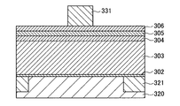
- FIGS. 16A to 16E are schematic longitudinal sectional views showing one process of the method for manufacturing the semiconductor memory device 300 according to this embodiment.
- a gate insulating film 302, a gate electrode 303, a lower electrode 304, a ferroelectric film 305, and an upper electrode 306 are uniformly formed on a semiconductor substrate 320 on which an element isolation layer 321 is formed. Form a film. Further, a mask 331 for forming a ferroelectric capacitor is patterned on the upper electrode 306.
- the mask 331 may be a single photoresist or a laminate of a hard mask such as an oxide film or a nitride film and a photoresist.
- the lower electrode 304, the ferroelectric film 305, and the upper electrode 306 are simultaneously etched using a mask 331, so that a ferroelectric capacitor having a size corresponding to the pattern of the mask 331 ( That is, a laminate of a lower electrode 304, a ferroelectric film 305, and an upper electrode 306) is formed.
- an insulating film is uniformly formed on the stacked body of the lower electrode 304, the ferroelectric film 305, and the upper electrode 306, and then the entire surface is etched back, whereby the second side A wall 312 is formed.
- the gate electrode 303 is etched using the stacked body of the lower electrode 304, the ferroelectric film 305 and the upper electrode 306, and the second sidewall 312 as a mask. According to this, since it is possible to omit providing a mask for patterning the gate electrode 303, the manufacturing cost of the semiconductor memory device 300 can be reduced.
- a source or drain region 301 is formed by introducing a second conductivity type impurity (for example, n-type impurity) into the semiconductor substrate 320 by ion implantation.
- a second conductivity type impurity for example, n-type impurity
- the LDD region 301A may be formed in a self-aligned manner between the gate electrode 303 and the source or drain region 301 by forming the first sidewall 311.
- the semiconductor memory device 300 according to this embodiment can be manufactured.
- FIGS. 17 to 19 are longitudinal sectional views schematically showing structures according to modifications of the semiconductor memory device 300.
- FIG. 17 to 19 are longitudinal sectional views schematically showing structures according to modifications of the semiconductor memory device 300.
- the ferroelectric capacitor composed of the lower electrode 304, the ferroelectric film 305, and the upper electrode 306 is connected in series with the gate electrode 303 of the field effect transistor through the conductor electrode 323. May be.
- the conductor electrode 323 may be formed of a metal material such as titanium (Ti), tungsten (W), copper (Cu), or aluminum (Al) as in the case of the conductor electrode 307 described above.
- the characteristics of the semiconductor memory device 300 can be improved by controlling the dimensions of the respective components so as to satisfy the conditions described below.
- the width of the gate electrode 303 in the direction in which the source or drain region 301 is provided (also referred to as the channel direction) is Px, and the length of the source or drain region 301 is Py.
- the width of the ferroelectric capacitor in the channel direction (that is, the stacked body of the lower electrode 304, the ferroelectric film 305, and the upper electrode 306) is Qx, and the length of the ferroelectric capacitor in the direction orthogonal to the channel direction is Qy. To do.
- the film thickness of the gate insulating film 302 is di
- the film thickness of the ferroelectric film 305 is df
- the relative dielectric constant of the gate insulating film 302 is ⁇ i
- the relative dielectric constant of the ferroelectric film 305 is ⁇ f. .
- the characteristics of the semiconductor memory device 300 can be improved by appropriately designing Px, Py, Qy, Qx, df, and di so that the above-described Ef and Ei satisfy a preferable range.
- the ferroelectric capacitor is not a stacked body of the lower electrode 304, the ferroelectric film 305, and the upper electrode 306, but is formed on the lower electrode 304 by using the damascene process. It may have a structure in which the electrode 306 is embedded.
- the structure of the semiconductor memory device 300 shown in FIG. 18 is different from the structure of the semiconductor memory device 300 shown in FIG.
- the width of the gate electrode 303 in the direction in which the source or drain region 301 is provided (also referred to as the channel direction) is Px, and the length of the source or drain region 301 is Py.
- the width of the ferroelectric capacitor in the channel direction is Qx, and the length of the ferroelectric capacitor in the direction orthogonal to the channel direction is Qy.
- the film thickness of the gate insulating film 302 is di
- the film thickness of the ferroelectric film 305 is df
- the relative dielectric constant of the gate insulating film 302 is ⁇ i
- the relative dielectric constant of the ferroelectric film 305 is ⁇ f.
- the height of the lower electrode 304 (that is, the height of the ferroelectric capacitor) is hf
- the thickness of the lower electrode 304 is Tf.
- Ef Vprg / df ⁇ (1+ ( ⁇ f ⁇ di) / ( ⁇ i ⁇ df) ⁇ Sf / Si)
- Ei di ⁇ (Vprg ⁇ Vf)
- Sf 2 (hf-Tf-df).
- Qy-2df-2hf) Si Px ⁇ Py It is.
- the characteristics of the semiconductor memory device 300 can be improved by appropriately designing Px, Py, Qy, Qx, Tf, hf, df, and di so that Ef and Ei described above satisfy a preferable range. It is.
- the lower electrode 304 may be omitted.
- the semiconductor memory device 300 shown in FIG. 19 is different from the semiconductor memory device 300 shown in FIG. 18 in that a ferroelectric capacitor includes a conductor electrode 323, a ferroelectric film 305, and an upper electrode 306. Is different.
- the characteristics of the semiconductor memory device 300 can be improved by controlling the dimensions of the respective components so as to satisfy the conditions described below.
- the width of the gate electrode 303 in the direction in which the source or drain region 301 is provided (also referred to as the channel direction) is Px, and the length of the source or drain region 301 is Py.
- the width of the ferroelectric capacitor in the channel direction is Qx, and the length of the ferroelectric capacitor in the direction orthogonal to the channel direction is Qy.
- the film thickness of the gate insulating film 302 is di
- the film thickness of the ferroelectric film 305 is df
- the relative dielectric constant of the gate insulating film 302 is ⁇ i
- the relative dielectric constant of the ferroelectric film 305 is ⁇ f.
- the height of the ferroelectric film 305 (that is, the height of the ferroelectric capacitor) is hf
- the width of the conductor electrode 323 is Cx.
- the characteristics of the semiconductor memory device 300 can be improved by appropriately designing Px, Py, Qy, Qx, hf, Cx, df, and di so that the above-described Ef and Ei satisfy a preferable range. It is.
- the planar shape of the conductor electrode 323 is substantially square, but the planar shape of the conductor electrode 323 may be any of a rectangle, a circle, and an ellipse.
- the semiconductor memory device 300 according to the third embodiment of the present disclosure has been described above in detail.
- the semiconductor storage device 300 according to the third embodiment of the present disclosure is applied to a storage device capable of storing a large amount of information by being arranged in a matrix like the semiconductor storage devices 100 and 200. Is possible. Further, the semiconductor memory device 300 can also be applied to a product-sum operation apparatus that can perform a product-sum operation by being used as a synapse.
- a transistor A ferroelectric capacitor formed by sandwiching a ferroelectric material between a pair of conductive materials, wherein one of the conductive materials is electrically connected to the gate electrode of the transistor; With The semiconductor memory device, wherein the channel of the transistor is three-dimensionally formed over a plurality of surfaces.
- the semiconductor memory device according to (1) wherein an electric field applied to the ferroelectric material of the ferroelectric capacitor is greater than 2 MV / cm.
- the transistor is provided on the gate insulating film so as to embed the semiconductor substrate, a gate insulating film provided along an internal shape of the opening formed in the semiconductor substrate, and the opening of the semiconductor substrate.
- a gate electrode, The ferroelectric capacitor is provided on the gate electrode so as to embed the ferroelectric film provided along the internal shape of the opening formed in the gate electrode and the opening of the gate electrode.
- the semiconductor memory device according to any one of (1) to (3), comprising an upper electrode.
- the semiconductor substrate is of a first conductivity type;
- the semiconductor memory device according to (4), wherein a source or drain region of a second conductivity type different from the first conductivity type is provided on a surface side of the semiconductor substrate where the opening is provided.
- the semiconductor memory device wherein the opening of the semiconductor substrate is provided to a region deeper than the source or drain region.
- the transistor covers a semiconductor layer extending in one direction on a substrate, and covers an upper surface and side surfaces of the semiconductor layer in a direction orthogonal to the extending direction of the semiconductor layer.
- the ferroelectric capacitor includes one of the conductive materials stacked on the gate electrode, the ferroelectric material stacked on one of the conductive materials, and a stack on the ferroelectric material.
- the semiconductor memory device according to (7), further including the other of the conductive materials formed.
- a plurality of the semiconductor layers are provided to be parallel to each other, The semiconductor memory device according to (8), wherein the gate electrode is provided continuously over the plurality of semiconductor layers.
- the ferroelectric capacitor includes the contact electrode or one of the conductive materials laminated on the contact electrode, the ferroelectric material laminated on one of the conductive materials,
- a transistor A ferroelectric capacitor formed by sandwiching a ferroelectric material between a pair of conductive materials, wherein one of the conductive materials is electrically connected to the gate electrode of the transistor; With The pair of conductive materials and the ferroelectric material are stacked in parallel with the upper surface of the gate electrode, so that the ferroelectric capacitor is provided on the gate electrode, The product-sum operation device, wherein a planar area of the ferroelectric capacitor is smaller than a planar area of the upper surface of the gate electrode.
Landscapes
- Semiconductor Memories (AREA)
- Internal Circuitry In Semiconductor Integrated Circuit Devices (AREA)
- Semiconductor Integrated Circuits (AREA)
- Metal-Oxide And Bipolar Metal-Oxide Semiconductor Integrated Circuits (AREA)
- Non-Volatile Memory (AREA)
- Insulated Gate Type Field-Effect Transistor (AREA)
Abstract
【課題】強誘電体キャパシタに十分な電圧を印加することが可能であり、かつ高集積化に適した半導体記憶装置及び積和演算装置を提供する。 【解決手段】トランジスタと、一対の導電材料で強誘電体材料を挟持することで形成され、前記導電材料の一方が前記トランジスタのゲート電極と電気的に接続された強誘電体キャパシタと、を備え、前記トランジスタのチャネルは、複数の面に亘って立体的に形成される、半導体記憶装置。
Description
本開示は、半導体記憶装置及び積和演算装置に関する。
近年、次世代メモリとして強誘電体メモリ(Ferroelectric Random Access Memory:FeRAM)が注目されている。FeRAMは、強誘電体の残留分極の方向を用いて情報を記憶する半導体記憶装置である。
FeRAMの構造の1つとして、例えば、半導体基板の上に形成されたMIS(Metal-Insulator-Semiconductor)型電界効果トランジスタのゲート電極の上に、下部電極、強誘電体膜及び上部電極を順に積層することで強誘電体キャパシタを形成する構造が知られている。このような構造は、MFMIS(Metal-Ferroelectric-Metal-Insulator-Semiconductor)構造とも称される。
MFMIS構造のFeRAMでは、半導体基板及び上部電極の間に電圧を印加するため、印加された電圧は、MIS型電界効果トランジスタのゲート絶縁膜と、強誘電体キャパシタの強誘電体膜とに分配される。そのため、MIS型電界効果トランジスタのゲート容量、及び強誘電体キャパシタの容量の比率によっては、強誘電体膜の分極を反転させるために十分な電圧を強誘電体膜に印加することができないことがあった。
例えば、下記の特許文献1には、MFMIS構造のFeRAMにおいて、一端がMIS型電界効果トランジスタのゲート電極及び強誘電体キャパシタの下部電極の間に接続され、他端がMIS型電界効果トランジスタのソースに接続された常誘電体キャパシタをさらに設けることで、強誘電体キャパシタの分配電圧を高くする技術が開示されている。
しかし、上記の特許文献1に開示される技術では、半導体基板の上に常誘電体キャパシタが形成される領域をさらに設ける必要があるため、FeRAMの単位セルあたりの面積が大きくなってしまう。そのため、特許文献1に開示されるFeRAMは、高集積化が困難であった。
そこで、本開示では、強誘電体キャパシタに十分な電圧を印加することが可能であり、かつ高集積化に適した構造を有する、新規かつ改良された半導体記憶装置及び積和演算装置を提案する。
本開示によれば、トランジスタと、一対の導電材料で強誘電体材料を挟持することで形成され、前記導電材料の一方が前記トランジスタのゲート電極と電気的に接続された強誘電体キャパシタと、を備え、前記トランジスタのチャネルは、複数の面に亘って立体的に形成される、半導体記憶装置が提供される。
また、本開示によれば、トランジスタと、一対の導電材料で強誘電体材料を挟持することで形成され、前記導電材料の一方が前記トランジスタのゲート電極と電気的に接続される強誘電体キャパシタと、を備え、前記トランジスタのチャネルは、複数の面に亘って立体的に形成される、積和演算装置が提供される。
また、本開示によれば、トランジスタと、一対の導電材料で強誘電体材料を挟持することで形成され、前記導電材料の一方が前記トランジスタのゲート電極と電気的に接続された強誘電体キャパシタと、を備え、前記一対の導電材料、及び前記強誘電体材料は、前記ゲート電極の上面と平行に積層されることで、前記強誘電体キャパシタは、前記ゲート電極の上に設けられ、前記強誘電体キャパシタの平面面積は、前記ゲート電極の上面の平面面積よりも小さい、半導体記憶装置が提供される。
さらに、本開示によれば、トランジスタと、一対の導電材料で強誘電体材料を挟持することで形成され、前記導電材料の一方が前記トランジスタのゲート電極と電気的に接続された強誘電体キャパシタと、を備え、前記一対の導電材料、及び前記強誘電体材料は、前記ゲート電極の上面と平行に積層されることで、前記強誘電体キャパシタは、前記ゲート電極の上に設けられ、前記強誘電体キャパシタの平面面積は、前記ゲート電極の上面の平面面積よりも小さい、積和演算装置が提供される。
本開示によれば、半導体記憶装置は、単位セルの大きさを増大させることなく、電界効果トランジスタのゲート容量を増大させることで、強誘電体キャパシタの強誘電体膜に印加される分配電圧をより高くすることができる。
以上説明したように本開示によれば、強誘電体キャパシタに十分な電圧を印加することが可能であり、かつ高集積化に適した構造を有する半導体記憶装置及び積和演算装置を提供することができる。
なお、上記の効果は必ずしも限定的なものではなく、上記の効果とともに、または上記の効果に代えて、本明細書に示されたいずれかの効果、または本明細書から把握され得る他の効果が奏されてもよい。
以下に添付図面を参照しながら、本開示の好適な実施の形態について詳細に説明する。なお、本明細書及び図面において、実質的に同一の機能構成を有する構成要素については、同一の符号を付することにより重複説明を省略する。
以下の説明にて参照する各図面では、説明の便宜上、一部の構成部材の大きさを誇張して表現している場合がある。したがって、各図面において図示される構成部材同士の相対的な大きさは、必ずしも実際の構成部材同士の大小関係を正確に表現するものではない。また、以下の説明では、基板又は層が積層される方向を上方向と表現することがある。
なお、説明は以下の順序で行うものとする。
1.第1の実施形態
1.1.構造例
1.2.設計例
1.3.製造方法
1.4.適用例
2.第2の実施形態
2.1.構造例
2.2.設計例
2.3.適用例
3.第3の実施形態
3.1.構造例
3.2.設計例
3.3.製造方法
3.4.変形例
1.第1の実施形態
1.1.構造例
1.2.設計例
1.3.製造方法
1.4.適用例
2.第2の実施形態
2.1.構造例
2.2.設計例
2.3.適用例
3.第3の実施形態
3.1.構造例
3.2.設計例
3.3.製造方法
3.4.変形例
<1.第1の実施形態>
(1.1.構造例)
まず、図1を参照して、本開示の第1の実施形態に係る半導体記憶装置の構造例について説明する。図1は、本実施形態に係る半導体記憶装置の構造例を模式的に示す縦断面図である。
(1.1.構造例)
まず、図1を参照して、本開示の第1の実施形態に係る半導体記憶装置の構造例について説明する。図1は、本実施形態に係る半導体記憶装置の構造例を模式的に示す縦断面図である。
図1に示すように、半導体記憶装置100は、半導体基板110と、ソース又はドレイン領域111と、ゲート絶縁膜121と、下部電極120と、強誘電体膜131と、上部電極130と、導体電極140と、を備える。
半導体記憶装置100は、電界効果トランジスタのゲート電極の上に強誘電体キャパシタを直列に接続したMFMIS構造を有するFeRAMである。具体的には、電界効果トランジスタは、半導体基板110、ソース又はドレイン領域111、ゲート絶縁膜121及び下部電極120によって形成され、強誘電体キャパシタは、下部電極120、強誘電体膜131及び上部電極130によって形成される。強誘電体キャパシタは、下部電極120にて電界効果トランジスタのゲートと直列に接続している。
半導体基板110は、半導体材料にて構成される基板である。半導体記憶装置100が形成される領域の半導体基板110には、第1導電型の不純物(例えば、ホウ素又はアルミニウムなどのp型不純物)が導入されている。半導体基板110は、シリコン基板であってもよく、シリコン基板の中にSiO2等の絶縁膜を挟み込んだSOI(Silicon On Insulator)基板であってもよい。または、半導体基板110は、ゲルマニウムなどの他の元素半導体で形成された基板、又はガリウムヒ素(GaAs)、窒化ガリウム(GaN)若しくはシリコンカーバイド(SiC)等の化合物半導体で形成された基板であってもよい。さらには、半導体基板110は、石英、サファイア、樹脂又は金属等で構成された基板上に半導体層を積層した基板であってもよい。
ソース又はドレイン領域111は、半導体基板110に形成された第2導電型(例えば、n型)の領域である。具体的には、ソース又はドレイン領域111は、半導体基板110に設けられた開口の両側の領域に第2導電型の不純物(例えば、リン又はヒ素などのn型不純物)を導入することで設けられる。半導体基板110に設けられた開口の内部には、電界効果トラジスタ及び強誘電体キャパシタが形成される。なお、ソース又はドレイン領域111は、互いに離隔されていれば、必ずしも半導体基板110に設けられた開口の両側に設けられずともよい。
なお、半導体基板110に設けられた開口の両側に形成されたソース又はドレイン領域111は、いずれがソース領域として機能してもよく、いずれがドレイン領域として機能してもよい。これらは、ソース又はドレイン領域111の各々に接続される配線によって任意に変更され得る。
ゲート絶縁膜121は、絶縁性材料で構成され、半導体基板110に形成された開口の内部形状に沿って設けられる。具体的には、半導体基板110に形成された開口は、半導体基板110のソース又はドレイン領域111よりも深い領域まで設けられ、ゲート絶縁膜121は、該開口の底面及び側面に沿って設けられる。ゲート絶縁膜121は、電界効果トランジスタのゲート絶縁膜として公知の絶縁性材料で形成されてもよい。例えば、ゲート絶縁膜121は、酸化シリコン(SiOx)、窒化シリコン(SiNx)又は酸窒化シリコン(SiON)などの絶縁性の酸窒化物で形成されてもよい。
下部電極120は、導電性材料で構成され、半導体基板110に形成された開口を埋め込むようにゲート絶縁膜121の上に設けられる。例えば、下部電極120は、ポリシリコン等にて形成されてもよく、金属、合金又は金属化合物にて形成されてもよい。なお、下部電極120は、他の配線と電気的に接続されておらず、電位が独立した状態(いわゆる、フローティング状態)として設けられる。
強誘電体膜131は、強誘電体材料にて構成され、下部電極120に設けられた開口の内部形状に沿って設けられる。具体的には、下部電極120に設けられた開口は、下部電極120の内側に設けられ、強誘電体膜131は、該開口の底面及び側面に沿って設けられる。なお、下部電極120に設けられた開口は、ゲート絶縁膜121を露出されるように設けられてもよい。
強誘電体膜131は、自発的に分極し、かつ残留分極の方向を外部電界にて制御可能な強誘電体材料にて形成される。具体的には、強誘電体膜131は、ハフニウム(Hf)、ジルコニウム(Zr)、シリコン(Si)又は酸素(O)を含む強誘電体材料で形成される。例えば、強誘電体膜131は、チタン酸ジルコン酸鉛(Pb(Zr,Ti)O3:PZT)又はタンタル酸ビスマス酸ストロンチウム(SrBi2Ta2O9:SBT)などのペレブスカイト構造の強誘電体材料にて形成されてもよい。また、強誘電体膜131は、HfOx、ZrOx又はHfZrOxなどの高誘電体材料からなる膜を熱処理等によって変質させた強誘電体膜であってもよく、上記の高誘電体材料からなる膜にランタン(La)、シリコン(Si)又はガドリニウム(Gd)などの原子を導入することで変質させた強誘電体膜であってもよい。さらに、強誘電体膜131は、単層にて形成されてもよく、複数層にて形成されてもよい。例えば、強誘電体膜131は、HfOxなどの強誘電体材料からなる単層膜であってもよい。
上部電極130は、導電性材料で構成され、下部電極120に形成された開口を埋め込むように強誘電体膜131の上に設けられる。例えば、上部電極130は、チタン(Ti)若しくはタングステン(W)などの金属、又は窒化チタン(TiN)若しくは窒化タンタル(TaN)などの金属化合物で形成されてもよい。
導体電極140は、導電性材料で構成され、上部電極130の上に設けられる。ただし、導体電極140は、下部電極120をフローティング状態とするために、下部電極120と接しない大きさで設けられる。導体電極140は、例えば、半導体基板110よりも上層にて他の配線と電気的に接続することで、半導体記憶装置100の接続端子として機能する。導体電極140は、例えば、銅(Cu)又はアルミニウム(Al)等の金属材料で形成されてもよい。
なお、半導体記憶装置100は、図2A及び図2Bで示す構造であってもよい。図2A及び図2Bは、半導体記憶装置100の変形例に係る構造を模式的に示す縦断面図である。
図2Aに示すように、導体電極141は、下部電極120に設けられた開口を埋め込むように、上部電極130の上に設けられてもよい。すなわち、導体電極141は、半導体基板110の表面上に設けられるのではなく、導体電極141の一部が半導体基板110の内側に埋め込まれるように設けられてもよい。導体電極141を構成する材料等については、導体電極140と実質的に同様であるため、ここでの説明は省略する。
また、図2Bに示すように、半導体記憶装置100では、下部電極120に設けられた開口がゲート絶縁膜121を露出させるように設けられ、強誘電体膜131がゲート絶縁膜121と接するように設けられてもよい。例えば、下部電極120に設けられた開口は、下部電極120を半導体基板110の表面から後退(リセス)させ、強誘電体膜131及び上部電極130は、下部電極120のリセスされた領域に形成されてもよい。図2Bに示す半導体記憶装置100では、フローティング状態となる下部電極120が半導体基板110の表面に露出しない。そのため、導体電極141は、下部電極120に接触する可能性を考慮することなく、任意の大きさにて形成されることができる。
本実施形態に係る半導体記憶装置100では、上部電極130と、ソース又はドレイン領域111との間に電圧Vを印加することで、強誘電体キャパシタの強誘電体膜131と、電界効果トランジスタのゲート絶縁膜121とに電圧を印加する。このとき、強誘電体膜131及びゲート絶縁膜121には、それぞれ強誘電体キャパシタの容量Cfと、電界効果トランジスタのゲート容量Ciとの比に反比例した電圧が印加される。具体的には、強誘電体膜131には、分配電圧Vf(=V(Ci/(Ci+Cf))が印加され、ゲート絶縁膜121には、分配電圧Vi(=V(Cf/(Ci+Cf))が印加される。
ここで、強誘電体膜131に印加される分配電圧Vfは、強誘電体キャパシタの容量Cfと、電界効果トランジスタのゲート容量Ciとのカップリング比(Ci/(Ci+Cf))に依存する。
ただし、一般的に、強誘電体材料で形成された強誘電体膜131の誘電率は、絶縁性材料で形成されたゲート絶縁膜121よりも高い。そのため、強誘電体膜131及びゲート絶縁膜121の面積が同じである場合、強誘電体キャパシタの容量Cfは、電界効果トランジスタのゲート容量Ciよりも大きくなる。このような場合、上部電極130と、ソース又はドレイン領域111との間に印加される電圧Vの大部分が電界効果トランジスタのゲート絶縁膜121に分配されてしまう。
本実施形態に係る半導体記憶装置100では、半導体基板110に設けられた開口の内部に電界効果トランジスタ及び強誘電体キャパシタを設け、電界効果トランジスタの上に強誘電体キャパシタを設ける。このような場合、電界効果トランジスタでは、複数の面に亘って立体的にチャネルが形成される。これによれば、電界効果トランジスタは、同面積の半導体基板上に形成されたプレーナ型の電界効果トランジスタ(半導体基板上にゲート絶縁膜及びゲート電極を平行に積層した電界効果トランジスタ)と比較して、チャネルの実効的な長さをより長くすることができるため、ゲート容量Ciを増大させることができる。
したがって、本実施形態に係る半導体記憶装置100は、単位セルの大きさを増大させることなく、電界効果トランジスタのゲート容量Ciを増大させ、強誘電体膜131に印加される分配電圧をより高くすることができる。したがって、半導体記憶装置100は、十分な電圧を強誘電体膜131に印加することができるため、情報の書き込み及び消去動作の安定性を向上させることができる。
(1.2.設計例)
次に、図3~図4Cを参照して、本実施形態に係る半導体記憶装置100の具体的な設計例について説明する。図3は、図1で示した半導体記憶装置100の各構成の寸法を定義する縦断面図であり、図4A~図4Cは、本実施形態に係る半導体記憶装置100の特性が良好となる範囲を示すグラフ図である。
次に、図3~図4Cを参照して、本実施形態に係る半導体記憶装置100の具体的な設計例について説明する。図3は、図1で示した半導体記憶装置100の各構成の寸法を定義する縦断面図であり、図4A~図4Cは、本実施形態に係る半導体記憶装置100の特性が良好となる範囲を示すグラフ図である。
図3に示すように、半導体基板110に形成される開口の深さをhiとし、下部電極120に形成される開口の深さをhfとし、ゲート絶縁膜121の膜厚をdiとし、強誘電体膜131の膜厚をdfとする。また、ゲート絶縁膜121の比誘電率をεiとし、強誘電体膜131の比誘電率をεfとする。このような場合、以下で説明する条件を満たすように各構成の寸法を制御することで、半導体記憶装置100の特性をより良好にすることが可能である。
具体的には、上部電極130に電圧Vprgが印加される場合、強誘電体膜131に印加される電圧Vf、及びゲート絶縁膜121に印加される電圧Viは、以下の式で表される。
Vf=Vprg/(1+Cf/Ci)
=Vprg/(1+(εf・hf・di)/(εi・hi・df))
Vi=Vprg-Vf
=Vprg/(1+(εf・hf・di)/(εi・hi・df))
Vi=Vprg-Vf
したがって、強誘電体膜131に発生する電界Ef、及びゲート絶縁膜121に発生する電界Eiは、以下の式のようになる。
Ef=Vprg/df・(1+(εf・hf・di)/(εi・hi・df))
Ei=di・(Vprg-Vf)
Ei=di・(Vprg-Vf)
ここで、強誘電体膜131にて十分な残留分極を得るためには、Ef>2MV/cmであることが望ましい。また、ゲート絶縁膜121にて絶縁破壊を発生させないためには、Ei<10MV/cmであることが望ましい。
具体的には、強誘電体膜131がHfを含む強誘電体材料で形成される場合、電界に対する強誘電体膜131の残留分極の量は、例えば、図4Aに示すグラフの様になる。図4Aは、強誘電体膜131の面積が7500μm2であり、強誘電体膜131の膜厚が12nmであり、強誘電体膜131がHfOxで形成される強誘電体キャパシタから得られた分極-電界測定の結果である。図4Aに示すグラフ図を参照すると、強誘電体膜131の分極のヒステリシス曲線を十分に飽和させ、十分に大きな残留分極を得るためには、強誘電体膜131に発生させる電界は、2MV/cmよりも大きくすることが好ましいことがわかる。
また、ゲート絶縁膜121がシリコン酸化膜で形成される場合、電界に対するゲート絶縁膜121の寿命の長さは、図4Bに示すグラフの様になる。図4Bは、ゲート絶縁膜121の面積が5000μm2であり、ゲート絶縁膜121の膜厚が12μmであり、ゲート絶縁膜121がシリコン酸化膜で形成される電界効果トランジスタの絶縁破壊測定の結果である。図4Bに示すグラフ図を参照すると、実用上十分な寿命である1.00E+05以上のゲート絶縁膜121の寿命を実現するためには、ゲート絶縁膜121に発生させる電界は、10MV/cmよりも小さくすることが好ましいことがわかる。
したがって、上述したEf及びEiが好ましい範囲を満たすように、hf、hi、df及びdiを適宜設計することで、半導体記憶装置100の特性を良好にすることが可能である。
例えば、強誘電体膜131がHfを含む強誘電体材料で形成される場合、εfは20程度であり、ゲート絶縁膜121がシリコン酸化膜で形成される場合、εiは3.9程度である。ここで、ゲート絶縁膜121の膜厚を1nmとし、Vprgを3.5Vとした場合のhf及びhiの好適な比、及び強誘電体膜131の好適な膜厚dfは、図4Cに示す範囲となる。図4Cは、hf/hiの比と、強誘電体膜131の膜厚dfとの組み合わせを示すグラフ図である。図4Cにて黒く塗りつぶした領域のhf及びhiの比と、強誘電体膜131の膜厚dfとを採用することで、半導体記憶装置100はより好適な特性を実現することが可能である。
(1.3.製造方法)
次に、図5A~図5Gを参照して、本実施形態に係る半導体記憶装置100の製造方法について説明する。図5A~図5Gは、本実施形態に係る半導体記憶装置100の製造方法の一工程を示す模式的な縦断面図である。
次に、図5A~図5Gを参照して、本実施形態に係る半導体記憶装置100の製造方法について説明する。図5A~図5Gは、本実施形態に係る半導体記憶装置100の製造方法の一工程を示す模式的な縦断面図である。
まず、図5Aに示すように、シリコンで形成される半導体基板110の上に、半導体基板110に開口120Aを形成するためのマスク151をパターニングする。例えば、マスク151は、フォトレジスト単体であってもよく、酸化膜又は窒化膜等のハードマスクと、フォトレジストとの積層体であってもよい。
次に、図5Bに示すように、マスク151を用いて半導体基板110をエッチングすることで、マスク151のパターンに対応する開口120Aを半導体基板110に形成する。なお、開口120Aを形成した後の半導体基板110には、イオン注入法によって、電界効果トランジスタの閾値電圧を調整するための第1導電型(例えば、p型)のチャネルインプラを形成してもよい。
続いて、図5Cに示すように、半導体基板110の上に、ゲート絶縁膜121、下部電極120、強誘電体膜131及び上部電極130を順に成膜する。具体的には、開口120Aが設けられた半導体基板110の外形に沿って、半導体基板110の上に、ゲート絶縁膜121、下部電極120、強誘電体膜131及び上部電極130を順に成膜することで、半導体基板110に設けた開口120Aを埋め込む。ゲート絶縁膜121、下部電極120、強誘電体膜131及び上部電極130の膜厚は、半導体記憶装置100の特性が良好となる上述した範囲の値となるように適宜調整され得る。ゲート絶縁膜121、下部電極120、強誘電体膜131及び上部電極130を構成する材料は、上述した材料を適宜用いることが可能である。
次に、図5Dに示すように、半導体基板110の開口120Aが形成された面側をCMP(Chemical Mechanical Polishing)等で半導体基板110の表面が露出するまで研磨する。なお、半導体基板110の表面が露出した後もCMP等による研磨を続行してもよい。また、図5Dでは、研磨後の半導体基板110の表面の高さと、ゲート絶縁膜121、下部電極120、強誘電体膜131及び上部電極130の表面の高さとが一致しているが、例えば、上部電極130の中央部の窪んでいてもよい。
続いて、図5Eに示すように、イオン注入法によって、開口120Aの両側の半導体基板110に第2導電型の不純物(例えば、n型不純物)を導入することで、ソース又はドレイン領域111を形成する。なお、半導体基板110への第2導電型の不純物の導入は、レジストマスク等を介して行ってもよく、レジストマスク等を介さずに行ってもよい。なお、ソース又はドレイン領域111の形成工程は、半導体基板110への開口120Aの形成前又は形成直後に行ってもよい。
次に、図5Fに示すように、スパッタ等を用いて半導体基板110の上に導体電極層140Aを成膜した後、マスク152を導体電極層140Aの上に設ける。導体電極層140Aを構成する材料は、上述した材料を適宜用いることが可能である。
その後、図5Gに示すように、マスク152を用いて導体電極層140Aをパターニングすることで、下部電極120と接触しない大きさにて導体電極140を上部電極130の上に形成する。
以上の工程によれば、本実施形態に係る半導体記憶装置100を製造することできる。
(1.4.適用例)
続いて、図6~図9を参照して、本実施形態に係る半導体記憶装置100の適用例について説明する。図6は、本実施形態に係る半導体記憶装置100をマトリクス状に複数配列した半導体装置1の平面構成を模式的に示す平面図であり、図7は、図6に示す半導体装置1をA-AA線で切断した断面を模式的に示す縦断面図である。
続いて、図6~図9を参照して、本実施形態に係る半導体記憶装置100の適用例について説明する。図6は、本実施形態に係る半導体記憶装置100をマトリクス状に複数配列した半導体装置1の平面構成を模式的に示す平面図であり、図7は、図6に示す半導体装置1をA-AA線で切断した断面を模式的に示す縦断面図である。
図6及び図7に示すように、半導体装置1は、マトリクス状に配列された複数の半導体記憶装置100に大容量の情報を記憶することが可能な記憶装置である。また、半導体装置1は、マトリクス状に配列された複数の半導体記憶装置100をシナプスとして用い、半導体記憶装置100のチャネルの抵抗値をシナプスの重みとすることで、積和演算を行うことが可能な積和演算装置として用いることも可能である。
半導体装置1では、第1方向(例えば、図6に正対して左右方向)に延伸する配線21は、コンタクト31を介して半導体記憶装置100のソース又はドレイン領域111の一方と電気的に接続されている。導体電極140は、第1方向と直交する第2方向(例えば、図6に正対して上下方向)に延伸して設けられる。また、配線23は、コンタクト32を介して半導体記憶装置100のソース又はドレイン領域111の他方と電気的に接続されている。さらに、互いに直交する配線21と、導体電極140との各交点の半導体基板110には、半導体記憶装置100が設けられる。なお、第2方向に隣接する半導体記憶装置100は、絶縁性の素子分離層10によって互いに電気的に絶縁されている。
ここで、図8をさらに参照して、半導体装置1における情報の書き込み又は読み出し動作について説明する。図8は、図6及び図7で示す半導体装置1の等価回路図である。
図8に示すように、情報を書き込む場合、例えば、半導体装置1は、所定の配線21と所定の導体電極140との間に電位差を設けることで、所定の配線21と所定の導体電極140との交点に存在する半導体記憶装置100に選択的に電位差を印加する。これにより、半導体装置1は、配線21及び導体電極140の交点に存在する半導体記憶装置100の強誘電体膜131の残留分極を選択的に反転させ、半導体記憶装置100に情報を書き込むことができる。
一方、情報を読み出す場合、半導体装置1は、例えば、導体電極140に電圧を印加して半導体記憶装置100の電界効果トランジスタをオン状態にした後、配線21及び配線23の間に流れる電流(すなわち、半導体記憶装置100のソース及びドレイン間に流れる電流)を測定する。これにより、半導体装置1は、半導体記憶装置100の各々から強誘電体膜131の残留分極の方向に応じた電流値を得ることができるため、半導体記憶装置100から情報を読み出すことができる。
なお、図7で示す半導体装置1の断面構造は、図9で示す断面構造であってもよい。図9は、半導体装置1の変形例に係る断面構造に模式的に示す縦断面図である。図9に示すように、導体電極140は、コンタクト33を介して上部電極130と電気的に接続されていてもよい。
以上にて、本開示の第1の実施形態に係る半導体記憶装置100について詳細に説明した。
<2.第2の実施形態>
(2.1.構造例)
続いて、図10を参照して、本開示の第2の実施形態に係る半導体記憶装置の構造例について説明する。図10は、本実施形態に係る半導体記憶装置の構造例を模式的に示す斜視図である。
(2.1.構造例)
続いて、図10を参照して、本開示の第2の実施形態に係る半導体記憶装置の構造例について説明する。図10は、本実施形態に係る半導体記憶装置の構造例を模式的に示す斜視図である。
図10に示すように、半導体記憶装置200は、半導体基板210と、絶縁層212と、半導体層211と、ソース又はドレイン領域215と、ゲート絶縁膜214と、ゲート電極213と、下部電極217と、強誘電体膜220と、上部電極221と、導体電極222と、を備える。
半導体記憶装置200は、電界効果トランジスタのゲート電極に強誘電体キャパシタが直列に接続されたMFMIS構造を有するFeRAMである。具体的には、電界効果トランジスタは、半導体層211、ソース又はドレイン領域215、ゲート絶縁膜214及びゲート電極213によって形成されるFin型の電界効果トランジスタである。強誘電体キャパシタは、下部電極217、強誘電体膜220及び上部電極221によって形成される。強誘電体キャパシタは、電界効果トランジスタのゲート電極213に下部電極120が電気的に接続することで、電界効果トランジスタのゲートと直列に接続している。
半導体基板210は、半導体材料にて構成される基板である。半導体基板210は、シリコン基板であってもよく、シリコン基板の中にSiO2等の絶縁膜を挟み込んだSOI(Silicon On Insulator)基板であってもよい。または、半導体基板210は、ゲルマニウムなどの他の元素半導体で形成された基板、又はガリウムヒ素(GaAs)、窒化ガリウム(GaN)若しくはシリコンカーバイド(SiC)等の化合物半導体で形成された基板であってもよい。さらには、半導体基板210は、石英、サファイア、樹脂又は金属等で構成された基板上に半導体層を積層した基板であってもよい。
絶縁層212は、絶縁性材料で構成され、半導体基板210の上に設けられる。絶縁層212は、半導体基板210の上に設けられるゲート電極213及び下部電極217等の各構成と、半導体基板210とを電気的に絶縁する。また、絶縁層212は、半導体層211が複数設けられる場合、半導体基板210の上に凸に設けられる半導体層211の各々を互いに電気的に絶縁する。絶縁層212は、例えば、酸化シリコン(SiOx)、窒化シリコン(SiNx)又は酸窒化シリコン(SiON)などの絶縁性の酸窒化物で形成されてもよい。
半導体層211は、半導体材料で構成され、半導体基板210の上に絶縁層212を貫通して凸に設けられる。具体的には、半導体層211は、一方向に延伸する直方体形状にて半導体基板210の上に凸に設けられ得る。例えば、半導体層211は、平板状形状であり、平板状形状の主面(最も面積が大きい面)が半導体基板210に対して垂直になるように半導体基板210の上に凸に設けられてもよい。また、半導体層211が複数設けられる場合、複数の半導体層211の各々は、延伸方向が互いに平行になるように半導体基板210の上に凸に設けられてもよい。半導体層211は、例えば、シリコンで形成されてもよく、ゲルマニウムなどの他の元素半導体で形成されてもよく、ガリウムヒ素(GaAs)、窒化ガリウム(GaN)又はシリコンカーバイド(SiC)等の化合物半導体で形成されてもよい。
ゲート絶縁膜214は、絶縁性材料で構成され、半導体層211の延伸方向と直交する方向に亘って半導体層211の上面及び側面を覆うように設けられる。ゲート絶縁膜214は、半導体層211の延伸方向と直交する方向に亘って半導体層211の上に跨設されるゲート電極213と、半導体層211とに挟持されるように設けられてもよい。ゲート絶縁膜214は、電界効果トランジスタのゲート絶縁膜として公知の絶縁性材料で形成されてもよい。例えば、ゲート絶縁膜214は、酸化シリコン(SiOx)、窒化シリコン(SiNx)又は酸窒化シリコン(SiON)などの絶縁性の酸窒化物で形成されてもよい。
ゲート電極213は、導電性材料で構成され、半導体層211の延伸方向と直交する方向に亘って、ゲート絶縁膜214を介して半導体層211の上に跨るように設けられる。例えば、ゲート電極213は、半導体層211の延伸方向と直交する方向に延伸して、半導体層211と交差するように半導体層211の上に設けられてもよい。また、半導体層211が複数設けられる場合、ゲート電極213は、互いに平行に延伸して設けられた複数の半導体層211の上に、半導体層211の延伸方向と直交する方向に延伸して設けられることで、複数の半導体層211の上に連続して跨設されてもよい。例えば、ゲート電極213は、ポリシリコン等にて形成されてもよく、金属、合金又は金属化合物にて形成されてもよい。
なお、ゲート絶縁膜214及びゲート電極213は、ゲート電極213の両側から半導体層211が突出するように、半導体層211の略中央に設けられる。これによれば、ゲート電極213の両側に突出する半導体層211に、後述するソース又はドレイン領域215を形成することが可能となる。
ソース又はドレイン領域215は、半導体層211に形成された第2導電型(例えば、n型)の領域である。具体的には、ソース又はドレイン領域215は、半導体層211のうち、ゲート電極213の両側に突出する領域に設けられる。例えば、ソース又はドレイン領域215は、ゲート電極213の両側から突出する半導体層211の領域に第2導電型の不純物(例えば、リン又はヒ素などのn型不純物)を導入することで設けられ得る。
なお、半導体層211に設けられたソース又はドレイン領域215は、いずれがソース領域として機能してもよく、いずれがドレイン領域として機能してもよい。これらは、ソース又はドレイン領域215の各々に接続される配線によって任意に変更され得る。
下部電極217は、導電性材料で構成され、ゲート電極213と電気的に接続して絶縁層212の上に設けられる。具体的には、下部電極217は、ゲート電極213と電気的に接続して、半導体層211の延伸方向と直交する方向に延伸するように設けられてもよい。例えば、下部電極217は、ポリシリコン等にて形成されてもよく、金属、合金又は金属化合物にて形成されてもよい。なお、下部電極217は、ゲート電極213と電気的に接続し、かつ電位が独立した状態(いわゆるフローティング状態)となっていれば、形成される場所は特に限定されない。
強誘電体膜220は、強誘電体材料にて構成され、下部電極217の上に設けられる。具体的には、強誘電体膜220は、絶縁層212の上に延伸する下部電極217の上に設けられる。
強誘電体膜220は、自発的に分極し、かつ残留分極の方向を外部電界にて制御可能な強誘電体材料にて形成される。強誘電体膜220は、ハフニウム(Hf)、ジルコニウム(Zr)、シリコン(Si)又は酸素(O)を含む強誘電体材料で形成される。例えば、強誘電体膜220は、チタン酸ジルコン酸鉛(Pb(Zr,Ti)O3:PZT)又はタンタル酸ビスマス酸ストロンチウム(SrBi2Ta2O9:SBT)などのペレブスカイト構造の強誘電体材料にて形成されてもよい。また、強誘電体膜220は、HfOx、ZrOx又はHfZrOxなどの高誘電体材料からなる膜を熱処理等によって変質させた強誘電体膜であってもよく、上記の高誘電体材料からなる膜にランタン(La)、シリコン(Si)又はガドリニウム(Gd)などの原子を導入することで変質させた強誘電体膜であってもよい。さらに、強誘電体膜220は、単層にて形成されてもよく、複数層にて形成されてもよい。例えば、強誘電体膜220は、HfOxなどの強誘電体材料からなる単層膜であってもよい。
上部電極221は、導電性材料で構成され、強誘電体膜220の上に設けられる。例えば、上部電極221は、チタン(Ti)若しくはタングステン(W)などの金属、又は窒化チタン(TiN)若しくは窒化タンタル(TaN)などの金属化合物で形成されてもよい。
導体電極222は、導電性材料で構成され、上部電極221の上に設けられる。具体的には、導体電極222は、半導体層211の延伸方向に延伸して上部電極221の上に設けられてもよい。すなわち、導体電極222及び下部電極217は、互いに直交するように設けられ、強誘電体膜220及び上部電極221は、導体電極222及び下部電極217の交点にて、導体電極222及び下部電極217に挟持されるように設けられてもよい。導体電極222は、例えば、例えば、銅(Cu)又はアルミニウム(Al)等の金属材料で形成されてもよい。
なお、半導体記憶装置200は、図11A~図11Dで示す構造であってもよい。図11A~図11Dは、半導体記憶装置200の変形例に係る構造を模式的に示す縦断面図である。
図11Aに示すように、半導体層211は、複数設けられていてもよい。なお、半導体層211の数の上限は、特に限定されない。このような場合、複数の半導体層211の各々は、延伸方向が互いに平行になるように半導体基板210の上に凸に設けられてもよい。また、ゲート電極213は、互いに平行に延伸して設けられた複数の半導体層211の上に半導体層211の延伸方向と直交する方向に延伸して設けられることで、複数の半導体層211の上に連続して跨設されてもよい。ゲート絶縁膜214は、半導体層211及びゲート電極213の間に挟持されるように設けられてもよい。
また、図11Bに示すように、上部電極221は、導体電極222と同様に半導体層211の延伸方向に延伸する配線形状に設けられてもよい。このような場合、上部電極221は、導体電極222と同一形状にて形成され、導体電極222及び上部電極221によって配線が形成されてもよい。
また、図11C及び図11Dに示すように、強誘電体膜220及び上部電極221は、ゲート電極216の上に順に積層されて設けられてもよい。強誘電体膜220及び上部電極221が積層される面積は、図11Cに示すようにゲート電極216の上面全てであってもよく、図11Dに示すようにゲート電極216の上面の一部であってもよい。また、上部電極221の上には、図示しない導体電極222が積層されてもよい。このような場合、半導体記憶装置200は、単位セルの平面面積をより縮小することができる。なお、図11C及び図11Dに示す半導体記憶装置200では、強誘電体膜220がゲート電極216の上に直接積層されるため、下部電極217は省略されてもよい。
本実施形態に係る半導体記憶装置200では、電界効果トランジスタがいわゆるFin型トランジスタとして設けられる。このような場合、電界効果トランジスタでは、半導体層211の側面及び上面の複数の面に亘って立体的にチャネルが形成される。これによれば、電界効果トランジスタは、同面積の半導体基板上に形成されたプレーナ型の電界効果トランジスタ(半導体基板上にゲート絶縁膜及びゲート電極を平行に積層した電界効果トランジスタ)と比較して、チャネルの面積をより大きくすることができるため、ゲート容量Ciを増大させることができる。
したがって、本実施形態に係る半導体記憶装置200は、単位セルの大きさを増大させることなく、電界効果トランジスタのゲート容量Ciを増大させ、強誘電体膜220に印加される分配電圧をより高くすることができる。したがって、半導体記憶装置200は、十分な電圧を強誘電体膜220に印加することができるため、情報の書き込み及び消去動作の安定性を向上させることができる。
(2.2.設計例)
次に、図12を参照して、本実施形態に係る半導体記憶装置200の具体的な設計例について説明する。図12は、図10で示した半導体記憶装置200の各構成の寸法を定義する斜視図である。
次に、図12を参照して、本実施形態に係る半導体記憶装置200の具体的な設計例について説明する。図12は、図10で示した半導体記憶装置200の各構成の寸法を定義する斜視図である。
図12に示すように、半導体層211の延伸方向と直交する方向における幅をpxとし、半導体層211の絶縁層212の表面からの高さをpyとし、半導体層211の数をNとする。導体電極222の半導体層211の延伸方向と直交する方向における幅をqxとし、ゲート電極213及び下部電極217の半導体層211の延伸方向における幅を同一とする。ゲート絶縁膜214の膜厚をdiとし、強誘電体膜220の膜厚をdfとし、ゲート絶縁膜214の比誘電率をεiとし、強誘電体膜220の比誘電率をεfとする。このような場合、以下で説明する条件を満たすように各構成の寸法を制御することで、半導体記憶装置200の特性をより良好にすることが可能である。
具体的には、導体電極222に電圧Vprgが印加される場合、強誘電体膜220に発生する電界Ef、及びゲート絶縁膜214に発生する電界Eiは、以下の式のようになる。
Ef=Vprg/df・(1+(εf・qx・di)/(εi・(px+2py)・N・df))
Ei=di・(Vprg-Vf)
Ei=di・(Vprg-Vf)
ここで、上述したように、強誘電体膜220にて十分な残留分極を得るためには、Ef>2MV/cmであることが望ましい。また、ゲート絶縁膜214にて絶縁破壊を発生させないためには、Ei<10MV/cmであることが望ましい。
したがって、上述したEf及びEiが好ましい範囲を満たすように、px、py、N、qx、df及びdiを適宜設計することで、半導体記憶装置200の特性を良好にすることが可能である。
(2.3.適用例)
続いて、図13を参照して、本実施形態に係る半導体記憶装置200の適用例について説明する。図13は、本実施形態に係る半導体記憶装置200をマトリクス状に複数配列した半導体装置2の平面構成を模式的に示す平面図である。
続いて、図13を参照して、本実施形態に係る半導体記憶装置200の適用例について説明する。図13は、本実施形態に係る半導体記憶装置200をマトリクス状に複数配列した半導体装置2の平面構成を模式的に示す平面図である。
図13に示すように、半導体装置2は、マトリクス状に配列された複数の半導体記憶装置200に大容量の情報を記憶することが可能な記憶装置である。また、半導体装置2は、マトリクス状に配列された複数の半導体記憶装置200をシナプスとして用い、半導体記憶装置200のチャネルの抵抗値をシナプスの重みとすることで、積和演算を行うことが可能な積和演算装置として用いることも可能である。
半導体装置2では、第1方向(例えば、図13に正対して左右方向)に延伸する配線251は、コンタクト255を介して半導体記憶装置200のソース又はドレイン領域215の一方と電気的に接続されている。第1方向と直交する第2方向(例えば、図13に正対して上下方向)に延伸する配線252は、コンタクト256を介して半導体記憶装置200のソース又はドレイン領域111の他方と電気的に接続されている。また、導体電極222は、第1方向と直交する第2方向(例えば、図13に正対して上下方向)に延伸して設けられる。さらに、互いに直交する導体電極222と、ゲート電極213及び下部電極217の交点に強誘電体キャパシタが設けられる。
ここで、半導体装置2における情報の書き込み又は読み出し動作について説明する。
情報を書き込む場合、半導体装置2は、例えば、所定の配線251と所定の導体電極222との間に電位差を設けることで、導体電極222とゲート電極213及び下部電極217との交点に設けられた強誘電体キャパシタに選択的に電位差を印加する。これにより、半導体装置2は、所定の強誘電体キャパシタの強誘電体膜220の残留分極を選択的に反転させ、半導体記憶装置200に情報を書き込むことができる。
一方、情報を読み出す場合、半導体装置2は、例えば、導体電極222に電圧を印加して半導体記憶装置200の電界効果トランジスタをオン状態にした後、配線251及び配線252の間に流れる電流(すなわち、半導体記憶装置200のソース及びドレイン間に流れる電流)を測定する。これにより、半導体装置2は、半導体記憶装置200の各々から強誘電体膜220の残留分極の方向に応じた電流値を得ることができるため、半導体記憶装置200から情報を読み出すことができる。
以上にて、本開示の第2の実施形態に係る半導体記憶装置200について詳細に説明した。
<3.第3の実施形態>
(3.1.構造例)
次に、図14を参照して、本開示の第3の実施形態に係る半導体記憶装置の構造例について説明する。図14は、本実施形態に係る半導体記憶装置の構造例を模式的に示す縦断面図である。
(3.1.構造例)
次に、図14を参照して、本開示の第3の実施形態に係る半導体記憶装置の構造例について説明する。図14は、本実施形態に係る半導体記憶装置の構造例を模式的に示す縦断面図である。
図14に示すように、半導体記憶装置300は、半導体基板320と、素子分離層321と、ソース又はドレイン領域301と、LDD領域301Aと、ゲート絶縁膜302と、ゲート電極303と、第1サイドウォール311と、下部電極304と、強誘電体膜305と、上部電極306と、第2サイドウォール312と、導体電極307と、を備える。
半導体記憶装置300は、電界効果トランジスタのゲート電極の上に強誘電体キャパシタを直列に接続したMFMIS構造を有するFeRAMである。具体的には、電界効果トランジスタは、半導体基板320、ソース又はドレイン領域301、LDD領域301A、ゲート絶縁膜302及びゲート電極303によって形成され、強誘電体キャパシタは、下部電極304、強誘電体膜305及び上部電極306によって形成される。強誘電体キャパシタは、下部電極304にて電界効果トランジスタのゲートと直列に接続している。
半導体基板320は、半導体材料にて構成される基板である。半導体記憶装置300が形成される領域の半導体基板320には、第1導電型の不純物(例えば、ホウ素又はアルミニウムなどのp型不純物)が導入されている。半導体基板320は、シリコン基板であってもよく、シリコン基板の中にSiO2等の絶縁膜を挟み込んだSOI(Silicon On Insulator)基板であってもよい。または、半導体基板320は、ゲルマニウムなどの他の元素半導体で形成された基板、又はガリウムヒ素(GaAs)、窒化ガリウム(GaN)若しくはシリコンカーバイド(SiC)等の化合物半導体で形成された基板であってもよい。さらには、半導体基板320は、石英、サファイア、樹脂又は金属等で構成された基板上に半導体層を積層した基板であってもよい。
素子分離層321は、絶縁性材料にて構成され、半導体基板320に設けられる半導体記憶装置300の各々を互いに電気的に絶縁する。例えば、素子分離層321は、酸化シリコン(SiOx)、窒化シリコン(SiNx)又は酸窒化シリコン(SiON)などの絶縁性の酸窒化物で形成されてもよい。
具体的には、素子分離層321は、STI(Shallow Trench Isolation)法を用いて、所定領域の半導体基板320の一部をエッチング等で除去した後、エッチング等によって形成された開口を酸化シリコン(SiOx)で埋め込むことで形成されてもよい。また、素子分離層321は、LOCOS(Local Oxidation of Silicon)法を用いて、所定領域の半導体基板320を熱酸化することで形成されてもよい。
ソース又はドレイン領域301は、半導体基板320に形成された第2導電型(例えば、n型)の領域である。具体的には、ソース又はドレイン領域301は、ゲート電極213を挟んで両側の半導体基板320にそれぞれ第2導電型の不純物(例えば、リン又はヒ素などのn型不純物)を導入することで設けられる。
なお、ソース又はドレイン領域301と、ゲート電極303との間の半導体基板320には、ソース又はドレイン領域301と同じ第2導電型(例えば、n型)であり、かつソース又はドレイン領域301よりも導電型不純物の濃度が低いLDD(Lightly-Doped Drain)領域301Aが形成されていてもよい。
なお、ゲート電極303を挟んで両側に設けられたソース又はドレイン領域301は、いずれがソース領域として機能してもよく、いずれがドレイン領域として機能してもよい。これらは、ソース又はドレイン領域301の各々に接続される配線によって任意に変更され得る。
ゲート絶縁膜302は、絶縁性材料で構成され、半導体基板320の上に設けられる。ゲート絶縁膜302は、電界効果トランジスタのゲート絶縁膜として公知の絶縁性材料で形成されてもよい。例えば、ゲート絶縁膜302は、酸化シリコン(SiOx)、窒化シリコン(SiNx)又は酸窒化シリコン(SiON)などの絶縁性の酸窒化物で形成されてもよい。
ゲート電極303は、導電性材料で構成され、ゲート絶縁膜302の上に設けられる。例えば、ゲート電極303は、半導体層211の延伸方向と直交する方向に延伸して、半導体層211と交差するように半導体層211の上に設けられてもよい。例えば、ゲート電極303は、ポリシリコン等にて形成されてもよく、金属、合金又は金属化合物にて形成されてもよい。
第1サイドウォール311は、絶縁性材料で構成され、ゲート電極303の側面に側壁として設けられる。具体的には、第1サイドウォール311は、ゲート電極303を含む領域に一様に絶縁膜を成膜した後、該絶縁膜を垂直異方性エッチングすることで形成することができる。例えば、第1サイドウォール311は、酸化シリコン(SiOx)、窒化シリコン(SiNx)又は酸窒化シリコン(SiON)などの絶縁性の酸窒化物によって、単層又は複数層にて形成されてもよい。
第1サイドウォール311は、第2導電型不純物を半導体基板320に導入する際に、第2導電型不純物を遮蔽することで、ゲート電極303と、ソース又はドレイン領域301との位置関係を自己整合的に制御する。第1サイドウォール311を用いることにより、半導体基板320への第2導電型不純物の導入を段階的に制御することができるため、ソース又はドレイン領域301とゲート電極303との間に、LDD領域301Aを自己整合的に形成することが可能となる。
下部電極304は、導電性材料で構成され、ゲート電極303の上に設けられる。例えば、下部電極304は、ポリシリコン等にて形成されてもよく、金属、合金又は金属化合物にて形成されてもよい。
強誘電体膜305は、強誘電体材料にて構成され、下部電極304の上に設けられる。強誘電体膜305は、自発的に分極し、かつ残留分極の方向を外部電界にて制御可能な強誘電体材料にて形成される。具体的には、強誘電体膜305は、ハフニウム(Hf)、ジルコニウム(Zr)、シリコン(Si)又は酸素(O)を含む強誘電体材料で形成される。例えば、強誘電体膜305は、チタン酸ジルコン酸鉛(Pb(Zr,Ti)O3:PZT)又はタンタル酸ビスマス酸ストロンチウム(SrBi2Ta2O9:SBT)などのペレブスカイト構造の強誘電体材料にて形成されてもよい。また、強誘電体膜305は、HfOx、ZrOx又はHfZrOxなどの高誘電体材料からなる膜を熱処理等によって変質させた強誘電体膜であってもよく、上記の高誘電体材料からなる膜にランタン(La)、シリコン(Si)又はガドリニウム(Gd)などの原子を導入することで変質させた強誘電体膜であってもよい。さらに、強誘電体膜305は、単層にて形成されてもよく、複数層にて形成されてもよい。例えば、強誘電体膜305は、HfOxなどの強誘電体材料からなる単層膜であってもよい。
上部電極306は、導電性材料で構成され、強誘電体膜305の上に設けられる。例えば、上部電極306は、チタン(Ti)若しくはタングステン(W)などの金属、又は窒化チタン(TiN)若しくは窒化タンタル(TaN)などの金属化合物で形成されてもよい。
ここで、下部電極304、強誘電体膜305及び上部電極306は、同一の平面形状にて設けられ、下部電極304、強誘電体膜305及び上部電極306の積層体の側面には、第2サイドウォール312が設けられる。
第2サイドウォール312は、絶縁性材料で構成され、下部電極304、強誘電体膜305及び上部電極306の積層体の側面に側壁として設けられる。具体的には、第2サイドウォール312は、下部電極304、強誘電体膜305及び上部電極306の積層体の上に一様に絶縁膜を成膜した後、該絶縁膜を垂直異方性エッチングすることで形成することができる。例えば、第2サイドウォール312は、酸化シリコン(SiOx)、窒化シリコン(SiNx)又は酸窒化シリコン(SiON)などの絶縁性の酸窒化物によって、単層又は複数層にて形成されてもよい。
ここで、下部電極304、強誘電体膜305及び上部電極306の積層体と、第2サイドウォール312とが占める平面面積は、ゲート電極303の上面の平面面積と略等しくなり得る。後述するが、半導体記憶装置300では、まず、エッチングによって下部電極304、強誘電体膜305及び上部電極306の積層体、並びに第2サイドウォール312を形成し、その後、該積層体及び第2サイドウォール312をマスクとするエッチングを行うことで、ゲート電極303を形成する。これによれば、半導体記憶装置300では、下部電極304、強誘電体膜305及び上部電極306の積層体、第2サイドウォール312、ゲート電極303、及び第1サイドウォール311を自己整合的に形成することができる。
導体電極307は、導電性材料で構成され、上部電極306の上に設けられる。導体電極307は、例えば、図示しない他の配線と電気的に接続することで、半導体記憶装置300の接続端子として機能する。導体電極307は、例えば、チタン(Ti)、タングステン(W)、銅(Cu)又はアルミニウム(Al)等の金属材料で形成されてもよい。
本実施形態に係る半導体記憶装置300では、電界効果トランジスタがいわゆるプレーナ型トランジスタとして設けられ、強誘電体キャパシタが電界効果トランジスタのゲート電極の上に第2サイドウォール312と共に設けられる。このような場合、強誘電体キャパシタの強誘電体膜305の面積は、電界効果トランジスタのゲート絶縁膜302の面積よりも第2サイドウォール312の幅の分だけ1回り小さくなる。これによれば、半導体記憶装置300では、強誘電体キャパシタの容量Cfに対して、電界効果トランジスタのゲート容量Ciをより大きくすることができる。
したがって、本実施形態に係る半導体記憶装置300は、単位セルの大きさを増大させることなく、電界効果トランジスタのゲート容量Ciを増大させ、強誘電体膜305に印加される分配電圧をより高くすることができる。したがって、半導体記憶装置300は、十分な電圧を強誘電体膜305に印加することができるため、情報の書き込み及び消去動作の安定性を向上させることができる。
(3.2.設計例)
次に、図15を参照して、本実施形態に係る半導体記憶装置300の具体的な設計例について説明する。図15は、図14で示した半導体記憶装置300の各構成の寸法を定義する縦断面図である。
次に、図15を参照して、本実施形態に係る半導体記憶装置300の具体的な設計例について説明する。図15は、図14で示した半導体記憶装置300の各構成の寸法を定義する縦断面図である。
図15に示すように、ソース又はドレイン領域301が設けられる方向(チャネル方向とも称する)におけるゲート電極303の幅をPxとし、チャネル方向と直交する方向におけるゲート電極303の長さをPyとする。チャネル方向と直交する方向におけるソース又はドレイン領域301の長さをQyとし、第2サイドウォール312の幅をXとする。また、ゲート絶縁膜302の膜厚をdiとし、強誘電体膜305の膜厚をdfとし、ゲート絶縁膜302の比誘電率をεiとし、強誘電体膜305の比誘電率をεfとする。このような場合、以下で説明する条件を満たすように各構成の寸法を制御することで、半導体記憶装置300の特性をより良好にすることが可能である。
具体的には、導体電極307に電圧Vprgが印加される場合、強誘電体膜305に発生する電界Ef、及びゲート絶縁膜302に発生する電界Eiは、以下の式のようになる。
Ef=Vprg/df・(1+(εf・di)/(εi・df)・(Px-2X)・(Qy-2X)/(Px・Py))
Ei=di・(Vprg-Vf)
Ei=di・(Vprg-Vf)
ここで、上述したように、強誘電体膜305にて十分な残留分極を得るためには、Ef>2MV/cmであることが望ましい。また、ゲート絶縁膜302にて絶縁破壊を発生させないためには、Ei<10MV/cmであることが望ましい。
したがって、上述したEf及びEiが好ましい範囲を満たすように、Px、Py、Qy、X、df及びdiを適宜設計することで、半導体記憶装置300の特性を良好にすることが可能である。
(3.3.製造方法)
続いて、図16A~図16Eを参照して、本実施形態に係る半導体記憶装置300の製造方法について説明する。図16A~図16Eは、本実施形態に係る半導体記憶装置300の製造方法の一工程を示す模式的な縦断面図である。
続いて、図16A~図16Eを参照して、本実施形態に係る半導体記憶装置300の製造方法について説明する。図16A~図16Eは、本実施形態に係る半導体記憶装置300の製造方法の一工程を示す模式的な縦断面図である。
まず、図16Aに示すように、素子分離層321が形成された半導体基板320の上に、ゲート絶縁膜302、ゲート電極303、下部電極304、強誘電体膜305及び上部電極306を一様に成膜する。さらに、上部電極306の上に強誘電体キャパシタを形成するためのマスク331をパターニングする。例えば、マスク331は、フォトレジスト単体であってもよく、酸化膜又は窒化膜等のハードマスクと、フォトレジストとの積層体であってもよい。
次に、図16Bに示すように、マスク331を用いて下部電極304、強誘電体膜305及び上部電極306を同時にエッチングすることで、マスク331のパターンに対応する大きさの強誘電体キャパシタ(すなわち、下部電極304、強誘電体膜305及び上部電極306の積層体)を形成する。
続いて、図16Cに示すように、下部電極304、強誘電体膜305及び上部電極306の積層体の上に一様に絶縁膜を形成した後、全面エッチバックを行うことで、第2サイドウォール312を形成する。
次に、図16Dに示すように、下部電極304、強誘電体膜305及び上部電極306の積層体と、第2サイドウォール312とをマスクに用いて、ゲート電極303をエッチングする。これによれば、ゲート電極303をパターニングするためのマスクを別途設けることを省略することができるため、半導体記憶装置300の製造コストを低減することができる。
その後、図16Eに示すように、イオン注入法によって、半導体基板320に第2導電型不純物(例えば、n型不純物)を導入することで、ソース又はドレイン領域301を形成する。なお、図16Eに示すように、第1サイドウォール311を形成することで、ゲート電極303と、ソース又はドレイン領域301との間に、LDD領域301Aを自己整合的に形成してもよい。
以上の工程によれば、本実施形態に係る半導体記憶装置300を製造することできる。
(3.4.変形例)
さらに、図17~図19を参照して、本実施形態に係る半導体記憶装置300の変形例について説明する。図17~図19は、半導体記憶装置300の変形例に係る構造を模式的に示す縦断面図である。
さらに、図17~図19を参照して、本実施形態に係る半導体記憶装置300の変形例について説明する。図17~図19は、半導体記憶装置300の変形例に係る構造を模式的に示す縦断面図である。
図17に示すように、下部電極304、強誘電体膜305及び上部電極306にて構成される強誘電体キャパシタは、導体電極323を介して電界効果トランジスタのゲート電極303と直列に接続されていてもよい。導体電極323は、上述した導体電極307と同様に、チタン(Ti)、タングステン(W)、銅(Cu)又はアルミニウム(Al)等の金属材料等で形成されてもよい。
図17に示す半導体記憶装置300の構造では、以下で説明する条件を満たすように各構成の寸法を制御することで、半導体記憶装置300の特性をより良好にすることが可能である。
具体的には、ソース又はドレイン領域301が設けられる方向(チャネル方向とも称する)におけるゲート電極303の幅をPxとし、ソース又はドレイン領域301の長さをPyとする。チャネル方向における強誘電体キャパシタ(すなわち、下部電極304、強誘電体膜305及び上部電極306の積層体)の幅をQxとし、チャネル方向と直交する方向における強誘電体キャパシタの長さをQyとする。また、ゲート絶縁膜302の膜厚をdiとし、強誘電体膜305の膜厚をdfとし、ゲート絶縁膜302の比誘電率をεiとし、強誘電体膜305の比誘電率をεfとする。
このような場合、上部電極306に電圧Vprgが印加される場合、強誘電体膜305に発生する電界Ef、及びゲート絶縁膜302に発生する電界Eiは、以下の式のようになる。
Ef=Vprg/df・(1+(εf・di)/(εi・df)・(Qx・Qy)/(Px・Py))
Ei=di・(Vprg-Vf)
Ei=di・(Vprg-Vf)
ここで、上述したように、強誘電体膜305にて十分な残留分極を得るためには、Ef>2MV/cmであることが望ましい。また、ゲート絶縁膜302にて絶縁破壊を発生させないためには、Ei<10MV/cmであることが望ましい。
したがって、上述したEf及びEiが好ましい範囲を満たすように、Px、Py、Qy、Qx、df及びdiを適宜設計することで、半導体記憶装置300の特性を良好にすることが可能である。
また、図18に示すように、強誘電体キャパシタは、下部電極304、強誘電体膜305及び上部電極306の積層体ではなく、ダマシンプロセスを用いて下部電極304に強誘電体膜305及び上部電極306を埋め込んだ構造を有していてもよい。図18で示す半導体記憶装置300の構造は、図17で示す半導体記憶装置300の構造に対して、強誘電体キャパシタの構造が異なる。
図18に示す半導体記憶装置300の構造では、以下で説明する条件を満たすように各構成の寸法を制御することで、半導体記憶装置300の特性をより良好にすることが可能である。
具体的には、ソース又はドレイン領域301が設けられる方向(チャネル方向とも称する)におけるゲート電極303の幅をPxとし、ソース又はドレイン領域301の長さをPyとする。チャネル方向における強誘電体キャパシタの幅をQxとし、チャネル方向と直交する方向における強誘電体キャパシタの長さをQyとする。また、ゲート絶縁膜302の膜厚をdiとし、強誘電体膜305の膜厚をdfとし、ゲート絶縁膜302の比誘電率をεiとし、強誘電体膜305の比誘電率をεfとする。さらに、下部電極304の高さ(すなわち、強誘電体キャパシタの高さ)をhfとし、下部電極304の厚みをTfとする。
このような場合、上部電極306に電圧Vprgが印加される場合、強誘電体膜305に発生する電界Ef、及びゲート絶縁膜302に発生する電界Eiは、以下の式のようになる。
Ef=Vprg/df・(1+(εf・di)/(εi・df)・Sf/Si)
Ei=di・(Vprg-Vf)
ただし、
Sf=2(hf-Tf-df)・(Qx+Qy-2Tf-2df)+(Qx-2df-2hf)・(Qy-2df-2hf)
Si=Px・Py
である。
Ei=di・(Vprg-Vf)
ただし、
Sf=2(hf-Tf-df)・(Qx+Qy-2Tf-2df)+(Qx-2df-2hf)・(Qy-2df-2hf)
Si=Px・Py
である。
ここで、上述したように、強誘電体膜305にて十分な残留分極を得るためには、Ef>2MV/cmであることが望ましい。また、ゲート絶縁膜302にて絶縁破壊を発生させないためには、Ei<10MV/cmであることが望ましい。
したがって、上述したEf及びEiが好ましい範囲を満たすように、Px、Py、Qy、Qx、Tf、hf、df及びdiを適宜設計することで、半導体記憶装置300の特性を良好にすることが可能である。
さらに、図19に示すように、半導体記憶装置300では、下部電極304を省略してもよい。図19で示す半導体記憶装置300の構造は、図18で示す半導体記憶装置300の構造に対して、強誘電体キャパシタが導体電極323、強誘電体膜305及び上部電極306にて構成される点が異なる。
図19に示す半導体記憶装置300の構造では、以下で説明する条件を満たすように各構成の寸法を制御することで、半導体記憶装置300の特性をより良好にすることが可能である。
具体的には、ソース又はドレイン領域301が設けられる方向(チャネル方向とも称する)におけるゲート電極303の幅をPxとし、ソース又はドレイン領域301の長さをPyとする。チャネル方向における強誘電体キャパシタの幅をQxとし、チャネル方向と直交する方向における強誘電体キャパシタの長さをQyとする。また、ゲート絶縁膜302の膜厚をdiとし、強誘電体膜305の膜厚をdfとし、ゲート絶縁膜302の比誘電率をεiとし、強誘電体膜305の比誘電率をεfとする。さらに、強誘電体膜305の高さ(すなわち、強誘電体キャパシタの高さ)をhfとし、導体電極323の幅をCxとする。
このような場合、上部電極306に電圧Vprgが印加される場合、強誘電体膜305に発生する電界Ef、及びゲート絶縁膜302に発生する電界Eiは、以下の式のようになる。
Ef=Vprg/df・(1+(εf・di)/(εi・df)・Sf/Si)
Ei=di・(Vprg-Vf)
ただし、
Sf=2(hf-df)・(Qx+Qy-2df)+Cx・Cx
Si=Px・Py
である。
Ei=di・(Vprg-Vf)
ただし、
Sf=2(hf-df)・(Qx+Qy-2df)+Cx・Cx
Si=Px・Py
である。
ここで、上述したように、強誘電体膜305にて十分な残留分極を得るためには、Ef>2MV/cmであることが望ましい。また、ゲート絶縁膜302にて絶縁破壊を発生させないためには、Ei<10MV/cmであることが望ましい。
したがって、上述したEf及びEiが好ましい範囲を満たすように、Px、Py、Qy、Qx、hf、Cx、df及びdiを適宜設計することで、半導体記憶装置300の特性を良好にすることが可能である。
なお、図17~図19では、導体電極323の平面形状を略正方形としたが、導体電極323の平面形状は、長方形、円形又は楕円形のいずれであってもよい。
以上にて、本開示の第3の実施形態に係る半導体記憶装置300について詳細に説明した。本開示の第3の実施形態に係る半導体記憶装置300は、半導体記憶装置100、200と同様に、マトリクス状に配列されることで、大容量の情報を記憶することが可能な記憶装置に適用することが可能である。また、半導体記憶装置300は、シナプスとして用いられることで、積和演算を行うことが可能な積和演算装置に適用することも可能である。
以上、添付図面を参照しながら本開示の好適な実施形態について詳細に説明したが、本開示の技術的範囲はかかる例に限定されない。本開示の技術分野における通常の知識を有する者であれば、特許請求の範囲に記載された技術的思想の範疇内において、各種の変更例または修正例に想到し得ることは明らかであり、これらについても、当然に本開示の技術的範囲に属するものと了解される。
また、本明細書に記載された効果は、あくまで説明的または例示的なものであって限定的ではない。つまり、本開示に係る技術は、上記の効果とともに、または上記の効果に代えて、本明細書の記載から当業者には明らかな他の効果を奏しうる。
なお、以下のような構成も本開示の技術的範囲に属する。
(1)
トランジスタと、
一対の導電材料で強誘電体材料を挟持することで形成され、前記導電材料の一方が前記トランジスタのゲート電極と電気的に接続された強誘電体キャパシタと、
を備え、
前記トランジスタのチャネルは、複数の面に亘って立体的に形成される、半導体記憶装置。
(2)
前記強誘電体キャパシタの前記強誘電体材料に印加される電界は、2MV/cmよりも大きい、前記(1)に記載の半導体記憶装置。
(3)
前記トランジスタのゲート絶縁膜に印加される電界は、10MV/mよりも小さい、前記(1)又は(2)に記載の半導体記憶装置。
(4)
前記トランジスタは、半導体基板と、前記半導体基板に形成された開口の内部形状に沿って設けられたゲート絶縁膜と、前記半導体基板の前記開口を埋め込むように、前記ゲート絶縁膜の上に設けられたゲート電極と、を備え、
前記強誘電体キャパシタは、前記ゲート電極に形成された開口の内部形状に沿って設けられた強誘電体膜と、前記ゲート電極の前記開口を埋め込むように、前記ゲート電極の上に設けられた上部電極と、を備える、前記(1)~(3)のいずれか一項に記載の半導体記憶装置。
(5)
前記半導体基板は、第1導電型であり、
前記半導体基板の前記開口が設けられる面側には、第1導電型と異なる第2導電型のソース又はドレイン領域が設けられる、前記(4)に記載の半導体記憶装置。
(6)
前記半導体基板の前記開口は、前記ソース又はドレイン領域よりも深い領域まで設けられる、前記(5)に記載の半導体記憶装置。
(7)
前記トランジスタは、基板の上に一方向に延伸して凸設された半導体層と、前記半導体層の延伸方向と直交する方向に亘って前記半導体層の上面及び側面を覆い、前記半導体層の上に跨設されたゲート絶縁膜と、前記ゲート絶縁膜を介して前記半導体層の上に跨設されたゲート電極と、を備える、前記(1)~(3)のいずれか一項に記載の半導体記憶装置。
(8)
前記強誘電体キャパシタは、前記ゲート電極の上に積層された前記導電材料の一方と、前記導電材料の一方の上に積層された前記強誘電体材料と、前記強誘電体材料の上に積層された前記導電材料の他方と、を備える、前記(7)に記載の半導体記憶装置。
(9)
前記半導体層は、互いに平行となるように複数設けられ、
前記ゲート電極は、前記複数の半導体層に亘って連続して設けられる、前記(8)に記載の半導体記憶装置。
(10)
トランジスタと、
一対の導電材料で強誘電体材料を挟持することで形成され、前記導電材料の一方が前記トランジスタのゲート電極と電気的に接続される強誘電体キャパシタと、
を備え、
前記トランジスタのチャネルは、複数の面に亘って立体的に形成される、積和演算装置。
(11)
トランジスタと、
一対の導電材料で強誘電体材料を挟持することで形成され、前記導電材料の一方が前記トランジスタのゲート電極と電気的に接続された強誘電体キャパシタと、
を備え、
前記一対の導電材料、及び前記強誘電体材料は、前記ゲート電極の上面と平行に積層されることで、前記強誘電体キャパシタは、前記ゲート電極の上に設けられ、
前記強誘電体キャパシタの平面面積は、前記ゲート電極の上面の平面面積よりも小さい、半導体記憶装置。
(12)
前記強誘電体キャパシタの前記強誘電体材料に印加される電界は、2MV/cmよりも大きい、前記(11)に記載の半導体記憶装置。
(13)
前記トランジスタのゲート絶縁膜に印加される電界は、10MV/mよりも小さい、前記(11)又は(12)に記載の半導体記憶装置。
(14)
前記強誘電体キャパシタの側面には、サイドウォール絶縁膜が設けられ、
前記強誘電体キャパシタ及び前記サイドウォール絶縁膜が占める平面面積は、前記ゲート電極の上面の平面面積と略等しい、前記(11)~(13)のいずれか以降に記載の半導体記憶装置。
(15)
前記強誘電体キャパシタ及び前記ゲート電極の間には、コンタクト電極が設けられる、前記(11)~(13)のいずれか一項に記載の半導体記憶装置。
(16)
前記強誘電体キャパシタは、前記コンタクト電極又は前記コンタクト電極の上に積層された前記導電材料の一方と、前記導電材料の一方の上に積層された前記強誘電体材料と、
前記強誘電体材料に形成された開口を埋め込む前記導電材料の他方と、を備える、前記(15)に記載の半導体記憶装置。
(17)
トランジスタと、
一対の導電材料で強誘電体材料を挟持することで形成され、前記導電材料の一方が前記トランジスタのゲート電極と電気的に接続された強誘電体キャパシタと、
を備え、
前記一対の導電材料、及び前記強誘電体材料は、前記ゲート電極の上面と平行に積層されることで、前記強誘電体キャパシタは、前記ゲート電極の上に設けられ、
前記強誘電体キャパシタの平面面積は、前記ゲート電極の上面の平面面積よりも小さい、積和演算装置。
(1)
トランジスタと、
一対の導電材料で強誘電体材料を挟持することで形成され、前記導電材料の一方が前記トランジスタのゲート電極と電気的に接続された強誘電体キャパシタと、
を備え、
前記トランジスタのチャネルは、複数の面に亘って立体的に形成される、半導体記憶装置。
(2)
前記強誘電体キャパシタの前記強誘電体材料に印加される電界は、2MV/cmよりも大きい、前記(1)に記載の半導体記憶装置。
(3)
前記トランジスタのゲート絶縁膜に印加される電界は、10MV/mよりも小さい、前記(1)又は(2)に記載の半導体記憶装置。
(4)
前記トランジスタは、半導体基板と、前記半導体基板に形成された開口の内部形状に沿って設けられたゲート絶縁膜と、前記半導体基板の前記開口を埋め込むように、前記ゲート絶縁膜の上に設けられたゲート電極と、を備え、
前記強誘電体キャパシタは、前記ゲート電極に形成された開口の内部形状に沿って設けられた強誘電体膜と、前記ゲート電極の前記開口を埋め込むように、前記ゲート電極の上に設けられた上部電極と、を備える、前記(1)~(3)のいずれか一項に記載の半導体記憶装置。
(5)
前記半導体基板は、第1導電型であり、
前記半導体基板の前記開口が設けられる面側には、第1導電型と異なる第2導電型のソース又はドレイン領域が設けられる、前記(4)に記載の半導体記憶装置。
(6)
前記半導体基板の前記開口は、前記ソース又はドレイン領域よりも深い領域まで設けられる、前記(5)に記載の半導体記憶装置。
(7)
前記トランジスタは、基板の上に一方向に延伸して凸設された半導体層と、前記半導体層の延伸方向と直交する方向に亘って前記半導体層の上面及び側面を覆い、前記半導体層の上に跨設されたゲート絶縁膜と、前記ゲート絶縁膜を介して前記半導体層の上に跨設されたゲート電極と、を備える、前記(1)~(3)のいずれか一項に記載の半導体記憶装置。
(8)
前記強誘電体キャパシタは、前記ゲート電極の上に積層された前記導電材料の一方と、前記導電材料の一方の上に積層された前記強誘電体材料と、前記強誘電体材料の上に積層された前記導電材料の他方と、を備える、前記(7)に記載の半導体記憶装置。
(9)
前記半導体層は、互いに平行となるように複数設けられ、
前記ゲート電極は、前記複数の半導体層に亘って連続して設けられる、前記(8)に記載の半導体記憶装置。
(10)
トランジスタと、
一対の導電材料で強誘電体材料を挟持することで形成され、前記導電材料の一方が前記トランジスタのゲート電極と電気的に接続される強誘電体キャパシタと、
を備え、
前記トランジスタのチャネルは、複数の面に亘って立体的に形成される、積和演算装置。
(11)
トランジスタと、
一対の導電材料で強誘電体材料を挟持することで形成され、前記導電材料の一方が前記トランジスタのゲート電極と電気的に接続された強誘電体キャパシタと、
を備え、
前記一対の導電材料、及び前記強誘電体材料は、前記ゲート電極の上面と平行に積層されることで、前記強誘電体キャパシタは、前記ゲート電極の上に設けられ、
前記強誘電体キャパシタの平面面積は、前記ゲート電極の上面の平面面積よりも小さい、半導体記憶装置。
(12)
前記強誘電体キャパシタの前記強誘電体材料に印加される電界は、2MV/cmよりも大きい、前記(11)に記載の半導体記憶装置。
(13)
前記トランジスタのゲート絶縁膜に印加される電界は、10MV/mよりも小さい、前記(11)又は(12)に記載の半導体記憶装置。
(14)
前記強誘電体キャパシタの側面には、サイドウォール絶縁膜が設けられ、
前記強誘電体キャパシタ及び前記サイドウォール絶縁膜が占める平面面積は、前記ゲート電極の上面の平面面積と略等しい、前記(11)~(13)のいずれか以降に記載の半導体記憶装置。
(15)
前記強誘電体キャパシタ及び前記ゲート電極の間には、コンタクト電極が設けられる、前記(11)~(13)のいずれか一項に記載の半導体記憶装置。
(16)
前記強誘電体キャパシタは、前記コンタクト電極又は前記コンタクト電極の上に積層された前記導電材料の一方と、前記導電材料の一方の上に積層された前記強誘電体材料と、
前記強誘電体材料に形成された開口を埋め込む前記導電材料の他方と、を備える、前記(15)に記載の半導体記憶装置。
(17)
トランジスタと、
一対の導電材料で強誘電体材料を挟持することで形成され、前記導電材料の一方が前記トランジスタのゲート電極と電気的に接続された強誘電体キャパシタと、
を備え、
前記一対の導電材料、及び前記強誘電体材料は、前記ゲート電極の上面と平行に積層されることで、前記強誘電体キャパシタは、前記ゲート電極の上に設けられ、
前記強誘電体キャパシタの平面面積は、前記ゲート電極の上面の平面面積よりも小さい、積和演算装置。
1 半導体装置
10 素子分離層
21、23 配線
31、32、33 コンタクト
100 半導体記憶装置
110 半導体基板
111 ソース又はドレイン領域
120 下部電極
121 ゲート絶縁膜
130 上部電極
131 強誘電体膜
140 導体電極
10 素子分離層
21、23 配線
31、32、33 コンタクト
100 半導体記憶装置
110 半導体基板
111 ソース又はドレイン領域
120 下部電極
121 ゲート絶縁膜
130 上部電極
131 強誘電体膜
140 導体電極
Claims (17)
- トランジスタと、
一対の導電材料で強誘電体材料を挟持することで形成され、前記導電材料の一方が前記トランジスタのゲート電極と電気的に接続された強誘電体キャパシタと、
を備え、
前記トランジスタのチャネルは、複数の面に亘って立体的に形成される、半導体記憶装置。 - 前記強誘電体キャパシタの前記強誘電体材料に印加される電界は、2MV/cmよりも大きい、請求項1に記載の半導体記憶装置。
- 前記トランジスタのゲート絶縁膜に印加される電界は、10MV/mよりも小さい、請求項1に記載の半導体記憶装置。
- 前記トランジスタは、半導体基板と、前記半導体基板に形成された開口の内部形状に沿って設けられたゲート絶縁膜と、前記半導体基板の前記開口を埋め込むように、前記ゲート絶縁膜の上に設けられたゲート電極と、を備え、
前記強誘電体キャパシタは、前記ゲート電極に形成された開口の内部形状に沿って設けられた強誘電体膜と、前記ゲート電極の前記開口を埋め込むように、前記ゲート電極の上に設けられた上部電極と、を備える、請求項1に記載の半導体記憶装置。 - 前記半導体基板は、第1導電型であり、
前記半導体基板の前記開口が設けられる面側には、第1導電型と異なる第2導電型のソース又はドレイン領域が設けられる、請求項4に記載の半導体記憶装置。 - 前記半導体基板の前記開口は、前記ソース又はドレイン領域よりも深い領域まで設けられる、請求項5に記載の半導体記憶装置。
- 前記トランジスタは、基板の上に一方向に延伸して凸設された半導体層と、前記半導体層の延伸方向と直交する方向に亘って前記半導体層の上面及び側面を覆い、前記半導体層の上に跨設されたゲート絶縁膜と、前記ゲート絶縁膜を介して前記半導体層の上に跨設されたゲート電極と、を備える、請求項1に記載の半導体記憶装置。
- 前記強誘電体キャパシタは、前記ゲート電極の上に積層された前記導電材料の一方と、前記導電材料の一方の上に積層された前記強誘電体材料と、前記強誘電体材料の上に積層された前記導電材料の他方と、を備える、請求項7に記載の半導体記憶装置。
- 前記半導体層は、互いに平行となるように複数設けられ、
前記ゲート電極は、前記複数の半導体層に亘って連続して設けられる、請求項8に記載の半導体記憶装置。 - トランジスタと、
一対の導電材料で強誘電体材料を挟持することで形成され、前記導電材料の一方が前記トランジスタのゲート電極と電気的に接続される強誘電体キャパシタと、
を備え、
前記トランジスタのチャネルは、複数の面に亘って立体的に形成される、積和演算装置。 - トランジスタと、
一対の導電材料で強誘電体材料を挟持することで形成され、前記導電材料の一方が前記トランジスタのゲート電極と電気的に接続された強誘電体キャパシタと、
を備え、
前記一対の導電材料、及び前記強誘電体材料は、前記ゲート電極の上面と平行に積層されることで、前記強誘電体キャパシタは、前記ゲート電極の上に設けられ、
前記強誘電体キャパシタの平面面積は、前記ゲート電極の上面の平面面積よりも小さい、半導体記憶装置。 - 前記強誘電体キャパシタの前記強誘電体材料に印加される電界は、2MV/cmよりも大きい、請求項11に記載の半導体記憶装置。
- 前記トランジスタのゲート絶縁膜に印加される電界は、10MV/mよりも小さい、請求項11に記載の半導体記憶装置。
- 前記強誘電体キャパシタの側面には、サイドウォール絶縁膜が設けられ、
前記強誘電体キャパシタ及び前記サイドウォール絶縁膜が占める平面面積は、前記ゲート電極の上面の平面面積と略等しい、請求項11に記載の半導体記憶装置。 - 前記強誘電体キャパシタ及び前記ゲート電極の間には、コンタクト電極が設けられる、請求項11に記載の半導体記憶装置。
- 前記強誘電体キャパシタは、前記コンタクト電極又は前記コンタクト電極の上に積層された前記導電材料の一方と、前記導電材料の一方の上に積層された前記強誘電体材料と、
前記強誘電体材料に形成された開口を埋め込む前記導電材料の他方と、を備える、請求項15に記載の半導体記憶装置。 - トランジスタと、
一対の導電材料で強誘電体材料を挟持することで形成され、前記導電材料の一方が前記トランジスタのゲート電極と電気的に接続された強誘電体キャパシタと、
を備え、
前記一対の導電材料、及び前記強誘電体材料は、前記ゲート電極の上面と平行に積層されることで、前記強誘電体キャパシタは、前記ゲート電極の上に設けられ、
前記強誘電体キャパシタの平面面積は、前記ゲート電極の上面の平面面積よりも小さい、積和演算装置。
Priority Applications (2)
| Application Number | Priority Date | Filing Date | Title |
|---|---|---|---|
| US16/981,319 US20210013219A1 (en) | 2018-03-30 | 2019-03-12 | Semiconductor storage device and multiplier-accumulator |
| CN201980021557.4A CN111902940B (zh) | 2018-03-30 | 2019-03-12 | 半导体存储装置和乘法累加器 |
Applications Claiming Priority (2)
| Application Number | Priority Date | Filing Date | Title |
|---|---|---|---|
| JP2018067780A JP2019179827A (ja) | 2018-03-30 | 2018-03-30 | 半導体記憶装置及び積和演算装置 |
| JP2018-067780 | 2018-03-30 |
Publications (1)
| Publication Number | Publication Date |
|---|---|
| WO2019188249A1 true WO2019188249A1 (ja) | 2019-10-03 |
Family
ID=68061576
Family Applications (1)
| Application Number | Title | Priority Date | Filing Date |
|---|---|---|---|
| PCT/JP2019/009982 Ceased WO2019188249A1 (ja) | 2018-03-30 | 2019-03-12 | 半導体記憶装置及び積和演算装置 |
Country Status (4)
| Country | Link |
|---|---|
| US (1) | US20210013219A1 (ja) |
| JP (1) | JP2019179827A (ja) |
| CN (1) | CN111902940B (ja) |
| WO (1) | WO2019188249A1 (ja) |
Cited By (2)
| Publication number | Priority date | Publication date | Assignee | Title |
|---|---|---|---|---|
| CN113540098A (zh) * | 2020-07-31 | 2021-10-22 | 台湾积体电路制造股份有限公司 | 包括铁电存储器的半导体器件及其形成方法 |
| DE102021102579A1 (de) | 2020-10-30 | 2022-05-05 | Taiwan Semiconductor Manufacturing Co., Ltd. | Speicheranordnung und verfahren zur herstellung dieser anordnung |
Families Citing this family (3)
| Publication number | Priority date | Publication date | Assignee | Title |
|---|---|---|---|---|
| US12382640B2 (en) | 2020-10-30 | 2025-08-05 | Taiwan Semiconductor Manufacturing Company, Ltd. | Memory device and method for fabricating the same |
| CN116261335A (zh) * | 2023-03-03 | 2023-06-13 | 西安电子科技大学 | 基于曲面绝缘栅堆垛结构的铁电存储器件及其制备方法 |
| CN117279402A (zh) * | 2023-11-10 | 2023-12-22 | 西交利物浦大学 | 人工突触器件 |
Citations (6)
| Publication number | Priority date | Publication date | Assignee | Title |
|---|---|---|---|---|
| JPH10294431A (ja) * | 1997-04-18 | 1998-11-04 | Oki Electric Ind Co Ltd | 半導体記憶素子およびその製造方法 |
| JPH1168069A (ja) * | 1997-04-04 | 1999-03-09 | Nippon Steel Corp | 半導体装置及びその製造方法 |
| JP2001068633A (ja) * | 1999-08-26 | 2001-03-16 | Handotai Rikougaku Kenkyu Center:Kk | 強誘電体不揮発性メモリ |
| JP2002289805A (ja) * | 2001-03-27 | 2002-10-04 | Yasuo Tarui | トランジスタ型強誘電体不揮発性記憶素子 |
| JP2009170511A (ja) * | 2008-01-11 | 2009-07-30 | Toshiba Corp | 半導体素子及び半導体装置 |
| US20150311349A1 (en) * | 2014-04-24 | 2015-10-29 | Micron Technology, Inc. | Ferroelectric Field Effect Transistors, Pluralities Of Ferroelectric Field Effect Transistors Arrayed In Row Lines And Column Lines, And Methods Of Forming A Plurality Of Ferroelectric Field Effect Transistors |
Family Cites Families (15)
| Publication number | Priority date | Publication date | Assignee | Title |
|---|---|---|---|---|
| EP0740347B1 (de) * | 1995-04-24 | 2002-08-28 | Infineon Technologies AG | Halbleiter-Speichervorrichtung unter Verwendung eines ferroelektrischen Dielektrikums und Verfahren zur Herstellung |
| JPH0992735A (ja) * | 1995-09-26 | 1997-04-04 | Sony Corp | 強誘電体メモリーの読み出し方法及び強誘電体メモリー |
| JPH118362A (ja) * | 1997-06-18 | 1999-01-12 | Sanyo Electric Co Ltd | 誘電体素子、誘電体メモリ、誘電体メモリの製造方法および強誘電体メモリの動作方法 |
| JPH11177038A (ja) * | 1997-12-16 | 1999-07-02 | Asahi Chem Ind Co Ltd | Mfmis型強誘電体記憶素子とその製造方法 |
| JP4938921B2 (ja) * | 2000-03-16 | 2012-05-23 | 康夫 垂井 | トランジスタ型強誘電体不揮発性記憶素子 |
| TW541533B (en) * | 2001-03-30 | 2003-07-11 | Matsushita Electric Industrial Co Ltd | Semiconductor memory and method for driving the same |
| JP2004186518A (ja) * | 2002-12-05 | 2004-07-02 | Sony Corp | 強誘電体型不揮発性半導体メモリ及びその製造方法 |
| JP2005174977A (ja) * | 2003-12-08 | 2005-06-30 | Toshiba Corp | 強誘電体記憶装置及びその製造方法 |
| WO2005117103A1 (ja) * | 2004-05-28 | 2005-12-08 | Fujitsu Limited | 半導体装置及びその製造方法 |
| JP4888418B2 (ja) * | 2008-02-29 | 2012-02-29 | ソニー株式会社 | 可変容量素子とその制御方法、電子デバイス及び通信モバイル機器 |
| JP2011066062A (ja) * | 2009-09-15 | 2011-03-31 | Toshiba Corp | 半導体記憶装置 |
| US8927989B2 (en) * | 2012-11-28 | 2015-01-06 | International Business Machines Corporation | Voltage contrast inspection of deep trench isolation |
| US9548348B2 (en) * | 2013-06-27 | 2017-01-17 | Cypress Semiconductor Corporation | Methods of fabricating an F-RAM |
| US20170365719A1 (en) * | 2016-06-15 | 2017-12-21 | Taiwan Semiconductor Manufacturing Co., Ltd. | Negative Capacitance Field Effect Transistor |
| US10049713B2 (en) * | 2016-08-24 | 2018-08-14 | Micron Technology, Inc. | Full bias sensing in a memory array |
-
2018
- 2018-03-30 JP JP2018067780A patent/JP2019179827A/ja active Pending
-
2019
- 2019-03-12 CN CN201980021557.4A patent/CN111902940B/zh active Active
- 2019-03-12 WO PCT/JP2019/009982 patent/WO2019188249A1/ja not_active Ceased
- 2019-03-12 US US16/981,319 patent/US20210013219A1/en not_active Abandoned
Patent Citations (6)
| Publication number | Priority date | Publication date | Assignee | Title |
|---|---|---|---|---|
| JPH1168069A (ja) * | 1997-04-04 | 1999-03-09 | Nippon Steel Corp | 半導体装置及びその製造方法 |
| JPH10294431A (ja) * | 1997-04-18 | 1998-11-04 | Oki Electric Ind Co Ltd | 半導体記憶素子およびその製造方法 |
| JP2001068633A (ja) * | 1999-08-26 | 2001-03-16 | Handotai Rikougaku Kenkyu Center:Kk | 強誘電体不揮発性メモリ |
| JP2002289805A (ja) * | 2001-03-27 | 2002-10-04 | Yasuo Tarui | トランジスタ型強誘電体不揮発性記憶素子 |
| JP2009170511A (ja) * | 2008-01-11 | 2009-07-30 | Toshiba Corp | 半導体素子及び半導体装置 |
| US20150311349A1 (en) * | 2014-04-24 | 2015-10-29 | Micron Technology, Inc. | Ferroelectric Field Effect Transistors, Pluralities Of Ferroelectric Field Effect Transistors Arrayed In Row Lines And Column Lines, And Methods Of Forming A Plurality Of Ferroelectric Field Effect Transistors |
Cited By (3)
| Publication number | Priority date | Publication date | Assignee | Title |
|---|---|---|---|---|
| CN113540098A (zh) * | 2020-07-31 | 2021-10-22 | 台湾积体电路制造股份有限公司 | 包括铁电存储器的半导体器件及其形成方法 |
| DE102021102579A1 (de) | 2020-10-30 | 2022-05-05 | Taiwan Semiconductor Manufacturing Co., Ltd. | Speicheranordnung und verfahren zur herstellung dieser anordnung |
| DE102021102579B4 (de) | 2020-10-30 | 2026-02-19 | Taiwan Semiconductor Manufacturing Co., Ltd. | Speicheranordnung und verfahren zur herstellung dieser anordnung |
Also Published As
| Publication number | Publication date |
|---|---|
| US20210013219A1 (en) | 2021-01-14 |
| CN111902940B (zh) | 2025-02-28 |
| JP2019179827A (ja) | 2019-10-17 |
| CN111902940A (zh) | 2020-11-06 |
Similar Documents
| Publication | Publication Date | Title |
|---|---|---|
| US11515332B2 (en) | Ferroelectric memory device and method of forming the same | |
| WO2019188249A1 (ja) | 半導体記憶装置及び積和演算装置 | |
| US11695073B2 (en) | Memory array gate structures | |
| US11751400B2 (en) | Embedded ferroelectric memory in high-k first technology | |
| US11177267B2 (en) | Semiconductor structure and manufacturing method thereof | |
| US7893473B2 (en) | Semiconductor memory device and method of fabricating the same | |
| US11950427B2 (en) | Ferroelectric memory device and method of forming the same | |
| KR102548657B1 (ko) | 메모리 어레이 게이트 구조물 | |
| WO2019171884A1 (ja) | 半導体記憶装置、半導体記憶装置の製造方法及び電子機器 | |
| WO2021251029A1 (ja) | 半導体記憶装置、及び半導体記憶装置の製造方法 | |
| JP2002289806A (ja) | 半導体不揮発性記憶素子及びその製造方法 | |
| WO2018074093A1 (ja) | 半導体記憶素子、半導体記憶装置、および半導体システム | |
| US10707270B2 (en) | Resistive memory cell having a compact structure | |
| WO2022176549A1 (ja) | 半導体記憶装置 | |
| KR20240005533A (ko) | 3차원 강유전체 메모리 소자 | |
| WO2021251272A1 (ja) | 半導体記憶装置、及び半導体記憶装置の製造方法 | |
| JP4831562B2 (ja) | 強誘電体メモリ装置 | |
| KR20240163234A (ko) | 반도체 장치의 제조 방법 | |
| KR20240004061A (ko) | 3차원 강유전체 메모리 소자 | |
| JP2024127787A (ja) | 半導体素子 | |
| JP2021197546A (ja) | 半導体記憶装置、及び半導体記憶装置の製造方法 | |
| CN114334970A (zh) | 半导体结构及其制备方法 | |
| JP2004296902A (ja) | 半導体装置及びその製造方法 |
Legal Events
| Date | Code | Title | Description |
|---|---|---|---|
| 121 | Ep: the epo has been informed by wipo that ep was designated in this application |
Ref document number: 19778122 Country of ref document: EP Kind code of ref document: A1 |
|
| 122 | Ep: pct application non-entry in european phase |
Ref document number: 19778122 Country of ref document: EP Kind code of ref document: A1 |
|
| WWG | Wipo information: grant in national office |
Ref document number: 201980021557.4 Country of ref document: CN |