WO2019146166A1 - 熱処理方法および熱処理装置 - Google Patents
熱処理方法および熱処理装置 Download PDFInfo
- Publication number
- WO2019146166A1 WO2019146166A1 PCT/JP2018/037010 JP2018037010W WO2019146166A1 WO 2019146166 A1 WO2019146166 A1 WO 2019146166A1 JP 2018037010 W JP2018037010 W JP 2018037010W WO 2019146166 A1 WO2019146166 A1 WO 2019146166A1
- Authority
- WO
- WIPO (PCT)
- Prior art keywords
- chamber
- substrate
- heat treatment
- semiconductor wafer
- gas
- Prior art date
- Legal status (The legal status is an assumption and is not a legal conclusion. Google has not performed a legal analysis and makes no representation as to the accuracy of the status listed.)
- Ceased
Links
Images




Classifications
-
- H—ELECTRICITY
- H10—SEMICONDUCTOR DEVICES; ELECTRIC SOLID-STATE DEVICES NOT OTHERWISE PROVIDED FOR
- H10P—GENERIC PROCESSES OR APPARATUS FOR THE MANUFACTURE OR TREATMENT OF DEVICES COVERED BY CLASS H10
- H10P95/00—Generic processes or apparatus for manufacture or treatments not covered by the other groups of this subclass
- H10P95/90—Thermal treatments, e.g. annealing or sintering
-
- H—ELECTRICITY
- H10—SEMICONDUCTOR DEVICES; ELECTRIC SOLID-STATE DEVICES NOT OTHERWISE PROVIDED FOR
- H10P—GENERIC PROCESSES OR APPARATUS FOR THE MANUFACTURE OR TREATMENT OF DEVICES COVERED BY CLASS H10
- H10P34/00—Irradiation with electromagnetic or particle radiation of wafers, substrates or parts of devices
- H10P34/40—Irradiation with electromagnetic or particle radiation of wafers, substrates or parts of devices with high-energy radiation
- H10P34/42—Irradiation with electromagnetic or particle radiation of wafers, substrates or parts of devices with high-energy radiation with electromagnetic radiation, e.g. laser annealing
- H10P34/422—Irradiation with electromagnetic or particle radiation of wafers, substrates or parts of devices with high-energy radiation with electromagnetic radiation, e.g. laser annealing using incoherent radiation
-
- H—ELECTRICITY
- H10—SEMICONDUCTOR DEVICES; ELECTRIC SOLID-STATE DEVICES NOT OTHERWISE PROVIDED FOR
- H10P—GENERIC PROCESSES OR APPARATUS FOR THE MANUFACTURE OR TREATMENT OF DEVICES COVERED BY CLASS H10
- H10P30/00—Ion implantation into wafers, substrates or parts of devices
- H10P30/20—Ion implantation into wafers, substrates or parts of devices into semiconductor materials, e.g. for doping
-
- H—ELECTRICITY
- H10—SEMICONDUCTOR DEVICES; ELECTRIC SOLID-STATE DEVICES NOT OTHERWISE PROVIDED FOR
- H10P—GENERIC PROCESSES OR APPARATUS FOR THE MANUFACTURE OR TREATMENT OF DEVICES COVERED BY CLASS H10
- H10P72/00—Handling or holding of wafers, substrates or devices during manufacture or treatment thereof
- H10P72/04—Apparatus for manufacture or treatment
- H10P72/0431—Apparatus for thermal treatment
- H10P72/0434—Apparatus for thermal treatment mainly by convection
-
- H—ELECTRICITY
- H10—SEMICONDUCTOR DEVICES; ELECTRIC SOLID-STATE DEVICES NOT OTHERWISE PROVIDED FOR
- H10P—GENERIC PROCESSES OR APPARATUS FOR THE MANUFACTURE OR TREATMENT OF DEVICES COVERED BY CLASS H10
- H10P72/00—Handling or holding of wafers, substrates or devices during manufacture or treatment thereof
- H10P72/04—Apparatus for manufacture or treatment
- H10P72/0431—Apparatus for thermal treatment
- H10P72/0436—Apparatus for thermal treatment mainly by radiation
-
- H—ELECTRICITY
- H10—SEMICONDUCTOR DEVICES; ELECTRIC SOLID-STATE DEVICES NOT OTHERWISE PROVIDED FOR
- H10P—GENERIC PROCESSES OR APPARATUS FOR THE MANUFACTURE OR TREATMENT OF DEVICES COVERED BY CLASS H10
- H10P72/00—Handling or holding of wafers, substrates or devices during manufacture or treatment thereof
- H10P72/70—Handling or holding of wafers, substrates or devices during manufacture or treatment thereof for supporting or gripping
- H10P72/76—Handling or holding of wafers, substrates or devices during manufacture or treatment thereof for supporting or gripping using mechanical means, e.g. clamps or pinches
- H10P72/7604—Handling or holding of wafers, substrates or devices during manufacture or treatment thereof for supporting or gripping using mechanical means, e.g. clamps or pinches the wafers being placed on a susceptor, stage or support
- H10P72/7614—Handling or holding of wafers, substrates or devices during manufacture or treatment thereof for supporting or gripping using mechanical means, e.g. clamps or pinches the wafers being placed on a susceptor, stage or support characterised by a plurality of individual support members, e.g. support posts or protrusions
Definitions
- the present invention relates to a heat treatment method and a heat treatment apparatus for heating a thin plate-like precision electronic substrate (hereinafter, simply referred to as a “substrate”) such as a semiconductor wafer by heating the substrate.
- a thin plate-like precision electronic substrate hereinafter, simply referred to as a “substrate”
- substrate such as a semiconductor wafer
- impurity introduction is an essential step for forming a pn junction in a semiconductor wafer.
- impurity introduction is generally performed by ion implantation and subsequent annealing.
- the ion implantation method is a technology for physically implanting impurities by ionizing elements of impurities such as boron (B), arsenic (As), and phosphorus (P) and causing them to collide with a semiconductor wafer at a high acceleration voltage.
- the implanted impurities are activated by annealing. At this time, if the annealing time is about several seconds or more, the implanted impurities are deeply diffused by heat, and as a result, the junction depth becomes too deep than required, which may cause a problem in forming a good device.
- Flash lamp annealing is a semiconductor wafer in which impurities are implanted by irradiating flash light onto the surface of the semiconductor wafer using a xenon flash lamp (hereinafter simply referred to as a xenon flash lamp when it is referred to as “flash lamp”). It is a heat treatment technology that raises the temperature of only the surface for a very short time (a few milliseconds or less).
- the emission spectral distribution of the xenon flash lamp is in the ultraviolet region to the near infrared region, has a shorter wavelength than that of the conventional halogen lamp, and substantially matches the basic absorption band of a silicon semiconductor wafer. Therefore, when the semiconductor wafer is irradiated with flash light from the xenon flash lamp, it is possible to rapidly increase the temperature of the semiconductor wafer because the amount of transmitted light is small. It has also been found that only the vicinity of the surface of the semiconductor wafer can be selectively heated if the flash light irradiation is performed for an extremely short time of several milliseconds or less. For this reason, if the temperature rise for a very short time by a xenon flash lamp, only impurity activation can be performed without deeply diffusing the impurity.
- a flash lamp is disposed on the front side of a semiconductor wafer, a halogen lamp is disposed on the back side, and desired heat treatment is performed by combining them. Things are disclosed.
- the semiconductor wafer is preheated to a certain temperature by a halogen lamp, and then the surface of the semiconductor wafer is heated to a desired processing temperature by flash light irradiation from a flash lamp. .
- processing of semiconductor wafers as well as heat treatment is performed in units of lots (one set of semiconductor wafers to be subjected to processing of the same contents under the same conditions).
- processing is sequentially performed on a plurality of semiconductor wafers constituting a lot.
- a plurality of semiconductor wafers constituting a lot are carried into the chamber one by one and heat treatment is sequentially performed.
- the first semiconductor wafer of the lot is carried into a chamber substantially at room temperature and heat treatment is performed.
- the semiconductor wafer supported by the susceptor in the chamber is preheated to a predetermined temperature, and the wafer surface is further heated to the treatment temperature by flash heating.
- the temperature-increasing internal structure such as the susceptor and the chamber window is heated by the heated semiconductor wafer, and the temperature of the internal structure in the chamber is also increased.
- Such temperature rise of the chamber internal structure accompanying the heat treatment of the semiconductor wafer continues for several sheets from the beginning of the lot, and when the heat treatment of about 10 semiconductor wafers is performed in the end, the chamber internal structure The temperature of the reaches a constant stable temperature. That is, while the first semiconductor wafer in the lot is processed in the chamber at room temperature, the semiconductor wafers in the tenth and subsequent wafers are processed in the chamber heated to a stable temperature.
- a dummy wafer not to be processed is carried into the chamber and held on the susceptor, and preheating and flash heating are performed under the same conditions as the lot to be processed.
- the temperature inside the chamber has been raised in advance (dummy running).
- This invention is made in view of the said subject, and it aims at providing the heat processing method and heat processing apparatus which can abbreviate
- a heat treatment method of heating a substrate by irradiating the substrate with light in a heat treatment method of heating a substrate by irradiating the substrate with light, light is continuously emitted from a continuous lighting lamp onto the substrate mounted on a susceptor in a chamber.
- the substrate for preheating is mounted on the susceptor and the processing gas used in the light irradiation process
- the heated heat transfer gas is supplied into the chamber.
- a third aspect is the heat treatment method according to the first or second aspect, wherein the heat transfer gas is helium.
- the fourth aspect is a heat treatment apparatus for heating a substrate by irradiating the substrate with light, the chamber containing the substrate, the susceptor for supporting the substrate in the chamber, and the susceptor supported by the susceptor
- the susceptor is provided with a continuous lighting lamp that heats the substrate by irradiating light to the substrate, and a gas supply unit that supplies a gas into the chamber, and before the substrate to be processed is carried into the chamber, the susceptor is A substrate for preheating is placed, and a heat transfer gas having a thermal conductivity higher than that of the processing gas used in the heat treatment of the substrate to be processed is supplied from the gas supply unit into the chamber to contain the heat transfer gas. After the atmosphere is formed, the substrate for preheating is heated by light irradiation from the continuous lighting lamp, and the substrate for preheating is provided in the chamber via the heat transfer gas.
- the English window to raise the temperature.
- a fifth aspect is the heat treatment apparatus according to the fourth aspect, further comprising a gas heating unit that heats the heat transfer gas.
- a sixth aspect is the heat treatment apparatus according to the fourth or fifth aspect, wherein the heat transfer gas is helium.
- the substrate for preheating is heated by light irradiation from the continuous lighting lamp before the substrate to be treated is carried into the chamber, and the heat transfer gas is transferred from the substrate for preheating Since the temperature of the quartz window provided in the chamber is raised through the above, when the substrate to be processed is carried into the chamber, the temperature of the quartz window is raised, and dummy running can be omitted.
- the temperature of the quartz window can be raised more efficiently.
- the substrate for preheating before the substrate to be processed is carried into the chamber, the substrate for preheating is heated by light irradiation from the continuous lighting lamp to transfer the heat transfer gas from the substrate for preheating Since the temperature of the quartz window provided in the chamber is raised through the above, when the substrate to be processed is carried into the chamber, the temperature of the quartz window is raised, and dummy running can be omitted.
- the quartz window can be heated more efficiently because it further includes a gas heating unit that heats the heat transfer gas.
- FIG. 1 is a longitudinal sectional view showing the configuration of a heat treatment apparatus 1 according to the present invention.
- the heat treatment apparatus 1 of FIG. 1 is a flash lamp annealing apparatus which heats the semiconductor wafer W by irradiating the semiconductor wafer W having a disk shape as a substrate with flash light.
- the size of the semiconductor wafer W to be processed is not particularly limited, and is, for example, ⁇ 300 mm or ⁇ 450 mm.
- the dimensions and the numbers of the respective parts are exaggerated or simplified as necessary for easy understanding.
- the heat treatment apparatus 1 includes a chamber 6 for housing a semiconductor wafer W, a flash heating unit 5 containing a plurality of flash lamps FL, and a halogen heating unit 4 containing a plurality of halogen lamps HL.
- a flash heating unit 5 is provided on the upper side of the chamber 6 and a halogen heating unit 4 is provided on the lower side.
- the heat treatment apparatus 1 further includes a holding unit 7 for holding the semiconductor wafer W in a horizontal posture inside the chamber 6, and a transfer mechanism 10 for delivering the semiconductor wafer W between the holding unit 7 and the outside of the apparatus. Equipped with The heat treatment apparatus 1 further includes a control unit 3 that controls the respective operation mechanisms provided in the halogen heating unit 4, the flash heating unit 5, and the chamber 6 to execute the heat treatment of the semiconductor wafer W.
- the chamber 6 is configured by mounting quartz chamber windows on the upper and lower sides of a cylindrical chamber side 61.
- the chamber side 61 has a generally cylindrical shape with an open top and bottom, the upper opening is fitted with the upper chamber window 63 and closed, and the lower opening is fitted with the lower chamber window 64 and closed ing.
- the upper chamber window 63 constituting the ceiling of the chamber 6 is a disk-shaped member formed of quartz, and functions as a quartz window that transmits the flash light emitted from the flash heating unit 5 into the chamber 6.
- the lower chamber window 64 constituting the floor of the chamber 6 is also a disk-shaped member made of quartz and functions as a quartz window for transmitting the light from the halogen heating unit 4 into the chamber 6.
- the thickness of the upper chamber window 63 and the lower chamber window 64 is adapted to normal pressure in order to increase pressure resistance. It is thicker than that. For example, if the thickness of the chamber window is 8 mm for normal pressure, the thicknesses of the upper chamber window 63 and the lower chamber window 64 in the present embodiment are 28 mm.
- a reflection ring 68 is attached to the upper portion of the inner wall surface of the chamber side portion 61, and a reflection ring 69 is attached to the lower portion.
- the reflection rings 68 and 69 are both formed in an annular shape.
- the upper reflective ring 68 is mounted by fitting from the upper side of the chamber side 61.
- the lower reflection ring 69 is mounted by being fitted from the lower side of the chamber side 61 and fixed with a screw (not shown). That is, the reflection rings 68 and 69 are both detachably mounted on the chamber side 61.
- An inner space of the chamber 6, that is, a space surrounded by the upper chamber window 63, the lower chamber window 64, the chamber side 61 and the reflection rings 68 and 69 is defined as a heat treatment space 65.
- a recess 62 is formed on the inner wall surface of the chamber 6. That is, a recess 62 surrounded by a central portion of the inner wall surface of the chamber side 61 to which the reflective rings 68 and 69 are not attached, the lower end surface of the reflective ring 68 and the upper end surface of the reflective ring 69 is formed. .
- the recess 62 is formed in an annular shape along the horizontal direction on the inner wall surface of the chamber 6 and surrounds the holding unit 7 that holds the semiconductor wafer W.
- the chamber side 61 and the reflection rings 68 and 69 are formed of a metal material (for example, stainless steel) which is excellent in strength and heat resistance.
- a transfer opening (furnace port) 66 for carrying in and out the semiconductor wafer W with respect to the chamber 6 is formed.
- the transfer opening 66 can be opened and closed by a gate valve 185.
- the transfer opening 66 is connected in communication with the outer peripheral surface of the recess 62. Therefore, when the gate valve 185 opens the transfer opening 66, the semiconductor wafer W is carried into the heat treatment space 65 from the transfer opening 66 through the recess 62 and the semiconductor wafer W is unloaded from the heat treatment space 65. It can be performed. Further, when the gate valve 185 closes the transfer opening 66, the heat treatment space 65 in the chamber 6 is made a closed space.
- a gas supply hole 81 for supplying a gas to the heat treatment space 65 is formed on the upper inner wall of the chamber 6.
- the gas supply hole 81 is formed at a position above the recess 62 and may be provided in the reflection ring 68.
- the gas supply hole 81 is communicatively connected to the gas supply pipe 83 via a buffer space 82 formed annularly in the side wall of the chamber 6.
- the gas supply pipe 83 is connected to the gas supply source 85.
- a valve 84 and a heater 22 are interposed in the middle of the path of the gas supply pipe 83.
- the type of gas supplied by the gas supply source 85 is not particularly limited and may be appropriately selected.
- inert gases such as nitrogen (N 2 ), argon (Ar), helium (He), etc.
- Gas, or reactive gases such as oxygen (O 2 ), hydrogen (H 2 ), chlorine (Cl 2 ), hydrogen chloride (HCl), ozone (O 3 ), ammonia (NH 3 ), or a mixture thereof Mixed gases can be used.
- gas is supplied from the gas supply source 85 to the buffer space 82.
- the gas flowing into the buffer space 82 flows so as to expand in the buffer space 82 having a smaller fluid resistance than the gas supply holes 81, and is supplied from the gas supply holes 81 into the heat treatment space 65.
- the gas supply source 85 and the valve 84 correspond to the gas supply unit for supplying the gas into the chamber 6.
- the heater 22 also heats the gas flowing through the gas supply pipe 83.
- the gas heated by the heater 22 is supplied from the gas supply hole 81 to the heat treatment space 65. That is, the heater 22 corresponds to a gas heating unit that heats the gas supplied to the chamber 6.
- a gas exhaust hole 86 for exhausting the gas in the heat treatment space 65 is formed in the lower portion of the inner wall of the chamber 6.
- the gas exhaust hole 86 is formed at a lower position than the recess 62, and may be provided in the reflection ring 69.
- the gas exhaust hole 86 is connected in communication with the gas exhaust pipe 88 via a buffer space 87 formed annularly in the side wall of the chamber 6.
- the gas exhaust pipe 88 is connected to the exhaust unit 190.
- a valve 89 is interposed in the middle of the path of the gas exhaust pipe 88. When the valve 89 is opened, the gas in the heat treatment space 65 is exhausted from the gas exhaust hole 86 through the buffer space 87 to the gas exhaust pipe 88.
- a plurality of gas supply holes 81 and gas exhaust holes 86 may be provided along the circumferential direction of the chamber 6, or may be slit-shaped.
- a gas exhaust pipe 191 for exhausting the gas in the heat treatment space 65 is also connected to the tip of the transfer opening 66.
- the gas exhaust pipe 191 is connected to the exhaust unit 190 via a valve 192. By opening the valve 192, the gas in the chamber 6 is exhausted through the transfer opening 66.
- an exhaust utility of a factory in which a vacuum pump or the heat treatment apparatus 1 is installed can be used.
- a vacuum pump is employed as the exhaust unit 190 and the valve 84 is closed to exhaust the atmosphere of the heat treatment space 65 which is a sealed space without performing any gas supply from the gas supply hole 81
- the inside of the chamber 6 becomes a vacuum atmosphere. It can be depressurized.
- the inside of the chamber 6 can be depressurized to a pressure less than the atmospheric pressure by exhausting without performing gas supply from the gas supply holes 81. .
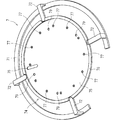
- FIG. 2 is a perspective view showing the entire appearance of the holder 7.
- the holding unit 7 is configured to include a base ring 71, a connecting unit 72, and a susceptor 74.
- the base ring 71, the connecting portion 72 and the susceptor 74 are all formed of quartz. That is, the whole of the holding portion 7 is formed of quartz.
- the base ring 71 is an arc-shaped quartz member which is partially missing from the annular shape. This missing portion is provided to prevent interference between the transfer arm 11 of the transfer mechanism 10 described later and the base ring 71.
- the base ring 71 is supported by the wall surface of the chamber 6 by being placed on the bottom of the recess 62 (see FIG. 1).
- On the top surface of the base ring 71 a plurality of connecting portions 72 (four in the present embodiment) are provided upright along the circumferential direction of the annular shape.
- the connecting portion 72 is also a quartz member and is fixed to the base ring 71 by welding.
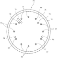
- FIG. 3 is a plan view of the susceptor 74.
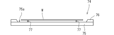
- FIG. 4 is a cross-sectional view of the susceptor 74.
- the susceptor 74 includes a holding plate 75, a guide ring 76 and a plurality of substrate support pins 77.
- the holding plate 75 is a substantially circular flat member made of quartz. The diameter of the holding plate 75 is larger than the diameter of the semiconductor wafer W. That is, the holding plate 75 has a larger planar size than the semiconductor wafer W.
- a guide ring 76 is installed on the upper surface peripheral portion of the holding plate 75.
- the guide ring 76 is an annular member having an inner diameter larger than the diameter of the semiconductor wafer W. For example, when the diameter of the semiconductor wafer W is ⁇ 300 mm, the inner diameter of the guide ring 76 is ⁇ 320 mm.
- the inner periphery of the guide ring 76 is tapered so as to widen upward from the holding plate 75.
- the guide ring 76 is formed of quartz similar to the holding plate 75.
- the guide ring 76 may be welded to the upper surface of the holding plate 75 or may be fixed to the holding plate 75 by a separately processed pin or the like. Alternatively, the holding plate 75 and the guide ring 76 may be processed as an integral member.
- a region of the upper surface of the holding plate 75 inside the guide ring 76 is a planar holding surface 75 a for holding the semiconductor wafer W.
- a plurality of substrate support pins 77 are provided upright on the holding surface 75 a of the holding plate 75. In the present embodiment, a total of 12 substrate support pins 77 are erected every 30 ° along the circumference of a concentric circle with the outer circumference circle of the holding surface 75a (the inner circumference circle of the guide ring 76).
- the diameter of the circle in which the 12 substrate support pins 77 are arranged (the distance between the opposing substrate support pins 77) is smaller than the diameter of the semiconductor wafer W, and if the diameter of the semiconductor wafer W is ⁇ 300 mm, ⁇ 270 mm to ⁇ 280 mm (this embodiment) The form is ⁇ 270 mm).
- Each substrate support pin 77 is formed of quartz.
- the plurality of substrate support pins 77 may be provided on the upper surface of the holding plate 75 by welding, or may be processed integrally with the holding plate 75.
- the four connecting portions 72 erected on the base ring 71 and the peripheral portion of the holding plate 75 of the susceptor 74 are fixed by welding. That is, the susceptor 74 and the base ring 71 are fixedly connected by the connecting portion 72.
- the holder 7 is attached to the chamber 6.
- the holding plate 75 of the susceptor 74 is in a horizontal posture (a posture in which the normal line coincides with the vertical direction). That is, the holding surface 75a of the holding plate 75 is a horizontal surface.
- the semiconductor wafer W carried into the chamber 6 is placed and held in a horizontal posture on the susceptor 74 of the holding unit 7 mounted in the chamber 6. At this time, the semiconductor wafer W is supported by the twelve substrate support pins 77 erected on the holding plate 75 and held by the susceptor 74. More strictly, the upper end portions of the twelve substrate support pins 77 contact the lower surface of the semiconductor wafer W to support the semiconductor wafer W. Since the heights of the twelve substrate support pins 77 (the distance from the upper end of the substrate support pins 77 to the holding surface 75 a of the holding plate 75) are uniform, the semiconductor wafer W is horizontally oriented by the twelve substrate support pins 77. It can be supported.
- the semiconductor wafer W is supported by the plurality of substrate support pins 77 at a predetermined distance from the holding surface 75 a of the holding plate 75.
- the thickness of the guide ring 76 is larger than the height of the substrate support pin 77. Therefore, the horizontal displacement of the semiconductor wafer W supported by the plurality of substrate support pins 77 is prevented by the guide ring 76.
- the holding plate 75 of the susceptor 74 is formed with an opening 78 penetrating therethrough in the vertical direction.
- the opening 78 is provided for the radiation thermometer 120 (see FIG. 1) to receive radiation (infrared light) emitted from the lower surface of the semiconductor wafer W. That is, the radiation thermometer 120 receives the light emitted from the lower surface of the semiconductor wafer W through the opening 78, and the temperature of the semiconductor wafer W is measured by a separate detector.
- four through holes 79 are formed in the holding plate 75 of the susceptor 74 so that lift pins 12 of the transfer mechanism 10 described later pass therethrough for delivery of the semiconductor wafer W.
- FIG. 5 is a plan view of the transfer mechanism 10.
- 6 is a side view of the transfer mechanism 10.
- the transfer mechanism 10 includes two transfer arms 11.
- the transfer arm 11 has an arc shape along the generally annular recess 62.
- Two lift pins 12 are erected on each transfer arm 11.
- the transfer arm 11 and the lift pin 12 are formed of quartz.
- Each transfer arm 11 is rotatable by a horizontal movement mechanism 13.
- the horizontal movement mechanism 13 transfers the pair of transfer arms 11 to the holding unit 7 at the transfer operation position (solid line position in FIG. 5) for transferring the semiconductor wafer W and the semiconductor wafer W held by the holding unit 7.
- Horizontal movement is performed between a retracted position (two-dot chain line position in FIG. 5) which does not overlap in plan view.
- each transfer arm 11 may be rotated by an individual motor, or a pair of transfer arms 11 may be interlocked by one motor using a link mechanism. It may be moved.
- the pair of transfer arms 11 are moved up and down together with the horizontal movement mechanism 13 by the elevation mechanism 14.
- the lifting mechanism 14 lifts the pair of transfer arms 11 at the transfer operation position, a total of four lift pins 12 pass through the through holes 79 (see FIGS. 2 and 3) formed in the susceptor 74 and lift pins The upper end of 12 protrudes from the upper surface of the susceptor 74.
- the lifting mechanism 14 lowers the pair of transfer arms 11 at the transfer operation position to extract the lift pins 12 from the through holes 79 and the horizontal movement mechanism 13 moves the pair of transfer arms 11 to open.
- the transfer arm 11 moves to the retracted position.
- the retracted position of the pair of transfer arms 11 is immediately above the base ring 71 of the holder 7.
- the radiation thermometer 120 measures the temperature of the semiconductor wafer W through the opening 78 provided in the susceptor 74.
- the radiation thermometer 130 detects the infrared light emitted from the upper chamber window 63 to measure the temperature of the upper chamber window 63.
- the radiation thermometer 140 detects infrared light emitted from the lower chamber window 64 to measure the temperature of the lower chamber window 64.
- a flash heating unit 5 provided above the chamber 6 is provided inside the housing 51 so as to cover a light source consisting of a plurality of (30 in this embodiment) xenon flash lamps FL and the upper side of the light source And the reflector 52, and it comprises.
- a lamp light emission window 53 is attached to the bottom of the housing 51 of the flash heating unit 5.
- the lamp light emission window 53 which constitutes the floor of the flash heating unit 5 is a plate-like quartz window formed of quartz.
- the plurality of flash lamps FL are rod-shaped lamps each having a long cylindrical shape, and the longitudinal direction of each is along the main surface of the semiconductor wafer W held by the holder 7 (that is, along the horizontal direction) They are arranged in a plane so as to be parallel to each other. Therefore, the plane formed by the arrangement of the flash lamps FL is also a horizontal plane.
- the xenon flash lamp FL has a rod-like glass tube (discharge tube) in which xenon gas is enclosed and an anode and a cathode connected to a capacitor are disposed at both ends, and attached on the outer peripheral surface of the glass tube And a trigger electrode. Since xenon gas is an insulator electrically, no electricity flows in the glass tube under normal conditions even if charge is stored in the capacitor. However, when a high voltage is applied to the trigger electrode to break the insulation, the electricity stored in the capacitor instantaneously flows in the glass tube, and light is emitted by excitation of atoms or molecules of xenon at that time.
- the electrostatic energy stored in advance in the capacitor is converted into an extremely short light pulse of 0.1 milliseconds to 100 milliseconds. It is characterized in that it can emit extremely intense light as compared to a light source. That is, the flash lamp FL is a pulse light emitting lamp that emits light instantaneously in an extremely short time of less than one second. The light emission time of the flash lamp FL can be adjusted by the coil constant of the lamp power supply that supplies power to the flash lamp FL.
- the reflector 52 is provided above the plurality of flash lamps FL so as to cover the whole of them.
- the basic function of the reflector 52 is to reflect flash light emitted from a plurality of flash lamps FL to the side of the heat treatment space 65.
- the reflector 52 is formed of an aluminum alloy plate, and its surface (surface facing the flash lamp FL) is roughened by blasting.
- the halogen heating unit 4 provided below the chamber 6 incorporates a plurality of (40 in the present embodiment) halogen lamps HL inside the housing 41.
- the halogen heating unit 4 is a light irradiation unit that heats the semiconductor wafer W by performing light irradiation on the heat treatment space 65 from the lower side of the chamber 6 through the lower chamber window 64 with a plurality of halogen lamps HL.
- the halogen heating unit 4 is disposed below the chamber 6 so that the plurality of halogen lamps HL face the lower chamber window 64.
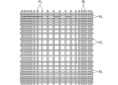
- FIG. 7 is a plan view showing the arrangement of the plurality of halogen lamps HL.
- the 40 halogen lamps HL are divided into upper and lower two stages.
- the twenty halogen lamps HL are disposed in the upper stage near the holding unit 7, and the twenty halogen lamps HL are disposed in the lower stage further from the holding unit 7 than the upper stage.
- Each halogen lamp HL is a rod-shaped lamp having a long cylindrical shape.
- the upper and lower 20 halogen lamps HL are arranged such that their longitudinal directions are parallel to each other along the main surface of the semiconductor wafer W held by the holder 7 (that is, along the horizontal direction). There is. Therefore, the plane formed by the arrangement of the halogen lamps HL in the upper and lower stages is a horizontal plane.
- the disposition density of the halogen lamps HL in the region facing the peripheral portion is higher than the region facing the central portion of the semiconductor wafer W held by the holding portion 7 in both the upper and lower portions. There is. That is, in both the upper and lower portions, the disposition pitch of the halogen lamps HL is shorter in the peripheral portion than in the central portion of the lamp arrangement. For this reason, it is possible to perform irradiation of a larger amount of light at the peripheral portion of the semiconductor wafer W which is likely to cause a temperature drop during heating by light irradiation from the halogen heating unit 4.
- a lamp group consisting of the halogen lamp HL in the upper stage and a lamp group consisting of the halogen lamp HL in the lower stage are arranged so as to cross in a lattice shape. That is, a total of 40 halogen lamps HL are disposed so that the longitudinal direction of the 20 halogen lamps HL disposed in the upper stage and the longitudinal direction of the 20 halogen lamps HL disposed in the lower stage are orthogonal to each other. There is.
- the halogen lamp HL is a filament type light source which causes the filament to glow to emit light by energizing the filament disposed inside the glass tube. Inside the glass tube, a gas in which a small amount of a halogen element (iodine, bromine or the like) is introduced into an inert gas such as nitrogen or argon is enclosed. By introducing a halogen element, it is possible to set the temperature of the filament to a high temperature while suppressing the breakage of the filament. Therefore, the halogen lamp HL has a characteristic that it has a long life and can continuously emit strong light as compared with a normal incandescent lamp. That is, the halogen lamp HL is a continuous lighting lamp which emits light continuously for at least one second or more. Further, since the halogen lamp HL is a rod-like lamp, it has a long life, and by arranging the halogen lamp HL in the horizontal direction, the radiation efficiency to the upper semiconductor wafer W becomes excellent.
- a halogen element
- a reflector 43 is provided below the two-stage halogen lamp HL also in the housing 41 of the halogen heating unit 4 (FIG. 1).
- the reflector 43 reflects the light emitted from the plurality of halogen lamps HL to the side of the heat treatment space 65.
- the control unit 3 controls the above-described various operation mechanisms provided in the heat treatment apparatus 1.
- the hardware configuration of the control unit 3 is the same as that of a general computer. That is, the control unit 3 includes a CPU that is a circuit that performs various arithmetic processing, a ROM that is a read only memory that stores a basic program, a RAM that is a readable and writable memory that stores various information, control software, data, and the like. It has a magnetic disk to be stored.
- the CPU of the control unit 3 executes a predetermined processing program to advance the processing in the heat treatment apparatus 1.
- the processing operation in the heat treatment apparatus 1 will be described.
- a normal heat treatment procedure for a semiconductor wafer W to be treated will be described.
- the semiconductor wafer W to be treated is a semiconductor substrate to which impurities (ions) are added by ion implantation.
- the activation of the impurities is performed by the flash light irradiation heat treatment (annealing) by the heat treatment apparatus 1.
- the processing procedure of the semiconductor wafer W described below proceeds with the control unit 3 controlling each operation mechanism of the heat treatment apparatus 1.
- the valve 84 for air supply is opened, and the valves 89 and 192 for exhaust are opened to start air supply / exhaust into the chamber 6.
- nitrogen gas is supplied from the gas supply holes 81 to the heat treatment space 65 as a processing gas.
- the valve 89 is opened, the gas in the chamber 6 is exhausted from the gas exhaust hole 86. Thereby, the nitrogen gas supplied from the upper part of the heat treatment space 65 in the chamber 6 flows downward, and is exhausted from the lower part of the heat treatment space 65.
- the gas in the chamber 6 is also exhausted from the transfer opening 66. Furthermore, the atmosphere around the drive unit of the transfer mechanism 10 is also exhausted by an exhaust mechanism (not shown). During the heat treatment of the semiconductor wafer W in the heat treatment apparatus 1, nitrogen gas is continuously supplied to the heat treatment space 65, and the supply amount thereof is appropriately changed in accordance with the treatment process.
- the gate valve 185 is opened, the transfer opening 66 is opened, and the semiconductor wafer W to be processed is carried into the heat treatment space 65 in the chamber 6 through the transfer opening 66 by the transfer robot outside the apparatus.
- the atmosphere outside the apparatus may be involved as the semiconductor wafer W is carried in, but since nitrogen gas continues to be supplied to the chamber 6, nitrogen gas flows out from the transfer opening 66, Of the external atmosphere can be minimized.
- the semiconductor wafer W carried in by the transfer robot advances to a position immediately above the holding unit 7 and stops there. Then, when the pair of transfer arms 11 of the transfer mechanism 10 horizontally move from the retracted position to the transfer operation position and ascends, the lift pins 12 protrude from the upper surface of the holding plate 75 of the susceptor 74 through the through holes 79. Semiconductor wafer W. At this time, the lift pin 12 ascends above the upper end of the substrate support pin 77.
- the transfer robot exits the heat treatment space 65, and the transfer opening 66 is closed by the gate valve 185. Then, when the pair of transfer arms 11 is lowered, the semiconductor wafer W is transferred from the transfer mechanism 10 to the susceptor 74 of the holding unit 7 and held horizontally from below.
- the semiconductor wafer W is supported by a plurality of substrate support pins 77 erected on the holding plate 75 and held by the susceptor 74.
- the semiconductor wafer W is held by the holding unit 7 with the surface on which the pattern formation is performed and the impurity is implanted as the upper surface.
- a predetermined distance is formed between the back surface (main surface opposite to the front surface) of the semiconductor wafer W supported by the plurality of substrate support pins 77 and the holding surface 75 a of the holding plate 75.
- the pair of transfer arms 11 lowered to the lower side of the susceptor 74 is retracted by the horizontal movement mechanism 13 to the retracted position, that is, to the inside of the recess 62.
- the 40 halogen lamps HL of the halogen heating unit 4 are simultaneously turned on to perform preheating (assist heating ) Is started.
- the halogen light emitted from the halogen lamp HL is transmitted to the lower surface of the semiconductor wafer W through the lower chamber window 64 and the susceptor 74 formed of quartz.
- the semiconductor wafer W is preheated by receiving light irradiation from the halogen lamp HL, and the temperature rises.
- the transfer arm 11 of the transfer mechanism 10 is retracted to the inside of the concave portion 62, there is no hindrance to the heating by the halogen lamp HL.
- the temperature of the semiconductor wafer W is measured by the radiation thermometer 120. That is, the radiation thermometer 120 receives infrared light emitted from the lower surface of the semiconductor wafer W held by the susceptor 74 through the opening 78, and measures the temperature of the wafer during temperature rise. The measured temperature of the semiconductor wafer W is transmitted to the control unit 3.
- the control unit 3 controls the output of the halogen lamp HL while monitoring whether or not the temperature of the semiconductor wafer W heated by irradiation of light from the halogen lamp HL has reached a predetermined preheating temperature T1.
- the control unit 3 feedback-controls the output of the halogen lamp HL so that the temperature of the semiconductor wafer W becomes the preheating temperature T1.
- the preheating temperature T1 is set to about 200 ° C. to 800 ° C., preferably about 350 ° C. to 600 ° C. (in this embodiment, 600 ° C.) without the risk that the impurity added to the semiconductor wafer W is diffused by heat. .
- the control unit 3 After the temperature of the semiconductor wafer W reaches the preheating temperature T1, the control unit 3 temporarily maintains the semiconductor wafer W at the preheating temperature T1. Specifically, when the temperature of the semiconductor wafer W measured by the radiation thermometer 120 reaches the preheating temperature T1, the control unit 3 adjusts the output of the halogen lamp HL to substantially reserve the temperature of the semiconductor wafer W. The heating temperature T1 is maintained.
- the flash lamp FL of the flash heating unit 5 performs flash light irradiation on the surface of the semiconductor wafer W held by the susceptor 74. At this time, a part of the flash light emitted from the flash lamp FL directly goes into the chamber 6, and the other part is once reflected by the reflector 52 and then goes into the chamber 6, and these flash lights are Flash heating of the semiconductor wafer W is performed by the irradiation.
- the surface temperature of the semiconductor wafer W can be raised in a short time. That is, the flash light emitted from the flash lamp FL has an extremely short irradiation time of 0.1 milliseconds or more and 100 milliseconds or less, in which electrostatic energy previously stored in the capacitor is converted into an extremely short light pulse. It is a strong flashlight. Then, the surface temperature of the semiconductor wafer W flash-heated by the flash light irradiation from the flash lamp FL instantaneously rises to the processing temperature T2 of 1000 ° C. or higher, and the impurity implanted into the semiconductor wafer W is activated. After that, the surface temperature drops rapidly.
- the heat treatment apparatus 1 can raise and lower the surface temperature of the semiconductor wafer W in a very short time, the activation of the impurities is suppressed while the diffusion of the impurities injected into the semiconductor wafer W is suppressed. Can. Since the time required for activating the impurity is extremely short compared to the time required for its thermal diffusion, the activation can be performed even for a short time when diffusion of about 0.1 milliseconds to 100 milliseconds does not occur. Complete.
- the halogen lamp HL is turned off after a predetermined time has elapsed. Thereby, the semiconductor wafer W is rapidly cooled from the preheating temperature T1.
- the temperature of the semiconductor wafer W being cooled is measured by the radiation thermometer 120, and the measurement result is transmitted to the control unit 3.
- the control unit 3 monitors whether the temperature of the semiconductor wafer W has dropped to a predetermined temperature based on the measurement result of the radiation thermometer 120.
- the pair of transfer arms 11 of the transfer mechanism 10 horizontally move from the retracted position to the transfer operation position again and rises, whereby the lift pins 12 are susceptors
- the semiconductor wafer W after heat treatment is projected from the upper surface of the substrate 74 from the susceptor 74.
- the transfer opening 66 closed by the gate valve 185 is opened, the semiconductor wafer W placed on the lift pins 12 is carried out by the transfer robot outside the apparatus, and the heat treatment of the semiconductor wafer W in the heat treatment apparatus 1 is performed. Is complete.
- the processing of the semiconductor wafer W is performed in lot units.
- a lot is a set of semiconductor wafers W to be subjected to processing of the same contents under the same conditions.
- a plurality of (for example, 25) semiconductor wafers W constituting a lot are sequentially carried into the chamber 6 one by one and heat treatment is performed.
- the first semiconductor wafer W of the lot is carried into the chamber 6 at approximately room temperature, and flash heat treatment is performed.
- heat conduction and heat radiation from the semiconductor wafer W heated up to the chamber internal structure such as the susceptor 74 occur, so that the number of semiconductor wafers W processed in the chamber internal structure initially increased at room temperature increases.
- the temperature of the internal structure including the lower chamber window 64 reaches a certain stable temperature.
- the amount of heat transfer from the semiconductor wafer W to the internal structure of the chamber balances with the amount of heat released from the internal structure of the chamber. Since the amount of heat transfer from the semiconductor wafer W is larger than the amount of heat radiated from the chamber internal structure until the temperature of the chamber 6 reaches the stable temperature, the temperature of the chamber internal structure increases as the number of processed semiconductor wafers W increases. Gradually increase due to heat storage.
- the heat transfer amount from the semiconductor wafer W and the heat release amount from the chamber internal structure are balanced, so the temperature of the chamber internal structure is constant and stable. It will be maintained at the temperature. Also, after the temperature of the lower chamber window 64 reaches the stable temperature, the amount of heat absorbed by the lower chamber window 64 from the irradiation light of the halogen lamp HL and the amount of heat released from the lower chamber window 64 are balanced. The temperature of the lower chamber window 64 is also maintained at a constant stable temperature.
- the temperature of the structure of the chamber 6 is different between the initial semiconductor wafer W of the lot and the semiconductor wafer W halfway.
- the semiconductor wafer W in the initial stage of the lot is processed in the chamber 6 near room temperature
- the semiconductor wafer W after the tenth wafer is in the chamber 6 which is heated to a stable temperature. Will be processed.
- the semiconductor wafer W in the initial stage of the lot and the semiconductor wafer W in the middle of the lot have a problem that the temperature history becomes uneven because the peripheral temperature is different.
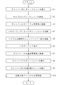
- FIG. 8 is a flowchart showing the processing procedure of the heat treatment method according to the present invention.
- the dummy wafer DW is loaded into the chamber 6 (step S1).
- the dummy wafer DW is a disk-shaped silicon wafer similar to the semiconductor wafer W, and has the same size and shape as the semiconductor wafer W. However, the dummy wafer DW is not subjected to pattern formation or ion implantation (so-called bare wafer).
- the loading procedure of the dummy wafer DW into the chamber 6 is the same as the loading procedure of the semiconductor wafer W described above. That is, the dummy wafer DW is carried into the chamber 6 by the transfer robot outside the apparatus, and the lift pins 12 of the transfer mechanism 10 receive the dummy wafer DW. Then, the lift pins 12 are lowered to hold the dummy wafer DW on the susceptor 74 (step S2). In addition, at the time of carrying in of dummy wafer DW, the inside of chamber 6 is made into nitrogen atmosphere.
- step S3 the inside of the chamber 6 is replaced with a helium atmosphere.
- the atmosphere of the heat treatment space 65 which is a closed space, is exhausted without performing any gas supply from the gas supply holes 81 to depressurize the inside of the chamber 6 to less than the atmospheric pressure.
- the valve 89 and the valve 192 are closed, the valve 84 is opened, and a mixed gas of helium and nitrogen is supplied from the gas supply source 85 into the chamber 6.
- an atmosphere containing helium gas is formed in the heat treatment space 65 in the chamber 6.
- the 40 halogen lamps HL are turned on, and the dummy wafer DW is heated by light irradiation from the halogen lamps HL (step S4).
- the light emitted from the halogen lamp HL passes through the lower chamber window 64 and the susceptor 74 formed of quartz and is irradiated to the lower surface of the dummy wafer DW.
- the dummy wafer DW is heated by receiving light irradiation from the halogen lamp HL and its temperature rises.
- FIG. 9 is a view showing a state in which the dummy wafer DW is heated in a helium atmosphere.
- Helium gas has a higher thermal conductivity than nitrogen gas, which is a processing gas used during heat treatment of the semiconductor wafer W.
- the thermal conductivity of helium gas at 0 ° C. is 0.144 W / mK, while the thermal conductivity of nitrogen gas at 0 ° C. is 0.024 W / mK.
- the helium gas having such a high thermal conductivity functions as a heat transfer gas, and when the temperature of the dummy wafer DW rises in the atmosphere containing the helium gas, the helium gas is used as a heat transfer medium from the dummy wafer DW in the chamber 6 Heat transfer occurs in the structure. Thereby, the upper chamber window 63 and the lower chamber window 64 of the chamber 6 are heated (step S5). The susceptor 74 is also heated by heat conduction and heat radiation from the heated dummy wafer DW.
- the structure in the chamber 6 is heated by the dummy wafer DW so that the temperatures of the upper chamber window 63 and the lower chamber window 64 reach the stable temperature.
- the stable temperature of the upper chamber window 63 and the lower chamber window 64 means that the temperature of the upper chamber window 63 and the lower chamber window 64 rises after the heat treatment of 10 or more semiconductor wafers W of the lot is continuously performed.
- the output of the halogen lamp HL capable of heating the dummy wafer DW to a temperature necessary to raise the upper chamber window 63 and the lower chamber window 64 to a stable temperature is previously determined by experiment or simulation Set in the control unit 3.
- the output of the halogen lamp HL is adjusted to the set output.
- the dummy wafer DW is heated to a predetermined temperature by light irradiation from the halogen lamp HL, and the upper chamber window 63 and the lower chamber window 64 are heated to a stable temperature from the dummy wafer DW using helium gas as a heat medium.
- the control unit 3 performs feedback control of the output of the halogen lamp HL so that the upper chamber window 63 and the lower chamber window 64 have stable temperatures. Also good.
- step S6 After the upper chamber window 63 and the lower chamber window 64 are heated to a stable temperature by the dummy wafer DW, the 40 halogen lamps HL are extinguished (step S6). Although the temperature of the dummy wafer DW is lowered by turning off the halogen lamp HL, the upper chamber window 63, the lower chamber window 64 and the quartz member of the susceptor 74 having a large heat capacity are not stabilized immediately but are almost stabilized. Maintained.
- step S7 the inside of the chamber 6 is replaced with a nitrogen atmosphere.
- the inside of the chamber 6 is rapidly replaced from the helium atmosphere to the nitrogen atmosphere by temporarily reducing the pressure in the chamber 6 below atmospheric pressure and supplying nitrogen gas.
- the dummy wafer DW is unloaded from the chamber 6 (step S8).
- the procedure for unloading the dummy wafer DW from the chamber 6 is also the same as the procedure for unloading the semiconductor wafer W described above. That is, the lift pins 12 ascend to receive the dummy wafer DW from the susceptor 74, and the dummy wafer DW is unloaded from the chamber 6 by the transfer robot outside the apparatus.
- the semiconductor wafer W to be processed first in the lot is loaded into the chamber 6 and held on the susceptor 74 (step S9). Then, the heat treatment of the semiconductor wafer W to be processed is performed along the above-described processing procedure (step S10).
- the dummy wafer DW is carried into the chamber 6 and placed on the susceptor 74 before starting the processing of the semiconductor wafer W to be first processed in the lot, and the heat conduction is higher than nitrogen gas.
- Helium gas having a ratio is supplied into the chamber 6 to form an atmosphere containing helium gas.
- the dummy wafer DW is heated by irradiation of light from the halogen lamp HL in an atmosphere containing helium gas, whereby the upper chamber window 63 and the lower chamber window 64 with the helium gas as a heat medium from the heated dummy wafer DW.
- the heat conduction occurs in the structure in the chamber 6 including the Particularly, by setting the inside of the chamber 6 to an atmosphere containing helium gas having high thermal conductivity, the heat of the dummy wafer DW is efficiently transferred to the structure in the chamber 6 including the upper chamber window 63 and the lower chamber window 64. It can be done.
- the temperature of the structure is raised, thereby making it possible to process the first batch of the lot.
- the upper chamber window 63 and the lower chamber window 64 are heated to a stable temperature. Therefore, the upper chamber window 63 and the lower chamber window 64 have the same temperature (stable temperature) over all the semiconductor wafers W constituting the lot, and the temperature history can be made uniform.
- the present invention is not limited to this.
- the heat transfer gas may be any gas having a thermal conductivity higher than that of nitrogen gas, which is a processing gas used in heat treatment of the semiconductor wafer W to be treated.
- hydrogen gas thermal conductivity at 0 ° C. 0.168 W / mK
- plural kinds of heat transfer gases may be mixed and supplied into the chamber 6.
- the mixing ratio of the heat transfer gas can be changed by a mass flow controller or the like.
- the heat transfer gas such as helium gas may be heated by the heater 22 and supplied into the chamber 6.
- the structure in the chamber 6 including the upper chamber window 63 and the lower chamber window 64 can be heated more efficiently.
- the number of flash lamps FL can be made into arbitrary numbers.
- the flash lamp FL is not limited to the xenon flash lamp, and may be a krypton flash lamp.
- the number of halogen lamps HL provided in the halogen heating unit 4 is not limited to 40, and can be an arbitrary number.
- the preheating of the semiconductor wafer W is performed using the filament type halogen lamp HL as a continuous lighting lamp that emits light continuously for 1 second or more, but the present invention is not limited to this.
- a discharge type arc lamp for example, a xenon arc lamp
- the dummy wafer DW is heated by the discharge type arc lamp at the time of preheating.
- the substrate to be treated by the heat treatment apparatus 1 is not limited to a semiconductor wafer, and may be a glass substrate used for a flat panel display such as a liquid crystal display device or a substrate for a solar cell. Further, the technique according to the present invention may be applied to heat treatment of a high dielectric constant gate insulating film (High-k film), bonding of metal and silicon, or crystallization of polysilicon.
- High-k film high dielectric constant gate insulating film
- the heat treatment technique according to the present invention is not limited to the flash lamp annealing apparatus, and is also applied to an apparatus of a heat source other than a single wafer type lamp annealing apparatus using a halogen lamp and a flash lamp such as a CVD apparatus. be able to.
- the technology according to the present invention can be suitably applied to a backside annealing apparatus in which a halogen lamp is disposed below the chamber and light is irradiated from the back surface of the semiconductor wafer to perform heat treatment.
Landscapes
- Container, Conveyance, Adherence, Positioning, Of Wafer (AREA)
- Health & Medical Sciences (AREA)
- Toxicology (AREA)
Abstract
Description
3 制御部
4 ハロゲン加熱部
5 フラッシュ加熱部
6 チャンバー
7 保持部
10 移載機構
22 ヒータ
63 上側チャンバー窓
64 下側チャンバー窓
65 熱処理空間
74 サセプタ
84 バルブ
85 ガス供給源
120,130,140 放射温度計
DW ダミーウェハー
FL フラッシュランプ
HL ハロゲンランプ
W 半導体ウェハー
Claims (6)
- 基板に光を照射することによって該基板を加熱する熱処理方法であって、
チャンバー内のサセプタに載置された基板に連続点灯ランプから光を照射して当該基板を加熱する光照射工程と、
処理対象となる基板を前記チャンバーに搬入する前に、前記サセプタに予熱用基板を載置し、前記光照射工程にて使用する処理ガスよりも熱伝導率の高い伝熱ガスを前記チャンバー内に供給して前記伝熱ガスを含む雰囲気を形成する雰囲気形成工程と、
前記連続点灯ランプからの光照射によって前記予熱用基板を加熱し、前記予熱用基板から前記伝熱ガスを介して前記チャンバーに設けられた石英窓を昇温する予熱工程と、
を備える熱処理方法。 - 請求項1記載の熱処理方法において、
前記雰囲気形成工程では、加熱された前記伝熱ガスを前記チャンバー内に供給する熱処理方法。 - 請求項1または請求項2記載の熱処理方法において、
前記伝熱ガスがヘリウムである熱処理方法。 - 基板に光を照射することによって該基板を加熱する熱処理装置であって、
基板を収容するチャンバーと、
前記チャンバー内にて基板を支持するサセプタと、
前記サセプタに支持された基板に光を照射して当該基板を加熱する連続点灯ランプと、
前記チャンバー内にガスを供給するガス供給部と、
を備え、
処理対象となる基板を前記チャンバーに搬入する前に、前記サセプタに予熱用基板を載置し、前記処理対象となる基板の熱処理時に使用する処理ガスよりも熱伝導率の高い伝熱ガスを前記ガス供給部から前記チャンバー内に供給して前記伝熱ガスを含む雰囲気を形成した後、前記連続点灯ランプからの光照射によって前記予熱用基板を加熱して前記予熱用基板から前記伝熱ガスを介して前記チャンバーに設けられた石英窓を昇温する熱処理装置。 - 請求項4記載の熱処理装置において、
前記伝熱ガスを加熱するガス加熱部をさらに備える熱処理装置。 - 請求項4または請求項5記載の熱処理装置において、
前記伝熱ガスがヘリウムである熱処理装置。
Priority Applications (3)
| Application Number | Priority Date | Filing Date | Title |
|---|---|---|---|
| CN201880086977.6A CN111656489B (zh) | 2018-01-26 | 2018-10-03 | 热处理方法及热处理装置 |
| US16/960,923 US11251057B2 (en) | 2018-01-26 | 2018-10-03 | Thermal processing method and thermal processing device |
| KR1020207021697A KR102407656B1 (ko) | 2018-01-26 | 2018-10-03 | 열처리 방법 및 열처리 장치 |
Applications Claiming Priority (2)
| Application Number | Priority Date | Filing Date | Title |
|---|---|---|---|
| JP2018011269A JP6960344B2 (ja) | 2018-01-26 | 2018-01-26 | 熱処理方法および熱処理装置 |
| JP2018-011269 | 2018-01-26 |
Publications (1)
| Publication Number | Publication Date |
|---|---|
| WO2019146166A1 true WO2019146166A1 (ja) | 2019-08-01 |
Family
ID=67395309
Family Applications (1)
| Application Number | Title | Priority Date | Filing Date |
|---|---|---|---|
| PCT/JP2018/037010 Ceased WO2019146166A1 (ja) | 2018-01-26 | 2018-10-03 | 熱処理方法および熱処理装置 |
Country Status (6)
| Country | Link |
|---|---|
| US (1) | US11251057B2 (ja) |
| JP (1) | JP6960344B2 (ja) |
| KR (1) | KR102407656B1 (ja) |
| CN (1) | CN111656489B (ja) |
| TW (1) | TWI696221B (ja) |
| WO (1) | WO2019146166A1 (ja) |
Cited By (3)
| Publication number | Priority date | Publication date | Assignee | Title |
|---|---|---|---|---|
| US20220037164A1 (en) * | 2020-07-31 | 2022-02-03 | SCREEN Holdings Co., Ltd. | Light irradiation type heat treatment method |
| US11251057B2 (en) * | 2018-01-26 | 2022-02-15 | SCREEN Holdings Co., Ltd. | Thermal processing method and thermal processing device |
| CN114823427A (zh) * | 2022-05-30 | 2022-07-29 | 北京北方华创微电子装备有限公司 | 半导体工艺设备及其预热腔室 |
Families Citing this family (1)
| Publication number | Priority date | Publication date | Assignee | Title |
|---|---|---|---|---|
| JP7091221B2 (ja) * | 2018-10-23 | 2022-06-27 | 株式会社Screenホールディングス | 熱処理方法および熱処理装置 |
Citations (6)
| Publication number | Priority date | Publication date | Assignee | Title |
|---|---|---|---|---|
| JPH07235507A (ja) * | 1994-02-25 | 1995-09-05 | Toshiba Corp | 半導体装置の製造方法 |
| JPH09156916A (ja) * | 1995-11-29 | 1997-06-17 | Semiconductor Energy Lab Co Ltd | 多結晶珪素作製装置およびその動作方法 |
| WO1997022142A1 (en) * | 1995-12-14 | 1997-06-19 | Seiko Epson Corporation | Thin film semiconductor device, method for manufacturing thin film semiconductor device, liquid crystal display, method for manufacturing liquid crystal display, electronic apparatus, method for manufacturing electronic apparatus, and method for depositing thin film |
| JPH09162124A (ja) * | 1995-12-09 | 1997-06-20 | Semiconductor Energy Lab Co Ltd | 半導体処理方法 |
| JP2010225645A (ja) * | 2009-03-19 | 2010-10-07 | Dainippon Screen Mfg Co Ltd | 熱処理装置 |
| JP2018148178A (ja) * | 2017-03-09 | 2018-09-20 | 株式会社Screenホールディングス | 熱処理方法 |
Family Cites Families (30)
| Publication number | Priority date | Publication date | Assignee | Title |
|---|---|---|---|---|
| US6391690B2 (en) * | 1995-12-14 | 2002-05-21 | Seiko Epson Corporation | Thin film semiconductor device and method for producing the same |
| KR100203780B1 (ko) | 1996-09-23 | 1999-06-15 | 윤종용 | 반도체 웨이퍼 열처리 장치 |
| US7127367B2 (en) * | 2003-10-27 | 2006-10-24 | Applied Materials, Inc. | Tailored temperature uniformity |
| US8536492B2 (en) | 2003-10-27 | 2013-09-17 | Applied Materials, Inc. | Processing multilayer semiconductors with multiple heat sources |
| US20080090309A1 (en) * | 2003-10-27 | 2008-04-17 | Ranish Joseph M | Controlled annealing method |
| JP4371260B2 (ja) * | 2003-12-01 | 2009-11-25 | 大日本スクリーン製造株式会社 | 熱処理装置 |
| US20140003800A1 (en) | 2004-09-24 | 2014-01-02 | Applied Materials, Inc. | Processing multilayer semiconductors with multiple heat sources |
| TWI395272B (zh) * | 2008-05-02 | 2013-05-01 | 應用材料股份有限公司 | 用於旋轉基板之非徑向溫度控制系統 |
| US9640412B2 (en) * | 2009-11-20 | 2017-05-02 | Applied Materials, Inc. | Apparatus and method for enhancing the cool down of radiatively heated substrates |
| JP5507274B2 (ja) * | 2010-01-29 | 2014-05-28 | 大日本スクリーン製造株式会社 | 熱処理方法および熱処理装置 |
| JP2013051281A (ja) * | 2011-08-30 | 2013-03-14 | Hitachi Kokusai Electric Inc | 基板処理装置 |
| JP5964626B2 (ja) * | 2012-03-22 | 2016-08-03 | 株式会社Screenホールディングス | 熱処理装置 |
| JP5996409B2 (ja) | 2012-12-12 | 2016-09-21 | 株式会社Screenホールディングス | 熱処理装置および熱処理方法 |
| JP6234674B2 (ja) * | 2012-12-13 | 2017-11-22 | 株式会社Screenホールディングス | 熱処理装置 |
| JP6009513B2 (ja) | 2014-09-02 | 2016-10-19 | 株式会社日立国際電気 | 半導体装置の製造方法、基板処理装置およびプログラム |
| JP6473659B2 (ja) * | 2015-05-13 | 2019-02-20 | 株式会社Screenホールディングス | 熱処理方法および熱処理装置 |
| JP2017017277A (ja) * | 2015-07-06 | 2017-01-19 | 株式会社Screenホールディングス | 熱処理装置および熱処理方法 |
| JP6560550B2 (ja) * | 2015-07-06 | 2019-08-14 | 株式会社Screenホールディングス | 熱処理方法および熱処理装置 |
| JP6654374B2 (ja) * | 2015-08-17 | 2020-02-26 | 株式会社Screenホールディングス | 熱処理方法および熱処理装置 |
| US10121683B2 (en) * | 2015-08-26 | 2018-11-06 | SCREEN Holdings Co., Ltd. | Light-irradiation heat treatment method and heat treatment apparatus |
| JP6598630B2 (ja) * | 2015-10-22 | 2019-10-30 | 株式会社Screenホールディングス | 熱処理方法 |
| JP6539568B2 (ja) * | 2015-11-04 | 2019-07-03 | 株式会社Screenホールディングス | 熱処理方法および熱処理装置 |
| JP2017139312A (ja) * | 2016-02-03 | 2017-08-10 | 株式会社Screenホールディングス | 接合形成方法 |
| CN109314046A (zh) * | 2016-09-23 | 2019-02-05 | 株式会社国际电气 | 基板处理装置、半导体装置的制造方法以及记录介质 |
| JP6894256B2 (ja) * | 2017-02-23 | 2021-06-30 | 株式会社Screenホールディングス | 熱処理方法および熱処理装置 |
| JP6864552B2 (ja) * | 2017-05-17 | 2021-04-28 | 株式会社Screenホールディングス | 熱処理装置および熱処理方法 |
| US10571337B2 (en) * | 2017-05-26 | 2020-02-25 | Applied Materials, Inc. | Thermal cooling member with low temperature control |
| WO2019147405A1 (en) * | 2018-01-23 | 2019-08-01 | Applied Materials, Inc. | Methods and apparatus for wafer temperature measurement |
| JP6960344B2 (ja) * | 2018-01-26 | 2021-11-05 | 株式会社Screenホールディングス | 熱処理方法および熱処理装置 |
| JP7179531B2 (ja) * | 2018-08-28 | 2022-11-29 | 株式会社Screenホールディングス | 熱処理方法 |
-
2018
- 2018-01-26 JP JP2018011269A patent/JP6960344B2/ja active Active
- 2018-10-03 KR KR1020207021697A patent/KR102407656B1/ko active Active
- 2018-10-03 WO PCT/JP2018/037010 patent/WO2019146166A1/ja not_active Ceased
- 2018-10-03 CN CN201880086977.6A patent/CN111656489B/zh active Active
- 2018-10-03 US US16/960,923 patent/US11251057B2/en active Active
- 2018-11-01 TW TW107138719A patent/TWI696221B/zh active
Patent Citations (6)
| Publication number | Priority date | Publication date | Assignee | Title |
|---|---|---|---|---|
| JPH07235507A (ja) * | 1994-02-25 | 1995-09-05 | Toshiba Corp | 半導体装置の製造方法 |
| JPH09156916A (ja) * | 1995-11-29 | 1997-06-17 | Semiconductor Energy Lab Co Ltd | 多結晶珪素作製装置およびその動作方法 |
| JPH09162124A (ja) * | 1995-12-09 | 1997-06-20 | Semiconductor Energy Lab Co Ltd | 半導体処理方法 |
| WO1997022142A1 (en) * | 1995-12-14 | 1997-06-19 | Seiko Epson Corporation | Thin film semiconductor device, method for manufacturing thin film semiconductor device, liquid crystal display, method for manufacturing liquid crystal display, electronic apparatus, method for manufacturing electronic apparatus, and method for depositing thin film |
| JP2010225645A (ja) * | 2009-03-19 | 2010-10-07 | Dainippon Screen Mfg Co Ltd | 熱処理装置 |
| JP2018148178A (ja) * | 2017-03-09 | 2018-09-20 | 株式会社Screenホールディングス | 熱処理方法 |
Cited By (4)
| Publication number | Priority date | Publication date | Assignee | Title |
|---|---|---|---|---|
| US11251057B2 (en) * | 2018-01-26 | 2022-02-15 | SCREEN Holdings Co., Ltd. | Thermal processing method and thermal processing device |
| US20220037164A1 (en) * | 2020-07-31 | 2022-02-03 | SCREEN Holdings Co., Ltd. | Light irradiation type heat treatment method |
| US11908703B2 (en) * | 2020-07-31 | 2024-02-20 | SCREEN Holdings Co., Ltd. | Light irradiation type heat treatment method |
| CN114823427A (zh) * | 2022-05-30 | 2022-07-29 | 北京北方华创微电子装备有限公司 | 半导体工艺设备及其预热腔室 |
Also Published As
| Publication number | Publication date |
|---|---|
| CN111656489B (zh) | 2025-01-07 |
| US11251057B2 (en) | 2022-02-15 |
| JP6960344B2 (ja) | 2021-11-05 |
| CN111656489A (zh) | 2020-09-11 |
| TW201933488A (zh) | 2019-08-16 |
| US20200335366A1 (en) | 2020-10-22 |
| JP2019129273A (ja) | 2019-08-01 |
| KR102407656B1 (ko) | 2022-06-10 |
| KR20200095578A (ko) | 2020-08-10 |
| TWI696221B (zh) | 2020-06-11 |
Similar Documents
| Publication | Publication Date | Title |
|---|---|---|
| KR102097200B1 (ko) | 열처리 방법 | |
| JP2017017277A (ja) | 熱処理装置および熱処理方法 | |
| JP6944347B2 (ja) | 熱処理装置および熱処理方法 | |
| JP7319894B2 (ja) | 熱処理装置 | |
| JP6864564B2 (ja) | 熱処理方法 | |
| CN110867370B (zh) | 热处理方法 | |
| JP7315331B2 (ja) | 熱処理方法および熱処理装置 | |
| JP2019009368A (ja) | 熱処理装置および熱処理方法 | |
| JP6622617B2 (ja) | 熱処理装置 | |
| JP2019220565A (ja) | 熱処理装置 | |
| CN114068326B (zh) | 热处理方法 | |
| TW202044412A (zh) | 熱處理裝置 | |
| TWI781350B (zh) | 熱處理方法及熱處理裝置 | |
| JP2018152405A (ja) | 熱処理方法および熱処理装置 | |
| JP6960344B2 (ja) | 熱処理方法および熱処理装置 | |
| TWI761908B (zh) | 熱處理方法及熱處理裝置 | |
| TW201740438A (zh) | 熱處理用承載器及熱處理裝置 | |
| JP7499160B2 (ja) | 熱処理方法 | |
| JP7211789B2 (ja) | 熱処理方法および熱処理装置 | |
| JP2022045565A (ja) | 熱処理装置 | |
| JP2017139313A (ja) | 熱処理用サセプタおよび熱処理装置 | |
| JP6539498B2 (ja) | 熱処理装置 | |
| JP2023030458A (ja) | 熱処理装置および熱処理方法 | |
| JP2021136376A (ja) | 熱処理方法 | |
| WO2020166249A1 (ja) | 熱処理方法および熱処理装置 |
Legal Events
| Date | Code | Title | Description |
|---|---|---|---|
| 121 | Ep: the epo has been informed by wipo that ep was designated in this application |
Ref document number: 18901893 Country of ref document: EP Kind code of ref document: A1 |
|
| ENP | Entry into the national phase |
Ref document number: 20207021697 Country of ref document: KR Kind code of ref document: A |
|
| NENP | Non-entry into the national phase |
Ref country code: DE |
|
| 122 | Ep: pct application non-entry in european phase |
Ref document number: 18901893 Country of ref document: EP Kind code of ref document: A1 |
|
| WWG | Wipo information: grant in national office |
Ref document number: 201880086977.6 Country of ref document: CN |