WO2019098165A1 - Metal plate for manufacturing vapor deposition mask and method for manufacturing metal plate, and vapor deposition mask and method for manufacturing vapor deposition mask - Google Patents
Metal plate for manufacturing vapor deposition mask and method for manufacturing metal plate, and vapor deposition mask and method for manufacturing vapor deposition mask Download PDFInfo
- Publication number
- WO2019098165A1 WO2019098165A1 PCT/JP2018/041915 JP2018041915W WO2019098165A1 WO 2019098165 A1 WO2019098165 A1 WO 2019098165A1 JP 2018041915 W JP2018041915 W JP 2018041915W WO 2019098165 A1 WO2019098165 A1 WO 2019098165A1
- Authority
- WO
- WIPO (PCT)
- Prior art keywords
- metal plate
- deposition mask
- manufacturing
- vapor deposition
- depression
- Prior art date
Links
- 229910052751 metal Inorganic materials 0.000 title claims abstract description 353
- 239000002184 metal Substances 0.000 title claims abstract description 353
- 238000007740 vapor deposition Methods 0.000 title claims abstract description 141
- 238000000034 method Methods 0.000 title claims abstract description 98
- 238000004519 manufacturing process Methods 0.000 title claims abstract description 72
- 238000007689 inspection Methods 0.000 claims abstract description 92
- 238000012937 correction Methods 0.000 claims description 145
- 230000008021 deposition Effects 0.000 claims description 90
- 230000008569 process Effects 0.000 claims description 70
- 238000005530 etching Methods 0.000 claims description 40
- PXHVJJICTQNCMI-UHFFFAOYSA-N Nickel Chemical compound [Ni] PXHVJJICTQNCMI-UHFFFAOYSA-N 0.000 claims description 34
- 238000005259 measurement Methods 0.000 claims description 29
- 229910000640 Fe alloy Inorganic materials 0.000 claims description 17
- 229910052759 nickel Inorganic materials 0.000 claims description 17
- 238000012545 processing Methods 0.000 claims description 17
- 238000004364 calculation method Methods 0.000 claims description 10
- 238000000151 deposition Methods 0.000 description 87
- 239000000463 material Substances 0.000 description 83
- 238000005096 rolling process Methods 0.000 description 80
- 238000000137 annealing Methods 0.000 description 54
- 239000000758 substrate Substances 0.000 description 51
- 238000012360 testing method Methods 0.000 description 17
- 239000003921 oil Substances 0.000 description 15
- 230000003746 surface roughness Effects 0.000 description 14
- 238000010586 diagram Methods 0.000 description 13
- 239000011347 resin Substances 0.000 description 12
- 229920005989 resin Polymers 0.000 description 12
- 230000000149 penetrating effect Effects 0.000 description 9
- XEEYBQQBJWHFJM-UHFFFAOYSA-N Iron Chemical compound [Fe] XEEYBQQBJWHFJM-UHFFFAOYSA-N 0.000 description 8
- 239000007789 gas Substances 0.000 description 8
- 239000011261 inert gas Substances 0.000 description 8
- 230000008018 melting Effects 0.000 description 8
- 238000002844 melting Methods 0.000 description 8
- 239000002826 coolant Substances 0.000 description 7
- 238000012986 modification Methods 0.000 description 7
- 230000004048 modification Effects 0.000 description 7
- 239000002994 raw material Substances 0.000 description 7
- 239000013256 coordination polymer Substances 0.000 description 6
- 238000009826 distribution Methods 0.000 description 6
- 238000000227 grinding Methods 0.000 description 5
- XKRFYHLGVUSROY-UHFFFAOYSA-N Argon Chemical compound [Ar] XKRFYHLGVUSROY-UHFFFAOYSA-N 0.000 description 4
- VEXZGXHMUGYJMC-UHFFFAOYSA-N Hydrochloric acid Chemical compound Cl VEXZGXHMUGYJMC-UHFFFAOYSA-N 0.000 description 4
- 238000004140 cleaning Methods 0.000 description 4
- 238000005137 deposition process Methods 0.000 description 4
- 229910052742 iron Inorganic materials 0.000 description 4
- 239000000047 product Substances 0.000 description 4
- 238000000926 separation method Methods 0.000 description 4
- 238000004804 winding Methods 0.000 description 4
- 230000015572 biosynthetic process Effects 0.000 description 3
- 238000000576 coating method Methods 0.000 description 3
- 230000002950 deficient Effects 0.000 description 3
- 238000005401 electroluminescence Methods 0.000 description 3
- 230000003628 erosive effect Effects 0.000 description 3
- 230000008020 evaporation Effects 0.000 description 3
- 238000001704 evaporation Methods 0.000 description 3
- 239000007788 liquid Substances 0.000 description 3
- 239000011368 organic material Substances 0.000 description 3
- 238000003466 welding Methods 0.000 description 3
- VYZAMTAEIAYCRO-UHFFFAOYSA-N Chromium Chemical compound [Cr] VYZAMTAEIAYCRO-UHFFFAOYSA-N 0.000 description 2
- UFHFLCQGNIYNRP-UHFFFAOYSA-N Hydrogen Chemical compound [H][H] UFHFLCQGNIYNRP-UHFFFAOYSA-N 0.000 description 2
- 229910001374 Invar Inorganic materials 0.000 description 2
- 229910021578 Iron(III) chloride Inorganic materials 0.000 description 2
- 229910045601 alloy Inorganic materials 0.000 description 2
- 239000000956 alloy Substances 0.000 description 2
- 238000004458 analytical method Methods 0.000 description 2
- 229910052786 argon Inorganic materials 0.000 description 2
- 230000008859 change Effects 0.000 description 2
- 229910052804 chromium Inorganic materials 0.000 description 2
- 239000011651 chromium Substances 0.000 description 2
- 239000011248 coating agent Substances 0.000 description 2
- 229910017052 cobalt Inorganic materials 0.000 description 2
- 239000010941 cobalt Substances 0.000 description 2
- GUTLYIVDDKVIGB-UHFFFAOYSA-N cobalt atom Chemical compound [Co] GUTLYIVDDKVIGB-UHFFFAOYSA-N 0.000 description 2
- 238000005097 cold rolling Methods 0.000 description 2
- 239000013078 crystal Substances 0.000 description 2
- 230000007423 decrease Effects 0.000 description 2
- 238000013461 design Methods 0.000 description 2
- 238000011161 development Methods 0.000 description 2
- 239000011521 glass Substances 0.000 description 2
- 238000010438 heat treatment Methods 0.000 description 2
- 239000001257 hydrogen Substances 0.000 description 2
- 229910052739 hydrogen Inorganic materials 0.000 description 2
- 238000003384 imaging method Methods 0.000 description 2
- 239000012535 impurity Substances 0.000 description 2
- 238000009434 installation Methods 0.000 description 2
- RBTARNINKXHZNM-UHFFFAOYSA-K iron trichloride Chemical compound Cl[Fe](Cl)Cl RBTARNINKXHZNM-UHFFFAOYSA-K 0.000 description 2
- 230000007246 mechanism Effects 0.000 description 2
- 230000035515 penetration Effects 0.000 description 2
- 238000000206 photolithography Methods 0.000 description 2
- 230000009467 reduction Effects 0.000 description 2
- 238000007789 sealing Methods 0.000 description 2
- IJGRMHOSHXDMSA-UHFFFAOYSA-N Atomic nitrogen Chemical compound N#N IJGRMHOSHXDMSA-UHFFFAOYSA-N 0.000 description 1
- 239000004215 Carbon black (E152) Substances 0.000 description 1
- 229910000531 Co alloy Inorganic materials 0.000 description 1
- 229910001030 Iron–nickel alloy Inorganic materials 0.000 description 1
- QXZUUHYBWMWJHK-UHFFFAOYSA-N [Co].[Ni] Chemical compound [Co].[Ni] QXZUUHYBWMWJHK-UHFFFAOYSA-N 0.000 description 1
- NIXOWILDQLNWCW-UHFFFAOYSA-N acrylic acid group Chemical group C(C=C)(=O)O NIXOWILDQLNWCW-UHFFFAOYSA-N 0.000 description 1
- 229910052782 aluminium Inorganic materials 0.000 description 1
- XAGFODPZIPBFFR-UHFFFAOYSA-N aluminium Chemical compound [Al] XAGFODPZIPBFFR-UHFFFAOYSA-N 0.000 description 1
- 239000005018 casein Substances 0.000 description 1
- BECPQYXYKAMYBN-UHFFFAOYSA-N casein, tech. Chemical compound NCCCCC(C(O)=O)N=C(O)C(CC(O)=O)N=C(O)C(CCC(O)=N)N=C(O)C(CC(C)C)N=C(O)C(CCC(O)=O)N=C(O)C(CC(O)=O)N=C(O)C(CCC(O)=O)N=C(O)C(C(C)O)N=C(O)C(CCC(O)=N)N=C(O)C(CCC(O)=N)N=C(O)C(CCC(O)=N)N=C(O)C(CCC(O)=O)N=C(O)C(CCC(O)=O)N=C(O)C(COP(O)(O)=O)N=C(O)C(CCC(O)=N)N=C(O)C(N)CC1=CC=CC=C1 BECPQYXYKAMYBN-UHFFFAOYSA-N 0.000 description 1
- 235000021240 caseins Nutrition 0.000 description 1
- 239000003086 colorant Substances 0.000 description 1
- 238000005520 cutting process Methods 0.000 description 1
- 230000018044 dehydration Effects 0.000 description 1
- 238000006297 dehydration reaction Methods 0.000 description 1
- 238000001514 detection method Methods 0.000 description 1
- 229910001873 dinitrogen Inorganic materials 0.000 description 1
- 210000005069 ears Anatomy 0.000 description 1
- 230000000694 effects Effects 0.000 description 1
- 238000010891 electric arc Methods 0.000 description 1
- 238000005516 engineering process Methods 0.000 description 1
- 230000014509 gene expression Effects 0.000 description 1
- 238000009499 grossing Methods 0.000 description 1
- 239000001307 helium Substances 0.000 description 1
- 229910052734 helium Inorganic materials 0.000 description 1
- SWQJXJOGLNCZEY-UHFFFAOYSA-N helium atom Chemical compound [He] SWQJXJOGLNCZEY-UHFFFAOYSA-N 0.000 description 1
- 238000005098 hot rolling Methods 0.000 description 1
- 229930195733 hydrocarbon Natural products 0.000 description 1
- 150000002430 hydrocarbons Chemical class 0.000 description 1
- 239000013067 intermediate product Substances 0.000 description 1
- 230000001678 irradiating effect Effects 0.000 description 1
- 239000003350 kerosene Substances 0.000 description 1
- WPBNNNQJVZRUHP-UHFFFAOYSA-L manganese(2+);methyl n-[[2-(methoxycarbonylcarbamothioylamino)phenyl]carbamothioyl]carbamate;n-[2-(sulfidocarbothioylamino)ethyl]carbamodithioate Chemical compound [Mn+2].[S-]C(=S)NCCNC([S-])=S.COC(=O)NC(=S)NC1=CC=CC=C1NC(=S)NC(=O)OC WPBNNNQJVZRUHP-UHFFFAOYSA-L 0.000 description 1
- 239000000203 mixture Substances 0.000 description 1
- 238000012544 monitoring process Methods 0.000 description 1
- 150000002816 nickel compounds Chemical class 0.000 description 1
- BFDHFSHZJLFAMC-UHFFFAOYSA-L nickel(ii) hydroxide Chemical compound [OH-].[OH-].[Ni+2] BFDHFSHZJLFAMC-UHFFFAOYSA-L 0.000 description 1
- 230000002093 peripheral effect Effects 0.000 description 1
- 230000000704 physical effect Effects 0.000 description 1
- 239000011295 pitch Substances 0.000 description 1
- 238000007747 plating Methods 0.000 description 1
- 238000011160 research Methods 0.000 description 1
- 230000004043 responsiveness Effects 0.000 description 1
- 239000010731 rolling oil Substances 0.000 description 1
- 229910052710 silicon Inorganic materials 0.000 description 1
- 239000010703 silicon Substances 0.000 description 1
- 239000010935 stainless steel Substances 0.000 description 1
- 229910001220 stainless steel Inorganic materials 0.000 description 1
- 230000001629 suppression Effects 0.000 description 1
- 239000002344 surface layer Substances 0.000 description 1
- 230000000930 thermomechanical effect Effects 0.000 description 1
- 238000012546 transfer Methods 0.000 description 1
- 238000005019 vapor deposition process Methods 0.000 description 1
- 230000037303 wrinkles Effects 0.000 description 1
Images


Classifications
-
- G—PHYSICS
- G01—MEASURING; TESTING
- G01N—INVESTIGATING OR ANALYSING MATERIALS BY DETERMINING THEIR CHEMICAL OR PHYSICAL PROPERTIES
- G01N23/00—Investigating or analysing materials by the use of wave or particle radiation, e.g. X-rays or neutrons, not covered by groups G01N3/00 – G01N17/00, G01N21/00 or G01N22/00
- G01N23/20—Investigating or analysing materials by the use of wave or particle radiation, e.g. X-rays or neutrons, not covered by groups G01N3/00 – G01N17/00, G01N21/00 or G01N22/00 by using diffraction of the radiation by the materials, e.g. for investigating crystal structure; by using scattering of the radiation by the materials, e.g. for investigating non-crystalline materials; by using reflection of the radiation by the materials
- G01N23/20008—Constructional details of analysers, e.g. characterised by X-ray source, detector or optical system; Accessories therefor; Preparing specimens therefor
-
- G—PHYSICS
- G03—PHOTOGRAPHY; CINEMATOGRAPHY; ANALOGOUS TECHNIQUES USING WAVES OTHER THAN OPTICAL WAVES; ELECTROGRAPHY; HOLOGRAPHY
- G03F—PHOTOMECHANICAL PRODUCTION OF TEXTURED OR PATTERNED SURFACES, e.g. FOR PRINTING, FOR PROCESSING OF SEMICONDUCTOR DEVICES; MATERIALS THEREFOR; ORIGINALS THEREFOR; APPARATUS SPECIALLY ADAPTED THEREFOR
- G03F7/00—Photomechanical, e.g. photolithographic, production of textured or patterned surfaces, e.g. printing surfaces; Materials therefor, e.g. comprising photoresists; Apparatus specially adapted therefor
- G03F7/0035—Multiple processes, e.g. applying a further resist layer on an already in a previously step, processed pattern or textured surface
-
- B—PERFORMING OPERATIONS; TRANSPORTING
- B21—MECHANICAL METAL-WORKING WITHOUT ESSENTIALLY REMOVING MATERIAL; PUNCHING METAL
- B21B—ROLLING OF METAL
- B21B1/00—Metal-rolling methods or mills for making semi-finished products of solid or profiled cross-section; Sequence of operations in milling trains; Layout of rolling-mill plant, e.g. grouping of stands; Succession of passes or of sectional pass alternations
- B21B1/22—Metal-rolling methods or mills for making semi-finished products of solid or profiled cross-section; Sequence of operations in milling trains; Layout of rolling-mill plant, e.g. grouping of stands; Succession of passes or of sectional pass alternations for rolling plates, strips, bands or sheets of indefinite length
-
- C—CHEMISTRY; METALLURGY
- C21—METALLURGY OF IRON
- C21D—MODIFYING THE PHYSICAL STRUCTURE OF FERROUS METALS; GENERAL DEVICES FOR HEAT TREATMENT OF FERROUS OR NON-FERROUS METALS OR ALLOYS; MAKING METAL MALLEABLE, e.g. BY DECARBURISATION OR TEMPERING
- C21D1/00—General methods or devices for heat treatment, e.g. annealing, hardening, quenching or tempering
- C21D1/26—Methods of annealing
- C21D1/30—Stress-relieving
-
- C—CHEMISTRY; METALLURGY
- C21—METALLURGY OF IRON
- C21D—MODIFYING THE PHYSICAL STRUCTURE OF FERROUS METALS; GENERAL DEVICES FOR HEAT TREATMENT OF FERROUS OR NON-FERROUS METALS OR ALLOYS; MAKING METAL MALLEABLE, e.g. BY DECARBURISATION OR TEMPERING
- C21D1/00—General methods or devices for heat treatment, e.g. annealing, hardening, quenching or tempering
- C21D1/74—Methods of treatment in inert gas, controlled atmosphere, vacuum or pulverulent material
- C21D1/76—Adjusting the composition of the atmosphere
-
- C—CHEMISTRY; METALLURGY
- C21—METALLURGY OF IRON
- C21D—MODIFYING THE PHYSICAL STRUCTURE OF FERROUS METALS; GENERAL DEVICES FOR HEAT TREATMENT OF FERROUS OR NON-FERROUS METALS OR ALLOYS; MAKING METAL MALLEABLE, e.g. BY DECARBURISATION OR TEMPERING
- C21D6/00—Heat treatment of ferrous alloys
- C21D6/001—Heat treatment of ferrous alloys containing Ni
-
- C—CHEMISTRY; METALLURGY
- C21—METALLURGY OF IRON
- C21D—MODIFYING THE PHYSICAL STRUCTURE OF FERROUS METALS; GENERAL DEVICES FOR HEAT TREATMENT OF FERROUS OR NON-FERROUS METALS OR ALLOYS; MAKING METAL MALLEABLE, e.g. BY DECARBURISATION OR TEMPERING
- C21D6/00—Heat treatment of ferrous alloys
- C21D6/007—Heat treatment of ferrous alloys containing Co
-
- C—CHEMISTRY; METALLURGY
- C21—METALLURGY OF IRON
- C21D—MODIFYING THE PHYSICAL STRUCTURE OF FERROUS METALS; GENERAL DEVICES FOR HEAT TREATMENT OF FERROUS OR NON-FERROUS METALS OR ALLOYS; MAKING METAL MALLEABLE, e.g. BY DECARBURISATION OR TEMPERING
- C21D8/00—Modifying the physical properties by deformation combined with, or followed by, heat treatment
- C21D8/02—Modifying the physical properties by deformation combined with, or followed by, heat treatment during manufacturing of plates or strips
- C21D8/0221—Modifying the physical properties by deformation combined with, or followed by, heat treatment during manufacturing of plates or strips characterised by the working steps
- C21D8/0236—Cold rolling
-
- C—CHEMISTRY; METALLURGY
- C21—METALLURGY OF IRON
- C21D—MODIFYING THE PHYSICAL STRUCTURE OF FERROUS METALS; GENERAL DEVICES FOR HEAT TREATMENT OF FERROUS OR NON-FERROUS METALS OR ALLOYS; MAKING METAL MALLEABLE, e.g. BY DECARBURISATION OR TEMPERING
- C21D8/00—Modifying the physical properties by deformation combined with, or followed by, heat treatment
- C21D8/02—Modifying the physical properties by deformation combined with, or followed by, heat treatment during manufacturing of plates or strips
- C21D8/0247—Modifying the physical properties by deformation combined with, or followed by, heat treatment during manufacturing of plates or strips characterised by the heat treatment
-
- C—CHEMISTRY; METALLURGY
- C21—METALLURGY OF IRON
- C21D—MODIFYING THE PHYSICAL STRUCTURE OF FERROUS METALS; GENERAL DEVICES FOR HEAT TREATMENT OF FERROUS OR NON-FERROUS METALS OR ALLOYS; MAKING METAL MALLEABLE, e.g. BY DECARBURISATION OR TEMPERING
- C21D8/00—Modifying the physical properties by deformation combined with, or followed by, heat treatment
- C21D8/02—Modifying the physical properties by deformation combined with, or followed by, heat treatment during manufacturing of plates or strips
- C21D8/0278—Modifying the physical properties by deformation combined with, or followed by, heat treatment during manufacturing of plates or strips involving a particular surface treatment
-
- C—CHEMISTRY; METALLURGY
- C21—METALLURGY OF IRON
- C21D—MODIFYING THE PHYSICAL STRUCTURE OF FERROUS METALS; GENERAL DEVICES FOR HEAT TREATMENT OF FERROUS OR NON-FERROUS METALS OR ALLOYS; MAKING METAL MALLEABLE, e.g. BY DECARBURISATION OR TEMPERING
- C21D9/00—Heat treatment, e.g. annealing, hardening, quenching or tempering, adapted for particular articles; Furnaces therefor
- C21D9/46—Heat treatment, e.g. annealing, hardening, quenching or tempering, adapted for particular articles; Furnaces therefor for sheet metals
-
- C—CHEMISTRY; METALLURGY
- C22—METALLURGY; FERROUS OR NON-FERROUS ALLOYS; TREATMENT OF ALLOYS OR NON-FERROUS METALS
- C22C—ALLOYS
- C22C38/00—Ferrous alloys, e.g. steel alloys
- C22C38/08—Ferrous alloys, e.g. steel alloys containing nickel
-
- C—CHEMISTRY; METALLURGY
- C23—COATING METALLIC MATERIAL; COATING MATERIAL WITH METALLIC MATERIAL; CHEMICAL SURFACE TREATMENT; DIFFUSION TREATMENT OF METALLIC MATERIAL; COATING BY VACUUM EVAPORATION, BY SPUTTERING, BY ION IMPLANTATION OR BY CHEMICAL VAPOUR DEPOSITION, IN GENERAL; INHIBITING CORROSION OF METALLIC MATERIAL OR INCRUSTATION IN GENERAL
- C23C—COATING METALLIC MATERIAL; COATING MATERIAL WITH METALLIC MATERIAL; SURFACE TREATMENT OF METALLIC MATERIAL BY DIFFUSION INTO THE SURFACE, BY CHEMICAL CONVERSION OR SUBSTITUTION; COATING BY VACUUM EVAPORATION, BY SPUTTERING, BY ION IMPLANTATION OR BY CHEMICAL VAPOUR DEPOSITION, IN GENERAL
- C23C14/00—Coating by vacuum evaporation, by sputtering or by ion implantation of the coating forming material
- C23C14/04—Coating on selected surface areas, e.g. using masks
- C23C14/042—Coating on selected surface areas, e.g. using masks using masks
-
- C—CHEMISTRY; METALLURGY
- C23—COATING METALLIC MATERIAL; COATING MATERIAL WITH METALLIC MATERIAL; CHEMICAL SURFACE TREATMENT; DIFFUSION TREATMENT OF METALLIC MATERIAL; COATING BY VACUUM EVAPORATION, BY SPUTTERING, BY ION IMPLANTATION OR BY CHEMICAL VAPOUR DEPOSITION, IN GENERAL; INHIBITING CORROSION OF METALLIC MATERIAL OR INCRUSTATION IN GENERAL
- C23C—COATING METALLIC MATERIAL; COATING MATERIAL WITH METALLIC MATERIAL; SURFACE TREATMENT OF METALLIC MATERIAL BY DIFFUSION INTO THE SURFACE, BY CHEMICAL CONVERSION OR SUBSTITUTION; COATING BY VACUUM EVAPORATION, BY SPUTTERING, BY ION IMPLANTATION OR BY CHEMICAL VAPOUR DEPOSITION, IN GENERAL
- C23C14/00—Coating by vacuum evaporation, by sputtering or by ion implantation of the coating forming material
- C23C14/22—Coating by vacuum evaporation, by sputtering or by ion implantation of the coating forming material characterised by the process of coating
- C23C14/24—Vacuum evaporation
-
- C—CHEMISTRY; METALLURGY
- C23—COATING METALLIC MATERIAL; COATING MATERIAL WITH METALLIC MATERIAL; CHEMICAL SURFACE TREATMENT; DIFFUSION TREATMENT OF METALLIC MATERIAL; COATING BY VACUUM EVAPORATION, BY SPUTTERING, BY ION IMPLANTATION OR BY CHEMICAL VAPOUR DEPOSITION, IN GENERAL; INHIBITING CORROSION OF METALLIC MATERIAL OR INCRUSTATION IN GENERAL
- C23F—NON-MECHANICAL REMOVAL OF METALLIC MATERIAL FROM SURFACE; INHIBITING CORROSION OF METALLIC MATERIAL OR INCRUSTATION IN GENERAL; MULTI-STEP PROCESSES FOR SURFACE TREATMENT OF METALLIC MATERIAL INVOLVING AT LEAST ONE PROCESS PROVIDED FOR IN CLASS C23 AND AT LEAST ONE PROCESS COVERED BY SUBCLASS C21D OR C22F OR CLASS C25
- C23F1/00—Etching metallic material by chemical means
- C23F1/02—Local etching
-
- C—CHEMISTRY; METALLURGY
- C23—COATING METALLIC MATERIAL; COATING MATERIAL WITH METALLIC MATERIAL; CHEMICAL SURFACE TREATMENT; DIFFUSION TREATMENT OF METALLIC MATERIAL; COATING BY VACUUM EVAPORATION, BY SPUTTERING, BY ION IMPLANTATION OR BY CHEMICAL VAPOUR DEPOSITION, IN GENERAL; INHIBITING CORROSION OF METALLIC MATERIAL OR INCRUSTATION IN GENERAL
- C23F—NON-MECHANICAL REMOVAL OF METALLIC MATERIAL FROM SURFACE; INHIBITING CORROSION OF METALLIC MATERIAL OR INCRUSTATION IN GENERAL; MULTI-STEP PROCESSES FOR SURFACE TREATMENT OF METALLIC MATERIAL INVOLVING AT LEAST ONE PROCESS PROVIDED FOR IN CLASS C23 AND AT LEAST ONE PROCESS COVERED BY SUBCLASS C21D OR C22F OR CLASS C25
- C23F1/00—Etching metallic material by chemical means
- C23F1/10—Etching compositions
- C23F1/14—Aqueous compositions
- C23F1/16—Acidic compositions
- C23F1/28—Acidic compositions for etching iron group metals
-
- C—CHEMISTRY; METALLURGY
- C25—ELECTROLYTIC OR ELECTROPHORETIC PROCESSES; APPARATUS THEREFOR
- C25D—PROCESSES FOR THE ELECTROLYTIC OR ELECTROPHORETIC PRODUCTION OF COATINGS; ELECTROFORMING; APPARATUS THEREFOR
- C25D1/00—Electroforming
- C25D1/04—Wires; Strips; Foils
-
- C—CHEMISTRY; METALLURGY
- C25—ELECTROLYTIC OR ELECTROPHORETIC PROCESSES; APPARATUS THEREFOR
- C25D—PROCESSES FOR THE ELECTROLYTIC OR ELECTROPHORETIC PRODUCTION OF COATINGS; ELECTROFORMING; APPARATUS THEREFOR
- C25D3/00—Electroplating: Baths therefor
- C25D3/02—Electroplating: Baths therefor from solutions
- C25D3/56—Electroplating: Baths therefor from solutions of alloys
- C25D3/562—Electroplating: Baths therefor from solutions of alloys containing more than 50% by weight of iron or nickel or cobalt
-
- G—PHYSICS
- G01—MEASURING; TESTING
- G01N—INVESTIGATING OR ANALYSING MATERIALS BY DETERMINING THEIR CHEMICAL OR PHYSICAL PROPERTIES
- G01N1/00—Sampling; Preparing specimens for investigation
- G01N1/28—Preparing specimens for investigation including physical details of (bio-)chemical methods covered elsewhere, e.g. G01N33/50, C12Q
-
- G—PHYSICS
- G01—MEASURING; TESTING
- G01N—INVESTIGATING OR ANALYSING MATERIALS BY DETERMINING THEIR CHEMICAL OR PHYSICAL PROPERTIES
- G01N23/00—Investigating or analysing materials by the use of wave or particle radiation, e.g. X-rays or neutrons, not covered by groups G01N3/00 – G01N17/00, G01N21/00 or G01N22/00
- G01N23/20—Investigating or analysing materials by the use of wave or particle radiation, e.g. X-rays or neutrons, not covered by groups G01N3/00 – G01N17/00, G01N21/00 or G01N22/00 by using diffraction of the radiation by the materials, e.g. for investigating crystal structure; by using scattering of the radiation by the materials, e.g. for investigating non-crystalline materials; by using reflection of the radiation by the materials
- G01N23/20058—Measuring diffraction of electrons, e.g. low energy electron diffraction [LEED] method or reflection high energy electron diffraction [RHEED] method
-
- G—PHYSICS
- G01—MEASURING; TESTING
- G01N—INVESTIGATING OR ANALYSING MATERIALS BY DETERMINING THEIR CHEMICAL OR PHYSICAL PROPERTIES
- G01N23/00—Investigating or analysing materials by the use of wave or particle radiation, e.g. X-rays or neutrons, not covered by groups G01N3/00 – G01N17/00, G01N21/00 or G01N22/00
- G01N23/20—Investigating or analysing materials by the use of wave or particle radiation, e.g. X-rays or neutrons, not covered by groups G01N3/00 – G01N17/00, G01N21/00 or G01N22/00 by using diffraction of the radiation by the materials, e.g. for investigating crystal structure; by using scattering of the radiation by the materials, e.g. for investigating non-crystalline materials; by using reflection of the radiation by the materials
- G01N23/203—Measuring back scattering
-
- G—PHYSICS
- G03—PHOTOGRAPHY; CINEMATOGRAPHY; ANALOGOUS TECHNIQUES USING WAVES OTHER THAN OPTICAL WAVES; ELECTROGRAPHY; HOLOGRAPHY
- G03F—PHOTOMECHANICAL PRODUCTION OF TEXTURED OR PATTERNED SURFACES, e.g. FOR PRINTING, FOR PROCESSING OF SEMICONDUCTOR DEVICES; MATERIALS THEREFOR; ORIGINALS THEREFOR; APPARATUS SPECIALLY ADAPTED THEREFOR
- G03F7/00—Photomechanical, e.g. photolithographic, production of textured or patterned surfaces, e.g. printing surfaces; Materials therefor, e.g. comprising photoresists; Apparatus specially adapted therefor
- G03F7/0015—Production of aperture devices, microporous systems or stamps
-
- G—PHYSICS
- G03—PHOTOGRAPHY; CINEMATOGRAPHY; ANALOGOUS TECHNIQUES USING WAVES OTHER THAN OPTICAL WAVES; ELECTROGRAPHY; HOLOGRAPHY
- G03F—PHOTOMECHANICAL PRODUCTION OF TEXTURED OR PATTERNED SURFACES, e.g. FOR PRINTING, FOR PROCESSING OF SEMICONDUCTOR DEVICES; MATERIALS THEREFOR; ORIGINALS THEREFOR; APPARATUS SPECIALLY ADAPTED THEREFOR
- G03F7/00—Photomechanical, e.g. photolithographic, production of textured or patterned surfaces, e.g. printing surfaces; Materials therefor, e.g. comprising photoresists; Apparatus specially adapted therefor
- G03F7/002—Photomechanical, e.g. photolithographic, production of textured or patterned surfaces, e.g. printing surfaces; Materials therefor, e.g. comprising photoresists; Apparatus specially adapted therefor using materials containing microcapsules; Preparing or processing such materials, e.g. by pressure; Devices or apparatus specially designed therefor
- G03F7/0022—Devices or apparatus
- G03F7/0027—Devices or apparatus characterised by pressure means
-
- G—PHYSICS
- G03—PHOTOGRAPHY; CINEMATOGRAPHY; ANALOGOUS TECHNIQUES USING WAVES OTHER THAN OPTICAL WAVES; ELECTROGRAPHY; HOLOGRAPHY
- G03F—PHOTOMECHANICAL PRODUCTION OF TEXTURED OR PATTERNED SURFACES, e.g. FOR PRINTING, FOR PROCESSING OF SEMICONDUCTOR DEVICES; MATERIALS THEREFOR; ORIGINALS THEREFOR; APPARATUS SPECIALLY ADAPTED THEREFOR
- G03F7/00—Photomechanical, e.g. photolithographic, production of textured or patterned surfaces, e.g. printing surfaces; Materials therefor, e.g. comprising photoresists; Apparatus specially adapted therefor
- G03F7/20—Exposure; Apparatus therefor
- G03F7/2002—Exposure; Apparatus therefor with visible light or UV light, through an original having an opaque pattern on a transparent support, e.g. film printing, projection printing; by reflection of visible or UV light from an original such as a printed image
- G03F7/2008—Exposure; Apparatus therefor with visible light or UV light, through an original having an opaque pattern on a transparent support, e.g. film printing, projection printing; by reflection of visible or UV light from an original such as a printed image characterised by the reflectors, diffusers, light or heat filtering means or anti-reflective means used
-
- G—PHYSICS
- G03—PHOTOGRAPHY; CINEMATOGRAPHY; ANALOGOUS TECHNIQUES USING WAVES OTHER THAN OPTICAL WAVES; ELECTROGRAPHY; HOLOGRAPHY
- G03F—PHOTOMECHANICAL PRODUCTION OF TEXTURED OR PATTERNED SURFACES, e.g. FOR PRINTING, FOR PROCESSING OF SEMICONDUCTOR DEVICES; MATERIALS THEREFOR; ORIGINALS THEREFOR; APPARATUS SPECIALLY ADAPTED THEREFOR
- G03F7/00—Photomechanical, e.g. photolithographic, production of textured or patterned surfaces, e.g. printing surfaces; Materials therefor, e.g. comprising photoresists; Apparatus specially adapted therefor
- G03F7/20—Exposure; Apparatus therefor
- G03F7/2022—Multi-step exposure, e.g. hybrid; backside exposure; blanket exposure, e.g. for image reversal; edge exposure, e.g. for edge bead removal; corrective exposure
-
- H—ELECTRICITY
- H01—ELECTRIC ELEMENTS
- H01J—ELECTRIC DISCHARGE TUBES OR DISCHARGE LAMPS
- H01J37/00—Discharge tubes with provision for introducing objects or material to be exposed to the discharge, e.g. for the purpose of examination or processing thereof
- H01J37/30—Electron-beam or ion-beam tubes for localised treatment of objects
- H01J37/3002—Details
- H01J37/3005—Observing the objects or the point of impact on the object
-
- H—ELECTRICITY
- H05—ELECTRIC TECHNIQUES NOT OTHERWISE PROVIDED FOR
- H05B—ELECTRIC HEATING; ELECTRIC LIGHT SOURCES NOT OTHERWISE PROVIDED FOR; CIRCUIT ARRANGEMENTS FOR ELECTRIC LIGHT SOURCES, IN GENERAL
- H05B33/00—Electroluminescent light sources
- H05B33/10—Apparatus or processes specially adapted to the manufacture of electroluminescent light sources
-
- H—ELECTRICITY
- H10—SEMICONDUCTOR DEVICES; ELECTRIC SOLID-STATE DEVICES NOT OTHERWISE PROVIDED FOR
- H10K—ORGANIC ELECTRIC SOLID-STATE DEVICES
- H10K50/00—Organic light-emitting devices
-
- H—ELECTRICITY
- H10—SEMICONDUCTOR DEVICES; ELECTRIC SOLID-STATE DEVICES NOT OTHERWISE PROVIDED FOR
- H10K—ORGANIC ELECTRIC SOLID-STATE DEVICES
- H10K71/00—Manufacture or treatment specially adapted for the organic devices covered by this subclass
-
- C—CHEMISTRY; METALLURGY
- C21—METALLURGY OF IRON
- C21D—MODIFYING THE PHYSICAL STRUCTURE OF FERROUS METALS; GENERAL DEVICES FOR HEAT TREATMENT OF FERROUS OR NON-FERROUS METALS OR ALLOYS; MAKING METAL MALLEABLE, e.g. BY DECARBURISATION OR TEMPERING
- C21D2261/00—Machining or cutting being involved
-
- C—CHEMISTRY; METALLURGY
- C22—METALLURGY; FERROUS OR NON-FERROUS ALLOYS; TREATMENT OF ALLOYS OR NON-FERROUS METALS
- C22C—ALLOYS
- C22C38/00—Ferrous alloys, e.g. steel alloys
- C22C38/10—Ferrous alloys, e.g. steel alloys containing cobalt
- C22C38/105—Ferrous alloys, e.g. steel alloys containing cobalt containing Co and Ni
-
- G—PHYSICS
- G01—MEASURING; TESTING
- G01N—INVESTIGATING OR ANALYSING MATERIALS BY DETERMINING THEIR CHEMICAL OR PHYSICAL PROPERTIES
- G01N2223/00—Investigating materials by wave or particle radiation
- G01N2223/05—Investigating materials by wave or particle radiation by diffraction, scatter or reflection
- G01N2223/053—Investigating materials by wave or particle radiation by diffraction, scatter or reflection back scatter
-
- G—PHYSICS
- G01—MEASURING; TESTING
- G01N—INVESTIGATING OR ANALYSING MATERIALS BY DETERMINING THEIR CHEMICAL OR PHYSICAL PROPERTIES
- G01N2223/00—Investigating materials by wave or particle radiation
- G01N2223/05—Investigating materials by wave or particle radiation by diffraction, scatter or reflection
- G01N2223/056—Investigating materials by wave or particle radiation by diffraction, scatter or reflection diffraction
- G01N2223/0565—Investigating materials by wave or particle radiation by diffraction, scatter or reflection diffraction diffraction of electrons, e.g. LEED
-
- H—ELECTRICITY
- H10—SEMICONDUCTOR DEVICES; ELECTRIC SOLID-STATE DEVICES NOT OTHERWISE PROVIDED FOR
- H10K—ORGANIC ELECTRIC SOLID-STATE DEVICES
- H10K50/00—Organic light-emitting devices
- H10K50/10—OLEDs or polymer light-emitting diodes [PLED]
- H10K50/11—OLEDs or polymer light-emitting diodes [PLED] characterised by the electroluminescent [EL] layers
-
- H—ELECTRICITY
- H10—SEMICONDUCTOR DEVICES; ELECTRIC SOLID-STATE DEVICES NOT OTHERWISE PROVIDED FOR
- H10K—ORGANIC ELECTRIC SOLID-STATE DEVICES
- H10K59/00—Integrated devices, or assemblies of multiple devices, comprising at least one organic light-emitting element covered by group H10K50/00
-
- H—ELECTRICITY
- H10—SEMICONDUCTOR DEVICES; ELECTRIC SOLID-STATE DEVICES NOT OTHERWISE PROVIDED FOR
- H10K—ORGANIC ELECTRIC SOLID-STATE DEVICES
- H10K71/00—Manufacture or treatment specially adapted for the organic devices covered by this subclass
- H10K71/10—Deposition of organic active material
- H10K71/16—Deposition of organic active material using physical vapour deposition [PVD], e.g. vacuum deposition or sputtering
- H10K71/166—Deposition of organic active material using physical vapour deposition [PVD], e.g. vacuum deposition or sputtering using selective deposition, e.g. using a mask
Definitions
- Embodiments of the present disclosure relate to a metal plate for manufacturing a deposition mask and a method of manufacturing the metal plate.
- an embodiment of the present disclosure relates to a deposition mask and a method of manufacturing the deposition mask.
- a pixel density of 500 ppi or more is required for a display device used in a portable device such as a smartphone or a tablet PC.
- a portable device such as a smartphone or a tablet PC.
- UHD ultra high definition
- the pixel density of the display device is, for example, 800 ppi or more.
- organic EL display devices have attracted attention because of their high responsiveness, low power consumption, and high contrast.
- a method of forming the pixels of the organic EL display device there is known a method of forming the pixels with a desired pattern using a vapor deposition mask in which through holes arranged in a desired pattern are formed. Specifically, first, a deposition mask is brought into close contact with a substrate for an organic EL display device, and then the deposition mask and the substrate brought into close contact are both loaded into a deposition apparatus, and an organic material is deposited onto the substrate I do.
- pixels including an organic material can be formed on the substrate in a pattern corresponding to the pattern of the through holes of the deposition mask.
- the method of forming a through-hole in a metal plate by the etching using a photolithographic technique is known. For example, first, a first resist pattern is formed on the first surface of the metal plate by exposure and development, and a second resist pattern is formed on the second surface of the metal plate by exposure and development. Next, the area
- region which is not covered by the 2nd resist pattern among the 2nd surfaces of a metal plate is etched, and a 2nd recessed part is formed in the 2nd surface of a metal plate.
- the through-hole which penetrates a metal plate can be formed by etching so that a 1st recessed part and a 2nd recessed part may connect.
- the metal plate for producing a vapor deposition mask is produced, for example, by rolling a base material made of an iron alloy containing nickel.
- Patent No. 5382259 gazette
- An embodiment of the present disclosure aims to provide a metal plate suitable for manufacturing a deposition mask.
- One embodiment of the present disclosure is a method of manufacturing a metal plate for manufacturing a vapor deposition mask, wherein the metal plate has a plurality of depressions located on the surface of the metal plate, and the manufacturing method includes the steps of: It is a manufacturing method of a metal plate provided with the inspection process which judges the quality of the above-mentioned metal plate based on the total of the volume of a plurality of above-mentioned hollows located in a part of surface.
- the inspection step is a total sum of volumes of portions of the plurality of depressions separated by a correction distance or more from the surface in the thickness direction of the metal plate. It has a calculation step of calculating a hollow correction volume density by dividing by a partial area, and a judgment step of judging that the metal plate is good when the hollow correction volume density is equal to or less than a first threshold. It is also good. In this case, in the determination step, the metal plate may be determined to be good when the hollow correction volume density is greater than or equal to a second threshold and less than or equal to a first threshold.
- the inspection step is a total sum of volumes of portions of the plurality of depressions separated by a correction distance or more from the surface in the thickness direction of the metal plate.
- the method may further comprise a calculation step of calculating a hollow correction volume density by dividing by a partial area, and a sorting step of sorting the metal plate having the hollow correction volume density equal to or less than a first threshold.
- the sorting step may sort the metal plate having the hollow correction volume density not less than a second threshold and not more than a first threshold.
- the correction distance may be 0.2 ⁇ m.
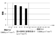
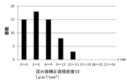
- the first threshold may be 15000 ⁇ m 3 / mm 2 .
- the second threshold may be 10 ⁇ m 3 / mm 2 .
- the calculating step may include a measuring step of measuring the depth of the depression at each position of the part of the surface.
- the measurement step may measure the depth of the depression by a laser microscope.
- the area of the part of the surface may be 0.1 mm 2 or more.
- One embodiment of the present disclosure is a metal plate for manufacturing a vapor deposition mask, wherein the metal plate has a plurality of depressions located on the surface of the metal plate, and a plurality of the metal plates are located on a part of the surface
- the depression correction volume is divided by the area of the part of the surface
- the depression correction volume density calculated by the following equation is 15000 ⁇ m 3 / mm 2 or less, and the depression correction volume is based on the result of measuring the depth of the depression at each position of the part of the surface by a laser microscope It is a metal plate which is calculated and whose said partial area of the said surface is 0.1 mm ⁇ 2 > or more.
- the hollow correction volume density may be 10 ⁇ m 3 / mm 2 or more.
- the metal plate may be made of an iron alloy containing nickel.
- One embodiment of the present disclosure is a method of manufacturing a deposition mask in which a plurality of through holes are formed, and preparing a metal plate manufactured by the method of manufacturing a metal plate described above, or the metal plate described above And a processing step of etching the metal plate to form the through hole in the metal plate.
- One embodiment of the present disclosure is a vapor deposition mask, comprising: a metal plate having a plurality of depressions positioned on a surface; and a plurality of through holes formed on the metal plate, the portion being located on a part of the surface
- the depression correction volume is the area of the part of the surface
- the depression correction volume density calculated by dividing is 15000 ⁇ m 3 / mm 2 or less, and the depression correction volume is a result of measuring the depth of the depression by each laser microscope at each position of the part of the surface. It is a vapor deposition mask which is calculated based on this, and the area of the said one part of the said surface is 0.1 mm ⁇ 2 > or more.
- the hollow correction volume density may be 10 ⁇ m 3 / mm 2 or more.
- a metal plate suitable for manufacturing a deposition mask can be efficiently obtained.
- FIG. 1 shows a deposition apparatus with a deposition mask apparatus according to an embodiment of the present disclosure. It is sectional drawing which shows the organic electroluminescence display (organic electroluminescence display intermediate body) manufactured using the vapor deposition mask apparatus shown in FIG. 1 is a plan view of a deposition mask apparatus according to an embodiment of the present disclosure.
- FIG. 4 is a partial plan view showing an effective area of the deposition mask shown in FIG. 3;
- FIG. 5 is a cross-sectional view taken along the line VV of FIG. 4;
- FIG. 6 is a cross-sectional view taken along the line VI-VI of FIG. 4;
- FIG. 7 is a cross-sectional view taken along the line VII-VII of FIG.
- FIG. 9 is a cross-sectional view taken along line IX-IX of FIG. 8; It is sectional drawing which expands and shows the through-hole and the area
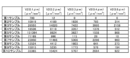
- FIG. 27 is a view showing a second surface etching step following FIG. 26; It is a figure which shows the process of removing resin and a resist pattern from a metal plate. It is a table
- a depression such as an oil pit may be formed on the surface of the rolled metal plate.
- the state of depressions on the surface of the metal plate affects the dimensional accuracy and positional accuracy of the through holes formed in the metal plate. For example, when the depth of the depression on the surface of the metal plate is increased, the size of the through hole formed in the metal plate is larger than the design value. Therefore, the technology to inspect the condition of the depression on the surface of the metal plate is important.
- Arithmetic mean roughness Ra refers to the position of the surface of the metal plate in the thickness direction in the thickness direction of the metal plate (hereinafter also referred to as height position) measured at a plurality of points on a predetermined straight line. It is a value obtained by calculating.
- the maximum height Ry is the difference between the maximum value and the minimum value of the measurement result when the height position of the surface of the metal plate is measured at a plurality of points on a predetermined straight line.
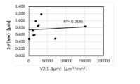
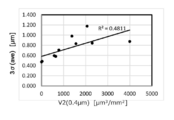
- the correlation between the surface roughness index in the prior art, such as arithmetic average roughness Ra, and the dimensional accuracy of the through hole formed in the metal plate is not necessarily high. I found out. For this reason, when judging the quality of a metal plate temporarily based on arithmetic mean coarseness Ra, in order to prevent an erroneous judgment, it is necessary to make a threshold of pass / fail judgment more severe than necessary. As a result, the yield of the metal plate is reduced.
- An embodiment of the present disclosure aims to provide a metal plate and a method of manufacturing the metal plate, a vapor deposition mask, and a method of manufacturing the vapor deposition mask that can effectively solve such problems.
- 1 to 28 are diagrams for describing an embodiment of the present disclosure.
- a method of manufacturing a deposition mask used to pattern an organic material on a substrate in a desired pattern when manufacturing an organic EL display device will be described as an example.
- embodiments of the present disclosure can be applied to a deposition mask used for various applications without being limited to such applications.
- plate is not distinguished from one another based only on the difference in designation.
- sheet is a concept including a member that may be called a sheet or a film.
- plate surface refers to a plate-shaped member (sheet-shaped member (sheet-shaped member) when the target plate-shaped (sheet-shaped, film-shaped) member is viewed globally and generally. It refers to the surface that coincides with the planar direction of the member (film-like member). Moreover, the normal direction used with respect to a plate-like (sheet-like, film-like) member refers to the normal direction to the plate face (sheet face, film face) of the member.
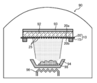
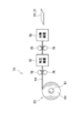
- the vapor deposition apparatus 90 may include a vapor deposition source (for example, a crucible 94), a heater 96, and a vapor deposition mask apparatus 10 therein. Further, the vapor deposition apparatus 90 may further include an exhaust unit for making the inside of the vapor deposition apparatus 90 a vacuum atmosphere.
- a vapor deposition source for example, a crucible 94
- the heater 96 heats the crucible 94 to evaporate the deposition material 98 under a vacuum atmosphere.
- the deposition mask device 10 is disposed to face the crucible 94.
- the deposition mask apparatus 10 may include a deposition mask 20 and a frame 15 for supporting the deposition mask 20.
- the frame 15 supports the deposition mask 20 in a state of being pulled in the surface direction so that the deposition mask 20 is not bent.
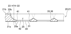
- the deposition mask apparatus 10 is disposed in the deposition apparatus 90 so that the deposition mask 20 faces a substrate, for example, an organic EL substrate 92, which is an object to which the deposition material 98 is to be attached.
- the face on the organic EL substrate 92 side is referred to as the first face 20a
- the face opposite to the first face 20a is referred to as the second face 20b.
- the vapor deposition mask apparatus 10 may be provided with the magnet 93 arrange
- the magnet 93 By providing the magnet 93, the vapor deposition mask 20 can be attracted to the magnet 93 side by magnetic force, and the vapor deposition mask 20 can be closely attached to the organic EL substrate 92.
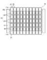
- FIG. 3 is a plan view showing the deposition mask device 10 as viewed from the first surface 20 a side of the deposition mask 20.
- the deposition mask apparatus 10 may include a plurality of deposition masks 20.
- Each vapor deposition mask 20 may include a pair of long sides 26 and a pair of short sides 27.
- each vapor deposition mask 20 may have a rectangular shape.
- Each vapor deposition mask 20 may be fixed to the frame 15 by spot welding, for example, at or near the pair of short sides 27.
- the vapor deposition mask 20 may include a metal plate-shaped substrate on which a plurality of through holes 25 penetrating the vapor deposition mask 20 are formed.
- the vapor deposition material 98 that has evaporated from the crucible 94 and reached the vapor deposition mask device 10 adheres to the organic EL substrate 92 through the through holes 25 of the vapor deposition mask 20.
- the deposition material 98 can be deposited on the surface of the organic EL substrate 92 in a desired pattern corresponding to the position of the through hole 25 of the deposition mask 20.
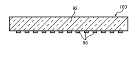
- FIG. 2 is a cross-sectional view showing an organic EL display device 100 manufactured using the vapor deposition apparatus 90 of FIG.
- the organic EL display device 100 at least includes an organic EL substrate 92 and a pixel including a vapor deposition material 98 provided in a pattern.
- the organic EL display device 100 further includes an electrode electrically connected to the pixel including the vapor deposition material 98.
- the electrodes are provided on the organic EL substrate 92 in advance, for example, before the deposition material 98 is attached to the organic EL substrate 92 by a deposition process.
- the organic EL display device 100 may further include other components such as a sealing member which seals a space around the pixel including the deposition material 98 from the outside. Therefore, it can be said that the organic EL display device 100 of FIG. 2 is an organic EL display device intermediate produced at an intermediate stage of manufacturing the organic EL display device.
- the vapor deposition apparatus 90 on which the vapor deposition mask 20 corresponding to each color is mounted is prepared, and the organic EL substrate 92 is sequentially put into each vapor deposition apparatus 90.
- the organic light emitting material for red, the organic light emitting material for green, and the organic light emitting material for blue can be sequentially deposited on the organic EL substrate 92.
- vapor deposition processing may be implemented inside the vapor deposition apparatus 90 used as a high temperature atmosphere.
- the deposition mask 20, the frame 15, and the organic EL substrate 92 held inside the deposition apparatus 90 are also heated during the deposition process.
- substrate 92 will show the behavior of the dimensional change based on each thermal expansion coefficient.
- frame 15 is a value equivalent to the thermal expansion coefficient of the organic electroluminescent board
- an iron alloy containing nickel can be used as a main material of the deposition mask 20 and the frame 15.
- an iron alloy containing 30% by mass or more and 54% by mass or less of nickel can be used as the material of the base material of the deposition mask 20.
- iron alloy containing nickel examples include an invar material containing 34 mass% or more and 38 mass% or less of nickel, a super invar material containing cobalt in addition to 30 mass% or more and 34 mass% or less of nickel, 38 Examples thereof include low thermal expansion Fe-Ni based plating alloys containing nickel in an amount of not less than 54% by mass.
- the thermal expansion coefficients of the deposition mask 20 and the frame 15 are the same as the thermal expansion coefficient of the organic EL substrate 92.
- a material other than the above-described iron alloy may be used as the material of the deposition mask 20.
- iron alloys other than iron alloys containing nickel described above, such as iron alloys containing chromium may be used.
- an iron alloy containing chromium for example, an iron alloy called a so-called stainless steel can be used.
- alloys other than iron alloys such as nickel and nickel-cobalt alloys may be used.
- the vapor deposition mask 20 includes a pair of ear parts (a first ear part 17 a and a second ear part 17 b) including a pair of short sides 27 of the vapor deposition mask 20 and a pair of ear parts 17 a and 17 b. And an intermediate portion 18 located therebetween.
- the ear portions 17 a and 17 b are portions of the deposition mask 20 fixed to the frame 15.
- the ear portions 17 a and 17 b are integrally formed with the intermediate portion 18.
- the ear portions 17a and 17b may be configured by members different from the intermediate portion 18. In this case, the ear portions 17a and 17b are joined to the intermediate portion 18 by welding, for example.
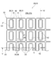
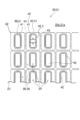
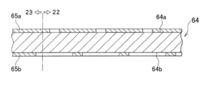
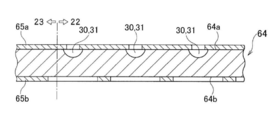
- the intermediate portion 18 may include at least one effective area 22 and a surrounding area 23 surrounding the effective area 22 in which the through holes 25 are formed from the first surface 20a to the second surface 20b.
- the effective area 22 is an area of the vapor deposition mask 20 facing the display area of the organic EL substrate 92.
- the intermediate portion 18 includes a plurality of effective regions 22 arranged at predetermined intervals along the long side 26 of the deposition mask 20.
- One effective area 22 corresponds to the display area of one organic EL display device 100.
- the vapor deposition mask device 10 shown in FIG. 1 multifaceted vapor deposition of the organic EL display device 100 is possible.
- one effective area 22 corresponds to a plurality of display areas.
- the effective area 22 may have, for example, a substantially rectangular shape in a plan view, and more specifically, a substantially rectangular outline in a plan view.
- each effective area 22 can have contours of various shapes according to the shape of the display area of the organic EL substrate 92.
- each effective area 22 may have a circular contour.
- each effective area 22 may have the same contour as the outer shape of a display device such as a smartphone.
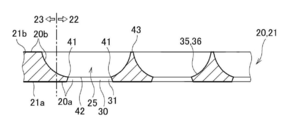
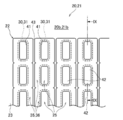
- FIG. 4 is an enlarged plan view of the effective area 22 from the second surface 20 b side of the vapor deposition mask 20.
- the plurality of through holes 25 formed in each effective area 22 are arranged at predetermined pitches along two directions orthogonal to each other in the effective area 22. May be An example of the through hole 25 will be further described in detail with reference mainly to FIGS. 5 to 7.
- 5 to 7 are cross-sectional views of the effective region 22 of FIG. 4 along the VV direction to the VII-VII direction, respectively.
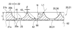
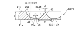
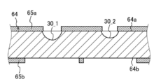
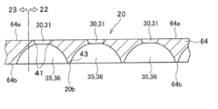
- the plurality of through holes 25 are along the normal direction N of the vapor deposition mask 20 from the first surface 20 a on one side along the normal direction N of the vapor deposition mask 20. It penetrates to the other side 20b.
- the first concave portion 30 is formed by etching in the first surface 21 a of the metal plate 21 on one side in the normal direction N of the deposition mask 20 as described in detail later.
- a second recess 35 is formed in the second surface 21 b of the metal plate 21 on the other side in the normal direction N.
- the first recess 30 is connected to the second recess 35 so that the second recess 35 and the first recess 30 communicate with each other.
- the through hole 25 is formed of a second recess 35 and a first recess 30 connected to the second recess 35.
- the plates of the vapor deposition mask 20 at respective positions along the normal direction N of the vapor deposition mask 20 from the side of the second surface 20 b of the vapor deposition mask 20 toward the side of the first surface 20 a The open area of each second recess 35 in the cross section along the surface gradually decreases.
- the opening area of each first recess 30 in the cross section along the plate surface of the vapor deposition mask 20 at each position along the normal direction N of the vapor deposition mask 20 is from the side of the first surface 20 a of the vapor deposition mask 20 It becomes smaller gradually toward the side of the second face 20b.
- connection portion 41 the wall surface 31 of the first recess 30 and the wall surface 36 of the second recess 35 are connected via the circumferential connection portion 41.
- the connection portion 41 the wall surface 31 of the first recess 30 inclined with respect to the normal direction N of the deposition mask 20 and the wall surface 36 of the second recess 35 inclined with respect to the normal direction N of the deposition mask 20 merge It is defined by the ridge line of the overhang.
- the connection portion 41 defines a through portion 42 in which the opening area of the through hole 25 is minimized in a plan view of the vapor deposition mask 20.
- two adjacent through holes 25 are deposited It is separated from each other along the plate surface of the mask 20. That is, in the case of manufacturing the first recess 30 by etching the metal plate 21 from the side of the first surface 21 a of the metal plate 21 corresponding to the first surface 20 a of the vapor deposition mask 20 as in the manufacturing method described later.
- the first surface 21 a of the metal plate 21 is left between the two adjacent first recesses 30.
- two adjacent second recesses 35 are spaced apart from one another along the surface of the deposition mask 20. That is, the second surface 21 b of the metal plate 21 remains between the two adjacent second recesses 35.
- a portion of the effective area 22 of the second surface 21 b of the metal plate 21 that is left without being etched is also referred to as a top portion 43.
- the deposition mask 20 be manufactured so that the width ⁇ of the top portion 43 does not become excessively large.
- the width ⁇ of the top portion 43 is preferably 2 ⁇ m or less.
- the width ⁇ of the top portion 43 changes in accordance with the direction in which the deposition mask 20 is cut.
- the widths ⁇ of the top portions 43 shown in FIGS. 5 to 7 may differ from one another.
- the vapor deposition mask 20 may be configured such that the width ⁇ of the top portion 43 is 2 ⁇ m or less even when the vapor deposition mask 20 is cut in any direction.
- the shadow is a phenomenon that adhesion of the deposition material to a region of the deposition object such as the organic EL substrate 92 overlapping the through hole of the deposition mask 20 is inhibited by the second surface 20 b or the wall surface of the deposition mask 20. It is.
- the first surface 20a of the vapor deposition mask 20 faces the organic EL substrate 92, as shown by a two-dot chain line in FIG.
- the second surface 20 b of the vapor deposition mask 20 is located on the side of the crucible 94 holding the vapor deposition material 98. Therefore, the vapor deposition material 98 passes through the second recess 35 whose opening area is gradually reduced and adheres to the organic EL substrate 92.
- the vapor deposition material 98 moves along the normal direction N of the organic EL substrate 92 from the crucible 94 toward the organic EL substrate 92 as indicated by an arrow from the second surface 20 b to the first surface 20 a in FIG. 5. Not only that, it may move in a direction greatly inclined with respect to the normal direction N of the organic EL substrate 92.
- the vapor deposition material 98 moving obliquely is easily caught on the top portion 43, the wall surface 36 of the second concave portion 35 and the wall surface 31 of the first concave portion 30.
- the proportion of vapor deposition material 98 that can not pass through 25 increases.
- the thickness t of the vapor deposition mask 20 can be reduced, thereby reducing the heights of the wall surface 36 of the second recess 35 and the wall surface 31 of the first recess 30. It is considered preferable. That is, it can be said that it is preferable to use, as the metal plate 21 for forming the vapor deposition mask 20, the metal plate 21 having a thickness t as small as possible within the range where the strength of the vapor deposition mask 20 can be secured. Taking this point into consideration, in the present embodiment, the thickness t of the vapor deposition mask 20 is, for example, 30 ⁇ m or less, preferably 25 ⁇ m or less, and more preferably 20 ⁇ m or less.
- the thickness t of the vapor deposition mask 20 may be 18 ⁇ m or less, or 15 ⁇ m or less.
- the thickness t of the vapor deposition mask 20 may be 5 ⁇ m or more, 7 ⁇ m or more, 10 ⁇ m or more, 13 ⁇ m or more, or 15 ⁇ m or more. May be
- the thickness t is the thickness of the peripheral region 23, that is, the thickness of the portion of the vapor deposition mask 20 where the first recess 30 and the second recess 35 are not formed. Therefore, the thickness t can also be said to be the thickness of the metal plate 21.
- the range of the thickness t of the vapor deposition mask 20 may be determined by a combination of any one of the plurality of upper limit candidate values described above and any one of the plurality of lower limit candidate values described above.
- the thickness t of the vapor deposition mask 20 may be 5 ⁇ m to 30 ⁇ m, may be 7 ⁇ m to 25 ⁇ m, may be 10 ⁇ m to 20 ⁇ m, and may be 13 ⁇ m to 18 ⁇ m.
- the range of the thickness t of the vapor deposition mask 20 may be determined by any two combination of the plurality of upper limit candidate values described above.
- the thickness t of the vapor deposition mask 20 may be 25 ⁇ m or more and 300 ⁇ m or less.
- the range of the thickness t of the vapor deposition mask 20 may be determined by any two of the plurality of lower limit candidate values described above.
- the thickness t of the vapor deposition mask 20 may be 5 ⁇ m or more and 7 ⁇ m or less.
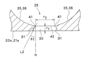
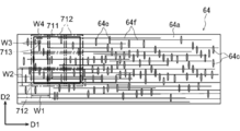
- a straight line L1 passing through the connection portion 41 which is the portion having the minimum opening area of the through hole 25 and any other position of the wall surface 36 of the second recess 35 is the normal direction of the vapor deposition mask 20.
- the minimum angle with respect to N is represented by the symbol ⁇ 1.
- a symbol ⁇ indicates the width of a portion (hereinafter, also referred to as a rib portion) remaining without being etched in the effective region 22 of the first surface 21 a of the metal plate 21.
- Dimension r 2 of the width ⁇ and the penetration portion 42 of the rib portion is determined as appropriate according to the size and number of display pixels of the organic EL display device.
- the width ⁇ of the rib portion is 5 ⁇ m or more and 40 ⁇ m or less
- the dimension r 2 of the through portion 42 is 10 ⁇ m or more and 60 ⁇ m or less.
- the width ⁇ of the rib portion may be 10 ⁇ m or more, 15 ⁇ m or more, or 20 ⁇ m or more.
- the width ⁇ of the rib portion may be 35 ⁇ m or less, 30 ⁇ m or less, or 25 ⁇ m or less.
- the range of the width ⁇ of the rib portion may be determined by any one of the plurality of upper limit candidate values described above and any one of the plurality of lower limit candidate values described above.
- the width ⁇ of the rib portion may be 10 ⁇ m to 35 ⁇ m, may be 15 ⁇ m to 30 ⁇ m, and may be 20 ⁇ m to 25 ⁇ m.
- the range of the width ⁇ of the rib portion may be determined by a combination of any two of the plurality of upper limit candidate values described above.
- the width ⁇ of the rib portion may be 35 ⁇ m or more and 40 ⁇ m or less.
- the range of the width ⁇ of the rib portion may be determined by a combination of any two of the plurality of lower limit candidate values described above.
- the width ⁇ of the rib portion may be 5 ⁇ m or more and 10 ⁇ m or less.
- the dimension r 2 of the penetrating portion 42 may be 15 ⁇ m or more, 20 ⁇ m or more, 25 ⁇ m or more, or 30 ⁇ m or more.
- the lower limit of the dimension r 2 of the penetrating portion 42 may be smaller than 10 ⁇ m above.
- the dimension r of the through portion 42 may be 5 ⁇ m or more.
- the dimension r 2 of the through portion 42 may be 55 ⁇ m or less, 50 ⁇ m or less, 45 ⁇ m or less, 40 ⁇ m or less, or 35 ⁇ m or less .
- any one of the candidate values of the plurality of upper limit mentioned may be defined by any one combination of the candidate value of the plurality of lower limit described above.
- the dimension r 2 of the penetrating portion 42 may be 15 ⁇ m to 55 ⁇ m, may be 20 ⁇ m to 50 ⁇ m, may be 25 ⁇ m to 45 ⁇ m, or may be 30 ⁇ m to 40 ⁇ m. And 30 ⁇ m or more and 35 ⁇ m or less.
- the range of dimensions r 2 of the penetrating portion 42 may be defined by any two combinations of the candidate values of the plurality of upper limit mentioned.
- the dimension r 2 of the through portion 42 may be 55 ⁇ m or more and 60 ⁇ m or less.
- the range of dimensions r 2 of the penetrating portion 42 may be defined by any two combinations of the candidate values of the plurality of lower limit described above.
- the dimension r 2 of the through portion 42 may be 5 ⁇ m or more and 10 ⁇ m or less.
- FIG. 9 is a cross-sectional view of the effective region 22 of FIG. 8 along the IX-IX direction.
- the vapor deposition mask 20 according to the present embodiment is particularly effective when producing an organic EL display device having a pixel density of 450 ppi or more.
- required in order to produce such a high pixel density organic electroluminescent display is demonstrated.
- FIG. 10 is an enlarged cross-sectional view of the through hole 25 of the vapor deposition mask 20 shown in FIG. 5 and a region in the vicinity thereof.
- FIG. 10 as a parameter related to the shape of through hole 25, the distance from first surface 20a of deposition mask 20 to connection portion 41 in the direction along normal direction N of deposition mask 20, ie, the first recess the height of the wall 31 of the 30 is represented by reference numeral r 1. Furthermore, the first recess 30 dimensions of the first recess 30 in the portion connected to the second recess 35, i.e. the dimension of the through region 42 is represented by reference numeral r 2. Further, in FIG. 10, an angle formed by a straight line L2 connecting the connection portion 41 and the tip end edge of the first recess 30 on the first surface 21a of the metal plate 21 with respect to the normal direction N of the metal plate 21 is It is represented by the symbol ⁇ 2.
- dimension r 2 of the penetrating part 42 is preferably set below and 60 ⁇ m or 10 [mu] m.
- the vapor deposition mask 20 which can produce the organic electroluminescence display of high pixel density can be provided.
- the height r 1 of the wall surface 31 of the first recess 30 is set to 6 ⁇ m or less.
- An angle ⁇ 2 can reach the organic EL substrate 92 among the deposition materials 98 that are inclined with respect to the normal direction N of the metal plate 21 and pass through the through portion 42 near the connection portion 41. This corresponds to the maximum value of the inclination angle of the material 98. This is because the vapor deposition material 98 flying through the connecting portion 41 at an inclination angle larger than the angle ⁇ 2 adheres to the wall surface 31 of the first recess 30 before reaching the organic EL substrate 92.
- the angle ⁇ 2 it is possible to suppress the deposition material 98 flying at a large inclination angle and passing through the penetrating portion 42 from adhering to the organic EL substrate 92, whereby the organic EL substrate 92 It can suppress that the vapor deposition material 98 adheres to the part more outer than the part which overlaps with the penetration part 42 among them. That is, reducing the angle ⁇ 2 leads to suppression of the variation in the area and thickness of the vapor deposition material 98 attached to the organic EL substrate 92. From such a viewpoint, for example, the through hole 25 is formed such that the angle ⁇ 2 is 45 degrees or less. In FIG.
- the dimension of the first recess 30 in the first surface 21a is larger than the dimension r2 of the first recess 30 in the connection portion 41.
- An example is shown. That is, an example is shown in which the value of the angle ⁇ 2 is a positive value.
- the dimension r2 of the first recess 30 in the connection portion 41 may be larger than the dimension of the first recess 30 in the first surface 21a. That is, the value of the angle ⁇ 2 may be a negative value.
- the metal plate used to manufacture a deposition mask.
- the metal plate is made of a rolled material of an iron alloy containing nickel.
- the rolled material may have a thickness of 30 ⁇ m or less.
- the rolled material may also contain 30% by mass or more and 38% by mass or less of nickel, 0% by mass or more and 6% by mass or less of cobalt, the balance of iron, and unavoidable impurities.
- each raw material is prepared such that the ratio of iron to the total raw material and the ratio of nickel are about 64% by weight and about 36% by weight, respectively.
- each raw material is pulverized if necessary, and then a melting step of melting each raw material in a melting furnace is performed.
- the raw materials are melted and mixed using a gas discharge such as an arc discharge.
- the temperature at the time of melting is set according to the raw material, and is, for example, 1500 ° C. or more.
- the melting step may include a step of charging aluminum, manganese, silicon or the like into a melting furnace for deoxidation, dehydration, denitrification and the like.
- the melting step may be performed under an atmosphere of an inert gas such as argon gas at a low pressure state lower than atmospheric pressure.
- a grinding process may be performed to remove the surface of the base material. This allows the removal of oxide coatings such as scale.
- the specific grinding method is not particularly limited, the so-called grinding method of rotating the grinding wheel to cut the surface of the base material, or the so-called pushing method of pushing the base material into a cutting tool to cut the surface of the base material Etc. can be adopted.
- the grinding process may be performed to make the thickness of the base material uniform.
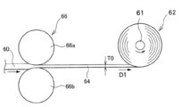
- the rolling process of rolling the base material 60 comprised from the iron alloy containing nickel is implemented.
- the sheet is conveyed toward the rolling device 66 including the pair of rolling rolls 66a and 66b (work rolls) while applying tensile tension in the direction indicated by the arrow D1.
- the base material 60 reached between the pair of rolling rolls 66a and 66b is rolled by the pair of rolling rolls 66a and 66b.
- the thickness of the base material 60 is reduced and the base material 60 is stretched along the transport direction.
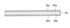
- the metal plate 64 of thickness T0 can be obtained.
- the wound body 62 may be formed by winding the metal plate 64 around the core 61.
- FIG. 11 merely shows an outline of the rolling process, and the specific configuration and procedure for carrying out the rolling process are not particularly limited.
- a hot rolling process of processing the base material at a temperature higher than the temperature changing the crystal arrangement of the iron alloy constituting the base material 60 or a base material at a temperature lower than the temperature changing the crystal arrangement May include a cold rolling step of processing
- the direction in which the base material 60 and the metal plate 64 are passed between the pair of rolling rolls 66a and 66b is not limited to one direction.
- FIG. 11 and FIG. 12 by repeatedly passing the base material 60 and the metal plate 64 between the pair of rolling rolls 66a and 66b in the direction from left to right in the drawing and from right to left in the drawing
- the base material 60 and the metal plate 64 may be rolled gradually.
- the surface roughness of the metal plate 64 can be adjusted by adjusting the diameters of the rolling rolls 66a and 66b in contact with the base material 60. For example, by reducing the diameter of the rolling rolls 66a and 66b, the volume of a recess, which will be described later, present on the surface of the metal plate 64 can be reduced. Thereby, for example, the hollow correction volume density to be described later can be set to 15000 ⁇ m 3 / mm 2 or less.
- the diameter of the rolling rolls is preferably 28 mm or more.
- the diameter of the rolling roll may be 40 mm or more, and may be 50 mm or more.
- the diameter of the rolling roll is preferably 150 mm or less.
- the diameter of the rolling roll may be 120 mm or less, 100 mm, or 80 mm or less.
- the range of the diameter of the rolling roll may be defined by any one of a plurality of upper limit candidate values and a combination of any one of a plurality of lower limit candidate values.
- the diameter of the rolling roll may be 28 mm or more and 150 mm or less, or 40 mm or more and 120 mm or less.
- the range of the diameter of the rolling roll may be defined by any two of the plurality of upper limit candidate values.
- the diameter of the rolling roll may be 120 mm or more and 150 mm or less.
- the range of the diameter of the rolling roll may be defined by any two of the plurality of lower limit candidate values.
- the diameter of the rolling roll may be 28 mm or more and 40 mm or less.
- the diameter of the rolling roll is preferably 28 mm or more and 150 mm or less, more preferably 40 mm or more and 120 mm or less, more preferably 50 mm or more and 100 mm or less, and more preferably 50 mm or more and 80 mm or less.
- the pressure of the rolling actuator may be adjusted.
- the shape of the backup roll may be appropriately adjusted in addition to the rolling rolls (work rolls) 66a and 66b, and the position of the backup roll may be appropriately adjusted in the sheet width direction.
- the rolling speed that is, the transfer speed of the base material may be adjusted. From the viewpoint of further reducing the hollow correction volume density, it is preferable to reduce the rolling speed.
- By reducing the rolling speed it is possible to reduce the amount of coolant, such as rolling oil, which is caught between the base material 60 and the rolling rolls 66a, 66b. Thereby, the number, area, etc. of the oil pits formed on the surface of the metal plate 64 can be reduced.
- the rolling speed is preferably 30 m / min or more.
- the rolling speed may be 50 m / min or more, 70 m / min or more, or 100 m / min or more.
- the rolling speed is preferably 200 m / min or less.
- the rolling speed may be 150 m / min or less, 100 m / min or less, or 80 m / min or less.
- the rolling speed may be determined by a combination of any one of a plurality of upper limit candidate values and any one of a plurality of lower limit candidate values.
- the rolling speed may be 30 m / min or more and 200 m / min or less, and may be 50 m / min or more and 150 m / min or less.
- the range of the rolling speed may be defined by any two combination of a plurality of upper limit candidate values.
- the rolling speed may be 150 m / min or more and 200 m / min or less, and may be 100 m / min or more and 150 m / min or less.
- the range of the rolling speed may be defined by any two combination of a plurality of lower limit candidate values.
- the range of the rolling speed may be 30 m / min or more and 50 m / min or less, and may be 50 m / min or more and 70 m / min or less.
- the rolling speed is preferably 30 m / min to 200 m / min, more preferably 30 m / min to 150 m / min, and more preferably 30 m / min to 100 m / min, more preferably 30 m / min. Min to 80 m / min.
- a coolant such as kerosene or neat oil may be supplied between the base material 60 and the rolling rolls 66a and 66b. Thereby, the temperature of the base material can be controlled. From the viewpoint of reducing the depression correction volume density, it is preferable to reduce the coolant supply amount.
- the number and area of oil pits and rolling streaks formed on the surface of the metal plate 64 can also be adjusted by appropriately selecting the coolant.
- neat oil can be used as the coolant. Neat oil has a characteristic that an increase in viscosity during rolling hardly occurs. Therefore, by using neat oil as the coolant, it is possible to reduce the amount of coolant which is caught between the base material 60 and the rolling rolls 66a and 66b. Thus, the formation of oil pits on the surface of the metal plate 64 can be suppressed.
- the number of oil pits and rolling streaks formed on the surface of the metal plate 64 can be adjusted. For example, by reducing the surface roughness Ra of the rolling rolls, formation of rolling streaks on the surface of the metal plate 64 can be suppressed.
- the surface roughness Ra of the rolling roll is preferably 0.2 ⁇ m or less.
- the surface roughness Ra of the rolling roll may be 0.15 ⁇ m or less, 0.1 ⁇ m or less, or 0.05 ⁇ m or less.
- the surface roughness Rz of the rolling roll is preferably 2.0 ⁇ m or less.
- the surface roughness Rx of the rolling roll may be 1.5 ⁇ m or less, 1.0 ⁇ m or less, or 0.5 ⁇ m or less.
- the surface roughness Rz of the rolling roll is preferably 2.0 ⁇ m or less.
- the surface roughness Rz of the rolling roll may be 1.5 ⁇ m or less, may be 1.0 ⁇ m or less, and may be 0.5 ⁇ m or less.
- Surface roughness Ra and Rz are measured based on JIS B 0601: 2013.
- the analysis process which analyzes the quality and the characteristic of the base material 60 or the metal plate 64 before and after a rolling process, or between a rolling process.
- the composition may be analyzed by irradiating the base material 60 or the metal plate 64 with fluorescent X-rays.
- the amount of thermal expansion of the base material 60 or the metal plate 64 may be measured by thermomechanical analysis (TMA).
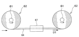
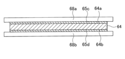
- an annealing step of annealing the metal plate 64 using an annealing apparatus 67 may be performed as shown in FIG.
- the annealing step may be performed while pulling the metal plate 64 in the transport direction (longitudinal direction), as shown in FIG. That is, the annealing step may be performed as continuous annealing while being transported, not so-called batch annealing. In this case, it is preferable to set the temperature and the transport speed so as to suppress the occurrence of deformation such as buckling in the metal plate 64.
- the annealing step it is possible to obtain the metal plate 64 from which the residual strain has been removed to some extent.
- FIG. 12 the example which conveys the metal plate 64 in the horizontal direction at the time of an annealing process is shown in FIG. 12, it is not restricted to this, the metal plate 64 at the time of an annealing process, It may be transported in other directions.
- the conditions of the annealing step are appropriately set according to the thickness of the metal plate 64, the rolling reduction, etc.
- the annealing step is performed within a range of 500 ° C. to 600 ° C. for 30 seconds to 90 seconds. Ru.
- the above-mentioned number of seconds represents the time required for the metal plate 64 to pass through the space adjusted to a predetermined temperature in the annealing device 67.
- the temperature of the annealing step may be set so as not to cause the softening of the metal plate 64.
- the lower limit of the temperature of the annealing step may be lower than 500 ° C. described above.
- the temperature of the annealing step may be 400 ° C. or higher, and may be 450 ° C. or higher.
- the upper limit of the temperature of the annealing step may be higher than the above-described 600 ° C.
- the temperature of the annealing step may be 700 ° C. or less, or 650 ° C. or less.
- the range of the temperature of the annealing step may be determined by any one of the plurality of upper limit candidate values described above and any one of the plurality of lower limit candidate values described above.
- the temperature of the annealing step may be 400 ° C.
- the range of the temperature of the annealing step may be determined by any two of the plurality of upper limit candidate values described above.
- the temperature of the annealing step may be 650 ° C. or more and 700 ° C. or less.
- the range of the temperature of the annealing step may be determined by a combination of any two of the plurality of lower limit candidate values described above.
- the temperature of the annealing step may be 400 ° C. or more and 450 ° C. or less.
- the time of the annealing step may be 40 seconds or more or 50 seconds or more. Further, the lower limit of the time of the annealing step may be shorter than the above-mentioned 30 seconds. For example, the time of the annealing step may be 10 seconds or more, or 20 seconds or more. In addition, the time of the annealing step may be 80 seconds or less, 70 seconds or less, or 60 seconds or less. In addition, the upper limit of the annealing process time may be longer than the above-described 90 seconds. For example, the annealing process time may be 100 seconds or less.
- the range of time of the annealing step may be determined by any one of the plurality of upper limit candidate values described above and any one of the plurality of lower limit candidate values described above.
- the time of the annealing step may be 10 seconds to 100 seconds, may be 20 seconds to 90 seconds, may be 30 seconds to 80 seconds, and is 40 seconds to 70 seconds. It may be 50 seconds or more and 60 seconds or less.
- the time range of the annealing step may be defined by any two combination of the plurality of upper limit candidate values described above.
- the time of the annealing process may be 90 seconds or more and 100 seconds or less.
- the time range of the annealing step may be defined by any two of the plurality of lower limit candidate values described above.
- the time of the annealing step may be 10 seconds or more and 20 seconds or less.
- the annealing step described above is performed in a non-reducing atmosphere or an inert gas atmosphere.
- the non-reducing atmosphere is an atmosphere containing no reducing gas such as hydrogen.
- Does not contain reducing gas means that the concentration of reducing gas such as hydrogen is 10% or less.
- the concentration of the reducing gas may be 8% or less, 6% or less, 4% or less, or 2% or less, or 1% or less It may be
- the inert gas atmosphere is an atmosphere in which the concentration of inert gas such as argon gas, helium gas, nitrogen gas, etc. is 90% or more.
- the concentration of the inert gas may be 92% or more, 94% or more, 96% or more, 98% or more, or 99% or more. It may be By performing the annealing step in a non-reducing atmosphere or an inert gas atmosphere, it is possible to suppress the formation of a nickel compound such as nickel hydroxide in the surface layer of the metal plate 64.
- the annealing apparatus 67 may have a mechanism for monitoring the concentration of the inert gas or a mechanism for adjusting the concentration of the inert gas.
- a cleaning step of cleaning the metal plate 64 may be performed before the annealing step. Thereby, the adhesion of foreign matter to the surface of the metal plate 64 can be suppressed in the annealing step.
- a cleaning solution for cleaning for example, a hydrocarbon-based solution can be used.
- the invention is not limited thereto, and the metal plate 64 is wound around the core 61 in the annealing process. It may be carried out in the That is, batch annealing may be performed.
- the annealing step is performed in a state where the metal plate 64 is wound around the core 61, the metal plate 64 may have a wrinkle of warpage corresponding to the winding diameter of the wound body 62. Therefore, depending on the winding diameter of the winding body 62 and the material constituting the base material 60, it is advantageous to carry out the annealing step while pulling the metal plate 64 in the longitudinal direction.
- a slitting process may be performed to cut off both ends in the width direction of the metal plate 64 obtained by the rolling process so that the width of the metal plate 64 is within the predetermined range.
- This slitting process is performed to remove cracks that may occur at both ends of the metal plate 64 due to rolling. By carrying out such a slitting process, it is possible to prevent the phenomenon that the metal plate 64 is broken, so-called plate breakage, from being generated from a crack as a starting point.
- the width of the portion to be cut off in the slit process may be adjusted so that the shape of the metal plate 64 after the slit process is symmetrical in the width direction. Also, the slitting process may be performed before the above-mentioned annealing process.
- an appearance inspection process of inspecting the appearance of the metal plate 64 may be performed.
- the appearance inspection step may include the step of inspecting the appearance of the metal plate 64 using an automatic inspection machine. Further, the appearance inspection step may include a step of inspecting the appearance of the metal plate 64 visually.
- a shape inspection process may be performed to inspect the shape of the metal plate 64.
- the position of the surface of the metal plate 64 in the thickness direction may be measured within a predetermined region of the metal plate 64 using a three-dimensional measuring device.
- FIG. 13 is a view showing how a plurality of depressions 64 c exist, for example, on the first surface 64 a on the surface of the metal plate 64 obtained by rolling.
- the depression 64 c is, for example, an oil pit 64 e or a rolling streak 64 f.
- the oil pit 64e is a recess formed on the surface of the metal plate 64 due to the oil present between the base material 60 and the rolling rolls 66a and 66b.
- the recess 64 c means a recess having a depth of 0.2 ⁇ m or more among recesses such as oil pits 64 e present on the surface of the metal plate 64.
- the density of the depressions 64 c present on the surface of the metal plate 64 is, for example, 3 pieces / mm 2 or more and 500 pieces / mm 2 or less.
- the numerical value 0.2 ⁇ m is a preferable value of the correction distance dC described later.
- the dimension of the hollow 64c in the surface direction of the metal plate 64 is, for example, 1 ⁇ m or more and 60 ⁇ m or less.
- a technique for calculating the arithmetic mean roughness Ra and the maximum height Ry of the surface is known.
- the position of the surface of the metal plate 64 in the thickness direction is measured at a plurality of points on a predetermined straight line such as a straight line R1 or a straight line R2 shown in FIG. 13 in any of the arithmetic average roughness Ra and the maximum height Ry.
- the density of the depressions 64c may vary depending on the place. As a result, as shown in FIG.
- the density of the depressions 64c located on the straight line R2 can be significantly lower than the density of the depressions 64c located on the straight line R1.
- the variation in inspection results may be relatively large.
- FIG. 14 is a view showing an example of the cross section of the metal plate 64. As shown in FIG.
- the recess 64c_1 located on the left side and the recess 64c_2 located in the center have the same aperture diameter A.
- the wall surface of the recess 64c_1 has a shape that is convex toward the metal plate.
- the wall surface of the recess 64c_2 has a shape which is convex outward as opposed to the recess 64c_1.
- the two recesses 64c_3 located on the right side have an aperture diameter A / 2. That is, the sum of the opening diameters of the two depressions 64c_3 is the same as the opening diameter of the depression 64c_1 and the opening diameter of the depression 64c_2.
- the depths of the three types of depressions 64c_1, 64c_2 and 64c_3 are all B.
- the influence which three types of hollows 64c_1, 64c_2, 64c_3 have on the measured value of arithmetic mean roughness Ra is the same.
- the surface roughness is evaluated based on the volume of the recess.
- the degree of influence of the three types of depressions 64c_1, 64c_2 and 64c_3 on the depression correction volume density to be described later is different. Specifically, the degree of influence of the depression 64c_1 on the depression correction volume density is maximized. Further, the degree of influence of one depression 64c_2 on the depression correction volume density is smaller than the degree of influence of two depressions 64c_3 on the depression correction volume density.
- FIG. 15 is a cross-sectional view showing a step of forming the first recess 30 by etching the metal plate 64 shown in FIG. 14 from the first surface 64a side using the first resist pattern 65a as a mask.
- the volume of the left recess 64c_1 is larger than the volume of the right recess 64c_2. Therefore, in the place where the recess 64c_1 on the left side is present, the etching progresses in the thickness direction and the surface direction of the metal plate 64 more quickly than the place where the recess 64c_2 on the right side exists. Therefore, the dimension of the first recess 30_1 formed in the place where the recess 64c_1 on the left side is larger than the dimension of the first recess 30_2 formed in the place where the recess 64c_2 on the right side exists.
- FIG. 17 is a diagram for explaining how the accuracy of the opening dimension of the through hole 25 on the first surface 20 a side is reduced due to the recess 64 c of the metal plate 64.
- the etching solution can infiltrate into the depression 64c at the start of the etching process. Therefore, in the portion where the large-volume depression 64 c is present, the etching can progress in the thickness direction and the surface direction of the metal plate 64 earlier than the other portions. Therefore, for example, when a large hollow 64c exists near the end of the opening of the first resist pattern 65a or near the end of the opening of the second resist pattern 65b in the metal plate 64, the hollow 64c is formed.
- the dimension of the through hole 25 in the surface direction of the metal plate 64 may be increased in the portion where there were.
- the variation of the dimension r 3 on the first surface 20a of the first recess 30 constituting the through hole 25 in the place where the large volume of the recess 64c exists. Can occur.
- Such variation in the opening dimension may also occur in the second recess 35 on the second surface 20 b side.
- the through holes 25 can be precisely formed in the metal plate 64 largely depends not only on the depth of the depression 64 c formed on the surface of the metal plate 64 but also on the volume of the depression 64 c. .
- the technique based on the conventional arithmetic mean roughness Ra etc. can not acquire appropriately the information regarding the volume of hollow 64c. For this reason, when inspecting the metal plate 64 using the arithmetic average roughness Ra, in order to prevent the metal plate 64 unsuitable for manufacturing the deposition mask 20 from passing the inspection, the threshold value of the pass / fail judgment is necessary or more Need to be strict. As a result, it is considered that the yield of the metal plate 64 is reduced.
- the inspection of the metal plate 64 be performed in consideration of the volume of the recess 64 c.
- the degree of the reduction in the dimensional accuracy of the through holes 25 of the vapor deposition mask 20 caused by the depressions 64 c can be predicted more accurately.
- the metal plate 64 can be inspected without making the threshold of the pass / fail judgment more severe than necessary, and the yield of the metal plate 64 can be increased.
- an example of the inspection process in consideration of the volume of the recess 64 c will be described with reference to FIGS. 18 and 19.
- FIG. 18 is a plan view showing a part of the first surface 64 a of the metal plate 64 in an enlarged manner. A plurality of depressions 64c are formed in the first surface 64a.
- the code D1 represents the transport direction (hereinafter also referred to as the first direction) of the metal plate 64 in the rolling process. Further, a code D2 represents a direction (hereinafter, also referred to as a second direction) orthogonal to the first direction D1.
- the quality of the metal plate 64 is determined based on the volumes of the plurality of depressions 64 c located in the inspection area 711 of the first surface 64 a shown in FIG. 18.
- the area U1 of the inspection area 711 is, for example, 0.1 mm 2 or more and 1.5 mm 2 or less.
- the inspection process has a calculation process S1 and a determination process S2.
- a hollow correction volume density is calculated.
- the depression correction volume density is an index having a high correlation with the dimensional accuracy of the components of the deposition mask 20, as supported in the examples described later.
- the metal plate 64 is determined to be good when the depression correction volume density is equal to or less than a predetermined threshold.
- the calculation step S1 includes a measurement step S11 and a processing step S12.
- imaging is performed in each of the plurality of unit areas 712, and the depth of the recess 64c is measured from the obtained image.
- the unit area 712 is, for example, a rectangular area having a side with a length W1 and a side with a length W2, as shown in FIG.
- the unit area 712 corresponds to the range of images that can be acquired in one shooting.
- the side of the length W1 is parallel to the first direction D1
- the side of the length W2 is parallel to the second direction D2.
- W1 is 270 ⁇ m and W2 is 202 ⁇ m.
- the side of the length W1 is parallel to the first direction D1 means that the angle formed by the side of the length W1 and the first direction D1 is in the range of ⁇ 10 ° to + 10 °.
- the side of the length W2 is parallel to the second direction D2 means that the angle formed by the side of the length W2 and the second direction D2 is in the range of -10 ° to + 10 °.
- two or more unit areas 712 adjacent in the first direction D1 partially overlap each other, and two unit areas 712 adjacent in the second direction D2 partially overlap also in the plurality of times of imaging. It will be implemented.
- image connection software or the like By connecting a plurality of images obtained by this using image connection software or the like, it is possible to obtain an image of an area larger than one unit area 712.
- a region indicated by reference numeral 711 in FIG. 18 is extracted as an inspection region from the images obtained by linking.
- the inspection area 711 is defined so as to surround one unit area 712 located at the center among the nine unit areas 712 shown in FIG. 18 and to partially include each of the eight unit areas 712 located at the periphery.
- the length of the inspection area 711 in the first direction D1 is, for example, 700 ⁇ m
- the length of the inspection area 711 in the second direction D2 is, for example, 500 ⁇ m.
- symbol 713 shows the pixel corresponded to the resolution of a test
- One pixel 713 corresponds to, for example, one spot of a laser that the inspection device irradiates the metal plate 64.
- the length W3 and the length W4 of the pixel 713 in the first direction D1 and the second direction D2 are preferably 0.1 ⁇ m or more and 0.4 ⁇ m or less.
- the area U2 of the pixel 713 is preferably 0.01 ⁇ m 2 or more and 0.2 ⁇ m 2 or less.
- the length of the pixel 713 in the first direction D1 and the second direction D2 are 0.263 ⁇ m.
- the area U2 of the pixel 713 is 0.069 ⁇ m 2 .
- FIG. 19 is a cross-sectional view showing a case where the metal plate 64 in which the depression 64 c is formed is cut in parallel to the first direction D1.
- the symbol d (k) represents the distance from the first surface 64a to the bottom surface of the recess 64c in the pixel 713 located at the coordinate x (k) in the first direction D1.
- k is an integer, and the range that k can take is determined by the resolution of the image.
- the measurement result of the depth of the recess 64c may vary due to the state of the first surface 64a around the recess 64c.
- the position of the reference plane RP which is a virtual plane, may be adopted as the position of the first surface 64a in the thickness direction of the metal plate 64. .
- the reference surface RP will be described below.
- the reference plane RP of the first plane 64a is, for example, a plane estimated by the method of least squares. Specifically, first, the position of the inspection area 711 in the thickness direction of the surface of the first surface 64 a of the metal plate 64 is measured using a laser microscope described later. Subsequently, a predetermined plane is temporarily set as the reference plane RP, and the square of the distance from the position of the surface of the first plane 64a to the reference plane RP is calculated in each pixel 713. In this case, a plane in which the sum of squares of distances is minimized can be adopted as the reference plane RP.
- the depth d (k) of the depression 64c is measured in each pixel 713 of the inspection area 711.
- the measurement value of the depth is a value of the distance from the measurement value of the position in the thickness direction of the surface of the first surface 64 a of the metal plate 64 to the reference surface RP estimated by the least square method.
- a laser microscope can be used, for example.
- the inspection area 711 of the first surface 64 a of the metal plate 64 is irradiated with a laser beam.
- the laser beam reflected by the inspection area 711 is photographed as a two-dimensional reflection image of the inspection area 711 using an image sensor or the like of a CCD or CMOS.
- the two-dimensional reflection image is analyzed based on the principle of the confocal microscope to measure the position of each pixel 713 in the inspection area 711 in the thickness direction of the surface of the first surface 64 a of the metal plate 64.
- a laser microscope for example, a laser microscope VK-X200 series manufactured by Keyence Corporation can be used.
- step S12 based on the depth of the depression 64c measured in each pixel 713 in the inspection area 711, information on the volume of the depression 64c in the inspection area 711 is calculated.
- a correction surface CP located on the second surface 64 b side by a predetermined correction distance dC from the reference surface RP in the thickness direction of the metal plate 64 is set.
- the sum of the volumes of portions of the depressions 64c located in the inspection area 711 located on the second surface 64b side with respect to the correction distance dC in the thickness direction of the metal plate 64 is calculated.
- a value d (k) -dC is calculated by subtracting the correction distance dC from the depth d (k) for a portion having a depth greater than the correction distance dC in the depression 64c located in the inspection area 711.
- the value d (k) -dC is multiplied by the area U2 of the pixel 713.
- the respective volumes V (k) are integrated over the entire area of the inspection area 711. Thereby, the sum of the volumes of portions of the depressions 64c located in the inspection area 711 located closer to the second surface 64b than the correction surface CP. (Hereinafter, also referred to as depression correction volume) V1 can be calculated.
- the depression correction volume V1 is divided by the area U1 of the inspection area 711. By this, it is possible to calculate the depression correction volume per unit area (hereinafter also referred to as depression correction volume density) V2.
- the above-mentioned correction distance dC is preferably 0.1 ⁇ m or more and 0.5 ⁇ m or less, and is, for example, 0.2 ⁇ m.
- the depression correction volume V1 and the depression correction volume density V2 obtained when the correction distance dC is set to z ⁇ m are respectively the depression correction volume V1 (z ⁇ m) and the depression correction volume density V2 (z ⁇ m)
- the expressions “depression correction volume V1 (0.2 ⁇ m) and depression correction volume density V2 (0.2 ⁇ m)” may be adopted.
- a determination step S2 of determining the metal plate 64 as good is performed. Thereby, the metal plate 64 which can form accurately the component of the vapor deposition mask 20, such as the through hole 25, can be sorted out.
- the threshold TH1 is appropriately determined based on the dimensional accuracy required for the components of the vapor deposition mask 20, the setting of the correction distance dC, and the like. For example, it is required that the error of the opening dimension of the through hole 25 of the vapor deposition mask 20, such as r 3 of the first recess 30 or the dimension r 2 of the through portion 42 described above, be ⁇ 1.0 ⁇ m or less, and When dC is 0.2 ⁇ m, the threshold TH1 can be set to 15000 ⁇ m 3 / mm 2 .
- Threshold TH1 may be a 12000 ⁇ m 3 / mm 2, may be a 10000 3 / mm 2 may be a 9000 ⁇ m 3 / mm 2, it may be a 6000 ⁇ m 3 / mm 2, 5000 ⁇ m 3 / mm may be 2, may be a 3000 .mu.m 3 / mm 2, may be a 1000 .mu.m 3 / mm 2.
- the determination step S2 may determine that the metal plate 64 is good when the depression correction volume density V2 is equal to or greater than the threshold TH2 and equal to or less than the threshold TH1. That is, in addition to the threshold TH1 that defines the upper limit of the depression correction volume density V2, the determination step S2 may use the threshold TH2 that defines the lower limit of the depression correction volume density V2.
- the adhesion of the resist film to the surface of the metal plate 64 can be enhanced by the metal plate 64 having the depression correction volume density V2 of the threshold TH2 or more.
- the upper threshold TH1 may be referred to as a first threshold
- the lower threshold TH2 may be referred to as a second threshold.
- the threshold TH2 may be 10 ⁇ m 3 / mm 2 , may be 100 ⁇ m 3 / mm 2 , may be 500 ⁇ m 3 / mm 2 , or may be 1000 ⁇ m 3 / mm 2 , or 3000 ⁇ m 3.
- / mm may be 2, may be a 4000 .mu.m 3 / mm 2, may be a 5000 .mu.m 3 / mm 2.
- the range of the depression correction volume density V2 of the metal plate 64 determined as good in the determination step S2 is any one of the plurality of upper limit threshold TH1 candidates and the plurality of lower limit thresholds TH2 described above. It may be determined by a combination of any one of the candidates. For example, a metal plate 64 which is determined as good, i.e.
- the recess corrected volumetric density V2 has a metal plate 64 which is selected, may also be 10 [mu] m 3 / mm 2 or more 15000 ⁇ m 3 / mm 2 or less, 100 [mu] m 3 / mm 2 more 12000 ⁇ m 3 / mm 2 may be less, 500 [mu] m 3 / mm 2 or more 10000 3 / mm 2 may be less, it may also be 1000 ⁇ m 3 / mm 2 or more 9000 ⁇ m 3 / mm 2 or less, 3000 .mu.m 3 / mm 2 or more 6000 ⁇ m 3 / mm 2 may be less or may be 4000 ⁇ m 3 / mm 2 or more 6000 ⁇ m 3 / mm 2 or less.
- the range of the depression correction volume density V2 that the sorted metal plate 64 has may be determined by a combination of any two of the above-described plurality of upper limit threshold TH1 candidates.
- the depression correction volume density V2 of the sorted metal plate 64 may be 12000 ⁇ m 3 / mm 2 or more and 15000 ⁇ m 3 / mm 2 or less.
- the range of the depression correction volume density V2 of the sorted metal plate 64 may be determined by a combination of any two of the plurality of lower limit threshold TH2 candidates.
- the depression correction volume density V2 of the sorted metal plate 64 may be 10 ⁇ m 3 / mm 2 or more and 100 ⁇ m 3 / mm 2 or less.
- FIG. 39 is a view showing an example of the distribution of the depression correction volume density V2 of the plurality of metal plates 64 sorted based on the determination condition of determining the metal plate having the depression correction volume density V2 equal to or less than the threshold TH1 as a non-defective product. is there.
- the horizontal axis represents the value of the depression correction volume density V2 calculated for each metal plate 64.
- the vertical axis indicates the number of metal plates 64 having the hollow correction volume density V2 in the range indicated by the horizontal axis. For example, among the plurality of metal plates 64 which are selected, the number of the metal plate 64 having a 6000 ⁇ m 3 / mm 2 or more 9000 ⁇ m 3 / mm 2 less than recess correction bulk density V2 is 17.
- the threshold TH1 is 15000 ⁇ m 3 / mm 2 .
- most of the metal plates 64 determined as non-defective products, for example, 95% or more have a depression correction volume density V2 of 15000 ⁇ m 3 / mm 2 or less.
- a part of the sorted metal plate 64 has a depression correction volume density V2 exceeding 15000 ⁇ m 3 / mm 2 due to a measurement error or the like.
- FIG. 40 shows an example of the distribution of the hollow correction volume density V2 of the plurality of metal plates 64 sorted based on the determination condition of determining the metal plate whose hollow correction volume density V2 is not less than the threshold TH2 and not more than the threshold TH1 as a good product.
- FIG. The meanings of the horizontal and vertical axes shown in FIG. 40 are the same as in the case of FIG.
- the threshold TH2 is 3000 ⁇ m 3 / mm 2
- the threshold TH1 is 15000 ⁇ m 3 / mm 2.
- the range of the metal plate 64 selected as the non-defective product is narrower than that of the example of FIG. In this case, when the sorting shown in FIG. 40 is performed, the sorting shown in FIG. 39 is also performed.
- an inspection step of inspecting the metal plate 64 based on the depression correction volume density V2 is used to determine the quality of the metal plate 64, that is, to sort the metal plate 64.
- the inspection step functions as a sorting step of sorting the metal plate 64 in the method of manufacturing the metal plate 64 has been shown.
- the inspection step may be used for purposes other than sorting of the metal plate 64 in the method of manufacturing the metal plate 64.
- the sorting conditions in the sorting step are arbitrary.
- the sorting step may perform the hollow correction belonging to a range defined by a combination of any one of the plurality of upper limit threshold TH1 candidates and any one of the plurality of lower limit threshold TH2 candidates.
- the metal plate 64 having a volumetric density V2 may be sorted.
- the sorting step may sort the metal plate 64 having the depression correction volume density V2 belonging to the range defined by any two combinations of the plurality of upper limit threshold TH1 candidates.
- the sorting step may sort the metal plate 64 having the depression correction volume density V2 belonging to the range defined by any two of the plurality of lower limit threshold TH2 candidates.
- the inspection process may be utilized to optimize the conditions for manufacturing the metal plate 64, such as the rolling ratio and the amount of oil used.
- the metal plate 64 can be manufactured with various rolling ratios and amounts of oil used, and the hollow correction volume density V2 of each metal plate 64 obtained can be calculated to lower the hollow correction volume density V2
- An inspection process may be used to set appropriate manufacturing conditions. In this case, in the manufacturing process of the metal plate 64, it is not necessary to carry out the sorting based on the inspection process for all the metal plates 64. For example, the inspection process may be performed only on some of the metal plates 64. Alternatively, once the manufacturing conditions are set, the inspection process may not be performed at all.
- FIG. 41 shows the hollow correction volumes of the plurality of metal plates 64 manufactured based on the manufacturing conditions found using the judgment condition of judging that the metal plate whose hollow correction volume density V2 is less than or equal to the threshold value TH1 is good. It is a figure which shows an example of distribution of the density V2.
- the meanings of the horizontal and vertical axes shown in FIG. 41 are the same as in the case of FIG.
- the threshold TH1 is 15000 ⁇ m 3 / mm 2 .
- the plurality of manufactured metal plates 64 have a hollow correction volume density V2 of 15000 ⁇ m 3 / mm 2 or less.
- the metal plate 64 having the depression correction volume density V2 that satisfies the above-described determination condition.
- a metal plate 64 having a depression correction volume density V2 of 15000 ⁇ m 3 / mm 2 or less can be obtained.
- it can suppress that the dimensional accuracy of the through-hole 25 of the vapor deposition mask 20 falls due to the hollow 64c.
- the dimensional accuracy and positional accuracy of the vapor deposition material attached to the organic EL substrate 92 through the through holes 25 can be enhanced.
- FIG. 20 is a view showing a manufacturing apparatus 70 for manufacturing the deposition mask 20 using the metal plate 64.
- a roll 62 in which the metal plate 64 is wound around the core 61 is prepared.
- a metal plate 64 extending in a strip shape is supplied.
- the supplied metal plate 64 is sequentially conveyed to the processing device 72 and the separating device 73 by the conveyance roller 75.
- the processing device 72 performs the processing step of processing the metal plate 64 that has passed the inspection process to form the through holes 25 in the metal plate 64.
- a large number of through holes 25 corresponding to the plurality of vapor deposition masks 20 are formed in the metal plate 64.
- the plurality of vapor deposition masks 20 are allocated to the metal plate 64.
- the separation device 73 carries out a separation step of separating a portion of the metal plate 64 in which the plurality of through holes 25 corresponding to one deposition mask 20 is formed from the metal plate 64.
- a sheet-like vapor deposition mask 20 can be obtained.
- etching using photolithography is performed on the elongated metal plate 64 to form the first recess 30 in the metal plate 64 from the first surface 64 a side, and photolithography is used.
- the step of forming the first recess 30 is performed before the step of forming the second recess 35, and between the step of forming the first recess 30 and the step of forming the second recess 35, The process of sealing the produced 1st recessed part 30 is implemented. The details of each step will be described below.
- resist films 65 c and 65 d containing a negative photosensitive resist material are formed on the first surface 64 a and the second surface 64 b of the metal plate 64.
- a coating solution containing a photosensitive resist material such as casein is applied onto the first surface 64a and the second surface 64b of the metal plate 64, and then the coating solution is dried to form the resist films 65c and 65d.
- the resist films 65 c and 65 d may be formed by sticking a dry film on the first surface 64 a and the second surface 64 b of the metal plate 64.
- the dry film contains, for example, an acrylic photocurable resin.
- exposure masks 68a and 68b are provided to prevent light from transmitting to the regions of the resist films 65c and 65d which are desired to be removed, and the exposure masks 68a and 68b are respectively resist films 65c and 65d as shown in FIG. Place on top.
- an alignment process may be performed to adjust the relative positional relationship between the exposure mask 68a on the first surface 64a side and the exposure mask 68b on the second surface 64b side.
- the exposure masks 68a and 68b for example, a glass dry plate in which light is not transmitted to a region to be removed of the resist films 65c and 65d is used.
- the exposure masks 68a and 68b are sufficiently adhered to the resist films 65c and 65d by vacuum adhesion.
- a positive type may be used.
- the exposure mask an exposure mask which transmits light to a region to be removed of the resist film is used.
- the developing step may include a resist heat treatment step for increasing the hardness of the resist films 65c and 65d or for bringing the resist films 65c and 65d into tight contact with the metal plate 64.
- the resist heat treatment step may be performed, for example, at room temperature or more and 400 ° C. or less.
- a first surface etching step of etching a region of the first surface 64a of the metal plate 64 which is not covered by the first resist pattern 65a using a first etching solution is performed.
- the first etching liquid is jetted toward the first surface 64 a of the metal plate 64 through the first resist pattern 65 a from a nozzle disposed on the side facing the first surface 64 a of the metal plate 64 being transported.
- the erosion by the first etching solution proceeds.
- a large number of first recesses 30 are formed in the first surface 64 a of the metal plate 64.
- the first etching solution for example, one containing a ferric chloride solution and hydrochloric acid is used.
- the first recess 30 is covered with a resin 69 having resistance to the second etching solution used in the second surface etching step to be performed later. That is, the first recess 30 is sealed by the resin 69 having resistance to the second etching solution.
- the film of the resin 69 is formed to cover not only the formed first recess 30 but also the first surface 64a (the first resist pattern 65a).
- the second surface 64b of the metal plate 64 which is not covered with the second resist pattern 65b is etched to form a second recess 35 in the second surface 64b.
- the second surface etching process is performed until the first recess 30 and the second recess 35 communicate with each other to form the through hole 25.
- a 2nd etching liquid the thing containing a ferric chloride solution and hydrochloric acid is used similarly to the above-mentioned 1st etching liquid, for example.
- Erosion by the second etching solution is performed on the portion of the metal plate 64 in contact with the second etching solution. Therefore, the erosion proceeds not only in the normal direction N (thickness direction) of the metal plate 64 but also in the direction along the plate surface of the metal plate 64.
- N thickness direction
- two second recesses 35 respectively formed at positions facing the adjacent two holes 67b of the second resist pattern 65b are located between the two holes 67b. It is terminated prior to merging on the back side of the bridge portion 67a. By this, as shown in FIG. 27, the above-mentioned top portion 43 can be left on the second surface 64b of the metal plate 64.
- the resin 69 is removed from the metal plate 64.
- the resin 69 can be removed, for example, by using an alkaline stripping solution.
- an alkaline stripping solution is used, the resist patterns 65a and 65b are also removed simultaneously with the resin 69 as shown in FIG. Note that after removing the resin 69, the resist patterns 65a and 65b may be removed separately from the resin 69 using a stripping solution different from the stripping solution for stripping the resin 69.
- the deposition mask 20 can be obtained by separating the portion of the metal plate 64 in which the plurality of through holes 25 corresponding to one deposition mask 20 is formed from the metal plate 64.
- the frame 15 is prepared.
- the second surface 20 b of the vapor deposition mask 20 is fixed to the frame 15 by welding or the like.
- the vapor deposition mask 20 is photographed from the first surface 20 a side using a camera or the like.
- tension may be applied to the deposition mask 20.
- the position of the vapor deposition mask 20 with respect to the frame 15 is detected based on the image obtained by photographing. For example, the position of the contour of the vapor deposition mask 20 in the longitudinal direction D1 is detected.
- the position of the deposition mask 20 is adjusted such that the position of the deposition mask 20 with respect to the frame 15 is a predetermined position.
- the evaporation mask device 10 is disposed such that the evaporation mask 20 faces the organic EL substrate 92. Further, the deposition mask 20 is brought into close contact with the organic EL substrate 92 using the magnet 93. In this state, the vapor deposition material 98 is evaporated and made to fly to the organic EL substrate 92 through the vapor deposition mask 20, thereby adhering the vapor deposition material 98 to the organic EL substrate 92 in a pattern corresponding to the through holes 25 of the vapor deposition mask 20. be able to.
- the vapor deposition mask 20 is manufactured using the metal plate 64 that has passed the inspection step performed based on the sum of the volumes of the recesses 64 c formed on the surface of the metal plate 64. Manufacture. For this reason, it can suppress that the dimensional accuracy of the through-hole 25 of the vapor deposition mask 20 falls due to the hollow 64c. As a result, the dimensional accuracy and positional accuracy of the vapor deposition material attached to the organic EL substrate 92 through the through holes 25 can be enhanced.
- the example which makes inspection object the 1st field 64a in which the 1st crevice 30 is formed among the surfaces of metal plate 64 was shown in the inspection process.
- the present invention is not limited to this, and in the inspection step, the second surface 64b of the surface of the metal plate 64 on which the second recess 35 is formed may be the inspection target. Further, both the first surface 64 a and the second surface 64 b of the metal plate 64 may be inspected.
- the example which implements the inspection process of metal plate 64 with the installation different from the installation which enforces the manufacturing method of vapor deposition mask 20 of the above-mentioned processing process, separation process, etc. was shown.
- an example in which the inspection step of the metal plate 64 is one step of the method of manufacturing the metal plate 64 has been shown.
- the present invention is not limited to this, and the inspection step of the metal plate 64 may be performed in a facility that implements the method of manufacturing the deposition mask 20.
- the inspection step of the metal plate 64 may be one step of the method of manufacturing the deposition mask 20.
- amendment volume density in the surface of the metal plate 64 before the through-hole 25 is formed was 15000 micrometer ⁇ 3 > / mm ⁇ 2 > or less was shown.
- the hollow correction volume density on the surface may be 15000 ⁇ m 3 / mm 2 or less.
- a recess 64c equivalent to the metal plate 64 before the through hole 25 is formed may exist in a portion of the metal plate 21 of the vapor deposition mask 20 located in the ear portions 17a and 17b and the surrounding area 23. Therefore, deposition is performed by setting the ear portions 17a and 17b and a part of the surrounding area 23 of the surface of the metal plate 21 of the deposition mask 20 as an inspection region and performing the above-described inspection process in consideration of the volume of the recess 64c. The dent correction volume density on the surface of the metal plate 21 of the mask 20 can be calculated.
- the above-described inspection step of inspecting the surface roughness of each sample was performed.
- a sample was cut out at the central part in the width direction of each sample to prepare a square test piece having a side of 5 cm.
- region 711 of a test piece was implemented using the laser microscope.
- a laser microscope a laser microscope VK-X200 series manufactured by Keyence Corporation was used.
- the area of the inspection area 711 will be described. With regard to the first to fourth samples and the seventh to tenth samples, 9 areas (images) measured under the setting of “standard (1024 ⁇ 768)” described above are connected to form an inspection area. It was 711. In this case, the area U1 of the inspection area 711 was 0.35 mm 2 . Further, with regard to the fifth sample and the sixth sample, four regions (images) measured under the setting of “standard (1024 ⁇ 768)” described above are connected to form an inspection region 711. In this case, the area U1 of the inspection area 711 was 0.175 mm 2 .
- a processing step of calculating the depression correction volume V1 and the depression correction volume density V2 on the surface of the test piece was performed.
- the above-described reference plane RP was calculated based on the least squares method using the function of [reference plane setting] that the laser microscope has. At this time, the entire area was not designated.
- the other settings of the laser microscope are as follows. [Curve shape correction] Yes Correction method: Wave removal, correction strength: 5 [Smoothing] Size: 3 ⁇ 3, Type: Simple average [Height cut level] Medium
- the depression correction volume V1 and the depression correction volume density V2 of each test piece were calculated based on the measurement result of the position of the surface of the test piece obtained from the sample and the calculation result of the reference surface RP.
- the correction distance dC between the reference surface RP and the correction surface CP was set to 0.2 ⁇ m.
- the calculation result of the depression correction volume density V2 is shown in FIG.
- FIG. 30 is a plan view showing an example of the pattern of the recess 81 and the rib 82 formed on each metal plate 21.
- FIG. 31 is a cross-sectional view of the metal plate 21 shown in FIG. In the example shown in FIGS. 30 and 31, the metal plate 21 is etched to form the recess 81 such that the rib 82 extending along the first direction D1 remains on the metal plate 21.
- the design values of the dimension Z1 of the recess 81 and the dimension Z2 of the rib 82 in the direction (here, the width direction D2) orthogonal to the direction in which the rib 82 extends (here, the rolling direction D1) were 30 ⁇ m.
- the width of the rib 82 formed on each metal plate 21 was measured using a laser microscope. Specifically, the width of the rib 82 was measured at a total of 25 points at intervals of 2 ⁇ m along the direction in which the rib 82 extends (here, the first direction D1). Further, a value (hereinafter also referred to as 3 ⁇ (D1)) obtained by multiplying the standard deviation of the measurement results of the width of the rib portion 82 at 25 locations was calculated. The value of 3 ⁇ (D1) in the metal plate 21 cut out from each sample is shown in FIG.
- a laser microscope As a laser microscope, a laser microscope made by Keyence Corporation having a measurement unit and a control unit was used.
- the model number of the measurement unit is VK-X160
- the model number of the control unit is VK-X150.
- the sheet-like metal plate 21 cut out of each sample described above was etched in a pattern different from the example shown in FIG. 30 to form a pattern of the recess 81 and the rib 82 in each metal plate 21.
- the metal plate 21 was etched to form a recess 81 such that the rib 82 extending along the second direction D2 remains on the metal plate 21.
- the width of the rib 82 formed on each metal plate 21 was measured using a laser microscope. Specifically, the width of the rib 82 was measured at a total of 25 locations at intervals of 2 ⁇ m along the direction in which the rib 82 extends (here, the second direction D2).
- 3 ⁇ (D2) a value obtained by multiplying the standard deviation of the measurement results of the width of the rib portion 82 at 25 locations was calculated.
- the value of 3 ⁇ (D2) in the metal plate 21 cut out from each sample is shown in FIG.
- FIG. 33 is a scatter diagram showing the correlation between the depression correction volume density V2 (0.2 ⁇ m) and 3 ⁇ (ave) of the width of the rib portion 82.
- the undulation state of the surfaces of the first to tenth samples is It inspected based on hollow correction volume density V2. Specifically, in the second inspection example, the correction distance dC was set to 0.1 ⁇ m, and the depression correction volume density V2 (0.1 ⁇ m) was calculated. In the third inspection example, the correction distance dC was set to 0.3 ⁇ m, and the depression correction volume density V2 (0.3 ⁇ m) was calculated.
- the correction distance dC was set to 0.4 ⁇ m, and the depression correction volume density V2 (0.4 ⁇ m) was calculated.
- the correction distance dC was set to 0.5 ⁇ m, and the depression correction volume density V2 (0.5 ⁇ m) was calculated.
- the calculation result of the hollow correction volume density V2 (0.1 ⁇ m), V2 (0.3 ⁇ m), V2 (0.4 ⁇ m), V2 (0.5 ⁇ m) in each sample is compared with the hollow correction volume density V2 (0.2 ⁇ m) described above. 34 together with FIG.
- FIG. 35 is a scatter diagram showing the correlation between the depression correction volume density V2 (0.1 ⁇ m) and 3 ⁇ (ave) of the width of the rib portion 82.
- FIG. 36 is a scatter diagram showing the correlation between the depression correction volume density V2 (0.3 ⁇ m) and 3 ⁇ (ave) of the width of the rib portion 82.
- FIG. 37 is a scatter diagram showing the correlation between the depression correction volume density V2 (0.4 ⁇ m) and 3 ⁇ (ave) of the width of the rib portion 82.
- FIG. 38 is a scatter diagram showing the correlation between the depression correction volume density V2 (0.5 ⁇ m) and 3 ⁇ (ave) of the width of the rib portion 82.
- the first inspection example it is possible to obtain an index having a high correlation with the dimensional accuracy of the rib portion 82 formed by etching by inspecting the relief state of the surface of the metal plate based on the volume of the recess .
- the correction distance dC between the reference surface RP and the correction surface CP is 0
- the correction distance dC is set to 0.1 ⁇ m
- the correction distance dC is too small, so the dimensional accuracy of the rib 82 as well as the specific depression that greatly affects the dimensional accuracy of the rib 82
- depressions that have almost no influence on the surface are also detected, and as a result, it is considered that the correlation coefficient is lowered.
- the correction distance dC is set to 0.3 ⁇ m or more, since the correction distance dC is too large, when evaluating a relatively smooth metal plate having a small density of the depression, the depression It is considered that the difference in the density or the size of D is not properly reflected in the hollow correction volume density V2, and as a result, the correlation coefficient is lowered.
- vapor deposition mask apparatus 15 frame 20 vapor deposition mask 21 metal plate 22 effective area
Landscapes
- Chemical & Material Sciences (AREA)
- Engineering & Computer Science (AREA)
- Organic Chemistry (AREA)
- Materials Engineering (AREA)
- Metallurgy (AREA)
- Mechanical Engineering (AREA)
- Physics & Mathematics (AREA)
- Chemical Kinetics & Catalysis (AREA)
- Crystallography & Structural Chemistry (AREA)
- Thermal Sciences (AREA)
- General Physics & Mathematics (AREA)
- Electrochemistry (AREA)
- Analytical Chemistry (AREA)
- Health & Medical Sciences (AREA)
- Biochemistry (AREA)
- Immunology (AREA)
- Pathology (AREA)
- General Health & Medical Sciences (AREA)
- Life Sciences & Earth Sciences (AREA)
- General Chemical & Material Sciences (AREA)
- Manufacturing & Machinery (AREA)
- Child & Adolescent Psychology (AREA)
- Optics & Photonics (AREA)
- Electroluminescent Light Sources (AREA)
- Physical Vapour Deposition (AREA)
- ing And Chemical Polishing (AREA)
- Metal Rolling (AREA)
Abstract
Description
圧延ロールの直径の範囲は、複数の上限の候補値のうちの任意の1つと、複数の下限の候補値のうちの任意の1つの組み合わせによって定められてもよい。例えば、圧延ロールの直径は、28mm以上150mm以下であってもよく、40mm以上120mm以下であってもよい。また、圧延ロールの直径の範囲は、複数の上限の候補値のうちの任意の2つの組み合わせによって定められてもよい。例えば、圧延ロールの直径は、120mm以上150mm以下であってもよい。また、圧延ロールの直径の範囲は、複数の下限の候補値のうちの任意の2つの組み合わせによって定められてもよい。例えば、圧延ロールの直径は、28mm以上40mm以下であってもよい。圧延ロールの直径は、好ましくは28mm以上150mm以下であり、より好ましくは40mm以上120mm以下であり、より好ましくは50mm以上100mm以下であり、より好ましくは50mm以上80mm以下である。 The diameter of the rolling rolls is preferably 28 mm or more. The diameter of the rolling roll may be 40 mm or more, and may be 50 mm or more. The diameter of the rolling roll is preferably 150 mm or less. The diameter of the rolling roll may be 120 mm or less, 100 mm, or 80 mm or less.
The range of the diameter of the rolling roll may be defined by any one of a plurality of upper limit candidate values and a combination of any one of a plurality of lower limit candidate values. For example, the diameter of the rolling roll may be 28 mm or more and 150 mm or less, or 40 mm or more and 120 mm or less. In addition, the range of the diameter of the rolling roll may be defined by any two of the plurality of upper limit candidate values. For example, the diameter of the rolling roll may be 120 mm or more and 150 mm or less. Also, the range of the diameter of the rolling roll may be defined by any two of the plurality of lower limit candidate values. For example, the diameter of the rolling roll may be 28 mm or more and 40 mm or less. The diameter of the rolling roll is preferably 28 mm or more and 150 mm or less, more preferably 40 mm or more and 120 mm or less, more preferably 50 mm or more and 100 mm or less, and more preferably 50 mm or more and 80 mm or less.
圧延速度は、複数の上限の候補値のうちの任意の1つと、複数の下限の候補値のうちの任意の1つの組み合わせによって定められてもよい。例えば、圧延速度は、30m/分以上200m/分以下であってもよく、50m/分以上150m/分以下であってもよい。また、圧延速度の範囲は、複数の上限の候補値のうちの任意の2つの組み合わせによって定められてもよい。例えば、圧延速度は、150m/分以上200m/分以下であってもよく、100m/分以上150m/分以下であってもよい。また、圧延速度の範囲は、複数の下限の候補値のうちの任意の2つの組み合わせによって定められてもよい。例えば、圧延速度の範囲は、30m/分以上50m/分以下であってもよく、50m/分以上70m/分以下であってもよい。圧延速度は、好ましくは30m/分以上200m/分以下であり、より好ましくは30m/分以上150m/分以下であり、より好ましくは30m/分以上100m/分以下であり、より好ましくは30m/分以上80m/分以下である。 The rolling speed is preferably 30 m / min or more. The rolling speed may be 50 m / min or more, 70 m / min or more, or 100 m / min or more. The rolling speed is preferably 200 m / min or less. The rolling speed may be 150 m / min or less, 100 m / min or less, or 80 m / min or less.
The rolling speed may be determined by a combination of any one of a plurality of upper limit candidate values and any one of a plurality of lower limit candidate values. For example, the rolling speed may be 30 m / min or more and 200 m / min or less, and may be 50 m / min or more and 150 m / min or less. In addition, the range of the rolling speed may be defined by any two combination of a plurality of upper limit candidate values. For example, the rolling speed may be 150 m / min or more and 200 m / min or less, and may be 100 m / min or more and 150 m / min or less. In addition, the range of the rolling speed may be defined by any two combination of a plurality of lower limit candidate values. For example, the range of the rolling speed may be 30 m / min or more and 50 m / min or less, and may be 50 m / min or more and 70 m / min or less. The rolling speed is preferably 30 m / min to 200 m / min, more preferably 30 m / min to 150 m / min, and more preferably 30 m / min to 100 m / min, more preferably 30 m / min. Min to 80 m / min.
3種類の窪み64c_1,64c_2,64c_3に起因する表面粗さを測定器で測定する場合、算術平均粗さRaは、以下の式で表される。
Ra=∫A×B/2dx
このため、3種類の窪み64c_1,64c_2,64c_3が算術平均粗さRaの測定値に及ぼす影響は同一である。
一方、図15乃至図17に示すように、金属板64をエッチングすることによって形成される貫通孔25、第1凹部30、第2凹部35、トップ部43、リブ部などの寸法は、窪み64cの深さの影響だけでなく、窪み64cの容積の影響も受ける。後述するように、本実施の形態においては、表面粗さを窪みの容積に基づいて評価する。この場合、3種類の窪み64c_1,64c_2,64c_3が後述する窪み補正容積密度に与える影響度は異なる。具体的には、窪み64c_1が窪み補正容積密度に与える影響度が最大になる。また、1つの窪み64c_2が窪み補正容積密度に与える影響度は、2つの窪み64c_3が窪み補正容積密度に与える影響度よりも小さくなる。 Three types of depressions are shown in FIG. The recess 64c_1 located on the left side and the recess 64c_2 located in the center have the same aperture diameter A. The wall surface of the recess 64c_1 has a shape that is convex toward the metal plate. On the other hand, the wall surface of the recess 64c_2 has a shape which is convex outward as opposed to the recess 64c_1. The two recesses 64c_3 located on the right side have an aperture diameter A / 2. That is, the sum of the opening diameters of the two depressions 64c_3 is the same as the opening diameter of the depression 64c_1 and the opening diameter of the depression 64c_2. The depths of the three types of depressions 64c_1, 64c_2 and 64c_3 are all B.
When measuring the surface roughness resulting from three types of hollows 64c_1, 64c_2, 64c_3 with a measuring device, arithmetic mean roughness Ra is represented by the following formula.
Ra = ∫A × B / 2 dx
For this reason, the influence which three types of hollows 64c_1, 64c_2, 64c_3 have on the measured value of arithmetic mean roughness Ra is the same.
On the other hand, as shown in FIG. 15 to FIG. 17, the dimensions of the through
なお感光性レジスト材料として、ポジ型のものが用いられてもよい。この場合、露光マスクとして、レジスト膜のうちの除去したい領域に光を透過させるようにした露光マスクを用いる。 Next, exposure masks 68a and 68b are provided to prevent light from transmitting to the regions of the resist
As the photosensitive resist material, a positive type may be used. In this case, as the exposure mask, an exposure mask which transmits light to a region to be removed of the resist film is used.
はじめに、36質量%のニッケルと、残部の鉄および不可避の不純物と、を含む鉄合金から構成された母材を準備した。次に、母材に対して上述の圧延工程、スリット工程およびアニール工程を実施することにより、15μmの厚みを有する長尺金属板が巻き取られた2種類の巻き体(以下、第1サンプル及び第2サンプルとも称する)を製造した。同様にして、20μmの厚みを有する長尺金属板が巻き取られた7種類の巻き体(以下、第3サンプル~第10サンプルとも称する)を製造した。 (First inspection example)
First, a base material made of an iron alloy containing 36% by mass of nickel and the balance of iron and unavoidable impurities was prepared. Next, by performing the above-mentioned rolling step, slitting step and annealing step on the base material, two types of wound bodies (hereinafter referred to as a first sample and a rolled sheet) in which a long metal plate having a thickness of 15 μm is wound. The second sample was also manufactured). Similarly, seven types of wound bodies (hereinafter, also referred to as third to tenth samples) in which a long metal plate having a thickness of 20 μm was wound up were manufactured.
・レーザー光 :青色(波長408nm)
・対物レンズ :50倍
・光学ズーム :1.0倍
・測定モード :表面形状
・測定サイズ :標準(1024×768)
・測定品質 :高速
・RPD :あり
・試験片固定方法 :KOKUYO マグネットシート に乗せる
RPDは、Real Peak Detectionの略である。「RPD あり」は、レーザー光の反射光のピークを検出することによって試験片の表面の位置を測定するという手法を採用したことを意味する。 When the position of the surface of the test piece was measured, the setting of the laser microscope was as follows.
・ Laser light: Blue (wavelength 408 nm)
-Objective lens: 50x-Optical zoom: 1.0x-Measurement mode: Surface shape-Measurement size: Standard (1024 x 768)
・ Measurement quality: High speed ・ RPD: Yes ・ Fixing method of test specimen: RKU put on KOKUYO magnet sheet is an abbreviation of Real Peak Detection. "With RPD" means that the method of measuring the position of the surface of a test piece by detecting the peak of the reflected light of a laser beam was employ | adopted.
[面形状補正] あり 補正方法:うねり除去、補正の強さ:5
[平滑化] サイズ:3×3、種類:単純平均
[高さカットレベル] 中 Subsequently, based on the measurement results, a processing step of calculating the depression correction volume V1 and the depression correction volume density V2 on the surface of the test piece was performed. First, the above-described reference plane RP was calculated based on the least squares method using the function of [reference plane setting] that the laser microscope has. At this time, the entire area was not designated. The other settings of the laser microscope are as follows.
[Curve shape correction] Yes Correction method: Wave removal, correction strength: 5
[Smoothing] Size: 3 × 3, Type: Simple average [Height cut level] Medium
・明るさ :7140
・測定モード :表面形状
・測定サイズ :高精細(2048×1536)
・測定品質 :高精度
・APERTURE SHUTTER :開
・LASER SUTTER :開
・対物レンズ :100倍
・光学ズーム :1.0倍
・測定 :反射測定
・幅測定繰り返し精度 :3σ=0.03μm When the width of the
・ Brightness: 7140
・ Measurement mode: Surface shape ・ Measurement size: High definition (2048 × 1536)
-Measurement quality: High accuracy-APERTURE SHUTTER: Open-LASER SUTTER: Open-Objective lens: 100x-Optical zoom: 1.0x-Measurement: Reflection measurement-Width measurement repetition accuracy: 3σ = 0.03μm
基準面RPと補正面CPとの間の補正距離dCを変更したこと以外は、上述の第1検査例の場合と同様にして、上述の第1サンプル~第10サンプルの表面の起伏状態を、窪み補正容積密度V2に基づいて検査した。具体的には、第2検査例においては、補正距離dCを0.1μmに設定して窪み補正容積密度V2(0.1μm)を算出した。また、第3検査例においては、補正距離dCを0.3μmに設定して窪み補正容積密度V2(0.3μm)を算出した。また、第4検査例においては、補正距離dCを0.4μmに設定して窪み補正容積密度V2(0.4μm)を算出した。また、第5検査例においては、補正距離dCを0.5μmに設定して窪み補正容積密度V2(0.5μm)を算出した。各サンプルにおける窪み補正容積密度V2(0.1μm),V2(0.3μm),V2(0.4μm),V2(0.5μm)の算出結果を、上述の窪み補正容積密度V2(0.2μm)と併せて図34に示す。 (Second to fifth inspection examples)
In the same manner as in the case of the first inspection example described above except that the correction distance dC between the reference surface RP and the correction surface CP is changed, the undulation state of the surfaces of the first to tenth samples is It inspected based on hollow correction volume density V2. Specifically, in the second inspection example, the correction distance dC was set to 0.1 μm, and the depression correction volume density V2 (0.1 μm) was calculated. In the third inspection example, the correction distance dC was set to 0.3 μm, and the depression correction volume density V2 (0.3 μm) was calculated. In the fourth inspection example, the correction distance dC was set to 0.4 μm, and the depression correction volume density V2 (0.4 μm) was calculated. In the fifth inspection example, the correction distance dC was set to 0.5 μm, and the depression correction volume density V2 (0.5 μm) was calculated. The calculation result of the hollow correction volume density V2 (0.1 μm), V2 (0.3 μm), V2 (0.4 μm), V2 (0.5 μm) in each sample is compared with the hollow correction volume density V2 (0.2 μm) described above. 34 together with FIG.
15 フレーム
20 蒸着マスク
21 金属板
22 有効領域
23 周囲領域
25 貫通孔
30 第1凹部
31 壁面
35 第2凹部
36 壁面
41 接続部
41a 欠け部
43 トップ部
50 中間製品
64 長尺金属板
64c 窪み
65a 第1レジストパターン
65b 第2レジストパターン
65c 第1レジスト膜
65d 第2レジスト膜
711 検査領域
712 単位領域
713 ピクセル
72 加工装置
73 分離装置
80 サンプル
81 凹部
82 リブ部
90 蒸着装置
92 有機EL基板
98 蒸着材料 DESCRIPTION OF
Claims (17)
- 蒸着マスクを製造するための金属板の製造方法であって、
前記金属板は、前記金属板の表面に位置する複数の窪みを有し、
前記製造方法は、前記表面の一部に位置する複数の前記窪みの容積の総和に基づいて前記金属板の良否を判定する検査工程を備える、金属板の製造方法。 A method of manufacturing a metal plate for manufacturing a deposition mask, comprising:
The metal plate has a plurality of depressions located on the surface of the metal plate,
The manufacturing method of a metal plate including the inspection process which judges the quality of the metal plate based on the sum total of the volume of a plurality of hollows located in a part of the surface. - 前記検査工程は、
複数の前記窪みのうち前記金属板の厚み方向において前記表面から補正距離以上離れた部分の容積の総和を前記表面の前記一部の面積で割ることによって窪み補正容積密度を算出する算出工程と、
前記窪み補正容積密度が第1閾値以下である場合に前記金属板を良と判定する判定工程と、を有する、請求項1に記載の金属板の製造方法。 The inspection process
Calculating a hollow correction volume density by dividing the sum of the volumes of portions of the plurality of depressions separated from the surface by a correction distance or more in the thickness direction of the metal plate by the area of the part of the surface;
The manufacturing method of the metal plate of Claim 1 which has a determination process which determines that the said metal plate is good when the said hollow correction | amendment volume density is below a 1st threshold value. - 前記判定工程は、前記窪み補正容積密度が第2閾値以上第1閾値以下である場合に前記金属板を良と判定する、請求項2に記載の金属板の製造方法。 The method of manufacturing a metal plate according to claim 2, wherein in the determination step, the metal plate is determined to be good when the hollow correction volume density is not less than a second threshold and not more than a first threshold.
- 前記検査工程は、
複数の前記窪みのうち前記金属板の厚み方向において前記表面から補正距離以上離れた部分の容積の総和を前記表面の前記一部の面積で割ることによって窪み補正容積密度を算出する算出工程と、
前記窪み補正容積密度が第1閾値以下である前記金属板を選別する選別工程と、を備える、請求項1に記載の金属板の製造方法。 The inspection process
Calculating a hollow correction volume density by dividing the sum of the volumes of portions of the plurality of depressions separated from the surface by a correction distance or more in the thickness direction of the metal plate by the area of the part of the surface;
The method according to claim 1, further comprising: a sorting step of sorting the metal plate having the hollow correction volume density equal to or less than a first threshold value. - 前記選別工程は、前記窪み補正容積密度が第2閾値以上第1閾値以下である前記金属板を選別する、請求項4に記載の金属板の製造方法。 The method of manufacturing a metal plate according to claim 4, wherein the sorting step sorts the metal plate having the hollow correction volume density not less than a second threshold and not more than a first threshold.
- 前記補正距離が0.2μmである、請求項2乃至5のいずれか一項に記載の金属板の製造方法。 The manufacturing method of the metal plate as described in any one of Claims 2-5 whose said correction | amendment distance is 0.2 micrometer.
- 前記第1閾値が15000μm3/mm2である、請求項2乃至6のいずれか一項に記載の金属板の製造方法。 The manufacturing method of the metal plate as described in any one of Claims 2 thru | or 6 whose said 1st threshold value is 15000 micrometer < 3 > / mm < 2 >.
- 前記第2閾値が10μm3/mm2である、請求項3又は5に記載の金属板の製造方法。 The method of manufacturing a metal plate according to claim 3, wherein the second threshold is 10 μm 3 / mm 2 .
- 前記算出工程は、前記表面の前記一部の各位置において前記窪みの深さを測定する測定工程を含む、請求項2乃至8のいずれか一項に記載の金属板の製造方法。 The manufacturing method of the metal plate as described in any one of Claims 2 thru | or 8 in which the said calculation process includes the measurement process which measures the depth of the said hollow in each position of the said one part of the said surface.
- 前記測定工程は、前記窪みの深さをレーザー顕微鏡によって測定する、請求項9に記載の金属板の製造方法。 The method of manufacturing a metal plate according to claim 9, wherein the measurement step measures the depth of the depression by a laser microscope.
- 前記表面の前記一部の面積は、0.1mm2以上である、請求項1乃至10のいずれか一項に記載の金属板の製造方法。 The manufacturing method of the metal plate as described in any one of Claims 1 thru | or 10 whose area of the said one part of the said surface is 0.1 mm < 2 > or more.
- 蒸着マスクを製造するための金属板であって、
前記金属板は、前記金属板の表面に位置する複数の窪みを有し、
前記表面の一部に位置する複数の前記窪みのうち前記金属板の厚み方向において前記表面から0.2μm以上離れた部分の容積の総和を窪み補正容積と称する場合、前記窪み補正容積を前記表面の前記一部の面積で割ることによって算出される窪み補正容積密度が、15000μm3/mm2以下であり、
前記窪み補正容積は、前記表面の前記一部の各位置において前記窪みの深さをレーザー顕微鏡によって測定した結果に基づいて算出され、
前記表面の前記一部の面積は、0.1mm2以上である、金属板。 A metal plate for producing a deposition mask,
The metal plate has a plurality of depressions located on the surface of the metal plate,
When the sum of the volumes of portions of the plurality of depressions located in a part of the surface and separated from the surface by 0.2 μm or more in the thickness direction of the metal plate is referred to as a depression correction volume, the depression correction volume is the surface The hollow correction volume density calculated by dividing by the area of the part of the above is 15000 μm 3 / mm 2 or less,
The depression correction volume is calculated based on the result of measuring the depth of the depression at each position of the part of the surface with a laser microscope,
The metal plate whose area of the said one part of the said surface is 0.1 mm < 2 > or more. - 前記窪み補正容積密度が10μm3/mm2以上である、請求項12に記載の金属板。 The metal plate according to claim 12, wherein the hollow correction volume density is 10 μm 3 / mm 2 or more.
- 前記金属板は、ニッケルを含む鉄合金からなる、請求項12又は13に記載の金属板。 The metal plate according to claim 12, wherein the metal plate is made of an iron alloy containing nickel.
- 複数の貫通孔が形成された蒸着マスクを製造する方法であって、
請求項1乃至11のいずれか一項に記載の金属板の製造方法によって製造された金属板、又は、請求項12乃至14のいずれか一項に記載の金属板を準備する工程と、
前記金属板をエッチングして前記金属板に前記貫通孔を形成する加工工程と、を備える、蒸着マスクの製造方法。 A method of manufacturing a deposition mask in which a plurality of through holes are formed,
Preparing a metal plate manufactured by the method of manufacturing a metal plate according to any one of claims 1 to 11, or a metal plate according to any one of claims 12 to 14.
And a processing step of etching the metal plate to form the through hole in the metal plate. - 蒸着マスクであって、
表面に位置する複数の窪みを有する金属板と、
前記金属板に形成された複数の貫通孔と、を備え、
前記表面の一部に位置する複数の前記窪みのうち前記金属板の厚み方向において前記表面から0.2μm以上離れた部分の容積の総和を窪み補正容積と称する場合、前記窪み補正容積を前記表面の前記一部の面積で割ることによって算出される窪み補正容積密度が、15000μm3/mm2以下であり、
前記窪み補正容積は、前記表面の前記一部の各位置において前記窪みの深さをレーザー顕微鏡によって測定した結果に基づいて算出され、
前記表面の前記一部の面積は、0.1mm2以上である、蒸着マスク。 A deposition mask,
A metal plate having a plurality of depressions located on the surface;
And a plurality of through holes formed in the metal plate,
When the sum of the volumes of portions of the plurality of depressions located in a part of the surface and separated from the surface by 0.2 μm or more in the thickness direction of the metal plate is referred to as a depression correction volume, the depression correction volume is the surface The hollow correction volume density calculated by dividing by the area of the part of the above is 15000 μm 3 / mm 2 or less,
The depression correction volume is calculated based on the result of measuring the depth of the depression at each position of the part of the surface with a laser microscope,
The vapor deposition mask whose area of the said one part of the said surface is 0.1 mm < 2 > or more. - 前記窪み補正容積密度が10μm3/mm2以上である、請求項16に記載の蒸着マスク。 The vapor deposition mask according to claim 16, wherein the depression correction volume density is 10 μm 3 / mm 2 or more.
Priority Applications (15)
| Application Number | Priority Date | Filing Date | Title |
|---|---|---|---|
| KR1020207016167A KR20200087184A (en) | 2017-11-14 | 2018-11-13 | Method for manufacturing metal plate and metal plate for manufacturing deposition mask, and method for manufacturing deposition mask and deposition mask |
| EP18879719.5A EP3712294A4 (en) | 2017-11-14 | 2018-11-13 | Metal plate for manufacturing vapor deposition mask and method for manufacturing metal plate, and vapor deposition mask and method for manufacturing vapor deposition mask |
| JP2019554211A JP6787503B2 (en) | 2017-11-14 | 2018-11-13 | Method of manufacturing metal plate for manufacturing vapor deposition mask |
| JP2019090946A JP6792829B2 (en) | 2017-11-14 | 2019-05-13 | A metal plate for manufacturing a vapor deposition mask, a method for manufacturing the metal plate, a vapor deposition mask, a method for manufacturing the vapor deposition mask, and a vapor deposition mask apparatus including the vapor deposition mask. |
| US16/578,291 US11237481B2 (en) | 2017-11-14 | 2019-09-21 | Metal plate for manufacturing deposition mask and manufacturing method for metal plate, and deposition mask and manufacturing method for deposition mask |
| DE102019007831.4A DE102019007831A1 (en) | 2018-11-13 | 2019-11-12 | METAL PLATE FOR MANUFACTURING VAPOR PHASE DEVICE MASKS, METHOD FOR MANUFACTURING METAL PLATES, VAPOR PHASE DEVICE MASK, METHOD FOR MANUFACTURING A STEAM PHASE VAPOR DETECTION VAPOR EVAPORATION DETECTOR |
| EP19208503.3A EP3653747A1 (en) | 2018-11-13 | 2019-11-12 | Metal plate for producing vapor deposition masks, production method for metal plates, vapor deposition mask, production method for vapor deposition mask, and vapor deposition mask device comprising vapor deposition mask |
| US16/680,942 US20200149139A1 (en) | 2018-11-13 | 2019-11-12 | Metal plate for producing vapor deposition masks, production method for metal plates, vapor deposition mask, production method for vapor deposition mask, and vapor deposition mask device comprising vapor deposition mask |
| DE202019006014.6U DE202019006014U1 (en) | 2018-11-13 | 2019-11-12 | Metal plate for making vapor phase deposition masks |
| TW108141150A TWI832926B (en) | 2018-11-13 | 2019-11-13 | Metal plate and metal plate manufacturing method for manufacturing evaporation cover, evaporation cover, method of manufacturing evaporation cover, and evaporation cover device having evaporation cover |
| CN201911106045.6A CN111455312B (en) | 2017-11-14 | 2019-11-13 | Method for manufacturing metal plate, vapor deposition mask, method for manufacturing vapor deposition mask, and vapor deposition mask device |
| KR1020190145054A KR102650066B1 (en) | 2017-11-14 | 2019-11-13 | Metal plate for manufacturing vapor deposition mask, manufacturing method of metal plate, vapor deposition mask, manufacturing method of vapor deposition mask, and vapor deposition mask apparatus equipped with vapor deposition mask |
| JP2020180588A JP2021036076A (en) | 2017-11-14 | 2020-10-28 | Metal plate for manufacturing vapor deposition mask, manufacturing method of metal plate, vapor deposition mask, manufacturing method of vapor deposition mask, and vapor deposition mask device including vapor deposition mask |
| US17/646,351 US20220121115A1 (en) | 2017-11-14 | 2021-12-29 | Metal plate for manufacturing deposition mask and manufacturing method for metal plate, and deposition mask and manufacturing method for deposition mask |
| KR1020240037054A KR20240040693A (en) | 2018-11-13 | 2024-03-18 | Metal plate for manufacturing vapor deposition mask, manufacturing method of metal plate, vapor deposition mask, manufacturing method of vapor deposition mask, and vapor deposition mask apparatus equipped with vapor deposition mask |
Applications Claiming Priority (6)
| Application Number | Priority Date | Filing Date | Title |
|---|---|---|---|
| JP2017-219369 | 2017-11-14 | ||
| JP2017219369 | 2017-11-14 | ||
| JP2017-249744 | 2017-12-26 | ||
| JP2017249744 | 2017-12-26 | ||
| JP2018-002932 | 2018-01-11 | ||
| JP2018002932 | 2018-01-11 |
Related Child Applications (1)
| Application Number | Title | Priority Date | Filing Date |
|---|---|---|---|
| US16/578,291 Continuation US11237481B2 (en) | 2017-11-14 | 2019-09-21 | Metal plate for manufacturing deposition mask and manufacturing method for metal plate, and deposition mask and manufacturing method for deposition mask |
Publications (1)
| Publication Number | Publication Date |
|---|---|
| WO2019098165A1 true WO2019098165A1 (en) | 2019-05-23 |
Family
ID=66496400
Family Applications (3)
| Application Number | Title | Priority Date | Filing Date |
|---|---|---|---|
| PCT/JP2018/041918 WO2019098167A1 (en) | 2017-11-14 | 2018-11-13 | Metal plate for producing vapor deposition masks, production method for metal plates, vapor deposition mask, production method for vapor deposition mask, and vapor deposition mask device comprising vapor deposition mask |
| PCT/JP2018/041919 WO2019098168A1 (en) | 2017-11-14 | 2018-11-13 | Metal plate for producing vapor deposition masks, inspection method for metal plates, production method for metal plates, vapor deposition mask, vapor deposition mask device, and production method for vapor deposition masks |
| PCT/JP2018/041915 WO2019098165A1 (en) | 2017-11-14 | 2018-11-13 | Metal plate for manufacturing vapor deposition mask and method for manufacturing metal plate, and vapor deposition mask and method for manufacturing vapor deposition mask |
Family Applications Before (2)
| Application Number | Title | Priority Date | Filing Date |
|---|---|---|---|
| PCT/JP2018/041918 WO2019098167A1 (en) | 2017-11-14 | 2018-11-13 | Metal plate for producing vapor deposition masks, production method for metal plates, vapor deposition mask, production method for vapor deposition mask, and vapor deposition mask device comprising vapor deposition mask |
| PCT/JP2018/041919 WO2019098168A1 (en) | 2017-11-14 | 2018-11-13 | Metal plate for producing vapor deposition masks, inspection method for metal plates, production method for metal plates, vapor deposition mask, vapor deposition mask device, and production method for vapor deposition masks |
Country Status (8)
| Country | Link |
|---|---|
| US (5) | US11237481B2 (en) |
| EP (3) | EP3712295A4 (en) |
| JP (14) | JP6787503B2 (en) |
| KR (6) | KR102591494B1 (en) |
| CN (7) | CN109778115A (en) |
| DE (2) | DE202018006884U1 (en) |
| TW (4) | TWI757562B (en) |
| WO (3) | WO2019098167A1 (en) |
Cited By (1)
| Publication number | Priority date | Publication date | Assignee | Title |
|---|---|---|---|---|
| JP2021038461A (en) * | 2017-11-14 | 2021-03-11 | 大日本印刷株式会社 | Metal plate for manufacturing vapor deposition mask, method for manufacturing the same, vapor deposition mask and method for manufacturing the same |
Families Citing this family (16)
| Publication number | Priority date | Publication date | Assignee | Title |
|---|---|---|---|---|
| CN108977762B (en) * | 2017-06-05 | 2019-12-27 | 京东方科技集团股份有限公司 | Mask plate, suit mask plate and coating by vaporization system |
| KR102109037B1 (en) * | 2018-11-13 | 2020-05-11 | (주)애니캐스팅 | Method for manufacturing organic deposition mask using multi array electrode |
| EP3886195A4 (en) * | 2018-11-19 | 2022-07-20 | LG Innotek Co., Ltd. | Alloy metal plate and deposition mask including same |
| KR20200096877A (en) * | 2019-02-06 | 2020-08-14 | 다이니폰 인사츠 가부시키가이샤 | Deposition mask device, mask support mechanism, and manufacturing method of deposition mask device |
| CN109778116B (en) * | 2019-03-28 | 2021-03-02 | 京东方科技集团股份有限公司 | Mask, manufacturing method thereof and mask assembly |
| WO2021065981A1 (en) * | 2019-10-04 | 2021-04-08 | 凸版印刷株式会社 | Vapor-deposition mask, method for manufacturing vapor-deposition mask, and method for manufacturing display device |
| KR20210042026A (en) * | 2019-10-08 | 2021-04-16 | 다이니폰 인사츠 가부시키가이샤 | Metal plate for producing vapor deposition mask, production method for metal plate, vapor deposition mask and production method for vapor deposition mask |
| JP2021175824A (en) * | 2020-03-13 | 2021-11-04 | 大日本印刷株式会社 | Evaluation method of vapor deposition chamber of manufacturing apparatus of organic device, standard mask device and standard substrate used for evaluation method, manufacturing method of standard mask device, manufacturing apparatus of organic device having vapor deposition chamber evaluated by evaluation method, organic device having vapor-deposited layer formed in vapor deposition chamber evaluated by evaluation method, and maintenance method of vapor deposition chamber in manufacturing apparatus of organic device |
| US11613802B2 (en) * | 2020-04-17 | 2023-03-28 | Rockwell Collins, Inc. | Additively manufactured shadow masks for material deposition control |
| KR102485407B1 (en) * | 2020-10-23 | 2023-01-06 | 주식회사 오럼머티리얼 | Producing method of mask |
| CN113410151B (en) * | 2021-06-01 | 2022-10-14 | 云谷(固安)科技有限公司 | Method, device and equipment for determining position offset of mask |
| CN113373406A (en) * | 2021-06-17 | 2021-09-10 | 浙江众凌科技有限公司 | Precise metal mask and etching laser composite manufacturing method thereof |
| TW202325868A (en) | 2021-08-31 | 2023-07-01 | 日商凸版印刷股份有限公司 | Vapor deposition mask base, method for inspecting vapor deposition mask base, method for producing vapor deposition mask, and method for producing display device |
| TWI828015B (en) * | 2021-12-01 | 2024-01-01 | 達運精密工業股份有限公司 | Manufacturing method of fine metal mask |
| CN115558928A (en) * | 2022-08-31 | 2023-01-03 | 浙江众凌科技有限公司 | Evaporation substrate etching device and method based on surface flatness |
| KR20240044840A (en) * | 2022-09-29 | 2024-04-05 | 엘지이노텍 주식회사 | Metal plate and deposition mask having the same |
Citations (4)
| Publication number | Priority date | Publication date | Assignee | Title |
|---|---|---|---|---|
| JP2010214447A (en) * | 2009-03-18 | 2010-09-30 | Hitachi Metals Ltd | Method for manufacturing material for etching, and material for etching |
| JP5382259B1 (en) | 2013-01-10 | 2014-01-08 | 大日本印刷株式会社 | Metal plate, method for producing metal plate, and method for producing vapor deposition mask using metal plate |
| JP2017088915A (en) * | 2015-11-04 | 2017-05-25 | Jx金属株式会社 | Metal mask material and metal mask |
| JP2017106114A (en) * | 2015-07-17 | 2017-06-15 | 凸版印刷株式会社 | Method of manufacturing base material for metal mask and method of manufacturing metal mask for vapor deposition |
Family Cites Families (66)
| Publication number | Priority date | Publication date | Assignee | Title |
|---|---|---|---|---|
| JPS5612503Y2 (en) | 1976-12-08 | 1981-03-23 | ||
| JPS57104141A (en) * | 1980-12-22 | 1982-06-29 | Dainippon Printing Co Ltd | Photomask and photomask substrate |
| JPS5968146A (en) * | 1982-10-08 | 1984-04-18 | Toshiba Corp | How to determine front and rear of flat mask |
| JPS6139344A (en) * | 1984-07-31 | 1986-02-25 | Toshiba Corp | Shadow mask |
| JPH0687398B2 (en) * | 1986-07-08 | 1994-11-02 | 株式会社東芝 | Method for manufacturing shed mask |
| US5130203A (en) * | 1988-07-28 | 1992-07-14 | Nippon Leakless Industry Co., Ltd. | Metal gasket and method of producing the same |
| JPH05144384A (en) * | 1991-09-25 | 1993-06-11 | Toshiba Corp | Material for shadow mask |
| JPH08220778A (en) | 1995-02-17 | 1996-08-30 | Dainippon Screen Mfg Co Ltd | Etching method and device therefor |
| JPH08269742A (en) * | 1995-03-30 | 1996-10-15 | Nikko Kinzoku Kk | Cold rolled metallic material for precision etching and its production |
| JPH11219986A (en) * | 1998-02-03 | 1999-08-10 | Hitachi Cable Ltd | Manufacture of tab tape carrier |
| EP1225240B1 (en) * | 1999-06-10 | 2008-08-20 | Nippon Yakin kogyo Co., Ltd. | Fe-Ni BASED MATERIAL FOR SHADOW MASK |
| JP2001131707A (en) | 1999-10-29 | 2001-05-15 | Dainippon Printing Co Ltd | Shadow mask for color cathode-ray tube |
| JP2001234385A (en) | 2000-02-24 | 2001-08-31 | Tohoku Pioneer Corp | Metal mask and its producing method |
| EP1134300A3 (en) | 2000-03-17 | 2002-05-22 | Hitachi Metals, Ltd. | Fe-Ni alloy |
| US6524723B2 (en) | 2000-04-28 | 2003-02-25 | Fukuda Metal Foil & Powder Co., Ltd. | Copper foil for printed circuit boards and its surface treatment method |
| JP3370316B2 (en) * | 2000-04-28 | 2003-01-27 | 福田金属箔粉工業株式会社 | Copper foil for printed wiring board and surface treatment method thereof |
| JP3545684B2 (en) * | 2000-07-17 | 2004-07-21 | 日鉱金属加工株式会社 | Fe-Ni alloy shadow mask material with excellent etching piercing properties |
| JP2002035804A (en) * | 2000-07-31 | 2002-02-05 | Hitachi Metals Ltd | Method for manufacturing thin steel plate for high- strength shadow mask or aperture grill |
| JP2002194573A (en) * | 2000-12-27 | 2002-07-10 | Mitsubishi Gas Chem Co Inc | Surface treatment agent for copper and copper alloy |
| JP2004185890A (en) * | 2002-12-02 | 2004-07-02 | Hitachi Metals Ltd | Metal mask |
| JP3975439B2 (en) * | 2002-12-02 | 2007-09-12 | 日立金属株式会社 | Metal mask |
| JP4170179B2 (en) * | 2003-01-09 | 2008-10-22 | 株式会社 日立ディスプレイズ | Organic EL panel manufacturing method and organic EL panel |
| JP2006010576A (en) * | 2004-06-28 | 2006-01-12 | Chugoku Electric Power Co Inc:The | Width measurement method and volume measurement method on measuring-object recessed part or projecting part on body surface |
| US20060068132A1 (en) * | 2004-09-30 | 2006-03-30 | Asahi Glass Company, Limited | Ink jet recording sheet for plate-making mask film, and process for producing flexographic printing plate |
| EP1826022B1 (en) * | 2006-02-28 | 2008-11-26 | Agfa Graphics N.V. | A method for making a lithographic printing plate support |
| JP4983399B2 (en) * | 2007-05-25 | 2012-07-25 | シンフォニアテクノロジー株式会社 | Mask alignment device |
| JP2009054512A (en) * | 2007-08-29 | 2009-03-12 | Seiko Epson Corp | Mask |
| JP2010106358A (en) * | 2008-09-30 | 2010-05-13 | Canon Inc | Film formation mask and film formation method using the same |
| JP2010247500A (en) * | 2009-04-20 | 2010-11-04 | Sonocom Co Ltd | Mask and method of manufacturing the same |
| WO2012110516A1 (en) * | 2011-02-15 | 2012-08-23 | Plansee Se | Layer structure and use thereof to form a ceramic layer structure between an interconnect and a cathode of a high-temperature fuel cell |
| KR101711502B1 (en) * | 2011-06-22 | 2017-03-02 | 아익스트론 에스이 | Method and apparatus for vapor deposition |
| CN102692184B (en) * | 2012-02-29 | 2014-07-23 | 首钢总公司 | Method for measuring volume, area and depth of etching pits simultaneously |
| JP6432722B2 (en) * | 2013-07-30 | 2018-12-05 | 俊 保坂 | Semiconductor sensor device and manufacturing method thereof |
| JP5455099B1 (en) * | 2013-09-13 | 2014-03-26 | 大日本印刷株式会社 | Metal plate, metal plate manufacturing method, and mask manufacturing method using metal plate |
| JP2015129334A (en) * | 2014-01-08 | 2015-07-16 | 大日本印刷株式会社 | Method of manufacturing laminate mask, laminate mask, and laminate mask with protective film |
| JP2015140464A (en) * | 2014-01-29 | 2015-08-03 | 大日本印刷株式会社 | Vapor deposition mask device, and thermal barrier material |
| JP5626491B1 (en) | 2014-03-06 | 2014-11-19 | 大日本印刷株式会社 | Metal plate, method for producing metal plate, and method for producing vapor deposition mask using metal plate |
| JP5641462B1 (en) * | 2014-05-13 | 2014-12-17 | 大日本印刷株式会社 | Metal plate, metal plate manufacturing method, and mask manufacturing method using metal plate |
| KR101862962B1 (en) * | 2014-05-28 | 2018-05-30 | 히타치 긴조쿠 가부시키가이샤 | Hot work tool material and method for manufacturing hot work tool |
| JP6341039B2 (en) | 2014-09-29 | 2018-06-13 | 大日本印刷株式会社 | Metal plate, method for producing metal plate, and method for producing vapor deposition mask using metal plate |
| JP6459040B2 (en) | 2014-12-10 | 2019-01-30 | 大日本印刷株式会社 | Metal plate, method for producing metal plate, and method for producing vapor deposition mask using metal plate |
| JP6515520B2 (en) * | 2014-12-15 | 2019-05-22 | 大日本印刷株式会社 | Method of manufacturing vapor deposition mask, metal plate used for producing vapor deposition mask, and vapor deposition mask |
| JP6372755B2 (en) * | 2014-12-24 | 2018-08-15 | 大日本印刷株式会社 | Method for manufacturing vapor deposition mask, metal plate used for producing vapor deposition mask, and vapor deposition mask |
| JP6628082B2 (en) * | 2015-01-20 | 2020-01-08 | 日立金属株式会社 | Method for producing Fe-Ni alloy thin plate |
| JP2015098650A (en) * | 2015-02-05 | 2015-05-28 | Jx日鉱日石金属株式会社 | Metal mask material and metal mask |
| CN110551973B (en) | 2015-02-10 | 2022-06-14 | 大日本印刷株式会社 | Vapor deposition mask |
| EP3257964B1 (en) * | 2015-02-10 | 2019-11-13 | Dai Nippon Printing Co., Ltd. | Manufacturing method for deposition mask, metal sheet used for producing deposition mask, and manufacturing method for said metal sheet |
| JP6666656B2 (en) * | 2015-04-02 | 2020-03-18 | 東洋鋼鈑株式会社 | RF magnetron sputtering equipment |
| CN106304689A (en) * | 2015-06-05 | 2017-01-04 | Jx日矿日石金属株式会社 | Rolled copper foil, copper-clad laminated board and flexible printed board and electronic equipment |
| JP6848433B2 (en) * | 2015-07-17 | 2021-03-24 | 凸版印刷株式会社 | Metal mask base material, metal mask base material management method, metal mask, and metal mask manufacturing method |
| JP6805830B2 (en) * | 2015-07-17 | 2020-12-23 | 凸版印刷株式会社 | Metal mask base material for vapor deposition, metal mask for vapor deposition, metal mask base material for vapor deposition, and metal mask for vapor deposition |
| CN105004786B (en) * | 2015-08-17 | 2017-10-31 | 苏州热工研究院有限公司 | A kind of pipe wall of heat exchange pipe sinking degree appraisal procedure based on EDDY CURRENT |
| JP6598007B2 (en) | 2015-09-30 | 2019-10-30 | 日立金属株式会社 | Method for producing Fe-Ni alloy thin sheet |
| JP6177298B2 (en) * | 2015-11-04 | 2017-08-09 | Jx金属株式会社 | Metal mask material and metal mask |
| JP6624504B2 (en) * | 2015-12-03 | 2019-12-25 | 大日本印刷株式会社 | Evaporation mask and method of manufacturing evaporation mask |
| KR102586048B1 (en) | 2016-01-12 | 2023-10-10 | 삼성디스플레이 주식회사 | Mask assembly, manufacturing method for the same, manufacturing apparatus for a display apparatus having the same |
| JP6720564B2 (en) * | 2016-02-12 | 2020-07-08 | 大日本印刷株式会社 | Vapor deposition mask and method for manufacturing vapor deposition mask |
| JP6460131B2 (en) * | 2016-02-16 | 2019-01-30 | Jfeスチール株式会社 | Method for evaluating surface properties of hot dip galvanized steel sheet, apparatus for evaluating surface properties of hot dip galvanized steel sheet, and method for producing hot dip galvanized steel sheet |
| JP6670469B2 (en) * | 2016-03-16 | 2020-03-25 | 大日本印刷株式会社 | Deposition mask and deposition mask intermediate |
| EP3231588A1 (en) * | 2016-04-12 | 2017-10-18 | Evonik Röhm GmbH | Spray-dried soft phase emulsion polymer for the filling of the spandrel in polymer bead layers in binder jetting method |
| CN109642289B (en) | 2016-08-31 | 2021-06-01 | 日立金属株式会社 | Material for metal mask and method for producing the same |
| KR102164912B1 (en) | 2016-08-31 | 2020-10-13 | 히다찌긴조꾸가부시끼가이사 | Material for metal mask and its manufacturing method |
| KR101819367B1 (en) * | 2016-09-08 | 2018-01-17 | 주식회사 포스코 | Fe-Ni ALLOY FOIL AND METHOD FOR MANUFACTURING THEREOF |
| JP7156279B2 (en) | 2017-06-20 | 2022-10-19 | 日立金属株式会社 | METHOD FOR MANUFACTURING METAL MASK THIN PLATE AND METHOD FOR METAL MASK SLIM |
| KR102591494B1 (en) * | 2017-11-14 | 2023-10-20 | 다이니폰 인사츠 가부시키가이샤 | Metal plate for manufacturing a deposition mask, inspection method of a metal plate, method of manufacturing a metal plate, deposition mask, deposition mask device, and method of manufacturing a deposition mask |
| KR20200058819A (en) * | 2018-11-20 | 2020-05-28 | 엘지이노텍 주식회사 | Alloy metal plate and deposition mask including the alloy metal plate |
-
2018
- 2018-11-13 KR KR1020207016042A patent/KR102591494B1/en active IP Right Grant
- 2018-11-13 TW TW107140184A patent/TWI757562B/en active
- 2018-11-13 WO PCT/JP2018/041918 patent/WO2019098167A1/en unknown
- 2018-11-13 CN CN201811345197.7A patent/CN109778115A/en active Pending
- 2018-11-13 CN CN201811344277.0A patent/CN109778114B/en active Active
- 2018-11-13 WO PCT/JP2018/041919 patent/WO2019098168A1/en unknown
- 2018-11-13 TW TW111133554A patent/TWI827235B/en active
- 2018-11-13 DE DE202018006884.5U patent/DE202018006884U1/en active Active
- 2018-11-13 EP EP18879902.7A patent/EP3712295A4/en active Pending
- 2018-11-13 JP JP2019554211A patent/JP6787503B2/en active Active
- 2018-11-13 KR KR1020237036866A patent/KR20230154477A/en not_active Application Discontinuation
- 2018-11-13 KR KR1020207016170A patent/KR102596249B1/en active IP Right Grant
- 2018-11-13 KR KR1020207016167A patent/KR20200087184A/en not_active Application Discontinuation
- 2018-11-13 WO PCT/JP2018/041915 patent/WO2019098165A1/en unknown
- 2018-11-13 TW TW107140185A patent/TWI776990B/en active
- 2018-11-13 DE DE202018006883.7U patent/DE202018006883U1/en active Active
- 2018-11-13 KR KR1020237035288A patent/KR20230150402A/en not_active Application Discontinuation
- 2018-11-13 CN CN202311162647.XA patent/CN117187746A/en active Pending
- 2018-11-13 CN CN202110306778.5A patent/CN113061843B/en active Active
- 2018-11-13 JP JP2019554213A patent/JP7167936B2/en active Active
- 2018-11-13 TW TW107140186A patent/TWI765121B/en active
- 2018-11-13 CN CN202111239868.3A patent/CN113774323B/en active Active
- 2018-11-13 EP EP18879989.4A patent/EP3712296A4/en active Pending
- 2018-11-13 CN CN201811344229.1A patent/CN109778113B/en active Active
- 2018-11-13 EP EP18879719.5A patent/EP3712294A4/en active Pending
- 2018-11-13 JP JP2018563643A patent/JPWO2019098168A1/en active Pending
-
2019
- 2019-05-13 JP JP2019090946A patent/JP6792829B2/en active Active
- 2019-06-28 JP JP2019122142A patent/JP6896801B2/en active Active
- 2019-09-21 US US16/578,291 patent/US11237481B2/en active Active
- 2019-09-24 US US16/580,524 patent/US11733607B2/en active Active
- 2019-09-24 US US16/580,401 patent/US20200017951A1/en not_active Abandoned
- 2019-11-13 KR KR1020190145054A patent/KR102650066B1/en active IP Right Grant
- 2019-11-13 CN CN201911106045.6A patent/CN111455312B/en active Active
-
2020
- 2020-08-06 JP JP2020134174A patent/JP6814420B2/en active Active
- 2020-10-28 JP JP2020180588A patent/JP2021036076A/en active Pending
- 2020-10-28 JP JP2020180577A patent/JP7116929B2/en active Active
- 2020-12-07 JP JP2020202968A patent/JP2021059783A/en active Pending
-
2021
- 2021-02-05 US US17/168,496 patent/US20210157232A1/en active Pending
- 2021-08-18 JP JP2021133631A patent/JP7125683B2/en active Active
- 2021-12-29 US US17/646,351 patent/US20220121115A1/en active Pending
-
2022
- 2022-08-02 JP JP2022123637A patent/JP7334833B2/en active Active
- 2022-10-21 JP JP2022169266A patent/JP2023012491A/en active Pending
-
2023
- 2023-08-04 JP JP2023128116A patent/JP2023171717A/en active Pending
- 2023-10-20 JP JP2023181313A patent/JP2024010051A/en active Pending
Patent Citations (4)
| Publication number | Priority date | Publication date | Assignee | Title |
|---|---|---|---|---|
| JP2010214447A (en) * | 2009-03-18 | 2010-09-30 | Hitachi Metals Ltd | Method for manufacturing material for etching, and material for etching |
| JP5382259B1 (en) | 2013-01-10 | 2014-01-08 | 大日本印刷株式会社 | Metal plate, method for producing metal plate, and method for producing vapor deposition mask using metal plate |
| JP2017106114A (en) * | 2015-07-17 | 2017-06-15 | 凸版印刷株式会社 | Method of manufacturing base material for metal mask and method of manufacturing metal mask for vapor deposition |
| JP2017088915A (en) * | 2015-11-04 | 2017-05-25 | Jx金属株式会社 | Metal mask material and metal mask |
Cited By (2)
| Publication number | Priority date | Publication date | Assignee | Title |
|---|---|---|---|---|
| JP2021038461A (en) * | 2017-11-14 | 2021-03-11 | 大日本印刷株式会社 | Metal plate for manufacturing vapor deposition mask, method for manufacturing the same, vapor deposition mask and method for manufacturing the same |
| JP7116929B2 (en) | 2017-11-14 | 2022-08-12 | 大日本印刷株式会社 | METAL PLATE FOR MANUFACTURING VAPOR SAME MASK, METHOD FOR MANUFACTURING METAL PLATE, VAPOR SAME MASK, AND METHOD FOR MANUFACTURING SAME MASK |
Also Published As
Similar Documents
| Publication | Publication Date | Title |
|---|---|---|
| WO2019098165A1 (en) | Metal plate for manufacturing vapor deposition mask and method for manufacturing metal plate, and vapor deposition mask and method for manufacturing vapor deposition mask | |
| KR101761525B1 (en) | Metal sheet, method for manufacturing metal sheet, and method for manufacturing vapor deposition mask using metal sheet | |
| KR101761494B1 (en) | Metal plate, metal plate production method, and method for producing vapor deposition mask using metal plate | |
| KR20230007527A (en) | Metal plate, metal plate production method, and method for producing vapor deposition mask using metal plate | |
| JP2018111879A (en) | Metal plate, production method of metal plate, production method of mask, and production method of mask device |
Legal Events
| Date | Code | Title | Description |
|---|---|---|---|
| 121 | Ep: the epo has been informed by wipo that ep was designated in this application |
Ref document number: 18879719 Country of ref document: EP Kind code of ref document: A1 |
|
| ENP | Entry into the national phase |
Ref document number: 2019554211 Country of ref document: JP Kind code of ref document: A |
|
| NENP | Non-entry into the national phase |
Ref country code: DE |
|
| ENP | Entry into the national phase |
Ref document number: 20207016167 Country of ref document: KR Kind code of ref document: A |
|
| ENP | Entry into the national phase |
Ref document number: 2018879719 Country of ref document: EP Effective date: 20200615 |