WO2019097948A1 - 電子装置およびその製造方法 - Google Patents
電子装置およびその製造方法 Download PDFInfo
- Publication number
- WO2019097948A1 WO2019097948A1 PCT/JP2018/038804 JP2018038804W WO2019097948A1 WO 2019097948 A1 WO2019097948 A1 WO 2019097948A1 JP 2018038804 W JP2018038804 W JP 2018038804W WO 2019097948 A1 WO2019097948 A1 WO 2019097948A1
- Authority
- WO
- WIPO (PCT)
- Prior art keywords
- molded body
- resin molded
- metal plate
- electronic component
- heat transfer
- Prior art date
- Legal status (The legal status is an assumption and is not a legal conclusion. Google has not performed a legal analysis and makes no representation as to the accuracy of the status listed.)
- Ceased
Links
Images



Classifications
-
- H—ELECTRICITY
- H05—ELECTRIC TECHNIQUES NOT OTHERWISE PROVIDED FOR
- H05K—PRINTED CIRCUITS; CASINGS OR CONSTRUCTIONAL DETAILS OF ELECTRIC APPARATUS; MANUFACTURE OF ASSEMBLAGES OF ELECTRICAL COMPONENTS
- H05K1/00—Printed circuits
- H05K1/02—Details
-
- H—ELECTRICITY
- H05—ELECTRIC TECHNIQUES NOT OTHERWISE PROVIDED FOR
- H05K—PRINTED CIRCUITS; CASINGS OR CONSTRUCTIONAL DETAILS OF ELECTRIC APPARATUS; MANUFACTURE OF ASSEMBLAGES OF ELECTRICAL COMPONENTS
- H05K3/00—Apparatus or processes for manufacturing printed circuits
-
- H—ELECTRICITY
- H10—SEMICONDUCTOR DEVICES; ELECTRIC SOLID-STATE DEVICES NOT OTHERWISE PROVIDED FOR
- H10W—GENERIC PACKAGES, INTERCONNECTIONS, CONNECTORS OR OTHER CONSTRUCTIONAL DETAILS OF DEVICES COVERED BY CLASS H10
- H10W40/00—Arrangements for thermal protection or thermal control
-
- H—ELECTRICITY
- H10—SEMICONDUCTOR DEVICES; ELECTRIC SOLID-STATE DEVICES NOT OTHERWISE PROVIDED FOR
- H10W—GENERIC PACKAGES, INTERCONNECTIONS, CONNECTORS OR OTHER CONSTRUCTIONAL DETAILS OF DEVICES COVERED BY CLASS H10
- H10W40/00—Arrangements for thermal protection or thermal control
- H10W40/10—Arrangements for heating
-
- H—ELECTRICITY
- H10—SEMICONDUCTOR DEVICES; ELECTRIC SOLID-STATE DEVICES NOT OTHERWISE PROVIDED FOR
- H10W—GENERIC PACKAGES, INTERCONNECTIONS, CONNECTORS OR OTHER CONSTRUCTIONAL DETAILS OF DEVICES COVERED BY CLASS H10
- H10W74/00—Encapsulations, e.g. protective coatings
- H10W74/01—Manufacture or treatment
-
- H—ELECTRICITY
- H10—SEMICONDUCTOR DEVICES; ELECTRIC SOLID-STATE DEVICES NOT OTHERWISE PROVIDED FOR
- H10W—GENERIC PACKAGES, INTERCONNECTIONS, CONNECTORS OR OTHER CONSTRUCTIONAL DETAILS OF DEVICES COVERED BY CLASS H10
- H10W74/00—Encapsulations, e.g. protective coatings
- H10W74/40—Encapsulations, e.g. protective coatings characterised by their materials
Definitions
- the present invention relates to an electronic device having a heat dissipation structure and a method of manufacturing the same.
- Patent Document 1 a power semiconductor chip and a control circuit unit are mounted on a lead frame which also serves as a heat sink, and the power semiconductor chip and control circuit unit are sealed with a sealing resin.
- a closed integrated circuit is disclosed.
- the control circuit unit has a configuration in which an electronic component is mounted on a thick film substrate. Electronic components mounted on a thick film substrate are covered by a protective case. Thus, the stress from the sealing resin is blocked by the protective case, and the electronic component is safely protected.
- the present disclosure has been made in view of the above problems, and an object thereof is to provide an electronic device having a heat dissipation structure capable of suppressing an increase in manufacturing cost and a method of manufacturing the same.
- the electronic device includes a first resin molded body, a first electronic component embedded in the first resin molded body, and a first metal plate joined to the first resin molded body.
- the surface of the first resin molded body includes a first surface that exposes the first electronic component.
- the surface of the first metal plate includes a second surface continuous with the first surface.
- the electronic device further includes a heat transfer layer formed on the first surface and connected to the first electronic component and the second surface.
- the heat of the first electronic component is diffused to the first metal plate through the heat transfer layer. That is, the heat transfer layer and the first metal plate constitute a heat dissipation structure of the first electronic component.
- the heat transfer layer is formed on the surface of the first resin molded body. Therefore, the heat transfer layer is easily formed by a simple manufacturing method. Furthermore, since the heat transfer layer is not sealed in the resin, it is not necessary to provide a protective case as in the prior art. As a result, the increase in manufacturing cost can be suppressed. Thus, the electronic device can have a heat dissipation structure that can suppress an increase in manufacturing cost.
- the surface of the first resin molded body further includes a third surface on the back side of the first surface.
- the first metal plate is joined to the third surface.
- the first metal plate is bent to be exposed from the first surface, and has a first bent portion embedded in the first resin molded body.
- the second surface is a surface exposed from the first surface of the first bent portion.
- the first metal plate is formed with a hole or a notch. A portion of the first resin molding is filled in the hole or the notch.
- the first surface is a surface exposed from the hole or the notch in the first resin molded body.
- the second surface is a surface around the hole or notch in the first metal plate.
- the heat transfer layer is conductive and connected to the electrode of the first electronic component.
- a metal plate can be used as a ground.
- the electronic device further includes a second metal plate joined to the first resin molded body.
- the surface of the second metal plate includes a fourth surface continuous with the first surface.
- the second metal plate has a terminal portion connectable to an external device.
- the electronic device further includes a first conductive layer formed on the first surface and connected to the electrode and the fourth surface of the first electronic component.
- the first electronic component can be electrically connected to the external device through the second metal plate.
- the electronic device further includes a second resin molded body joined to the first metal plate, a second electronic component embedded in the second resin molded body, a first resin molded body, and a second resin molded body. And a third metal plate joined to the resin molding.
- the surface of the second resin molding includes a fifth surface that exposes the second electronic component.
- the surface of the third metal plate includes a sixth surface continuous with the first surface and a seventh surface continuous with the fifth surface.
- the electronic device is further formed on the first surface and is formed on the fifth surface, the second conductive layer connected to the electrode and the sixth surface of the first electronic component, and the electrode and the seventh surface of the second electronic component And a third conductive layer connected to the
- the surface of the first resin molded body further includes a third surface on the back side of the first surface.
- the third metal plate is joined to the third surface.
- the third metal plate is bent to be exposed from the first surface, and has a second bent portion embedded in the first resin molded body.
- the sixth surface is a surface exposed from the first surface of the second bent portion.
- the surface of the second resin molding further includes an eighth surface on the back side of the fifth surface.
- the third metal plate is joined to the eighth surface.
- the third metal plate is bent so as to be exposed from the fifth surface, and has a third bent portion embedded in the second resin molded body.
- the seventh surface is a surface exposed from the fifth surface of the third bent portion.
- the second conductive layer connected to the second bent portion continuous with the first surface and the first electronic component it is possible to easily form the third conductive layer connected to the third bent portion continuous with the fifth surface and the second electronic component.
- a method of manufacturing an electronic device includes the following first to fifth steps.
- the first step is a step of bending a part of the metal plate to form a bent portion.
- the second step is a step of attaching the electronic component and the end face of the bent portion to one side of the sheet.
- the electronic component and the bent portion are embedded by disposing the sheet in the mold so that the other surface of the sheet is in contact with the inner surface of the mold and filling the resin in the mold. It is a process of molding a resin molding.
- the fourth step is a step of peeling the sheet from the resin molded body.
- the fifth step is a step of forming a heat transfer layer connected to the electronic component and the bent portion on the surface of the resin molded body exposed by peeling the sheet.
- a method of manufacturing an electronic device includes the following first to fifth steps.
- the first step is a step of forming a hole or a notch in the metal plate.
- the second step is a step of attaching the electronic component and the metal plate to one surface of the sheet so that the electronic component is disposed in the hole or the notch.
- the sheet is disposed in the mold so that the other surface of the sheet is in contact with the inner surface of the mold, and the resin is filled in the mold to mold the resin molded body in which the electronic component is embedded.
- Process is a step of peeling the sheet from the resin molded body.
- the fifth step is a step of forming a heat transfer layer connected to the electronic component and the periphery of the hole or notch in the metal plate on the surface of the resin molded body exposed by peeling the sheet.
- the heat transfer layer is formed on the surface of the resin molded body after the resin molded body is molded. Therefore, the heat transfer layer is easily formed by a simple manufacturing method. Furthermore, since the heat transfer layer is not sealed in the resin, it is not necessary to provide a protective case as in the prior art. As a result, the increase in manufacturing cost can be suppressed. Furthermore, the heat of the electronic component is diffused to the metal plate through the heat transfer layer. That is, the heat transfer layer and the metal plate constitute a heat dissipation structure of the electronic component.
- an electronic device having a heat dissipation structure capable of suppressing an increase in manufacturing cost, and a method of manufacturing the same.
- FIG. 2 is a cross-sectional view taken along the line XX in FIG. It is arrow sectional drawing along XI-XI of FIG. It is a top view which shows an example of a metal plate typically. It is a bottom view of the metal plate shown in FIG.
- FIG. 6 is a cross-sectional view taken along the line XX in FIG.
- FIG. 6 is a cross-sectional view taken along line XI-XI of FIG. 5; It is sectional drawing which shows an example of a sticking process typically.
- FIG. 16 is a cross-sectional view taken along the line XX in FIG.
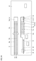
- FIG. 1 is a plan view schematically showing an example of the electronic device 1 according to the present embodiment.
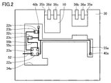
- FIG. 2 is a bottom view of the electronic device shown in FIG.
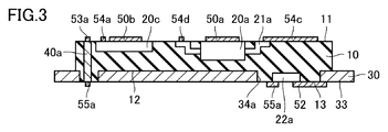
- FIG. 3 is a sectional view taken along the line XX in FIG.
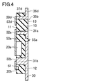
- FIG. 4 is a cross-sectional view taken along line XI-XI of FIG.
- the electronic device 1 can be mounted on various types of electronic devices.
- the electronic device 1 includes the resin molded body 10, the electronic components 20 a, 20 b, and 22 a, the metal plate 30, the heat transfer layer 50 a, and the conductive heat transfer layers 51 and 52.
- the electronic components 20 a, 20 b and 22 a are embedded in the resin molded body 10.
- the metal plate 30 is bonded to the resin molded body 10.
- the surface of the resin molded body 10 includes an upper surface 11 (see FIG. 4) that exposes the electronic components 20a and 20b, and a second lower surface 13 (see FIG. 3) that exposes the electronic component 22a.
- the metal plate 30 has bent portions 31a and 31b.
- the surface of the metal plate 30 includes an end surface 32a of the bent portion 31a and an end surface 32b of the bent portion 31b, which are continuous with the upper surface 11 of the resin molded body 10 (see FIG. 4).
- the surface of the metal plate 30 includes a lower surface 33 continuous with the second lower surface 13 of the resin molded body 10 (see FIG. 3).
- that "the two surfaces are continuous" means that the level difference between the two surfaces is so small that the heat transfer layer, the conductive heat transfer layer and the conductive layer formed thereon are not cut. Do.
- the heat transfer layer 50 a is formed on the upper surface 11 of the resin molded body 10, and is connected to the electronic component 20 a and the tip surface 32 a of the bent portion 31 a of the metal plate 30.
- the conductive heat transfer layer 51 is formed on the upper surface 11 of the resin molded body 10 and is connected to the electrode 21 b of the electronic component 20 b and the tip surface 32 b of the bent portion 31 b of the metal plate 30.
- the heat generated in the electronic components 20 a and 20 b is easily diffused to the metal plate 30 through the heat transfer layer 50 and the conductive heat transfer layer 51. That is, the metal plate 30, the heat transfer layer 50, and the conductive heat transfer layer 51 constitute a heat dissipation structure of the electronic components 20a and 20b.
- the conductive heat transfer layer 52 is formed on the second lower surface 13 of the resin molded body 10 and connected to the electrode 23 a of the electronic component 22 a and the lower surface 33 of the metal plate 30. Thereby, the heat generated in the electronic component 22 a is easily diffused to the metal plate 30 through the conductive heat transfer layer 52. That is, the metal plate 30 and the conductive heat transfer layer 52 constitute a heat dissipation structure of the electronic component 22a.
- the heat transfer layer 50 and the conductive heat transfer layers 51 and 52 are formed on the surface of the resin molded body 10. Therefore, the heat transfer layer 50 and the conductive heat transfer layers 51 and 52 are easily formed by a simple manufacturing method. Furthermore, since the heat transfer layer 50 and the conductive heat transfer layers 51 and 52 are not sealed in the resin, it is not necessary to provide a protective case as in the prior art. As a result, the increase in manufacturing cost can be suppressed.
- the electronic device 1 has a heat dissipation structure capable of suppressing an increase in manufacturing cost.
- the electronic device 1 performs heat transfer from the resin molded body 10, the electronic components 20 a to 20 f and 22 a to 22 c, the metal plates 30 and 36 a to 36 d, the through pins 40 a and 40 b, Layers 50a and 50b, conductive heat transfer layers 51 and 52, and conductive layers 53a to 53d, 54a to 54d, 55a to 55c may be provided.
- each of the electronic components 20a to 20f is referred to as an "electronic component 20".
- each of the electronic components 22a to 22c is referred to as “electronic component 22”.
- each of the metal plates 36a to 36d is referred to as a "metal plate 36”.
- each of the through pins 40a and 40b is referred to as a "through pin 40".
- each of the heat transfer layers 50a and 50b is referred to as a "heat transfer layer 50".
- each of the conductive layers 53a to 53d is referred to as a "conductive layer 53".
- each of the conductive layers 54a to 54d is referred to as a "conductive layer 54".
- each of the conductive layers 55a to 55c is referred to as a "conductive layer 55”.
- the resin molded body 10 is made of, for example, a resin such as polycarbonate (PC), acrylonitrile butadiene styrene (ABS), or polyamide (PA).
- the material of the resin molded body 10 is not particularly limited.
- Resin molded body 10 is, for example, a substantially plate shape having a rectangular shape in a plan view.
- the thickness of the resin molded body 10 is not particularly limited, and is, for example, 3 mm.
- the surface of the resin molded body 10 includes an upper surface 11, a first lower surface 12 joined to the metal plates 30 and 36, and a second lower surface 13 exposed from the metal plate 30 (see FIGS. 3 and 4).
- the metal plates 30, 36 (36a to 36d) are made of, for example, a heat conductive metal such as stainless steel.
- the thickness of the metal plates 30, 36 is not particularly limited, and is, for example, 0.2 mm.
- the metal plates 30 and 36 are joined to the first lower surface 12 of the resin molded body 10.
- the metal plate 30 has a size that covers most of the lower surface of the resin molded body 10.
- the outer size of the metal plate 30 in plan view is larger than the outer size of the resin molded body 10 in plan view.
- Holes 34 a are formed in the metal plate 30.
- the resin molding 10 is filled in the hole 34a. A part of the second lower surface 13 of the resin molded body 10 is exposed from the hole 34 a.
- the metal plate 30 is bent so as to be exposed from the upper surface 11 of the resin molded body 10 and has bent portions 31 a to 31 d embedded in the resin molded body 10.
- the tip end surfaces 32 a and 32 b (see FIG. 4) of the bent portions 31 a and 31 b are exposed from the upper surface 11 of the resin molded body 10 so as to be continuous with the upper surface 11 of the resin molded body 10.
- the tip surfaces of the other bent portions 31 c and 31 d are exposed from the upper surface 11 of the resin molded body 10 so as to be continuous with the upper surface 11 of the resin molded body 10.
- each of the bent portions 31a to 31d is referred to as a "folded portion 31".
- the distal end surfaces of the bent portions 31a to 31d are referred to as "the distal end surface 32".
- the metal plate 30 two notches 35a and 35b (see FIG. 2) are formed.
- the metal plates 36a and 36b are disposed in the notch 35a, and the metal plates 36c and 36d are disposed in the notch 35b.
- the metal plates 36a to 36d respectively have terminal portions 38a to 38d (see FIG. 1) protruding from the resin molded body 10 in a plan view.
- the terminal portions 38a to 38d can be electrically connected to an external device.
- each of the terminals 38a to 38d is referred to as a "terminal 38".
- the resin molded body 10 is filled in part of the notches 35a and 35b. A portion of the second lower surface 13 of the resin molded body 10 is exposed from the notches 35a and 35b.
- the metal plates 36a to 36d are bent so as to be exposed from the upper surface 11 of the resin molded body 10, and have bent portions 37a to 37d embedded in the resin molded body 10, respectively.
- the tip end surface 39 d (see FIG. 4) of the bent portion 37 d is exposed from the upper surface 11 of the resin molded body 10 so as to be continuous with the upper surface 11 of the resin molded body 10.
- the tip surfaces of the other bent portions 37a to 37c are exposed from the upper surface 11 of the resin molded body 10 so as to be continuous with the upper surface 11 of the resin molded body 10.
- each of the bent portions 37a to 37d is referred to as a "folded portion 37".
- the tip end surface of the bent portions 37a to 37d is referred to as "the tip end surface 39".
- the electronic components 20 (20a to 20f) and 22 (22a to 22c) are, for example, passive components (resistors, capacitors, etc.), active components (LSI (Large-Scale Integration), IC (Integrated Circuit), power transistors, etc.), power supplies It is a component selected from a device (battery or the like), a display device (LED (Light Emitting Diode) or the like), a sensor, a switch or the like.
- the electronic components 20a to 20f respectively have electrodes 21a to 21f.
- the electronic components 22a to 22c have electrodes 23a to 23c, respectively.
- Each of the electronic components 20a to 20f and 22a to 22c has a plurality of electrodes, but in the drawing, only one of the plurality of electrodes is denoted by a reference numeral.
- chip-type electronic components 20b, 20d to 20f, 22b, 22c respectively have two electrodes 21c to 21f, 23b, 23c.
- the electronic components 20c and 22a which are ICs have four electrodes 21c and 23a, respectively.
- an electronic component 20a, which is an LSI has six electrodes 21a.
- each of the electrodes 21a to 21f is referred to as an "electrode 21".
- each of the electrodes 23a to 23c is referred to as an "electrode 23”.
- the electronic component 20 is embedded in the resin molded body 10 so as to be exposed from the upper surface 11 of the resin molded body 10. At this time, the electrode 21 is also exposed from the upper surface 11 of the resin molded body 10. The surface of the electronic component 20 exposed from the resin molded body 10 is continuous with the upper surface 11 of the resin molded body 10.
- the electronic component 22 is embedded in the resin molded body 10 so as to be exposed from the second lower surface 13 of the resin molded body 10. At this time, the electrode 23 is also exposed from the second lower surface 13 of the resin molded body 10. The surface of the electronic component 22 exposed from the resin molded body 10 is continuous with the second lower surface 13 of the resin molded body 10.
- the through pins 40 a and 40 b are made of metal and are embedded in the resin molded body 10. One end face of the through pins 40 a and 40 b is exposed from the upper surface 11 of the resin molded body 10 and is continuous with the upper surface 11. The other end surfaces of the through pins 40 a and 40 b are exposed from the second lower surface 13 of the resin molded body 10 and are continuous with the second lower surface 13.
- the heat transfer layer 50 (50a, 50b) is made of a heat transfer material.
- the heat transfer layer 50 may be made of, for example, a conductive metal such as silver having a thermal conductivity of 430 W / mK, or may be made of a nonconductive material such as graphite or a heat conductive resin material.
- the thickness of the heat transfer layer 50 is not particularly limited, and is, for example, 1 to 5 ⁇ m.
- the heat transfer layer 50 is formed on the upper surface 11 of the resin molded body 10, and is connected to the surface of the electronic component 20 and the tip surface 32 of the bent portion 31 of the metal plate 30. Thereby, the heat of the electronic component 20 can be dissipated by transferring it to the metal plate 30.
- the heat transfer layer 50a is connected to the surface (excluding the electrode 21a) of the electronic component 20a and the tip surface 32a of the bent portion 31a.
- the heat transfer layer 50b is connected to the surface of the electronic component 20c and the tip end surface of the bent portion 31c.
- the heat transfer layer 50 is easily formed, for example, by applying a liquid heat transferable ink (for example, silver (Ag) nanoink) to the upper surface 11 of the resin molded body 10 using an inkjet printing method or a screen printing method.
- a liquid heat transferable ink for example, silver (Ag) nanoink
- the inkjet printing method is a printing method in which a liquid ink is ejected from a nozzle and the ink is deposited on the ejection target surface.
- the conductive heat transfer layers 51 and 52 are wirings made of a material having conductivity and heat conductivity.
- Conductive heat transfer layers 51 and 52 are made of, for example, a metal such as silver having a resistivity of 3 to 6 ⁇ cm.
- the thickness of the conductive heat transfer layers 51 and 52 is not particularly limited, and is, for example, 1 to 5 ⁇ m.
- the conductive heat transfer layer 51 is formed on the upper surface 11 of the resin molded body 10.
- the conductive heat transfer layer 51 is connected to the electrode 21b of the electronic component 20b, the electrode 21d of the electronic component 20d, and the tip surface 32b of the bent portion 31b.
- the bent portion 31 b is provided on the metal plate 30. Thereby, the heat of the electronic components 20 b and 20 d is diffused to the metal plate 30. Furthermore, the electronic components 20b and 20d are electrically connected to the metal plate 30, and the metal plate 30 can be used as a ground.
- the conductive heat transfer layer 52 is formed on the second lower surface 13 of the resin molded body 10.
- the conductive heat transfer layer 52 is connected to the electrode 23 a of the electronic component 22 a and the portion of the lower surface 33 of the metal plate 30 around the hole 34 a. Thereby, the heat of the electronic component 22 a is dissipated by the metal plate 30. Furthermore, the electronic component 22a is electrically connected to the metal plate 30, and the metal plate 30 can be used as a ground.
- the conductive heat transfer layers 51 and 52 apply liquid conductive heat transfer ink (for example, silver (Ag) nanoink) to the upper surface 11 or the second lower surface 13 of the resin molded body 10 using, for example, an inkjet printing method or a screen printing method. It is easily formed by doing.
- liquid conductive heat transfer ink for example, silver (Ag) nanoink
- the conductive layers 53 (53a to 53d), 54 (54a to 54d), and 55 (55a to 55c) are wirings made of a conductive material.
- Conductive layers 53, 54, 55 are made of, for example, a metal such as silver having a resistivity of 3 to 6 ⁇ cm.
- the thickness of the conductive layers 53, 54, 55 is not particularly limited, and is, for example, 1 to 5 ⁇ m.
- the conductive layer 53 is formed on the upper surface 11 of the resin molded body 10 and connected to the electrode 21 of the electronic component 20 and the tip surface 39 of the bent portion 37.
- the bent portion 37 is provided on the metal plate 36. As described above, the metal plate 36 has the terminal portion 38 together with the bent portion 37. Therefore, the electronic component 20 connected to the conductive layer 53 can be connected to an external device through the metal plate 36.
- the conductive layer 53a is connected to the electrode 21c of the electronic component 20c, the through pin 40a, and the tip end surface of the bent portion 37a.
- the conductive layer 53b is connected to the electrode 21a of the electronic component 20a, the electrode 21c of the electronic component 20c, and the tip end surface of the bent portion 37b.
- the conductive layer 53c is connected to the electrode 21a of the electronic component 20a, the electrode 21c of the electronic component 20c, and the tip surface of the bent portion 37c.
- the conductive layer 53d is connected to the electrode 21a of the electronic component 20a, the electrode 21e of the electronic component 20e, the electrode 21f of the electronic component 20f, the through pin 40b, and the tip surface 39d of the bent portion 37d.
- the conductive layer 54 is formed on the upper surface 11 of the resin molded body 10 and connected to the electrodes 21 of the plurality of electronic components 20. Thereby, the plurality of electronic components 20 are electrically connected to each other.
- the conductive layer 54a is connected to the electrode 21b of the electronic component 20b and the electrode 21c of the electronic component 20c.
- the conductive layer 54b is connected to the electrode 21a of the electronic component 20a and the electrode 21f of the electronic component 20f.
- the conductive layer 54c is connected to the electrode 21a of the electronic component 20a and the electrode 21e of the electronic component 20e.
- the conductive layer 54d is connected to the electrode 21a of the electronic component 20a and the electrode 21d of the electronic component 20d.
- the conductive layer 55 is formed on the second lower surface 13 of the resin molded body 10 and connected to the electrodes 23 of the plurality of electronic components 22. Thereby, the plurality of electronic components 22 are electrically connected to each other.
- the conductive layer 55a is connected to the electrode 23a of the electronic component 22a, the electrode 23b of the electronic component 22b, the electrode 23c of the electronic component 22c, and the through pins 40a and 40b.
- the conductive layer 55b is connected to the electrode 23a of the electronic component 22a and the electrode 23b of the electronic component 22b.
- the conductive layer 55c is connected to the electrode 23a of the electronic component 22a and the electrode 23c of the electronic component 22c.
- the conductive layers 53, 54, 55 apply a conductive conductive ink (for example, silver (Ag) nano ink) in liquid form to the upper surface 11 or the second lower surface 13 of the resin molded body 10 using, for example, an inkjet printing method or a screen printing method. It is easily formed by doing.
- a conductive conductive ink for example, silver (Ag) nano ink
- the electronic device 1 is manufactured, for example, by the following steps of preparing a metal plate, affixing process, a resin forming process, a peeling process, a layer forming process, and a cutting process.
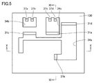
- FIG. 5 is a plan view schematically showing an example of the metal plate 130 which is the source of the metal plates 30, 36a to 36d shown in FIGS.
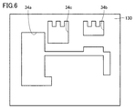
- FIG. 6 is a bottom view of the metal plate 130 shown in FIG.
- FIG. 7 is a sectional view taken along the line XX in FIG.
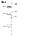
- FIG. 8 is a cross-sectional view taken along line XI-XI in FIG.
- a metal plate 130 having a rectangular shape in plan view is prepared.
- the holes 34a to 34c are formed in the metal plate 130, and a part of the metal plate 130 is bent at a right angle to form bent portions 31a to 31d and 37a to 37d.
- each of the holes 34a to 34c is referred to as a "hole 34".
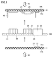
- FIG. 9 is a cross-sectional view schematically showing an example of the attaching process.
- one end surface of the electronic component 20 and the through pin 40 is attached to one surface 80 a of the sheet 80 using an adhesive (not shown).
- the electronic component 20 is attached to the sheet 80 such that the electrode 21 contacts the surface 80 a of the sheet 80.
- the end surface 32 of the bent portion 31 and the end surface 39 of the bent portion 37 in the metal plate 130 are attached.
- the through pin 40 is inserted into the hole 34 of the metal plate 130.
- the sheet 80 for example, polyethylene terephthalate (PET), polyethylene naphthalate (PEN), polyphenylene sulfide (PPS) or the like can be used.
- PET polyethylene terephthalate
- PEN polyethylene naphthalate
- PPS polyphenylene sulfide
- the sheet 80 is preferably made of a material which transmits ultraviolet light and is flexible.
- the electronic component 20, the through pin 40 and the bent portions 31, 37 can be attached to the sheet 80 using, for example, an ultraviolet curing adhesive (not shown) applied to the sheet 80.
- an ultraviolet curing adhesive (not shown) applied to the sheet 80.
- a UV curable adhesive is applied to a surface 80a of a transparent PET sheet 80 having a thickness of 50 ⁇ m to a thickness of 2 to 3 ⁇ m. This application is performed using a method such as inkjet printing.
- the electronic component 20 and the through pin 40 are placed at predetermined positions.
- the metal plate 130 is disposed such that the distal end surface 32 of the bent portion 31 and the distal end surface 39 of the bent portion 37 contact the sheet 80.
- ultraviolet light 82 having an intensity of 3000 mJ / cm 2 is applied from the other surface 80 b of the sheet 80 (that is, the surface opposite to the electronic component 20, the through pin 40 and the bending portions 31 and 37).
- the adhesive cures, and the electronic component 20, one end face of the through pin 40, the end face 32 of the bent portion 31 and the end face 39 of the bent portion 37 are attached to the sheet 80.
- the electronic component 22 is attached to one surface 81 a of the sheet 81 using an adhesive (not shown). At this time, the electronic component 22 is attached to the sheet 81 such that the electrode 23 of the electronic component 22 contacts the surface 81 a of the sheet 81. Further, the lower surface 33 of the metal plate 130 is attached to the sheet 81 so that the hole 34 is covered by the sheet 81. At this time, the metal plate 130 is attached to the sheet 81 such that the electronic component 22 is positioned in the hole 34 formed in the metal plate 130. Furthermore, the other end face of the through pin 40 is also attached to the surface 81 a of the sheet 81.
- the attachment of the electronic component 22, the through pin 40 and the metal plate 130 to the sheet 81 is performed using the same method as the attachment of the electronic component 20, the through pin 40 and the bent portions 31, 37 to the sheet 80. Be That is, the electronic component 22, the through pin 40 and the metal plate 130 are attached to the sheet 81 by irradiating the ultraviolet light 82 from the other surface 81 b of the sheet 81 using an ultraviolet curing adhesive (not shown).
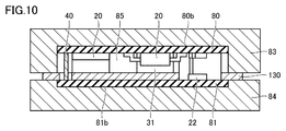
- FIG. 10 is a cross-sectional view schematically showing an example of the sheets 80 and 81, the electronic components 20 and 22, the through pin 40 and the metal plate 130 disposed in the mold.
- the sheets 80 and 81 are disposed between the upper mold 83 and the lower mold 84.
- the sheet 80 is disposed between the upper mold 83 and the lower mold 84 such that the surface 80 b contacts the inner surface of the upper mold 83.
- the sheet 81 is disposed between the upper mold 83 and the lower mold 84 such that the surface 81 b contacts the inner surface of the lower mold 84.
- a space 85 is formed between the upper mold 83 and the lower mold 84.
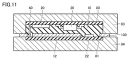
- FIG. 11 is a cross-sectional view schematically showing an example of the resin molding process.
- the resin molded body 10 is formed by injecting the molten resin into the space 85 (see FIG. 10) between the upper mold 83 and the lower mold 84.
- the resin is filled so as to surround the electronic components 20 and 22, the through pin 40 and the bent portions 31 and 37 (see FIG. 9). Therefore, the electronic components 20 and 22, the through pin 40 and the bent portions 31 and 37 are embedded in the resin molded body 10 (see FIGS. 11, 3 and 4). Furthermore, the first lower surface 12 of the resin molded body 10 is bonded to the metal plate 130.
- the conditions for carrying out the injection molding of the resin are appropriately selected according to the material of the resin. For example, when using polycarbonate (PC), injection molding is performed at an injection resin temperature of 270 ° C. and an injection pressure of 100 MPa. When using acrylonitrile butadiene styrene (ABS), injection molding is performed at an injection resin temperature of 180 ° C. and an injection pressure of 20 kgf / cm 2 .
- PC polycarbonate
- ABS acrylonitrile butadiene styrene
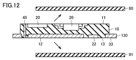
- FIG. 12 is a cross-sectional view schematically showing an example of the peeling step.
- the sheets 80 and 81 are peeled off from the resin molded body 10 taken out of the upper mold 83 and the lower mold 84. By peeling the sheet 80, the upper surface 11 of the resin molded body 10 is exposed.
- the upper surface 11 of the resin molded body 10 is a surface joined to the sheet 80.
- the electronic component 20, one end face of the through pin 40, the end face 32 of the bent portion 31 and the end face 39 of the bent portion 37 are attached to the sheet 80 (see FIG. 9) . Therefore, the surface of the electronic component 20, one end surface of the through pin 40, the end surface 32 of the bent portion 31 and the end surface 39 of the bent portion 37 are continuous with the upper surface 11 of the resin molded body 10 (FIG. 12, FIG. 3, see Figure 4).
- the second lower surface 13 of the resin molded body 10 is exposed.
- the second lower surface 13 of the resin molded body 10 is a surface joined to the sheet 81.
- the electronic component 22, the other end face of the through pin 40, and the lower surface 33 of the metal plate are attached to the sheet 81 (see FIG. 9). Therefore, the surface of the electronic component 22, the other end face of the through pin 40, and the lower surface 33 of the metal plate 130 are continuous with the second lower surface 13 of the resin molded body 10 (see FIGS. 12, 3 and 4).
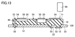
- FIG. 13 is a cross-sectional view schematically showing an example of the layer forming step.
- the heat transfer layer 50, the conductive heat transfer layer 51 (see FIG. 4) and the conductive layers 53 and 54 are formed on the upper surface 11 of the resin molded body 10 using the inkjet printer 90, and The conductive heat transfer layer 52 and the conductive layer 55 are formed on the lower surface 13.
- the heat transfer layer 50, the conductive heat transfer layers 51 and 52, and the conductive layers 53 to 55 may be formed using a screen printing method or the like.
- the materials of the heat transfer layer 50, the conductive heat transfer layers 51 and 52, and the conductive layers 53 to 55 may be the same or different.
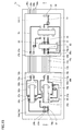
- FIG. 14 is a plan view schematically showing an example of the cutting process.
- the metal plate 130 is divided into the metal plates 30, 36a to 36d by cutting out the cut target portion 131 of the metal plate 30.
- the hole 34b becomes a notch 35a
- the hole 34c becomes a notch 35b (see FIGS. 14 and 2).
- the metal plates 36a to 36d can be used as terminals for connection to an external device, and the metal plate 30 can be used as a part of the heat dissipation structure and a ground. Since the metal plates 30, 36a to 36d are manufactured based on the same metal plate 130, they are made of the same material and have the same thickness.
- the cutting process may be performed before the layer forming process. The cutting process may be omitted depending on the shape of the metal plate 130.
- the heat transfer layer 50 is formed on the upper surface 11 of the resin molded body 10 and is connected to the electronic components 20 a and 20 c and the metal plate 30.
- the conductive heat transfer layer 51 is also formed on the upper surface 11 of the resin molded body 10 and is connected to the electronic component 20 b and the metal plate 30.
- the conductive heat transfer layer 52 is formed on the second lower surface 13 of the resin molded body 10 and is connected to the electronic component 22 a and the metal plate 30.
- the heat generated by the electronic component 22 a is easily diffused to the metal plate 30 through the conductive heat transfer layer 52. That is, the metal plate 30, the heat transfer layer 50, and the conductive heat transfer layers 51, 52 constitute a heat dissipation structure of the electronic components 20a, 20b, 22a.
- the heat transfer layer 50 and the conductive heat transfer layers 51 and 52 are formed on the surface of the resin molded body 10. Therefore, the heat transfer layer 50 and the conductive heat transfer layers 51 and 52 are easily formed by a simple manufacturing method. Furthermore, since the heat transfer layer 50 and the conductive heat transfer layers 51 and 52 are not sealed in the resin, it is not necessary to provide a protective case as in the prior art. As a result, the increase in manufacturing cost can be suppressed. Thus, the electronic device 1 has a heat dissipation structure capable of suppressing an increase in manufacturing cost.
- the electronic component of the control circuit unit is protected by a protective case, but the bonding wire connecting the power semiconductor chip and the thick film substrate is sealed by a sealing resin. Therefore, the stress from the sealing resin may damage the connection between the bonding wire and the power semiconductor chip or the thick film substrate, and the manufacturing quality may be degraded.
- the heat transfer layer 50 and the conductive heat transfer layers 51 and 52 are formed on the surface of the resin molded body 10 after the resin molded body 10 is formed. Therefore, it is possible to suppress the deterioration of the manufacturing quality.
- the metal plate 30 is bent so as to be exposed to the upper surface 11 of the resin molded body 10 and has a bent portion 31 embedded in the resin molded body 10. Thereby, the bondability of the resin molding 10 and the metal plate 30 can be improved. Furthermore, the tip end surface 32 of the bent portion 31 is a surface exposed from the upper surface 11 of the resin molded body 10 so as to be continuous with the upper surface 11 of the resin molded body 10.
- the heat transfer layer 50 and the conductive heat transfer layer 51 are connected to the front end surface 32 of the bent portion 31. Thereby, the heat of the electronic components 20 a and 20 b is easily diffused to the metal plate 30 through the heat transfer layer 50 and the conductive heat transfer layer 51.
- Holes 34 a are formed in the metal plate 30. A portion of the resin molding 10 is filled in the hole 34a.
- the second lower surface 13 of the resin molded body 10 is a surface exposed from the hole 34 a.
- the lower surface 33 of the metal plate 30 is a surface around the hole 34 a and is continuous with the second lower surface 13.
- the conductive heat transfer layer 52 is connected to the lower surface of the metal plate 30. Thereby, the heat of the electronic component 22 a is easily diffused to the metal plate 30 through the conductive heat transfer layer 52.
- the conductive heat transfer layer 51 has conductivity and is connected to the electrode 21 b of the electronic component 20 b and the electrode 21 d of the electronic component 20 d.
- the conductive heat transfer layer 52 has conductivity and is connected to the electrode 23a of the electronic component 22a.
- the electronic device 1 further includes a metal plate 36 bonded to the resin molded body 10.
- the metal plate 36 has a bent portion 37, and the surface of the bent portion 37 includes a tip surface 39 continuous with the top surface 11 of the resin molded body 10.
- the metal plate 36 has a terminal portion 38 connectable to an external device.
- the electronic device 1 further includes a conductive layer 53 connected to the electrode 21 of the electronic component 20 and the tip end surface 39 of the bent portion 37. Therefore, the electronic component 20 can be electrically connected to an external device through the metal plate 36.
- the above-described preparation process of the metal plate, the attaching process, the resin forming process, the peeling process, and the layer forming process are performed.
- the heat transfer layer 50 and the conductive heat transfer layers 51 and 52 are formed on the surface of the resin molded body 10 after the resin molded body 10 is molded.
- the heat transfer layer 50 and the conductive heat transfer layers 51 and 52 are not sealed in the resin, it is not necessary to provide a protective case as in the prior art. As a result, the increase in manufacturing cost can be suppressed.
- the heat transfer layer 50 and the conductive heat transfer layers 51 and 52 are formed on the upper surface 11 or the second lower surface 13 of the resin molded body 10 by, for example, an inkjet printing method. Therefore, high temperature heat treatment such as soldering becomes unnecessary, and it becomes possible to mold the resin molded body 10 using a resin with low heat resistance. As a result, the degree of freedom of the material used for the resin molded body 10 is increased.
- one resin molded body 10 is bonded to the metal plate 30.
- a plurality of resin moldings may be joined to a metal plate, and electronic parts embedded in each of the plurality of resin moldings may be electrically connected via the metal plate.
- FIG. 15 is a plan view schematically showing an electronic device 1a according to a modification.
- FIG. 16 is a bottom view of the electronic device 1a shown in FIG.
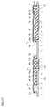
- FIG. 17 is a cross-sectional view taken along the line XX in FIG.
- the example of FIGS. 15 to 17 is different from the electronic device 1 in that the electronic device 1a includes metal plates 73a and 73b instead of the metal plates 36c and 36d.
- the electronic device 1a includes the resin molded body 10a, the electronic components 24a to 24c, 26, the heat transfer layer 56, the conductive heat transfer layers 57, 58, and the conductive layers 59a, 59b, 60a, 60b. , 61, 62a, 62b.
- the resin molded body 10, the electronic components 20, 22, the metal plates 30, 36a, 36b, the through pins 40, the heat transfer layer 50, the conductive heat transfer layers 51, 52, and the conductive layers 53 to 55 are as described above.
- the shapes of the metal plates 30, 36a and 36b, the arrangement of the electronic components 20 and 22, and the arrangement of the heat transfer layer 50, the conductive heat transfer layers 51 and 52, and the conductive layers 53 to 55 are the examples shown in FIGS. It has been changed from.
- the resin molded body 10 a has the same configuration as the resin molded body 10, and is molded separately from the resin molded body 10.
- the electronic components 24a to 24c and 26 are embedded in the resin molded body 10a.
- the electronic components 24a to 24c are exposed from the upper surface 11a of the resin molded body 10a, and the electronic components 26 are exposed from the second lower surface 13a of the resin molded body 10a (see FIG. 17).
- the electrodes 25a to 25c of the electronic components 24a to 24c are also exposed from the upper surface 11a of the resin molded body 10a, and the electrodes 27 of the electronic component 26 are also exposed from the second lower surface 13a of the resin molded body 10a.
- the metal plate 30 is joined not only to the first lower surface 12 of the resin molded body 10 but also to the first lower surface 12 a of the resin molded body 10 a. That is, the metal plate 30 has a size that covers most of the lower surface of the resin molded body 10 and the lower surface of the resin molded body 10a.
- the outer size of the metal plate 30 in plan view is larger than the sum of the outer size of the resin molded body 10 in plan view and the outer size of the resin molded body 10 a in plan view.
- the metal plate 30 is formed with a notch 35a and a hole 34a. A part of the second lower surface 13a of the resin molded body 10a is exposed from the notch 35a. Another part of the second lower surface 13a of the resin molded body 10a is exposed from the hole 34a.
- the metal plate 30 is bent so as to be exposed to the upper surface 11 a of the resin molded body 10 a in addition to the bent portions 31 embedded in the resin molded body 10, and bent portions 70 a and 70 b embedded in the resin molded body 10 a. Have.
- the tip surfaces 71a and 71b of the bent portions 70a and 70b are exposed from the upper surface 11a of the resin molded body 10a so as to be continuous with the upper surface 11a of the resin molded body 10a.
- the metal plates 36 a and 36 b are joined not only to the first lower surface 12 of the resin molded body 10 but also to the first lower surface 12 a of the resin molded body 10 a.
- the metal plates 36a and 36b are bent so as to be exposed from the upper surface 11a of the resin molded body 10a, and have bent portions 72a and 72b embedded in the resin molded body 10a.
- the tip end surfaces of the bent portions 72a and 72b are exposed from the upper surface 11a of the resin molded body 10a so as to be continuous with the upper surface 11a of the resin molded body 10a.
- the metal plates 73 a and 73 b are disposed in the holes 34 a of the metal plate 30.
- the metal plates 73a and 73b include an electronic circuit formed of the electronic components 20 and 22 embedded in the resin molded body 10 and an electronic circuit formed of the electronic components 24a and 26 embedded in the resin molded body 10a. Connect.
- the metal plate 73a is bent to be exposed from the upper surface 11 of the resin molded body 10, and is bent to be exposed from the bent portion 74a embedded in the resin molded body 10 and the upper surface 11a of the resin molded body 10a. And a bent portion 75a embedded in the formed body 10a (see FIGS. 15 and 17).
- the tip end surface 76 a of the bent portion 74 a is exposed from the upper surface 11 of the resin molded body 10 so as to be continuous with the upper surface 11 of the resin molded body 10.
- the tip end surface 77a of the bent portion 75a is exposed from the upper surface 11a of the resin molded body 10a so as to be continuous with the upper surface 11a of the resin molded body 10a.
- the metal plate 73b is bent so as to be exposed from the upper surface 11 of the resin molded body 10, and is bent so as to be exposed from the bent portion 74b embedded in the resin molded body 10 and the upper surface 11a of the resin molded body 10a.
- a bent portion 75b embedded in the resin molded body 10a The tip end surface of the bent portion 74 b is exposed from the upper surface 11 of the resin molded body 10 so as to be continuous with the upper surface 11 of the resin molded body 10.
- the tip end surface of the bent portion 75b is exposed from the upper surface 11a of the resin molded body 10a so as to be continuous with the upper surface 11a of the resin molded body 10a.
- the heat transfer layer 56 has the same configuration as the heat transfer layer 50, is formed on the upper surface 11a of the resin molded body 10a, and is connected to the electronic component 24a and the tip surface 71a of the bent portion 70a. Thereby, the heat of the electronic component 24 a can be diffused to the metal plate 30.
- the conductive heat transfer layer 57 is formed by the same material and manufacturing method as the conductive heat transfer layer 51.
- the conductive heat transfer layer 57 is formed on the upper surface 11a of the resin molded body 10a, and is connected to the electrode 25b of the electronic component 24b and the tip surface 71b of the bent portion 70b.
- the bent portion 70 b is a part of the metal plate 30. Therefore, the heat of the electronic component 24 b is dissipated by the metal plate 30. Furthermore, the electronic component 24b is electrically connected to the metal plate 30, and the metal plate 30 can be used as a ground.
- the conductive heat transfer layer 58 is formed by the same material and manufacturing method as the conductive heat transfer layer 52.
- the conductive heat transfer layer 58 is formed on the second lower surface 13 a of the resin molded body 10 a, and is connected to the electrode 27 of the electronic component 26 and the part of the lower surface 33 of the metal plate 30 around the hole 34 a. Thereby, the heat of the electronic component 26 is dissipated by the metal plate 30. Furthermore, the electronic component 26 is electrically connected to the metal plate 30, and the metal plate 30 can be used as a ground.
- the conductive layers 59a, 59b, 60a, 60b, 61, 62a, 62b are formed by the same material and manufacturing method as the conductive layers 53 to 55.
- the conductive layer 59a is formed on the upper surface 11 of the resin molded body 10, and is connected to the electrode 21 of the electronic component 20 and the tip surface 76a of the bent portion 74a of the metal plate 73a.
- the conductive layer 59 b is formed on the upper surface 11 of the resin molded body 10, and is connected to the electrode 21 of the electronic component 20 and the tip end surface of the bent portion 74 b of the metal plate 73 b.
- the conductive layer 60a is formed on the upper surface 11a of the resin molded body 10a, and is connected to the electrode 25a of the electronic component 24a and the tip surface 77a of the bent portion 75a of the metal plate 73a.
- the conductive layer 60b is formed on the upper surface 11a of the resin molded body 10a, and is connected to the electrode 25a of the electronic component 24a and the tip end surface of the bent portion 75b of the metal plate 73b.
- the electronic component 24a can be electrically connected to the electronic component 20 embedded in the resin molded body 10 through the metal plates 73a and 73b.
- the conductive layer 61 is formed on the second lower surface 13a of the resin molded body 10a, and is connected to the electrode 27 of the electronic component 26 and the lower surface 78 of the metal plate 73a.
- the electronic component 26 can be electrically connected to the electronic component 20 embedded in the resin molded body 10 through the metal plate 73a.
- the conductive layer 62a is formed on the upper surface 11a of the resin molded body 10a, and is connected to the electrode 25c of the electronic component 24c and the tip end surface of the bent portion 72a of the metal plate 36a.
- the conductive layer 62b is formed on the upper surface 11a of the resin molded body 10a, and is connected to the electrode 25c of the electronic component 24c and the tip end surface of the bent portion 72b of the metal plate 36b.
- the electronic component 24c can be electrically connected to an external device through the metal plates 36a and 36b.
- a metal plate which is a base of the metal plates 30, 36a, 36b, 73a, 73b is prepared and cut out into a predetermined pattern. Then, after molding the resin molded body 10, 10a, the metal plate 30, 36a, 36b, 73a, 73b is electrically separated from each other by cutting off the portion to be cut off.
- the electronic device 1a further includes the resin molded body 10a joined to the metal plate 30, and the electronic components 24a and 26 embedded in the resin molded body 10a. And metal plates 73a and 73b joined to the resin molded body 10 and 10a.
- the surface of the resin molded body 10 a includes an upper surface 11 a exposing the electronic component 24 a and a second lower surface 13 a exposing the electronic component 26.
- the metal plate 73a has bent portions 74a and 75a.
- the tip end surface 76 a of the bent portion 74 a is continuous with the upper surface 11 of the resin molded body 10.
- the tip end surface 77a of the bent portion 75a is continuous with the upper surface 11a of the resin molded body 10a. Furthermore, the lower surface 78 of the metal plate 73a is continuous with the second lower surface 13a of the resin molded body 10a.
- the electronic device 1a further includes conductive layers 59a, 60a, 61.
- the conductive layer 59a is formed on the upper surface 11 of the resin molded body 10, and is connected to the electrode 21 of the electronic component 20 and the tip surface 76a of the bent portion 74a.
- the conductive layer 60a is formed on the upper surface 11a of the resin molded body 10a, and is connected to the electrode 25a of the electronic component 24a and the tip end surface 77a of the bent portion 75a.
- the electronic component 24a is electrically connected to the electronic component 20 embedded in the resin molded body 10 through the metal plate 73a.
- the conductive layer 61 is formed on the second lower surface 13a of the resin molded body 10a, and is connected to the electrode 27 of the electronic component 26 and the lower surface 78 of the metal plate 73a.
- the electronic component 26 is electrically connected to the electronic component 20 embedded in the resin molded body 10 through the metal plate 73a.
- complex electronic circuits can be realized.
- the metal plate 73 a is joined to the first lower surface 12 of the resin molded body 10.
- the metal plate 73 a is bent so as to be exposed from the upper surface 11 and has a bent portion 74 a embedded in the resin molded body 10.
- the conductive layer 59a is connected to the tip end surface 76a of the bent portion 74a.
- the metal plate 73a is joined to the first lower surface 12a of the resin molded body 10a.
- the metal plate 73a is bent so as to be exposed from the upper surface 11a, and has a bent portion 75a embedded in the resin molded body 10a.
- the conductive layer 60a is connected to the tip end surface 77a of the bent portion 75a.
- the electronic component 22 is disposed in the hole 34 a of the metal plate 30.
- the electronic component 22 may be disposed in the notches 35 a and 35 b of the metal plate 30.
- a conductive layer may be formed on the second lower surface 13 of the resin molded body 10 to connect the electrode 23 of the electronic component 22 and the lower surface of one of the metal plates 36a to 36d.
- the electronic component 22 is electrically connected to the external device through the metal plates 36a to 36d.
- a conductive heat transfer layer is formed on the second lower surface 13 of the resin molded body 10 to connect the electrode 23 of the electronic component 22 and the portion around the notches 35 a and 35 b in the lower surface 33 of the metal plate 30. Good. Thereby, the heat of the electronic component 22 is diffused to the metal plate 30. Furthermore, the electronic component 22 can use the metal plate 30 as a ground. Similarly, in the examples shown in FIGS. 15 to 17 as well, a conductive layer connecting the electrode 23 of the electronic component 22 and one of the metal plates 73a and 73b is formed on the second lower surface 13 of the resin molded body 10 Good. The electronic component 22 is electrically connected to the electronic components 24a and 26 embedded in the resin molded body 10a via the metal plate 73a.
- the tip end surfaces of the bent portions 31 and 37 are exposed on the upper surface 11 of the resin molded body 10.
- part of the surfaces of the bent portions 31 and 37 may be exposed from the upper surface 11 of the resin molded body 10.
- it may be further bent in an L shape at a predetermined distance from the tips of the bent portions 31 and 37, and the surface from the bent portion to the tip may be exposed from the upper surface 11 of the resin molded body 10.
- the surface area of the bent portions 31 and 37 exposed from the upper surface 11 of the resin molded body 10 is increased, and the heat transfer layer 50, the conductive heat transfer layer 51, and the conductive layer 53 are easily formed.
- the metal plates 30, 36a to 36d were manufactured from the same metal plate 130. However, the metal plate 30 and the metal plates 36a to 36d may be separately prepared and attached to the sheet 80. Similarly, in the first modification, the metal plates 73 a and 73 b and the metal plate 30 may be separately prepared and attached to the sheet 80.
- the electronic device (1, 1a) is joined to the first resin molded body (10), the first electronic component (20, 22) embedded in the first resin molded body, and the first resin molded body (10) And a first metal plate (30).
- the surface of the first resin molded body (10) includes a first surface (upper surface 11, second lower surface 13) for exposing the first electronic component (20, 22).
- the surface of the first metal plate (30) includes a second surface (tip surface 32, lower surface 33) continuous with the first surface (11, 13).
- the electronic device (1, 1a) is further formed on the first surface (11, 13), and is a heat transfer layer (50) connected to the first electronic component (20, 22) and the second surface (32, 33). ,
- the surface of the first resin molded body (10) further includes a third surface (first lower surface 12) on the back side of the first surface (11, 13).
- the first metal plate (30) is joined to the third surface (12).
- the first metal plate (30) has a first bent portion (31) which is bent to be exposed from the first surface (11) and is embedded in the first resin molded body (10).
- the second surface (32) is a surface exposed from the first surface (11) of the first bent portion (31).
- Holes (34a) or notches (35a, 35b) are formed in the first metal plate (30).
- a portion of the first resin molded body (10) is filled in the hole (34a) or the notch (35a, 35b).
- the first surface (13) is a surface exposed from the hole (34a) or the notch (35a, 35b) in the first resin molded body (10).
- the second surface (33) is a surface around the hole (34a) or the notch (35a, 35b) in the first metal plate (30).
- the heat transfer layer (51, 52) has conductivity and is connected to the electrodes (21, 23) of the first electronic component (20, 22).
- the electronic device (1, 1a) further includes a second metal plate (36) joined to the first resin molded body (10).
- the surface of the second metal plate (36) includes a fourth surface (tip surface 39) continuous with the first surface (11, 13).
- the second metal plate (36) has a terminal portion (38) connectable to an external device.
- the electronic device (1, 1a) is formed on the first surface (11, 13), and connected to the electrodes (21, 23) and the fourth surface (39) of the first electronic component (20, 22). It further comprises a conductive layer.
- the electronic device (1a) further includes a second resin molded body (10a) joined to the first metal plate (10), and second electronic components (24a to 24c) embedded in the second resin molded body (10a). , 26), and a third metal plate (73a, 73b) joined to the first resin molded body (10) and the second resin molded body (10a).
- the surface of the second resin molded body (10a) includes a fifth surface (upper surface 11a, second lower surface 13a) for exposing the second electronic component (24a, 24c, 26).
- the surface of the third metal plate (73a, 73b) is a seventh surface (tip surface 76a, lower surface 78) continuous with the first surface (11, 13) and a seventh surface continuous with the fifth surface (11a, 13a) And a surface (tip surface 77a, lower surface 78).
- the electronic device (1a) is further formed on the first surface (11, 13) and connected to the electrodes (21, 23) and the sixth surface (76a, 78) of the first electronic component (20, 22)
- the second conductive layer (59a, 59b) and the fifth surface (11a, 13a) are formed, and the electrodes (25a, 25c, 27) and the seventh surface (77a, 77a) of the second electronic component (24a, 24c, 26) 78) and a third conductive layer (60a, 60b, 61) connected thereto.
- the surface of the first resin molded body (10) further includes a third surface (13) on the back side of the first surface (11).
- the third metal plate (73a, 73b) is joined to the third surface (13).
- the third metal plate (73a, 73b) has a second bent portion (74a, 74b) bent so as to be exposed from the first surface (11) and embedded in the first resin molded body (10).
- the sixth surface (76a) is a surface exposed from the first surface (11) of the second bent portion (74a, 74b).
- the surface of the second resin molded body (10a) further includes an eighth surface (first lower surface 12a) on the back side of the fifth surface (11a).
- the third metal plate (73a, 73b) is joined to the eighth surface (12a).
- the third metal plate (73a, 73b) is bent to be exposed from the fifth surface (11a), and has a third bent portion (75a, 75b) embedded in the second resin molded body (10a).
- the seventh surface (77a) is a surface exposed from the fifth surface (11a) of the third bent portion (75a, 75b).
- the method of manufacturing the electronic device (1, 1a) comprises the steps of forming the holes (34a) or the notches (35a, 35b) in the metal plate (130), and the electronic components (22) being holes (34a, 74) or Bonding the electronic component (22) and the metal plate (130) to one surface (81a) of the sheet (81) so as to be disposed in the notch (35a, 35b); Place the sheet (81) in the mold (83, 84) so that the other side (81b) of) contacts the inner surface of the mold (83, 84), and resin in the mold (83, 84)
- a step of forming the resin molded body (10) in which the electronic component (22) is embedded by being filled, a step of peeling the sheet (81) from the resin molded body (10), and a sheet (81) are peeled Surface of the resin molded body (10) exposed by Forming a heat transfer layer (52) connecting the electronic component (22) and the hole (34a, 74) or the notch (35a, 35b) in the
Landscapes
- Engineering & Computer Science (AREA)
- Microelectronics & Electronic Packaging (AREA)
- Manufacturing & Machinery (AREA)
- Structures Or Materials For Encapsulating Or Coating Semiconductor Devices Or Solid State Devices (AREA)
- Cooling Or The Like Of Semiconductors Or Solid State Devices (AREA)
- Structure Of Printed Boards (AREA)
- Encapsulation Of And Coatings For Semiconductor Or Solid State Devices (AREA)
- Injection Moulding Of Plastics Or The Like (AREA)
Abstract
電子装置は、樹脂成形体と、樹脂成形体に埋設された電子部品と、樹脂成形体に接合された金属板とを備える。樹脂成形体の表面は、第1電子部品を露出させる上面を含む。金属板は折曲部を有し、折曲部の先端面は、樹脂成形体の上面と連続する。電子装置は、さらに、樹脂成形体の上面に形成され、電子部品と折曲部の先端面とに接続する伝熱層を備える。
Description
本発明は、放熱構造を有する電子装置およびその製造方法に関する。
半導体または発光素子などの発熱量の大きな電子部品では、その動作の安定性および長期信頼性の確保のために、発生した熱を外部に放つ必要がある。そのため、リードフレームを用いて電子部品を放熱する技術が開発されている。
たとえば、特開2002-26234号公報(特許文献1)には、放熱板兼用のリードフレームの上にパワー半導体チップおよび制御回路部を搭載し、パワー半導体チップおよび制御回路部を封止樹脂で封止した集積回路が開示されている。制御回路部は、厚膜基板に電子部品が実装された構成を有する。厚膜基板に実装された電子部品は、保護ケースによって覆われる。これにより、封止樹脂からの応力が保護ケースによって遮断され、電子部品が安全に保護される。
特開2002-26234号公報に記載の技術では、封止樹脂からの応力を遮断するために保護ケースを設ける必要があり、製造工程が複雑化して製造コストが増大する。
本開示は、上記の問題点に着目してなされたもので、その目的は、製造コストの増大を抑制することが可能な放熱構造を有する電子装置およびその製造方法を提供することである。
本開示の一例では、電子装置は、第1樹脂成形体と、第1樹脂成形体に埋設された第1電子部品と、第1樹脂成形体に接合された第1金属板とを備える。第1樹脂成形体の表面は、第1電子部品を露出させる第1面を含む。第1金属板の表面は、第1面と連続する第2面を含む。電子装置は、さらに、第1面に形成され、第1電子部品と第2面とに接続する伝熱層を備える。
上記の構成によれば、第1電子部品の熱は、伝熱層を介して第1金属板に拡散される。すなわち、伝熱層および第1金属板は、第1電子部品の放熱構造を構成する。伝熱層は、第1樹脂成形体の表面に形成される。そのため、伝熱層は、簡易な製造方法により容易に形成される。さらに、伝熱層は、樹脂中に封止されないため、従来技術のように保護ケースを設ける必要もない。その結果、製造コストの増大を抑制することができる。このように、電子装置は、製造コストの増大を抑制することが可能な放熱構造を有することができる。
本開示の一例では、第1樹脂成形体の表面は、第1面の裏側の第3面をさらに含む。第1金属板は、第3面に接合される。第1金属板は、第1面から露出するように折り曲げられ、第1樹脂成形体に埋設される第1折曲部を有する。第2面は、第1折曲部における第1面から露出した表面である。
上記の構成によれば、第1樹脂成形体の第1面において、当該第1面と連続する第1折曲部と電子部品とに接続する伝熱層を容易に形成することができる。
本開示の一例では、第1金属板には穴または切欠き部が形成される。第1樹脂成形体の一部は、穴または切欠き部に充填される。第1面は、第1樹脂成形体における穴または切欠き部から露出する面である。第2面は、第1金属板における穴または切欠き部の周囲の表面である。
上記の構成によれば、樹脂成形体の第1面において、第1金属板の穴または切欠き部の周囲と電子部品とに接続する伝熱層を容易に形成することができる。
本開示の一例では、伝熱層は、導電性を有し、第1電子部品の電極に接続する。これにより、たとえば金属板をグランドとして利用することができる。
本開示の一例では、電子装置は、第1樹脂成形体に接合された第2金属板をさらに備える。第2金属板の表面は、第1面と連続する第4面を含む。第2金属板は、外部装置と接続可能な端子部を有する。電子装置は、第1面に形成され、第1電子部品の電極と第4面とに接続する第1導電層をさらに備える。
上記の構成によれば、第1電子部品は、第2金属板を介して外部装置と電気的に接続することができる。
本開示の一例では、電子装置は、さらに、第1金属板に接合された第2樹脂成形体と、第2樹脂成形体に埋設された第2電子部品と、第1樹脂成形体と第2樹脂成形体とに接合された第3金属板とをさらに備える。第2樹脂成形体の表面は、第2電子部品を露出させる第5面を含む。第3金属板の表面は、第1面と連続する第6面と、第5面と連続する第7面とを含む。電子装置は、さらに、第1面に形成され、第1電子部品の電極と第6面とに接続する第2導電層と、第5面に形成され、第2電子部品の電極と第7面とに接続する第3導電層とを備える。
上記の構成によれば、第1金属板に接合された第1樹脂成形体と第2樹脂成形体との各々に埋設された電子部品同士を電気的に接続することができる。その結果、複雑な電子回路を構成することができる。
本開示の一例では、第1樹脂成形体の表面は、第1面の裏側の第3面をさらに含む。第3金属板は、第3面に接合される。第3金属板は、第1面から露出するように折り曲げられ、第1樹脂成形体に埋設される第2折曲部を有する。第6面は、第2折曲部における第1面から露出した表面である。第2樹脂成形体の表面は、第5面の裏側の第8面をさらに含む。第3金属板は、第8面に接合される。第3金属板は、第5面から露出するように折り曲げられ、第2樹脂成形体に埋設される第3折曲部を有する。第7面は、第3折曲部における第5面から露出した表面である。
上記の構成によれば、第1樹脂成形体の第1面において、当該第1面と連続する第2折曲部と第1電子部品とに接続する第2導電層を容易に形成することができる。第2樹脂成形体の第5面において、当該第5面と連続する第3折曲部と第2電子部品とに接続する第3導電層を容易に形成することができる。
本開示の一例では、電子装置の製造方法は、以下の第1~第5工程を備える。第1工程は、金属板の一部を折り曲げて、折曲部を形成する工程である。第2工程は、電子部品と折曲部の先端面とをシートの一方の面に貼り付ける工程である。第3工程は、シートの他方の面が成形型の内面に接するようにシートを成形型内に配置し、成形型内に樹脂を充填させることにより、電子部品と折曲部とが埋設された樹脂成形体を成形する工程である。第4工程は、樹脂成形体からシートを剥離する工程である。第5工程は、シートを剥離することにより露出した樹脂成形体の表面に、電子部品と折曲部とに接続する伝熱層を形成する工程である。
本開示の一例では、電子装置の製造方法は、以下の第1~第5工程を備える。第1工程は、金属板に穴または切欠き部を形成する工程である。第2工程は、電子部品が穴または切欠き部の中に配置されるように、電子部品と金属板とをシートの一方の面に貼り付ける工程である。第3工程は、シートの他方の面が成形型の内面に接するようにシートを成形型内に配置し、成形型内に樹脂を充填させることにより、電子部品が埋設された樹脂成形体を成形する工程である。第4工程は、樹脂成形体からシートを剥離する工程である。第5工程は、シートを剥離することにより露出した樹脂成形体の表面に、電子部品と金属板における穴または切欠き部の周囲とに接続する伝熱層を形成する工程である。
上記のいずれかの製造方法によれば、伝熱層は、樹脂成形体の成形後に、樹脂成形体の表面に形成される。そのため、伝熱層は、簡易な製造方法により容易に形成される。さらに、伝熱層は、樹脂中に封止されないため、従来技術のように保護ケースを設ける必要もない。その結果、製造コストの増大を抑制することができる。さらに、電子部品の熱は、伝熱層を介して金属板に拡散される。すなわち、伝熱層および金属板は、電子部品の放熱構造を構成する。
本開示によれば、製造コストの増大を抑制することが可能な放熱構造を有する電子装置およびその製造方法を提供することができる。
<適用例>
図1~図4を参照して、本発明が適用される場面の一例について説明する。図1は、本実施形態に係る電子装置1の一例を模式的に示す平面図である。図2は、図1に示す電子装置の底面図である。図3は、図1のX-X線に沿った矢視断面図である。図4は、図1のXI-XIに沿った矢視断面図である。電子装置1は、様々な種類の電子機器に搭載可能である。
図1~図4を参照して、本発明が適用される場面の一例について説明する。図1は、本実施形態に係る電子装置1の一例を模式的に示す平面図である。図2は、図1に示す電子装置の底面図である。図3は、図1のX-X線に沿った矢視断面図である。図4は、図1のXI-XIに沿った矢視断面図である。電子装置1は、様々な種類の電子機器に搭載可能である。
図1~図4に示す例では、電子装置1は、樹脂成形体10と、電子部品20a,20b,22aと、金属板30と、伝熱層50aと、導電伝熱層51,52とを備える。電子部品20a,20b,22aは、樹脂成形体10に埋設される。金属板30は、樹脂成形体10に接合される。
樹脂成形体10の表面は、電子部品20a,20bを露出させる上面11(図4参照)と、電子部品22aを露出させる第2下面13(図3参照)とを含む。金属板30は折曲部31a,31bを有する。金属板30の表面は、樹脂成形体10の上面11に連続する、折曲部31aの先端面32aと折曲部31bの先端面32bとを含む(図4参照)。さらに、金属板30の表面は、樹脂成形体10の第2下面13に連続する下面33を含む(図3参照)。ここで、2つの面が「連続する」とは、当該2つの面の間の段差が、その上に形成される伝熱層、導電伝熱層および導電層が切断しない程度に小さいことを意味する。
伝熱層50aは、樹脂成形体10の上面11に形成され、電子部品20aと金属板30における折曲部31aの先端面32aとに接続する。導電伝熱層51は、樹脂成形体10の上面11に形成され、電子部品20bの電極21bと金属板30における折曲部31bの先端面32bとに接続する。これにより、電子部品20a,20bで生じた熱は、伝熱層50,導電伝熱層51を介して金属板30にそれぞれ拡散しやすくなる。すなわち、金属板30、伝熱層50および導電伝熱層51は、電子部品20a,20bの放熱構造を構成する。
同様に、導電伝熱層52は、樹脂成形体10の第2下面13に形成され、電子部品22aの電極23aと金属板30の下面33とに接続する。これにより、電子部品22aで生じた熱は、導電伝熱層52を介して金属板30に拡散しやすくなる。すなわち、金属板30と導電伝熱層52とは、電子部品22aの放熱構造を構成する。
伝熱層50および導電伝熱層51,52は、樹脂成形体10の表面に形成される。そのため、伝熱層50および導電伝熱層51,52は、簡易な製造方法により容易に形成される。さらに、伝熱層50および導電伝熱層51,52は、樹脂中に封止されないため、従来技術のように保護ケースを設ける必要もない。その結果、製造コストの増大を抑制することができる。
以上のように、実施の形態に係る電子装置1は、製造コストの増大を抑制することが可能な放熱構造を有する。
<構成例>
以下に電子装置1の各構成の詳細を説明する。図1~図4に示す例では、電子装置1は、樹脂成形体10と、電子部品20a~20f,22a~22cと、金属板30,36a~36dと、貫通ピン40a,40bと、伝熱層50a,50bと、導電伝熱層51,52と、導電層53a~53d,54a~54d,55a~55cとを備えてもよい。
以下に電子装置1の各構成の詳細を説明する。図1~図4に示す例では、電子装置1は、樹脂成形体10と、電子部品20a~20f,22a~22cと、金属板30,36a~36dと、貫通ピン40a,40bと、伝熱層50a,50bと、導電伝熱層51,52と、導電層53a~53d,54a~54d,55a~55cとを備えてもよい。
以下では、電子部品20a~20fを特に区別しない場合、電子部品20a~20fの各々を「電子部品20」という。電子部品22a~22cを特に区別しない場合、電子部品22a~22cの各々を「電子部品22」という。金属板36a~36dを特に区別しない場合、金属板36a~36dの各々を「金属板36」という。貫通ピン40a,40bを特に区別しない場合、貫通ピン40a,40bの各々を「貫通ピン40」という。伝熱層50a,50bを特に区別しない場合、伝熱層50a,50bの各々を「伝熱層50」という。導電層53a~53dを特に区別しない場合、導電層53a~53dの各々を「導電層53」という。導電層54a~54dを特に区別しない場合、導電層54a~54dの各々を「導電層54」という。導電層55a~55cを特に区別しない場合、導電層55a~55cの各々を「導電層55」という。
樹脂成形体10は、たとえばポリカーボネイト(PC)、アクリロニトリルブタジエンスチレン(ABS)、ポリアミド(PA)等の樹脂からなる。ただし、樹脂成形体10の材質は、特に限定されるものではない。樹脂成形体10は、たとえば平面視矩形状の略板状である。樹脂成形体10の厚みは特に限定されず、たとえば3mmである。樹脂成形体10の表面は、上面11と、金属板30,36と接合する第1下面12と、金属板30から露出する第2下面13とを含む(図3,図4参照)。
金属板30,36(36a~36d)は、たとえばステンレス等の伝熱性を有する金属で構成される。金属板30,36の厚みは特に限定されず、たとえば0.2mmである。金属板30,36は、樹脂成形体10の第1下面12に接合される。
金属板30は、樹脂成形体10の下面の大部分を覆うサイズを有する。金属板30の平面視の外形サイズは、樹脂成形体10の平面視の外形サイズよりも大きい。金属板30には穴34a(図2参照)が形成される。穴34aには樹脂成形体10が充填される。樹脂成形体10の第2下面13の一部は、穴34aから露出する。
金属板30は、樹脂成形体10の上面11から露出するように折り曲げられ、樹脂成形体10に埋設される折曲部31a~31dを有する。折曲部31a,31bのそれぞれの先端面32a、32b(図4参照)は、樹脂成形体10の上面11に連続するように、樹脂成形体10の上面11から露出する。他の折曲部31c,31dの先端面も同様に、樹脂成形体10の上面11に連続するように、樹脂成形体10の上面11から露出する。以下では、折曲部31a~31dを特に区別しない場合、折曲部31a~31dの各々を「折曲部31」という。折曲部31a~31dの先端面を特に区別しない場合、折曲部31a~31dの先端面を「先端面32」という。
金属板30には2つの切欠き部35a,35b(図2参照)が形成される。切欠き部35a内に金属板36a,36bが配置され、切欠き部35b内に金属板36c,36dが配置される。金属板36a~36dは、平面視において樹脂成形体10から突出した端子部38a~38d(図1参照)をそれぞれ有する。端子部38a~38dは、外部装置と電気的に接続可能である。以下では、端子部38a~38dを特に区別しない場合、端子部38a~38dの各々を「端子部38」という。切欠き部35a,35bの一部には樹脂成形体10が充填される。樹脂成形体10の第2下面13の一部は、切欠き部35a,35bから露出する。
金属板36a~36dは、樹脂成形体10の上面11から露出するように折り曲げられ、樹脂成形体10に埋設される折曲部37a~37dをそれぞれ有する。折曲部37dの先端面39d(図4参照)は、樹脂成形体10の上面11に連続するように、樹脂成形体10の上面11から露出する。他の折曲部37a~37cの先端面も同様に、樹脂成形体10の上面11に連続するように、樹脂成形体10の上面11から露出する。以下では、折曲部37a~37dを特に区別しない場合、折曲部37a~37dの各々を「折曲部37」という。折曲部37a~37dの先端面を特に区別しない場合、折曲部37a~37dの先端面を「先端面39」という。
電子部品20(20a~20f),22(22a~22c)は、たとえば受動部品(抵抗、コンデンサ等)、能動部品(LSI(Large-Scale Integration)、IC(Integrated Circuit)、パワートランジスタ等)、電源装置(電池等)、表示装置(LED(Light Emitting Diode)等)、センサ、スイッチ等から選択される部品である。
電子部品20a~20fは、電極21a~21fをそれぞれ有する。電子部品22a~22cは、電極23a~23cをそれぞれ有する。電子部品20a~20f,22a~22cの各々は複数の電極を有するが、図中には当該複数の電極のうちの一つにのみ符号を付している。たとえば、チップ型の電子部品20b,20d~20f,22b,22cは2つの電極21c~21f,23b,23cをそれぞれ有する。たとえばICである電子部品20c,22aは4つの電極21c,23aをそれぞれ有する。たとえばLSIである電子部品20aは6つの電極21aを有する。以下では、電極21a~21fを特に区別しない場合、電極21a~21fの各々を「電極21」という。さらに、電極23a~23cを特に区別しない場合、電極23a~23cの各々を「電極23」という。
電子部品20は、樹脂成形体10の上面11から露出するように、樹脂成形体10に埋設される。このとき、電極21も樹脂成形体10の上面11から露出する。電子部品20の表面のうち樹脂成形体10から露出する面は、樹脂成形体10の上面11と連続する。
電子部品22は、樹脂成形体10の第2下面13から露出するように、樹脂成形体10に埋設される。このとき、電極23も樹脂成形体10の第2下面13から露出する。電子部品22の表面のうち樹脂成形体10から露出する面は、樹脂成形体10の第2下面13と連続する。
貫通ピン40a,40bは、金属製であり、樹脂成形体10に埋設される。貫通ピン40a,40bの一方の端面は、樹脂成形体10の上面11から露出し、上面11と連続する。貫通ピン40a,40bの他方の端面は、樹脂成形体10の第2下面13から露出し、第2下面13と連続する。
伝熱層50(50a,50b)は、伝熱材で構成される。伝熱層50は、たとえば熱伝導率430W/mKの銀等の導電性の金属で構成されてもよいし、グラファイト、熱伝導樹脂材等の非導電性の材料で構成されてもよい。伝熱層50の厚みは特に限定されず、たとえば1~5μmである。伝熱層50は、樹脂成形体10の上面11に形成され、電子部品20の表面と金属板30の折曲部31の先端面32とに接続する。これにより、電子部品20の熱を金属板30に伝えることにより放熱することができる。
図1~図4に示す例では、伝熱層50aは、電子部品20aの表面(電極21aを除く)と折曲部31aの先端面32aとに接続する。伝熱層50bは、電子部品20cの表面と折曲部31cの先端面とに接続する。
伝熱層50は、たとえばインクジェット印刷法やスクリーン印刷法を用いて液状の伝熱性インク(たとえば、銀(Ag)ナノインク)を樹脂成形体10の上面11に塗布することにより、容易に形成される。インクジェット印刷法は、液状のインクをノズルから噴射し、インクを噴射対象面上に堆積させる印刷方式である。
導電伝熱層51,52は、導電性および伝熱性を有する材料で構成される配線である。導電伝熱層51,52は、たとえば抵抗率3~6μΩcmの銀等の金属で構成される。導電伝熱層51,52の厚みは特に限定されず、たとえば1~5μmである。
導電伝熱層51は、樹脂成形体10の上面11に形成される。導電伝熱層51は、電子部品20bの電極21bと電子部品20dの電極21dと折曲部31bの先端面32bとに接続する。折曲部31bは金属板30に備えられる。これにより、電子部品20b,20dの熱が金属板30に拡散される。さらに、電子部品20b,20dは、金属板30と電気的に接続され、金属板30をグランドとして利用できる。
導電伝熱層52は、樹脂成形体10の第2下面13に形成される。導電伝熱層52は、電子部品22aの電極23aと金属板30の下面33における穴34aの周囲の部分とに接続する。これにより、電子部品22aの熱が金属板30によって放熱される。さらに、電子部品22aは、金属板30と電気的に接続され、金属板30をグランドとして利用できる。
導電伝熱層51,52は、たとえばインクジェット印刷法やスクリーン印刷法を用いて液状の導電伝熱性インク(たとえば、銀(Ag)ナノインク)を樹脂成形体10の上面11または第2下面13に塗布することにより、容易に形成される。
導電層53(53a~53d),54(54a~54d),55(55a~55c)は、導電性を有する材料で構成される配線である。導電層53,54,55は、たとえば抵抗率3~6μΩcmの銀等の金属で構成される。導電層53,54,55の厚みは特に限定されず、たとえば1~5μmである。
導電層53は、樹脂成形体10の上面11に形成され、電子部品20の電極21と折曲部37の先端面39とに接続する。折曲部37は金属板36に備えられる。上述したように、金属板36は、折曲部37とともに端子部38を有する。そのため、導電層53と接続される電子部品20は、金属板36を介して外部装置と接続できる。
図1および図4に示す例では、導電層53aは、電子部品20cの電極21cと貫通ピン40aと折曲部37aの先端面とに接続する。導電層53bは、電子部品20aの電極21aと電子部品20cの電極21cと折曲部37bの先端面とに接続する。導電層53cは、電子部品20aの電極21aと電子部品20cの電極21cと折曲部37cの先端面とに接続する。導電層53dは、電子部品20aの電極21aと電子部品20eの電極21eと電子部品20fの電極21fと貫通ピン40bと折曲部37dの先端面39dとに接続する。
導電層54は、樹脂成形体10の上面11に形成され、複数の電子部品20の電極21に接続する。これにより、複数の電子部品20同士が電気的に接続される。図1,図3および図4に示す例では、導電層54aは、電子部品20bの電極21bと電子部品20cの電極21cとに接続する。導電層54bは、電子部品20aの電極21aと電子部品20fの電極21fとに接続する。導電層54cは、電子部品20aの電極21aと電子部品20eの電極21eとに接続する。導電層54dは、電子部品20aの電極21aと電子部品20dの電極21dとに接続する。
導電層55は、樹脂成形体10の第2下面13に形成され、複数の電子部品22の電極23に接続する。これにより、複数の電子部品22同士が電気的に接続される。導電層55aは、電子部品22aの電極23aと電子部品22bの電極23bと電子部品22cの電極23cと貫通ピン40a,40bとに接続する。導電層55bは、電子部品22aの電極23aと電子部品22bの電極23bとに接続する。導電層55cは、電子部品22aの電極23aと電子部品22cの電極23cとに接続する。
導電層53,54,55は、たとえばインクジェット印刷法やスクリーン印刷法を用いて液状の導電伝熱性インク(たとえば、銀(Ag)ナノインク)を樹脂成形体10の上面11または第2下面13に塗布することにより、容易に形成される。
<電子装置の製造方法>
次に、図5~図14を参照して、電子装置1の製造方法の一例について説明する。電子装置1は、たとえば以下に示す金属板の準備工程、貼り付け工程、樹脂成形工程、剥離工程、層形成工程、切取工程によって製造される。
次に、図5~図14を参照して、電子装置1の製造方法の一例について説明する。電子装置1は、たとえば以下に示す金属板の準備工程、貼り付け工程、樹脂成形工程、剥離工程、層形成工程、切取工程によって製造される。
(金属板の準備工程)
図5~図8を参照して、金属板の準備工程の一例について説明する。図5は、図1~図4に示す金属板30,36a~36dの元となる金属板130の一例を模式的に示す平面図である。図6は、図5に示す金属板130の底面図である。図7は、図5のX-X線に沿った矢視断面図である。図8は、図5のXI-XI線に沿った矢視断面図である。
図5~図8を参照して、金属板の準備工程の一例について説明する。図5は、図1~図4に示す金属板30,36a~36dの元となる金属板130の一例を模式的に示す平面図である。図6は、図5に示す金属板130の底面図である。図7は、図5のX-X線に沿った矢視断面図である。図8は、図5のXI-XI線に沿った矢視断面図である。
図5~図8の例では、平面視矩形状の金属板130が準備される。金属板130を準備する工程では、金属板130に穴34a~34cを形成するとともに、金属板130の一部を直角に曲げて、折曲部31a~31d,37a~37dを形成する。以下では、穴34a~34cを特に区別しない場合、穴34a~34cの各々を「穴34」という。
(貼り付け工程)
図9は、貼り付け工程の一例を模式的に示す断面図である。図9の例では、電子部品20および貫通ピン40の一方の端面が接着剤(図示せず)を用いてシート80の一方の面80aに貼り付けられる。このとき、電極21がシート80の面80aに接触するように、電子部品20はシート80に貼り付けられる。さらに、シート80の面80aには、金属板130における、折曲部31の先端面32と折曲部37の先端面39とが貼り付けられる。このとき、貫通ピン40は、金属板130の穴34に挿入される。
図9は、貼り付け工程の一例を模式的に示す断面図である。図9の例では、電子部品20および貫通ピン40の一方の端面が接着剤(図示せず)を用いてシート80の一方の面80aに貼り付けられる。このとき、電極21がシート80の面80aに接触するように、電子部品20はシート80に貼り付けられる。さらに、シート80の面80aには、金属板130における、折曲部31の先端面32と折曲部37の先端面39とが貼り付けられる。このとき、貫通ピン40は、金属板130の穴34に挿入される。
シート80の材料としては、たとえば、ポリエチレンテレフタレート(PET)、ポリエチレンナフタレート(PEN)、ポリフェニレンサルファイド(PPS)等を用いることができる。シート80は、紫外線を透過し、かつ柔軟性を有している材料からなっていることが好ましい。
シート80への電子部品20,貫通ピン40および折曲部31,37の貼り付けは、たとえば、シート80に塗布した紫外線硬化型の接着剤(図示せず)を用いて行なうことができる。たとえば、厚さ50μmの透明PET製のシート80の面80aに、紫外線硬化型の接着剤を2~3μmの厚さで塗布する。この塗布は、たとえばインクジェット印刷法などの方法を用いて行なわれる。その後、電子部品20と貫通ピン40とを所定位置に置く。さらに、折曲部31の先端面32と折曲部37の先端面39とがシート80に接触するように金属板130を配置する。シート80の他方の面80b(つまり、電子部品20,貫通ピン40および折曲部31,37とは反対側の面)から、たとえば3000mJ/cm2の強度の紫外線82を照射する。これにより、接着剤が硬化し、電子部品20,貫通ピン40の一方の端面、折曲部31の先端面32および折曲部37の先端面39がシート80に貼り付けられる。
さらに、電子部品22が接着剤(図示せず)を用いてシート81の一方の面81aに貼り付けられる。このとき、電子部品22の電極23がシート81の面81aに接触するように、電子部品22はシート81に貼り付けられる。さらに、シート81によって穴34が覆われるように、金属板130の下面33がシート81に貼り付けられる。このとき、電子部品22が金属板130に形成された穴34内に位置するように、シート81に金属板130が貼り付けられる。さらに、貫通ピン40に他方の端面もシート81の面81aに貼り付けられる。
シート81への電子部品22、貫通ピン40および金属板130の貼り付けは、シート80への電子部品20,貫通ピン40および折曲部31,37の貼り付け方法と同一の方法を用いて行なわれる。すなわち、図示しない紫外線硬化型の接着剤を用いて紫外線82をシート81の他方の面81bから照射することにより、電子部品22、貫通ピン40および金属板130がシート81に貼り付けられる。
(樹脂成形工程)
図10は、成形型の中に配置されたシート80,81、電子部品20,22、貫通ピン40および金属板130の一例を模式的に示す断面図である。図10に示す例では、シート80,81が上成形型83と下成形型84との間に配置される。このとき、面80bが上成形型83の内面に接するように、シート80は上成形型83と下成形型84との間に配置される。さらに、面81bが下成形型84の内面に接するように、シート81は上成形型83と下成形型84との間に配置される。これにより、上成形型83と下成形型84との間には空間85が形成される。
図10は、成形型の中に配置されたシート80,81、電子部品20,22、貫通ピン40および金属板130の一例を模式的に示す断面図である。図10に示す例では、シート80,81が上成形型83と下成形型84との間に配置される。このとき、面80bが上成形型83の内面に接するように、シート80は上成形型83と下成形型84との間に配置される。さらに、面81bが下成形型84の内面に接するように、シート81は上成形型83と下成形型84との間に配置される。これにより、上成形型83と下成形型84との間には空間85が形成される。
図11は、樹脂成形工程の一例を模式的に示す断面図である。上成形型83と下成形型84との間の空間85(図10参照)に溶融樹脂を射出することにより、樹脂成形体10を成形する。樹脂は、電子部品20,22、貫通ピン40および折曲部31,37(図9参照)を囲むように充填される。そのため、電子部品20,22、貫通ピン40および折曲部31,37は、樹脂成形体10に埋設される(図11、図3および図4参照)。さらに、樹脂成形体10の第1下面12は金属板130と接合する。
樹脂の射出成形を行なう条件は、樹脂の材料に応じて適宜選択される。たとえば、ポリカーボネート(PC)を用いる場合には、射出樹脂温度270℃、射出圧力100MPaで射出成形を行なう。アクリロニトリルブタジエンスチレン(ABS)を用いる場合には、射出樹脂温度180℃、射出圧力20kgf/cm2で射出成形を行なう。
(剥離工程)
図12は、剥離工程の一例を模式的に示す断面図である。上成形型83と下成形型84とから取り出された樹脂成形体10からシート80,81を剥離する。シート80を剥離することにより、樹脂成形体10の上面11が露出する。樹脂成形体10の上面11は、シート80と接合していた面である。上記の貼り付け工程において、シート80には、電子部品20、貫通ピン40の一方の端面、折曲部31の先端面32および折曲部37の先端面39が貼り付けられる(図9参照)。そのため、電子部品20の表面、貫通ピン40の一方の端面、折曲部31の先端面32および折曲部37の先端面39は、樹脂成形体10の上面11と連続する(図12、図3、図4参照)。
図12は、剥離工程の一例を模式的に示す断面図である。上成形型83と下成形型84とから取り出された樹脂成形体10からシート80,81を剥離する。シート80を剥離することにより、樹脂成形体10の上面11が露出する。樹脂成形体10の上面11は、シート80と接合していた面である。上記の貼り付け工程において、シート80には、電子部品20、貫通ピン40の一方の端面、折曲部31の先端面32および折曲部37の先端面39が貼り付けられる(図9参照)。そのため、電子部品20の表面、貫通ピン40の一方の端面、折曲部31の先端面32および折曲部37の先端面39は、樹脂成形体10の上面11と連続する(図12、図3、図4参照)。
シート81を剥離することにより、樹脂成形体10の第2下面13が露出する。樹脂成形体10の第2下面13は、シート81と接合していた面である。上記の貼り付け工程において、シート81には、電子部品22、貫通ピン40の他方の端面および金属板の下面33が貼り付けられる(図9参照)。そのため、電子部品22の表面、貫通ピン40の他方の端面および金属板130の下面33は、樹脂成形体10の第2下面13と連続する(図12、図3、図4参照)。
(層形成工程)
図13は、層形成工程の一例を模式的に示す断面図である。たとえばインクジェット印刷機90を用いて、樹脂成形体10の上面11に伝熱層50、導電伝熱層51(図4参照)および導電層53,54を形成するとともに、樹脂成形体10の第2下面13に導電伝熱層52および導電層55を形成する。伝熱層50、導電伝熱層51,52および導電層53~55の形成は、スクリーン印刷法等を用いて行なわれてもよい。伝熱層50、導電伝熱層51,52および導電層53~55との材料は同一であってもよいし、異なっていてもよい。
図13は、層形成工程の一例を模式的に示す断面図である。たとえばインクジェット印刷機90を用いて、樹脂成形体10の上面11に伝熱層50、導電伝熱層51(図4参照)および導電層53,54を形成するとともに、樹脂成形体10の第2下面13に導電伝熱層52および導電層55を形成する。伝熱層50、導電伝熱層51,52および導電層53~55の形成は、スクリーン印刷法等を用いて行なわれてもよい。伝熱層50、導電伝熱層51,52および導電層53~55との材料は同一であってもよいし、異なっていてもよい。
(切取工程)
図14は、切取工程の一例を模式的に示す平面図である。金属板30の切取対象部分131を切り取ることにより、金属板130を金属板30,36a~36dに分割する。このとき、穴34bは切欠き部35aとなり、穴34cは切欠き部35bとなる(図14,図2参照)。これにより、金属板36a~36dを外部装置との接続用の端子として利用するとともに、金属板30を放熱構造の一部およびグランドとして利用することができる。金属板30,36a~36dは、同一の金属板130を基に作製されるため、同一の材料で構成され、同一の厚みを有する。切取工程は、層形成工程の前に行なわれてもよい。切取工程は、金属板130の形状に応じて省略されてもよい。
図14は、切取工程の一例を模式的に示す平面図である。金属板30の切取対象部分131を切り取ることにより、金属板130を金属板30,36a~36dに分割する。このとき、穴34bは切欠き部35aとなり、穴34cは切欠き部35bとなる(図14,図2参照)。これにより、金属板36a~36dを外部装置との接続用の端子として利用するとともに、金属板30を放熱構造の一部およびグランドとして利用することができる。金属板30,36a~36dは、同一の金属板130を基に作製されるため、同一の材料で構成され、同一の厚みを有する。切取工程は、層形成工程の前に行なわれてもよい。切取工程は、金属板130の形状に応じて省略されてもよい。
<作用・効果>
以上のように、本実施の形態に係る電子装置1では、伝熱層50は、樹脂成形体10の上面11に形成され、電子部品20a,20cと金属板30とに接続する。導電伝熱層51も、樹脂成形体10の上面11に形成され、電子部品20bと金属板30とに接続する。導電伝熱層52は、樹脂成形体10の第2下面13に形成され、電子部品22aと金属板30とに接続する。これにより、電子部品20a,20bで生じた熱は、伝熱層50または導電伝熱層51を介して金属板30に拡散しやすくなる。同様に、電子部品22aで生じた熱は、導電伝熱層52を介して金属板30に拡散しやすくなる。すなわち、金属板30、伝熱層50および導電伝熱層51,52は、電子部品20a,20b,22aの放熱構造を構成する。
以上のように、本実施の形態に係る電子装置1では、伝熱層50は、樹脂成形体10の上面11に形成され、電子部品20a,20cと金属板30とに接続する。導電伝熱層51も、樹脂成形体10の上面11に形成され、電子部品20bと金属板30とに接続する。導電伝熱層52は、樹脂成形体10の第2下面13に形成され、電子部品22aと金属板30とに接続する。これにより、電子部品20a,20bで生じた熱は、伝熱層50または導電伝熱層51を介して金属板30に拡散しやすくなる。同様に、電子部品22aで生じた熱は、導電伝熱層52を介して金属板30に拡散しやすくなる。すなわち、金属板30、伝熱層50および導電伝熱層51,52は、電子部品20a,20b,22aの放熱構造を構成する。
伝熱層50および導電伝熱層51,52は、樹脂成形体10の表面に形成される。そのため、伝熱層50および導電伝熱層51,52は、簡易な製造方法により容易に形成される。さらに、伝熱層50および導電伝熱層51,52は、樹脂中に封止されないため、従来技術のように保護ケースを設ける必要もない。その結果、製造コストの増大を抑制することができる。このように、電子装置1は、製造コストの増大を抑制することが可能な放熱構造を有する。
さらに、特開2002-26234号公報では、制御回路部の電子部品は保護ケースによって保護されるが、パワー半導体チップと厚膜基板とを接続するボンディングワイヤは封止樹脂によって封止される。そのため、封止樹脂からの応力によって、当該ボンディングワイヤとパワー半導体チップまたは厚膜基板との接続部が破損する可能性があり、製造品質が低下する。しかしながら、伝熱層50および導電伝熱層51,52は、樹脂成形体10を成形した後に、樹脂成形体10の表面に形成される。そのため、製造品質の低下を抑制することができる。
金属板30は、樹脂成形体10の上面11に露出するように折り曲げられ、樹脂成形体10に埋設される折曲部31を有する。これにより、樹脂成形体10と金属板30との接合性を高めることができる。さらに、折曲部31の先端面32は、樹脂成形体10の上面11に連続するように、樹脂成形体10の上面11から露出する面である。伝熱層50および導電伝熱層51は折曲部31の先端面32に接続する。これにより、電子部品20a,20bの熱は、伝熱層50および導電伝熱層51を介して金属板30に容易に拡散される。
金属板30には穴34aが形成される。樹脂成形体10の一部は、穴34aに充填される。樹脂成形体10の第2下面13は、穴34aから露出する面である。金属板30の下面33は、穴34aの周囲の面であり、第2下面13と連続する。導電伝熱層52は、金属板30の下面に接続する。これにより、電子部品22aの熱は、導電伝熱層52を介して金属板30に容易に拡散される。
導電伝熱層51は、導電性を有し、電子部品20bの電極21bと電子部品20dの電極21dとに接続する。同様に、導電伝熱層52は、導電性を有し、電子部品22aの電極23aに接続する。これにより、金属板30と電子部品20b,20d,22aとを電気的に接続することができ、たとえば金属板30をグランドとして利用することができる。
電子装置1は、樹脂成形体10に接合された金属板36をさらに備える。金属板36は折曲部37を有し、折曲部37の表面は、樹脂成形体10の上面11に連続する先端面39を含む。金属板36は、外部装置と接続可能な端子部38を有する。電子装置1は、電子部品20の電極21と折曲部37の先端面39とに接続する導電層53をさらに備える。そのため、電子部品20は、金属板36を介して外部装置と電気的に接続することができる。
本実施の形態に係る電子装置1の製造方法では、上記の金属板の準備工程、貼り付け工程、樹脂成形工程、剥離工程、層形成工程が実施される。これにより、伝熱層50および導電伝熱層51,52は、樹脂成形体10を成形した後に、樹脂成形体10の表面に形成される。さらに、伝熱層50および導電伝熱層51,52は、樹脂中に封止されないため、従来技術のように保護ケースを設ける必要もない。その結果、製造コストの増大を抑制することができる。
さらに、伝熱層50および導電伝熱層51,52は、たとえばインクジェット印刷法等により樹脂成形体10の上面11または第2下面13に形成される。そのため、はんだ付け等の高温度の熱処理が不要となり、耐熱性の低い樹脂を用いて樹脂成形体10を成形することが可能となる。その結果、樹脂成形体10に用いる材料の自由度が上がる。
<変形例1>
上記の例では、金属板30に1つの樹脂成形体10を接合させるものとした。これに対し、金属板に複数の樹脂成形体を接合させ、複数の樹脂成形体の各々に埋設される電子部品同士を金属板を介して電気的に接続させてもよい。
上記の例では、金属板30に1つの樹脂成形体10を接合させるものとした。これに対し、金属板に複数の樹脂成形体を接合させ、複数の樹脂成形体の各々に埋設される電子部品同士を金属板を介して電気的に接続させてもよい。
図15~図17を参照して、本実施の形態に係る電子装置の変形例について説明する。図15は、変形例に係る電子装置1aを模式的に示す平面図である。図16は、図15に示す電子装置1aの底面図である。図17は、図15のX-X線に沿った矢視断面図である。図15~図17の例では、電子装置1aは、電子装置1と比較して、金属板36c,36dの代わりに金属板73a,73bを備える点で相違する。さらに、電子装置1aは、電子装置1と比較して、樹脂成形体10aと電子部品24a~24c,26と伝熱層56と導電伝熱層57,58と導電層59a,59b,60a,60b,61,62a,62bとを備える点で相違する。樹脂成形体10,電子部品20,22、金属板30,36a,36b、貫通ピン40、伝熱層50、導電伝熱層51,52および導電層53~55については上述した通りである。ただし、金属板30,36a,36bの形状、電子部品20,22の配置、伝熱層50,導電伝熱層51,52および導電層53~55の配置は、図1~図4に示す例から変更されている。
樹脂成形体10aは、樹脂成形体10と同様の構成を有し、樹脂成形体10とは別体として成形される。電子部品24a~24c,26は、樹脂成形体10aに埋設される。電子部品24a~24cは、樹脂成形体10aの上面11aから露出し、電子部品26は、樹脂成形体10aの第2下面13aから露出する(図17参照)。電子部品24a~24cの電極25a~25cも、樹脂成形体10aの上面11aから露出し、電子部品26の電極27も、樹脂成形体10aの第2下面13aから露出する。
金属板30は、樹脂成形体10の第1下面12だけでなく樹脂成形体10aの第1下面12aにも接合する。すなわち、金属板30は、樹脂成形体10の下面と樹脂成形体10aの下面との大部分を覆うサイズを有する。金属板30の平面視の外形サイズは、樹脂成形体10の平面視の外形サイズと樹脂成形体10aの平面視の外形サイズとの合計よりも大きい。金属板30には切欠き部35aと穴34aとが形成される。樹脂成形体10aの第2下面13aの一部は、切欠き部35aから露出する。樹脂成形体10aの第2下面13aの別の一部は、穴34aから露出する。
金属板30は、樹脂成形体10に埋設される折曲部31の他に、樹脂成形体10aの上面11aに露出するように折り曲げられ、樹脂成形体10aに埋設される折曲部70a,70bを有する。折曲部70a,70bのそれぞれの先端面71a,71bは、樹脂成形体10aの上面11aに連続するように、樹脂成形体10aの上面11aから露出する。
金属板36a,36bは、樹脂成形体10の第1下面12だけでなく樹脂成形体10aの第1下面12aにも接合する。金属板36a,36bは、樹脂成形体10aの上面11aから露出するように折り曲げられ、樹脂成形体10aに埋設される折曲部72a,72bをそれぞれ有する。折曲部72a,72bのそれぞれの先端面は、樹脂成形体10aの上面11aに連続するように、樹脂成形体10aの上面11aから露出する。
金属板73a,73bは、金属板30の穴34aの中に配置される。金属板73a,73bは、樹脂成形体10に埋設される電子部品20,22によって構成された電子回路と、樹脂成形体10aに埋設される電子部品24a,26によって構成された電子回路とを電気的に接続する。
金属板73aは、樹脂成形体10の上面11から露出するように折り曲げられ、樹脂成形体10に埋設される折曲部74aと、樹脂成形体10aの上面11aから露出するように折り曲げられ、樹脂成形体10aに埋設される折曲部75aとを有する(図15,図17参照)。折曲部74aの先端面76aは、樹脂成形体10の上面11に連続するように、樹脂成形体10の上面11から露出する。折曲部75aの先端面77aは、樹脂成形体10aの上面11aに連続するように、樹脂成形体10aの上面11aから露出する。
同様に、金属板73bは、樹脂成形体10の上面11から露出するように折り曲げられ、樹脂成形体10に埋設される折曲部74bと、樹脂成形体10aの上面11aから露出するように折り曲げられ、樹脂成形体10aに埋設される折曲部75bとを有する。折曲部74bの先端面は、樹脂成形体10の上面11に連続するように、樹脂成形体10の上面11から露出する。折曲部75bの先端面は、樹脂成形体10aの上面11aに連続するように、樹脂成形体10aの上面11aから露出する。
伝熱層56は、伝熱層50と同様の構成を有し、樹脂成形体10aの上面11aに形成され、電子部品24aと折曲部70aの先端面71aとに接続する。これにより、電子部品24aの熱を金属板30に拡散することができる。
導電伝熱層57は、導電伝熱層51と同様の材料および製法によって形成される。導電伝熱層57は、樹脂成形体10aの上面11aに形成され、電子部品24bの電極25bと折曲部70bの先端面71bとに接続する。折曲部70bは、金属板30の一部である。そのため、電子部品24bの熱が金属板30によって放熱される。さらに、電子部品24bは、金属板30と電気的に接続され、金属板30をグランドとして利用できる。
導電伝熱層58は、導電伝熱層52と同様の材料および製法によって形成される。導電伝熱層58は、樹脂成形体10aの第2下面13aに形成され、電子部品26の電極27と金属板30の下面33における穴34aの周囲の部分とに接続する。これにより、電子部品26の熱が金属板30によって放熱される。さらに、電子部品26は、金属板30と電気的に接続され、金属板30をグランドとして利用できる。
導電層59a,59b,60a,60b,61,62a,62bは、導電層53~55と同様の材料および製法によって形成される。導電層59aは、樹脂成形体10の上面11に形成され、電子部品20の電極21と金属板73aにおける折曲部74aの先端面76aとに接続する。導電層59bは、樹脂成形体10の上面11に形成され、電子部品20の電極21と金属板73bにおける折曲部74bの先端面とに接続する。導電層60aは、樹脂成形体10aの上面11aに形成され、電子部品24aの電極25aと金属板73aにおける折曲部75aの先端面77aとに接続する。導電層60bは、樹脂成形体10aの上面11aに形成され、電子部品24aの電極25aと金属板73bにおける折曲部75bの先端面とに接続する。これにより、電子部品24aは、金属板73a,73bを介して、樹脂成形体10に埋設された電子部品20と電気的に接続することができる。
導電層61は、樹脂成形体10aの第2下面13aに形成され、電子部品26の電極27と金属板73aの下面78とに接続する。これにより、電子部品26は、金属板73aを介して、樹脂成形体10に埋設された電子部品20と電気的に接続することができる。
導電層62aは、樹脂成形体10aの上面11aに形成され、電子部品24cの電極25cと金属板36aにおける折曲部72aの先端面とに接続する。導電層62bは、樹脂成形体10aの上面11aに形成され、電子部品24cの電極25cと金属板36bにおける折曲部72bの先端面とに接続する。これにより、電子部品24cは、金属板36a,36bを介して、外部装置と電気的に接続することができる。
なお、変形例1では、金属板30,36a,36b,73a,73bの元となる金属板を準備し、所定のパターンに切取加工される。その後、樹脂成形体10,10aを成形した後に切取対象部分を切り取ることにより、金属板30,36a,36b,73a,73bは、互いに電気的に分離される。
以上のように、変形例に係る電子装置1aは、電子装置1と比較して、さらに金属板30に接合された樹脂成形体10aと、樹脂成形体10aに埋設された電子部品24a,26と、樹脂成形体10,10aに接合された金属板73a,73bとをさらに備える。樹脂成形体10aの表面は、電子部品24aを露出させる上面11aと、電子部品26を露出させる第2下面13aとを含む。金属板73aは折曲部74a,75aを有する。折曲部74aの先端面76aは、樹脂成形体10の上面11と連続する。折曲部75aの先端面77aは、樹脂成形体10aの上面11aと連続する。さらに金属板73aの下面78は、樹脂成形体10aの第2下面13aと連続する。電子装置1aは、さらに導電層59a,60a,61を備える。導電層59aは、樹脂成形体10の上面11に形成され、電子部品20の電極21と折曲部74aの先端面76aとに接続する。導電層60aは、樹脂成形体10aの上面11aに形成され、電子部品24aの電極25aと折曲部75aの先端面77aとに接続する。これにより、電子部品24aは、金属板73aを介して、樹脂成形体10に埋設された電子部品20と電気的に接続される。さらに導電層61は、樹脂成形体10aの第2下面13aに形成され、電子部品26の電極27と金属板73aの下面78とに接続する。これにより、電子部品26は、金属板73aを介して、樹脂成形体10に埋設された電子部品20と電気的に接続される。その結果、複雑な電子回路が実現可能となる。
金属板73aは、樹脂成形体10の第1下面12に接合される。金属板73aは、上面11から露出するように折り曲げられ、樹脂成形体10に埋設される折曲部74aを有する。導電層59aは、折曲部74aの先端面76aに接続する。金属板73aは、樹脂成形体10aの第1下面12aに接合される。金属板73aは、上面11aから露出するように折り曲げられ、樹脂成形体10aに埋設される折曲部75aを有する。導電層60aは、折曲部75aの先端面77aに接続する。これにより、樹脂成形体10aに埋設された電子部品24aと樹脂成形体10に埋設された電子部品20とを電気的に接続することができる。
<変形例2>
図1~図4に示す例では、電子部品22は、金属板30の穴34a内に配置されるものとした。しかしながら、電子部品22は、金属板30の切欠き部35a,35b内に配置されてもよい。この場合、樹脂成形体10の第2下面13に、電子部品22の電極23と金属板36a~36dのいずれかの下面とを接続する導電層が形成されてもよい。これにより、電子部品22は、金属板36a~36dを介して外部装置と電気的に接続される。もしくは、樹脂成形体10の第2下面13に、電子部品22の電極23と金属板30の下面33における切欠き部35a,35bの周囲の部分とを接続する導電伝熱層が形成されてもよい。これにより、電子部品22の熱は、金属板30に拡散される。さらに、電子部品22は、金属板30をグランドとして利用できる。同様に、図15~図17に示す例においても、樹脂成形体10の第2下面13に、電子部品22の電極23と金属板73a,73bのいずれかとを接続する導電層が形成されてもよい。電子部品22は、金属板73aを介して樹脂成形体10aに埋設された電子部品24a,26と電気的に接続される。
図1~図4に示す例では、電子部品22は、金属板30の穴34a内に配置されるものとした。しかしながら、電子部品22は、金属板30の切欠き部35a,35b内に配置されてもよい。この場合、樹脂成形体10の第2下面13に、電子部品22の電極23と金属板36a~36dのいずれかの下面とを接続する導電層が形成されてもよい。これにより、電子部品22は、金属板36a~36dを介して外部装置と電気的に接続される。もしくは、樹脂成形体10の第2下面13に、電子部品22の電極23と金属板30の下面33における切欠き部35a,35bの周囲の部分とを接続する導電伝熱層が形成されてもよい。これにより、電子部品22の熱は、金属板30に拡散される。さらに、電子部品22は、金属板30をグランドとして利用できる。同様に、図15~図17に示す例においても、樹脂成形体10の第2下面13に、電子部品22の電極23と金属板73a,73bのいずれかとを接続する導電層が形成されてもよい。電子部品22は、金属板73aを介して樹脂成形体10aに埋設された電子部品24a,26と電気的に接続される。
<変形例3>
上記の説明では、折曲部31,37の先端面を樹脂成形体10の上面11に露出させるものとした。しかしながら、折曲部31,37の一部の面を樹脂成形体10の上面11から露出させてもよい。たとえば、折曲部31,37の先端から所定距離の部分でさらにL字状に折り曲げ、当該折り曲げ部分から先端までの表面を樹脂成形体10の上面11から露出させてもよい。これにより、樹脂成形体10の上面11から露出する折曲部31,37の表面の面積が大きくなり、伝熱層50、導電伝熱層51、導電層53を形成しやすくなる。折曲部70a,70b,72a,72b,74a,74b,75a,75bについても同様である。
上記の説明では、折曲部31,37の先端面を樹脂成形体10の上面11に露出させるものとした。しかしながら、折曲部31,37の一部の面を樹脂成形体10の上面11から露出させてもよい。たとえば、折曲部31,37の先端から所定距離の部分でさらにL字状に折り曲げ、当該折り曲げ部分から先端までの表面を樹脂成形体10の上面11から露出させてもよい。これにより、樹脂成形体10の上面11から露出する折曲部31,37の表面の面積が大きくなり、伝熱層50、導電伝熱層51、導電層53を形成しやすくなる。折曲部70a,70b,72a,72b,74a,74b,75a,75bについても同様である。
<変形例4>
上記の説明では、金属板30,36a~36dを同一の金属板130から作製した。しかしながら、金属板30と金属板36a~36dとを別々に準備してシート80に貼り付けてもよい。同様に、変形例1において、金属板73a,73bと金属板30とを別々に準備してシート80に貼り付けてもよい。
上記の説明では、金属板30,36a~36dを同一の金属板130から作製した。しかしながら、金属板30と金属板36a~36dとを別々に準備してシート80に貼り付けてもよい。同様に、変形例1において、金属板73a,73bと金属板30とを別々に準備してシート80に貼り付けてもよい。
<付記>
以下のように、本実施の形態は、以下のような開示を含む。
以下のように、本実施の形態は、以下のような開示を含む。
電子装置(1,1a)は、第1樹脂成形体(10)と、第1樹脂成形体に埋設された第1電子部品(20,22)と、第1樹脂成形体(10)に接合された第1金属板(30)とを備える。第1樹脂成形体(10)の表面は、第1電子部品(20,22)を露出させる第1面(上面11,第2下面13)を含む。第1金属板(30)の表面は、第1面(11,13)と連続する第2面(先端面32,下面33)を含む。電子装置(1,1a)は、さらに、第1面(11,13)に形成され、第1電子部品(20,22)と第2面(32,33)とに接続する伝熱層(50,導電伝熱層51,52)を備える。
第1樹脂成形体(10)の表面は、第1面(11,13)の裏側の第3面(第1下面12)をさらに含む。第1金属板(30)は、第3面(12)に接合される。第1金属板(30)は、第1面(11)から露出するように折り曲げられ、第1樹脂成形体(10)に埋設される第1折曲部(31)を有する。第2面(32)は、第1折曲部(31)における第1面(11)から露出した表面である。
第1金属板(30)には穴(34a)または切欠き部(35a,35b)が形成される。第1樹脂成形体(10)の一部は、穴(34a)または切欠き部(35a,35b)に充填される。第1面(13)は、第1樹脂成形体(10)における穴(34a)または切欠き部(35a,35b)から露出する面である。第2面(33)は、第1金属板(30)における穴(34a)または切欠き部(35a,35b)の周囲の表面である。
伝熱層(51,52)は、導電性を有し、第1電子部品(20,22)の電極(21,23)に接続する。
電子装置(1,1a)は、第1樹脂成形体(10)に接合された第2金属板(36)をさらに備える。第2金属板(36)の表面は、第1面(11,13)と連続する第4面(先端面39)を含む。第2金属板(36)は、外部装置と接続可能な端子部(38)を有する。電子装置(1,1a)は、第1面(11,13)に形成され、第1電子部品(20,22)の電極(21,23)と第4面(39)とに接続する第1導電層をさらに備える。
電子装置(1a)は、さらに、第1金属板(10)に接合された第2樹脂成形体(10a)と、第2樹脂成形体(10a)に埋設された第2電子部品(24a~24c,26)と、第1樹脂成形体(10)と第2樹脂成形体(10a)とに接合された第3金属板(73a,73b)とをさらに備える。第2樹脂成形体(10a)の表面は、第2電子部品(24a,24c,26)を露出させる第5面(上面11a,第2下面13a)を含む。第3金属板(73a,73b)の表面は、第1面(11,13)と連続する第6面(先端面76a、下面78)と、第5面(11a,13a)と連続する第7面(先端面77a、下面78)とを含む。電子装置(1a)は、さらに、第1面(11,13)に形成され、第1電子部品(20,22)の電極(21,23)と第6面(76a,78)とに接続する第2導電層(59a,59b)と、第5面(11a,13a)に形成され、第2電子部品(24a,24c,26)の電極(25a,25c,27)と第7面(77a,78)とに接続する第3導電層(60a、60b、61)とを備える。
第1樹脂成形体(10)の表面は、第1面(11)の裏側の第3面(13)をさらに含む。第3金属板(73a,73b)は、第3面(13)に接合される。第3金属板(73a,73b)は、第1面(11)から露出するように折り曲げられ、第1樹脂成形体(10)に埋設される第2折曲部(74a、74b)を有する。第6面(76a)は、第2折曲部(74a、74b)における第1面(11)から露出した表面である。第2樹脂成形体(10a)の表面は、第5面(11a)の裏側の第8面(第1下面12a)をさらに含む。第3金属板(73a,73b)は、第8面(12a)に接合される。第3金属板(73a,73b)は、第5面(11a)から露出するように折り曲げられ、第2樹脂成形体(10a)に埋設される第3折曲部(75a,75b)を有する。第7面(77a)は、第3折曲部(75a,75b)における第5面(11a)から露出した表面である。
電子装置(1,1a)の製造方法は、金属板(130)の一部を折り曲げて、折曲部(31)を形成する工程と、電子部品(20)と折曲部(31)の一部とをシート(80)の一方の面(80a)に貼り付ける工程と、シート(80)の他方の面(80b)が成形型(83,84)の内面に接するようにシート(80)を成形型(83,84)内に配置し、成形型(83,84)内に樹脂を充填させることにより、電子部品(20)と折曲部(31)とが埋設された樹脂成形体(10)を成形する工程と、樹脂成形体(10)からシート(80)を剥離する工程と、シート(80)を剥離することにより露出した樹脂成形体(10)の表面(上面11)に、電子部品(20)と折曲部(31)とに接続する伝熱層(50,51)を形成する工程とを備える。
電子装置(1,1a)の製造方法は、金属板(130)に穴(34a)または切欠き部(35a,35b)を形成する工程と、電子部品(22)が穴(34a,74)または切欠き部(35a,35b)の中に配置されるように、電子部品(22)と金属板(130)とをシート(81)の一方の面(81a)に貼り付ける工程と、シート(81)の他方の面(81b)が成形型(83,84)の内面に接するようにシート(81)を成形型(83,84)内に配置し、成形型(83,84)内に樹脂を充填させることにより、電子部品(22)が埋設された樹脂成形体(10)を成形する工程と、樹脂成形体(10)からシート(81)を剥離する工程と、シート(81)を剥離することにより露出した樹脂成形体(10)の表面(第2下面13)に、電子部品(22)と金属板(130)における穴(34a,74)または切欠き部(35a,35b)の周囲とに接続する伝熱層(52)を形成する工程とを備える。
本発明の実施の形態について説明したが、今回開示された実施の形態はすべての点で例示であって制限的なものではないと考えられるべきである。本発明の範囲は請求の範囲によって示され、請求の範囲と均等の意味および範囲内でのすべての変更が含まれることが意図される。
1,1a 電子装置、10,10a 樹脂成形体、11,11a 上面、12,12a 第1下面、13,13a 第2下面、20,20a~20f,22,22a~22c,24a~24c,26 電子部品、21,21a~21f,23a~23c,25a~25c,27 電極、30,36a~36d,73a,73b,130 金属板、31,31a~31d,37,37a~37d,70a,70b,72a,72b,74a,74b,75a,75b 折曲部、32,32a,32b,39,39d,71a,71b,76a,77a 先端面、33,78 下面、34,34a~34c 穴、35a,35b 切欠き部、38a~38d 端子部、40,40a,40b 貫通ピン、50,50a,50b,56 伝熱層、51,52,57,58 導電伝熱層、53,53a~53d,54,54a~54d,55,55a~55c,59a,59b,60a,60b,61,62a,62b 導電層、80,81 シート、80a,80b,81a,81b 面、82 紫外線、83 上成形型、84 下成形型、85 空間、90 インクジェット印刷機、131 切取対象部分。
Claims (9)
- 第1樹脂成形体と、
前記第1樹脂成形体に埋設された第1電子部品と、
前記第1樹脂成形体に接合された第1金属板とを備える電子装置であって、
前記第1樹脂成形体の表面は、前記第1電子部品を露出させる第1面を含み、
前記第1金属板の表面は、前記第1面と連続する第2面を含み、
前記電子装置は、さらに、
前記第1面に形成され、前記第1電子部品と前記第2面とに接続する伝熱層を備える、電子装置。 - 前記第1樹脂成形体の表面は、前記第1面の裏側の第3面をさらに含み、
前記第1金属板は、前記第3面に接合され、
前記第1金属板は、前記第1面から露出するように折り曲げられ、前記第1樹脂成形体に埋設される第1折曲部を有し、
前記第2面は、前記第1折曲部における前記第1面から露出した表面である、請求項1に記載の電子装置。 - 前記第1金属板には穴または切欠き部が形成され、
前記第1樹脂成形体の一部は、前記穴または前記切欠き部に充填され、
前記第1面は、前記第1樹脂成形体における前記穴または前記切欠き部から露出する面であり、
前記第2面は、前記第1金属板における前記穴または前記切欠き部の周囲の表面である、請求項1に記載の電子装置。 - 前記伝熱層は、導電性を有し、前記第1電子部品の電極に接続する、請求項1から3のいずれか1項に記載の電子装置。
- 前記電子装置は、前記第1樹脂成形体に接合された第2金属板をさらに備え、
前記第2金属板の表面は、前記第1面と連続する第4面を含み、
前記第2金属板は、外部装置と接続可能な端子部を有し、
前記電子装置は、前記第1面に形成され、前記第1電子部品の電極と前記第4面とに接続する第1導電層をさらに備える、請求項1から4のいずれか1項に記載の電子装置。 - 前記電子装置は、さらに、
前記第1金属板に接合された第2樹脂成形体と、
前記第2樹脂成形体に埋設された第2電子部品と、
前記第1樹脂成形体と前記第2樹脂成形体とに接合された第3金属板とをさらに備え、
前記第2樹脂成形体の表面は、前記第2電子部品を露出させる第5面を含み、
前記第3金属板の表面は、前記第1面と連続する第6面と、前記第5面と連続する第7面とを含み、
前記電子装置は、さらに、
前記第1面に形成され、前記第1電子部品の電極と前記第6面とに接続する第2導電層と、
前記第5面に形成され、前記第2電子部品の電極と前記第7面とに接続する第3導電層とを備える、請求項1に記載の電子装置。 - 前記第1樹脂成形体の表面は、前記第1面の裏側の第3面をさらに含み、
前記第3金属板は、前記第3面に接合され、
前記第3金属板は、前記第1面から露出するように折り曲げられ、前記第1樹脂成形体に埋設される第2折曲部を有し、
前記第6面は、前記第2折曲部における前記第1面から露出した表面であり、
前記第2樹脂成形体の表面は、前記第5面の裏側の第8面をさらに含み、
前記第3金属板は、前記第8面に接合され、
前記第3金属板は、前記第5面から露出するように折り曲げられ、前記第2樹脂成形体に埋設される第3折曲部を有し、
前記第7面は、前記第3折曲部における前記第5面から露出した表面である、請求項6に記載の電子装置。 - 金属板の一部を折り曲げて、折曲部を形成する工程と、
電子部品と前記折曲部の一部とをシートの一方の面に貼り付ける工程と、
前記シートの他方の面が成形型の内面に接するように前記シートを前記成形型内に配置し、前記成形型内に樹脂を充填させることにより、前記電子部品と前記折曲部とが埋設された樹脂成形体を成形する工程と、
前記樹脂成形体から前記シートを剥離する工程と、
前記シートを剥離することにより露出した前記樹脂成形体の表面に、前記電子部品と前記折曲部とに接続する伝熱層を形成する工程とを備える、電子装置の製造方法。 - 金属板に穴または切欠き部を形成する工程と、
電子部品が前記穴または前記切欠き部の中に配置されるように、前記電子部品と前記金属板とをシートの一方の面に貼り付ける工程と、
前記シートの他方の面が成形型の内面に接するように前記シートを前記成形型内に配置し、前記成形型内に樹脂を充填させることにより、前記電子部品が埋設された樹脂成形体を成形する工程と、
前記樹脂成形体から前記シートを剥離する工程と、
前記シートを剥離することにより露出した前記樹脂成形体の表面に、前記電子部品と前記金属板における前記穴または前記切欠き部の周囲とに接続する伝熱層を形成する工程とを備える、電子装置の製造方法。
Priority Applications (1)
| Application Number | Priority Date | Filing Date | Title |
|---|---|---|---|
| CN201880071605.6A CN111316426B (zh) | 2017-11-15 | 2018-10-18 | 电子装置及其制造方法 |
Applications Claiming Priority (2)
| Application Number | Priority Date | Filing Date | Title |
|---|---|---|---|
| JP2017219724A JP6812951B2 (ja) | 2017-11-15 | 2017-11-15 | 電子装置およびその製造方法 |
| JP2017-219724 | 2017-11-15 |
Publications (1)
| Publication Number | Publication Date |
|---|---|
| WO2019097948A1 true WO2019097948A1 (ja) | 2019-05-23 |
Family
ID=66540187
Family Applications (1)
| Application Number | Title | Priority Date | Filing Date |
|---|---|---|---|
| PCT/JP2018/038804 Ceased WO2019097948A1 (ja) | 2017-11-15 | 2018-10-18 | 電子装置およびその製造方法 |
Country Status (4)
| Country | Link |
|---|---|
| JP (1) | JP6812951B2 (ja) |
| CN (1) | CN111316426B (ja) |
| TW (1) | TWI683405B (ja) |
| WO (1) | WO2019097948A1 (ja) |
Cited By (1)
| Publication number | Priority date | Publication date | Assignee | Title |
|---|---|---|---|---|
| WO2021054100A1 (ja) * | 2019-09-18 | 2021-03-25 | オムロン株式会社 | 回路構造体の製造方法 |
Citations (5)
| Publication number | Priority date | Publication date | Assignee | Title |
|---|---|---|---|---|
| JP2010050286A (ja) * | 2008-08-21 | 2010-03-04 | Toshiba Corp | 半導体装置 |
| WO2010041630A1 (ja) * | 2008-10-10 | 2010-04-15 | 日本電気株式会社 | 半導体装置及びその製造方法 |
| US20150257316A1 (en) * | 2014-03-07 | 2015-09-10 | Bridge Semiconductor Corporation | Method of making thermally enhanced wiring board having isolator incorporated therein |
| JP2015207703A (ja) * | 2014-04-22 | 2015-11-19 | オムロン株式会社 | 電子部品を埋設した樹脂構造体およびその製造方法 |
| US20160118313A1 (en) * | 2014-09-29 | 2016-04-28 | Freescale Semiconductor Inc. | Fan-out wafer level packages containing embedded ground plane interconnect structures and methods for the fabrication thereof |
Family Cites Families (5)
| Publication number | Priority date | Publication date | Assignee | Title |
|---|---|---|---|---|
| TW546796B (en) * | 2002-06-10 | 2003-08-11 | Advanced Semiconductor Eng | Multichip package |
| TW200503286A (en) * | 2003-07-04 | 2005-01-16 | Lambda Opto Technology Co Ltd | Heat dissipation structure of light-emitting chip |
| TWI456670B (zh) * | 2010-09-07 | 2014-10-11 | 萬國半導體開曼股份有限公司 | 晶片外露的半導體裝置及其生產方法 |
| KR20120053332A (ko) * | 2010-11-17 | 2012-05-25 | 삼성전자주식회사 | 반도체 패키지 및 이의 제조 방법 |
| WO2014112600A1 (ja) * | 2013-01-18 | 2014-07-24 | 大成プラス株式会社 | 熱交換器とその製造方法 |
-
2017
- 2017-11-15 JP JP2017219724A patent/JP6812951B2/ja active Active
-
2018
- 2018-10-18 WO PCT/JP2018/038804 patent/WO2019097948A1/ja not_active Ceased
- 2018-10-18 CN CN201880071605.6A patent/CN111316426B/zh active Active
- 2018-10-25 TW TW107137648A patent/TWI683405B/zh active
Patent Citations (5)
| Publication number | Priority date | Publication date | Assignee | Title |
|---|---|---|---|---|
| JP2010050286A (ja) * | 2008-08-21 | 2010-03-04 | Toshiba Corp | 半導体装置 |
| WO2010041630A1 (ja) * | 2008-10-10 | 2010-04-15 | 日本電気株式会社 | 半導体装置及びその製造方法 |
| US20150257316A1 (en) * | 2014-03-07 | 2015-09-10 | Bridge Semiconductor Corporation | Method of making thermally enhanced wiring board having isolator incorporated therein |
| JP2015207703A (ja) * | 2014-04-22 | 2015-11-19 | オムロン株式会社 | 電子部品を埋設した樹脂構造体およびその製造方法 |
| US20160118313A1 (en) * | 2014-09-29 | 2016-04-28 | Freescale Semiconductor Inc. | Fan-out wafer level packages containing embedded ground plane interconnect structures and methods for the fabrication thereof |
Cited By (1)
| Publication number | Priority date | Publication date | Assignee | Title |
|---|---|---|---|---|
| WO2021054100A1 (ja) * | 2019-09-18 | 2021-03-25 | オムロン株式会社 | 回路構造体の製造方法 |
Also Published As
| Publication number | Publication date |
|---|---|
| TWI683405B (zh) | 2020-01-21 |
| CN111316426A (zh) | 2020-06-19 |
| CN111316426B (zh) | 2023-07-04 |
| TW201924002A (zh) | 2019-06-16 |
| JP2019091808A (ja) | 2019-06-13 |
| JP6812951B2 (ja) | 2021-01-13 |
Similar Documents
| Publication | Publication Date | Title |
|---|---|---|
| US10193031B2 (en) | Method for applying phosphor to light emitting diodes and apparatus thereof | |
| CN101253627B (zh) | 电路装置及其制造方法 | |
| CN107251664A (zh) | 立体电路构造体 | |
| TWI659510B (zh) | 電子裝置及其製造方法 | |
| WO2019098029A1 (ja) | 電子装置およびその製造方法 | |
| JP6812951B2 (ja) | 電子装置およびその製造方法 | |
| TWI735166B (zh) | 電子模組、電子裝置以及該些的製造方法 | |
| CN100374912C (zh) | 电子部件安装体的制造方法 | |
| TWI677266B (zh) | 電路結構體以及其製造方法 | |
| CN107850803B (zh) | 电子装置及其制造方法 | |
| JP2019117826A (ja) | 電子機器の筐体及び電子機器 | |
| JP6111284B2 (ja) | 中空パッケージの製造方法、固体撮像素子の製造方法、中空パッケージおよび固体撮像素子 | |
| JPWO2019171923A1 (ja) | 樹脂構造体の製造方法および樹脂構造体 | |
| CN110024493B (zh) | 电子装置及其制造方法 | |
| JP6658935B2 (ja) | 回路構造体 | |
| US20090218121A1 (en) | Method for manufacturing printed circuit board, printed circuit board, and electronic apparatus | |
| KR100873444B1 (ko) | 필름-칩 복합체와 그 제조방법 | |
| JP2008041792A (ja) | 半導体素子収納用樹脂製中空パッケージ及び半導体装置とその製造方法並びに電子機器 | |
| JP5477999B2 (ja) | 半導体装置、および半導体装置の製造方法 |
Legal Events
| Date | Code | Title | Description |
|---|---|---|---|
| 121 | Ep: the epo has been informed by wipo that ep was designated in this application |
Ref document number: 18878197 Country of ref document: EP Kind code of ref document: A1 |
|
| NENP | Non-entry into the national phase |
Ref country code: DE |
|
| 122 | Ep: pct application non-entry in european phase |
Ref document number: 18878197 Country of ref document: EP Kind code of ref document: A1 |