WO2019074130A1 - 電子部品および電子部品モジュール - Google Patents
電子部品および電子部品モジュール Download PDFInfo
- Publication number
- WO2019074130A1 WO2019074130A1 PCT/JP2018/038365 JP2018038365W WO2019074130A1 WO 2019074130 A1 WO2019074130 A1 WO 2019074130A1 JP 2018038365 W JP2018038365 W JP 2018038365W WO 2019074130 A1 WO2019074130 A1 WO 2019074130A1
- Authority
- WO
- WIPO (PCT)
- Prior art keywords
- high voltage
- electronic component
- coil
- conductor pattern
- low voltage
- Prior art date
- Legal status (The legal status is an assumption and is not a legal conclusion. Google has not performed a legal analysis and makes no representation as to the accuracy of the status listed.)
- Ceased
Links
Images













Classifications
-
- H—ELECTRICITY
- H01—ELECTRIC ELEMENTS
- H01F—MAGNETS; INDUCTANCES; TRANSFORMERS; SELECTION OF MATERIALS FOR THEIR MAGNETIC PROPERTIES
- H01F27/00—Details of transformers or inductances, in general
- H01F27/40—Structural association with built-in electric component, e.g. fuse
-
- H—ELECTRICITY
- H01—ELECTRIC ELEMENTS
- H01F—MAGNETS; INDUCTANCES; TRANSFORMERS; SELECTION OF MATERIALS FOR THEIR MAGNETIC PROPERTIES
- H01F27/00—Details of transformers or inductances, in general
- H01F27/28—Coils; Windings; Conductive connections
- H01F27/2804—Printed windings
-
- H—ELECTRICITY
- H01—ELECTRIC ELEMENTS
- H01F—MAGNETS; INDUCTANCES; TRANSFORMERS; SELECTION OF MATERIALS FOR THEIR MAGNETIC PROPERTIES
- H01F27/00—Details of transformers or inductances, in general
- H01F27/28—Coils; Windings; Conductive connections
- H01F27/288—Shielding
- H01F27/2885—Shielding with shields or electrodes
-
- H—ELECTRICITY
- H01—ELECTRIC ELEMENTS
- H01F—MAGNETS; INDUCTANCES; TRANSFORMERS; SELECTION OF MATERIALS FOR THEIR MAGNETIC PROPERTIES
- H01F27/00—Details of transformers or inductances, in general
- H01F27/28—Coils; Windings; Conductive connections
- H01F27/29—Terminals; Tapping arrangements for signal inductances
-
- H—ELECTRICITY
- H01—ELECTRIC ELEMENTS
- H01G—CAPACITORS; CAPACITORS, RECTIFIERS, DETECTORS, SWITCHING DEVICES, LIGHT-SENSITIVE OR TEMPERATURE-SENSITIVE DEVICES OF THE ELECTROLYTIC TYPE
- H01G4/00—Fixed capacitors; Processes of their manufacture
- H01G4/002—Details
- H01G4/005—Electrodes
-
- H—ELECTRICITY
- H01—ELECTRIC ELEMENTS
- H01G—CAPACITORS; CAPACITORS, RECTIFIERS, DETECTORS, SWITCHING DEVICES, LIGHT-SENSITIVE OR TEMPERATURE-SENSITIVE DEVICES OF THE ELECTROLYTIC TYPE
- H01G4/00—Fixed capacitors; Processes of their manufacture
- H01G4/30—Stacked capacitors
-
- H—ELECTRICITY
- H01—ELECTRIC ELEMENTS
- H01G—CAPACITORS; CAPACITORS, RECTIFIERS, DETECTORS, SWITCHING DEVICES, LIGHT-SENSITIVE OR TEMPERATURE-SENSITIVE DEVICES OF THE ELECTROLYTIC TYPE
- H01G4/00—Fixed capacitors; Processes of their manufacture
- H01G4/33—Thin- or thick-film capacitors (thin- or thick-film circuits; capacitors without a potential-jump or surface barrier specially adapted for integrated circuits, details thereof, multistep manufacturing processes therefor)
-
- H—ELECTRICITY
- H01—ELECTRIC ELEMENTS
- H01G—CAPACITORS; CAPACITORS, RECTIFIERS, DETECTORS, SWITCHING DEVICES, LIGHT-SENSITIVE OR TEMPERATURE-SENSITIVE DEVICES OF THE ELECTROLYTIC TYPE
- H01G4/00—Fixed capacitors; Processes of their manufacture
- H01G4/40—Structural combinations of fixed capacitors with other electric elements, the structure mainly consisting of a capacitor, e.g. RC combinations
-
- H—ELECTRICITY
- H10—SEMICONDUCTOR DEVICES; ELECTRIC SOLID-STATE DEVICES NOT OTHERWISE PROVIDED FOR
- H10D—INORGANIC ELECTRIC SEMICONDUCTOR DEVICES
- H10D84/00—Integrated devices formed in or on semiconductor substrates that comprise only semiconducting layers, e.g. on Si wafers or on GaAs-on-Si wafers
- H10D84/40—Integrated devices formed in or on semiconductor substrates that comprise only semiconducting layers, e.g. on Si wafers or on GaAs-on-Si wafers characterised by the integration of at least one component covered by groups H10D12/00 or H10D30/00 with at least one component covered by groups H10D10/00 or H10D18/00, e.g. integration of IGFETs with BJTs
-
- H—ELECTRICITY
- H01—ELECTRIC ELEMENTS
- H01F—MAGNETS; INDUCTANCES; TRANSFORMERS; SELECTION OF MATERIALS FOR THEIR MAGNETIC PROPERTIES
- H01F27/00—Details of transformers or inductances, in general
- H01F27/28—Coils; Windings; Conductive connections
- H01F27/2804—Printed windings
- H01F2027/2809—Printed windings on stacked layers
-
- H—ELECTRICITY
- H01—ELECTRIC ELEMENTS
- H01F—MAGNETS; INDUCTANCES; TRANSFORMERS; SELECTION OF MATERIALS FOR THEIR MAGNETIC PROPERTIES
- H01F27/00—Details of transformers or inductances, in general
- H01F27/28—Coils; Windings; Conductive connections
- H01F27/2804—Printed windings
- H01F2027/2819—Planar transformers with printed windings, e.g. surrounded by two cores and to be mounted on printed circuit
Definitions
- the present invention relates to an electronic component and an electronic component module.
- Patent Document 1 discloses a transformer having a pair of inductors. One of the inductors is rotated 180 ° around the central axis as the rotation axis and is disposed opposite to the other inductor.
- an electric field is formed in the region between the low voltage conductor pattern and the high voltage conductor pattern. This electric field tends to concentrate on the high voltage conductor pattern side. The occurrence of such electric field concentration can be a problem in improving the withstand voltage.
- an embodiment of the present invention provides an electronic component and an electronic component module capable of reducing the concentration of an electric field on a high voltage conductor pattern and improving the withstand voltage.
- An electronic component comprising: a conductor pattern; and a conductive withstand voltage holding structure formed along the high voltage conductor pattern in the insulating layer so as to project outside the low voltage conductor pattern in plan view I will provide a.
- the conductive withstand voltage holding structure can alleviate the electric field concentration on the high voltage conductor pattern.
- the electronic component which can improve a proof pressure can be provided.
- the conductive pad-side withstand voltage holding structure can alleviate the electric field concentration on the high voltage pad.
- the electronic component which can improve a proof pressure can be provided.
- a first insulating layer having a first dielectric breakdown strength, a low voltage conductor pattern formed in the first insulating layer, and the low voltage conductor pattern are vertically opposed.
- the high voltage conductor pattern is formed at a position closer to the second insulating layer than the low voltage conductor pattern. Therefore, the electric field concentrated in the high voltage conductor pattern also acts as a load on the second insulating layer. Therefore, when the electric field strength of the high voltage conductor pattern exceeds the second dielectric breakdown strength of the second insulating layer, dielectric breakdown may occur in the second insulating layer.
- a conductive electric field enhancing structure is formed in the region between the high voltage conductor pattern and the low voltage wiring in the first insulating layer.
- the electric field concentration on the high voltage conductor pattern can be alleviated.
- the electric field formed between the low voltage conductor pattern and the high voltage conductor pattern can be shielded by the conductive electric field enhancing structure.
- the second insulating layer having the second dielectric breakdown strength equal to or less than the first dielectric breakdown strength
- the electronic component which can improve a proof pressure can be provided.
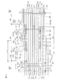
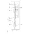
- FIG. 1 is a plan view of an electronic component module in which the electronic component according to the first embodiment of the present invention is incorporated.
- FIG. 2 is a view showing the connection form of the electronic component module and the potential of each part.
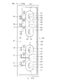
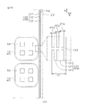
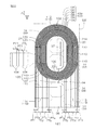
- FIG. 3 is a view for explaining a planar structure of the electronic component.
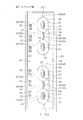
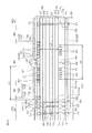
- FIG. 4 is a view for explaining a planar structure of the lower coil of the electronic component.
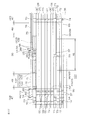
- FIG. 5 is a view for explaining a planar structure of the upper coil of the electronic component.
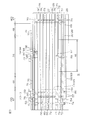
- 6 is a cross-sectional view taken along the line VI-VI in FIG. 7 is a cross-sectional view taken along the line VII-VII in FIG.
- FIG. 8 is a cross-sectional view showing a configuration of a comparative embodiment of the electronic component.
- FIG. 1 is a plan view of an electronic component module in which the electronic component according to the first embodiment of the present invention is incorporated.
- FIG. 2 is a view showing the connection form of the electronic component module and the potential of each part.
- FIG. 9 is a cross-sectional view taken along the line IX-IX in FIG.
- FIG. 10 is a graph comparing the average breakdown voltage of the electronic component according to the comparative embodiment of the present invention and the average breakdown voltage of the electronic component according to the first embodiment of the present invention.
- FIG. 11 is a graph comparing the variation in dielectric breakdown voltage of the electronic component according to the comparative embodiment of the present invention and the variation in dielectric breakdown voltage of the electronic component according to the first embodiment of the present invention.
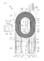
- FIG. 12 is a view for explaining a planar structure of the upper coil of the electronic component according to the second embodiment of the present invention.
- FIG. 13 is an enlarged view of a region XIII shown in FIG.
- FIG. 14 is an enlarged view of a region XIV shown in FIG. FIG.
- FIG. 15 is an enlarged view of a region XV shown in FIG.
- FIG. 16 is a cross-sectional view taken along the line XVI-XVI shown in FIG.
- FIG. 17 is a cross-sectional view taken along the line XVII-XVII shown in FIG.
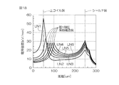
- FIG. 18 is a graph showing the relationship between the amount of extension of the first breakdown voltage holding structure and the electric field strength by simulation.
- FIG. 19 is a graph showing the relationship between the number of second dummy conductor patterns and the electric field strength by simulation.
- FIG. 20 is a graph comparing the average dielectric breakdown voltage of the electronic component according to the reference example of the present invention and the average dielectric breakdown voltage of the electronic component according to the second embodiment of the present invention.
- FIG. 21 is a view of a portion corresponding to FIG. 16 and is a cross-sectional view of the electronic component according to the third embodiment of the present invention.
- FIG. 22 is a view corresponding to FIG. 14 and is a view for explaining a planar structure on the first upper coil side of the electronic component according to the fourth embodiment of the present invention.
- FIG. 23 is a plan view showing the upper coil of the sample of the electronic component shown in FIG.
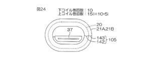
- FIG. 24 is a plan view showing the upper coil of the sample of the electronic component shown in FIG.
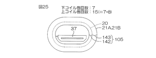
- FIG. 25 is a plan view showing the upper coil of the sample of the electronic component shown in FIG.
- FIG. 26 is a graph showing the measurement results of the electric field strength of the sample shown in FIG. 23, the sample shown in FIG. 24, and the sample shown in FIG.
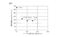
- FIG. 27 shows the average breakdown voltage of the electronic component according to the reference example of the present invention, the average breakdown voltage of the sample shown in FIG. 23, the average breakdown voltage of the sample shown in FIG. 24, and the average of the sample shown in FIG. It is the graph which compared the dielectric breakdown voltage.
- FIG. 28 is a cross-sectional view for explaining an electronic component according to the fifth embodiment of the present invention.
- FIG. 29 is a diagram for explaining the effect of the electronic component shown in FIG.
- FIG. 30 is a diagram for explaining the effect of the electronic component shown in FIG.
- FIG. 31 is a view for explaining a planar structure of the electronic component according to the sixth embodiment of the present invention.
- FIG. 32 is a view for explaining a planar structure of the low voltage side capacitor conductor film of the electronic component shown in FIG. FIG.
- FIG. 33 is a view for explaining a planar structure of the high voltage side capacitor conductor film of the electronic component shown in FIG. 31.
- FIG. 34 is a cross-sectional view taken along the line XXXIV-XXXIV shown in FIG.
- FIG. 35 is a cross-sectional view for explaining an electronic component according to the seventh embodiment of the present invention.
- FIG. 36 is a view showing a modification of the resin film pattern.
- FIG. 37 is a view showing a modification of the resin film pattern.
- FIG. 38 is a plan view of an electronic component module according to a modification.
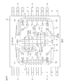
- FIG. 1 is a plan view of an electronic component module 1 in which the electronic component according to the first embodiment of the present invention is incorporated.
- the central portion of the electronic component module 1 is shown through for clarity of the internal structure.
- a high voltage pad electrically connected to the high voltage coil and a low voltage pad electrically connected to the low voltage coil may be laterally spaced apart on the surface of the electronic component.
- the distance between the low voltage pad and the high voltage pad is set to several tens of times or more as compared with the distance between the high voltage coil and the low voltage coil of the transformer from the viewpoint of securing a sufficient withstand voltage. For this reason, sufficient improvement has not been made to the point of improving the withstand voltage by utilizing the region between the low voltage pad and the high voltage pad.
- an electronic component and an electronic component module capable of improving the breakdown voltage are provided, focusing on the region between the low voltage pad and the high voltage pad.
- the package type of the electronic component module 1 is SOP (Small Outline Package).
- the package type of the electronic component module 1 is not limited to SOP, and various types such as QFP (Quad Flat Package) and SOJ (Small Outline J-lead Package) may be adopted.
- the electronic component module 1 is a power module in which a plurality of chips are integrated into one package.
- a resin package 2, a plurality of leads 3, and a plurality of chips 4 are included.
- the resin package 2 is formed in a square (square) plate shape using, for example, an epoxy resin.
- the plurality of leads 3 are provided across the inside and outside of the resin package 2 via a pair of opposing end surfaces of the resin package 2.
- the plurality of chips 4 includes a controller chip 5 (controller IC) as an example of a low voltage element, an electronic component 6, and a driver chip 7 (driver IC) as an example of a high voltage element.
- the electronic component 6 is, in this form, a transformer chip including a transformer.
- Each of the chips 5 to 7 is formed in a square (rectangular) plate shape.
- the size of the controller chip 5 and the size of the driver chip 7 may be approximately equal.
- the size of the electronic component 6 may be smaller than the controller chip 5 and the driver chip 7.
- the electronic component 6 is disposed substantially at the center of the resin package 2.
- the controller chip 5 and the driver chip 7 are disposed on one lead 3 side and the opposite lead 3 side of the electronic component 6, respectively.
- the controller chip 5 and the driver chip 7 are disposed so as to sandwich the electronic component 6 therebetween.
- the controller chip 5 and the driver chip 7 are respectively adjacent to the leads 3.
- the controller chip 5 and the electronic component 6 are disposed on the common first die pad 8.
- the driver chip 7 is disposed on a second die pad 9 spaced from the first die pad 8.
- a plurality of pads 10 and a plurality of pads 11 are formed on the surface of the controller chip 5.
- the plurality of pads 10 are arranged along the long side closer to the lead 3 of the controller chip 5.
- the plurality of pads 10 are connected to the leads 3 by bonding wires 12.
- the plurality of pads 11 are arranged along the long side opposite to the lead 3 of the controller chip 5 (closer to the electronic component 6).
- a plurality of low voltage pads 13 and a plurality of high voltage pads 14 are formed on the surface of the electronic component 6.
- the plurality of low voltage pads 13 are arranged along the long side of the electronic component 6 closer to the controller chip 5.
- the plurality of low voltage pads 13 are connected to the pads 11 of the controller chip 5 by bonding wires 15.
- the pad 11 of the controller chip 5 is connected to the primary side of the electronic component 6.
- the plurality of high voltage pads 14 are arranged along the long side of the electronic component 6 at the center in the width direction of the electronic component 6.
- a plurality of pads 16 and a plurality of pads 17 are formed on the surface of the driver chip 7.
- the plurality of pads 16 are arranged along the long side closer to the electronic component 6 of the driver chip 7.
- the plurality of pads 16 are connected to the high voltage pads 14 of the electronic component 6 by bonding wires 18.
- the pads 16 of the driver chip 7 are connected to the secondary side of the electronic component 6.
- the plurality of pads 17 are arranged along the long side of the driver chip 7 on the opposite side (closer to the lead 3) of the electronic component 6.
- the plurality of pads 17 are connected to the leads 3 by bonding wires 19.
- the arrangement of the pads of the chips 5 to 7 shown in FIG. 1 is merely an example, and can be appropriately changed according to the package type and the arrangement of the chips 4.
- FIG. 2 is a diagram showing the connection form of the electronic component module 1 of FIG. 1 and the potential of each part.
- the lower coil 20 is formed as an example of a low voltage coil (low voltage conductor pattern).
- the upper coil 21 is formed as an example of a high voltage coil (high voltage conductor pattern).
- the lower coil 20 and the upper coil 21 are each formed in a spiral shape.
- the magnetic coupling of the lower coil 20 and the upper coil 21 forms a transformer (a first transformer 301 and a second transformer 302 described later).
- the controller chip 5 and the driver chip 7 are DC-isolated by a transformer (lower coil 20 and upper coil 21).
- the controller chip 5 and the driver chip 7 are AC-connected by a transformer (lower coil 20 and upper coil 21).
- a low voltage wire 24 and a low voltage wire 93 are connected to the inner coil end 22 (the inner end of the spiral) and the outer coil end 92 (the outer end of the spiral) of the lower coil 20, respectively.
- the ends of the low voltage interconnections 24 and 93 are exposed as low voltage pads 13.
- a high voltage wire 25 (inner coil end wire) and a high voltage wire 95 (outer coil end wire) are connected to the inner coil end 23 and the outer coil end 94 of the upper coil 21, respectively.
- the ends of the high voltage lines 25 and 95 are exposed as high voltage pads 14.
- the controller chip 5 includes transistors Tr1 and Tr2.
- the transistors Tr ⁇ b> 1 and Tr ⁇ b> 2 are switching elements for conducting and blocking the wires 90 and 91, respectively.
- the transistor Tr1 is provided in the middle of a wire 90 connecting a certain pad 10 and a certain pad 11.
- the transistor Tr2 is provided in the middle of the wiring 91 connecting the other pad 10 and the other pad 11.
- the pads 10 and 11 on the side of the wiring 90 are connected to the input voltage and the low voltage pad 13 on the side of the outer coil end 92 through the bonding wires 12 and 15, respectively.
- the pads 10 and 11 on the side of the wiring 91 are connected to the ground voltage and the low voltage pad 13 on the side of the inner coil end 22 through the bonding wires 12 and 15, respectively.
- the lower coil 20 of the electronic component 6 is controlled by controlling the controller chip 5 so that the first application state (Tr1: ON, Tr2: OFF) and the second application state (Tr1: OFF, Tr2: ON) are alternately repeated.
- the alternating current signal to be transmitted is boosted according to the transformation ratio between the lower coil 20 and the upper coil 21.
- the transmitted AC signal is output to the driver chip 7 through the bonding wire 18.
- the reference voltage is output to the driver chip 7 set to 1200V.
- the specific voltage values shown in FIG. 2 are merely an example used to explain the operation of the electronic component module 1.
- the reference voltage of the driver chip 7 (HV region) may have a value exceeding 1200V.
- FIG. 3 is a view for explaining a planar structure of the electronic component 6 of FIG.
- FIG. 4 is a view for explaining the planar structure of the layer in which the lower coil 20 of the electronic component 6 is disposed.
- FIG. 5 is a view for explaining the planar structure of the layer in which the upper coil 21 of the electronic component 6 is disposed.
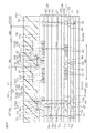
- FIG. 6 is a cross-sectional view of the electronic component 6 (a cross-sectional view taken along the line VI-VI in FIG. 3).
- FIG. 7 is a cross-sectional view of the electronic component 6 (a cross-sectional view along the line VII-VII in FIG. 3).
- FIGS. 6 and 7 only the metal parts are hatched for the sake of clarity.
- electronic component 6 includes a first transformer 301 and a second transformer 302.
- the first transformer 301 and the second transformer 302 are formed at intervals along the longitudinal direction of the electronic component 6.
- the first transformer 301 is shown at the top and the second transformer 302 is shown at the bottom.
- the first transformer 301 includes a pair of lower coil 20 and two upper coils 21 facing each other, as described later.
- the second transformer 302 also includes a pair of lower coil 20 and two upper coils 21 facing each other.
- the semiconductor substrate 26 and the insulating layer stack structure 27 formed on the semiconductor substrate 26 are included.
- a silicon (Si) substrate, a silicon carbide (SiC) substrate, or the like can be used as the semiconductor substrate 26 .
- the electronic component 6 is formed as a semiconductor device by the semiconductor substrate 26. Therefore, the electronic component module 1 including the electronic component 6 is formed as a semiconductor module.
- the insulating layer stack structure 27 is composed of a plurality of (12 layers in FIGS. 6 and 7) insulating layers 28 stacked in order from the surface of the semiconductor substrate 26.
- Each of the plurality of insulating layers 28 has a laminated structure of the lower layer etching stopper film 29 and the upper layer interlayer insulating film 30 except for the lowermost insulating layer 28 in contact with the surface of the semiconductor substrate 26.
- the lowermost insulating layer 28 is formed only of the interlayer insulating film 30.
- a SiN film, a SiC film, a SiCN film or the like may be used.
- a SiO 2 film may be used.
- the lower coil 20 and the upper coil 21 are formed in different insulating layers 28 in the insulating layer laminated structure 27.
- the lower coil 20 and the upper coil 21 face each other with one or more insulating layers 28 interposed therebetween.
- the lower coil 20 is formed on the fourth insulating layer 28 from the semiconductor substrate 26.
- the upper coil 21 is formed as an eleventh insulating layer 28 with six insulating layers 28 interposed between the upper coil 21 and the lower coil 20.
- the lower coil 20 and the upper coil 21 are respectively surrounded by the inner regions 31 and 32 so that the inward regions 31 and 32 in a plan view elliptical shape are defined at the center. Is formed in an oval annular area surrounding the.
- the upper coil 21 is formed so that the upper surface thereof is flush with the upper surface of the insulating layer 28. Thereby, the upper coil 21 is in contact with the different insulating layers 28 on the side surface, the upper surface and the lower surface.
- the etching stopper film 29 and the interlayer insulating film 30 are in contact with the side surface of the upper coil 21.
- the insulating layer 28 formed on the upper side of the insulating layer 28 in which the upper coil 21 is embedded only the lower layer etching stopper film 29 is in contact with the upper surface of the upper coil 21.
- the upper interlayer insulating film 30 is in contact with the lower surface of the upper coil 21.
- the lower coil 20 is also formed so that the upper surface thereof is flush with the upper surface of the insulating layer 28 similarly to the upper coil 21.
- a high voltage pad layer 88 as an example of a high voltage conductive layer is provided on the surface of the insulating layer stack structure 27 (on the interlayer insulating film 30 of the uppermost insulating layer 28).
- a low voltage pad layer 89 as an example of the low voltage conductive layer is provided on the surface of the insulating layer stack structure 27 (on the interlayer insulating film 30 of the uppermost insulating layer 28).
- a protective film 75 as an example of a surface insulating film and a passivation film 76 are sequentially stacked on the entire surface of the insulating layer stack structure 27 so as to integrally cover them.
- Pad openings 79 and 78 are formed in these films 75 and 76, respectively.
- Pad openings 79 and 78 expose high voltage pad layer 88 and low voltage pad layer 89 as high voltage pad 14 and low voltage pad 13, respectively.
- the high voltage pad 14 is disposed in the central high voltage region (HV region) 36 in which the upper coil 21 is disposed in a plan view when the electronic component 6 is viewed from above along the laminating direction of the insulating layer lamination structure 27 There is.
- the high voltage region 36 includes a region of the insulating layer 28 in which the upper coil 21 is embedded, in which a wire having the same potential as the upper coil 21 and the upper coil 21 is formed, and a peripheral portion of the formation region.
- a total of four upper coils 21 are formed in pairs at intervals in the longitudinal direction of the electronic component 6.
- An inner coil end wire 37 and an outer coil end wire 96 are formed between the inner region 32 of the upper coil 21 of each pair and the adjacent upper coil 21 respectively.
- each upper coil 21 pair one upper coil 21 and the other upper coil 21 are electrically connected to each other by a common outer coil end wire 96 therebetween. Both upper coils 21, the outer coil end wires 96 between them, and the inner coil end wires 37 in each upper coil 21 are all at the same potential.
- the electric field from the upper coil 21, the inner coil end wire 37 or the outer coil end wire 96 is also applied to the inner region 32 of each upper coil 21 and the region between the upper coils 21 in each pair of upper coils 21.
- the high voltage region 36 is included as a range.
- the area overlapping the upper coils 21 and the inward area 32 of each upper coil 21 in the plan view of FIGS. 3 and 5 are an example of the high voltage coil formation areas.
- a region other than the formation region of the high voltage coil is a coil outer region 85 outside the upper coil 21.
- the regions other than the high voltage coil formation region include, for example, a region between the upper coils 21 (inter-coil region 50) in each pair of upper coils 21 and a region along the periphery of each upper coil 21 (coil peripheral region 99) .
- the region where the lower coil 20 (low voltage coil) is disposed coincides with the high voltage region 36 in plan view, but is separated from the upper coil 21 (high voltage coil) by the plurality of insulating layers 28.
- the region where the lower coil 20 (low voltage coil) is disposed is not included in the high voltage region 36 referred to in this embodiment because the effect of the electric field from the upper coil 21 hardly affects.
- a total of six high voltage pads 14 are disposed above the inward region 32 of each upper coil 21 and above the inter-coil region 50 in each upper coil 21 pair. .
- the high voltage pads 14 may include a first pad 33 and a second pad 34.
- the first pad 33 is disposed above the inner region 32 of each upper coil 21.
- the first pad 33 faces the inward region 32 in the thickness direction (stacking direction) of the insulating layer stack structure 27.
- the second pads 34 are disposed above the inter-coil regions 50.
- the second pad 34 faces the inter-coil region 50 in the thickness direction (stacking direction) of the insulating layer stack structure 27.
- the first pad 33 is connected to the inner coil end wiring 37 embedded in the same insulating layer 28 as the upper coil 21 through the via 38.
- the second pad 34 is connected to the outer coil end wiring 96 embedded in the same insulating layer 28 as the upper coil 21 through the via 35 by the same structure. ing.
- the AC signal transmitted to the upper coil 21 can be output from the high voltage pad 14 through the inner coil end wire 37 and the via 38, and the outer coil end wire 96 and the via 35.
- the insulating layer stack structure 27 includes a low voltage region 46 (FIGS. 6 and 7) and an outer low voltage region 47 (FIG. 3) as low potential regions (LV regions) electrically isolated from the high voltage region 36. 7) and an intermediate region 48 (FIGS. 3 to 7) are set.
- the low voltage region 46 includes a region of the insulating layer 28 in which the lower coil 20 is embedded, in which a wire having the same potential as the lower coil 20 and the lower coil 20 is formed, and a peripheral portion of the formation region.
- the low voltage region 46 faces the high voltage region 36 with one or more insulating layers 28 interposed therebetween, as in the relationship between the lower coil 20 and the upper coil 21.
- the lower coil 20 is formed at a position facing the upper coil 21, that is, a total of four pairs of two at a distance in the longitudinal direction of the electronic component 6.
- An inner coil end wire 49 and an outer coil end wire 97 are formed between the inner region 31 of the lower coil 20 of each pair and the adjacent lower coil 20, respectively.
- each pair one lower coil 20 and the other lower coil 20 are electrically connected to each other by a common outer coil end wire 97 therebetween. Both lower coils 20, the outer coil end wires 97 between them, and the inner coil end wires 49 in each lower coil 20 are all at the same potential.
- the inner region 31 of each lower coil 20 and the region between the lower coils 20 in each pair are also within the range to which the electric field from the lower coil 20, the inner coil end wire 49 or the outer coil end wire 97 is applied.
- the low voltage region 46 is included.
- the inner coil end wiring 49 is disposed at a position shifted from the inner coil end wiring 37 on the high voltage side in plan view.
- the outer low voltage region 47 is set to surround the high voltage region 36 and the low voltage region 46, as shown in FIGS.
- Intermediate region 48 is set between high voltage region 36 and low voltage region 46 and outer low voltage region 47.
- the low voltage pad 13 is formed on the surface of the insulating layer stack structure 27 (on the interlayer insulating film 30 of the uppermost insulating layer 28) in the outer low voltage region 47. There is.
- the outer low voltage region 47 includes a first region 39 as an example of a first space and a second region 40 as an example of a second space.
- the first region 39 is a region on one side (left side in the drawing) with the high voltage pad 14 interposed therebetween.
- the second region 40 is a region on the other side (right side in the drawing) with the high voltage pad 14 interposed therebetween.
- the low voltage pad 13 is selectively biased to the first region 39.
- a total of six low voltage pads 13 are provided on each side of the high voltage pads 14 provided at intervals in the longitudinal direction of the electronic component 6 in the first region 39. It is arranged.
- Each low voltage pad 13 is connected to the lower coil 20 by low voltage wires 24 and 93 routed in the insulating layer stack structure 27.
- Low voltage interconnection 24 includes through interconnection 51 and lead interconnection 52.
- the through wiring 51 is formed in a columnar shape reaching the insulating layer 28 below the lower coil 20 through the insulating layer 28 in which at least the lower coil 20 is formed from each low voltage pad 13 in the outer low voltage region 47 There is.
- interconnection 51 includes low voltage layer interconnections 53 and 54 (low voltage interconnections) and vias 55, 56 and 57.
- the low voltage layer wirings 53 and 54 are respectively embedded in the same insulating layer 28 as the upper coil 21 and the lower coil 20 in an island shape (square shape).
- the plurality of vias 55 connect between the low voltage layer wirings 53 and 54.
- the via 56 connects the upper low voltage layer wiring 53 and the low voltage pad 13.
- the via 57 connects the lower low voltage layer wire 54 and the lead wire 52 to each other.
- the lead wire 52 is formed in a linear shape drawn from the low voltage region 46 to the outer low voltage region 47 via the insulating layer 28 below the lower coil 20.
- the lead wire 52 includes an inner coil end wire 49, a lead layer wire 58, and a via 59.
- the lead layer wiring 58 is linearly embedded in the insulating layer 28 below the lower coil 20.
- the extraction layer wire 58 crosses below the lower coil 20.
- the via 59 connects the lead layer wiring 58 and the inner coil end wiring 49.
- the lead layer wiring 58 is connected to the semiconductor substrate 26 through the via 86. Thereby, the low voltage wiring 24 is fixed to the substrate voltage (for example, the ground voltage).
- the low voltage wiring 93 is also constituted by the wiring including the through wiring 43 (FIG. 7) and the lead wiring 98 (FIGS. 3 to 5), similarly to the low voltage wiring 24.
- the first pad 41 disposed to the side of the first pad 33 of the high voltage pad 14 is a through wire 51 and a through wire 51 as shown in FIGS. It is connected to the inner coil end wire 49 of the lower coil 20 through the lead wire 52.
- the second pad 42 disposed on the side of the second pad 34 of the high voltage pad 14 has the outer coil end of the lower coil 20 through the through wire 43 and the lead wire 98. It is connected to the wiring 97.
- the signal input to the low voltage pad 13 can be transmitted to the lower coil 20 through the through wires 51 and 43 and the lead wires 52 and 98.
- a shield layer 69 is formed further outside than the low voltage wires 24, 93.
- the shield layer 69 prevents moisture from entering the device from the outside, and prevents cracks on the end face from spreading to the inside.
- the shield layer 69 is formed in a wall shape along the end face of the electronic component 6, as shown in FIGS.
- the bottom of the shield layer 69 is connected to the semiconductor substrate 26. Thereby, the shield layer 69 is fixed to the substrate voltage (for example, the ground voltage).
- shield layer 69 is formed of shield layer wiring 70 embedded in the same insulating layer 28 as upper coil 21, lower coil 20 and lead layer wiring 58, respectively. 72, a plurality of vias 73 connecting them, and a via 74 connecting the lowermost shield layer wiring 72 and the semiconductor substrate 26.
- a resin film 77 is formed on the protective film 75 and the passivation film 76 on the insulating layer stack structure 27.
- the resin film 77 is selectively formed on the passivation film 76 so as to integrally cover the entire high voltage region 36.
- the resin film 77 covers the region overlapping with each upper coil 21, the inward region 32 of each upper coil 21, the inter-coil region 50, and the coil peripheral region 99 in plan view of FIG. 3. Thereby, the resin film 77 covers the entire circumference of both the first pad 33 and the second pad 34 of the high voltage pad 14 in plan view.
- An opening for exposing the high voltage pad 14 in the resin film 77 corresponds to the pad opening 79.
- the resin film 77 has overlapping portions 44 and 45 that run on the peripheries of the first pad 33 and the second pad 34 of the high voltage pad 14.
- the protective film 75 is made of, for example, SiO 2 and has a thickness of about 150 nm.
- the passivation film 76 is made of, for example, SiN, and has a thickness of about 1000 nm.
- the resin film 77 is made of, for example, polyimide and has a thickness of about 4000 nm.
- a large potential difference (for example, about 1200 V) occurs between the lower coil 20 and the upper coil 21 of the electronic component 6.
- the insulating layer 28 disposed between the lower coil 20 and the upper coil 21 has a thickness capable of achieving a withstand voltage that does not cause dielectric breakdown due to a potential difference therebetween.
- the insulating layer 28 is made to interpose a plurality of layers (for example, six layers) between coils.
- the insulating layer 28 has a laminated structure of an etching stopper film 29 of about 300 nm and an interlayer insulating film 30 of about 2100 nm.
- the distance L1 between the high voltage pad 14 and the low voltage pad 13 is larger than the total thickness L2 of the insulating layer 28 between the lower coil 20 and the upper coil 21.
- the distance L1 is generally 100 ⁇ m or more and 450 ⁇ m or less, and is 6/1 or more and 40/1 or less in terms of the ratio to the thickness L2 (distance L1 / thickness L2).
- FIG. 8 is a cross-sectional view showing the configuration of the electronic component 6 according to the comparative embodiment of the present invention.
- FIG. 9 is a cross-sectional view taken along the line IX-IX in FIG. As shown in FIGS. 8 and 9, in the electronic component 6 according to the comparative embodiment, the resin film 77 exposes the periphery of the second pad 34 of the high voltage pad 14.
- FIG. 10 is a graph comparing the average breakdown voltage of the electronic component according to the comparative embodiment of the present invention and the average breakdown voltage of the electronic component 6 according to the first embodiment of the present invention.
- the vertical axis represents the average breakdown voltage [kVrms].
- the average breakdown voltage of the electronic component 6 according to the first embodiment is increased by 7.5% with respect to the average breakdown voltage of the electronic component 6 according to the comparative embodiment. From this, it was found that by covering the periphery of the second pad 34 with the resin film 77, the average dielectric breakdown voltage can be improved.
- FIG. 11 is a graph comparing the variation in dielectric breakdown voltage of the electronic component 6 according to the comparative embodiment of the present invention and the variation in dielectric breakdown voltage of the electronic component 6 according to the first embodiment of the present invention.
- the vertical axis represents the variation of the average breakdown voltage.
- the variation of the dielectric breakdown voltage of the electronic component 6 according to the first embodiment is reduced by 27.9% with respect to the variation of the dielectric breakdown voltage of the electronic component 6 according to the comparative embodiment. From this, it was found that the variation in the dielectric breakdown voltage can be suppressed by covering the periphery of the second pad 34 with the resin film 77.
- FIG. 12 is a view for explaining a planar structure of the upper coil 21 of the electronic component 101 according to the second embodiment of the present invention.
- the structure corresponding to the structure of the electronic component 6 is assigned the same reference numeral and the description is omitted.
- the high voltage portion is between the low voltage portion Form an electric field. Therefore, a relatively high electric field tends to concentrate on the high voltage part.
- the high voltage coils form an electric field with the low voltage coils. Therefore, a relatively high electric field tends to be concentrated on the high voltage coil. The occurrence of such electric field concentration may be a drawback in improving the withstand voltage.
- the structure of the first transformer 301 will be described as an example.
- the structure on the second transformer 302 side is the same as the structure on the first transformer 301 side, so the same reference numerals are given and the description is omitted.
- one upper coil 21 of the two upper coils 21 is referred to as a first upper coil 21A, and the other upper coil 21 is referred to as a second upper coil 21B, as necessary.
- first upper coil 21A the upper coil 21A
- second upper coil 21B the upper coil 21B
- first direction A the opposing direction of the first upper coil 21A and the second upper coil 21B
- second direction B the intersecting direction intersecting the first direction A
- second direction B is an orthogonal direction orthogonal to the first direction A.
- electronic component 101 is a transformer chip including a transformer in this form.
- the electronic component 101 includes a conductive pressure resistant holding structure 102.
- the withstand voltage holding structure 102 is formed in the region between the low voltage side member and the high voltage side member.
- the low voltage side member includes, for example, a low voltage pad 13 and a shield layer 69 fixed to a reference potential or a ground potential.
- the high voltage side member includes, for example, high voltage pad 14 and upper coils 21A, 21 and the like.
- the breakdown voltage holding structure 102 suppresses breakdown voltage deterioration caused by the electric field formed in the region between the low voltage side member and the high voltage side member.
- the breakdown voltage holding structure 102 includes a first breakdown voltage holding structure 103 on the high voltage side and a second breakdown voltage holding structure 104 on the low voltage side.
- the first withstand pressure holding structure 103 and the second withstand pressure holding structure 104 are shown in a simplified manner.
- the first withstand pressure holding structure 103 is formed along the upper coils 21A and 21B.
- the first withstand pressure holding structure 103 surrounds the upper coils 21A and 21B so as to partition the upper coils 21A and 21B from other regions.
- the first withstand voltage holding structure 103 collectively surrounds the upper coils 21A and 21B and the outer coil end wiring 96 formed between the upper coils 21A and 21B. That is, the first withstand pressure holding structure 103 is formed in a ring shape (elliptical ring shape) in a plan view.
- the second withstand voltage holding structure 104 is formed in a region between the upper coils 21A and 21B and the low voltage layer wiring 53 (low voltage pad 13) in plan view.
- the second withstand pressure holding structure 104 extends in a line along the first direction A.
- the second withstand voltage holding structure 104 is formed along the plurality of low voltage layer wires 53 (low voltage pads 13) in plan view. Thus, the second withstand voltage holding structure 104 protrudes outward beyond the outer contour of the low voltage pad 13 in plan view.
- the second withstand voltage holding structure 104 extends in a line along the first direction A so as to cross the plurality of low voltage pads 13. Thus, the second withstand voltage holding structure 104 divides the upper coils 21A and 21B from the plurality of low voltage pads 13 (low voltage layer wires 53).
- FIG. 13 is an enlarged view of a region XIII shown in FIG.
- FIG. 14 is an enlarged view of a region XIV shown in FIG.
- FIG. 15 is an enlarged view of a region XV shown in FIG.
- FIG. 16 is a cross-sectional view taken along the line XVI-XVI shown in FIG.
- FIG. 17 is a cross-sectional view taken along the line XVII-XVII shown in FIG.
- the outlines of the upper coils 21A and 21B are shown by thick lines.
- the outer contours of the upper coils 21A and 21B are respectively formed by the outer peripheral edge of the spiral pattern 105 for one turn that forms the outermost periphery of the upper coils 21A and 21B.
- the outline of the lower coil 20 is shown by a broken line.
- the outer shell of the lower coil 20 is formed by the outer peripheral edge of a spiral pattern of one turn that forms the outermost periphery of the lower coil 20.
- the first pad 33 and the second pad 34 of the high voltage pad 14 are respectively shown by broken lines.
- upper coils 21A and 21B include inner coil end 22, outer coil end 94 and spiral pattern 105, respectively.
- the inner coil ends 22 of the upper coils 21A and 21B are respectively formed in a region surrounded by the outer shell of the lower coil 20 in a plan view.
- the outer coil ends 94 of the upper coils 21A and 21B are respectively formed in an area outside the area surrounded by the outer shell of the lower coil 20 in a plan view.
- the spiral patterns 105 of the upper coils 21A and 21B are wound around the outer coil end 22 from the inner coil end 22 to the outer coil end 94, respectively.
- the number of turns of the spiral pattern 105 may be 5 or more and 30 or less (for example, 15).
- the width of the spiral pattern 105 may be 0.5 ⁇ m to 5 ⁇ m.
- the width of the spiral pattern 105 is preferably 1 ⁇ m or more and 3 ⁇ m or less.
- the width of the spiral pattern 105 is defined by the width in the direction orthogonal to the spiral direction.
- the winding pitch PTL of the spiral pattern 105 may be 0.1 ⁇ m to 10 ⁇ m.
- the winding pitch PTL of the spiral pattern 105 is preferably 1 ⁇ m or more and 3 ⁇ m or less.
- the winding pitch PTL of the spiral pattern 105 is defined by the distance between two spiral patterns 105 adjacent in the direction orthogonal to the spiral direction.
- the inner coil ends 22 of the upper coils 21A and 21B are connected to the inner coil end wiring 37 through the inner connection portion 106, respectively.
- the inner connection portions 106 are respectively drawn from the inner coil end wiring 37 toward the inner coil end 22.
- the outer coil ends 94 of the upper coils 21A and 21B are connected to the outer coil end wiring 96 through the outer connection portion 107, respectively.
- the outer connection portions 107 are respectively drawn from the outer coil end wiring 96 toward the outer coil end 94.
- the structure of the lower coil 20 is substantially the same as the structure of the upper coils 21A and 21B as described in the first embodiment. The specific description of the lower coil 20 is omitted.
- first breakdown voltage holding structure 103 is formed in the same insulating layer 28 (interlayer insulating film 30) as upper coils 21A and 21B.
- the first withstand pressure holding structure 103 is formed through a process common to the upper coils 21A and 21B. Therefore, the first withstand voltage holding structure 103 is formed of an electrode layer common to the upper coils 21A and 21B.
- the first pressure-resistant holding structure 103 is formed along the outer contours of the upper coils 21A and 21B so as to protrude outside the outer contour (see the broken line in FIG. 14) of the lower coil 20 in plan view.
- the first withstand pressure holding structure 103 is further formed along the outer contour of the second pad 34 so as to protrude outward beyond the outer contour of the second pad 34 (see the broken line in FIG. 14) in plan view.
- the first withstand pressure holding structure 103 collectively surrounds the upper coils 21A and 21B and the outer coil end wiring 96 formed between the upper coils 21A and 21B. That is, the first withstand pressure holding structure 103 is formed in a ring shape (elliptical ring shape) in a plan view. The first withstand voltage holding structure 103 divides the upper coil 21A, 21B and the outer coil end wire 96 formed between the upper coil 21A, 21B from the other region.
- the first withstand voltage holding structure 103 includes a first dummy conductor pattern group 109 formed by an assembly of a plurality (for example, six) of first dummy conductor patterns 108. In FIG. 16 and FIG. 17, a part of the first dummy conductor pattern group 109 is omitted.
- Each of the plurality of first dummy conductor patterns 108 has a discontinuous pattern with respect to the spiral pattern 105 of the upper coils 21A and 21B.
- the plurality of first dummy conductor patterns 108 are formed at intervals along the direction away from the upper coils 21A and 21B.
- the first dummy conductor patterns 108 collectively surround the upper coils 21A and 21B and the outer coil end wiring 96 formed between the upper coils 21A and 21B. That is, each first dummy conductor pattern 108 is formed in a ring shape (elliptical ring shape) in plan view.
- the width of the first dummy conductor pattern 108 may be 0.5 ⁇ m to 5 ⁇ m.
- the width of the first dummy conductor pattern 108 is preferably 1 ⁇ m to 3 ⁇ m.
- the width of the first dummy conductor pattern 108 may be equal to the width of the spiral pattern 105.
- the width of the first dummy conductor pattern 108 is defined by the width in the direction orthogonal to the direction in which the first dummy conductor pattern 108 extends.
- each first dummy conductor pattern 108 includes an open portion 110 in which no electrode layer is present.
- the open portion 110 of each first dummy conductor pattern 108 is formed by a part of the insulating layer 28 (the interlayer insulating film 30). Thereby, each first dummy conductor pattern 108 is formed in an end-like shape.
- the first dummy conductor pattern group 109 is located on the opposite side to the upper coils 21A and 21B with respect to the inner first dummy conductor pattern 108 located on the upper coils 21A and 21B and the inner first dummy conductor pattern 108.
- An outer first dummy conductor pattern 108 is included.
- the outer first dummy conductor pattern 108 extends so as to close the open portion 110 of the inner first dummy conductor pattern 108 from the outside.
- the open portion 110 of the outer first dummy conductor pattern 108 is formed in a region different from the open portion 110 of the inner first dummy conductor pattern 108.
- An open circuit including the first dummy conductor pattern 108 is formed by the open portion 110. That is, the open portion 110 prevents the current path from being formed in the first dummy conductor pattern 108.
- At least one or all of the plurality of first dummy conductor patterns 108 may be endless.
- Each first dummy conductor pattern 108 is connected to the outer coil end wiring 96 via the first dummy connection portion 111. Thereby, each first dummy conductor pattern 108 is fixed at the same potential as the outer coil end 94 of the upper coils 21A and 21B.
- the first dummy connection portion 111 is drawn from the outer coil end wiring 96 along an arbitrary direction.
- the first dummy connection portion 111 may be drawn from a region different from the outer connection portion 107.
- the first dummy connection portion 111 is drawn along the second direction B from a region different from the outer connection portion 107.
- the first withstand voltage holding structure 103 includes a first proximity region 112, a second proximity region 113, a first connection region 114, and a second connection region 115.
- the first proximity region 112, the second proximity region 113, the first connection region 114, and the second connection region 115 are each formed by a first dummy conductor pattern group 109.
- the first proximity region 112 is in proximity to the first upper coil 21A, and extends in a U-shape along the outer contour of the first upper coil 21A.
- the first proximity region 112 sandwiches the first upper coil 21A from three directions.
- the first proximity region 112 divides the first upper coil 21A from the low voltage pad 13 (low voltage layer wiring 53) and the shield layer 69.
- the second adjacent region 113 is adjacent to the second upper coil 21B, and extends in a U-shape along the outer contour of the second upper coil 21B.
- the second proximity region 113 sandwiches the second upper coil 21B from three directions.
- the second proximity region 113 divides the second upper coil 21 B from the low voltage pad 13 (low voltage layer wiring 53) and the shield layer 69.
- the first connection region 114 is formed in a line extending in the first direction A in a region on the low voltage pad 13 side with respect to the outer coil end wiring 96.
- the first connection region 114 connects one end of the first proximity region 112 and one end of the second proximity region 113.
- the first connection region 114 divides a part of the upper coils 21A and 21B and the outer coil end wiring 96 from the low voltage pad 13 (low voltage layer wiring 53).
- first connection region 114 is formed along the outline of the second pad 34 (see the broken line in FIG. 14) in the region on the low voltage pad 13 side with respect to the outer coil end wire 96 .
- the plurality of first dummy conductor patterns 108 included in the first connection region 114 are formed at intervals along the direction away from the second pad 34.
- the direction away from the second pad 34 is the second direction B.
- the second connection region 115 is formed in a line extending in the first direction A in a region opposite to the first connection region 114 with respect to the outer coil end wiring 96.
- the second connection region 115 connects the other end of the first proximity region 112 and the other end of the second proximity region 113.
- the second connection region 115 defines a part of the upper coils 21A and 21B and the outer coil end wiring 96 from the shield layer 69.
- the second connection region 115 extends along the outline of the second pad 34 (see the broken line in FIG. 14) in the region opposite to the first connection region 114 with respect to the outer coil end wire 96. It is formed.
- the plurality of first dummy conductor patterns 108 included in the second connection region 115 are formed at intervals along the direction away from the second pad 34.
- the direction away from the second pad 34 is the second direction B.
- the plurality of first dummy conductor patterns 108 included in the first proximity region 112 and the second proximity region 113 are each formed at a first pitch PT1.
- the first pitch PT1 is determined by the distance between the first dummy conductor pattern 108 closest to the upper coils 21A and 21B and the upper coils 21A and 21B and the distance between the two first dummy conductor patterns 108 adjacent to each other. It is defined.
- the plurality of first dummy conductor patterns 108 included in the first connection region 114 and the second connection region 115 are formed at the second pitches PTa, PTb, PTc, PTd, PTe, and PTf, respectively.
- the second pitch PTa is defined by the distance along the second direction B between the first dummy conductor pattern 108 and the second pad 34 closest to the second pad 34.
- the second pitches PTb to PTf are each defined by a distance along the second direction B between two adjacent first dummy conductor patterns 108 adjacent to each other.
- the second pitches PTa to PTf can take values different from the first pitch PT1 (PTa to PTf ⁇ PT1).
- the second pitches PTa to PTf may be 1 ⁇ m to 50 ⁇ m.
- the second pitches PTa to PTf can take various values in the range of 1 ⁇ m to 50 ⁇ m. The respective values of the second pitches PTa to PTf will be described in detail later.
- the overhang amount Z1 of the first withstand pressure holding structure 103 with respect to the outer shell of the lower coil 20 may be more than 0 ⁇ m and 100 ⁇ m or less (0 ⁇ m ⁇ Z1 ⁇ 100 ⁇ m).
- the overhang amount Z1 may be adjusted by changing the number of first dummy conductor patterns 108 or the value of the first pitch PT1.
- the insulating layer 28 may have a dielectric breakdown strength of 8 MV / cm or more and 10 MV / cm or less.
- the insulating layer 28 may contain at least one of SiO 2 or SiN.
- the overhang amount Z1 is preferably 10 ⁇ m or more. More specifically, the overhang amount Z1 is more preferably 20 ⁇ or more.
- the overhang amount Z1 is determined by the distance between the outer periphery of the lower coil 20 and the outer periphery of the first dummy conductor pattern 108 forming the outermost periphery of the first withstand voltage holding structure 103 in the first adjacent region 112 and the second adjacent region 113. It is defined.
- the resin package 2 may have a dielectric breakdown strength of 0.1 or more and 0.3 MV / cm or less.
- the resin package 2 may contain at least one mold resin of an epoxy resin, a polyimide resin, or a polybenzoxazole resin.
- the "breakdown strength" is defined by the maximum value of electric field strength that can be applied without causing breakdown (the same applies hereinafter).
- the first adjacent region 112 of the first withstand voltage holding structure 103 forms a first coil side withstand voltage holding structure 116 that suppresses a decrease in withstand voltage on the side of the first upper coil 21A. More specifically, the first coil side withstand voltage holding structure 116 suppresses the decrease in the withstand voltage caused by the electric field formed between the first upper coil 21A and the low voltage pad 13 (low voltage layer wiring 53). Further, the first coil side withstand voltage holding structure 116 suppresses the decrease in the withstand voltage caused by the electric field formed between the first upper coil 21A and the shield layer 69.
- the second adjacent region 113 of the first withstand voltage holding structure 103 forms a second coil side withstand voltage holding structure 117 that suppresses a decrease in withstand voltage on the second upper coil 21B side. More specifically, the second coil side withstand voltage holding structure 117 suppresses a decrease in withstand voltage caused by an electric field formed between the second upper coil 21B and the low voltage pad 13 (low voltage layer wiring 53). Further, the second coil side withstand voltage holding structure 117 suppresses the decrease in the withstand voltage caused by the electric field formed between the second upper coil 21 B and the shield layer 69.
- the first connection region 114 of the first breakdown voltage holding structure 103 forms a first pad-side breakdown voltage holding structure 118 that suppresses a decrease in breakdown voltage on the second pad 34 side. More specifically, the first pad side withstand voltage holding structure 118 suppresses the decrease in the withstand voltage caused by the electric field formed between the outer coil end wire 96 and the low voltage pad 13 (low voltage layer wire 53). In addition, the first pad side withstand voltage holding structure 118 suppresses the decrease in withstand voltage caused by the electric field formed between the second pad 34 and the shield layer 69.
- the second connection region 115 of the first breakdown voltage holding structure 103 forms a second pad-side breakdown voltage holding structure 119 which suppresses a drop in breakdown voltage on the second pad 34 side. More specifically, the second pad side withstand voltage holding structure 119 suppresses the decrease in withstand voltage caused by the electric field formed between the second pad 34 and the shield layer 69.
- the second withstand voltage holding structure 104 is formed in the same insulating layer 28 (interlayer insulating film 30) as the upper coils 21A and 21B.
- the second withstand voltage holding structure 104 is formed through a process common to the upper coils 21A and 21B. Therefore, the second withstand voltage holding structure 104 is formed of an electrode layer common to the upper coils 21A and 21B.
- the second withstand voltage holding structure 104 includes a second dummy conductor pattern group 122 formed by an assembly of a plurality (for example, three) of second dummy conductor patterns 121. In FIG. 16 and FIG. 17, a part of the second dummy conductor pattern group 122 is omitted. Each of the plurality of second dummy conductor patterns 121 has a discontinuous pattern with respect to the spiral pattern 105 of the upper coils 21A and 21B.
- Each of the plurality of second dummy conductor patterns 121 includes a linear pattern extending along the first direction A.
- the plurality of second dummy conductor patterns 121 are arranged at intervals along the second direction B.
- the width of the second dummy conductor pattern 121 may be 0.5 ⁇ m or more and 5 ⁇ m or less.
- the width of the second dummy conductor pattern 121 is preferably 1 ⁇ m or more and 3 ⁇ m or less.
- the width of the second dummy conductor pattern 121 may be equal to the width of the spiral pattern 105.
- the width of the second dummy conductor pattern 121 may be equal to the width of the first dummy conductor pattern 108.
- the width of the second dummy conductor pattern 121 is defined by the width in the direction orthogonal to the direction in which the second dummy conductor pattern 121 extends.
- the direction perpendicular to the direction in which the second dummy conductor patterns 121 extend is the second direction B.
- the plurality of second dummy conductor patterns 121 are each formed at the third pitch PT3.
- the third pitch PT3 is defined by the distance between the second dummy conductor pattern 121 closest to the low voltage pad 13 and the low voltage pad 13 and the distance between two adjacent second dummy conductor patterns 121 adjacent to each other. Ru.
- Each second dummy conductor pattern 121 is formed to have an end. Thus, an open circuit including the second dummy conductor pattern 121 is formed. That is, the open circuit prevents the current path from being formed in the second dummy conductor pattern 121.
- the generation of noise due to the second dummy conductor pattern 121 is suppressed.
- at least one or all of the plurality of second dummy conductor patterns 121 may be endless.
- Each second dummy conductor pattern 121 is connected to the low voltage layer wiring 53 via the second dummy connection portion 123. Thereby, each second dummy conductor pattern 121 is fixed to the same potential as the low voltage pad 13 (low voltage layer wiring 53).
- the second dummy connection portion 123 is drawn from an arbitrary low voltage layer wiring 53 toward the region on the upper coil 21A, 21B side.
- the second dummy connection portion 123 is drawn from the low voltage layer wire 53 corresponding to the outer coil end wire 97 of the lower coil 20 in this embodiment.
- the second dummy connection portion 123 is drawn in a line along the second direction B in this embodiment.
- One or more second dummy connections 123 may be drawn from one or more low voltage layer wires 53.
- the overhanging amount Z2 of the second withstand pressure holding structure 104 may be more than 0 ⁇ m and not more than 50 ⁇ m (0 ⁇ m ⁇ Z2 ⁇ 50 ⁇ m).
- the overhang amount Z2 of the second withstand voltage holding structure 104 is an outer periphery of the low voltage pad 13 and a peripheral edge on the upper coil 21A, 21B side of the second dummy conductor pattern 121 closest to the upper coil 21A, 21B in the second direction B. Defined by the distance between
- the second withstand voltage holding structure 104 suppresses the decrease in withstand voltage caused by the electric field formed between the first upper coil 21A and the low voltage pad 13 (low voltage layer wiring 53). Further, the second withstand voltage holding structure 104 suppresses a decrease in withstand voltage caused by an electric field formed between the second upper coil 21B and the low voltage pad 13 (low voltage layer wiring 53). Further, the second withstand voltage holding structure 104 suppresses the decrease in withstand voltage caused by the electric field formed between the second pad 34 and the low voltage pad 13 (low voltage layer wiring 53).
- the electric field strength includes the peak value of the electric field strength.
- first coil side withstand voltage holding structure 116 will be described as an example below, the same description applies to the second coil side withstand voltage holding structure 117. Therefore, the description regarding the first coil side withstand voltage holding structure 116 is applied to the description regarding the second coil side withstand voltage holding structure 117, and the description regarding the second coil side withstand voltage holding structure 117 is omitted.
- the first pad side withstand voltage holding structure 118 is described as an example, but the same description applies to the second pad side withstand voltage holding structure 119. Therefore, the description of the first pad-side breakdown voltage holding structure 118 is applied to the description of the second pad-side breakdown voltage holding structure 119, and the description of the second pad-side breakdown voltage holding structure 119 is omitted.
- the sample A1 is an electronic component according to a reference example.
- the electronic component according to the reference example has the same structure as the electronic component 101 according to the present embodiment except that the pressure-resistant holding structure 102 is not provided.
- the description of the structure of the electronic component according to the reference example is omitted (the same applies in the following).
- the sample B1 is the electronic component 101 in which the projection amount Z1 of the first withstand pressure holding structure 103 is set to 10 ⁇ m.
- the sample C1 is the electronic component 101 in which the projection amount Z1 of the first withstand pressure holding structure 103 is set to 20 ⁇ m.
- the sample D1 is the electronic component 101 in which the projection amount Z1 of the first withstand pressure holding structure 103 is set to 30 ⁇ m.
- the sample E1 is the electronic component 101 in which the projection amount Z1 of the first withstand pressure holding structure 103 is set to 40 ⁇ m.
- the sample F1 is the electronic component 101 in which the projection amount Z1 of the first withstand pressure holding structure 103 is set to 50 ⁇ m.
- FIG. 18 is a graph showing the relationship between the overhang amount Z1 of the first withstand voltage holding structure 103 and the electric field strength by simulation.
- the vertical axis represents electric field strength [kV / mm]
- the horizontal axis represents the distance [ ⁇ m] between the first withstand voltage holding structure 103 and the shield layer 69.
- the outer contour (outermost peripheral edge) of the upper coils 21A and 21B is simply referred to as “upper coil end”.
- the outer periphery (the outermost peripheral edge) of the first withstand pressure holding structure 103 is simply referred to as “the first withstand pressure holding structure end”.
- the inner periphery (inner peripheral edge) of the shield layer 69 is simply referred to as “shield layer end”.
- FIG. 18 shows a first curve LN1, a second curve LN2, a third curve LN3, a fourth curve LN4, a fifth curve LN5 and a sixth curve LN6.
- the first curve LN1 shows the simulation result of the sample A1.
- the second curve LN2 shows the simulation result of the sample B1.
- the third curve LN3 shows the simulation result of the sample C1.
- the fourth curve LN4 shows the simulation result of the sample D1.
- the fifth curve LN5 shows the simulation result of the sample E1.
- the sixth curve LN6 shows the simulation result of the sample F1.
- the electric field strength on the upper coil end side of the sample A1 was 56 kV / mm.
- the electric field strength at the end of the first withstand pressure holding structure of sample B1 was 34 kV / mm.
- the electric field strength at the end of the first withstand voltage holding structure of sample C1 was 28 kV / mm.
- the electric field strength at the end of the first withstand voltage holding structure of sample D1 was 28 kV / mm.
- the electric field strength at the end of the first withstand voltage holding structure of sample E1 was 28 kV / mm.
- the electric field strength at the end of the first withstand pressure holding structure of sample F1 was 28 kV / mm.
- the electric field strength at the upper coil end of sample A1 was higher than the electric field strength of samples B1 to F1. That is, in the sample A1 not having the first withstand voltage holding structure 103, the electric field concentration at the upper coil end was remarkable. On the other hand, in the samples B1 to F1 having the first withstand voltage holding structure 103, it was found that the electric field concentration at the upper coil end was relaxed.
- the electric field strength at the shield layer end of sample A1 was 20 kV / mm.
- the electric field strength at the shield layer end of sample B1 was 24 kV / mm.
- the electric field strength at the shield layer end of sample C1 was 26 kV / mm.
- the electric field strength at the shield layer end of sample D1 was 28 kV / mm.
- the electric field strength at the shield layer end of sample E1 was 29 kV / mm.
- the electric field strength at the shield layer end of sample F1 was 30 kV / mm.
- the electric field strength at the end of the shield layer increased in proportion to the increase of the overhang amount Z1 of the first withstand voltage holding structure 103. This is the result of meeting the physical law in which the electric field strength is inversely proportional to the distance.
- the overhang amount Z1 of the first withstand voltage holding structure 103 is not zero (that is, the overhang amount Z1> 0)
- the electric field concentration at the upper coil end is relaxed. It turned out that On the other hand, when the overhang amount Z1 of the first withstand pressure holding structure 103 exceeds 20 ⁇ m, the electric field strength at the end of the first withstand pressure holding structure settles to about 28 kV / mm.
- the electric field strength on the first withstand voltage holding structure 103 side is between the end of the first withstand voltage holding structure and the shield layer end. It turned out to be dominated by distance. This is one of the reasons why the electric field strength at the end of the shield layer is increased.
- the results of FIG. 18 are summarized below. It is preferable to provide the first withstand voltage holding structure 103 (the first coil side withstand voltage holding structure 116). Thus, the end of the electric field formed between the upper coils 21A and 21B and the lower coil 20 can be shifted from the upper coils 21A and 21B to the first withstand voltage holding structure 103 side.
- the first withstand pressure holding structure 103 protrudes outward from the outer shell of the upper coils 21A and 21B. Therefore, the electric field formed between the lower coil 20 and the upper coils 21A and 21B can be shielded by the first withstand pressure holding structure 103. As a result, the formation of an electric field can be suppressed so as to wrap around the end portions of the upper coils 21A and 21B.
- electric field concentration on the upper coils 21A and 21B can be alleviated. More specifically, in the region between the upper coils 21A and 21B and the low voltage pad 13, the electric field concentration on the upper coil end (the first withstand voltage holding structure end) can be alleviated. Further, in the region between the upper coils 21A and 21B and the shield layer 69, the concentration of the electric field on the upper coil end (the end of the first withstand voltage holding structure) can be alleviated.
- the overhang amount Z1 of the first withstand pressure holding structure 103 exceeds 0 ⁇ m. “The overhang amount Z1 exceeds 0 ⁇ m” is synonymous with the formation of the first dummy conductor pattern 108.
- the overhang amount Z1 of the first pressure-resistant structure 103 may be 10 ⁇ m or more and 50 ⁇ m or less.
- the electric field strength at the end of the first withstand voltage holding structure becomes 34 kV / mm or less, and the electric field concentration at the upper coil end can be alleviated.
- the absolute value of the difference between the electric field strength at the end of the first withstand voltage holding structure and the electric field strength at the end of the shield layer is 15 kV / mm or less.
- the overhang amount Z1 of the first withstand pressure holding structure 103 is preferably 20 ⁇ m or more and 50 ⁇ m or less.
- the electric field strength at the end of the first withstand voltage holding structure becomes 30 ⁇ m or less, and the electric field concentration at the upper coil end can be relaxed.
- the absolute value of the difference between the electric field strength at the end of the first withstand voltage holding structure and the electric field strength at the end of the shield layer is 5 kV / mm or less.
- Sample A2 is an electronic component according to a reference example.
- the sample B2 is an electronic component 101 including three second dummy conductor patterns 121.
- the sample C2 is an electronic component 101 including six second dummy conductor patterns 121.
- the sample D 2 is an electronic component 101 including twelve second dummy conductor patterns 121.
- FIG. 19 is a graph showing the relationship between the number of second dummy conductor patterns 121 and the electric field strength by simulation.
- the vertical axis represents electric field strength [kV / mm]
- the horizontal axis represents the number [pcs] of second dummy conductor patterns 121.
- the peripheral edge on the upper coil 21A, 21B side of the low voltage pad 13 is simply referred to as "low voltage pad end”.
- the peripheral edge on the upper coil 21A, 21B side of the second withstand pressure holding structure 104 is simply referred to as "the second withstand pressure holding structure end”.
- FIG. 19 shows a first plot point P1, a second plot point P2, a third plot point P3 and a fourth plot point P4.
- the first plot point P1 indicates the electric field strength at the low voltage pad end in the sample A2.
- the second plot point P2 indicates the electric field strength at the end of the second withstand voltage holding structure in the sample B2.
- the third plot point P3 indicates the electric field strength at the end of the second withstand voltage holding structure in the sample C2.
- the fourth plot point P4 indicates the electric field strength at the end of the second withstand voltage holding structure in the sample D2.
- the electric field strength at the low voltage pad end was 45 kV / mm.
- the electric field strength at the end of the second withstand pressure holding structure was 30 kV / mm.
- the electric field strength at the end of the second withstand voltage holding structure was 35 kV / mm.
- the electric field strength at the end of the second withstand voltage holding structure was 38 kV / mm.
- the electric field strength at the low voltage pad end of sample A2 was higher than the electric field strength at the end of the second withstand voltage holding structure of samples B2 to D2. That is, in the sample A2 not having the second withstand voltage holding structure end, the electric field concentration at the low voltage pad end was remarkable. On the other hand, it was found that in the samples B2 to D2 each having the second withstand voltage holding structure end, the electric field concentration to the low voltage pad end was relaxed.
- the electric field strength at the upper coil end was 25 kV / mm.
- the electric field strength at the upper coil end was 30 kV / mm.
- the electric field strength at the upper coil end was 31 kV / mm.
- the electric field strength at the end of the upper coil increased in proportion to the increase in the number of second dummy conductor patterns 121. This is the result of meeting the physical law in which the electric field strength is inversely proportional to the distance.
- the electric field concentration on the low voltage pad 13 is alleviated by forming the second breakdown voltage holding structure 104.
- the suppression effect of the electric field concentration on the low voltage pad 13 is not necessarily enhanced by the increase in the number of second dummy conductor patterns 121.
- the second withstand pressure holding structure 104 It is preferable to form the second withstand pressure holding structure 104. Thereby, in the region between the low voltage pad 13 and the upper coils 21A and 21B, the concentration of the electric field to the low voltage pad end (the second withstand voltage holding region end) can be alleviated. Further, in the region between the low voltage pad 13 and the second pad 34, the concentration of the electric field to the low voltage pad end (the second withstand voltage holding area end) can be alleviated.
- the overhanging amount Z2 of the second pressure-resistant holding structure 104 preferably exceeds 0 ⁇ m. “The overhang amount Z2 exceeds 0 ⁇ m” is substantially the same as forming the second dummy conductor pattern 121.
- the number of second dummy conductor patterns 121 may be twelve or less.
- the projecting amount Z2 of the second pressure-resistant holding structure 104 may be more than 0 ⁇ m and 50 ⁇ m or less.
- the electric field strength with respect to the second withstand voltage holding structure 104 is 35 kV / mm or less, and the electric field concentration with respect to the low voltage pad end (the second withstand voltage holding area end) can be relaxed.
- the absolute value of the difference between the electric field strength at the end of the second withstand voltage holding structure and the electric field strength at the upper coil end may be 10 kV / mm or less.
- the number of second dummy conductor patterns 121 may be six or less.
- the overhang amount Z2 of the second pressure-resistant holding structure 104 may be more than 0 ⁇ m and 25 ⁇ m or less.
- the electric field strength to the low voltage pad end is 35 kV / mm or less, and the electric field concentration to the low voltage pad end (the second withstand voltage holding area end) can be relaxed.
- the absolute value of the difference between the electric field strength at the end of the second withstand voltage holding structure and the electric field strength at the upper coil end may be 5 kV / mm or less.
- the number of second dummy conductor patterns 121 may be three or less.
- the projecting amount Z2 of the second pressure-resistant holding structure 104 may be more than 0 ⁇ m and 10 ⁇ m or less.
- the electric field strength with respect to the low voltage pad end is 30 kV / mm or less, and the electric field concentration with respect to the low voltage pad end (the second withstand voltage holding area end) can be relaxed.
- the absolute value of the difference between the electric field strength at the end of the second withstand voltage holding structure and the electric field strength at the upper coil end may be 5 kV / mm or less.
- first pad side breakdown voltage holding structure end the end on the low voltage pad 13 (low voltage layer wiring 53) side of the second pad 34 is simply referred to as a "second pad end”. Further, an end portion on the low voltage pad 13 (low voltage layer wiring 53) side of the first pad side breakdown voltage holding structure 118 (first breakdown voltage holding structure 103) is simply referred to as "first pad side breakdown voltage holding structure end”.
- the electric field strength of the first pad side withstand voltage holding structure end was determined for the samples A3 to C3.
- Table 3 also shows the electric field strength of the second pad end of the electronic component according to the reference example.
- the electric field strength at the end of the first pad side withstand voltage holding structure was 25 kV / mm.
- the electric field strength at the end of the first pad side withstand voltage holding structure was 9 kV / mm.
- the electric field strength at the end of the first pad side withstand voltage holding structure was 5 kV / mm.
- the second pitch PTa between the first dummy conductor pattern 108 closest to the second pad 34 and the second pad 34 is preferably equal to or less than the second pitch PTb to PTf.
- the second pitch PTa is preferably equal to or less than the longitudinal distance L2 (PTa ⁇ L2) between the upper coils 21A and 21B and the lower coil 20.
- the longitudinal distance L2 is a total thickness L2 of the insulating layer 28 between the lower coil 20 and the upper coil 21.
- the second pitch PTa closest to the second pad 34 is preferably 10 ⁇ m or less (PTa ⁇ 10 ⁇ m). As a result, the electric field strength at the end of the first pad side withstand voltage holding structure becomes 10 kV / mm or less, and the electric field strength at the second pad end can be effectively reduced.
- the second pitches PTa to PTf of the first pad side withstand voltage holding structure 118 do not necessarily have to be set to the values in Table 3 above. Various values may be set to the second pitches PTa to PTf of the first pad side withstand voltage holding structure 118 based on the electric field strength to be relaxed between the second pad 34 and the low voltage pad 13.
- the second pitches PTa to PTf of the second pad side withstand pressure holding structure 119 do not necessarily have to be set equal to the second pitches PTa to PTf of the first pad side withstand pressure holding structure 118.
- Various values may be set to the second pitches PTa to PTf of the second pad side withstand voltage holding structure 119 based on the electric field strength to be relaxed between the second pad 34 and the shield layer 69.
- FIG. 20 is a graph comparing the average breakdown voltage of the electronic component according to the reference example of the present invention and the average breakdown voltage of the electronic component 101.
- the vertical axis represents the average breakdown voltage [kVrms].
- the average breakdown voltage of electronic component 101 was increased by 6.2% with respect to the average breakdown voltage of the electronic component according to the reference example. From this, it was found that the withstand voltage holding structure 102 can improve the average dielectric breakdown voltage.
- the withstand voltage holding structure 102 can reduce the concentration of the electric field on each member. Therefore, the electronic component 101 capable of improving the dielectric breakdown resistance can be provided.
- FIG. 21 is a view corresponding to FIG. 16 and is a cross-sectional view of the electronic component 131 according to the third embodiment of the present invention.
- the structure corresponding to the structure of the electronic component 101 is assigned the same reference numeral and the description is omitted.
- the electronic component 131 includes a resin film 77 (see also FIG. 3 and the like).
- the resin film 77 overlaps the first withstand pressure holding structure 103 in plan view. More specifically, the resin film 77 covers the entire area of the first withstand pressure holding structure 103.
- the upper coils 21A and 21B and the first withstand pressure holding structure 103 are accommodated in the area surrounded by the outer peripheral edge of the resin film 77 in plan view.
- the resin film 77 may cover a part of the surface of the insulating layer stack structure 27.
- the resin film 77 may cover the entire surface of the insulating layer stack structure 27.
- FIG. 22 is a view corresponding to FIG. 14 and is a view for explaining a planar structure on the side of the first upper coil 21A of the electronic component 141 according to the fourth embodiment of the present invention.
- the structure corresponding to the structure of the electronic component 101 is assigned the same reference numeral and the description is omitted.
- the spiral patterns 105 of the upper coils 21A and 21B include a first spiral pattern 142 and a second spiral pattern 143, respectively.
- the first spiral pattern 142 is drawn around the outer winding in a region facing the lower coil 20 in a plan view.
- the second spiral pattern 143 is continuously wound around from the first spiral pattern 142 in a region outside the lower coil 20 in a plan view.
- the second spiral pattern 143 is connected to the outer coil end wiring 96.
- the first pressure resistant structure 103 may include a second spiral pattern 143. That is, the first coil side breakdown voltage holding structure 116 and the second coil side breakdown voltage holding structure 117 can each include the second spiral pattern 143.
- the total overhang amount Z4 of the second spiral pattern 143 and the first withstand pressure holding structure 103 with respect to the outer coil of the lower coil 20 is applied.
- the total overhang amount Z4 may be more than 0 ⁇ m and 100 ⁇ m or less.
- the total overhang amount Z4 may be adjusted by changing the number of turns of the second spiral pattern 143 and the winding pitch PTL.
- the total overhang amount Z4 may be adjusted by changing the number of first dummy conductor patterns 108 or the value of the first pitch PT1.
- FIG. 23 is a plan view showing the upper coil 21 (upper coils 21A and 21B) of the sample A4 of the electronic component 141 shown in FIG.
- FIG. 24 is a plan view showing the upper coil 21 (upper coils 21A and 21B) of the sample B4 of the electronic component 141 shown in FIG. 25 is a plan view showing the upper coil 21 (upper coils 21A and 21B) of the sample C4 of the electronic component 141 shown in FIG.
- the upper coil 21 is shown as an elliptical ring, and the outline of the lower coil 20 is shown by a broken line.
- the structure of the lower coil 20 is the same as that of the upper coils 21A and 21B except that the number of turns is different, and thus the specific description will be omitted in FIGS. 23, 24 and 25.
- the number of turns of the lower coil 20 is 13.
- the number of turns of the first spiral pattern 142 is 13
- the number of turns of the second spiral pattern 143 is 2.
- the total overhang amount Z4 is 8 ⁇ m or more and 13 ⁇ m or less (here, about 10 ⁇ m).
- the number of turns of the lower coil 20 is ten.
- the number of turns of the first spiral pattern 142 is ten, and the number of turns of the second spiral pattern 143 is five.
- the total overhang amount Z4 is 17 ⁇ m or more and 23 ⁇ m or less (here, approximately 20 ⁇ m).
- the number of turns of lower coil 20 is seven.
- the number of turns of the first spiral pattern 142 is seven, and the number of turns of the second spiral pattern 143 is eight.
- the total overhang amount Z4 is 27 ⁇ m or more and 33 ⁇ m or less (here, about 30 ⁇ m).
- FIG. 26 is a graph showing measurement results of electric field strengths of sample A4, sample B4 and sample C4.
- the vertical axis is the electric field strength [kV / mm]
- the horizontal axis is the total overhang amount Z4 [ ⁇ m].
- FIG. 26 a first plot point P11, a second plot point P12, a third plot point P13 and a fourth plot point P14 are shown.
- the first plot point P11 indicates the electric field strength of the upper coil end of the electronic component according to the reference example.
- the second plot point P12 indicates the electric field strength at the end of the second spiral pattern 143 of the sample A4.
- the third plot point P13 indicates the electric field strength at the end of the second spiral pattern 143 of the sample B4.
- the fourth plot point P14 indicates the electric field strength at the end of the second spiral pattern 143 of the sample C4.
- the electric field strength at the upper coil end was 66 kV / mm.
- the electric field strength of the end of the second spiral pattern 143 of the sample A4 is 30 kV / mm or more and 35 kV / mm or less.
- the electric field strength of the end of the second spiral pattern 143 of the sample B4 is 25 kV / mm or more and 30 kV / mm or less.
- the electric field strength of the end of the second spiral pattern 143 of the sample C4 is 25 kV / mm or more and 30 kV / mm or less.
- the electric field strength at the upper coil end of the electronic component according to the reference example was higher than the electric field strengths of the three samples A4, B4 and C4. That is, in the electronic component according to the reference example having no second spiral pattern 143, the electric field concentration at the upper coil end was remarkable. On the other hand, in the three samples A4, B4 and C4 each having the second spiral pattern 143, it was found that the second spiral pattern 143 alleviated the electric field concentration.
- FIG. 27 shows the average breakdown voltage of the electronic component according to the reference example of the present invention, the average breakdown voltage of sample A4 shown in FIG. 23, the average breakdown voltage of sample B4 shown in FIG. 24, and the sample shown in FIG. It is the graph which compared the average breakdown voltage of C4.
- the vertical axis represents the average breakdown voltage [kVrms].
- the average breakdown voltage of sample A4 was increased by 6.5% with respect to the average breakdown voltage of the electronic component according to the reference example.
- the average breakdown voltage of sample B4 was increased by 9.7% with respect to the average breakdown voltage of the electronic component according to the reference example.
- the average breakdown voltage of the sample C4 was increased by 10.0% with respect to the average breakdown voltage of the electronic component according to the reference example.
- the average dielectric breakdown voltage can be increased, that is, the dielectric breakdown tolerance can be improved by increasing the total overhang amount Z4.
- the first coil side withstand voltage holding structure 116 and the second coil side withstand voltage holding structure 117 can include the second spiral pattern 143 of the upper coils 21A and 21B, respectively. Since the electric field strength is inversely proportional to the distance, it is preferable to provide the first withstand voltage holding structure 103 and / or the second spiral pattern 143 according to the electric field strength to be relaxed.
- electric field concentration on the second spiral pattern 143 can be alleviated in the region between the second spiral pattern 143 and the low voltage pad 13.
- the electric field concentration on the second spiral pattern 143 can be alleviated.
- the total overhang amount Z4 may be 5 ⁇ m or more and 11 ⁇ m or less.
- the electric field strength at the end of the second spiral pattern 143 is not less than 30 kV / mm and not more than 35 kV / mm.
- the total overhang amount Z4 is preferably 17 ⁇ m or more and 23 ⁇ m or less.
- the electric field strength at the end of the second spiral pattern 143 is 25 kV / mm or more and 30 kV / mm or less.
- the total overhang amount Z4 is preferably 27 ⁇ m or more and 33 ⁇ m or less.
- the electric field strength at the end of the second spiral pattern 143 is 25 kV / mm or more and 30 kV / mm or less.
- the number of turns of the upper coil 21 is set under the condition that the line width and pitch width of the lower coil 20 and the line width and pitch width of the upper coil 21 are equal to each other. More than the number of turns of the lower coil 20.
- At least one of the line width, the pitch width and the number of turns of the upper coil 21 may be changed. Further, in adjusting the total overhang amount Z4, at least one of the line width, the pitch width and the number of turns of the lower coil 20 may be changed.
- each condition of lower coil 20 and each condition of upper coil 21 may be changed, respectively.
- the number of turns of the lower coil 20 and the number of turns of the upper coil 21 are set to the same value, while the line width of the upper coil 21 is set to a value larger than the line width of the lower coil 20. May be
- the line width and the number of turns of the lower coil 20 and the line width and the number of turns of the upper coil 21 are set to the same value, while the pitch width of the upper coil 21 is the lower coil 20. It may be set to a value larger than the pitch width of.
- the line width and the pitch width of the upper coil 21 may be set to a value larger than that of the lower coil 20.
- FIG. 28 is a cross-sectional view for explaining an electronic component 151 according to the fifth embodiment of the present invention.
- the structure corresponding to the structure of the electronic component 101 is assigned the same reference numeral and the description is omitted.
- the electronic component 151 includes a second insulating layer 152 covering a region on the insulating layer stack structure 27 as a first insulating layer.
- the second insulating layer 152 collectively covers the protective film 75, the passivation film 76, the resin film 77, and the like.
- the insulating layer stack structure 27 includes the etching stopper film 29 and the interlayer insulating film 30 as described above.
- the etching stopper film 29 includes, for example, a SiN film, a SiC film, a SiCN film, or the like.
- Interlayer insulating film 30 includes, for example, a SiO 2 film.
- the insulating layer stack structure 27 has the first dielectric breakdown strength S1 of 5.0 MV / cm or more.
- the first dielectric breakdown strength S1 of the insulating layer stack structure 27 is preferably 8.0 MV / cm or more and 15 MV / cm or less.
- the insulating layer stack structure 27 may include an insulating film made of an insulating material other than SiN, SiC, SiCN, and SiO 2 as long as the first dielectric breakdown strength S1 is 5.0 MV / cm or more.
- An insulator (such as SiO 2 or SiN) having a first dielectric breakdown strength S1 of 8.0 MV / cm or more and 10 MV / cm or less may be selected as the insulating layer stack structure 27.
- the second insulating layer 152 has a second dielectric breakdown strength S2 (S2 ⁇ S1) equal to or less than the first dielectric breakdown strength S1. More specifically, the second dielectric breakdown strength S2 is less than the first dielectric breakdown strength S1 (S2 ⁇ S1).
- the second dielectric breakdown strength S2 of the second insulating layer 152 may be 0.1 MV / cm or more and 0.5 MV / cm or less.
- a resin such as epoxy resin or polyimide resin having a second dielectric breakdown strength S2 of 0.1 MV / cm or more and 0.3 MV / cm or less may be selected as the second insulating layer 152.
- the second insulating layer 152 is made of a resin layer in this embodiment.
- the resin layer may contain at least one of an epoxy resin, a polyimide resin or a polybenzoxazole resin.
- the resin layer may be formed of a mold resin containing at least one of an epoxy resin, a polyimide resin, and a polybenzoxazole resin.
- the second insulating layer 152 may be formed of part of the resin package 2 (see FIG. 1) in the electronic component module 1. That is, the electronic component 151 may include a portion covering the region above the insulating layer stack structure 27 in the resin package 2 in a state of being disposed inside the resin package 2.
- Such a mode differs depending on the presence or absence of the resin film 77, but the electronic component 101 according to the second embodiment, the electronic component 131 according to the third embodiment, and the electronic component according to the fourth embodiment
- the embodiment is substantially the same as the embodiment in which 141 is disposed inside the resin package 2.
- the upper coils 21A and 21B form an electric field having a first value R1 (R1 ⁇ S1) equal to or lower than the first dielectric breakdown strength S1 with the low voltage layer wiring 53. More specifically, the first value R1 is less than the first dielectric breakdown strength S1 (R1 ⁇ S1).
- the first breakdown voltage holding structure 103 forms an electric field having a second value R2 (R ⁇ ⁇ R2 ⁇ S1) between the first value R1 and the first dielectric breakdown strength S1 with the low voltage layer wiring 53. More specifically, the second value R2 exceeds the first value R1 and is less than the first dielectric breakdown strength S1 (R1 ⁇ R2 ⁇ S1).
- the first withstand voltage holding structure 103 enhances the electric field between the upper coils 21A and 21B and the low voltage layer wiring 53 by reducing the distance while relaxing the electric field concentration on the upper coils 21A and 21B.
- the second withstand voltage holding structure 104 forms an electric field having a third value R3 (R2 ⁇ R3 ⁇ S1) between the second value R2 and the first dielectric breakdown strength S1 with the first withstand voltage holding structure 103. More specifically, the third value R3 exceeds the second value R2 and is less than the first dielectric breakdown strength S1 (R2 ⁇ R3 ⁇ S1).
- the second withstand voltage holding structure 104 enhances the electric field between the upper coils 21A and 21B and the low voltage layer wiring 53 by reducing the distance while relaxing the electric field concentration on the low voltage layer wiring 53.
- the high voltage pad 14 forms an electric field with the low voltage pad 13 having a fourth value R4 (R4 ⁇ S2) equal to or less than the second dielectric breakdown strength S2. More specifically, the fourth value R4 is less than the second dielectric breakdown strength S2 (R4 ⁇ S2).
- the electric field between the upper coils 21A and 21B and the low voltage layer wiring 53 is substantially governed by the distance between the first breakdown voltage holding structure 103 and the second breakdown voltage holding structure 104.
- the electric field between the upper coils 21A and 21B and the shield layer 69 is substantially governed by the distance between the first withstand voltage holding structure 103 and the shield layer 69.
- the first withstand voltage holding structure 103 functions as a first electric field enhancing structure that enhances the electric field between the upper coils 21A and 21B and the low voltage layer wiring 53, and the electric field between the upper coils 21A and 21B and the shield layer 69. doing.
- the second withstand voltage holding structure 104 functions as a second electric field enhancing structure that raises the electric field between the upper coils 21A and 21B and the low voltage layer wiring 53.
- the first adjacent region 112 of the first withstand voltage holding structure 103 forms a first coil side electric field enhancing structure that enhances the electric field between the first upper coil 21A and the shield layer 69. Further, the first adjacent region 112 of the first withstand voltage holding structure 103 forms a first coil side electric field enhancing structure that raises the electric field between the first upper coil 21A and the shield layer 69.
- the second adjacent region 113 of the first withstand voltage holding structure 103 forms a second coil side electric field enhancing structure that raises the electric field between the second upper coil 21 B and the low voltage layer wiring 53. Further, the second proximity region 113 of the first withstand voltage holding structure 103 forms a second coil side electric field enhancing structure that raises the electric field between the second upper coil 21B and the shield layer 69.
- the first connection region 114 of the first withstand voltage holding structure 103 forms a first pad-side electric field enhancing structure that enhances the electric field between the second pad 34 and the low voltage layer wiring 53.
- the first connection region 114 of the first withstand voltage holding structure 103 forms a first pad-side electric field enhancing structure that enhances the electric field between the second pad 34 and the shield layer 69.
- the second connection region 115 of the first withstand voltage holding structure 103 forms a second pad-side electric field enhancing structure that enhances the electric field of the second pad 34 and the shield layer 69.
- FIG. 29 is a diagram for explaining the effect of the electronic component 151 shown in FIG.
- FIG. 30 is a diagram for explaining the effect of the electronic component 151 shown in FIG. In FIG. 29 and FIG. 30, the lower coil 20, the upper coil 21, the withstand pressure holding structure 102, and other structures are simplified and shown for convenience of explanation.
- the upper coils 21A and 21B and the lower coil 20 are formed in the insulating layer stack structure 27 having the first dielectric breakdown strength S1.
- the electric field is concentrated at the upper coil end.
- the plan view area of the upper coils 21A and 21B is equal to or less than the plan view area of the lower coil 20, the upper side of the upper coil end beyond the boundary region between the insulating layer stack structure 27 and the second insulating layer 152. Because the electric field wraps around, the electric field tends to be concentrated at the upper coil end.
- dielectric breakdown may occur in the second insulating layer 152.
- the first withstand pressure holding structure 103 protrudes outward from the outer shell of the upper coils 21A and 21B, and thus can shield the electric field formed between the lower coil 20 and the upper coils 21A and 21B. This prevents the electric field from exceeding the boundary region between the insulating layer stack structure 27 and the second insulating layer 152.
- the second withstand voltage holding structure 104 protrudes from the outer portion of the low voltage pad 13 toward the upper coils 21A and 21B.
- the electric field between the upper coils 21A and 21B and the low voltage layer wiring 53 is substantially governed by the distance between the first withstand voltage holding structure 103 and the second withstand voltage holding structure 104.
- the electric field strength on the side of the second insulating layer 152 having a low dielectric breakdown strength is reduced by intentionally increasing the electric field strength on the side of the insulating layer stack structure 27 having a high dielectric breakdown strength.
- the dielectric breakdown of the second insulating layer 152 due to the concentration of the electric field can be suppressed.
- FIG. 31 is a view for explaining a planar structure of the electronic component 161 according to the sixth embodiment of the present invention.
- FIG. 32 is a view for explaining a planar structure of the low voltage side capacitor conductive film 162 of the electronic component 161 shown in FIG.
- FIG. 33 is a view for explaining a planar structure of the high voltage side capacitor conductive film 163 of the electronic component 161 shown in FIG.
- FIG. 34 is a cross-sectional view taken along the line XXXIV-XXXIV shown in FIG. Below, about the structure corresponding to the structure of the electronic component 101, the same referential mark is attached
- the lower coil 20 and the upper coil 21, the inner coil end wire 37 and the outer coil end wire 96, and the inner coil end wire 49 and the outer coil end wire 97 are Not formed.
- a low voltage side capacitor conductive film 162 is formed in place of the lower coil 20, the inner coil end wire 49, and the outer coil end wire 97. Also, instead of the upper coil 21, the inner coil end wiring 37 and the outer coil end wiring 96, a high voltage side capacitor conductor film 163 is formed.
- the low voltage side capacitor conductor film 162 is formed as an example of a low voltage conductor pattern.
- the high voltage side capacitor conductor film 163 is formed as an example of a high voltage conductor pattern.
- the low voltage side capacitor conductive film 162 and the high voltage side capacitor conductive film 163 can be formed only by changing the mask pattern for forming the lower coil 20 and the upper coil 21.
- two low voltage side capacitor conductor films 162 are formed at intervals along the first direction A. Also, two high voltage side capacitor conductor films 163 are formed along the first direction A at intervals.
- Each high voltage side capacitor conductor film 163 is opposed to the low voltage side capacitor conductive film 162 with at least one insulating layer 28 interposed therebetween.
- the longitudinal distance L2 between the high voltage side capacitor conductive film 163 and the low voltage side capacitor conductive film 162 may be 12.0 ⁇ m or more and 16.8 ⁇ m or less.
- the longitudinal distance L2 is the total thickness L2 of the insulating layer 28 between the high voltage side capacitor conductor film 163 and the low voltage side capacitor conductive film 162.
- a first capacitance 164 is formed by the low voltage side capacitor conductor film 162 and the high voltage side capacitor conductive film 163 facing each other on one side in the first direction A.
- a second capacitance 165 is formed by the low voltage side capacitor conductor film 162 and the high voltage side capacitor conductive film 163 facing each other on the other side in the first direction A.
- the structure on the side of the first capacitance 164 and the structure on the side of the second capacitance 165 are substantially similar.
- the structure on the side of the first capacitance 164 will be described as an example, and the structure on the side of the second capacitance 165 will be assigned the same reference numerals as the structure on the side of the first capacitance 164 and the description will be omitted.
- the low voltage side capacitor conductor film 162 and the high voltage side capacitor conductive film 163 are each formed in a flat plate shape.
- the low voltage side capacitor conductive film 162 and the high voltage side capacitor conductive film 163 are formed in an elliptical shape in plan view in this embodiment.
- the planar shapes of the low voltage side capacitor conductive film 162 and the high voltage side capacitor conductive film 163 are arbitrary, and are not limited to the elliptical shape. Therefore, the low voltage side capacitor conductor film 162 and the high voltage side capacitor conductive film 163 may be respectively formed in a circular shape or a polygonal shape (for example, a square shape) in plan view.
- the low voltage side capacitor conductor film 162 is electrically connected to the low voltage pad 13 via the through wiring 51 and the lead wiring 52.
- the high voltage side capacitor conductor film 163 is electrically connected to the high voltage pad 14 through the via 38.
- the low voltage pad 13 is formed in a region outside the high voltage side capacitor conductor film 163 in a plan view in this form.
- the high voltage pad 14 is formed in a region facing the high voltage side capacitor conductor film 163 in plan view.
- the electronic component 161 includes a conductive withstand voltage holding structure 102.
- the withstand voltage holding structure 102 is formed in the region between the low voltage side member and the high voltage side member.
- the low voltage side member includes, for example, a low voltage pad 13 and a shield layer 69 fixed to a reference potential or a ground potential.
- the high voltage side member includes, for example, the high voltage pad 14 and the high voltage side capacitor conductor film 163.
- the breakdown voltage holding structure 102 suppresses breakdown voltage deterioration caused by the electric field formed in the region between the low voltage side member and the high voltage side member.
- the breakdown voltage holding structure 102 includes a first breakdown voltage holding structure 103 on the high voltage side and a second breakdown voltage holding structure 104 on the low voltage side.
- the first withstand voltage holding structure 103 is formed along the outer contour of the low voltage side capacitor conductive film 162 so as to protrude outside the outer contour of the low voltage side capacitor conductive film 162 in plan view.
- the first withstand voltage holding structure 103 surrounds the high voltage side capacitor conductive film 163 so as to partition the high voltage side capacitor conductive film 163 from the other region.
- the first breakdown voltage holding structure 103 is formed at the same potential as the high voltage side capacitor conductor film 163.
- the first withstand voltage holding structure 103 includes a single first dummy conductor pattern 108 formed in a ring shape (elliptical ring shape) in plan view.
- the first dummy conductor pattern 108 forms a shield layer.
- the first dummy conductor pattern 108 is integrally formed with the outer peripheral edge of the high voltage side capacitor conductor film 163 in this embodiment.
- the configuration of the first withstand voltage holding structure 103 is the first withstand voltage holding structure 103 (first dummy conductor pattern) according to the electronic component 101, except that the first dummy conductor pattern 108 is a single sheet. 108).
- the specific description of the first withstand voltage holding structure 103 (the first dummy conductor pattern 108) will be omitted.
- the second withstand voltage holding structure 104 is formed in a region between the high voltage side capacitor conductor film 163 and the low voltage layer wiring 53 (low voltage pad 13) in plan view.
- the second withstand pressure holding structure 104 extends in a line along the first direction A.
- the second withstand voltage holding structure 104 is formed along the plurality of low voltage layer wires 53 (low voltage pads 13) in plan view.
- the second withstand voltage holding structure 104 extends in a line along the first direction A so as to cross the plurality of low voltage pads 13.
- the second withstand voltage holding structure 104 divides the upper coils 21A and 21B from the plurality of low voltage pads 13 (low voltage layer wires 53).
- the second withstand voltage holding structure 104 includes a single second dummy conductor pattern 121 in this embodiment.
- the second dummy conductor pattern 121 forms a shield layer.
- the second withstand voltage holding structure 104 may include a second dummy conductor pattern group 122 formed by an assembly of a plurality of second dummy conductor patterns 121.
- the configuration of the second withstand voltage holding structure 104 (second dummy conductor pattern 121) is similar to that of the second withstand voltage holding structure 104 (second dummy conductor pattern 121) according to the electronic component 101.
- the specific description of the second withstand voltage holding structure 104 (the second dummy conductor pattern 121) will be omitted.
- the electronic component 161 may include a second insulating layer 152 covering a region above the insulating layer stack structure 27 (see also FIG. 28). In this case, the same effects as the effects described in FIGS. 29 and 30 can be obtained.
- the electronic component 161 may include a resin film 77 (see also FIG. 3 and the like).
- the resin film 77 may overlap the first withstand pressure holding structure 103 in plan view.
- the resin film 77 may cover the entire area of the first withstand pressure holding structure 103.
- the high voltage side capacitor conductor film 163 and the first withstand voltage holding structure 103 may be accommodated in a region surrounded by the outer peripheral edge of the resin film 77 in plan view.
- the resin film 77 may cover a part of the surface of the insulating layer stack structure 27.
- the resin film 77 may cover the entire surface of the insulating layer stack structure 27. In this case, the same effects as the effects described for the electronic component 6 and the electronic component 131 can be obtained.
- FIG. 34 is a cross-sectional view for explaining an electronic component 171 according to the seventh embodiment of the present invention.
- the same referential mark is attached
- the first withstand voltage holding structure 103 is formed at an interval from the high voltage side capacitor conductor film 163.
- the first breakdown voltage holding structure 103 is formed at the same potential as the high voltage side capacitor conductor film 163.
- the first breakdown voltage holding structure 103 may be connected to the high voltage side capacitor conductor film 163 via a connection wiring (not shown).
- the connection wiring may be formed in the same layer as the first breakdown voltage holding structure 103 and the high voltage side capacitor conductor film 163.
- the connection wiring may be formed in a layer different from the first breakdown voltage holding structure 103 and the high voltage side capacitor conductor film 163.
- the first breakdown voltage holding structure 103 includes a first dummy conductor pattern 108 formed at an interval from the high voltage side capacitor conductor film 163. Similarly to the electronic component 101, the first withstand voltage holding structure 103 may include a first dummy conductor pattern group 109 formed by an assembly of a plurality of first dummy conductor patterns 108.
- the configuration of the first withstand voltage holding structure 103 (the first dummy conductor pattern group 109) is similar to that of the first withstand voltage holding structure 103 (the first dummy conductor pattern group 109) according to the electronic component 101.
- the specific description of the first withstand voltage holding structure 103 (the first dummy conductor pattern group 109) will be omitted.
- the electronic component 171 may include a second insulating layer 152 covering a region on the insulating layer stack structure 27 (see also FIG. 28). In this case, the same effects as the effects described in FIGS. 29 and 30 can be obtained.
- the electronic component 171 may include a resin film 77 (see also FIG. 3 and the like).
- the resin film 77 may overlap the first withstand pressure holding structure 103 in plan view.
- the resin film 77 may cover the entire area of the first withstand pressure holding structure 103.
- the high voltage side capacitor conductor film 163 and the first withstand voltage holding structure 103 may be accommodated in a region surrounded by the outer peripheral edge of the resin film 77 in plan view.
- the resin film 77 may cover a part of the surface of the insulating layer stack structure 27.
- the resin film 77 may cover the entire surface of the insulating layer stack structure 27. In this case, the same effects as the effects described for the electronic component 6 and the electronic component 131 can be obtained.
- the resin film 77 covers the entire periphery of both of the second pads 34 of the high voltage pad 14. However, as shown in FIG. 36, the resin film 77 may selectively cover only the side of the second region 34 where the low voltage pad 13 is disposed.
- the resin film 77 is preferably formed so as to entirely cover the upper coil 21 in a plan view around the first pad 33.
- the upper coil 21 when the resin package 2 for sealing the electronic component 6 contains a filler, if the upper coil 21 is not covered with the resin film 77, the upper coil 21 may be damaged by the filler during sealing. (Filler attack). However, if the upper coil 21 is entirely covered with the resin film 77, problems such as filler attack can be suppressed. This structure is also applicable to the second to seventh embodiments.
- the resin film 77 is formed to overlap the peripheral edge of the second pad 34. However, as shown in FIG. 37, the resin film 77 may not overlap the peripheral edge of the second pad 34.
- the resin film 77 may have an opening 60 having a larger diameter than the pad opening 79 in order to expose the second pad 34.
- This structure is also applicable to the second to seventh embodiments.
- the thickness of the lower coil 20 may be equal to or greater than the thickness of the upper coil 21.
- the thickness of the lower coil 20 may be equal to or less than the thickness of the upper coil 21.
- the lower coil 20 may contain at least one of gold, silver, copper, aluminum, titanium, titanium nitride or tungsten.
- the upper coil 21 may contain at least one of gold, silver, copper, aluminum, titanium, titanium nitride or tungsten.
- the lower coil 20 and the upper coil 21 preferably contain copper or aluminum from the viewpoint of cost and mass productivity.
- the width of the spiral pattern of the lower coil 20 may be equal to or less than the width of the spiral pattern 105 of the upper coils 21A and 21B.
- the width of the spiral pattern of the lower coil 20 may be equal to or greater than the width of the spiral pattern 105 of the upper coils 21A and 21B.
- the first withstand pressure holding structure 103 on the first transformer 301 side and the first withstand voltage holding structure 103 on the second transformer 302 side may be integrally formed.
- the upper coils 21A and 21B and the outer coil end wiring 96 on the first transformer 301 side, and the upper coils 21A and 21B and the outer coil end wiring 96 on the second transformer 302 side are the first withstand voltage holding structure 103. May be encircled collectively.
- the second withstand voltage holding structure 104 on the first transformer 301 side and the second withstand voltage holding structure 104 on the second transformer 302 side may be integrally formed.
- the second withstand voltage holding structure 104 includes the low voltage pad 13 (low voltage layer wiring 53) on the first transformer 301 side and the low voltage pad 13 (low voltage layer wiring 53) on the second transformer 302 side. It may be formed to extend continuously along the
- the first proximity region 112, the second proximity region 113, the first connection region 114, and the second connection region 115 may be formed separately.
- the first proximity region 112, the second proximity region 113, the first connection region 114, and the second connection region 115 may each include a first dummy conductor pattern group 109 which is independent of each other.
- the pressure holding structure 102 may be formed in a layer different from that of the upper coils 21A and 21B.
- the first breakdown voltage holding structure 103 and the second breakdown voltage holding structure 104 may be formed in different layers.
- the first withstand voltage holding structure 103 may be formed in the upper layer than the upper coils 21A and 21B, while the second withstand voltage holding structure 104 may be formed in the lower layer than the upper coils 21A and 21B.
- the second withstand pressure holding structure 104 is formed in the upper layer than the upper coils 21A and 21B. Good.
- the first withstand voltage holding structure 103 may include a single wide shield layer instead of the plurality of first dummy conductor patterns 108.
- the shield layer may have an overhang amount Z1. According to such a structure, the same effects as the effects described in the embodiments can be obtained.
- the plurality of first dummy conductor patterns 108 may be formed in different layers.
- any three first dummy conductor patterns 108 may be formed in the same layer as the upper coils 21A and 21B, and the other three first dummy conductor patterns 108 may be formed in the next lower layer.
- first dummy conductor patterns 108 are formed in the same layer as the upper coils 21A and 21B, and the other two first dummy conductor patterns 108 are one layer below the upper coils 21A and 21B. And two other first dummy conductor patterns 108 may be formed in a layer one on the upper coils 21A and 21B.
- the second withstand voltage holding structure 104 may include a single wide shield layer instead of the plurality of second dummy conductor patterns 121.
- the shield layer may have an overhang amount Z2. According to such a structure, the same effects as the effects described in the embodiments can be obtained.
- the plurality of second dummy conductor patterns 121 may be formed in different layers.
- any one second dummy conductor pattern 121 may be formed in the same layer as the upper coils 21A and 21B, and the other two second dummy conductor patterns 121 may be formed in the layer immediately below.
- an arbitrary one second dummy conductor pattern 121 is formed in the same layer as the upper coils 21A and 21B, and another one second dummy conductor pattern 121 is a layer one lower than the upper coils 21A and 21B. And another second dummy conductor pattern 121 may be formed on the layer one above the upper coils 21A and 21B.
- the second dummy conductor pattern group 122 may include a second dummy conductor pattern 121 extending in the second direction B opposite to the upper coils 21A and 21B.
- the thickness of the low voltage side capacitor conductive film 162 may be equal to or larger than the thickness of the high voltage side capacitor conductive film 163.
- the thickness of the low voltage side capacitor conductive film 162 may be equal to or less than the thickness of the high voltage side capacitor conductive film 163.
- the low voltage side capacitor conductor film 162 may contain at least one of gold, silver, copper, aluminum, titanium, titanium nitride or tungsten.
- the high voltage side capacitor conductive film 163 may contain at least one of gold, silver, copper, aluminum, titanium, titanium nitride or tungsten.
- the low voltage side capacitor conductor film 162 and the high voltage side capacitor conductor film 163 preferably contain copper or aluminum from the viewpoint of cost and mass productivity.
- the first withstand voltage holding structure 103 on the first capacitance 164 side and the first withstand voltage holding structure 103 on the second capacitance 165 side may be integrally formed.
- the high voltage side capacitor conductor film 163 on the first capacitance 164 side and the high voltage side capacitor conductive film 163 on the second capacitance 165 side may be collectively surrounded by the first withstand voltage holding structure 103. .
- the second withstand voltage holding structure 104 on the side of the first capacitance 164 and the second withstand voltage holding structure 104 on the side of the second capacitance 165 may be integrally formed.
- the second withstand voltage holding structure 104 is provided along the low voltage pad 13 (low voltage layer wiring 53) on the first capacitance 164 side and the low voltage pad 13 (low voltage layer wiring 53) on the second capacitance 165 side. It may be formed to extend continuously.
- the breakdown voltage holding structure 102 may be formed in a layer different from the high voltage side capacitor conductor film 163.
- the first breakdown voltage holding structure 103 and the second breakdown voltage holding structure 104 may be formed in different layers. For example, even if the first withstand voltage holding structure 103 is formed in the upper layer than the high voltage side capacitor conductor film 163, the second withstand voltage holding structure 104 is formed in the lower layer than the high voltage side capacitor conductive film 163. Good.
- the first withstand voltage holding structure 103 is formed in the lower layer than the high voltage side capacitor conductor film 163
- the second withstand voltage holding structure 104 is formed in the upper layer than the high voltage side capacitor conductive film 163. It may be done.
- the plurality of first dummy conductor patterns 108 may be formed in different layers.
- any three first dummy conductor patterns 108 may be formed in the same layer as the high voltage side capacitor conductor film 163, and the other three first dummy conductor patterns 108 may be formed in the next lower layer. .
- any two first dummy conductor patterns 108 are formed in the same layer as the high voltage side capacitor conductor film 163, and the other two first dummy conductor patterns 108 are formed in one of the high voltage side capacitor conductor films 163.
- the other two first dummy conductor patterns 108 may be formed in one lower layer of the high voltage side capacitor conductor film 163 in the lower layer.
- the plurality of second dummy conductor patterns 121 may be formed in different layers.
- one arbitrary second dummy conductor pattern 121 is formed in the same layer as the high voltage side capacitor conductor film 163, and the other one second dummy conductor pattern 121 is formed as one of the high voltage side capacitor conductor films 163.
- another second dummy conductor pattern 121 may be formed on a layer immediately above the high voltage side capacitor conductor film 163.
- the second dummy conductor pattern group 122 may include a second dummy conductor pattern 121 extending in the second direction B opposite to the high voltage side capacitor conductor film 163. .
- the second dummy conductor pattern group 122 may be formed to surround one or more low voltage pads 13 in a plan view.
- the second dummy conductor pattern 121 included in the second dummy conductor pattern group 122 may be formed in an end-like shape having the open portion 110, like the first dummy conductor pattern 108.
- FIG. 38 is a plan view of the electronic component module 201 according to the modification.
- the same reference numerals are assigned to the structure corresponding to the structure of the electronic component module 1 and the description is omitted.
- the controller chip 5, the electronic component 6, and the driver chip 7 are formed as separate chips.
- the electronic component module 201 a part of the functions of the electronic component 101 are respectively incorporated in the controller chip 5 and the driver chip 7.
- the first transformer 301 of the electronic component 101 is incorporated in the controller chip 5, and the second transformer 302 of the electronic component 101 is incorporated in the driver chip 7.
- the controller chip 5 and the driver chip 7 are respectively formed as electronic components.
- the three high voltage pads 14 related to the first transformer 301 of the controller chip 5 are respectively connected to the three high voltage pads 304 provided on the driver chip 7 via the high voltage wires 303.
- the first transformer 301 of the controller chip 5 is also electrically connected to any low voltage lead 3 (pad 10 for any low voltage) used as a ground terminal.
- the three high voltage pads 14 related to the second transformer 302 of the driver chip 7 are respectively connected to the three high voltage pads 306 provided on the controller chip 5 via the high voltage wires 305.
- the second transformer 302 of the driver chip 7 is also electrically connected to any low voltage lead 3 (pad 17 for any low voltage) used as a ground terminal.
- the first transformer 301 of the electronic component 101 When the first transformer 301 of the electronic component 101 is incorporated in the controller chip 5, the first transformer 301 is fabricated using the wiring material of the controller chip 5. Therefore, the wiring members and the like connecting the lower coil 20, the upper coil 21, the lower coil 20, and the upper coil 21 included in the first transformer 301 become the same as the wiring material of the controller chip 5.
- the wiring material of the controller chip 5 is copper
- a wiring member or the like connecting the lower coil 20, the upper coil 21, the lower coil 20, and the upper coil 21 is formed of copper.
- the wiring material of the electronic component 101 includes copper and aluminum
- the lower coil 20, the upper coil 21, the lower coil 20, and the wiring member connecting the lower coil 21 are formed of copper and / or aluminum.
- the upper coil 21 may be formed of copper. While the lower coil 20 is formed of copper, the upper coil 21 may be formed of aluminum.
- the second transformer 302 of the electronic component 101 is incorporated in the driver chip 7
- the second transformer 302 is fabricated using the wiring material of the driver chip 7. Therefore, the wiring members and the like connecting the lower coil 20, the upper coil 21, the lower coil 20, and the upper coil 21 included in the second transformer 302 are the same as the wiring material of the driver chip 7.
- a wiring member or the like connecting the lower coil 20, the upper coil 21, the lower coil 20, and the upper coil 21 is made of copper.
- the wiring material of the electronic component 101 includes copper and aluminum
- the lower coil 20, the upper coil 21, the lower coil 20, and the wiring member connecting the lower coil 21 are formed of copper and / or aluminum.
- the upper coil 21 may be formed of copper. While the lower coil 20 is formed of copper, the upper coil 21 may be formed of aluminum.
- the first transformer 301 according to the first embodiment is incorporated in the controller chip 5
- the first transformer 301 provided with the pressure resistant holding structure 102 according to the second to fourth embodiments may be incorporated into the controller chip 5.
- the first transformer 301 provided with the withstand voltage holding structure 102 according to the third embodiment is incorporated in the controller chip 5
- substantially the entire area of the element forming surface in which the controller IC is formed is a resin film. It may be covered by 77.
- the second transformer 302 according to the first embodiment is incorporated in the driver chip 7
- the first transformer 301 provided with the pressure resistant holding structure 102 according to the second to fourth embodiments may be incorporated into the driver chip 7.
- the second transformer 302 having the withstand voltage holding structure 102 according to the third embodiment is incorporated in the driver chip 7, in the driver chip 7, substantially the entire area of the element forming surface in which the driver IC is formed is a resin film. It may be covered by 77.
- a first space and a second space are formed on both sides of the high voltage pad on the insulating layer, and the low voltage pad is selectively formed in the first space.
- a surface insulating film having a low voltage side pad opening that exposes a part as the low voltage pad, and the resin film is formed on the surface insulating film.
- the resin film overlaps the high voltage conductive layer so as to partition the first pad around the high voltage side pad opening, and around the high voltage side pad opening.
- the formation region of the high voltage coil includes a coil inner region surrounded by the high voltage coil, and the first pad is opposed to the coil inner region in the thickness direction,
- the inner end of the high voltage coil is located in an area inside the low voltage coil in plan view, and the outer end of the high voltage coil is the outer side of the low voltage coil in plan view 17.
- a space is formed from the high voltage coil in the insulating layer in a direction along the surface of the insulating layer, and is electrically connected to the low voltage coil, and between the high voltage coil and the high voltage coil.
- a low voltage wiring forming an electric field having a first value equal to or less than the dielectric breakdown strength of the insulating layer; and an area between the high voltage coil and the low voltage wiring in the insulating layer, And a conductive electric field enhancing structure for forming an electric field having a second value not more than the dielectric breakdown strength of the insulating layer and not less than the first value, and covering the high voltage pad and the low voltage pad.
- the electronic component according to any one of items 1 to 12, further comprising: a second insulating layer formed on the insulating layer and having a dielectric breakdown strength equal to or less than the dielectric breakdown strength of the insulating layer.
- An electronic component module including the electronic component according to any one of items 1 to 29, and a resin package for sealing the electronic component.
- the resin further includes a low voltage element electrically connected to the low voltage coil of the electronic component, and a high voltage element electrically connected to the high voltage coil of the electronic component,
Landscapes
- Engineering & Computer Science (AREA)
- Power Engineering (AREA)
- Microelectronics & Electronic Packaging (AREA)
- Manufacturing & Machinery (AREA)
- Semiconductor Integrated Circuits (AREA)
- Coils Or Transformers For Communication (AREA)
- Fixed Capacitors And Capacitor Manufacturing Machines (AREA)
Abstract
Description


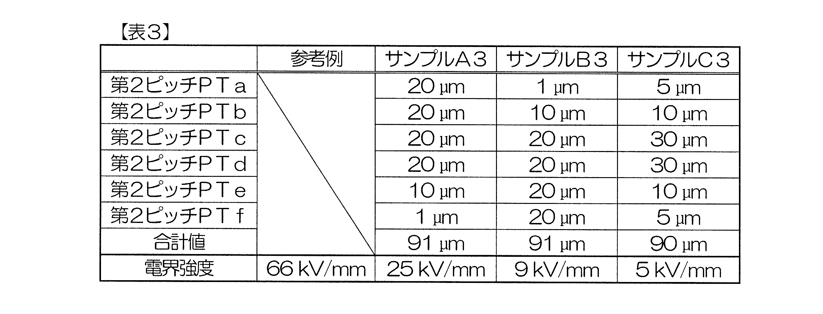
2 樹脂パッケージ
5 コントローラチップ
6 電子部品
7 ドライバチップ
13 低電圧パッド
14 高電圧パッド
20 下コイル(低電圧導体パターン)
21 上コイル(高電圧導体パターン)
27 絶縁層積層構造
28 絶縁層(第1絶縁層)
32 (上コイルの)内方領域
33 第1パッド
34 第2パッド
39 第1領域
40 第2領域
44 オーバーラップ部
45 オーバーラップ部
50 コイル間領域
75 保護膜
76 パッシベーション膜
77 樹脂膜
78 パッド開口
79 パッド開口
88 高電圧パッド層
89 低電圧パッド層
99 コイル周縁領域
101 電子部品
102 耐圧保持構造
103 第1耐圧保持構造
104 第2耐圧保持構造
108 第1ダミー導体パターン
116 第1コイル側耐圧保持構造
117 第2コイル側耐圧保持構造
118 第1パッド側耐圧保持構造
119 第2パッド側耐圧保持構造
131 電子部品
141 電子部品
142 第1螺旋パターン
143 第2螺旋パターン
151 電子部品
152 第2絶縁層 161 電子部品
162 低電圧側キャパシタ導体膜(低電圧導体パターン)
163 高電圧側キャパシタ導体膜(高電圧導体パターン)
164 第1キャパシタンス
165 第2キャパシタンス
171 電子部品
201 電子部品モジュール
Claims (39)
- 絶縁層と、
前記絶縁層内に形成された低電圧導体パターンと、
前記低電圧導体パターンと上下方向に対向するように、前記絶縁層内に形成された高電圧導体パターンと、
平面視において前記低電圧導体パターンよりも外側に張り出すように、前記絶縁層内において前記高電圧導体パターンに沿って形成された導電性の耐圧保持構造と、を含む、電子部品。 - 前記低電圧導体パターンは、螺旋状の低電圧コイルを含み、
前記高電圧導体パターンは、螺旋状の高電圧コイルを含み、
前記低電圧コイルおよび前記高電圧コイルによって変圧器が形成されている、請求項1に記載の電子部品。 - 前記耐圧保持構造は、前記高電圧コイルの螺旋パターンに対して不連続なパターンで前記高電圧コイルに沿って延びるダミー導体パターンを含む、請求項2に記載の電子部品。
- 前記ダミー導体パターンは、有端状である、請求項3に記載の電子部品。
- 前記高電圧コイルは、内側末端および外側末端を含み、
前記ダミー導体パターンは、前記高電圧コイルの前記外側末端と同電位に固定されている、請求項3または4に記載の電子部品。 - 前記高電圧コイルの前記内側末端は、平面視において前記低電圧コイルの内側の領域に位置しており、
前記高電圧コイルの前記外側末端は、平面視において前記低電圧コイルの外側の領域に位置しており、
前記ダミー導体パターンは、前記高電圧コイルの前記外側末端から引き出されている、請求項5に記載の電子部品。 - 前記耐圧保持構造は、前記高電圧コイルから離れる方向に沿って間隔を空けて形成された複数の前記ダミー導体パターンを含む、請求項3~6のいずれか一項に記載の電子部品。
- 前記高電圧コイルは、平面視で前記低電圧コイルと対向する領域において、外巻の第1螺旋領域、および、平面視で前記低電圧コイル外の領域において、前記第1螺旋領域から連続的に外巻きの第2螺旋領域を含み、
前記耐圧保持構造は、前記高電圧コイルの前記第2螺旋領域を含む、請求項2~7のいずれか一項に記載の電子部品。 - 前記高電圧コイルの第1巻回数は、前記低電圧コイルの第2巻回数よりも大きい、請求項2~7のいずれか一項に記載の電子部品。
- 前記第1巻回数および前記第2巻回数の間の差は、5以上である、請求項9に記載の電子部品。
- 前記低電圧導体パターンは、平板状の低電圧側キャパシタ導体膜を含み、
前記高電圧導体パターンは、平板状の高電圧側キャパシタ導体膜を含み、
前記低電圧側キャパシタ導体膜および前記高電圧側キャパシタ導体膜によってキャパシタンスが形成されている、請求項1に記載の電子部品。 - 前記耐圧保持構造は、前記高電圧導体パターンに沿って延び、前記高電圧導体パターンと同電位に固定されたダミー導体パターンを含む、請求項11に記載の電子部品。
- 前記ダミー導体パターンは、前記高電圧導体パターンと一体的に形成されている、請求項12に記載の電子部品。
- 前記ダミー導体パターンは、前記高電圧導体パターンから間隔を空けて形成されている、請求項12に記載の電子部品。
- 絶縁層と、
前記絶縁層内に形成された低電圧導体パターンと、
前記低電圧導体パターンと上下方向に対向するように、前記絶縁層内に形成された高電圧導体パターンと、
前記絶縁層の上に形成され、前記低電圧導体パターンに電気的に接続された低電圧パッドと、
平面視において前記低電圧パッドから間隔を空けて前記絶縁層の上に形成され、前記高電圧導体パターンに電気的に接続された高電圧パッドと、
平面視において前記高電圧パッドの周縁に沿うように、前記絶縁層内に形成された導電性のパッド側耐圧保持構造と、を含む、電子部品。 - 前記低電圧導体パターンは、螺旋状の低電圧コイルを含み、
前記高電圧導体パターンは、螺旋状の高電圧コイルを含み、
前記低電圧コイルおよび前記高電圧コイルによって変圧器が形成されている、請求項15に記載の電子部品。 - 前記パッド側耐圧保持構造は、平面視において前記高電圧コイルの螺旋パターンに対して不連続なパターンで前記高電圧パッドの周縁に沿って延びるパッド側ダミー導体パターンを含む、請求項16に記載の電子部品。
- 前記パッド側耐圧保持構造は、前記高電圧パッドから離れる方向に沿って間隔を空けて形成された複数の前記パッド側ダミー導体パターンを含む、請求項17に記載の電子部品。
- 前記高電圧パッドに最も近接する前記パッド側ダミー導体パターンおよび前記高電圧パッドの間の距離は、前記高電圧導体パターンおよび前記低電圧導体パターンの間の縦方向距離以下である、請求項18に記載の電子部品。
- 前記絶縁層内において前記高電圧導体パターンに沿って形成され、平面視において前記低電圧導体パターンよりも外側に張り出した導電性のコイル側耐圧保持構造をさらに含む、請求項18または19に記載の電子部品。
- 前記コイル側耐圧保持構造は、前記高電圧コイルの螺旋パターンに対して不連続なパターンで前記高電圧コイルに沿って引き回され、前記パッド側ダミー導体パターンと同電位に固定されたコイル側ダミー導体パターンを含む、請求項20に記載の電子部品。
- 前記コイル側ダミー導体パターンは、前記パッド側ダミー導体パターンと一体的に形成されている、請求項21に記載の電子部品。
- 前記高電圧コイルは、平面視において前記低電圧コイルの内側の領域に位置する内側末端、および、平面視において前記低電圧コイルの外側の領域に位置する外側末端を有しており、
前記高電圧パッドは、前記高電圧コイルの前記外側末端に電気的に接続されるように、前記高電圧コイルの前記外側末端の直上に配置されており、
前記パッド側耐圧保持構造は、前記絶縁層内において、前記高電圧コイルの前記外側末端に沿うように形成されている、請求項16~22のいずれか一項に記載の電子部品。 - 前記低電圧導体パターンは、平板状の低電圧側キャパシタ導体膜を含み、
前記高電圧導体パターンは、平板状の高電圧側キャパシタ導体膜を含み、
前記低電圧側キャパシタ導体膜および前記高電圧側キャパシタ導体膜によってキャパシタンスが形成されている、請求項15に記載の電子部品。 - 平面視において前記低電圧導体パターンよりも外側に張り出すように、前記絶縁層内において前記高電圧導体パターンに沿って延び、前記高電圧導体パターンと同電位に固定された導電性のキャパシタンス側耐圧保持構造を含む、請求項24に記載の電子部品。
- 前記キャパシタンス側耐圧保持構造は、前記高電圧導体パターンと一体的に形成されたキャパシタンス側ダミー導体パターンを含む、請求項25に記載の電子部品。
- 前記キャパシタンス側耐圧保持構造は、前記高電圧導体パターンから間隔を空けて形成されたキャパシタンス側ダミー導体パターンを含む、請求項25に記載の電子部品。
- 第1絶縁破壊強度を有する第1絶縁層と、
前記第1絶縁層内に形成された低電圧導体パターンと、
前記低電圧導体パターンと上下方向に対向するように、前記第1絶縁層内に形成された高電圧導体パターンと、
前記第1絶縁層内において前記第1絶縁層の表面に沿う方向に前記高電圧導体パターンから間隔を空けて形成され、前記低電圧導体パターンに電気的に接続され、前記高電圧導体パターンとの間で前記第1絶縁破壊強度以下の第1値を有する電界を形成する低電圧配線と、
前記第1絶縁層内において前記高電圧導体パターンおよび前記低電圧配線の間の領域に介在し、前記低電圧配線との間で、前記第1絶縁破壊強度以下でかつ前記第1値以上の第2値を有する電界を形成する導電性の電界増強構造と、
前記第1絶縁層の上に形成され、前記第1絶縁破壊強度以下の第2絶縁破壊強度を有する第2絶縁層と、を含む、電子部品。 - 前記電界増強構造は、前記高電圧導体パターンと同電位に固定され、かつ、前記高電圧導体パターンに沿って形成された導電性の高電圧側ダミー導体パターンを含む、請求項28に記載の電子部品。
- 前記電界増強構造は、前記低電圧配線と同電位に固定され、かつ、前記低電圧配線に沿って形成された導電性の低電圧側ダミー導体パターンを含む、請求項28または29に記載の電子部品。
- 前記第1絶縁層および前記第2絶縁層の間の領域に介在し、前記低電圧配線に電気的に接続された低電圧パッドと、
前記第1絶縁層および前記第2絶縁層の間の領域に前記低電圧パッドから間隔を空けて介在し、前記高電圧導体パターンに電気的に接続され、前記低電圧パッドとの間で前記第2絶縁破壊強度以下の電界を形成する高電圧パッドと、をさらに含む、請求項28~30のいずれか一項に記載の電子部品。 - 前記第1絶縁層の前記第1絶縁破壊強度は、5.0MV/cm以上であり、前記第2絶縁層の前記第2絶縁破壊強度は、1.0MV/cm以上である、請求項28~31のいずれか一項に記載の電子部品。
- 前記第2絶縁層は、樹脂層からなる、請求項28~32のいずれか一項に記載の電子部品。
- 前記樹脂層は、モールド樹脂を含む、請求項33に記載の電子部品。
- 前記第1絶縁層および前記第2絶縁層の間に介在するパッシベーション膜をさらに含む、請求項28~34のいずれか一項に記載の電子部品。
- 前記低電圧導体パターンは、螺旋状の低電圧コイルを含み、
前記高電圧導体パターンは、螺旋状の高電圧コイルを含み、
前記低電圧コイルおよび前記高電圧コイルによって変圧器が形成されている、請求項28~35のいずれか一項に記載の電子部品。 - 前記低電圧導体パターンは、平板状の低電圧側キャパシタ導体膜を含み、
前記高電圧導体パターンは、平板状の高電圧側キャパシタ導体膜を含み、
前記低電圧側キャパシタ導体膜および前記高電圧側キャパシタ導体膜によってキャパシタンスが形成されている、請求項28~35のいずれか一項に記載の電子部品。 - 請求項1~37のいずれか一項に記載の電子部品と、前記電子部品を封止する樹脂パッケージと、を含む、電子部品モジュール。
- 前記電子部品の前記低電圧導体パターンに電気的に接続された低電圧素子と、前記電子部品の前記高電圧導体パターンに電気的に接続された高電圧素子と、をさらに含み、前記樹脂パッケージは、前記電子部品、前記低電圧素子および前記高電圧素子を一括して封止している、請求項38に記載の電子部品モジュール。
Priority Applications (8)
| Application Number | Priority Date | Filing Date | Title |
|---|---|---|---|
| CN202310022211.4A CN115881427A (zh) | 2017-10-13 | 2018-10-15 | 电子组件 |
| CN201880066828.3A CN111213214B (zh) | 2017-10-13 | 2018-10-15 | 电子组件及电子组件模块 |
| JP2019547554A JPWO2019074130A1 (ja) | 2017-10-13 | 2018-10-15 | 電子部品および電子部品モジュール |
| DE112018004478.5T DE112018004478B4 (de) | 2017-10-13 | 2018-10-15 | Elektronikkomponente |
| US16/755,053 US11545299B2 (en) | 2017-10-13 | 2018-10-15 | Electronic component and electronic component module |
| US18/062,407 US11923128B2 (en) | 2017-10-13 | 2022-12-06 | Electronic component and electronic component module |
| US18/419,624 US12387873B2 (en) | 2017-10-13 | 2024-01-23 | Electronic component and electronic component module |
| US19/263,513 US20250336598A1 (en) | 2017-10-13 | 2025-07-09 | Electronic component and electronic component module |
Applications Claiming Priority (2)
| Application Number | Priority Date | Filing Date | Title |
|---|---|---|---|
| JP2017199877 | 2017-10-13 | ||
| JP2017-199877 | 2017-10-13 |
Related Child Applications (2)
| Application Number | Title | Priority Date | Filing Date |
|---|---|---|---|
| US16/755,053 A-371-Of-International US11545299B2 (en) | 2017-10-13 | 2018-10-15 | Electronic component and electronic component module |
| US18/062,407 Continuation US11923128B2 (en) | 2017-10-13 | 2022-12-06 | Electronic component and electronic component module |
Publications (1)
| Publication Number | Publication Date |
|---|---|
| WO2019074130A1 true WO2019074130A1 (ja) | 2019-04-18 |
Family
ID=66100722
Family Applications (1)
| Application Number | Title | Priority Date | Filing Date |
|---|---|---|---|
| PCT/JP2018/038365 Ceased WO2019074130A1 (ja) | 2017-10-13 | 2018-10-15 | 電子部品および電子部品モジュール |
Country Status (5)
| Country | Link |
|---|---|
| US (4) | US11545299B2 (ja) |
| JP (3) | JPWO2019074130A1 (ja) |
| CN (2) | CN111213214B (ja) |
| DE (1) | DE112018004478B4 (ja) |
| WO (1) | WO2019074130A1 (ja) |
Cited By (11)
| Publication number | Priority date | Publication date | Assignee | Title |
|---|---|---|---|---|
| WO2021106363A1 (ja) * | 2019-11-29 | 2021-06-03 | ローム株式会社 | 半導体装置 |
| WO2022070749A1 (ja) * | 2020-09-30 | 2022-04-07 | ローム株式会社 | 半導体装置および半導体モジュール |
| JP2022133847A (ja) * | 2021-03-02 | 2022-09-14 | 株式会社東芝 | デジタルアイソレータ |
| WO2022210549A1 (ja) * | 2021-03-29 | 2022-10-06 | ローム株式会社 | 絶縁トランス |
| WO2022210540A1 (ja) * | 2021-03-29 | 2022-10-06 | ローム株式会社 | 絶縁トランス |
| JP2023002699A (ja) * | 2020-03-19 | 2023-01-10 | 株式会社東芝 | アイソレータ |
| WO2023074137A1 (ja) * | 2021-10-25 | 2023-05-04 | ローム株式会社 | トランスチップ、信号伝達装置 |
| WO2024166718A1 (ja) * | 2023-02-09 | 2024-08-15 | ローム株式会社 | トランスチップ |
| WO2024171760A1 (ja) * | 2023-02-16 | 2024-08-22 | ローム株式会社 | 絶縁チップおよび絶縁チップの製造方法 |
| WO2024195396A1 (ja) * | 2023-03-17 | 2024-09-26 | ローム株式会社 | 絶縁チップおよび信号伝達装置 |
| WO2025009421A1 (ja) * | 2023-07-03 | 2025-01-09 | ローム株式会社 | トランスチップおよび信号伝達装置 |
Families Citing this family (1)
| Publication number | Priority date | Publication date | Assignee | Title |
|---|---|---|---|---|
| CN114675444A (zh) * | 2020-12-10 | 2022-06-28 | 群创光电股份有限公司 | 电子装置 |
Citations (3)
| Publication number | Priority date | Publication date | Assignee | Title |
|---|---|---|---|---|
| JP2016028407A (ja) * | 2013-11-13 | 2016-02-25 | ローム株式会社 | 半導体装置および半導体モジュール |
| WO2016080034A1 (ja) * | 2014-11-18 | 2016-05-26 | 三菱電機株式会社 | 信号伝送絶縁デバイス及びパワー半導体モジュール |
| JP2017073475A (ja) * | 2015-10-08 | 2017-04-13 | パナソニックIpマネジメント株式会社 | 積層コイル部品 |
Family Cites Families (26)
| Publication number | Priority date | Publication date | Assignee | Title |
|---|---|---|---|---|
| JPS54110424A (en) * | 1978-02-17 | 1979-08-29 | Ricoh Co Ltd | Transformer |
| USPP17326P3 (en) * | 2004-07-27 | 2007-01-02 | Syngenta Seeds B.V. | Bidens ferulifolia plant named ‘Bidcomtis’ |
| TWI330863B (en) * | 2005-05-18 | 2010-09-21 | Megica Corp | Semiconductor chip with coil element over passivation layer |
| JP5324829B2 (ja) * | 2008-06-05 | 2013-10-23 | ルネサスエレクトロニクス株式会社 | 半導体装置 |
| US8278730B2 (en) | 2009-10-28 | 2012-10-02 | Infineon Technologies Austria Ag | High voltage resistance coupling structure |
| JP2012129217A (ja) * | 2010-11-24 | 2012-07-05 | Daido Steel Co Ltd | 圧粉磁心のための加圧成形用粉体及び圧粉磁心の製造方法 |
| US8716832B2 (en) | 2011-09-27 | 2014-05-06 | Infineon Technologies Ag | Semiconductor structure including guard ring |
| US9048019B2 (en) * | 2011-09-27 | 2015-06-02 | Infineon Technologies Ag | Semiconductor structure including guard ring |
| JP5800691B2 (ja) | 2011-11-25 | 2015-10-28 | ルネサスエレクトロニクス株式会社 | トランス |
| US8665054B2 (en) * | 2012-04-20 | 2014-03-04 | Infineon Technologies Austria Ag | Semiconductor component with coreless transformer |
| JP5964183B2 (ja) | 2012-09-05 | 2016-08-03 | ルネサスエレクトロニクス株式会社 | 半導体装置 |
| JP5741615B2 (ja) * | 2013-03-14 | 2015-07-01 | Tdk株式会社 | 電子部品及びその製造方法 |
| US9653396B2 (en) * | 2013-03-25 | 2017-05-16 | Renesas Electronics Corporation | Semiconductor device and method of manufacturing the same |
| JP6129659B2 (ja) | 2013-06-25 | 2017-05-17 | ルネサスエレクトロニクス株式会社 | 半導体装置およびその製造方法 |
| US9711451B2 (en) | 2014-01-29 | 2017-07-18 | Renesas Electronics Corporation | Semiconductor device with coils in different wiring layers |
| JP6344137B2 (ja) * | 2014-08-19 | 2018-06-20 | 富士電機株式会社 | 半導体装置及びその製造方法 |
| JP5968968B2 (ja) * | 2014-09-19 | 2016-08-10 | ルネサスエレクトロニクス株式会社 | 半導体装置 |
| JP5889501B1 (ja) | 2014-11-18 | 2016-03-22 | 三菱電機株式会社 | 信号伝送絶縁デバイス及びパワー半導体モジュール |
| DE112015006450T5 (de) * | 2015-04-14 | 2017-12-28 | Mitsubishi Electric Corporation | Halbleitereinheit |
| US10204732B2 (en) * | 2015-10-23 | 2019-02-12 | Analog Devices Global | Dielectric stack, an isolator device and method of forming an isolator device |
| JP2017199877A (ja) | 2016-04-28 | 2017-11-02 | キヤノン株式会社 | 光増幅器、それを備える光干渉断層計、及び光増幅器を用いた光増幅方法 |
| JP6841634B2 (ja) | 2016-11-08 | 2021-03-10 | ローム株式会社 | 電子部品 |
| JP7301950B2 (ja) * | 2019-02-28 | 2023-07-03 | 富士フイルム株式会社 | 給電部材、コイル配置用磁性シート、及びコイル配置用磁性シートの製造方法 |
| DE112019002216T5 (de) * | 2019-03-08 | 2021-02-18 | Rohm Co., Ltd. | Elektronikkomponente |
| CN113410018B (zh) * | 2021-06-25 | 2022-11-18 | 深圳市铂科新材料股份有限公司 | 一种磁性复合材料三维结构、其加工方法和用途 |
| JP2023135812A (ja) * | 2022-03-16 | 2023-09-29 | セイコーエプソン株式会社 | 絶縁物被覆軟磁性粉末の製造方法、絶縁物被覆軟磁性粉末、圧粉磁心、磁性素子、電子機器および移動体 |
-
2018
- 2018-10-15 DE DE112018004478.5T patent/DE112018004478B4/de active Active
- 2018-10-15 JP JP2019547554A patent/JPWO2019074130A1/ja active Pending
- 2018-10-15 US US16/755,053 patent/US11545299B2/en active Active
- 2018-10-15 CN CN201880066828.3A patent/CN111213214B/zh active Active
- 2018-10-15 WO PCT/JP2018/038365 patent/WO2019074130A1/ja not_active Ceased
- 2018-10-15 CN CN202310022211.4A patent/CN115881427A/zh active Pending
-
2021
- 2021-05-25 JP JP2021087737A patent/JP7220743B2/ja active Active
-
2022
- 2022-12-06 US US18/062,407 patent/US11923128B2/en active Active
-
2023
- 2023-01-31 JP JP2023013538A patent/JP7564263B2/ja active Active
-
2024
- 2024-01-23 US US18/419,624 patent/US12387873B2/en active Active
-
2025
- 2025-07-09 US US19/263,513 patent/US20250336598A1/en active Pending
Patent Citations (3)
| Publication number | Priority date | Publication date | Assignee | Title |
|---|---|---|---|---|
| JP2016028407A (ja) * | 2013-11-13 | 2016-02-25 | ローム株式会社 | 半導体装置および半導体モジュール |
| WO2016080034A1 (ja) * | 2014-11-18 | 2016-05-26 | 三菱電機株式会社 | 信号伝送絶縁デバイス及びパワー半導体モジュール |
| JP2017073475A (ja) * | 2015-10-08 | 2017-04-13 | パナソニックIpマネジメント株式会社 | 積層コイル部品 |
Cited By (21)
| Publication number | Priority date | Publication date | Assignee | Title |
|---|---|---|---|---|
| WO2021106363A1 (ja) * | 2019-11-29 | 2021-06-03 | ローム株式会社 | 半導体装置 |
| JPWO2021106363A1 (ja) * | 2019-11-29 | 2021-06-03 | ||
| JP7674261B2 (ja) | 2019-11-29 | 2025-05-09 | ローム株式会社 | 半導体装置 |
| US12199136B2 (en) | 2019-11-29 | 2025-01-14 | Rohm Co., Ltd. | Semiconductor device |
| JP7332775B2 (ja) | 2020-03-19 | 2023-08-23 | 株式会社東芝 | アイソレータ |
| JP2023002699A (ja) * | 2020-03-19 | 2023-01-10 | 株式会社東芝 | アイソレータ |
| WO2022070749A1 (ja) * | 2020-09-30 | 2022-04-07 | ローム株式会社 | 半導体装置および半導体モジュール |
| JPWO2022070749A1 (ja) * | 2020-09-30 | 2022-04-07 | ||
| JP7784383B2 (ja) | 2020-09-30 | 2025-12-11 | ローム株式会社 | 半導体装置および半導体モジュール |
| JP2022133847A (ja) * | 2021-03-02 | 2022-09-14 | 株式会社東芝 | デジタルアイソレータ |
| JPWO2022210540A1 (ja) * | 2021-03-29 | 2022-10-06 | ||
| JPWO2022210549A1 (ja) * | 2021-03-29 | 2022-10-06 | ||
| JP7803936B2 (ja) | 2021-03-29 | 2026-01-21 | ローム株式会社 | 絶縁トランス |
| JP7803935B2 (ja) | 2021-03-29 | 2026-01-21 | ローム株式会社 | 絶縁トランス |
| WO2022210540A1 (ja) * | 2021-03-29 | 2022-10-06 | ローム株式会社 | 絶縁トランス |
| WO2022210549A1 (ja) * | 2021-03-29 | 2022-10-06 | ローム株式会社 | 絶縁トランス |
| WO2023074137A1 (ja) * | 2021-10-25 | 2023-05-04 | ローム株式会社 | トランスチップ、信号伝達装置 |
| WO2024166718A1 (ja) * | 2023-02-09 | 2024-08-15 | ローム株式会社 | トランスチップ |
| WO2024171760A1 (ja) * | 2023-02-16 | 2024-08-22 | ローム株式会社 | 絶縁チップおよび絶縁チップの製造方法 |
| WO2024195396A1 (ja) * | 2023-03-17 | 2024-09-26 | ローム株式会社 | 絶縁チップおよび信号伝達装置 |
| WO2025009421A1 (ja) * | 2023-07-03 | 2025-01-09 | ローム株式会社 | トランスチップおよび信号伝達装置 |
Also Published As
| Publication number | Publication date |
|---|---|
| CN111213214A (zh) | 2020-05-29 |
| JP7220743B2 (ja) | 2023-02-10 |
| CN111213214B (zh) | 2023-07-21 |
| US11923128B2 (en) | 2024-03-05 |
| JP2023055832A (ja) | 2023-04-18 |
| US11545299B2 (en) | 2023-01-03 |
| US20230107689A1 (en) | 2023-04-06 |
| JP2021132232A (ja) | 2021-09-09 |
| US20240161972A1 (en) | 2024-05-16 |
| CN115881427A (zh) | 2023-03-31 |
| US12387873B2 (en) | 2025-08-12 |
| US20210193380A1 (en) | 2021-06-24 |
| US20250336598A1 (en) | 2025-10-30 |
| DE112018004478T5 (de) | 2020-07-30 |
| DE112018004478B4 (de) | 2025-03-27 |
| JP7564263B2 (ja) | 2024-10-08 |
| JPWO2019074130A1 (ja) | 2020-11-26 |
Similar Documents
| Publication | Publication Date | Title |
|---|---|---|
| JP7220743B2 (ja) | 絶縁型部品およびモジュール | |
| US20230298805A1 (en) | Semiconductor device and semiconductor module | |
| JP7429672B2 (ja) | 絶縁通信部品およびモジュール | |
| JP6591637B2 (ja) | 半導体装置および半導体モジュール | |
| JP7824273B2 (ja) | 絶縁モジュールおよびゲートドライバ | |
| CN114762114A (zh) | 半导体装置 | |
| WO2022070749A1 (ja) | 半導体装置および半導体モジュール | |
| US20250300119A1 (en) | Semiconductor device, method for designing the same, and method for manufacturing the same |
Legal Events
| Date | Code | Title | Description |
|---|---|---|---|
| 121 | Ep: the epo has been informed by wipo that ep was designated in this application |
Ref document number: 18866809 Country of ref document: EP Kind code of ref document: A1 |
|
| ENP | Entry into the national phase |
Ref document number: 2019547554 Country of ref document: JP Kind code of ref document: A |
|
| 122 | Ep: pct application non-entry in european phase |
Ref document number: 18866809 Country of ref document: EP Kind code of ref document: A1 |
|
| WWG | Wipo information: grant in national office |
Ref document number: 112018004478 Country of ref document: DE |