WO2019062245A1 - 移位寄存器、其驱动方法、栅极驱动电路及显示装置 - Google Patents
移位寄存器、其驱动方法、栅极驱动电路及显示装置 Download PDFInfo
- Publication number
- WO2019062245A1 WO2019062245A1 PCT/CN2018/093854 CN2018093854W WO2019062245A1 WO 2019062245 A1 WO2019062245 A1 WO 2019062245A1 CN 2018093854 W CN2018093854 W CN 2018093854W WO 2019062245 A1 WO2019062245 A1 WO 2019062245A1
- Authority
- WO
- WIPO (PCT)
- Prior art keywords
- switching transistor
- signal
- node
- pole
- control
- Prior art date
- Legal status (The legal status is an assumption and is not a legal conclusion. Google has not performed a legal analysis and makes no representation as to the accuracy of the status listed.)
- Ceased
Links
Images
Classifications
-
- G—PHYSICS
- G09—EDUCATION; CRYPTOGRAPHY; DISPLAY; ADVERTISING; SEALS
- G09G—ARRANGEMENTS OR CIRCUITS FOR CONTROL OF INDICATING DEVICES USING STATIC MEANS TO PRESENT VARIABLE INFORMATION
- G09G3/00—Control arrangements or circuits, of interest only in connection with visual indicators other than cathode-ray tubes
- G09G3/20—Control arrangements or circuits, of interest only in connection with visual indicators other than cathode-ray tubes for presentation of an assembly of a number of characters, e.g. a page, by composing the assembly by combination of individual elements arranged in a matrix no fixed position being assigned to or needed to be assigned to the individual characters or partial characters
-
- G—PHYSICS
- G09—EDUCATION; CRYPTOGRAPHY; DISPLAY; ADVERTISING; SEALS
- G09G—ARRANGEMENTS OR CIRCUITS FOR CONTROL OF INDICATING DEVICES USING STATIC MEANS TO PRESENT VARIABLE INFORMATION
- G09G3/00—Control arrangements or circuits, of interest only in connection with visual indicators other than cathode-ray tubes
- G09G3/20—Control arrangements or circuits, of interest only in connection with visual indicators other than cathode-ray tubes for presentation of an assembly of a number of characters, e.g. a page, by composing the assembly by combination of individual elements arranged in a matrix no fixed position being assigned to or needed to be assigned to the individual characters or partial characters
- G09G3/22—Control arrangements or circuits, of interest only in connection with visual indicators other than cathode-ray tubes for presentation of an assembly of a number of characters, e.g. a page, by composing the assembly by combination of individual elements arranged in a matrix no fixed position being assigned to or needed to be assigned to the individual characters or partial characters using controlled light sources
- G09G3/30—Control arrangements or circuits, of interest only in connection with visual indicators other than cathode-ray tubes for presentation of an assembly of a number of characters, e.g. a page, by composing the assembly by combination of individual elements arranged in a matrix no fixed position being assigned to or needed to be assigned to the individual characters or partial characters using controlled light sources using electroluminescent panels
- G09G3/32—Control arrangements or circuits, of interest only in connection with visual indicators other than cathode-ray tubes for presentation of an assembly of a number of characters, e.g. a page, by composing the assembly by combination of individual elements arranged in a matrix no fixed position being assigned to or needed to be assigned to the individual characters or partial characters using controlled light sources using electroluminescent panels semiconductive, e.g. using light-emitting diodes [LED]
- G09G3/3208—Control arrangements or circuits, of interest only in connection with visual indicators other than cathode-ray tubes for presentation of an assembly of a number of characters, e.g. a page, by composing the assembly by combination of individual elements arranged in a matrix no fixed position being assigned to or needed to be assigned to the individual characters or partial characters using controlled light sources using electroluminescent panels semiconductive, e.g. using light-emitting diodes [LED] organic, e.g. using organic light-emitting diodes [OLED]
- G09G3/3266—Details of drivers for scan electrodes
-
- G—PHYSICS
- G09—EDUCATION; CRYPTOGRAPHY; DISPLAY; ADVERTISING; SEALS
- G09G—ARRANGEMENTS OR CIRCUITS FOR CONTROL OF INDICATING DEVICES USING STATIC MEANS TO PRESENT VARIABLE INFORMATION
- G09G3/00—Control arrangements or circuits, of interest only in connection with visual indicators other than cathode-ray tubes
- G09G3/20—Control arrangements or circuits, of interest only in connection with visual indicators other than cathode-ray tubes for presentation of an assembly of a number of characters, e.g. a page, by composing the assembly by combination of individual elements arranged in a matrix no fixed position being assigned to or needed to be assigned to the individual characters or partial characters
- G09G3/34—Control arrangements or circuits, of interest only in connection with visual indicators other than cathode-ray tubes for presentation of an assembly of a number of characters, e.g. a page, by composing the assembly by combination of individual elements arranged in a matrix no fixed position being assigned to or needed to be assigned to the individual characters or partial characters by control of light from an independent source
- G09G3/36—Control arrangements or circuits, of interest only in connection with visual indicators other than cathode-ray tubes for presentation of an assembly of a number of characters, e.g. a page, by composing the assembly by combination of individual elements arranged in a matrix no fixed position being assigned to or needed to be assigned to the individual characters or partial characters by control of light from an independent source using liquid crystals
- G09G3/3611—Control of matrices with row and column drivers
- G09G3/3674—Details of drivers for scan electrodes
- G09G3/3677—Details of drivers for scan electrodes suitable for active matrices only
-
- G—PHYSICS
- G11—INFORMATION STORAGE
- G11C—STATIC STORES
- G11C19/00—Digital stores in which the information is moved stepwise, e.g. shift registers
- G11C19/28—Digital stores in which the information is moved stepwise, e.g. shift registers using semiconductor elements
-
- G—PHYSICS
- G09—EDUCATION; CRYPTOGRAPHY; DISPLAY; ADVERTISING; SEALS
- G09G—ARRANGEMENTS OR CIRCUITS FOR CONTROL OF INDICATING DEVICES USING STATIC MEANS TO PRESENT VARIABLE INFORMATION
- G09G2310/00—Command of the display device
- G09G2310/02—Addressing, scanning or driving the display screen or processing steps related thereto
- G09G2310/0264—Details of driving circuits
- G09G2310/0267—Details of drivers for scan electrodes, other than drivers for liquid crystal, plasma or OLED displays
-
- G—PHYSICS
- G09—EDUCATION; CRYPTOGRAPHY; DISPLAY; ADVERTISING; SEALS
- G09G—ARRANGEMENTS OR CIRCUITS FOR CONTROL OF INDICATING DEVICES USING STATIC MEANS TO PRESENT VARIABLE INFORMATION
- G09G2310/00—Command of the display device
- G09G2310/02—Addressing, scanning or driving the display screen or processing steps related thereto
- G09G2310/0264—Details of driving circuits
- G09G2310/0286—Details of a shift registers arranged for use in a driving circuit
-
- G—PHYSICS
- G09—EDUCATION; CRYPTOGRAPHY; DISPLAY; ADVERTISING; SEALS
- G09G—ARRANGEMENTS OR CIRCUITS FOR CONTROL OF INDICATING DEVICES USING STATIC MEANS TO PRESENT VARIABLE INFORMATION
- G09G2310/00—Command of the display device
- G09G2310/08—Details of timing specific for flat panels, other than clock recovery
-
- G—PHYSICS
- G09—EDUCATION; CRYPTOGRAPHY; DISPLAY; ADVERTISING; SEALS
- G09G—ARRANGEMENTS OR CIRCUITS FOR CONTROL OF INDICATING DEVICES USING STATIC MEANS TO PRESENT VARIABLE INFORMATION
- G09G2320/00—Control of display operating conditions
- G09G2320/04—Maintaining the quality of display appearance
- G09G2320/043—Preventing or counteracting the effects of ageing
Definitions
- the present disclosure relates to the field of display technologies, and in particular, to a shift register, a driving method thereof, a gate driving circuit, and a display device.
- the general gate driving circuit is composed of a plurality of cascaded shift registers, and the driving signal output ends of the shift registers of the respective stages are respectively connected with a gate line, and sequentially realize the rows on the display panel through the shift registers of each stage.
- the gate line inputs the scan signal.
- the output transistor generally supplies a high voltage signal to the drive signal output terminal to output a valid scan signal under the control of the pull-up node, and the high voltage signal flows through the same output while the display panel is displayed.
- the transistor and the gate of the output transistor are in the same bias for a long time, resulting in characteristic drift of the output transistor and reduced lifetime. As a result, the stability and the service life of the shift register are degraded, which is disadvantageous for the long-term stable use of the display panel.
- An embodiment of the present disclosure provides a shift register, including:
- An input circuit configured to provide the signal of the input signal end to the first node under the control of the input signal end;
- the reset circuit is configured to provide a signal of the reference voltage signal end to the first node under the control of the reset signal end;
- the first control circuit is configured to control a potential of the first node and a potential of the second node;
- a first output circuit configured to provide a signal of the first clock signal end to a driving signal of the shift register under common control of a signal of the first clock signal end and a signal of the first node And outputting, by the second clock signal end and the signal of the first node, a signal of the second clock signal end to the driving signal output end; wherein, the signal of the first clock signal end is The signals of the second clock signal end have the same period and opposite phases;
- a second output circuit configured to supply the signal of the reference voltage signal end to the driving signal output end under the control of the input signal end and the signal of the second node, respectively.
- the first output circuit includes: a first switching transistor, a second switching transistor, a third switching transistor, a fourth switching transistor, and a storage capacitor;
- a control electrode of the first switching transistor is connected to the first node, a first pole of the first switching transistor is connected to the first clock signal end, and a second pole of the first switching transistor is a control pole of the second switching transistor is connected;
- a first pole of the second switching transistor is connected to the first clock signal end, and a second pole of the second switching transistor is connected to the driving signal output end;
- a control electrode of the third switching transistor is connected to the first node, a first pole of the third switching transistor is connected to the second clock signal end, and a second pole of the third switching transistor is a control pole of the fourth switching transistor is connected;
- a first pole of the fourth switching transistor is connected to the second clock signal end, and a second pole of the fourth switching transistor is connected to the driving signal output end;
- the storage capacitor is connected between the first node and the output of the driving signal.
- the input circuit includes: a fifth switching transistor; wherein a control pole of the fifth switching transistor and a first pole thereof are connected to the input signal end The second pole of the fifth switching transistor is connected to the first node.
- the reset circuit includes: a sixth switching transistor; wherein a control electrode of the sixth switching transistor is connected to the reset signal end, the sixth A first pole of the switching transistor is coupled to the reference voltage signal terminal, and a second pole of the sixth switching transistor is coupled to the first node.
- the second output circuit includes: a seventh switching transistor and an eighth switching transistor;
- a control electrode of the seventh switching transistor is connected to the second node, a first pole of the seventh switching transistor is connected to the reference voltage signal end, and a second pole of the seventh switching transistor is connected to the driving The signal outputs are connected;
- a control electrode of the eighth switching transistor is connected to the input signal terminal, a first pole of the eighth switching transistor is connected to the reference voltage signal terminal, and a second pole of the eighth switching transistor is coupled to the driving The signal outputs are connected.
- the first control circuit includes: a ninth switch transistor, a tenth switch transistor, an eleventh switch transistor, a twelfth switch transistor, and a thirteenth switch Transistor
- a control pole of the ninth switching transistor is connected to the second node, a first pole of the ninth switching transistor is connected to the reference voltage signal end, and a second pole of the ninth switching transistor is opposite to the first Connected to a node;
- the control electrode of the tenth switching transistor is connected to the first node control signal end, and the second electrode of the tenth switching transistor is connected to the control electrode of the eleventh switching transistor;
- a first pole of the eleventh switching transistor is connected to the first node control signal end, and a second pole of the eleventh switching transistor is connected to the second node;
- a control electrode of the twelfth switching transistor is connected to the first node, a first pole of the twelfth switching transistor is connected to the reference voltage signal end, and a second pole of the twelfth switching transistor is The control poles of the eleventh switching transistor are connected;
- a control electrode of the thirteenth switching transistor is connected to the first node, a first pole of the thirteenth switching transistor is connected to the reference voltage signal end, and a second pole of the thirteenth switching transistor is The second node is connected.
- a period of a signal of the first clock signal end is 4 s, and a signal duty ratio of the first clock signal end is 50%.
- the shift register further includes: a second control circuit and a third output circuit;
- the second control circuit is configured to control a potential of the first node and a potential of a third node
- the third output circuit is configured to provide a signal of the reference voltage signal end to the driving signal output end under the control of a signal of the third node.
- the second control circuit includes: a fourteenth switching transistor, a fifteenth switching transistor, a sixteenth switching transistor, a seventeenth switching transistor, and a tenth Eight-switch transistor
- a control electrode of the fourteenth switching transistor is connected to the third node, a first pole of the fourteenth switching transistor is connected to the reference voltage signal end, and a second pole of the fourteenth switching transistor is The first node is connected;
- control pole of the fifteenth switching transistor and the first pole thereof are both connected to the second node control signal end, and the second pole of the fifteenth switching transistor is connected to the control pole of the sixteenth switching transistor;
- a first pole of the sixteenth switching transistor is connected to the second node control signal end, and a second pole of the sixteenth switching transistor is connected to the third node;
- a control electrode of the seventeenth switching transistor is connected to the first node, a first pole of the seventeenth switching transistor is connected to the reference voltage signal end, and a second pole of the seventeenth switching transistor is The control poles of the sixteenth switching transistor are connected;
- a control electrode of the eighteenth switching transistor is connected to the first node, a first pole of the eighteenth switching transistor is connected to the reference voltage signal end, and a second pole of the eighteenth switching transistor is The third node is connected.
- the signal of the first node control signal end and the signal of the second node control signal end are respectively clock signals; and the signal of the first node control signal end is The signals of the second node control signal end have the same period and opposite phases.
- the third output circuit includes: a nineteenth switch transistor
- a control electrode of the nineteenth switching transistor is connected to the third node, a first pole of the nineteenth switching transistor is connected to the reference voltage signal end, and a second pole of the nineteenth switching transistor is The drive signal outputs are connected.
- the shift register further includes: an output stabilization circuit; the output stabilization circuit is configured to: at the end of the reset signal end, the reference voltage signal end A signal is provided to the drive signal output.
- the output stabilization circuit includes: a twentieth switching transistor
- a control electrode of the twentieth switching transistor is connected to the reset signal terminal, a first pole of the twentieth switching transistor is connected to the reference voltage signal terminal, and a second pole of the twentieth switching transistor is The drive signal outputs are connected.
- an embodiment of the present disclosure further provides a driving method for the above shift register, including:
- a signal having the same period and opposite phase is input to the first clock signal terminal and the second clock signal terminal.
- an embodiment of the present disclosure further provides a gate driving circuit, including any one of the above-mentioned shift registers provided by the plurality of embodiments of the present disclosure;
- the input signal end of the first stage shift register is connected to the first frame trigger signal end;
- the input signal end of the second stage shift register is connected to the second frame trigger signal end;
- the input signal end of the third stage shift register is connected to the third frame trigger signal end;
- the input signal terminal of the fourth shift register is connected to the drive signal output end of the first shift register
- the reset signal terminal of the first shift register is connected to the drive signal output terminal of the fifth shift register.
- the first clock signal end of each shift register of each stage is connected to the first clock end, and the second stage of each shift register is The clock signal ends are all connected to the second clock terminal.
- an embodiment of the present disclosure further provides a display device including any of the above-described gate driving circuits provided by the embodiments of the present disclosure.
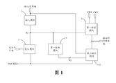
- FIG. 1 is a schematic structural diagram of a shift register according to some embodiments of the present disclosure
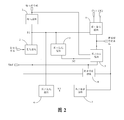
- FIG. 2 is a schematic structural diagram of a shift register according to some embodiments of the present disclosure.
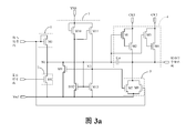
- 3a is a schematic structural diagram of a shift register provided by some embodiments of the present disclosure.
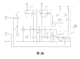
- FIG. 3b is a schematic structural diagram of a shift register according to some embodiments of the present disclosure.
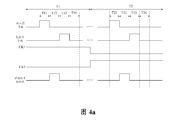
- 4a is a timing diagram of input and output corresponding to the shift register shown in FIG. 3a;
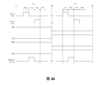
- 4b is a timing diagram of input and output corresponding to the shift register shown in FIG. 3b;
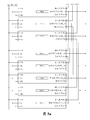
- 5a is a schematic structural diagram of a gate driving circuit according to some embodiments of the present disclosure.
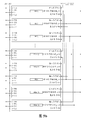
- FIG. 5b is a schematic structural diagram of a gate driving circuit according to some embodiments of the present disclosure.
- a shift register provided by an embodiment of the present disclosure includes: an input circuit 1, a reset circuit 2, a first control circuit 3, a first output circuit 4, and a second output circuit 5;
- the input circuit 1 is used to supply the signal of the input signal terminal Input to the first node N1 under the control of the input signal terminal Input;
- the reset circuit 2 is configured to provide a signal of the reference voltage signal terminal Vref to the first node N1 under the control of the reset signal terminal Reset;
- the first control circuit 3 is configured to control the potential of the first node N1 and the potential of the second node N2;
- the first output circuit 4 is configured to supply the signal of the first clock signal terminal CK1 to the driving signal output terminal Output of the shift register under the common control of the signals of the first clock signal terminal CK1 and the first node N1, at the second clock
- the signal of the second clock signal terminal CK2 is supplied to the driving signal output terminal Output under the joint control of the signal of the signal terminal CK2 and the signal of the first node N1; wherein the signal of the first clock signal terminal CK1 and the signal of the second clock signal terminal CK2
- the cycles are the same and the phases are opposite;
- the second output circuit 5 is configured to supply the signal of the reference voltage signal terminal Vref to the driving signal output terminal Output under the control of the signal of the input signal terminal Input and the second node N2, respectively.
- the shift register provided by the embodiment of the present disclosure has two output channels, one of which is a first clock signal end under the common control of the signals of the first clock signal terminal CK1 and the first node N1.
- the signal of CK1 is supplied to the driving signal output terminal Output of the shift register, and the other path is to supply the signal of the second clock signal terminal CK2 to the driving signal under the common control of the signals of the second clock signal terminal CK2 and the first node N1.
- the output is output, and interacts with the other four circuits, so that the two paths can work alternately, so that current can only be prevented from flowing through only one path, thereby improving the service life of the shift register.
- the period of the signal of the first clock signal terminal CK1 may be M seconds, where M is a positive number.
- the period of the signal of the first clock signal terminal CK1 may also be the time at which N frames are displayed, where N is a positive integer.
- the period of the signal of the first clock signal terminal CK1 may also be the time of scanning the K line pixels, where K is a positive integer.
- the period of the signal of the first clock signal terminal CK1 may be 4 s, and the signal duty ratio of the first clock signal terminal CK1 may be 50%.
- 4s may include a time for displaying 240 frames.
- the period of the signal of the first clock signal terminal CK1 needs to be determined according to the actual application environment, which is not limited herein.
- the input circuit 1 is respectively connected to the input signal terminal Input and the first node N1; the reset circuit 2 and the reset signal end are respectively The reference voltage signal terminal Vref is connected to the first node N1; the first control circuit 3 is connected to the first node N1 and the second node N2, respectively; the first output circuit 4 is respectively coupled to the first clock signal terminal CK1, the first node N1, and the first node The driving signal output terminal Output of the bit register and the second clock signal terminal CK2 are connected; the second output circuit 5 is respectively connected to the input signal terminal Input, the second node N2, the reference voltage signal terminal Vref and the driving signal output terminal Output.
- the effective pulse signal of the input signal terminal Input is a high potential signal
- the signal of the reference voltage signal terminal Vref may be a low potential signal
- the effective pulse signal of the input signal terminal Input is a low potential signal
- the signal of the reference voltage signal terminal Vref may be a high potential signal.
- the input circuit 1 may include: a fifth switching transistor M5;
- the control electrode of the fifth switching transistor M5 and its first pole are both connected to the input signal terminal Input, and the second pole of the fifth switching transistor M5 is connected to the first node N1.
- the fifth switching transistor M5 may be an N-type transistor; or the fifth switching transistor M5 may be a P-type transistor, which is not limited herein.
- the reset circuit 2 may include: a sixth switching transistor M6;
- the control electrode of the sixth switching transistor M6 is connected to the reset signal terminal Reset, the first pole of the sixth switching transistor M6 is connected to the reference voltage signal terminal Vref, and the second pole of the sixth switching transistor M6 is connected to the first node N1.
- the sixth switching transistor M6 may be an N-type transistor.
- the sixth switching transistor M6 may be a P-type transistor, which is not limited herein.
- the first control circuit 3 is configured to control the potentials of the first node N1 and the second node N2, taking the effective pulse signal of the input signal terminal Input as a high-potential signal as an example, and the first control circuit 3 can realize the display
- the potential of the first node N1 is at a high potential from the start of the input to the end of the output in the frame time, and the potential of the second node N2 is at a low potential, and the potential of the first node N1 is low when the input is completed from the end of the output to the next frame.
- the function of the potential of the second node N2 is a high potential, which is within the scope of the protection of the present disclosure, and is not limited herein.
- the first control circuit 3 may include: a ninth switching transistor M9, a tenth switching transistor M10, and an eleventh switching transistor. M11, the twelfth switching transistor M12 and the thirteenth switching transistor M13;
- the control electrode of the ninth switching transistor M9 is connected to the second node N2, the first pole of the ninth switching transistor M9 is connected to the reference voltage signal terminal Vref, and the second pole of the ninth switching transistor M9 is connected to the first node N1;
- the control pole of the tenth switching transistor M10 and its first pole are both connected to the first node control signal terminal VN1, and the second pole of the tenth switching transistor M10 is connected to the control electrode of the eleventh switching transistor M11;
- the first pole of the eleventh switching transistor M11 is connected to the first node control signal terminal VN1, and the second pole of the eleventh switching transistor M11 is connected to the second node N2;
- the control electrode of the twelfth switching transistor M12 is connected to the first node N1, the first pole of the twelfth switching transistor M12 is connected to the reference voltage signal terminal Vref, and the second pole and the eleventh switching transistor of the twelfth switching transistor M12 are connected.
- the control poles of the M11 are connected;
- the control electrode of the thirteenth switching transistor M13 is connected to the first node N1, the first pole of the thirteenth switching transistor M13 is connected to the reference voltage signal terminal Vref, and the second pole of the thirteenth switching transistor M13 is connected to the second node N2. .
- the signal of the first node control signal terminal VN1 when the effective pulse signal of the input signal terminal Input is a high potential signal, the signal of the first node control signal terminal VN1 may be a high potential signal. When the effective pulse signal of the input signal terminal Input is a low potential signal, the signal of the first node control signal terminal VN1 may be a low potential signal.
- the signal of the first node control signal terminal VN1 may also be a clock signal, which is not limited herein.
- the size of the twelfth switching transistor M12 is generally set larger than the size of the tenth switching transistor M10 during the process preparation, so that when the potential of the first node N1 is high, the twelfth switching transistor M12 provides a signal of the reference voltage signal terminal Vref to the control electrode of the eleventh switching transistor M11 at a rate greater than that of the tenth switching transistor M10 under the control of the signal of the first node N1, under the control of the first node control signal terminal VN1
- the signal of the first node control signal terminal VN1 is supplied to the gate of the eleventh switching transistor M11, thereby ensuring that the potential of the second node N2 is low.
- the ninth switching transistor M9, the tenth switching transistor M10, the eleventh switching transistor M11, the twelfth switching transistor M12, and the thirteenth switching transistor M13 may be N-type. Transistor.
- the ninth switching transistor M9, the tenth switching transistor M10, the eleventh switching transistor M11, the twelfth switching transistor M12, and the thirteenth switching transistor M13 may be P-type transistors, which are not limited herein.
- the first output circuit 4 may include: a first switching transistor M1, a second switching transistor M2, and a third switching transistor M3. a fourth switching transistor M4 and a storage capacitor Cst;
- the control electrode of the first switching transistor M1 is connected to the first node N1, the first pole of the first switching transistor M1 is connected to the first clock signal terminal CK1, and the second pole of the first switching transistor M1 is controlled by the second switching transistor M2. Extremely connected
- the first pole of the second switching transistor M2 is connected to the first clock signal terminal CK1, and the second pole of the second switching transistor M2 is connected to the driving signal output terminal Output;
- the control pole of the third switching transistor M3 is connected to the first node N1, the first pole of the third switching transistor M3 is connected to the second clock signal terminal CK2, and the second pole of the third switching transistor M3 is controlled by the fourth switching transistor M4. Extremely connected
- the first pole of the fourth switching transistor M4 is connected to the second clock signal terminal CK2, and the second pole of the fourth switching transistor M4 is connected to the driving signal output terminal Output;
- the storage capacitor Cst is connected between the first node N1 and the driving signal output terminal Output; wherein the storage capacitor Cst can be charged or discharged under the control of the signal of the first node N1 and the driving signal output terminal Output, and due to the storage capacitor Cst For this reason, the voltage difference between the first node N1 and the drive signal output terminal can be kept stable.
- the first switching transistor M1, the second switching transistor M2, the third switching transistor M3, and the fourth switching transistor M4 may be N-type transistors; or, the first switching transistor M1
- the second switching transistor M2, the third switching transistor M3, and the fourth switching transistor M4 may be P-type transistors, which are not limited herein.
- the second output circuit 5 may include: a seventh switching transistor M7 and an eighth switching transistor M8;
- the control electrode of the seventh switching transistor M7 is connected to the second node N2, the first pole of the seventh switching transistor M7 is connected to the reference voltage signal terminal Vref, and the second pole of the seventh switching transistor M7 is connected to the driving signal output terminal Output;
- the control electrode of the eighth switching transistor M8 is connected to the input signal terminal Input, the first pole of the eighth switching transistor M8 is connected to the reference voltage signal terminal Vref, and the second pole of the eighth switching transistor M8 is connected to the driving signal output terminal Output.
- the seventh switching transistor M7 and the eighth switching transistor M8 may be N-type transistors; or, the seventh switching transistor M7 and the eighth switching transistor M8 may also be P-type transistors. It is not limited here.
- the shift register may further include: a second control circuit 6 and a third output circuit 7;
- the second control circuit 6 is configured to control the potential of the first node N1 and the potential of the third node N3;
- the third output circuit 7 is for supplying the signal of the reference voltage signal terminal Vref to the drive signal output terminal Output under the control of the signal of the third node N3.
- the second control circuit 6 may include: a fourteenth switching transistor M14, a fifteenth switching transistor M15, and a sixteenth switching transistor M16. a seventeenth switching transistor M17 and an eighteenth switching transistor M18;
- the control electrode of the fourteenth switching transistor M14 is connected to the third node N3, the first pole of the fourteenth switching transistor M14 is connected to the reference voltage signal terminal Vref, and the second pole of the fourteenth switching transistor M14 is connected to the first node N1. ;
- control pole of the fifteenth switching transistor M15 and its first pole are both connected to the second node control signal terminal VN2, and the second pole of the fifteenth switching transistor M15 is connected to the control pole of the sixteenth switching transistor M16;
- the first pole of the sixteenth switching transistor M16 is connected to the second node control signal terminal VN2, and the second pole of the sixteenth switching transistor M16 is connected to the third node N3;
- the control electrode of the seventeenth switching transistor M17 is connected to the first node N1, the first pole of the seventeenth switching transistor M17 is connected to the reference voltage signal terminal Vref, and the second pole and the sixteenth switching transistor of the seventeenth switching transistor M17 are connected.
- the control poles of the M16 are connected;
- the control electrode of the eighteenth switching transistor M18 is connected to the first node N1, the first pole of the eighteenth switching transistor M18 is connected to the reference voltage signal terminal Vref, and the second pole of the eighteenth switching transistor M18 is connected to the third node N3. .
- the fourteenth switching transistor M14, the fifteenth switching transistor M15, the sixteenth switching transistor M16, the seventeenth switching transistor M17, and the eighteenth switching transistor M18 may be N-type transistors.
- the fourteenth switching transistor M14, the fifteenth switching transistor M15, the sixteenth switching transistor M16, the seventeenth switching transistor M17, and the eighteenth switching transistor M18 may be P-type transistors, which are not limited herein.
- the shift register provided by the embodiment of the present disclosure further includes the second control circuit 6, in the shift register provided by the embodiment of the present disclosure, the signal of the first node control signal terminal VN1 and the second node control The signal of the signal terminal VN2 may be a clock signal, respectively; and, the signal of the first node control signal terminal VN1 is the same as the phase of the signal of the second node control signal terminal VN2 and is opposite in phase.
- the signal of the first node control signal terminal VN1 may be the same as the signal of the first clock signal terminal CK1. That is, the first node control signal terminal VN1 and the first clock signal terminal CK1 are the same signal terminal; or may be different.
- the signal of the first node control signal terminal VN1 needs to be determined according to the actual application environment, which is not limited herein.
- the size of the seventeenth switching transistor M17 is generally set larger than the size of the fifteenth switching transistor M15 during the process preparation, so that when the potential of the first node N1 is high, the seventeenth switch
- the transistor M17 supplies the signal of the reference voltage signal terminal Vref to the control electrode of the sixteenth switching transistor M16 under the control of the signal of the first node N1 to be greater than the control of the fifteenth switching transistor M15 at the second node control signal terminal VN2.
- the signal of the second node control signal terminal VN2 is supplied to the control electrode of the sixteenth switching transistor M16, thereby ensuring that the potential of the third node N3 is low.
- the third output circuit 7 may include: a nineteenth switching transistor M19;
- the control electrode of the nineteenth switching transistor M19 is connected to the third node N3, the first pole of the nineteenth switching transistor M19 is connected to the reference voltage signal terminal Vref, and the second pole of the nineteenth switching transistor M19 is connected with the driving signal output terminal Connected.
- the nineteenth switching transistor M19 may be an N-type transistor; or the nineteenth switching transistor M19 may be a P-type transistor, which is not limited herein.
- the shift register may further include: an output stabilizing circuit 8 for supplying a signal of the reference voltage signal terminal Vref to the driving signal output terminal Output under the control of the reset signal terminal Reset.
- the output stabilization circuit 8 may include: a twentieth switching transistor M20;
- the control electrode of the twentieth switching transistor M20 is connected to the reset signal terminal Reset, the first pole of the twentieth switching transistor M20 is connected to the reference voltage signal terminal Vref, and the second pole of the twentieth switching transistor M20 is connected to the driving signal output terminal Connected.
- the twentieth switching transistor M20 may be an N-type transistor; or the twentieth switching transistor may be a P-type transistor, which is not limited herein.
- each circuit in the shift register provided by the embodiment of the present disclosure.
- the specific structure of each circuit is not limited to the foregoing structure provided by the embodiment of the present disclosure, and may also be a person skilled in the art. Other structures that are known are not limited herein.
- all of the switching transistors may be N-type switching transistors.
- all of the switching transistors may also be P-type switching transistors, which are not limited herein.
- the N-type switching transistor is turned on under the action of a high potential signal, and is turned off under the action of a low potential signal; the P-type switching transistor acts on a high potential signal. The next cutoff is turned on under the action of a low potential signal.
- the switching transistor mentioned in the above embodiments of the present disclosure may be a thin film transistor (TFT) or a metal oxide semiconductor field effect transistor (MOS) (Metal Oxide Scmiconductor), which is not limited herein.
- TFT thin film transistor
- MOS metal oxide semiconductor field effect transistor
- the control poles of the above switching transistors are used as their gates, and depending on the transistor type and the input signal, the first pole can be used as the source, the second pole can be used as the drain, or the first pole can be used as the drain.
- the pole, the second pole as the source does not make a specific distinction here.
- the shift register shown in FIG. 3a As an example, all transistors are N-type transistors; the signal of the reference voltage signal terminal Vref is a low potential signal, and the signal of the first node control signal terminal VN1 is a high potential signal; corresponding input and output
- the timing diagram is shown in Figure 4a. Specifically, the two stages T1 and T2 in the input/output timing diagram shown in FIG. 4a are selected; wherein the T1 phase and the T2 phase respectively correspond to 2s in the period of the signal of the first clock signal terminal CK1.
- T11, T12, T13, and T14 in the time of displaying one frame in the T1 phase are selected; and four stages of T21, T22, T23, and T24 in the time of displaying one frame in the T2 phase are selected.
- the turned-on fifth switching transistor M5 supplies the high potential signal of the input signal terminal Input to the first node N1, so that the signal of the first node N1 is a high potential signal to control the first switching transistor M1, the third switching transistor M3,
- the twelfth switching transistor M12 and the thirteenth switching transistor M13 are both turned on.
- the turned-on twelfth switching transistor M12 supplies the low potential signal of the reference voltage signal terminal Vref to the gate electrode of the eleventh switching transistor M11 to control the eleventh switching transistor M11 to be turned off.
- the turned-on thirteenth switching transistor M13 supplies the low potential signal of the reference voltage signal terminal Vref to the second node N2, and causes the signal of the second node N2 to be a low potential signal to control the seventh switching transistor M7 and the ninth switching transistor. M9 is cut off.
- the turned-on third switching transistor M3 supplies the low potential signal of the second clock signal terminal CK2 to the gate electrode of the fourth switching transistor M4 to control the fourth switching transistor M4 to be turned off.
- the turned-on eighth switching transistor M8 turns on the reference voltage signal terminal Vref and the driving signal output terminal Output to charge the storage capacitor Cst and causes the driving signal output terminal Output to output a low potential scanning signal.
- the first switching transistor M1 turned on at this time supplies the high potential signal of the first clock signal terminal CK1 to the gate electrode of the second switching transistor M2, the second switching transistor M2 is controlled to be turned on and the first clock signal terminal is turned on.
- the turned-on first switching transistor M1 supplies the high potential signal of the first clock signal terminal CK1 to the gate electrode of the second switching transistor M2 to control the second switching transistor M2 to be turned on and to turn the first clock signal terminal CK1 high.
- the signal is supplied to the drive signal output Output.
- the potential of the first node N1 is further pulled up by the bootstrap action of the storage capacitor Cst to control the first switching transistor M1, the third switching transistor M3, the twelfth switching transistor M12, and the thirteenth switching transistor M13 to be completely guided. through.
- the turned-on twelfth switching transistor M12 supplies the low potential signal of the reference voltage signal terminal Vref to the gate electrode of the eleventh switching transistor M11 to control the eleventh switching transistor M11 to be turned off.
- the turned-on thirteenth switching transistor M13 supplies the low potential signal of the reference voltage signal terminal Vref to the second node N2, and causes the signal of the second node N2 to be a low potential signal to control the seventh switching transistor M7 and the ninth switching transistor. M9 is cut off.
- the turned-on third switching transistor M3 supplies the low potential signal of the second clock signal terminal CK2 to the gate electrode of the fourth switching transistor M4 to control the fourth switching transistor M4 to be turned off.
- the turned-on first switching transistor M1 supplies the high potential signal of the first clock signal terminal CK1 with no voltage loss to the control electrode of the second switching transistor M2 to control the second switching transistor M2 to be fully turned on and to the first clock signal.
- the high potential signal of the terminal CK1 is supplied with no voltage loss to the drive signal output terminal Output, so that the drive signal output terminal Output outputs a high potential scan signal.
- the three-switching transistor M3, the twelfth switching transistor M12, and the thirteenth switching transistor M13 are all turned off.
- the tenth switching transistor M10 is controlled to be turned on and the high potential signal of the first node control signal terminal VN1 is supplied to the eleventh switching transistor M11 to control the tenth
- a switching transistor M11 is turned on and supplies a high potential signal of the first node control signal terminal VN1 to the second node N2, so that the signal of the second node N2 is a high potential signal to control the seventh switching transistor M7 and the ninth switching transistor.
- M9 is all turned on.
- the turned-on ninth switching transistor M9 supplies the low potential signal of the reference voltage signal terminal Vref to the first node N1, further causing the first node N1 to be a low potential signal.
- the turned-on seventh switching transistor M7 supplies the low potential signal of the reference voltage signal terminal Vref to the driving signal output terminal Output, so that the driving signal output terminal Output outputs a low potential scanning signal.
- the tenth switching transistor M10 Since the signal of the first node control signal terminal VN1 is a high potential signal, the tenth switching transistor M10 is controlled to be turned on and the high potential signal of the first node control signal terminal VN1 is supplied to the eleventh switching transistor M11 to control the tenth A switching transistor M11 is turned on and supplies a high potential signal of the first node control signal terminal VN1 to the second node N2, so that the signal of the second node N2 is a high potential signal to control the seventh switching transistor M7 and the ninth switching transistor. M9 is all turned on.
- the turned-on ninth switching transistor M9 supplies the low potential signal of the reference voltage signal terminal Vref to the first node N1, and makes the first node N1 a low potential signal to control the first switching transistor M1, the third switching transistor M3, and the first
- the twelve switching transistor M12 and the thirteenth switching transistor M13 are both turned off.
- the turned-on seventh switching transistor M7 supplies the low potential signal of the reference voltage signal terminal Vref to the driving signal output terminal Output, so that the driving signal output terminal Output outputs a low potential scanning signal.
- the operation of the T14 phase is repeated after the T14 phase until the signal of the input signal terminal Input becomes the high potential signal again.
- the turned-on fifth switching transistor M5 supplies the high potential signal of the input signal terminal Input to the first node N1, so that the signal of the first node N1 is a high potential signal to control the first switching transistor M1, the third switching transistor M3,
- the twelfth switching transistor M12 and the thirteenth switching transistor M13 are both turned on.
- the turned-on twelfth switching transistor M12 supplies the low potential signal of the reference voltage signal terminal Vref to the gate electrode of the eleventh switching transistor M11 to control the eleventh switching transistor M11 to be turned off.
- the turned-on thirteenth switching transistor M13 supplies the low potential signal of the reference voltage signal terminal Vref to the second node N2, and causes the signal of the second node N2 to be a low potential signal to control the seventh switching transistor M7 and the ninth switching transistor. M9 is cut off.
- the turned-on first switching transistor M1 supplies the low potential signal of the first clock signal terminal CK1 to the gate electrode of the second switching transistor M2 to control the second switching transistor M2 to be turned off.
- the turned-on eighth switching transistor M8 turns on the reference voltage signal terminal Vref and the driving signal output terminal Output, charges the storage capacitor Cst, and causes the driving signal output terminal Output to output a low potential scanning signal.
- the turned-on third switching transistor M3 supplies the high potential signal of the second clock signal terminal CK2 to the gate electrode of the fourth switching transistor M4 to control the fourth switching transistor M4 to be turned on and the second clock signal terminal CK2
- the turned-on third switching transistor M3 supplies the high potential signal of the second clock signal terminal CK2 to the gate electrode of the fourth switching transistor M4 to control the fourth switching transistor M4 to be turned on and to turn the second clock signal terminal CK2 high.
- the signal is supplied to the drive signal output Output.
- the potential of the first node N1 is further pulled up by the bootstrap action of the storage capacitor Cst to control the first switching transistor M1, the third switching transistor M3, the twelfth switching transistor M12, and the thirteenth switching transistor M13 to be completely guided. through.
- the turned-on twelfth switching transistor M12 supplies the low potential signal of the reference voltage signal terminal Vref to the gate electrode of the eleventh switching transistor M11 to control the eleventh switching transistor M11 to be turned off.
- the turned-on thirteenth switching transistor M13 supplies the low potential signal of the reference voltage signal terminal Vref to the second node N2, and the second node N2 is a low potential signal to control the seventh switching transistor M7 and the ninth switching transistor M9. cutoff.
- the turned-on first switching transistor M1 supplies the low potential signal of the first clock signal terminal CK1 to the gate electrode of the second switching transistor M2 to control the second switching transistor M2 to be turned off.
- the turned-on third switching transistor M3 supplies the high potential signal of the second clock signal terminal CK2 with no voltage loss to the control electrode of the fourth switching transistor M4 to control the fourth switching transistor M4 to be fully turned on and to the second clock signal.
- the high potential signal of the terminal CK2 is supplied with no voltage loss to the drive signal output terminal Output, so that the drive signal output terminal Output outputs a high potential scan signal.
- the working process at this stage is basically the same as the working process in the T14 phase, and will not be described here.
- the operation of the T24 phase is repeatedly executed after the T24 phase until the signal of the input signal terminal Input becomes the high potential signal again.
- the second switching transistor M2 and the fourth switching transistor M4 can alternately form a path for outputting a high potential signal at intervals of 2 s, so that the characteristics of the second switching transistor M2 and the fourth switching transistor M4 can be alternated.
- the recovery is performed, so that the influence on the stability and the life of the display panel due to the characteristic drift of the second switching transistor M2 and the fourth switching transistor M4 can be reduced, thereby further enhancing the life of the product to a certain extent and reducing the production cost.
- the control poles of the first switching transistor M1 and the third switching transistor M3 are respectively connected to the first node N1, the bias voltages of the second switching transistor M2 and the fourth switching transistor M4 are always kept at the first node N1. Under the action, it affects the transistor characteristics, which can improve the stability of the output signal.
- all transistors are N-type transistors; the signal of the reference voltage signal terminal Vref is a low potential signal, and the signal of the first node control signal terminal VN1 and the signal of the first clock signal terminal CK1 Similarly, the signal of the second node control signal terminal VN2 is the same as the signal of the second clock signal terminal CK2; the corresponding input and output timing diagram is as shown in FIG. 4b. Specifically, two stages T1 and T2 in the input/output timing diagram shown in FIG. 4b are selected; wherein the T1 phase and the T2 phase respectively correspond to 2s in the period of the signal of the first clock signal terminal CK1.
- T11, T12, T13, and T14 in the time of displaying one frame in the T1 phase are selected; and four stages of T21, T22, T23, and T24 in the time of displaying one frame in the T2 phase are selected.
- the fifteenth switching transistor M15 is turned off.
- the signal of the first node N1 also controls the seventeenth switching transistor M17 and the eighteenth switching transistor M18 to be turned on.
- the turned-on seventeenth switching transistor M17 supplies the low potential signal of the reference voltage signal terminal Vref to the sixteenth switching transistor M16 to control the sixteenth switching transistor M16 to be turned off.
- the turned-on eighteenth switching transistor M18 supplies the low potential signal of the reference voltage signal terminal Vref to the third node N3, so that the signal of the third node N3 is a low potential signal to control the fourteenth switching transistor M14 and the nineteenth The switching transistor M19 is turned off.
- the rest of the work process in this phase is basically the same as the work process in the T11 phase in the first embodiment, and will not be described here.
- the fifteenth switching transistor M15 is turned off.
- the signal of the first node N1 further pulled up also controls the seventeenth switching transistor M17 and the eighteenth switching transistor M18 to be turned on.
- the turned-on seventeenth switching transistor M17 supplies the low potential signal of the reference voltage signal terminal Vref to the sixteenth switching transistor M16 to control the sixteenth switching transistor M16 to be turned off.
- the turned-on eighteenth switching transistor M18 supplies the low potential signal of the reference voltage signal terminal Vref to the third node N3, so that the signal of the third node N3 is a low potential signal to control the fourteenth switching transistor M14 and the nineteenth The switching transistor M19 is turned off.
- the rest of the work process in this phase is basically the same as the work process in the T12 phase in the first embodiment, and will not be described here.
- the rest of the work process in this phase is basically the same as the work process in the T13 phase in the first embodiment, and will not be described here.
- the rest of the work process in this phase is basically the same as the work process in the T14 phase in the first embodiment, and will not be described here.
- the operation of the T14 phase is repeated after the T14 phase until the signal at the input signal becomes a high potential signal again.
- the twentieth switching transistor M20 is turned off.
- the signal of the first node N1 also controls the seventeenth switching transistor M17 and the eighteenth switching transistor M18 to be turned on.
- the turned-on seventeenth switching transistor M17 supplies the low potential signal of the reference voltage signal terminal Vref to the sixteenth switching transistor M16 to control the sixteenth switching transistor M16 to be turned off.
- the turned-on eighteenth switching transistor M18 supplies the low potential signal of the reference voltage signal terminal Vref to the third node N3, so that the signal of the third node N3 is a low potential signal to control the fourteenth switching transistor M14 and the nineteenth
- the switching transistor M19 is turned off.
- the rest of the work process in this phase is basically the same as the work process in the T21 phase in the first embodiment, and will not be described here.
- the turned-on eighteenth switching transistor M18 supplies the low potential signal of the reference voltage signal terminal Vref to the third node N3, so that the signal of the third node N3 is a low potential signal to control the fourteenth switching transistor M14 and the nineteenth
- the switching transistor M19 is turned off.
- the rest of the work process in this phase is basically the same as the work process in the T22 phase in the first embodiment, and will not be described here.
- the turned-on fourteenth switching transistor M14 supplies the low potential signal of the reference voltage signal terminal Vref to the first node N1, further causes the signal of the first node N1 to be a low potential signal, and further controls the first switching transistor M1 and the third switch.
- the transistor M3, the twelfth switching transistor M12, the thirteenth switching transistor M13, the seventeenth switching transistor M17, and the eighteenth switching transistor M18 are all turned off.
- the turned-on nineteenth switching transistor M19 supplies the low potential signal of the reference voltage signal terminal Vref to the driving signal output terminal Output, so that the driving signal output terminal Output outputs a low potential scanning signal.
- the rest of the work process in this phase is basically the same as the work process in the T23 phase in the first embodiment, and will not be described here.
- the fifteenth switching transistor M15 is turned on and supplies the high potential signal of the second node control signal terminal VN2 to the third node N3, so that the signal of the third node N3 is a high potential signal to control the tenth
- the four-switching transistor M14 and the nineteenth switching transistor M19 are both turned on.
- the turned-on fourteenth switching transistor M14 supplies the low potential signal of the reference voltage signal terminal Vref to the first node N1, so that the signal of the first node N1 is a low potential signal to control the first switching transistor M1 and the third switching transistor.
- M3, the twelfth switching transistor M12, the thirteenth switching transistor M13, the seventeenth switching transistor M17, and the eighteenth switching transistor M18 are all turned off.
- the turned-on nineteenth switching transistor M19 supplies the low potential signal of the reference voltage signal terminal Vref to the driving signal output terminal Output, so that the driving signal output terminal Output outputs a low potential scanning signal.
- the rest of the work process in this phase is basically the same as the work process in the T24 phase in the first embodiment, and will not be described here.
- the operation of the T24 phase is repeatedly executed after the T24 phase until the signal of the input signal terminal Input becomes the high potential signal again.
- the seventh switching transistor M7, the ninth switching transistor M9, the tenth switching transistor M10, the eleventh switching transistor M11, the twelfth switching transistor M12, and the thirteenth switching transistor M13 operate.
- the fourteenth switching transistor M14, the fifteenth switching transistor M15, the sixteenth switching transistor M16, the seventeenth switching transistor M17, the eighteenth switching transistor M18, and the nineteenth switching transistor M19 operate, thereby The characteristics of the transistor can be alternately restored, thereby reducing the influence on the stability and the life of the display panel caused by the characteristic drift caused by the use of the transistor, thereby enhancing the life of the product to a certain extent and reducing the production cost.
- an embodiment of the present disclosure further provides a driving method of the above shift register, comprising: inputting signals having the same period and opposite phases to the first clock signal terminal CK1 and the second clock signal terminal CK2.
- the signal can be input to the first clock signal terminal CK1 and the second clock signal terminal CK2 by using only two signal lines, so that each stage shift register SR(n) can realize the shift output scan signal.
- the six clock signal lines are used for the corresponding signals of the shift register input, which can simplify the circuit design, reduce the number of printed circuit boards (PCBs), reduce the PCB area, and reduce the PCB area. cost.
- an embodiment of the present disclosure further provides a gate driving circuit, as shown in FIG. 5a and FIG. 5b, including a plurality of cascaded shift registers provided by the embodiments of the present disclosure: SR(1), SR (2), SR(3)...SR(n-2), SR(n-1), SR(n), SR(n+1), SR(n+2) (total N shift registers, 1 ⁇ n ⁇ N, N is a positive integer), wherein
- the input signal terminal Input of the first stage shift register SR(1) is connected to the first frame trigger signal terminal STV1;
- the input signal terminal Input of the second stage shift register SR(2) is connected to the second frame trigger signal terminal STV2;
- the input signal terminal Input of the third stage shift register SR(3) is connected to the third frame trigger signal terminal STV3;
- the input signal terminal of the fourth shift register is connected to the drive signal output terminal of the first shift register
- the reset signal terminal of the first shift register is connected to the drive signal output terminal of the fifth shift register.
- each shift register in the above-mentioned gate driving circuit is identical in function and structure to the shift register provided by the embodiment of the present disclosure, and details are not described herein again.
- the first clock signal terminal CK1 of each stage shift register SR(n) is connected to the same clock terminal. That is, connected to the first clock terminal ck1, the second clock signal terminal CK2 of each stage shift register SR(n) is connected to the same clock terminal, that is, to the second clock terminal ck2.
- each stage shift register SR(n) can be used.
- a shift output scan signal is implemented.
- the six clock signal lines are used for the corresponding signals of the shift register input, which can simplify the circuit design, reduce the number of printed circuit boards (PCBs), reduce the PCB area, and reduce the PCB area. cost.
- the reference voltage signal terminal Vref of each stage shift register is connected to the same reference signal terminal.
- the shift register when the shift register includes the second control circuit 5, in the gate driving circuit provided by the embodiment of the present disclosure, the first node control signal terminal VN1 of each stage shift register is the same as the first control. Connected to the terminals, the second node control signal terminal VN2 of each stage shift register is connected to the same second control terminal.
- the first node control signal terminal VN1 may be the same signal end as the first clock signal terminal CK1, and the second node control signal terminal VN2 It can be the same signal end as the second clock signal terminal CK2.
- the first node control signal terminal VN1 of each stage shift register SR(n) is connected to the same first clock terminal ck1, each stage.
- the second node control signal terminal VN2 of the shift register SR(n) is connected to the same second clock terminal ck2. This further saves signal lines.
- an embodiment of the present disclosure further provides a display device including any of the gate driving circuits provided by the embodiments of the present disclosure.
- the display device can be: a display panel of any product having a display function, such as a mobile phone, a tablet computer, a television, a display, a notebook computer, a digital photo frame, a navigator, and the like.
- a display panel of any product having a display function such as a mobile phone, a tablet computer, a television, a display, a notebook computer, a digital photo frame, a navigator, and the like.
- a shift register, a gate driving circuit and a display device are provided in the embodiment of the present disclosure. Since the first output circuit has two output paths, one of the paths is a common control of the signal at the first clock signal end and the first node. The signal of the first clock signal end is supplied to the driving signal output end of the shift register, and the other path is to provide the signal of the second clock signal end to the driving signal under the common control of the signal of the second clock signal end and the signal of the first node.
- the output, and interacting with the other four circuits allows the two paths to work alternately, thereby preventing current from flowing through only one path, thereby increasing the life of the shift register.
Landscapes
- Engineering & Computer Science (AREA)
- Physics & Mathematics (AREA)
- Computer Hardware Design (AREA)
- General Physics & Mathematics (AREA)
- Theoretical Computer Science (AREA)
- Chemical & Material Sciences (AREA)
- Crystallography & Structural Chemistry (AREA)
- Shift Register Type Memory (AREA)
- Liquid Crystal Display Device Control (AREA)
- Control Of Indicators Other Than Cathode Ray Tubes (AREA)
Abstract
本公开公开了一种移位寄存器、其驱动方法、栅极驱动电路及显示装置,包括:输入电路、复位电路、第一控制电路、第一输出电路和第二输出电路;其中,由于第一输出电路具有两条输出通路,其中一条通路为在第一时钟信号端与第一节点的信号的共同控制下将第一时钟信号端的信号提供给移位寄存器的驱动信号输出端,另一条通路为在第二时钟信号端与第一节点的信号的共同控制下将第二时钟信号端的信号提供给驱动信号输出端,并且与其余四个电路相互配合,可以使这两条通路交替工作,从而可以避免电流仅流经一条通路,从而可以提高移位寄存器的使用寿命。
Description
相关申请的交叉引用
本公开要求在2017年09月27日提交中国专利局、申请号为201710892460.3、发明名称为“一种移位寄存器、栅极驱动电路及显示装置”的中国专利申请的优先权,其全部内容通过引用结合在本公开中。
本公开涉及显示技术领域,尤其涉及一种移位寄存器、其驱动方法、栅极驱动电路及显示装置。
一般的栅极驱动电路均是由多个级联的移位寄存器组成,各级移位寄存器的驱动信号输出端分别对应连接一条栅线,通过各级移位寄存器实现依次向显示面板上的各行栅线输入扫描信号。在相关技术的移位寄存器中,输出晶体管一般是在上拉节点的控制下将高电压信号提供给驱动信号输出端来输出有效的扫描信号,在显示面板显示时高电压信号一直流经同一输出晶体管,并且输出晶体管的栅极长期处于同一偏压作用,从而导致输出晶体管的特性漂移且寿命降低。进而导致移位寄存器的稳定性与使用寿命下降,不利于显示面板的长期稳定使用。
发明内容
本公开实施例提供了一种移位寄存器,包括:
输入电路,所述输入电路用于在输入信号端的控制下将所述输入信号端的信号提供给第一节点;
复位电路,所述复位电路用于在复位信号端的控制下将参考电压信号端的信号提供给所述第一节点;
第一控制电路,所述第一控制电路用于控制所述第一节点的电位和第二节点的电位;
第一输出电路,所述第一输出电路用于在第一时钟信号端与所述第一节点的信号的共同控制下将所述第一时钟信号端的信号提供给所述移位寄存器的驱动信号输出端,在第二时钟信号端与所述第一节点的信号的共同控制下将所述第二时钟信号端的信号提供给所述驱动信号输出端;其中,所述第一时钟信号端的信号与所述第二时钟信号端的信号的周期相同且相位相反;
以及,第二输出电路,所述第二输出电路用于分别在所述输入信号端与所述第二节点的信号的控制下将所述参考电压信号端的信号提供给所述驱动信号输出端。
可选地,在本公开实施例提供的移位寄存器中,所述第一输出电路包括:第一开关晶体管、第二开关晶体管、第三开关晶体管、第四开关晶体管以及存储电容;
所述第一开关晶体管的控制极与所述第一节点相连,所述第一开关晶体管的第一极与所述第一时钟信号端相连,所述第一开关晶体管的第二极与所述第二开关晶体管的控制极相连;
所述第二开关晶体管的第一极与所述第一时钟信号端相连,所述第二开关晶体管的第二极与所述驱动信号输出端相连;
所述第三开关晶体管的控制极与所述第一节点相连,所述第三开关晶体管的第一极与所述第二时钟信号端相连,所述第三开关晶体管的第二极与所述第四开关晶体管的控制极相连;
所述第四开关晶体管的第一极与所述第二时钟信号端相连,所述第四开关晶体管的第二极与所述驱动信号输出端相连;
所述存储电容连接于所述第一节点与所述驱动信号输出端之间。
可选地,在本公开实施例提供的移位寄存器中,所述输入电路包括:第五开关晶体管;其中,所述第五开关晶体管的控制极与其第一极均与所述输入信号端相连,所述第五开关晶体管的第二极与所述第一节点相连。
可选地,在本公开实施例提供的移位寄存器中,所述复位电路包括:第六开关晶体管;其中,所述第六开关晶体管的控制极与所述复位信号端相连,所述第六开关晶体管的第一极与所述参考电压信号端相连,所述第六开关晶体管的第二极与所述第一节点相连。
可选地,在本公开实施例提供的移位寄存器中,所述第二输出电路包括:第七开关晶体管与第八开关晶体管;
所述第七开关晶体管的控制极与所述第二节点相连,所述第七开关晶体管的第一极与所述参考电压信号端相连,所述第七开关晶体管的第二极与所述驱动信号输出端相连;
所述第八开关晶体管的控制极与所述输入信号端相连,所述第八开关晶体管的第一极与所述参考电压信号端相连,所述第八开关晶体管的第二极与所述驱动信号输出端相连。
可选地,在本公开实施例提供的移位寄存器中,所述第一控制电路包括:第九开关晶体管、第十开关晶体管、第十一开关晶体管、第十二开关晶体管以及第十三开关晶体管;
所述第九开关晶体管的控制极与所述第二节点相连,所述第九开关晶体管的第一极与所述参考电压信号端相连,所述第九开关晶体管的第二极与所述第一节点相连;
所述第十开关晶体管的控制极与其第一极均与第一节点控制信号端相连,所述第十开关晶体管的第二极与所述第十一开关晶体管的控制极相连;
所述第十一开关晶体管的第一极与所述第一节点控制信号端相连,所述第十一开关晶体管的第二极与所述第二节点相连;
所述第十二开关晶体管的控制极与所述第一节点相连,所述第十二开关晶体管的第一极与所述参考电压信号端相连,所述第十二开关晶体管的第二极与所述第十一开关晶体管的控制极相连;
所述第十三开关晶体管的控制极与所述第一节点相连,所述第十三开关晶体管的第一极与所述参考电压信号端相连,所述第十三开关晶体管的第二 极与所述第二节点相连。
可选地,在本公开实施例提供的移位寄存器中,所述第一时钟信号端的信号的周期为4s,并且所述第一时钟信号端的信号占空比为50%。
可选地,在本公开实施例提供的移位寄存器中,所述移位寄存器还包括:第二控制电路和第三输出电路;
所述第二控制电路用于控制所述第一节点的电位和第三节点的电位;
所述第三输出电路用于在所述第三节点的信号的控制下将所述参考电压信号端的信号提供给所述驱动信号输出端。
可选地,在本公开实施例提供的移位寄存器中,所述第二控制电路包括:第十四开关晶体管、第十五开关晶体管、第十六开关晶体管、第十七开关晶体管以及第十八开关晶体管;
所述第十四开关晶体管的控制极与所述第三节点相连,所述第十四开关晶体管的第一极与所述参考电压信号端相连,所述第十四开关晶体管的第二极与所述第一节点相连;
所述第十五开关晶体管的控制极与其第一极均与第二节点控制信号端相连,所述第十五开关晶体管的第二极与所述第十六开关晶体管的控制极相连;
所述第十六开关晶体管的第一极与所述第二节点控制信号端相连,所述第十六开关晶体管的第二极与所述第三节点相连;
所述第十七开关晶体管的控制极与所述第一节点相连,所述第十七开关晶体管的第一极与所述参考电压信号端相连,所述第十七开关晶体管的第二极与所述第十六开关晶体管的控制极相连;
所述第十八开关晶体管的控制极与所述第一节点相连,所述第十八开关晶体管的第一极与所述参考电压信号端相连,所述第十八开关晶体管的第二极与所述第三节点相连。
可选地,在本公开实施例提供的移位寄存器中,第一节点控制信号端的信号与所述第二节点控制信号端的信号分别为时钟信号;并且,所述第一节点控制信号端的信号与所述第二节点控制信号端的信号的周期相同且相位相 反。
可选地,在本公开实施例提供的移位寄存器中,所述第三输出电路包括:第十九开关晶体管;
所述第十九开关晶体管的控制极与所述第三节点相连,所述第十九开关晶体管的第一极与所述参考电压信号端相连,所述第十九开关晶体管的第二极与所述驱动信号输出端相连。
可选地,在本公开实施例提供的移位寄存器中,所述移位寄存器还包括:输出稳定电路;所述输出稳定电路用于在所述复位信号端的控制下将所述参考电压信号端的信号提供给所述驱动信号输出端。
可选地,在本公开实施例提供的移位寄存器中,所述输出稳定电路包括:第二十开关晶体管;
所述第二十开关晶体管的控制极与所述复位信号端相连,所述第二十开关晶体管的第一极与所述参考电压信号端相连,所述第二十开关晶体管的第二极与所述驱动信号输出端相连。
相应地,本公开实施例还提供了一种上述移位寄存器的驱动方法,包括:
对第一时钟信号端和第二时钟信号端输入周期相同且相位相反的信号。
相应地,本公开实施例还提供了一种栅极驱动电路,包括级联的多个本公开实施例提供的上述任一种移位寄存器;
第一级移位寄存器的输入信号端与第一帧触发信号端相连;
第二级移位寄存器的输入信号端与第二帧触发信号端相连;
第三级移位寄存器的输入信号端与第三帧触发信号端相连;
每相邻4个移位寄存器中,第四个移位寄存器的输入信号端与第一个移位寄存器的驱动信号输出端相连;
每相邻5个移位寄存器中,第一个移位寄存器的复位信号端与第五个移位寄存器的驱动信号输出端相连。
可选地,在本公开实施例提供的栅极驱动电路中,每一级所述移位寄存器的第一时钟信号端均与第一时钟端相连,每一级所述移位寄存器的第二时 钟信号端均与第二时钟端相连。
相应地,本公开实施例还提供了一种显示装置,包括本公开实施例提供的上述任一种栅极驱动电路。
图1为本公开一些实施例提供的移位寄存器的结构示意图;
图2为本公开一些实施例提供的移位寄存器的结构示意图;
图3a为本公开一些实施例提供的移位寄存器的具体结构示意图;
图3b为本公开一些实施例提供的移位寄存器的具体结构示意图;
图4a为图3a所示的移位寄存器对应的输入输出时序图;
图4b为图3b所示的移位寄存器对应的输入输出时序图;
图5a为本公开一些实施例提供的栅极驱动电路的结构示意图;
图5b为本公开一些实施例提供的栅极驱动电路的结构示意图。
为了使本公开的目的,技术方案和优点更加清楚,下面结合附图,对本公开实施例提供的移位寄存器、栅极驱动电路及显示装置的具体实施方式进行详细地说明。应当理解,下面所描述的优选实施例仅用于说明和解释本公开,并不用于限定本公开。并且在不冲突的情况下,本公开中的实施例及实施例中的特征可以相互组合。
本公开实施例提供的一种移位寄存器,如图1所示,包括:输入电路1、复位电路2、第一控制电路3、第一输出电路4和第二输出电路5;其中,
输入电路1用于在输入信号端Input的控制下将输入信号端Input的信号提供给第一节点N1;
复位电路2用于在复位信号端Reset的控制下将参考电压信号端Vref的信号提供给第一节点N1;
第一控制电路3用于控制第一节点N1的电位和第二节点N2的电位;
第一输出电路4用于在第一时钟信号端CK1与第一节点N1的信号的共同控制下将第一时钟信号端CK1的信号提供给移位寄存器的驱动信号输出端Output,在第二时钟信号端CK2与第一节点N1的信号的共同控制下将第二时钟信号端CK2的信号提供给驱动信号输出端Output;其中,第一时钟信号端CK1的信号与第二时钟信号端CK2的信号的周期相同且相位相反;
第二输出电路5用于分别在输入信号端Input与第二节点N2的信号的控制下将参考电压信号端Vref的信号提供给驱动信号输出端Output。
本公开实施例提供的移位寄存器,由于第一输出电路4具有两条输出通路,其中一条通路为在第一时钟信号端CK1与第一节点N1的信号的共同控制下将第一时钟信号端CK1的信号提供给移位寄存器的驱动信号输出端Output,另一条通路为在第二时钟信号端CK2与第一节点N1的信号的共同控制下将第二时钟信号端CK2的信号提供给驱动信号输出端Output,并且与其余四个电路相互配合,可以使这两条通路交替工作,从而可以避免电流仅流经一条通路,从而可以提高移位寄存器的使用寿命。
在具体实施时,在本公开实施例提供的移位寄存器中,第一时钟信号端CK1的信号的周期可以为M秒,其中M为正数。或者,第一时钟信号端CK1的信号的周期也可以为显示N帧的时间,其中N为正整数。或者,第一时钟信号端CK1的信号的周期也可以为扫描K行像素的时间,其中K为正整数。
可选地,在本公开实施例提供的移位寄存器中,第一时钟信号端CK1的信号的周期可以为4s,并且第一时钟信号端CK1的信号占空比可以为50%。其中,在刷新频率为60Hz的显示装置中,4s可以包括显示240帧的时间。当然,在实际应用中,第一时钟信号端CK1的信号的周期需要根据实际应用环境来设计确定,在此不作限定。
在具体实施时,在本公开实施例提供的上述移位寄存器中,如图1所示,输入电路1分别与输入信号端Input以及第一节点N1相连;复位电路2分别与复位信号端Reset、参考电压信号端Vref以及第一节点N1相连;第一控制电路3分别与第一节点N1以及第二节点N2相连;第一输出电路4分别与第 一时钟信号端CK1、第一节点N1、移位寄存器的驱动信号输出端Output、第二时钟信号端CK2相连;第二输出电路5分别与输入信号端Input、第二节点N2、参考电压信号端Vref以及驱动信号输出端Output相连。
在具体实施时,在本公开实施例提供的上述移位寄存器中,输入信号端Input的有效脉冲信号为高电位信号,参考电压信号端Vref的信号可以为低电位信号。或者,输入信号端Input的有效脉冲信号为低电位信号,参考电压信号端Vref的信号可以为高电位信号。
下面结合具体实施例,对本公开进行详细说明。需要说明的是,本实施例是为了更好的解释本公开,但不限制本公开。
可选地,在本公开实施例提供的移位寄存器中,如图3a和图3b所示,输入电路1可以包括:第五开关晶体管M5;
第五开关晶体管M5的控制极与其第一极均与输入信号端Input相连,第五开关晶体管M5的第二极与第一节点N1相连。
在具体实施时,如图3a与图3b所示,第五开关晶体管M5可以为N型晶体管;或者,第五开关晶体管M5也可以为P型晶体管,在此不作限定。
可选地,在本公开实施例提供的移位寄存器中,如图3a和图3b所示,复位电路2可以包括:第六开关晶体管M6;
第六开关晶体管M6的控制极与复位信号端Reset相连,第六开关晶体管M6的第一极与参考电压信号端Vref相连,第六开关晶体管M6的第二极与第一节点N1相连。
在具体实施时,如图3a和图3b所示,第六开关晶体管M6可以为N型晶体管。或者第六开关晶体管M6也可以为P型晶体管,在此不作限定。
具体地,第一控制电路3用于控制第一节点N1和第二节点N2的电位,以输入信号端Input的有效脉冲信号为高电位信号为例,第一控制电路3只要能够实现在显示一帧时间内从输入开始到输出结束时第一节点N1的电位为高电位、第二节点N2的电位为低电位,从输出结束到下一帧开始输入时第一节点N1的电位为低电位、第二节点N2的电位为高电位的功能,均属于本公 开保护的范围,在此不作限定。
可选地,在本公开实施例提供的移位寄存器中,如图3a和图3b所示,第一控制电路3可以包括:第九开关晶体管M9、第十开关晶体管M10、第十一开关晶体管M11、第十二开关晶体管M12以及第十三开关晶体管M13;
第九开关晶体管M9的控制极与第二节点N2相连,第九开关晶体管M9的第一极与参考电压信号端Vref相连,第九开关晶体管M9的第二极与第一节点N1相连;
第十开关晶体管M10的控制极与其第一极均与第一节点控制信号端VN1相连,第十开关晶体管M10的第二极与第十一开关晶体管M11的控制极相连;
第十一开关晶体管M11的第一极与第一节点控制信号端VN1相连,第十一开关晶体管M11的第二极与第二节点N2相连;
第十二开关晶体管M12的控制极与第一节点N1相连,第十二开关晶体管M12的第一极与参考电压信号端Vref相连,第十二开关晶体管M12的第二极与第十一开关晶体管M11的控制极相连;
第十三开关晶体管M13的控制极与第一节点N1相连,第十三开关晶体管M13的第一极与参考电压信号端Vref相连,第十三开关晶体管M13的第二极与第二节点N2相连。
在具体实施时,在输入信号端Input的有效脉冲信号为高电位信号时,第一节点控制信号端VN1的信号可以为高电位信号。在输入信号端Input的有效脉冲信号为低电位信号时,第一节点控制信号端VN1的信号可以为低电位信号。当然,第一节点控制信号端VN1的信号也可以为时钟信号,在此不作限定。
在具体实施时,一般在工艺制备时将第十二开关晶体管M12的尺寸设置的比第十开关晶体管M10的尺寸大,以使当第一节点N1的电位为高电位时,第十二开关晶体管M12在第一节点N1的信号的控制下将参考电压信号端Vref的信号提供给第十一开关晶体管M11的控制极的速率大于第十开关晶体管M10在第一节点控制信号端VN1的控制下将第一节点控制信号端VN1的 信号提供给第十一开关晶体管M11的控制极的速率,从而保证第二节点N2的电位为低电位。
在具体实施时,如图3a和图3b所示,第九开关晶体管M9、第十开关晶体管M10、第十一开关晶体管M11、第十二开关晶体管M12以及第十三开关晶体管M13可以为N型晶体管。或者第九开关晶体管M9、第十开关晶体管M10、第十一开关晶体管M11、第十二开关晶体管M12以及第十三开关晶体管M13也可以为P型晶体管,在此不作限定。
可选地,在本公开实施例提供的移位寄存器中,如图3a和图3b所示,第一输出电路4可以包括:第一开关晶体管M1、第二开关晶体管M2、第三开关晶体管M3、第四开关晶体管M4以及存储电容Cst;
第一开关晶体管M1的控制极与第一节点N1相连,第一开关晶体管M1的第一极与第一时钟信号端CK1相连,第一开关晶体管M1的第二极与第二开关晶体管M2的控制极相连;
第二开关晶体管M2的第一极与第一时钟信号端CK1相连,第二开关晶体管M2的第二极与驱动信号输出端Output相连;
第三开关晶体管M3的控制极与第一节点N1相连,第三开关晶体管M3的第一极与第二时钟信号端CK2相连,第三开关晶体管M3的第二极与第四开关晶体管M4的控制极相连;
第四开关晶体管M4的第一极与第二时钟信号端CK2相连,第四开关晶体管M4的第二极与驱动信号输出端Output相连;
存储电容Cst连接于第一节点N1与驱动信号输出端Output之间;其中存储电容Cst可以在第一节点N1与驱动信号输出端Output的信号的控制下充电或放电,并且由于存储电容Cst的自举作用,可以保持第一节点N1与驱动信号输出端Output之间的电压差稳定。
在具体实施时,如图3a和图3b所示,第一开关晶体管M1、第二开关晶体管M2、第三开关晶体管M3以及第四开关晶体管M4可以为N型晶体管;或者,第一开关晶体管M1、第二开关晶体管M2、第三开关晶体管M3以及 第四开关晶体管M4也可以为P型晶体管,在此不作限定。
可选地,在本公开实施例提供的移位寄存器中,如图3a和图3b所示,第二输出电路5可以包括:第七开关晶体管M7与第八开关晶体管M8;
第七开关晶体管M7的控制极与第二节点N2相连,第七开关晶体管M7的第一极与参考电压信号端Vref相连,第七开关晶体管M7的第二极与驱动信号输出端Output相连;
第八开关晶体管M8的控制极与输入信号端Input相连,第八开关晶体管M8的第一极与参考电压信号端Vref相连,第八开关晶体管M8的第二极与驱动信号输出端Output相连。
在具体实施时,如图3a和图3b所示,第七开关晶体管M7与第八开关晶体管M8可以为N型晶体管;或者,第七开关晶体管M7与第八开关晶体管M8也可以为P型晶体管,在此不作限定。
为了避免第一控制电路4与第二输出电路5中的开关晶体管长时间使用造成的开关晶体管的特性偏移甚至损害的问题,可选地,在本公开实施例提供的上述移位寄存器中,如图2所示,移位寄存器还可以包括:第二控制电路6和第三输出电路7;
第二控制电路6用于控制第一节点N1的电位和第三节点N3的电位;
第三输出电路7用于在第三节点N3的信号的控制下将参考电压信号端Vref的信号提供给驱动信号输出端Output。
这样可以使第一控制电路3与第二控制电路6交替使用,以及使第二输出电路5与第三输出电路7交替使用,从而避免第一控制电路4与第二输出电路5中的开关晶体管长时间使用造成的开关晶体管的特性偏移甚至损害的问题。
可选地,在本公开实施例提供的移位寄存器中,如图3b所示,第二控制电路6可以包括:第十四开关晶体管M14、第十五开关晶体管M15、第十六开关晶体管M16、第十七开关晶体管M17以及第十八开关晶体管M18;
第十四开关晶体管M14的控制极与第三节点N3相连,第十四开关晶体 管M14的第一极与参考电压信号端Vref相连,第十四开关晶体管M14的第二极与第一节点N1相连;
第十五开关晶体管M15的控制极与其第一极均与第二节点控制信号端VN2相连,第十五开关晶体管M15的第二极与第十六开关晶体管M16的控制极相连;
第十六开关晶体管M16的第一极与第二节点控制信号端VN2相连,第十六开关晶体管M16的第二极与第三节点N3相连;
第十七开关晶体管M17的控制极与第一节点N1相连,第十七开关晶体管M17的第一极与参考电压信号端Vref相连,第十七开关晶体管M17的第二极与第十六开关晶体管M16的控制极相连;
第十八开关晶体管M18的控制极与第一节点N1相连,第十八开关晶体管M18的第一极与参考电压信号端Vref相连,第十八开关晶体管M18的第二极与第三节点N3相连。
在具体实施时,如图3b所示,第十四开关晶体管M14、第十五开关晶体管M15、第十六开关晶体管M16、第十七开关晶体管M17以及第十八开关晶体管M18可以为N型晶体管;或者,第十四开关晶体管M14、第十五开关晶体管M15、第十六开关晶体管M16、第十七开关晶体管M17以及第十八开关晶体管M18也可以为P型晶体管,在此不作限定。
在具体实施时,在本公开实施例提供的移位寄存器还包括第二控制电路6时,在本公开实施例提供的移位寄存器中,第一节点控制信号端VN1的信号与第二节点控制信号端VN2的信号可以分别为时钟信号;并且,第一节点控制信号端VN1的信号与第二节点控制信号端VN2的信号的周期相同且相位相反。
在具体实施时,为了减少信号端的设置,降低走线占用空间,在本公开实施例提供的上述移位寄存器中,第一节点控制信号端VN1的信号可以与第一时钟信号端CK1的信号相同,即第一节点控制信号端VN1与第一时钟信号端CK1为同一信号端;或者也可以不同。当然,在实际应用中,第一节点控 制信号端VN1的信号需要根据实际应用环境来设计确定,在此不作限定。
在具体实施时,一般在工艺制备时将第十七开关晶体管M17的尺寸设置的比第十五开关晶体管M15的尺寸大,以使当第一节点N1的电位为高电位时,第十七开关晶体管M17在第一节点N1的信号的控制下将参考电压信号端Vref的信号提供给第十六开关晶体管M16的控制极的速率大于第十五开关晶体管M15在第二节点控制信号端VN2的控制下将第二节点控制信号端VN2的信号提供给第十六开关晶体管M16的控制极的速率,从而保证第三节点N3的电位为低电位。
可选地,在本公开实施例提供的移位寄存器中,如图3b所示,第三输出电路7可以包括:第十九开关晶体管M19;
第十九开关晶体管M19的控制极与第三节点N3相连,第十九开关晶体管M19的第一极与参考电压信号端Vref相连,第十九开关晶体管M19的第二极与驱动信号输出端Output相连。
在具体实施时,如图3b所示,第十九开关晶体管M19可以为N型晶体管;或者,第十九开关晶体管M19也可以为P型晶体管,在此不作限定。
为了在驱动信号输出端Output输出有效脉冲信号之后,可以及时的使驱动信号输出端Output的电位与有效脉冲信号的电位相反,可选地,在本公开实施例提供的上述移位寄存器中,如图2所示,移位寄存器还可以包括:输出稳定电路8;输出稳定电路8用于在复位信号端Reset的控制下将参考电压信号端Vref的信号提供给驱动信号输出端Output。
可选地,在本公开实施例提供的移位寄存器中,如图3b所示,输出稳定电路8可以包括:第二十开关晶体管M20;其中,
第二十开关晶体管M20的控制极与复位信号端Reset相连,第二十开关晶体管M20的第一极与参考电压信号端Vref相连,第二十开关晶体管M20的第二极与驱动信号输出端Output相连。
在具体实施时,如图3b所示,第二十开关晶体管M20可以为N型晶体管;或者,第二十开关晶体管也可以为P型晶体管,在此不作限定。
以上仅是举例说明本公开实施例提供的移位寄存器中各电路的具体结构,在具体实施时,上述各电路的具体结构不限于本公开实施例提供的上述结构,还可以是本领域技术人员可知的其他结构,在此不作限定。
为了降低制备工艺,在具体实施时,在本公开实施例提供的移位寄存器中,如图3a和图3b所示,所有开关晶体管均可以为N型开关晶体管。或者,所有开关晶体管也均可以为P型开关晶体管,在此不作限定。
在具体实施时,在本公开实施例提供的上述移位寄存器中,N型的开关晶体管在高电位信号作用下导通,在低电位信号作用下截止;P型的开关晶体管在高电位信号作用下截止,在低电位信号作用下导通。
需要说明的是本公开上述实施例中提到的开关晶体管可以是薄膜晶体管(TFT,Thin Film Transistor),也可以是金属氧化物半导体场效应管(MOS,Metal Oxide Scmiconductor),在此不做限定。在具体实施中,上述各开关晶体管的控制极作为其栅极,并且根据晶体管类型以及输入信号的不同,可以将第一极作为源极,第二极作为漏极;或者将第一极作为漏极,第二极作为源极,在此不做具体区分。
下面结合电路时序图对本公开实施例提供的上述移位寄存器的工作过程作以详细的描述。下述描述中以1表示高电位信号,0表示低电位信号,其中,1和0代表其逻辑电位,仅是为了更好的解释本公开实施例提供的上述移位寄存器的工作过程,而不是在具体实施时施加在各开关晶体管的栅极上的电位。并且,下面均以第一时钟信号端CK1的信号的周期为4s且占空比为50%为例进行说明。
实施例一、
以图3a所示的移位寄存器为例,所有晶体管均为N型晶体管;参考电压信号端Vref的信号为低电位信号,第一节点控制信号端VN1的信号为高电位信号;对应的输入输出时序图如图4a所示。具体地,选取如图4a所示的输入输出时序图中的T1与T2两个阶段;其中,T1阶段与T2阶段分别对应第一时钟信号端CK1的信号的周期中的2s。并且,选取T1阶段中显示一帧的时 间中的T11、T12、T13以及T14四个阶段;以及选取T2阶段中显示一帧的时间中的T21、T22、T23以及T24四个阶段。
在T11阶段,Input=1,Reset=0,CK1=1,CK2=0。由于Input=1,因此第五开关晶体管M5与第八开关晶体管M8均导通。导通的第五开关晶体管M5将输入信号端Input的高电位信号提供给第一节点N1,使第一节点N1的信号为高电位信号,以控制第一开关晶体管M1、第三开关晶体管M3、第十二开关晶体管M12以及第十三开关晶体管M13均导通。导通的第十二开关晶体管M12将参考电压信号端Vref的低电位信号提供给第十一开关晶体管M11的控制极,以控制第十一开关晶体管M11截止。导通的第十三开关晶体管M13将参考电压信号端Vref的低电位信号提供给第二节点N2,使第二节点N2的信号为低电位信号,以控制第七开关晶体管M7与第九开关晶体管M9均截止。导通的第三开关晶体管M3将第二时钟信号端CK2的低电位信号提供给第四开关晶体管M4的控制极,以控制第四开关晶体管M4截止。导通的第八开关晶体管M8将参考电压信号端Vref与驱动信号输出端Output导通,使存储电容Cst充电以及使驱动信号输出端Output输出低电位的扫描信号。虽然此时导通的第一开关晶体管M1会将第一时钟信号端CK1的高电位信号提供给第二开关晶体管M2的控制极,以控制第二开关晶体管M2导通并将第一时钟信号端CK1的高电位信号提供给驱动信号输出端Output,但是由于第一时钟信号端CK1与参考电压信号端Vref直接导通,因此第一时钟信号端CK1的信号不会影响驱动信号输出端Output的信号。由于Reset=0,因此第六开关晶体管M6截止。
在T12阶段,Input=0,Reset=0,CK1=1,CK2=0。由于Input=0,因此第五开关晶体管M5与第八开关晶体管M8均截止。由于Reset=0,因此第六开关晶体管M6截止。因此第一节点N1处于浮接状态,由于存储电容Cst的自举作用可以保持第一节点N1的电位为高电位,以控制第一开关晶体管M1、第三开关晶体管M3、第十二开关晶体管M12以及第十三开关晶体管M13均导通。导通的第一开关晶体管M1将第一时钟信号端CK1的高电位信号提供 给第二开关晶体管M2的控制极,以控制第二开关晶体管M2导通并将第一时钟信号端CK1的高电位信号提供给驱动信号输出端Output。由于存储电容Cst的自举作用使第一节点N1的电位被进一步拉高,以控制第一开关晶体管M1、第三开关晶体管M3、第十二开关晶体管M12以及第十三开关晶体管M13均完全导通。导通的第十二开关晶体管M12将参考电压信号端Vref的低电位信号提供给第十一开关晶体管M11的控制极,以控制第十一开关晶体管M11截止。导通的第十三开关晶体管M13将参考电压信号端Vref的低电位信号提供给第二节点N2,使第二节点N2的信号为低电位信号,以控制第七开关晶体管M7与第九开关晶体管M9均截止。导通的第三开关晶体管M3将第二时钟信号端CK2的低电位信号提供给第四开关晶体管M4的控制极,以控制第四开关晶体管M4截止。导通的第一开关晶体管M1将第一时钟信号端CK1的高电位信号无电压损失的提供给第二开关晶体管M2的控制极,以控制第二开关晶体管M2完全导通并将第一时钟信号端CK1的高电位信号无电压损失的提供给驱动信号输出端Output,使驱动信号输出端Output输出高电位的扫描信号。
在T13阶段,Input=0,Reset=1,CK1=1,CK2=0。由于Input=0,因此第五开关晶体管M5与第八开关晶体管M8均截止。由于Reset=1,因此第六开关晶体管M6导通并将参考电压信号端Vref的低电位信号提供给第一节点N1,使第一节点N1为低电位信号,以控制第一开关晶体管M1、第三开关晶体管M3、第十二开关晶体管M12以及第十三开关晶体管M13均截止。由于第一节点控制信号端VN1的信号为高电位信号,以控制第十开关晶体管M10导通并将第一节点控制信号端VN1的高电位信号提供给第十一开关晶体管M11,以控制第十一开关晶体管M11导通并将第一节点控制信号端VN1的高电位信号提供给第二节点N2,使第二节点N2的信号为高电位信号,以控制第七开关晶体管M7与第九开关晶体管M9均导通。导通的第九开关晶体管M9将参考电压信号端Vref的低电位信号提供给第一节点N1,进一步使第一节点N1为低电位信号。导通的第七开关晶体管M7将参考电压信号端Vref 的低电位信号提供给驱动信号输出端Output,使驱动信号输出端Output输出低电位的扫描信号。
在T14阶段,Input=0,Reset=0,CK1=1,CK2=0。由于Input=0,因此第五开关晶体管M5与第八开关晶体管M8均截止。由于Reset=0,因此第六开关晶体管M6截止。由于第一节点控制信号端VN1的信号为高电位信号,以控制第十开关晶体管M10导通并将第一节点控制信号端VN1的高电位信号提供给第十一开关晶体管M11,以控制第十一开关晶体管M11导通并将第一节点控制信号端VN1的高电位信号提供给第二节点N2,使第二节点N2的信号为高电位信号,以控制第七开关晶体管M7与第九开关晶体管M9均导通。导通的第九开关晶体管M9将参考电压信号端Vref的低电位信号提供给第一节点N1,使第一节点N1为低电位信号,以控制第一开关晶体管M1、第三开关晶体管M3、第十二开关晶体管M12以及第十三开关晶体管M13均截止。导通的第七开关晶体管M7将参考电压信号端Vref的低电位信号提供给驱动信号输出端Output,使驱动信号输出端Output输出低电位的扫描信号。
在T1阶段中,在T14阶段之后一直重复执行T14阶段的工作过程,直至输入信号端Input的信号再次变为高电位信号。
在T21阶段,Input=1,Reset=0,CK1=0,CK2=1。由于Input=1,因此第五开关晶体管M5与第八开关晶体管M8均导通。导通的第五开关晶体管M5将输入信号端Input的高电位信号提供给第一节点N1,使第一节点N1的信号为高电位信号,以控制第一开关晶体管M1、第三开关晶体管M3、第十二开关晶体管M12以及第十三开关晶体管M13均导通。导通的第十二开关晶体管M12将参考电压信号端Vref的低电位信号提供给第十一开关晶体管M11的控制极,以控制第十一开关晶体管M11截止。导通的第十三开关晶体管M13将参考电压信号端Vref的低电位信号提供给第二节点N2,使第二节点N2的信号为低电位信号,以控制第七开关晶体管M7与第九开关晶体管M9均截止。导通的第一开关晶体管M1将第一时钟信号端CK1的低电位信号提供给第二开关晶体管M2的控制极,以控制第二开关晶体管M2截止。导通的第八开关 晶体管M8将参考电压信号端Vref与驱动信号输出端Output导通,使存储电容Cst充电以及使驱动信号输出端Output输出低电位的扫描信号。虽然此时导通的第三开关晶体管M3将第二时钟信号端CK2的高电位信号提供给第四开关晶体管M4的控制极,以控制第四开关晶体管M4导通并将第二时钟信号端CK2的高电位信号提供给驱动信号输出端Output,但是由于第二时钟信号端CK2与参考电压信号端Vref直接导通,因此第二时钟信号端CK2的信号不会影响驱动信号输出端Output的信号。由于Reset=0,因此第六开关晶体管M6截止。
在T22阶段,Input=0,Reset=0,CK1=0,CK2=1。由于Input=0,因此第五开关晶体管M5与第八开关晶体管M8均截止。由于Reset=0,因此第六开关晶体管M6截止。因此第一节点N1处于浮接状态,由于存储电容Cst的自举作用可以保持第一节点N1的电位为高电位,以控制第一开关晶体管M1、第三开关晶体管M3、第十二开关晶体管M12以及第十三开关晶体管M13均导通。导通的第三开关晶体管M3将第二时钟信号端CK2的高电位信号提供给第四开关晶体管M4的控制极,以控制第四开关晶体管M4导通并将第二时钟信号端CK2的高电位信号提供给驱动信号输出端Output。由于存储电容Cst的自举作用使第一节点N1的电位被进一步拉高,以控制第一开关晶体管M1、第三开关晶体管M3、第十二开关晶体管M12以及第十三开关晶体管M13均完全导通。导通的第十二开关晶体管M12将参考电压信号端Vref的低电位信号提供给第十一开关晶体管M11的控制极,以控制第十一开关晶体管M11截止。导通的第十三开关晶体管M13将参考电压信号端Vref的低电位信号提供给第二节点N2,使第二节点N2为低电位信号,以控制第七开关晶体管M7与第九开关晶体管M9均截止。导通的第一开关晶体管M1将第一时钟信号端CK1的低电位信号提供给第二开关晶体管M2的控制极,以控制第二开关晶体管M2截止。导通的第三开关晶体管M3将第二时钟信号端CK2的高电位信号无电压损失的提供给第四开关晶体管M4的控制极,以控制第四开关晶体管M4完全导通并将第二时钟信号端CK2的高电位信号无电压损失的提供给 驱动信号输出端Output,使驱动信号输出端Output输出高电位的扫描信号。
在T23阶段,Input=0,Reset=1,CK1=0,CK2=1。本阶段的工作过程与T13阶段的工作过程基本相同,在此不作赘述。
在T24阶段,Input=0,Reset=0,CK1=0,CK2=1。本阶段的工作过程与T14阶段的工作过程基本相同,在此不作赘述。
在T2阶段中,在T24阶段之后一直重复执行T24阶段的工作过程,直至输入信号端Input的信号再次变为高电位信号。
在实施例一中,第二开关晶体管M2与第四开关晶体管M4可以以2s的时间间隔交替形成一条输出高电位信号的通路,从而可以使第二开关晶体管M2与第四开关晶体管M4的特性交替进行恢复,从而可以降低由于第二开关晶体管M2与第四开关晶体管M4的特性漂移导致的对显示面板的稳定性和寿命的影响,进而在一定程度上增强了产品的寿命,降低了生产成本。并且,由于第一开关晶体管M1与第三开关晶体管M3的控制极分别连接第一节点N1,从而可以避免第二开关晶体管M2与第四开关晶体管M4的控制极一直处于第一节点N1的偏压作用下而对其晶体管特性造成影响,进而可以提高输出的信号的稳定性。
实施例二、
以图3b所示的移位寄存器为例,所有晶体管均为N型晶体管;参考电压信号端Vref的信号为低电位信号,第一节点控制信号端VN1的信号与第一时钟信号端CK1的信号相同,第二节点控制信号端VN2的信号与第二时钟信号端CK2的信号相同;对应的输入输出时序图如图4b所示。具体地,选取如图4b所示的输入输出时序图中的T1与T2两个阶段;其中,T1阶段与T2阶段分别对应第一时钟信号端CK1的信号的周期中的2s。并且,选取T1阶段中显示一帧的时间中的T11、T12、T13以及T14四个阶段;以及选取T2阶段中显示一帧的时间中的T21、T22、T23以及T24四个阶段。
在T11阶段,Input=1,Reset=0,CK1=1,CK2=0,VN1=1,VN2=0。在本阶段中,由于VN2=0,因此第十五开关晶体管M15截止。第一节点N1的 信号还控制第十七开关晶体管M17与第十八开关晶体管M18导通。导通的第十七开关晶体管M17将参考电压信号端Vref的低电位信号提供给第十六开关晶体管M16,以控制第十六开关晶体管M16截止。导通的第十八开关晶体管M18将参考电压信号端Vref的低电位信号提供给第三节点N3,使第三节点N3的信号为低电位信号,以控制第十四开关晶体管M14与第十九开关晶体管M19均截止。本阶段的其余工作过程与实施例一中的T11阶段的工作过程基本相同,在此不作赘述。
在T12阶段,Input=0,Reset=0,CK1=1,CK2=0,VN1=1,VN2=0。在本阶段中,由于VN2=0,因此第十五开关晶体管M15截止。进一步拉高的第一节点N1的信号还控制第十七开关晶体管M17与第十八开关晶体管M18导通。导通的第十七开关晶体管M17将参考电压信号端Vref的低电位信号提供给第十六开关晶体管M16,以控制第十六开关晶体管M16截止。导通的第十八开关晶体管M18将参考电压信号端Vref的低电位信号提供给第三节点N3,使第三节点N3的信号为低电位信号,以控制第十四开关晶体管M14与第十九开关晶体管M19均截止。本阶段的其余工作过程与实施例一中的T12阶段的工作过程基本相同,在此不作赘述。
在T13阶段,Input=0,Reset=1,CK1=1,CK2=0,VN1=1,VN2=0。在本阶段中,第一节点N1的信号还控制第十七开关晶体管M17与第十八开关晶体管M18均截止。由于VN2=0,因此第十五开关晶体管M15截止,使得第三节点N3保持为低电位信号,以控制第十四开关晶体管M14与第十九开关晶体管M19均截止。本阶段的其余工作过程与实施例一中的T13阶段的工作过程基本相同,在此不作赘述。
在T14阶段,Input=0,Reset=0,CK1=1,CK2=0,VN1=1,VN2=0。在本阶段中,第一节点N1的信号还控制第十七开关晶体管M17与第十八开关晶体管M18均截止。由于VN2=0,因此第十五开关晶体管M15截止,使得第三节点N3保持为低电位信号,以控制第十四开关晶体管M14与第十九开关晶体管M19均截止。本阶段的其余工作过程与实施例一中的T14阶段的工 作过程基本相同,在此不作赘述。
在T1阶段中,在T14阶段之后一直重复执行T14阶段的工作过程,直至输入信号端的信号再次变为高电位信号。
在T21阶段,Input=1,Reset=0,CK1=0,CK2=1,VN1=0,VN2=1。在本阶段中,由于Reset=0,因此第二十开关晶体管M20截止。由于VN1=0,因此第十开关晶体管M10截止。第一节点N1的信号还控制第十七开关晶体管M17与第十八开关晶体管M18导通。导通的第十七开关晶体管M17将参考电压信号端Vref的低电位信号提供给第十六开关晶体管M16,以控制第十六开关晶体管M16截止。导通的第十八开关晶体管M18将参考电压信号端Vref的低电位信号提供给第三节点N3,使第三节点N3的信号为低电位信号,以控制第十四开关晶体管M14与第十九开关晶体管M19均截止。本阶段的其余工作过程与实施例一中的T21阶段的工作过程基本相同,在此不作赘述。
在T22阶段,Input=0,Reset=0,CK1=0,CK2=1,VN1=0,VN2=1。在本阶段中,由于Reset=0,因此第二十开关晶体管M20截止。由于VN1=0,因此第十开关晶体管M10截止。进一步拉高的第一节点N1的信号还控制第十七开关晶体管M17与第十八开关晶体管M18导通。导通的第十七开关晶体管M17将参考电压信号端Vref的低电位信号提供给第十六开关晶体管M16,以控制第十六开关晶体管M16截止。导通的第十八开关晶体管M18将参考电压信号端Vref的低电位信号提供给第三节点N3,使第三节点N3的信号为低电位信号,以控制第十四开关晶体管M14与第十九开关晶体管M19均截止。本阶段的其余工作过程与实施例一中的T22阶段的工作过程基本相同,在此不作赘述。
在T23阶段,Input=0,Reset=1,CK1=0,CK2=1,VN1=0,VN2=1。在本阶段中,由于VN1=0,因此第十开关晶体管M10截止,使得第二节点N2保持为低电位信号,以控制第九开关晶体管M9与第七开关晶体管M7均截止。由于VN2=1,因此第十五开关晶体管M15导通并将第二节点控制信号端VN2的高电位信号提供给第三节点N3,使第三节点N3的信号为高电位信号,以 控制第十四开关晶体管M14与第十九开关晶体管M19均导通。导通的第十四开关晶体管M14将参考电压信号端Vref的低电位信号提供给第一节点N1,进一步使第一节点N1的信号为低电位信号,进一步控制第一开关晶体管M1、第三开关晶体管M3、第十二开关晶体管M12、第十三开关晶体管M13、第十七开关晶体管M17以及第十八开关晶体管M18均截止。导通的第十九开关晶体管M19将参考电压信号端Vref的低电位信号提供给驱动信号输出端Output,使驱动信号输出端Output输出低电位的扫描信号。由于Reset=1,因此第二十开关晶体管M20导通并将参考电压信号端Vref的低电位信号提供给驱动信号输出端Output,进一步使驱动信号输出端Output输出低电位的扫描信号。本阶段的其余工作过程与实施例一中的T23阶段的工作过程基本相同,在此不作赘述。
在T24阶段,Input=0,Reset=0,CK1=0,CK2=1,VN1=0,VN2=1。在本阶段中,由于Reset=0,因此第二十开关晶体管M20截止。由于VN1=0,因此第十开关晶体管M10截止,使得第二节点N2保持为低电位信号,以控制第九开关晶体管M9与第七开关晶体管M7均截止。由于VN2=1,因此第十五开关晶体管M15导通并将第二节点控制信号端VN2的高电位信号提供给第三节点N3,使第三节点N3的信号为高电位信号,以控制第十四开关晶体管M14与第十九开关晶体管M19均导通。导通的第十四开关晶体管M14将参考电压信号端Vref的低电位信号提供给第一节点N1,使第一节点N1的信号为低电位信号,以控制第一开关晶体管M1、第三开关晶体管M3、第十二开关晶体管M12、第十三开关晶体管M13、第十七开关晶体管M17以及第十八开关晶体管M18均截止。导通的第十九开关晶体管M19将参考电压信号端Vref的低电位信号提供给驱动信号输出端Output,使驱动信号输出端Output输出低电位的扫描信号。本阶段的其余工作过程与实施例一中的T24阶段的工作过程基本相同,在此不作赘述。
在T2阶段中,在T24阶段之后一直重复执行T24阶段的工作过程,直至输入信号端Input的信号再次变为高电位信号。
在实施例二中,在T1阶段中,第七开关晶体管M7、第九开关晶体管M9、第十开关晶体管M10、第十一开关晶体管M11、第十二开关晶体管M12以及第十三开关晶体管M13工作;在T2阶段中,第十四开关晶体管M14、第十五开关晶体管M15、第十六开关晶体管M16、第十七开关晶体管M17、第十八开关晶体管M18以及第十九开关晶体管M19工作,从而可以使晶体管的特性交替进行恢复,从而可以降低由于晶体管使用造成的特性漂移导致的对显示面板的稳定性和寿命的影响,进而在一定程度上增强了产品的寿命,降低了生产成本。
基于同一发明构思,本公开实施例还提供了一种上述移位寄存器的驱动方法,包括:对第一时钟信号端CK1和第二时钟信号端CK2输入周期相同且相位相反的信号。
这样可以仅采用两条信号线分别为第一时钟信号端CK1与第二时钟信号端CK2输入信号,即可使每一级移位寄存器SR(n)实现移位输出扫描信号。与相关技术中采用6条时钟信号线为移位寄存器输入对应的信号相比,可以简化电路设计,降低印制电路板(Printed Circuit Board,PCB)的走线数量,降低PCB的面积,以及降低成本。
基于同一发明构思,本公开实施例还提供了一种栅极驱动电路,如图5a与图5b所示,包括级联的多个本公开实施例提供的移位寄存器:SR(1)、SR(2)、SR(3)…SR(n-2)、SR(n-1)、SR(n)、SR(n+1)、SR(n+2)(共N个移位寄存器,1≤n≤N,N为正整数),其中,
第一级移位寄存器SR(1)的输入信号端Input与第一帧触发信号端STV1相连;
第二级移位寄存器SR(2)的输入信号端Input与第二帧触发信号端STV2相连;
第三级移位寄存器SR(3)的输入信号端Input与第三帧触发信号端STV3相连;
每相邻4个移位寄存器中,第四个移位寄存器的输入信号端与第一个移 位寄存器的驱动信号输出端相连;
每相邻5个移位寄存器中,第一个移位寄存器的复位信号端与第五个移位寄存器的驱动信号输出端相连。
具体地,上述栅极驱动电路中的每个移位寄存器与本公开实施例提供的移位寄存器在功能和结构上均相同,重复之处不再赘述。
可选地,在本公开实施例提供的栅极驱动电路中,如图5a与图5b所示,每一级移位寄存器SR(n)的第一时钟信号端CK1均与同一时钟端相连,即与第一时钟端ck1相连,每一级移位寄存器SR(n)的第二时钟信号端CK2均同一时钟端相连,即与第二时钟端ck2相连。
这样可以仅采用两条信号线分别为每一级移位寄存器SR(n)的第一时钟信号端CK1与第二时钟信号端CK2输入信号,即可使每一级移位寄存器SR(n)实现移位输出扫描信号。与相关技术中采用6条时钟信号线为移位寄存器输入对应的信号相比,可以简化电路设计,降低印制电路板(Printed Circuit Board,PCB)的走线数量,降低PCB的面积,以及降低成本。
在具体实施时,在本公开实施例提供的栅极驱动电路中,每一级移位寄存器的参考电压信号端Vref均与同一参考信号端相连。
在具体实施时,在移位寄存器包括第二控制电路5时,在本公开实施例提供的栅极驱动电路中,每一级移位寄存器的第一节点控制信号端VN1均与同一第一控制端相连,每一级移位寄存器的第二节点控制信号端VN2均与同一第二控制端相连。
可选地,在移位寄存器包括第二控制电路5时,针对每一个移位寄存器,第一节点控制信号端VN1可以与第一时钟信号端CK1为同一信号端,第二节点控制信号端VN2可以与第二时钟信号端CK2为同一信号端。在本公开实施例提供的栅极驱动电路中,如图5b所示,每一级移位寄存器SR(n)的第一节点控制信号端VN1均与同一第一时钟端ck1相连,每一级移位寄存器SR(n)的第二节点控制信号端VN2均与同一第二时钟端ck2相连。从而可以进一步节省信号线。
基于同一发明构思,本公开实施例还提供了一种显示装置,包括本公开实施例提供的任一种栅极驱动电路。该显示装置可以为:手机、平板电脑、电视机、显示器、笔记本电脑、数码相框、导航仪等任何具有显示功能的产品的显示面板。该显示装置的实施可以参见上述栅极驱动电路的实施例,重复之处不再赘述。
本公开实施例提供的一种移位寄存器、栅极驱动电路及显示装置,由于第一输出电路具有两条输出通路,其中一条通路为在第一时钟信号端与第一节点的信号的共同控制下将第一时钟信号端的信号提供给移位寄存器的驱动信号输出端,另一条通路为在第二时钟信号端与第一节点的信号的共同控制下将第二时钟信号端的信号提供给驱动信号输出端,并且与其余四个电路相互配合,可以使这两条通路交替工作,从而可以避免电流仅流经一条通路,从而可以提高移位寄存器的使用寿命。
显然,本领域的技术人员可以对本公开进行各种改动和变型而不脱离本公开的精神和范围。这样,倘若本公开的这些修改和变型属于本公开权利要求及其等同技术的范围之内,则本公开也意图包含这些改动和变型在内。
Claims (17)
- 一种移位寄存器,其中,包括:输入电路,所述输入电路用于在输入信号端的控制下将所述输入信号端的信号提供给第一节点;复位电路,所述复位电路用于在复位信号端的控制下将参考电压信号端的信号提供给所述第一节点;第一控制电路,所述第一控制电路用于控制所述第一节点的电位和第二节点的电位;第一输出电路,所述第一输出电路用于在第一时钟信号端与所述第一节点的信号的共同控制下将所述第一时钟信号端的信号提供给所述移位寄存器的驱动信号输出端,在第二时钟信号端与所述第一节点的信号的共同控制下将所述第二时钟信号端的信号提供给所述驱动信号输出端;其中,所述第一时钟信号端的信号与所述第二时钟信号端的信号的周期相同且相位相反;以及,第二输出电路,所述第二输出电路用于分别在所述输入信号端与所述第二节点的信号的控制下将所述参考电压信号端的信号提供给所述驱动信号输出端。
- 如权利要求1所述的移位寄存器,其中,所述第一输出电路包括:第一开关晶体管、第二开关晶体管、第三开关晶体管、第四开关晶体管以及存储电容;所述第一开关晶体管的控制极与所述第一节点相连,所述第一开关晶体管的第一极与所述第一时钟信号端相连,所述第一开关晶体管的第二极与所述第二开关晶体管的控制极相连;所述第二开关晶体管的第一极与所述第一时钟信号端相连,所述第二开关晶体管的第二极与所述驱动信号输出端相连;所述第三开关晶体管的控制极与所述第一节点相连,所述第三开关晶体管的第一极与所述第二时钟信号端相连,所述第三开关晶体管的第二极与所 述第四开关晶体管的控制极相连;所述第四开关晶体管的第一极与所述第二时钟信号端相连,所述第四开关晶体管的第二极与所述驱动信号输出端相连;所述存储电容连接于所述第一节点与所述驱动信号输出端之间。
- 如权利要求1所述的移位寄存器,其中,所述输入电路包括:第五开关晶体管;其中,所述第五开关晶体管的控制极与其第一极均与所述输入信号端相连,所述第五开关晶体管的第二极与所述第一节点相连。
- 如权利要求1所述的移位寄存器,其中,所述复位电路包括:第六开关晶体管;其中,所述第六开关晶体管的控制极与所述复位信号端相连,所述第六开关晶体管的第一极与所述参考电压信号端相连,所述第六开关晶体管的第二极与所述第一节点相连。
- 如权利要求1所述的移位寄存器,其中,所述第二输出电路包括:第七开关晶体管与第八开关晶体管;所述第七开关晶体管的控制极与所述第二节点相连,所述第七开关晶体管的第一极与所述参考电压信号端相连,所述第七开关晶体管的第二极与所述驱动信号输出端相连;所述第八开关晶体管的控制极与所述输入信号端相连,所述第八开关晶体管的第一极与所述参考电压信号端相连,所述第八开关晶体管的第二极与所述驱动信号输出端相连。
- 如权利要求1所述的移位寄存器,其中,所述第一控制电路包括:第九开关晶体管、第十开关晶体管、第十一开关晶体管、第十二开关晶体管以及第十三开关晶体管;所述第九开关晶体管的控制极与所述第二节点相连,所述第九开关晶体管的第一极与所述参考电压信号端相连,所述第九开关晶体管的第二极与所述第一节点相连;所述第十开关晶体管的控制极与其第一极均与第一节点控制信号端相连,所述第十开关晶体管的第二极与所述第十一开关晶体管的控制极相连;所述第十一开关晶体管的第一极与所述第一节点控制信号端相连,所述第十一开关晶体管的第二极与所述第二节点相连;所述第十二开关晶体管的控制极与所述第一节点相连,所述第十二开关晶体管的第一极与所述参考电压信号端相连,所述第十二开关晶体管的第二极与所述第十一开关晶体管的控制极相连;所述第十三开关晶体管的控制极与所述第一节点相连,所述第十三开关晶体管的第一极与所述参考电压信号端相连,所述第十三开关晶体管的第二极与所述第二节点相连。
- 如权利要求1所述的移位寄存器,其中,所述第一时钟信号端的信号的周期为4s,并且所述第一时钟信号端的信号占空比为50%。
- 如权利要求1-7任一项所述的移位寄存器,其中,所述移位寄存器还包括:第二控制电路和第三输出电路;所述第二控制电路用于控制所述第一节点的电位和第三节点的电位;所述第三输出电路用于在所述第三节点的信号的控制下将所述参考电压信号端的信号提供给所述驱动信号输出端。
- 如权利要求8所述的移位寄存器,其中,所述第二控制电路包括:第十四开关晶体管、第十五开关晶体管、第十六开关晶体管、第十七开关晶体管以及第十八开关晶体管;所述第十四开关晶体管的控制极与所述第三节点相连,所述第十四开关晶体管的第一极与所述参考电压信号端相连,所述第十四开关晶体管的第二极与所述第一节点相连;所述第十五开关晶体管的控制极与其第一极均与第二节点控制信号端相连,所述第十五开关晶体管的第二极与所述第十六开关晶体管的控制极相连;所述第十六开关晶体管的第一极与所述第二节点控制信号端相连,所述第十六开关晶体管的第二极与所述第三节点相连;所述第十七开关晶体管的控制极与所述第一节点相连,所述第十七开关晶体管的第一极与所述参考电压信号端相连,所述第十七开关晶体管的第二 极与所述第十六开关晶体管的控制极相连;所述第十八开关晶体管的控制极与所述第一节点相连,所述第十八开关晶体管的第一极与所述参考电压信号端相连,所述第十八开关晶体管的第二极与所述第三节点相连。
- 如权利要求8所述的移位寄存器,其中,第一节点控制信号端的信号与所述第二节点控制信号端的信号分别为时钟信号;所述第一节点控制信号端的信号与所述第二节点控制信号端的信号的周期相同且相位相反。
- 如权利要求8所述的移位寄存器,其中,所述第三输出电路包括:第十九开关晶体管;所述第十九开关晶体管的控制极与所述第三节点相连,所述第十九开关晶体管的第一极与所述参考电压信号端相连,所述第十九开关晶体管的第二极与所述驱动信号输出端相连。
- 如权利要求1-7任一项所述的移位寄存器,其中,所述移位寄存器还包括:输出稳定电路;所述输出稳定电路用于在所述复位信号端的控制下将所述参考电压信号端的信号提供给所述驱动信号输出端。
- 如权利要求12所述的移位寄存器,其中,所述输出稳定电路包括:第二十开关晶体管;所述第二十开关晶体管的控制极与所述复位信号端相连,所述第二十开关晶体管的第一极与所述参考电压信号端相连,所述第二十开关晶体管的第二极与所述驱动信号输出端相连。
- 一种如权利要求1-13任一项所述的移位寄存器的驱动方法,其中,包括:对第一时钟信号端和第二时钟信号端输入周期相同且相位相反的信号。
- 一种栅极驱动电路,其中,包括级联的多个如权利要求1-13任一项所述的移位寄存器;第一级移位寄存器的输入信号端与第一帧触发信号端相连;第二级移位寄存器的输入信号端与第二帧触发信号端相连;第三级移位寄存器的输入信号端与第三帧触发信号端相连;每相邻4个移位寄存器中,第四个移位寄存器的输入信号端与第一个移位寄存器的驱动信号输出端相连;每相邻5个移位寄存器中,第一个移位寄存器的复位信号端与第五个移位寄存器的驱动信号输出端相连。
- 如权利要求15所述的栅极驱动电路,其中,每一级所述移位寄存器的第一时钟信号端均与第一时钟端相连,每一级所述移位寄存器的第二时钟信号端均与第二时钟端相连。
- 一种显示装置,其中,包括如权利要求15或16所述的栅极驱动电路。
Priority Applications (1)
| Application Number | Priority Date | Filing Date | Title |
|---|---|---|---|
| US16/328,384 US10706760B2 (en) | 2017-09-27 | 2018-06-29 | Shift register, method for driving the same, gate driver circuit, and display device |
Applications Claiming Priority (2)
| Application Number | Priority Date | Filing Date | Title |
|---|---|---|---|
| CN201710892460.3A CN107610736B (zh) | 2017-09-27 | 2017-09-27 | 一种移位寄存器、栅极驱动电路及显示装置 |
| CN201710892460.3 | 2017-09-27 |
Publications (1)
| Publication Number | Publication Date |
|---|---|
| WO2019062245A1 true WO2019062245A1 (zh) | 2019-04-04 |
Family
ID=61059048
Family Applications (1)
| Application Number | Title | Priority Date | Filing Date |
|---|---|---|---|
| PCT/CN2018/093854 Ceased WO2019062245A1 (zh) | 2017-09-27 | 2018-06-29 | 移位寄存器、其驱动方法、栅极驱动电路及显示装置 |
Country Status (3)
| Country | Link |
|---|---|
| US (1) | US10706760B2 (zh) |
| CN (1) | CN107610736B (zh) |
| WO (1) | WO2019062245A1 (zh) |
Families Citing this family (11)
| Publication number | Priority date | Publication date | Assignee | Title |
|---|---|---|---|---|
| CN107610736B (zh) | 2017-09-27 | 2021-09-14 | 京东方科技集团股份有限公司 | 一种移位寄存器、栅极驱动电路及显示装置 |
| CN111210758B (zh) * | 2020-02-28 | 2023-01-31 | 合肥鑫晟光电科技有限公司 | 栅极驱动电路及显示装置 |
| CN111243547B (zh) * | 2020-03-18 | 2021-06-01 | Tcl华星光电技术有限公司 | Goa电路及显示面板 |
| CN111540328B (zh) * | 2020-05-25 | 2021-03-16 | 武汉华星光电技术有限公司 | Goa电路及显示面板 |
| KR102788776B1 (ko) * | 2020-07-30 | 2025-04-01 | 삼성디스플레이 주식회사 | 스캔 드라이버 및 표시 장치 |
| CN112260682B (zh) * | 2020-10-26 | 2023-07-25 | 加特兰微电子科技(上海)有限公司 | Tspc触发器、双模预分频器和分频器相关器件 |
| CN114596804B (zh) * | 2020-12-03 | 2025-10-21 | 京东方科技集团股份有限公司 | 移位寄存器单元、栅极驱动电路及显示装置 |
| CN112634810B (zh) * | 2021-01-05 | 2022-02-22 | 深圳市华星光电半导体显示技术有限公司 | Goa电路及显示面板 |
| US11862060B2 (en) * | 2021-03-18 | 2024-01-02 | Beijing Boe Display Technology Co., Ltd. | Shift register, gate drive circuit and display device |
| CN116131828A (zh) * | 2023-02-02 | 2023-05-16 | 南京沁恒微电子股份有限公司 | 一种高压浮置栅驱动电路及其驱动芯片 |
| WO2025059909A1 (zh) * | 2023-09-20 | 2025-03-27 | 京东方科技集团股份有限公司 | 移位寄存器及其驱动方法、栅极驱动电路和显示装置 |
Citations (5)
| Publication number | Priority date | Publication date | Assignee | Title |
|---|---|---|---|---|
| CN104299590A (zh) * | 2014-10-30 | 2015-01-21 | 京东方科技集团股份有限公司 | 一种移位寄存器、其驱动方法、栅极驱动电路及显示装置 |
| CN104766586A (zh) * | 2015-04-29 | 2015-07-08 | 合肥京东方光电科技有限公司 | 移位寄存器单元、其驱动方法、栅极驱动电路及显示装置 |
| CN105551422A (zh) * | 2016-03-03 | 2016-05-04 | 京东方科技集团股份有限公司 | 一种移位寄存器、栅极驱动电路及显示面板 |
| CN106504692A (zh) * | 2017-01-05 | 2017-03-15 | 京东方科技集团股份有限公司 | 一种移位寄存器、其驱动方法、栅极驱动电路及显示装置 |
| CN107610736A (zh) * | 2017-09-27 | 2018-01-19 | 京东方科技集团股份有限公司 | 一种移位寄存器、栅极驱动电路及显示装置 |
Family Cites Families (10)
| Publication number | Priority date | Publication date | Assignee | Title |
|---|---|---|---|---|
| KR101152129B1 (ko) * | 2005-06-23 | 2012-06-15 | 삼성전자주식회사 | 표시 장치용 시프트 레지스터 및 이를 포함하는 표시 장치 |
| KR102007906B1 (ko) * | 2012-09-28 | 2019-08-07 | 삼성디스플레이 주식회사 | 표시 패널 |
| CN104599620B (zh) * | 2014-12-10 | 2017-09-26 | 华南理工大学 | 栅极集成驱动电路的反相器、栅极集成驱动器及驱动方法 |
| CN104599629B (zh) * | 2014-12-16 | 2017-04-19 | 上海天马有机发光显示技术有限公司 | 一种驱动电路及发光控制电路、显示面板、显示装置 |
| CN104732950B (zh) * | 2015-04-20 | 2017-03-29 | 京东方科技集团股份有限公司 | 移位寄存器单元及驱动方法、栅极驱动电路和显示装置 |
| CN105632562B (zh) * | 2016-01-05 | 2019-08-06 | 京东方科技集团股份有限公司 | 一种移位寄存器、栅极驱动电路、显示面板及显示装置 |
| CN105654991B (zh) * | 2016-01-19 | 2019-08-02 | 京东方科技集团股份有限公司 | 移位寄存器及其驱动方法、goa电路以及显示装置 |
| CN106098101B (zh) * | 2016-06-06 | 2017-12-29 | 京东方科技集团股份有限公司 | 一种移位寄存器、栅极驱动电路及显示装置 |
| CN106023919B (zh) * | 2016-06-30 | 2019-01-18 | 京东方科技集团股份有限公司 | 移位寄存器及其驱动方法、驱动电路和显示装置 |
| CN106157912B (zh) * | 2016-08-30 | 2018-10-30 | 合肥京东方光电科技有限公司 | 移位寄存器单元、其驱动方法、栅极驱动电路及显示装置 |
-
2017
- 2017-09-27 CN CN201710892460.3A patent/CN107610736B/zh not_active Expired - Fee Related
-
2018
- 2018-06-29 US US16/328,384 patent/US10706760B2/en active Active
- 2018-06-29 WO PCT/CN2018/093854 patent/WO2019062245A1/zh not_active Ceased
Patent Citations (5)
| Publication number | Priority date | Publication date | Assignee | Title |
|---|---|---|---|---|
| CN104299590A (zh) * | 2014-10-30 | 2015-01-21 | 京东方科技集团股份有限公司 | 一种移位寄存器、其驱动方法、栅极驱动电路及显示装置 |
| CN104766586A (zh) * | 2015-04-29 | 2015-07-08 | 合肥京东方光电科技有限公司 | 移位寄存器单元、其驱动方法、栅极驱动电路及显示装置 |
| CN105551422A (zh) * | 2016-03-03 | 2016-05-04 | 京东方科技集团股份有限公司 | 一种移位寄存器、栅极驱动电路及显示面板 |
| CN106504692A (zh) * | 2017-01-05 | 2017-03-15 | 京东方科技集团股份有限公司 | 一种移位寄存器、其驱动方法、栅极驱动电路及显示装置 |
| CN107610736A (zh) * | 2017-09-27 | 2018-01-19 | 京东方科技集团股份有限公司 | 一种移位寄存器、栅极驱动电路及显示装置 |
Also Published As
| Publication number | Publication date |
|---|---|
| CN107610736A (zh) | 2018-01-19 |
| US10706760B2 (en) | 2020-07-07 |
| US20200020264A1 (en) | 2020-01-16 |
| CN107610736B (zh) | 2021-09-14 |
Similar Documents
| Publication | Publication Date | Title |
|---|---|---|
| WO2019062245A1 (zh) | 移位寄存器、其驱动方法、栅极驱动电路及显示装置 | |
| US11468820B2 (en) | Control circuit configuration for shift register unit, gate driving circuit and display device, and method for driving the shift register unit | |
| CN106782285B (zh) | 移位寄存器单元及其驱动方法、栅极驱动电路及显示装置 | |
| CN107863057B (zh) | 一种移位寄存器、其驱动方法、驱动控制电路及相关装置 | |
| CN106157874B (zh) | 移位寄存器单元、驱动方法、栅极驱动电路及显示装置 | |
| US20200042153A1 (en) | Shift register unit and method for driving the same, gate driving circuit and display apparatus | |
| US10657879B1 (en) | Gate driving circuit, method for driving the same, and display apparatus | |
| WO2017211094A1 (zh) | 一种移位寄存器、栅极驱动电路及显示装置 | |
| WO2017117895A1 (en) | Shift register, driving method, and gate electrode drive circuit | |
| WO2017124721A1 (zh) | 移位寄存器、栅极驱动电路及显示装置 | |
| CN104934071B (zh) | 一种移位寄存器、栅极驱动电路及显示装置 | |
| US10403188B2 (en) | Shift register unit, gate driving circuit and display device | |
| US11361723B2 (en) | Shift register unit, gate driving circuit and method for driving the same, and display apparatus | |
| CN112599071B (zh) | 显示面板和显示装置 | |
| CN106910452B (zh) | 移位寄存器单元、其驱动方法、栅极驱动电路及显示装置 | |
| CN107342038B (zh) | 一种移位寄存器、其驱动方法、栅极驱动电路及显示装置 | |
| US20190114951A1 (en) | Gate driving circuits and display apparatuses | |
| CN107093414A (zh) | 一种移位寄存器、其驱动方法、栅极驱动电路及显示装置 | |
| US20190295674A1 (en) | Shift Register Unit and Driving Method Thereof, Gate Driving Circuit, and Display Device | |
| WO2019033750A1 (en) | SHIFT REGISTER UNIT, ITS STEERING METHOD, GRID PILOT ON NETWORK CIRCUIT, AND DISPLAY DEVICE | |
| US10467937B2 (en) | Shift register unit, driving method thereof, gate driving circuit and display device | |
| CN106960655A (zh) | 一种栅极驱动电路及显示面板 | |
| CN107393499B (zh) | 一种方波削角电路、其驱动方法及显示面板 | |
| CN112534494B (zh) | 移位寄存器单元、其驱动方法及装置 | |
| CN105489153B (zh) | 移位寄存单元及其驱动方法和移位寄存器 |
Legal Events
| Date | Code | Title | Description |
|---|---|---|---|
| 121 | Ep: the epo has been informed by wipo that ep was designated in this application |
Ref document number: 18861199 Country of ref document: EP Kind code of ref document: A1 |
|
| NENP | Non-entry into the national phase |
Ref country code: DE |
|
| 32PN | Ep: public notification in the ep bulletin as address of the adressee cannot be established |
Free format text: NOTING OF LOSS OF RIGHTS PURSUANT TO RULE 112(1) EPC (EPO FORM 1205A DATED 07.09.2020) |
|
| 122 | Ep: pct application non-entry in european phase |
Ref document number: 18861199 Country of ref document: EP Kind code of ref document: A1 |