WO2019059104A1 - アナログ-デジタル変換装置 - Google Patents
アナログ-デジタル変換装置 Download PDFInfo
- Publication number
- WO2019059104A1 WO2019059104A1 PCT/JP2018/034057 JP2018034057W WO2019059104A1 WO 2019059104 A1 WO2019059104 A1 WO 2019059104A1 JP 2018034057 W JP2018034057 W JP 2018034057W WO 2019059104 A1 WO2019059104 A1 WO 2019059104A1
- Authority
- WO
- WIPO (PCT)
- Prior art keywords
- voltage
- reference voltage
- input
- unit
- external
- Prior art date
- Legal status (The legal status is an assumption and is not a legal conclusion. Google has not performed a legal analysis and makes no representation as to the accuracy of the status listed.)
- Ceased
Links
Images




Classifications
-
- H—ELECTRICITY
- H03—ELECTRONIC CIRCUITRY
- H03M—CODING; DECODING; CODE CONVERSION IN GENERAL
- H03M1/00—Analogue/digital conversion; Digital/analogue conversion
- H03M1/10—Calibration or testing
- H03M1/1071—Measuring or testing
- H03M1/1076—Detection or location of converter hardware failure, e.g. power supply failure, open or short circuit
-
- H—ELECTRICITY
- H03—ELECTRONIC CIRCUITRY
- H03M—CODING; DECODING; CODE CONVERSION IN GENERAL
- H03M1/00—Analogue/digital conversion; Digital/analogue conversion
- H03M1/10—Calibration or testing
- H03M1/1071—Measuring or testing
-
- H—ELECTRICITY
- H03—ELECTRONIC CIRCUITRY
- H03M—CODING; DECODING; CODE CONVERSION IN GENERAL
- H03M1/00—Analogue/digital conversion; Digital/analogue conversion
- H03M1/10—Calibration or testing
- H03M1/1071—Measuring or testing
- H03M1/109—Measuring or testing for DC performance, i.e. static testing
-
- H—ELECTRICITY
- H03—ELECTRONIC CIRCUITRY
- H03M—CODING; DECODING; CODE CONVERSION IN GENERAL
- H03M1/00—Analogue/digital conversion; Digital/analogue conversion
- H03M1/12—Analogue/digital converters
- H03M1/1205—Multiplexed conversion systems
- H03M1/122—Shared using a single converter or a part thereof for multiple channels, e.g. a residue amplifier for multiple stages
Definitions
- the present disclosure relates to an analog-digital (hereinafter, also simply referred to as AD) conversion device capable of performing a disconnection determination as to whether a disconnection occurs in a signal line between a switching unit and an input unit.
- AD analog-digital
- the AD converter includes a multiplexer as a switching unit connected to a plurality of input units via a signal line, and a plurality of input signals input from the plurality of input units by the multiplexer. And one input signal is selected. Then, the input signal selected by the multiplexer is AD converted by the conversion unit. Further, in the above AD converter, the signal lines between the multiplexer and each input unit are provided with pull-down resistors for disconnection detection.
- a signal line between the multiplexer and each input unit is a signal line such as a wire connecting the terminal of the chip on which the multiplexer is mounted and the terminal of the input unit, and a wiring pattern connecting the terminal of the chip and the multiplexer And other signal lines.
- An object of the present disclosure is to provide an AD conversion device capable of detecting whether or not a disconnection occurs in a signal line while reducing the circuit scale.
- the AD conversion device is connected to the plurality of input units via the signal line, and an external voltage that is an analog signal is input from each of the plurality of input units, and a plurality of external voltages are provided.
- a switching unit that selects and outputs one external voltage, a sample and hold circuit that holds a voltage corresponding to the external voltage output from the switching unit, and a conversion that performs AD conversion based on the voltage held by the sample and hold circuit
- a control unit that determines an external voltage selected by the switching unit and performs disconnection determination as to whether or not a disconnection occurs in the signal line.
- the AD converter has a reference voltage input unit that is connected to the switching unit and inputs a predetermined reference voltage to the switching unit.
- the control unit causes the switching unit to select a reference voltage different in value from the external voltage before causing the switching unit to select the external voltage input through the signal line determined in the disconnection determination.
- a break occurs in the signal line when the change in voltage is within the predetermined range based on the presence or absence of the change in voltage between the reference voltage and the external voltage held by the sample and hold circuit It is determined that
- the disconnection determination is performed based on the presence or absence of the change of the voltage held by the sample and hold circuit. Therefore, it is not necessary to provide pull-down resistors in each signal line, and the circuit scale can be reduced.
- the switching unit receives a first external voltage within a first predetermined range from a first input unit, which is one of the plurality of input units, and a plurality of input units.
- a second reference voltage which is input from a second input unit, which is one, and a first reference voltage which is different from a value within a first predetermined range from the reference voltage input unit; (2)
- a second reference voltage different from the predetermined range and different from the first reference voltage is input.
- the control unit causes the switching unit to select the first reference voltage before the first external voltage is selected, and after the first external voltage is selected, is held by the sample and hold circuit.
- the switching unit sequentially selects the first reference voltage and the first external voltage having different values. Therefore, the control unit can easily execute the first disconnection determination based on the presence or absence of the change in the voltage held by the sample and hold circuit. Further, in the second disconnection determination, the second reference voltage and the second external voltage having different values are sequentially selected by the switching unit. Therefore, the control unit can easily execute the second disconnection determination based on the presence or absence of the change in the voltage held by the sample and hold circuit.
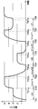
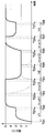
- Timing chart which shows the voltage of a capacitor when disconnection occurs in the 3rd signal wire between a 3rd input part and a multiplexer. It is a timing chart which shows the voltage of the capacitor in the normal state in the third embodiment. It is a timing chart which shows the voltage of the capacitor when the 2nd abnormality in a 3rd embodiment occurs. It is a timing chart which shows voltage of a capacitor when a 1st unusual occurs in a 3rd embodiment. It is a timing chart which shows the voltage of the capacitor when the 2nd abnormality in a 4th embodiment occurs. It is a timing chart which shows voltage of a capacitor when a 1st unusual occurs in a 4th embodiment. It is a figure which shows typically the AD conversion apparatus in other embodiment. It is a figure which shows typically the AD conversion apparatus in other embodiment. It is a figure which shows typically the AD conversion apparatus in other embodiment. It is a figure which shows typically the AD conversion apparatus in other embodiment.
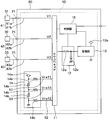
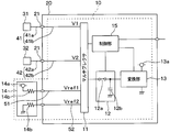
- the AD converter 10 of this embodiment is mounted on an IC (that is, integrated circuit) chip 20 as shown in FIG. 1, and external voltages of analog signals input from external input units 31 and 32 are
- the digital signal is configured to be AD converted.
- the first detection voltage V1 as an external voltage is input to the IC chip 20 from the first input portion 31, and the external voltage is output from the second input portion 32.
- the second detection voltage V2 is input will be described.
- detection voltages as external voltages may be input to the IC chip 20 from a plurality of input units.
- the AD converter 10 includes a multiplexer (ie, MPX) 11, a sample and hold (hereinafter simply referred to as S / H) circuit 12, a conversion unit 13, a reference voltage input unit 14, and a control unit 15. There is.
- MPX multiplexer
- S / H sample and hold
- the multiplexer 11 is connected to the first input portion 31 via the first signal line 41 and connected to the second input portion 32 via the second signal line 42.
- the first signal line 41 is a signal line 41 a such as a wire disposed between the connection terminal 21 of the IC chip 20 and the terminal of the first input unit 31, the connection terminal 21 and the inside of the IC chip 20.
- a signal line 41b such as a wiring pattern formed on the substrate.
- the second signal line 42 is formed in the signal line 42 a such as a wire disposed between the connection terminal 21 of the IC chip 20 and the terminal of the second input section 32, the connection terminal 21 and the IC chip 20.
- the signal line 42b such as the wiring pattern.
- the multiplexer 11 corresponds to a switching unit.
- the multiplexer 11 selects one input signal from the plurality of input signals input based on the control signal from the control unit 15 and outputs the selected input signal to the S / H circuit 12.
- the multiplexer 11 receives, as an input signal, the first detection voltage V1 from the first input unit 31 and the second detection voltage V2 from the second input unit 32. Further, although specifically described later, the multiplexer 11 receives the first reference voltage Vref1 from the reference voltage input unit 14 as the input signal and the second reference voltage Vref2.
- the first input unit 31 and the second input unit 32 are composed of various sensors such as a pressure sensor, a temperature sensor, an acceleration sensor, an angular velocity sensor, etc.
- a ground circuit connected to the In the present embodiment the ground circuit is configured to have a capacitor or the like disposed between the ground and the output terminal of each of the input units 31 and 32, and also functions as a filter circuit for reducing noise.
- a general filter circuit is used as the ground circuit.
- the S / H circuit 12 has a switch 12a connected between the multiplexer 11 and the conversion unit 13, and a capacitor 12b connected between the connection point between the switch 12a and the conversion unit 13 and the ground. doing.
- the switch 12 a When the switch 12 a is turned on, the S / H circuit 12 is connected to the multiplexer 11, and the capacitor 12 b is in a charge state based on the voltage input from the multiplexer 11. That is, the S / H circuit 12 holds the voltage input from the multiplexer 11 when the switch 12 a is turned on.
- the conversion unit 13 is configured to have a comparator or the like, and quantizes a voltage between the conversion reference voltage (for example, 5 V) applied from the reference power supply 13 a and the ground voltage (that is, a predetermined voltage) That is, it is configured to be able to be digitized. Then, the conversion unit 13 converts the voltage held by the S / H circuit 12 into a digital signal based on the control signal from the control unit 15, and outputs the digital signal to the control unit 15.
- the conversion reference voltage for example, 5 V
- the ground voltage that is, a predetermined voltage
- the reference voltage input unit 14 is configured to have a power supply 14 a, a resistor 14 b, and the like, and is connected to the multiplexer 11 via signal lines 51 and 52 such as wiring patterns and inputs a plurality of reference voltages to the multiplexer 11 .
- the reference voltage input unit 14 inputs the first reference voltage Vref1 to the multiplexer 11 through the signal line 51, and inputs the second reference voltage Vref2 through the signal line 52.
- the first reference voltage Vref1 is a value corresponding to the voltage of the power supply 14a
- the second reference voltage Vref2 is a ground voltage (that is, 0 V).
- the control unit 15 is a control circuit which includes, for example, a microcomputer, a storage unit such as a memory, and peripheral circuits thereof, and executes predetermined processing according to a program stored in the storage unit or the like.
- the control unit 15 is connected to the multiplexer 11, the S / H circuit 12, the conversion unit 13, an external circuit, and the like.
- the control unit 15 determines and changes the input signal selected by the multiplexer 11 by inputting a control signal to the multiplexer 11. Further, the control unit 15 switches the on state and the off state of the switch 12 a by inputting a control signal to the S / H circuit 12. Furthermore, the control unit 15 inputs a control signal to the conversion unit 13 to cause the conversion unit 13 to perform AD conversion and input the converted digital signal to the control unit 15. Then, when the digital signal is input from the conversion unit 13, the control unit 15 performs predetermined processing while storing the digital signal in the storage unit as needed. In the present embodiment, as one of the predetermined processes, the control unit 15 determines whether or not a break occurs in the first and second signal lines 41 and 42 between the multiplexer 11 and each of the input units 31 and 32. Execute the disconnection judgment of.
- the control unit 15 when the disconnection determination is performed, the control unit 15 does not allow the multiplexer 11 to select the detection voltage input through the signal line determined in the disconnection determination.
- a reference voltage different in value from the detection voltage is selected.
- the normal range of the first detection voltage V1 is 0 to 3 V
- the normal range of the second detection voltage V2 is 2 to 5 V
- the first reference voltage Vref1 is 5 V.
- the voltage Vref2 is set to 0V. Therefore, when the control unit 15 performs the disconnection determination of the first signal line 41, the first reference voltage Vref1 is selected before the multiplexer 11 selects the first detection voltage V1.
- the control unit 15 executes the disconnection determination of the second signal line 42, the second reference voltage Vref2 is selected before the multiplexer 11 selects the second detection voltage V2. Let's do it. Then, the control unit 15 determines whether or not the first signal line 41 is disconnected based on the digital signal corresponding to the first detection voltage V1 and the digital signal corresponding to the first reference voltage Vref1 (see FIG. Hereinafter, the first disconnection judgment is simply performed. In addition, the control unit 15 determines whether or not the second signal line 42 is disconnected based on the digital signal corresponding to the second detection voltage V2 and the digital signal corresponding to the second reference voltage Vref2 Hereinafter, the second disconnection judgment is simply performed.
- the normal range of the first detection voltage V1 is a possible range of the first detection voltage V1 and corresponds to a first predetermined range.
- the normal range of the second detection voltage V2 is a possible range of the second detection voltage V2, and corresponds to a second predetermined range.
- the normal range of the first detection voltage V1 is 0 to 3 V
- the normal range of the second detection voltage V2 is 2 to 5 V
- the first reference voltage Vref1 is 5 V
- the second reference voltage Vref2 is 0 V.
- the first detection voltage V1 when the first detection voltage V1 is selected by the multiplexer 11 is 3 V
- the second detection voltage V2 when the second detection voltage V2 is selected is An example of 2V will be described.
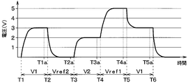
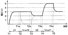
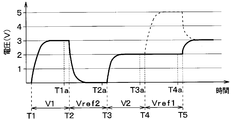
- 2A to 2C show the voltages selected by the multiplexer 11 during each time point. Then, for example, the following processing may be performed continuously and always, may be performed only when the IC chip 20 is activated, or may be performed every predetermined period. It is also good.
- the control unit 15 causes the multiplexer 11 to select the first detection voltage V1 at time T1, and turns on the switch 12a. Thereby, the charge based on the first detection voltage V1 is accumulated in the capacitor 12b, and the capacitor 12b becomes a voltage corresponding to the first detection voltage V1. Then, the control unit 15 turns off the switch 12a at time T1a, causes the conversion unit 13 to generate a digital signal based on the voltage of the capacitor 12b, and inputs the digital signal. Thereafter, predetermined processing using the digital signal is performed.
- the control unit 15 causes the multiplexer 11 to select the second reference voltage Vref2, and turns on the switch 12a.
- the first detection voltage V1 selected at time T1 is 3V
- the second reference voltage Vref2 is 0V.
- the accumulated charge is released from the ground of the reference voltage input unit 14, and the capacitor 12b becomes a voltage corresponding to the second reference voltage Vref2.
- the control unit 15 turns off the switch 12a, causes the conversion unit 13 to generate a digital signal based on the voltage of the capacitor 12b, and causes the digital signal to be input. Thereafter, predetermined processing using the digital signal is performed.
- the control unit 15 causes the multiplexer 11 to select the second detection voltage V2 and turns on the switch 12a. Thereby, the electric charge based on the 2nd detection voltage V2 is accumulate
- the capacitor 12b has a voltage corresponding to the second detection voltage V2.
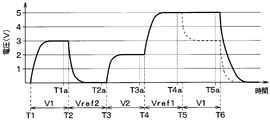
- the voltage of the capacitor 12b does not change. . That is, the digital signal generated at time point T2a and the digital signal generated at time point T3a become the same signal. Therefore, when the digital signal generated at the time point T2a and the digital signal generated at the time point T3a are the same signal, the control unit 15 determines that the second signal line 42 is disconnected. And outputs a control signal to notify an external circuit or the like of the occurrence of disconnection.
- the normal range of the second detection voltage V2 is 2 to 5 V
- the second reference voltage Vref2 is 0 V. Therefore, when no disconnection occurs in the second signal line 42, a digital signal having a value different from the digital signal is generated before the digital signal corresponding to the second detection voltage V2 is generated. . Therefore, the control unit 15 can easily execute the second disconnection determination by determining whether or not the digital signal generated at the time point T2a matches the digital signal generated at the time point T3a. Further, in the present embodiment, the second disconnection determination is performed by determining whether the digital signals coincide with each other. However, the determination is performed based on the second reference held by the capacitor 12 b of the S / H circuit 12. It can be said that the determination is based on the change in voltage between the voltage Vref2 and the second detection voltage V2.
- the same signal in the present specification means that they are substantially the same signal including the influence of a conversion error, a leak current, and the like.
- the coincidence of two digital signals in the present specification means that they substantially coincide including the effects of conversion error, leakage current, and the like. That is, when comparing the two digital signals, the control unit 15 adds the two digital signals when the change between the two digital signals is within a predetermined range, in addition to the case where the two digital signals completely match. It is determined that the two match. Then, when executing the disconnection determination, the control unit 15 determines that the disconnection occurs when the difference between the two digital signals is within the predetermined range.
- the second disconnection determination performed by the control unit 15 is performed when the voltage change between the second reference voltage Vref2 and the second detection voltage V2 held by the capacitor 12b of the S / H circuit 12 is within a predetermined range. It can be said that it is determined that the second signal line 42 is broken.
- the control unit 15 causes the multiplexer 11 to select the first reference voltage Vref1 and turns on the switch 12a at time T4.
- the second detection voltage V2 selected at time T3 is 2V
- the first reference voltage Vref1 is 5V. Therefore, the charge based on the voltage of the first reference voltage Vref1 is accumulated in the capacitor 12b, and the capacitor 12b has a voltage corresponding to the first reference voltage Vref1.
- the control unit 15 turns off the switch 12a at time point T4a, causes the conversion unit 13 to generate a digital signal based on the voltage of the capacitor 12b, and inputs the digital signal. Thereafter, predetermined processing using the digital signal is performed.
- the control unit 15 causes the multiplexer 11 to select the first detection voltage V1 and turns on the switch 12a.
- the first detection voltage V1 selected at time T5 is 3V
- the first reference voltage Vref1 is 5V. Therefore, in the capacitor 12b, a part of the accumulated charge is released from the ground in the ground circuit in the first input unit 31, and becomes a voltage corresponding to the first detection voltage V1.
- the control unit 15 turns off the switch 12a at time T5a, causes the conversion unit 13 to generate a digital signal based on the voltage of the capacitor 12b, and inputs the digital signal. Thereafter, predetermined processing using the digital signal is performed. Specifically, at this time, the control unit 15 executes the first disconnection determination as one of the predetermined processes.
- the capacitor 12b has a voltage corresponding to the first detection voltage V1.
- the voltage of the capacitor 12b does not change even if the multiplexer 11 selects the first detection voltage V1 as shown in FIG. 2C. . That is, the digital signal generated at time point T4a and the digital signal generated at time point T5a become the same signal. Therefore, when the digital signal generated at the time point T4a and the digital signal generated at the time point T5a are the same signal, the control unit 15 determines that the first signal line 41 is broken. And outputs a control signal to notify an external circuit or the like of the occurrence of an abnormality.
- FIG. 2C shows the voltage of the capacitor 12b when a break occurs in the first signal line 41 between time point T2 and time point T5.
- the normal range of the first detection voltage V1 is 0 to 3 V, and the first reference voltage Vref1 is 5 V. Therefore, when no disconnection occurs in the first signal line 41, a digital signal having a value different from that of the digital signal is generated before the digital signal corresponding to the first detection voltage V1 is generated. . Therefore, the control unit 15 can easily execute the first disconnection determination by determining whether or not the digital signal generated at the time point T4a matches the digital signal generated at the time point T5a. Further, in the present embodiment, the first disconnection determination is performed by determining whether or not the digital signals coincide with each other. However, the determination is made based on the first reference held by the capacitor 12b of the S / H circuit 12.
- the determination is based on the presence or absence of a change in voltage between the voltage Vref1 and the first detection voltage V1. Then, the control unit 15 executes the first disconnection determination as described above. Therefore, the first disconnection determination is performed when the voltage change between the first reference voltage Vref1 and the first detection voltage V1 held by the capacitor 12b of the S / H circuit 12 is within the predetermined range. It can be said that it is determined that a break has occurred in the
- control unit 15 After that, the control unit 15 performs the same processing as that after time T2 after time T6.
- the multiplexer 11 before causing the multiplexer 11 to select the detection voltage input through the signal line determined by the disconnection determination, the multiplexer 11 selects the reference voltage having a value different from the detection voltage. ing. And disconnection determination is performed based on the presence or absence of the change of the voltage hold
- the first reference voltage Vref1 has a value different from the normal range of the first detection voltage V1
- the second reference voltage Vref2 has a value different from the normal range of the second detection voltage V2. It is like that.
- the control unit 15 causes the multiplexer 11 to select the first reference voltage Vref1 before the first detection voltage V1. For this reason, the control unit 15 easily performs the first disconnection determination by determining whether the digital signal corresponding to the first detection voltage V1 matches the digital signal corresponding to the first reference voltage Vref1. be able to.
- 0 V can be included as a normal range of the first detection voltage V1, and the application range can be expanded.
- the control unit 15 when the second disconnection determination is performed, the control unit 15 causes the multiplexer 11 to select the second reference voltage Vref2 before the second detection voltage V2. Therefore, the control unit 15 can easily perform the second disconnection determination by determining whether the digital signal corresponding to the second detection voltage V2 matches the digital signal corresponding to the second reference voltage Vref2. Can. By performing the second disconnection determination in this manner, 5 V can be included as a normal range of the second detection voltage V2 in addition to the above range.
- the present embodiment is also applicable to the case where three or more detection voltages are input to the AD converter 10.
- the reference voltages may be appropriately added and adjusted in accordance with the normal range of each detection voltage.
- the control unit 15 causes the multiplexer 11 to select a reference voltage having a value different from the normal range of the detection voltage before each detection voltage, and compares the digital signal of the detection voltage with the digital signal of the reference voltage. Therefore, the disconnection determination may be performed.
- the present embodiment is the one in which the configuration of the AD conversion device 10 is modified from the first embodiment, and the other parts are the same as the first embodiment, and thus the description thereof is omitted here.
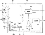
- the multiplexer 11 is connected to the third input unit 33 via the third signal line 43 together with the first input unit 31 and the second input unit 32.
- the third signal line 43 has the same configuration as the first and second signal lines 41 and 42. That is, the third signal line 43 is formed in the signal line 43 a such as a wire disposed between the connection terminal 21 of the IC chip 20 and the terminal of the third input unit 33, the connection terminal 21 and the IC chip 20. And a signal line 43b such as a wiring pattern.
- the multiplexer 11 receives the third detection voltage V3 from the third input unit 33 together with the first detection voltage V1 and the second detection voltage V2.
- the normal value of the third detection voltage V3 is 0V or 5V. That is, the normal value of the third detection voltage V3 is made equal to the first reference voltage Vref1 or the second reference voltage Vref2.
- the third detection voltage V3 corresponds to a third external voltage
- 5 V corresponds to a first voltage
- 0 V corresponds to a second voltage.
- the reference voltage input unit 14 is configured to input the third reference voltage Vref3 through the signal line 53 to the multiplexer 11 in addition to the first reference voltage Vref1 and the second reference voltage Vref2.
- the third reference voltage Vref3 is a voltage obtained by dividing the voltage of the power supply 14a, and is about 2.5V. That is, the third reference voltage Vref3 is a value between possible values of the third detection voltage V3.
- the control unit 15 has the same configuration as that of the first embodiment, but in the present embodiment, a disconnection occurs in the third signal line 43 between the third input unit 33 and the multiplexer 11.
- a third disconnection determination (hereinafter also referred to simply as a third disconnection determination) as to whether or not there is present is performed.
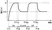
- FIGS. 4A and 4B showing the voltage of the capacitor 12b.
- the operation of the control unit 15 with respect to the first detection voltage V1, the second detection voltage V2, the first reference voltage Vref1, and the second reference voltage Vref2 is the same as that of the first embodiment, and hence the third detection voltage is described below. Only the relationship between V3 and the third reference voltage Vref3 will be described. In the following, an example in which the third detection voltage V3 is 5 V when the third detection voltage V3 is selected by the multiplexer 11 will be described. 4A and 4B show the voltage selected by the multiplexer 11 during each time point.
- the control unit 15 causes the multiplexer 11 to select the third detection voltage V3 and turns on the switch 12a. Thereby, the charge based on the third detection voltage V3 is accumulated in the capacitor 12b, and the capacitor 12b becomes a voltage corresponding to the third detection voltage V3. Then, at time T11a, the control unit 15 turns off the switch 12a, causes the conversion unit 13 to generate a digital signal based on the voltage of the capacitor 12b, and causes the digital signal to be input. Thereafter, predetermined processing using the digital signal is performed.
- the control unit 15 causes the multiplexer 11 to select the third reference voltage Vref3 and turns on the switch 12a.
- the capacitor 12b discharges the accumulated charge from the ground of the reference voltage input unit 14
- the third reference voltage Vref3 is obtained.
- the control unit 15 turns off the switch 12a, causes the conversion unit 13 to generate a digital signal based on the voltage of the capacitor 12b, and causes the digital signal to be input. Thereafter, predetermined processing using the digital signal is performed.
- the control unit 15 causes the multiplexer 11 to select the third detection voltage V3 and turns on the switch 12a.
- the third detection voltage V3 selected at time T13 is 5V
- the third reference voltage Vref3 is 2.5V. Therefore, when no disconnection occurs in the third signal line 43, charges corresponding to the third detection voltage V3 are accumulated in the capacitor 12b, and the capacitor 12b becomes a voltage corresponding to the third detection voltage V3.
- the control unit 15 turns off the switch 12a at time T13a, causes the conversion unit 13 to generate a digital signal based on the voltage of the capacitor 12b, and inputs the digital signal. Thereafter, predetermined processing using the digital signal is performed. Specifically, at this point, the control unit 15 executes the third disconnection determination as one of the predetermined processes.
- the capacitor 12b has a voltage corresponding to the third detection voltage V3.
- the voltage of the capacitor 12b does not change. . That is, the digital signal generated at time T12a and the digital signal generated at time T13a become the same signal. Therefore, when the digital signal generated at time T12a and the digital signal generated at time T13a are the same signal, the control unit 15 determines that the third signal line 43 is broken. And outputs a control signal to notify an external circuit or the like of the occurrence of an abnormality.
- FIG. 4B shows the voltage of the capacitor 12b when a break occurs in the third signal line 43 between time point T12 and time point T13.
- the normal value of the third detection voltage V3 is 0V or 5V
- the third reference voltage Vref3 is 2.5V. Therefore, when no disconnection occurs in the third signal line 43, a digital signal having a value different from that of the digital signal is generated before the digital signal corresponding to the third detection voltage V3 is generated. . Therefore, the control unit 15 can easily execute the third disconnection determination by determining whether the digital signal generated at the time T12a and the digital signal generated at the time T13a coincide with each other. Further, in the present embodiment, the third disconnection determination is performed by determining whether or not the digital signals coincide with each other. However, the determination is performed based on the third criterion held by the capacitor 12b of the S / H circuit 12.
- the determination is based on the presence or absence of a change in voltage between the voltage Vref3 and the third detection voltage V3.
- the control part 15 is performing 3rd disconnection determination as mentioned above. Therefore, the third disconnection determination is performed when the voltage change between the third reference voltage Vref3 and the third detection voltage V3 held by the capacitor 12b of the S / H circuit 12 is within the predetermined range. It can be said that it is determined that a break has occurred in the
- control unit 15 performs the same processing as that after time T12 after time T14.
- the third detection voltage V3 to be selected is 5 V
- the same applies to the case in which the third detection voltage to be selected is 0 V.
- the third detection voltage V3 which is one of two voltages is input through the third signal line 43, and the third reference voltage Vref3 is the third 3 is different from the detection voltage V3. Then, when the third disconnection determination is performed, the control unit 15 causes the multiplexer 11 to select the third reference voltage Vref3 before the third detection voltage V3. Therefore, the control unit 15 easily performs the third disconnection determination by determining whether or not the digital signal corresponding to the third detection voltage V3 matches the digital signal corresponding to the third reference voltage Vref3. be able to.
- disconnection determination of the third signal line 43 to which the third detection voltage V3 which is one of the two voltages is input can also be executed, and the applicable range of the detection voltage can be expanded. .
- the third reference voltage Vref3 has a value different from that of the third detection voltage V3 and is a value between the first reference voltage Vref1 and the second reference voltage Vref2. Therefore, the resistor 14b may be appropriately added to the reference voltage input unit 14 that generates the first reference voltage Vref1 and the second reference voltage Vref2, and the circuit can be prevented from being complicated.
- an abnormality determination as to whether or not an abnormality has occurred in the reference voltage input unit 14 can also be performed with respect to the first embodiment, and the other respects are the same as in the first embodiment. The description is omitted here because it is present.
- the AD converter 10 of this embodiment has the same configuration as that of the first embodiment.
- the control unit 15 of the present embodiment performs abnormality determination including whether or not an abnormality has occurred in the reference voltage input unit 14.
- the abnormality in the reference voltage input unit 14 here is a break in the signal lines 51 and 52 connecting the reference voltage input unit 14 and the multiplexer 11.
- the case is included. That is, the occurrence of abnormality in the reference voltage input unit 14 here means that a failure has occurred in the reference voltage input unit 14 and that a break has occurred in the signal lines 51 and 52. It means that at least one of them is occurring.
- the occurrence of at least one of the failure in the reference voltage input unit 14 and the disconnection of the signal line 51 is also referred to as a first abnormality, and it is determined whether the first abnormality has occurred or not. 1 It is also called an abnormality judgment.
- the occurrence of at least one of a failure in the reference voltage input unit 14 and a break in the signal line 52 is also referred to as a second abnormality, and it is determined whether a second abnormality has occurred or not. It is also called an abnormality judgment.
- the normal range of the first detection voltage V1 is 0 to 3 V
- the normal range of the second detection voltage V2 is 2 to 5 V
- the first reference voltage Vref1 is 5 V.
- the second reference voltage Vref2 will be described as being 0V.
- the first detection voltage V1 when the first detection voltage V1 is selected by the multiplexer 11 is 3V
- the second detection voltage V2 when the second detection voltage V2 is selected is 2V.
- 5A to 5C show voltages selected by the multiplexer 11 during each time point.
- control unit 15 performs the same process as at time T1, and at time T21a, performs the same process as time T1a.
- the control unit 15 causes the multiplexer 11 to select the first reference voltage Vref1, and turns on the switch 12a.
- the first detection voltage V1 selected at time T21 is 3V
- the first reference voltage Vref1 is 5V. Therefore, the charge based on the voltage of the first reference voltage Vref1 is accumulated in the capacitor 12b, and the capacitor 12b has a voltage corresponding to the first reference voltage Vref1.
- the control unit 15 turns off the switch 12a, causes the conversion unit 13 to generate a digital signal based on the charge accumulated in the capacitor, and causes the digital signal to be input. Thereafter, predetermined processing using the digital signal is performed.
- the control unit 15 causes the multiplexer 11 to select the second reference voltage Vref2, and turns on the switch 12a.
- the first reference voltage Vref1 selected at time T22 is 5V
- the second reference voltage Vref2 is 0V.
- the control unit 15 turns off the switch 12a at time T23a, causes the conversion unit 13 to generate a digital signal based on the voltage of the capacitor 12b, and inputs the digital signal.
- predetermined processing using the digital signal is performed. Specifically, at this time, the control unit 15 executes the second abnormality determination as one of the predetermined processes.
- the capacitor 12b has a voltage corresponding to the second reference voltage Vref2.
- the voltage of the capacitor 12b does not change. That is, the digital signal generated at time T22a and the digital signal generated at time T23a become the same signal. Therefore, when the digital signal generated at time T22a and the digital signal generated at time T23a are the same signal, the control unit 15 determines that the second abnormality has occurred, and the external circuit or the like Outputs a control signal to notify that the second abnormality has occurred.
- the normal range of the first detection voltage V1 is 0 to 3 V
- the second reference voltage Vref2 is 0 V. Therefore, immediately after the first detection voltage V1, the second reference voltage Vref2 is converted into a digital signal, and the digital signal corresponding to the first detection voltage V1 is compared with the digital signal corresponding to the second reference voltage Vref2. If so, the second abnormality determination may not be possible. That is, when 0 V is input as the first detection voltage V1, the first detection voltage V1 and the second reference voltage Vref2 become the same, and it can not be determined whether the second abnormality occurs. Therefore, in the present embodiment, the first reference voltage Vref1 is converted to a digital signal before the second reference voltage Vref2.
- the control unit 15 can easily execute the second abnormality determination by determining whether the digital signal generated at the time point T22a and the digital signal generated at the time point T23a coincide with each other. Further, in the present embodiment, the second abnormality determination is performed by determining whether the digital signals coincide with each other, but the determination is made based on the first reference held by the capacitor 12 b of the S / H circuit 12. It can be said that this determination is based on the presence or absence of a change in voltage between the voltage Vref1 and the second reference voltage Vref2. And the control part 15 is performing 2nd abnormality determination as mentioned above.
- the second abnormality occurs when the voltage change between the first reference voltage Vref1 and the second reference voltage Vref2 held by the capacitor 12b of the S / H circuit 12 is within a predetermined range. It can be said that it is determined that the
- control unit 15 performs processing similar to that at time T3 at time T24, and performs processing similar to that at time T3a at time T24a.
- the control unit 15 causes the multiplexer 11 to select the second reference voltage Vref2, and turns on the switch 12a.
- the second detection voltage V2 selected at time T24 is 2V
- the second reference voltage Vref2 is 0V.
- the control unit 15 turns off the switch 12a at time T25a, causes the conversion unit 13 to generate a digital signal based on the voltage of the capacitor 12b, and inputs the digital signal. Thereafter, predetermined processing using the digital signal is performed.
- the control unit 15 causes the multiplexer 11 to select the first reference voltage Vref1, and turns on the switch 12a. Thereby, the charge based on the first reference voltage Vref1 is accumulated in the capacitor 12b, and the capacitor 12b becomes a voltage corresponding to the first reference voltage Vref1. Then, the control unit 15 turns off the switch 12a at time T26a, causes the conversion unit 13 to generate a digital signal based on the voltage of the capacitor 12b, and inputs the digital signal. Thereafter, predetermined processing using the digital signal is performed. Specifically, at this time, the control unit 15 executes the first abnormality determination as one of the predetermined processes.
- the capacitor 12b has a voltage corresponding to the first reference voltage Vref1.
- the voltage of the capacitor 12b does not change. That is, the digital signal generated at time T25a and the digital signal generated at time T26a become the same signal. Therefore, when the digital signal generated at time T25a and the digital signal generated at time T26a are the same signal, the control unit 15 determines that the first abnormality has occurred, and the external circuit or the like Output a control signal to notify the error occurrence.
- FIG. 5C shows the voltage of the capacitor 12b when the first abnormality occurs between time point T23 and time point T26.
- the normal range of the second detection voltage V2 is 2 to 5 V
- the first reference voltage Vref1 is 5 V. Therefore, immediately after the second detection voltage V2, the first reference voltage Vref1 is converted to a digital signal, and the digital signal corresponding to the second detection voltage V2 is compared with the digital signal corresponding to the first reference voltage Vref1. If this is the case, the first abnormality determination may not be possible. That is, when 5 V is input as the second detection voltage V2, the second detection voltage V2 and the first reference voltage Vref1 become the same, and it can not be determined whether or not the first abnormality occurs.
- the second reference voltage Vref2 is converted to a digital signal before the first reference voltage Vref1. Then, when the first abnormality does not occur, a digital signal different from the digital signal is generated before the first reference voltage Vref1 is converted into the digital signal.
- the control unit 15 can easily execute the first abnormality determination by determining whether the digital signal generated at the time point T25a matches the digital signal generated at the time point T26a. Further, in the present embodiment, the first disconnection determination is performed by determining whether or not the digital signals coincide with each other. However, the determination is performed based on the second reference held by the capacitor 12b of the S / H circuit 12.
- the determination is based on the presence or absence of a change in voltage between the voltage Vref2 and the first reference voltage Vref1. Then, the control unit 15 executes the first abnormality determination as described above. Therefore, in the first abnormality determination, the first abnormality occurs when the voltage change between the second reference voltage Vref2 and the first reference voltage Vref1 held by the capacitor 12b of the S / H circuit 12 is within a predetermined range. It can be said that it is determined that the
- control unit 15 performs processing similar to that at time T5 at time T27, and performs processing similar to that at time T5a at time T27a. Thereafter, the control unit 15 performs the same processing as that after time T22 after time T28.
- the abnormality of the AD converter 10 can be determined with higher accuracy.
- the multiplexer 11 selects the second reference voltage Vref2 before the first reference voltage Vref1. Further, when the second abnormality determination is performed, the control unit 15 causes the multiplexer 11 to select the first reference voltage Vref1 before the second reference voltage Vref2. Therefore, the control unit 15 can easily determine the first abnormality and the second abnormality by determining whether the digital signal corresponding to the first reference voltage Vref1 matches the digital signal corresponding to the second reference voltage Vref2. Abnormality determination can be performed.
- control unit 15 changes the order of the voltages selected by the multiplexer 11 to perform the first abnormality determination and the second abnormality determination. That is, in the present embodiment, it is not necessary to add a new circuit to perform the first abnormality determination and the second abnormality determination. Therefore, in the present embodiment, the first abnormality determination and the second abnormality determination can be executed while suppressing an increase in circuit scale.
- This embodiment changes the normal range of the first detection voltage V1 and the second detection voltage V2 with respect to the first embodiment, and further performs the first abnormality determination and the second abnormality determination as in the third embodiment. It is intended to The other aspects are the same as in the first embodiment, and thus the description thereof is omitted here.
- the AD converter 10 of this embodiment has the same configuration as that of the first embodiment.
- the normal range of the first detection voltage V1 is 1 to 3 V
- the normal range of the second detection voltage V2 is 2 to 4 V. That is, the first reference voltage Vref1 and the second reference voltage Vref2 have different values from the first detection voltage V1 and the second detection voltage V2, respectively.
- the normal range of the first detection voltage V1 is 1 to 3 V
- the normal range of the second detection voltage V2 is 2 to 4 V
- the first reference voltage Vref1 is 5 V
- the second reference voltage Vref2 is 0V.
- the first detection voltage V1 when the first detection voltage V1 is selected by the multiplexer 11 is 3 V
- the second detection voltage V2 when the second detection voltage V2 is selected is An example of 2V will be described.
- 6A and 6B show the voltages selected by the multiplexer 11 during each time point.
- control unit 15 of the present embodiment is basically the same as that described in the first embodiment. Then, at time T2a, the control unit 15 executes the second abnormality determination as one of the predetermined processes.
- the capacitor 12b changes from time T2 to a voltage according to the second reference voltage Vref2.
- the second reference voltage Vref2 is selected by the multiplexer 11
- the voltage of the capacitor 12b does not change. That is, the digital signal generated at time point T1a and the digital signal generated at time point T2a become the same signal. Therefore, when the digital signal generated at the time point T1a and the digital signal generated at the time point T2a are the same signal, the control unit 15 determines that the second abnormality has occurred, and the external circuit etc. Output a control signal to notify the error occurrence.
- the normal range of the first detection voltage V1 is 1 to 3 V
- the second reference voltage Vref2 is 0 V. Therefore, when the second abnormality does not occur, the digital signal having a value different from the digital signal is generated before the digital signal corresponding to the second reference voltage Vref2 is generated. Therefore, the control unit 15 can easily execute the second abnormality determination by determining whether or not the digital signal generated at the time point T1a matches the digital signal generated at the time point T2a. And the control part 15 is performing 2nd abnormality determination as mentioned above.
- the second abnormality occurs when the voltage change between the first detection voltage V1 and the second reference voltage Vref2 held by the capacitor 12b of the S / H circuit 12 is within a predetermined range. It can be said that it is determined that the
- control unit 15 executes the first abnormality determination as one of the predetermined processes.
- control unit 15 determines that the first abnormality has occurred, and the external circuit or the like Output a control signal to notify the error occurrence.
- the normal range of the second detection voltage V2 is 2 to 4 V
- the first reference voltage Vref1 is 5 V. Therefore, when the first abnormality does not occur, a digital signal having a value different from that of the digital signal is generated before the digital signal corresponding to the first reference voltage Vref1 is generated. Therefore, the control unit 15 can easily execute the first abnormality determination by determining whether the digital signal generated at the time point T3a matches the digital signal generated at the time point T4a. Then, the control unit 15 executes the first abnormality determination as described above.
- the first abnormality occurs when the voltage change between the second detection voltage V2 held by the capacitor 12b of the S / H circuit 12 and the first reference voltage Vref1 is within a predetermined range. It can be said that it is determined that the
- the first reference voltage Vref1 and the second reference voltage Vref2 have different values from the first detection voltage V1 and the second detection voltage V2. Therefore, even if the second detection voltage V2 is selected by the multiplexer 11 before the first reference voltage Vref1, the digital signal according to the first reference voltage Vref1 and the digital signal according to the second detection voltage V2 Are different values. That is, the second detection voltage V2 used in the second disconnection determination can be used as it is. Similarly, even if the first detection voltage V1 is selected by the multiplexer 11 before the second reference voltage Vref2, a digital signal corresponding to the second reference voltage Vref2 and a digital signal corresponding to the first detection voltage V1 are used. Are different values. That is, the first detection voltage V1 used in the first disconnection determination can be used as it is.
- the second reference voltage Vref2 does not have to be selected by the multiplexer 11 to perform the first abnormality determination, and the first abnormality determination is performed.
- the reference voltage Vref1 does not have to be selected by the multiplexer 11. Therefore, according to the present embodiment, it is possible to shorten the total period required to perform all the determinations of the first disconnection determination, the second disconnection determination, the first abnormality determination, and the second abnormality determination.
- the first reference voltage Vref1 and the second reference voltage Vref2 have different values from the first detection voltage V1 and the second detection voltage V2. Therefore, even if the first reference voltage Vref1 is converted before the second detection voltage V2, the second detection voltage V2 and the first reference voltage Vref1 have different values. Therefore, the first reference voltage Vref1 may be converted before the second detection voltage V2. Similarly, the second reference voltage Vref2 may be converted before the first detection voltage V1.
- the multiplexer 11, the S / H circuit 12, the conversion unit 13, the reference voltage input unit 14, and the control unit 15 may not be mounted on the common IC chip 20.
- the reference voltage input unit 14 may not be mounted on the IC chip 20 but may be mounted on another chip. .
- the reference voltage input unit 14 may not be mounted on the IC chip 20.
- control unit 15 is not mounted on the IC chip 20, and a vehicle ECU (ie, An Engine Control Unit) may perform the function of the control unit 15 of each of the above embodiments.
- a vehicle ECU ie, An Engine Control Unit
- a plurality of control units 15 may be provided, and each control unit 15 may perform the above functions.
- a control unit that controls the multiplexer 11, a control unit that controls the S / H circuit 12, and a control unit that controls the conversion unit 13 may be separately provided.
- the conversion reference voltage is input from the reference power supply 13a to the conversion unit 13.
- the conversion unit 13 does not include the reference power supply 13a.
- a reference voltage may be input. According to this, the number of parts can be reduced, and the circuit scale can be further reduced.
- the control unit 15 uses the reference voltage input from the reference voltage input unit 14, and when the conversion unit 13 generates a digital signal according to the reference voltage, based on the digital signal, The abnormality determination of the conversion unit 13 may be performed. That is, the reference voltage input from the reference voltage input unit 14 may be used for another application.
- the reference voltage generation unit that generates the reference voltage for performing the abnormality determination of the conversion unit 13 may have a function as the reference voltage input unit 14 of each of the above embodiments. According to this, it is possible to improve the function while suppressing an increase in the number of parts.
- control unit 15 may directly read the voltage of the capacitor 12b and perform each determination based on the presence or absence of a change in the voltage of the capacitor 12b. Even when the determination is performed in this manner, it is determined that disconnection or abnormality occurs when the change in the voltage of the capacitor 12b is within a predetermined range in consideration of a detection error or the like. Is preferred.
- the resistor 14 b may not be disposed between the power supply 14 a and the multiplexer 11. Similarly, as shown in FIG. 9, the resistor 14 b may not be disposed between the ground of the reference voltage input unit 14 and the multiplexer 11. Although not particularly illustrated, the same applies to the second embodiment.
- the above embodiments may be combined as appropriate.
- the second embodiment may be combined with the third and fourth embodiments, and the third detection voltage V3 may be input from the third input unit 33.
- the storage medium or memory is a non-transitional tangible storage medium.
Landscapes
- Engineering & Computer Science (AREA)
- Theoretical Computer Science (AREA)
- Testing Of Short-Circuits, Discontinuities, Leakage, Or Incorrect Line Connections (AREA)
- Analogue/Digital Conversion (AREA)
Abstract
複数の入力部(31、32)と信号線(41、42)を介して接続されて外部電圧(V1、V2)が入力されると共に、外部電圧(V1、V2)を選択して出力する切替部(11)と、切替部(11)の出力に応じた電圧を保持するS/H回路(12)と、S/H回路(12)で保持された電圧に基づいてAD変換する変換部(13)と、切替部(11)にて選択される外部電圧を決定すると共に、信号線(41、42)に断線が発生しているか否かの断線判定を実行する制御部(15)とを備える。制御部(15)に、断線判定では、判定される信号線(41、42)を通じて入力される外部電圧(V1、V2)を切替部(11)に選択させる前に外部電圧と異なる値とされた基準電圧(Vref1、Vref2)を切替部(11)に選択させ、外部電圧を選択させた後、S/H回路(12)で保持される基準電圧と外部電圧との電圧の変化に基づいて断線判定を行わせる。
Description
本出願は、2017年9月20日に出願された日本特許出願番号2017-180510号に基づくもので、ここにその記載内容が参照により組み入れられる。
本開示は、切替部と入力部との間の信号線に断線が発生しているか否かの断線判定を実行できるアナログ-デジタル(以下では、単にADともいう)変換装置に関する。
従来より、複数の入力部から入力されるアナログ信号である入力信号を順に選択しながらAD変換するAD変換装置が提案されている(例えば、特許文献1参照)。具体的には、このAD変換装置では、複数の入力部と信号線を介して接続される切替部としてのマルチプレクサを有しており、当該マルチプレクサで複数の入力部から入力される複数の入力信号から1つの入力信号が選択される。そして、マルチプレクサで選択された入力信号が変換部にてAD変換される。また、上記AD変換装置では、マルチプレクサと各入力部との間の信号線に、それぞれ断線検出用のプルダウン抵抗が備えられている。
なお、マルチプレクサと各入力部との間の信号線は、マルチプレクサが搭載されるチップの端子と入力部の端子とを接続するワイヤ等の信号線、およびチップの端子とマルチプレクサとを接続する配線パターン等の信号線を有して構成されている。
なお、マルチプレクサと各入力部との間の信号線は、マルチプレクサが搭載されるチップの端子と入力部の端子とを接続するワイヤ等の信号線、およびチップの端子とマルチプレクサとを接続する配線パターン等の信号線を有して構成されている。
しかしながら、上記AD変換装置では、マルチプレクサと各入力部とを接続する信号線の断線を検出するためには、それぞれの信号線にプルダウン抵抗を備える必要があり、回路規模が大型化してしまう。特に、マルチプレクサに多数の入力部を接続する場合には、各信号線にそれぞれプルダウン抵抗を備えることにより、回路規模の大型化が顕著になる。
本開示は、回路規模の縮小化を図りつつ、信号線に断線が発生しているか否かを検出することができるAD変換装置を提供することを目的とする。
本開示の1つの観点によれば、AD変換装置は、複数の入力部と信号線を介して接続され、複数の入力部からそれぞれアナログ信号である外部電圧が入力されると共に、複数の外部電圧から1つの外部電圧を選択して出力する切替部と、切替部から出力される外部電圧に応じた電圧を保持するサンプルホールド回路と、サンプルホールド回路で保持された電圧に基づいてAD変換する変換部と、切替部にて選択される外部電圧を決定すると共に、信号線に断線が発生しているか否かの断線判定を実行する制御部と、を備える。そして、AD変換装置は、切替部と接続され、切替部に所定の基準電圧を入力する基準電圧入力部を有する。制御部は、断線判定では、当該断線判定にて判定される信号線を通じて入力される外部電圧を切替部に選択させる前に、外部電圧と異なる値とされた基準電圧を切替部に選択させ、外部電圧を選択させた後、サンプルホールド回路で保持される基準電圧と外部電圧との電圧の変化の有無に基づき、電圧の変化が所定範囲内である場合に信号線に断線が発生していると判定するようにする。
これによれば、サンプルホールド回路で保持される電圧の変化の有無に基づいて断線判定を実行する。このため、各信号線にプルダウン抵抗を備える必要がなく、回路規模の縮小化を図ることができる。
本開示の別の観点によれば、切替部には、複数の入力部の1つである第1入力部から第1所定範囲内の第1外部電圧が入力されると共に、複数の入力部の1つである第2入力部から第2所定範囲内の第2外部電圧が入力され、さらに、基準電圧入力部から第1所定範囲内の値と異なる値とされた第1基準電圧、および第2所定範囲と異なる値であって、第1基準電圧と異なる値とされた第2基準電圧が入力されるようにする。制御部は、断線判定では、切替部にて、第1外部電圧が選択される前に第1基準電圧が選択されるようにし、第1外部電圧を選択させた後、サンプルホールド回路で保持される第1基準電圧と第1外部電圧との電圧の変化の有無に基づき、当該電圧の変化が所定範囲内である場合に第1入力部と切替部との間の信号線に断線が発生していると判定する第1断線判定と、切替部にて、第2外部電圧が選択される前に第2基準電圧が選択されるようにし、第2外部電圧を選択させた後、サンプルホールド回路で保持される第2基準電圧と第2外部電圧との電圧の変化の有無に基づき、当該電圧の変化が所定範囲内である場合に第2入力部と切替部との間の信号線に断線が発生していると判定する第2断線判定と、を行うようにする。
これによれば、第1断線判定では、異なる値となる第1基準電圧、第1外部電圧が順に切替部にて選択される。このため、制御部は、サンプルホールド回路で保持される電圧の変化の有無に基づき、容易に第1断線判定を実行できる。また、第2断線判定では、異なる値となる第2基準電圧、第2外部電圧が順に切替部にて選択される。このため、制御部は、サンプルホールド回路で保持される電圧の変化の有無に基づき、容易に第2断線判定を実行できる。
なお、各構成要素等に付された括弧付きの参照符号は、その構成要素等と後述する実施形態に記載の具体的な構成要素等との対応関係の一例を示すものである。
以下、本開示の実施形態について図に基づいて説明する。なお、以下の各実施形態相互において、互いに同一もしくは均等である部分には、同一符号を付して説明を行う。
(第1実施形態)
第1実施形態について説明する。本実施形態のAD変換装置10は、図1に示されるように、IC(すなわち、integrated circuit)チップ20に搭載されており、外部の入力部31、32から入力されるアナログ信号の外部電圧をデジタル信号にAD変換するように構成されている。なお、本実施形態では、理解を容易にするため、ICチップ20に、第1入力部31から外部電圧としての第1検出電圧V1が入力されると共に、第2入力部32から外部電圧としての第2検出電圧V2が入力される場合について説明する。但し、ICチップ20には、さらに複数の入力部からそれぞれ外部電圧としての検出電圧が入力されるようにしてもよい。
第1実施形態について説明する。本実施形態のAD変換装置10は、図1に示されるように、IC(すなわち、integrated circuit)チップ20に搭載されており、外部の入力部31、32から入力されるアナログ信号の外部電圧をデジタル信号にAD変換するように構成されている。なお、本実施形態では、理解を容易にするため、ICチップ20に、第1入力部31から外部電圧としての第1検出電圧V1が入力されると共に、第2入力部32から外部電圧としての第2検出電圧V2が入力される場合について説明する。但し、ICチップ20には、さらに複数の入力部からそれぞれ外部電圧としての検出電圧が入力されるようにしてもよい。
AD変換装置10は、マルチプレクサ(すなわち、MPX)11と、サンプルホールド(以下では、単にS/Hという)回路12と、変換部13と、基準電圧入力部14と、制御部15とを備えている。
マルチプレクサ11は、第1入力部31と第1信号線41を介して接続されていると共に、第2入力部32と第2信号線42を介して接続されている。本実施形態では、第1信号線41は、ICチップ20の接続端子21と第1入力部31の端子との間に配置されるワイヤ等の信号線41aと、接続端子21とICチップ20内に形成された配線パターン等の信号線41bとを有する構成とされている。同様に、第2信号線42は、ICチップ20の接続端子21と第2入力部32の端子との間に配置されるワイヤ等の信号線42aと、接続端子21とICチップ20内に形成された配線パターン等の信号線42bとを有する構成とされている。なお、本実施形態では、マルチプレクサ11が切替部に相当している。
そして、マルチプレクサ11は、制御部15からの制御信号に基づき、入力される複数の入力信号の中から1つの入力信号を選択し、S/H回路12へと出力する。本実施形態では、マルチプレクサ11には、入力信号として、第1入力部31から第1検出電圧V1が入力されると共に第2入力部32から第2検出電圧V2が入力される。また、マルチプレクサ11には、具体的には後述するが、入力信号として、基準電圧入力部14から第1基準電圧Vref1が入力されると共に第2基準電圧Vref2が入力される。
なお、本実施形態では、第1入力部31および第2入力部32は、圧力センサ、温度センサ、加速度センサ、角速度センサ等の各種センサ等で構成されており、特に図示しないが、内部にグランドと接続される接地回路を有している。本実施形態では、接地回路は、グランドと各入力部31、32の出力端子との間に配置されたコンデンサ等を有する構成とされており、ノイズを軽減するためのフィルタ回路としても機能する。言い換えると、本実施形態では、一般的なフィルタ回路を接地回路として利用している。
S/H回路12は、マルチプレクサ11と変換部13との間に接続されるスイッチ12aと、スイッチ12aと変換部13との間の接続点とグランドとの間に接続されるコンデンサ12bとを有している。そして、S/H回路12は、スイッチ12aがオン状態になるとマルチプレクサ11と接続され、コンデンサ12bがマルチプレクサ11から入力される電圧に基づいた電荷状態となる。つまり、S/H回路12は、スイッチ12aがオン状態になると、マルチプレクサ11から入力される電圧を保持する。
変換部13は、コンパレータ等を有して構成されており、参照電源13aから印加される変換用基準電圧(例えば、5V)とグランド電圧(すなわち、所定電圧)との間の電圧を量子化(すなわち、デジタル化)可能に構成されている。そして、変換部13は、制御部15からの制御信号に基づいてS/H回路12で保持された電圧をデジタル信号に変換し、当該デジタル信号を制御部15に出力する。
基準電圧入力部14は、電源14aおよび抵抗14b等を有して構成されており、配線パターン等の信号線51、52を介してマルチプレクサ11に接続され、マルチプレクサ11に複数の基準電圧を入力する。本実施形態では、基準電圧入力部14は、マルチプレクサ11に、信号線51を通じて第1基準電圧Vref1を入力すると共に、信号線52を通じて第2基準電圧Vref2を入力する。なお、本実施形態では、第1基準電圧Vref1は、電源14aの電圧に応じた値とされ、第2基準電圧Vref2は、グランド電圧(すなわち、0V)とされている。
制御部15は、例えば、マイクロコンピュータ、メモリ等の記憶部、その周辺回路にて構成され、記憶部等に記憶されたプログラムに従って所定の処理を実行する制御回路である。そして、制御部15は、マルチプレクサ11、S/H回路12、変換部13および外部回路等と接続されている。
制御部15は、マルチプレクサ11に制御信号を入力することにより、マルチプレクサ11で選択される入力信号を決定して変化させる。また、制御部15は、S/H回路12に制御信号を入力することにより、スイッチ12aのオン状態、オフ状態を切り替える。さらに、制御部15は、変換部13に制御信号を入力することにより、変換部13にAD変換を実行させ、変換したデジタル信号を当該制御部15に入力させる。そして、制御部15は、変換部13からデジタル信号が入力されると、必要に応じてデジタル信号を記憶部に記憶しつつ所定の処理を行う。本実施形態では、制御部15は、所定の処理の1つとして、マルチプレクサ11と各入力部31、32との間の第1、第2信号線41、42に断線が発生しているか否かの断線判定を実行する。
なお、制御部15は、具体的には後述するが、断線判定を実行する場合には、マルチプレクサ11に、断線判定にて判定される信号線を通じて入力される検出電圧を選択させる前に、当該検出電圧と異なる値の基準電圧を選択させる。例えば、本実施形態では、第1検出電圧V1の正常範囲が0~3Vとされ、第2検出電圧V2の正常範囲が2~5Vとされ、第1基準電圧Vref1が5Vとされ、第2基準電圧Vref2が0Vとされている。このため、制御部15は、第1信号線41の断線判定を実行する場合には、マルチプレクサ11にて第1検出電圧V1が選択されるようにする前に、第1基準電圧Vref1が選択されるようにする。また、制御部15は、第2信号線42の断線判定を実行する場合には、マルチプレクサ11にて第2検出電圧V2が選択されるようにする前に、第2基準電圧Vref2が選択されるようにする。そして、制御部15は、第1検出電圧V1に応じたデジタル信号と第1基準電圧Vref1に応じたデジタル信号とに基づき、第1信号線41が断線しているか否かの第1断線判定(以下では、単に第1断線判定ともいう)を実行する。また、制御部15は、第2検出電圧V2に応じたデジタル信号と第2基準電圧Vref2に応じたデジタル信号とに基づき、第2信号線42が断線しているか否かの第2断線判定(以下では、単に第2断線判定ともいう)を実行する。
なお、第1検出電圧V1の正常範囲とは、第1検出電圧V1の取り得る範囲のことであり、第1所定範囲に相当している。また、第2検出電圧V2の正常範囲とは、第2検出電圧V2の取り得る範囲のことであり、第2所定範囲に相当している。
以上が本実施形態におけるAD変換装置10の構成である。次に、上記AD変換装置10における制御部15が実行する作動について、コンデンサ12bの電圧を示す図2A~図2Cを参照しつつ説明する。なお、本実施形態では、第1検出電圧V1の正常範囲が0~3V、第2検出電圧V2の正常範囲が2~5V、第1基準電圧Vref1が5V、第2基準電圧Vref2が0Vであるとして説明する。但し、以下の説明では、マルチプレクサ11で第1検出電圧V1が選択された際の当該第1検出電圧V1が3Vであり、第2検出電圧V2が選択された際の当該第2検出電圧V2が2Vである例を説明する。また、図2A~図2Cでは、各時点の間にマルチプレクサ11で選択される電圧を示している。そして、以下の処理は、例えば、連続して常に行われるようにしてもよいし、ICチップ20が起動された際のみに行われるようにしてもよいし、所定期間毎に行われるようにしてもよい。
まず、制御部15は、図2Aに示されるように、時点T1にて、マルチプレクサ11に第1検出電圧V1を選択させると共に、スイッチ12aをオン状態にする。これにより、コンデンサ12bは、第1検出電圧V1に基づいた電荷が蓄積され、第1検出電圧V1に応じた電圧となる。そして、制御部15は、時点T1aにてスイッチ12aをオフ状態にし、変換部13にコンデンサ12bの電圧に基づいたデジタル信号を生成させ、当該デジタル信号を入力させる。その後、当該デジタル信号を用いた所定の処理を実行する。
次に、制御部15は、時点T2にて、マルチプレクサ11に第2基準電圧Vref2を選択させると共に、スイッチ12aをオン状態にする。この際、時点T1で選択された第1検出電圧V1が3Vであり、第2基準電圧Vref2が0Vである。このため、コンデンサ12bは、蓄積された電荷が基準電圧入力部14のグランドから放出され、第2基準電圧Vref2に応じた電圧となる。そして、制御部15は、時点T2aにてスイッチ12aをオフ状態にし、変換部13にコンデンサ12bの電圧に基づいたデジタル信号を生成させ、当該デジタル信号を入力させる。その後、当該デジタル信号を用いた所定の処理を実行する。
続いて、制御部15は、時点T3にて、マルチプレクサ11に第2検出電圧V2を選択させると共にスイッチ12aをオン状態にする。これにより、コンデンサ12bは、第2検出電圧V2に基づいた電荷が蓄積され、第2検出電圧V2に応じた電圧となる。そして、制御部15は、時点T3aにてスイッチ12aをオフ状態にし、変換部13にコンデンサ12bの電圧に基づいたデジタル信号を生成させ、当該デジタル信号を入力させる。その後、当該デジタル信号を用いた所定の処理を実行する。具体的には、制御部15は、この時点では、所定の処理の1つとして第2断線判定を実行する。
すなわち、第2信号線42に断線が発生していない場合には、図2Aに示されるように、コンデンサ12bは、第2検出電圧V2に応じた電圧となる。一方、第2信号線42に断線が発生している場合には、図2Bに示されるように、マルチプレクサ11で第2検出電圧V2が選択されるようにしても、コンデンサ12bの電圧が変化しない。つまり、時点T2aで生成されたデジタル信号と時点T3aで生成されたデジタル信号とは、同じ信号となる。このため、制御部15は、時点T2aで生成されたデジタル信号と時点T3aで生成されたデジタル信号とが同じ信号である場合には、第2信号線42に断線が発生していると判定し、外部回路等に断線発生を報知させる制御信号を出力する。
なお、本実施形態では、上記のように、第2検出電圧V2の正常範囲は2~5Vであり、第2基準電圧Vref2が0Vである。このため、第2信号線42に断線が発生していない場合には、第2検出電圧V2に応じたデジタル信号が生成される前に、当該デジタル信号と異なる値となるデジタル信号が生成される。したがって、制御部15は、時点T2aで生成されたデジタル信号と時点T3aで生成されたデジタル信号とが一致しているか否かを判定することにより、容易に第2断線判定を実行できる。また、本実施形態では、デジタル信号が一致するか否かを判定することで第2断線判定を実行しているが、当該判定は、S/H回路12のコンデンサ12bで保持される第2基準電圧Vref2と第2検出電圧V2との電圧の変化に基づいた判定であるともいえる。
ここで、本明細書における同じ信号とは、変換誤差やリーク電流等の影響を含む略同じ信号であることを意味している。同様に、本明細書における2つのデジタル信号が一致するとは、変換誤差やリーク電流等の影響を含む略一致することを意味している。つまり、制御部15は、2つのデジタル信号を比較する際、当該2つのデジタル信号が完全に一致する場合に加え、2つのデジタル信号の変化が所定範囲内である場合には、2つのデジタル信号が一致すると判定する。そして、制御部15は、断線判定を実行する場合、2つのデジタル信号の差が所定範囲内であると断線が発生していると判定する。すなわち、制御部15が実行する第2断線判定は、S/H回路12のコンデンサ12bで保持される第2基準電圧Vref2と第2検出電圧V2との電圧の変化が所定範囲内である場合に第2信号線42に断線が発生していると判定するものであるともいえる。
続いて、制御部15は、図2Aに示されるように、時点T4にて、マルチプレクサ11に第1基準電圧Vref1を選択させると共に、スイッチ12aをオン状態にする。この際、時点T3で選択された第2検出電圧V2が2Vであり、第1基準電圧Vref1が5Vである。このため、コンデンサ12bは、第1基準電圧Vref1の電圧に基づいた電荷が蓄積され、第1基準電圧Vref1に応じた電圧となる。そして、制御部15は、時点T4aにてスイッチ12aをオフ状態にし、変換部13にコンデンサ12bの電圧に基づいたデジタル信号を生成させ、当該デジタル信号を入力させる。その後、当該デジタル信号を用いた所定の処理を実行する。
次に、制御部15は、時点T5にて、マルチプレクサ11に第1検出電圧V1を選択させると共に、スイッチ12aをオン状態にする。この際、時点T5で選択された第1検出電圧V1が3Vであり、第1基準電圧Vref1が5Vである。このため、コンデンサ12bは、蓄積された電荷の一部が第1入力部31内の接地回路におけるグランドから放出され、第1検出電圧V1に応じた電圧となる。そして、制御部15は、時点T5aにてスイッチ12aをオフ状態にし、変換部13にコンデンサ12bの電圧に基づいたデジタル信号を生成させ、当該デジタル信号を入力させる。その後、当該デジタル信号を用いた所定の処理を実行する。具体的には、制御部15は、この時点では、所定の処理の1つとして第1断線判定を実行する。
すなわち、第1信号線41に断線が発生していない場合には、図2Aに示されるように、コンデンサ12bは、第1検出電圧V1に応じた電圧となる。一方、第1信号線41に断線が発生している場合には、図2Cに示されるように、マルチプレクサ11で第1検出電圧V1が選択されるようにしても、コンデンサ12bの電圧が変化しない。つまり、時点T4aで生成されたデジタル信号と時点T5aで生成されたデジタル信号とは、同じ信号となる。このため、制御部15は、時点T4aで生成されたデジタル信号と時点T5aで生成されたデジタル信号とが同じ信号である場合には、第1信号線41に断線が発生していると判定し、外部回路等に異常発生を報知させる制御信号を出力する。
なお、図2Cは、時点T2と時点T5との間において、第1信号線41に断線が発生した場合のコンデンサ12bの電圧を示している。
また、本実施形態では、上記のように、第1検出電圧V1の正常範囲は0~3Vであり、第1基準電圧Vref1が5Vである。このため、第1信号線41に断線が発生していない場合には、第1検出電圧V1に応じたデジタル信号が生成される前に、当該デジタル信号と異なる値となるデジタル信号が生成される。したがって、制御部15は、時点T4aで生成されたデジタル信号と時点T5aで生成されたデジタル信号とが一致しているか否かを判定することにより、容易に第1断線判定を実行できる。また、本実施形態では、デジタル信号が一致するか否かを判定することで第1断線判定を実行しているが、当該判定は、S/H回路12のコンデンサ12bで保持される第1基準電圧Vref1と第1検出電圧V1との電圧の変化の有無に基づいた判定であるともいえる。そして、制御部15は、上記のように第1断線判定を実行している。このため、第1断線判定は、S/H回路12のコンデンサ12bで保持される第1基準電圧Vref1と第1検出電圧V1との電圧の変化が所定範囲内である場合に第1信号線41に断線が発生していると判定するものであるともいえる。
その後は、制御部15は、時点T6以降にて、時点T2以降と同様の処理を行う。
以上説明したように、本実施形態では、断線判定にて判定される信号線を通じて入力される検出電圧をマルチプレクサ11に選択させる前に、当該検出電圧と異なる値の基準電圧をマルチプレクサ11に選択させている。そして、コンデンサ12bで保持される電圧の変化の有無に基づいて断線判定を実行している。このため、断線判定を行うために各信号線にプルダウン抵抗を備える必要がなく、回路規模が大型化することを抑制できる。
また、本実施形態では、第1基準電圧Vref1は、第1検出電圧V1の正常範囲と異なる値となるようにし、第2基準電圧Vref2は、第2検出電圧V2の正常範囲と異なる値となるようにしている。そして、制御部15は、第1断線判定を行う際には、第1検出電圧V1の前に第1基準電圧Vref1がマルチプレクサ11に選択されるようにしている。このため、制御部15は、第1検出電圧V1に応じたデジタル信号と第1基準電圧Vref1に応じたデジタル信号とが一致するか否かを判定することにより、容易に第1断線判定を行うことができる。さらに、このように第1断線判定を行うことにより、第1検出電圧V1の正常範囲として0Vも含めることができ、適用範囲の拡大化を図ることもできる。
同様に、制御部15は、第2断線判定を行う際には、第2検出電圧V2の前に第2基準電圧Vref2がマルチプレクサ11に選択されるようにしている。このため、制御部15は、第2検出電圧V2に応じたデジタル信号と第2基準電圧Vref2に応じたデジタル信号が一致するか否かを判定することにより、容易に第2断線判定を行うことができる。なお、このように第2断線判定を行うことにより、第2検出電圧V2の正常範囲として、上記範囲に加えて5Vを含めることもできる。
また、本実施形態では、上記のように、AD変換装置10に第1、第2入力部31、32から第1、第2検出電圧V1、V2が入力される場合について説明した。しかしながら、本実施形態は、AD変換装置10に3つ以上の検出電圧が入力される場合についても適用可能である。AD変換装置10に3つ以上の検出電圧が入力される場合には、各検出電圧の正常範囲に応じて適宜基準電圧を追加、調整すればよい。そして、制御部15は、各検出電圧の前に当該検出電圧の正常範囲と異なる値の基準電圧がマルチプレクサ11で選択されるようにし、検出電圧のデジタル信号と基準電圧のデジタル信号とを比較して断線判定を行うようにすればよい。
(第2実施形態)
第2実施形態について説明する。本実施形態は、上記第1実施形態に対し、AD変換装置10の構成を変更したものであり、その他に関しては第1実施形態と同様であるため、ここでは説明を省略する。
第2実施形態について説明する。本実施形態は、上記第1実施形態に対し、AD変換装置10の構成を変更したものであり、その他に関しては第1実施形態と同様であるため、ここでは説明を省略する。
本実施形態では、図3に示されるように、マルチプレクサ11には、第1入力部31および第2入力部32と共に、第3信号線43を介して第3入力部33が接続されている。なお、第3信号線43は、第1、第2信号線41、42と同様の構成とされている。つまり、第3信号線43は、ICチップ20の接続端子21と第3入力部33の端子との間に配置されるワイヤ等の信号線43aと、接続端子21とICチップ20内に形成された配線パターン等の信号線43bとを有する構成とされている。
そして、マルチプレクサ11には、第1検出電圧V1および第2検出電圧V2と共に、第3入力部33から第3検出電圧V3が入力されるようになっている。本実施形態では、第3検出電圧V3は、正常な値が0Vまたは5Vとされている。つまり、第3検出電圧V3は、正常な値が第1基準電圧Vref1または第2基準電圧Vref2と等しくされている。なお、本実施形態では、第3検出電圧V3が第3外部電圧に相当し、5Vが第1電圧に相当し、0Vが第2電圧に相当している。
また、基準電圧入力部14は、マルチプレクサ11に、第1基準電圧Vref1および第2基準電圧Vref2に加え、信号線53を通じて第3基準電圧Vref3を入力するように構成されている。なお、本実施形態では、第3基準電圧Vref3は、電源14aの電圧を分圧した電圧とされ、約2.5Vとされている。つまり、第3基準電圧Vref3は、第3検出電圧V3の取り得る値の間の値とされている。
制御部15は、上記第1実施形態と同様の構成とされているが、本実施形態では、さらに、第3入力部33とマルチプレクサ11との間の第3信号線43に断線が発生しているか否かの第3断線判定(以下では、単に第3断線判定ともいう)を実行する。
以上が本実施形態におけるAD変換装置10の構成である。次に、上記AD変換装置10における制御部15が実行する作動について、コンデンサ12bの電圧を示す図4Aおよび図4Bを参照しつつ説明する。なお、第1検出電圧V1、第2検出電圧V2、第1基準電圧Vref1、および第2基準電圧Vref2に対する制御部15の作動は上記第1実施形態と同様であるため、以下では第3検出電圧V3と第3基準電圧Vref3との関係についてのみ説明する。また、以下では、マルチプレクサ11で第3検出電圧V3が選択された際の当該第3検出電圧V3が5Vである例を説明する。そして、図4Aおよび図4Bでは、各時点の間にマルチプレクサ11で選択される電圧を示している。
制御部15は、時点T11では、マルチプレクサ11に第3検出電圧V3を選択させると共にスイッチ12aをオン状態にする。これにより、コンデンサ12bは、第3検出電圧V3に基づいた電荷が蓄積され、第3検出電圧V3に応じた電圧となる。そして、制御部15は、時点T11aにてスイッチ12aをオフ状態にし、変換部13にコンデンサ12bの電圧に基づいたデジタル信号を生成させ、当該デジタル信号を入力させる。その後、当該デジタル信号を用いた所定の処理を実行する。
次に、制御部15は、時点T12にて、マルチプレクサ11に第3基準電圧Vref3を選択させると共に、スイッチ12aをオン状態にする。この際、時点T11で選択される第3検出電圧V3が5Vであり、第3基準電圧Vref3が2.5Vであるため、コンデンサ12bは、蓄積された電荷が基準電圧入力部14のグランドから放出され、第3基準電圧Vref3に応じた電圧となる。そして、制御部15は、時点T12aにてスイッチ12aをオフ状態にし、変換部13にコンデンサ12bの電圧に基づいたデジタル信号を生成させ、当該デジタル信号を入力させる。その後、当該デジタル信号を用いた所定の処理を実行する。
続いて、制御部15は、時点T13にて、マルチプレクサ11に第3検出電圧V3を選択させると共にスイッチ12aをオン状態にする。この際、時点T13で選択される第3検出電圧V3が5Vであり、第3基準電圧Vref3が2.5Vである。このため、第3信号線43に断線が発生していない場合には、コンデンサ12bは、第3検出電圧V3に応じた電荷が蓄積され、第3検出電圧V3に応じた電圧となる。そして、制御部15は、時点T13aにてスイッチ12aをオフ状態にし、変換部13にコンデンサ12bの電圧に基づいたデジタル信号を生成させ、当該デジタル信号を入力させる。その後、当該デジタル信号を用いた所定の処理を実行する。具体的には、制御部15は、この時点では、所定の処理の1つとして第3断線判定を実行する。
すなわち、第3信号線43に断線が発生していない場合には、図4Aに示されるように、コンデンサ12bは、第3検出電圧V3に応じた電圧となる。一方、第3信号線43に断線が発生している場合には、図4Bに示されるように、マルチプレクサ11で第3検出電圧V3が選択されるようにしても、コンデンサ12bの電圧が変化しない。つまり、時点T12aで生成されたデジタル信号と時点T13aで生成されたデジタル信号とは、同じ信号となる。このため、制御部15は、時点T12aで生成されたデジタル信号と時点T13aで生成されたデジタル信号とが同じ信号である場合には、第3信号線43に断線が発生していると判定し、外部回路等に異常発生を報知させる制御信号を出力する。
なお、図4Bは、時点T12と時点T13との間において、第3信号線43に断線が発生した場合のコンデンサ12bの電圧を示している。
また、本実施形態では、上記のように、第3検出電圧V3の正常な値は0Vまたは5Vであり、第3基準電圧Vref3が2.5Vである。このため、第3信号線43に断線が発生していない場合には、第3検出電圧V3に応じたデジタル信号が生成される前に、当該デジタル信号と異なる値となるデジタル信号が生成される。したがって、制御部15は、時点T12aで生成されたデジタル信号と時点T13aで生成されたデジタル信号とが一致しているか否かを判定することにより、容易に第3断線判定を実行できる。また、本実施形態では、デジタル信号が一致するか否かを判定することで第3断線判定を実行しているが、当該判定は、S/H回路12のコンデンサ12bで保持される第3基準電圧Vref3と第3検出電圧V3との電圧の変化の有無に基づいた判定であるともいえる。そして、制御部15は、上記のように第3断線判定を実行している。このため、第3断線判定は、S/H回路12のコンデンサ12bで保持される第3基準電圧Vref3と第3検出電圧V3との電圧の変化が所定範囲内である場合に第3信号線43に断線が発生していると判定するものであるともいえる。
その後は、制御部15は、時点T14以降にて、時点T12以降と同様の処理を行う。なお、上記では、選択される第3検出電圧V3が5Vである例について説明したが、選択される第3検出電圧が0Vである場合についても同様である。
以上説明したように、本実施形態では、2つの電圧のいずれか一方の電圧となる第3検出電圧V3が第3信号線43を通じて入力されるようになっており、第3基準電圧Vref3が第3検出電圧V3と異なる値とされている。そして、制御部15は、第3断線判定を行う際には、第3検出電圧V3の前に第3基準電圧Vref3がマルチプレクサ11に選択されるようにしている。このため、制御部15は、第3検出電圧V3に応じたデジタル信号と第3基準電圧Vref3に応じたデジタル信号とが一致するか否かを判定することにより、容易に第3断線判定を行うことができる。
また、本実施形態では、2つの電圧のいずれか一方の電圧となる第3検出電圧V3が入力される第3信号線43の断線判定も実行でき、検出電圧の適用可能範囲を広げることができる。
さらに、第3基準電圧Vref3は、第3検出電圧V3と異なる値であって、第1基準電圧Vref1と第2基準電圧Vref2との間の値とされている。このため、第1基準電圧Vref1および第2基準電圧Vref2を生成する基準電圧入力部14に対して適宜抵抗14bを追加すればよく、回路が複雑になることを抑制できる。
(第3実施形態)
第3実施形態について説明する。本実施形態は、上記第1実施形態に対し、基準電圧入力部14に異常が発生しているか否かの異常判定等も行えるようにしたものであり、その他に関しては第1実施形態と同様であるため、ここでは説明を省略する。
第3実施形態について説明する。本実施形態は、上記第1実施形態に対し、基準電圧入力部14に異常が発生しているか否かの異常判定等も行えるようにしたものであり、その他に関しては第1実施形態と同様であるため、ここでは説明を省略する。
本実施形態のAD変換装置10は、上記第1実施形態と同様の構成とされている。但し、本実施形態の制御部15は、基準電圧入力部14に異常が発生しているか否かを含む異常判定を行う。なお、ここでの基準電圧入力部14の異常とは、基準電圧入力部14内の故障に加え、基準電圧入力部14とマルチプレクサ11とを接続する信号線51、52に断線が発生している場合を含むものである。つまり、ここでの基準電圧入力部14に異常が発生しているとは、基準電圧入力部14内に故障が発生していること、および信号線51、52に断線が発生していることの少なくともいずれか一方が発生していることを意味している。以下では、基準電圧入力部14内の故障、および信号線51の断線の少なくともいずれか一方が発生していることを第1異常ともいい、第1異常が発生しているか否かの判定を第1異常判定ともいう。また、基準電圧入力部14内の故障、および信号線52の断線の少なくともいずれか一方が発生していることを第2異常ともいい、第2異常が発生しているか否かの判定を第2異常判定ともいう。
次に、上記AD変換装置10における制御部15が実行する作動について、コンデンサ12bの電圧を示す図5A~図5Cを参照しつつ説明する。なお、本実施形態では、上記第1実施形態と同様に、第1検出電圧V1の正常範囲が0~3V、第2検出電圧V2の正常範囲が2~5V、第1基準電圧Vref1が5V、第2基準電圧Vref2が0Vであるとして説明する。また、以下では、マルチプレクサ11で第1検出電圧V1が選択された際の当該第1検出電圧V1が3Vであり、第2検出電圧V2が選択された際の当該第2検出電圧V2が2Vである例を説明する。そして、図5A~図5Cでは、各時点の間にマルチプレクサ11で選択される電圧を示している。
まず、制御部15は、時点T21にて、上記時点T1と同様の処理を行い、時点T21aにて、上記時点T1aと同様の処理を行う。
次に、制御部15は、時点T22にて、マルチプレクサ11に第1基準電圧Vref1を選択させると共に、スイッチ12aをオン状態にする。この際、時点T21で選択される第1検出電圧V1が3Vであり、第1基準電圧Vref1が5Vである。このため、コンデンサ12bは、第1基準電圧Vref1の電圧に基づいた電荷が蓄積され、第1基準電圧Vref1に応じた電圧となる。そして、制御部15は、時点T22aにてスイッチ12aをオフ状態にし、変換部13にコンデンサに蓄積された電荷に基づいたデジタル信号を生成させ、当該デジタル信号を入力させる。その後、当該デジタル信号を用いた所定の処理を実行する。
続いて、制御部15は、時点T23にて、マルチプレクサ11に第2基準電圧Vref2を選択させると共に、スイッチ12aをオン状態にする。この際、時点T22で選択される第1基準電圧Vref1が5Vであり、第2基準電圧Vref2が0Vである。このため、コンデンサ12bは、蓄積された電荷が基準電圧入力部14のグランドから放出され、第2基準電圧Vref2に応じた電圧となる。そして、制御部15は、時点T23aにてスイッチ12aをオフ状態にし、変換部13にコンデンサ12bの電圧に基づいたデジタル信号を生成させ、当該デジタル信号を入力させる。その後、当該デジタル信号を用いた所定の処理を実行する。具体的には、制御部15は、この時点では、所定の処理の1つとして第2異常判定を実行する。
すなわち、第2異常が発生していない場合には、図5Aに示されるように、コンデンサ12bは、第2基準電圧Vref2に応じた電圧となる。一方、第2異常が発生している場合には、図5Bに示されるように、マルチプレクサ11で第2基準電圧Vref2が選択されるようにしても、コンデンサ12bの電圧が変化しない。つまり、時点T22aで生成されたデジタル信号と時点T23aで生成されたデジタル信号とは、同じ信号となる。このため、制御部15は、時点T22aで生成されたデジタル信号と時点T23aで生成されたデジタル信号とが同じ信号である場合には、第2異常が発生していると判定し、外部回路等に第2異常が発生していることを報知させる制御信号を出力する。
なお、本実施形態では、上記のように、第1検出電圧V1の正常範囲は0~3Vであり、第2基準電圧Vref2が0Vである。このため、第1検出電圧V1の直後に第2基準電圧Vref2がデジタル信号に変換されるようにし、第1検出電圧V1に応じたデジタル信号と第2基準電圧Vref2に応じたデジタル信号とを比較した場合、第2異常判定をできない場合がある。すなわち、第1検出電圧V1として0Vが入力されると、第1検出電圧V1と第2基準電圧Vref2が同じとなり、第2異常が発生しているか否かを判定することができない。したがって、本実施形態では、第2基準電圧Vref2の前に第1基準電圧Vref1がデジタル信号に変換されるようにしている。そして、第2異常が発生していない場合には、第2基準電圧Vref2がデジタル信号に変換される前に当該デジタル信号と異なるデジタル信号が生成されるようにしている。これにより、制御部15は、時点T22aで生成されたデジタル信号と時点T23aで生成されたデジタル信号とが一致しているか否かを判定することにより、容易に第2異常判定を実行できる。また、本実施形態では、デジタル信号が一致するか否かを判定することで第2異常判定を実行しているが、当該判定は、S/H回路12のコンデンサ12bで保持される第1基準電圧Vref1と第2基準電圧Vref2との電圧の変化の有無に基づいた判定であるともいえる。そして、制御部15は、上記のように第2異常判定を実行している。このため、第2異常判定は、S/H回路12のコンデンサ12bで保持される第1基準電圧Vref1と第2基準電圧Vref2との電圧の変化が所定範囲内である場合に第2異常が発生していると判定するものであるともいえる。
続いて、制御部15は、図5Aに示されるように、時点T24にて、上記時点T3と同様の処理を行い、時点T24aにて、上記時点T3aと同様の処理を行う。
次に、制御部15は、時点T25にて、マルチプレクサ11に第2基準電圧Vref2を選択させると共に、スイッチ12aをオン状態にする。この際、時点T24で選択される第2検出電圧V2が2Vであり、第2基準電圧Vref2が0Vである。このため、コンデンサ12bは、蓄積された電荷が基準電圧入力部14のグランドから放出され、第2基準電圧Vref2に応じた電圧となる。そして、制御部15は、時点T25aにてスイッチ12aをオフ状態にし、変換部13にコンデンサ12bの電圧に基づいたデジタル信号を生成させ、当該デジタル信号を入力させる。その後、当該デジタル信号を用いた所定の処理を実行する。
続いて、制御部15は、時点T26にて、マルチプレクサ11に第1基準電圧Vref1を選択させると共に、スイッチ12aをオン状態にする。これにより、コンデンサ12bは、第1基準電圧Vref1に基づいた電荷が蓄積され、第1基準電圧Vref1に応じた電圧となる。そして、制御部15は、時点T26aにてスイッチ12aをオフ状態にし、変換部13にコンデンサ12bの電圧に基づいたデジタル信号を生成させ、当該デジタル信号を入力させる。その後、当該デジタル信号を用いた所定の処理を実行する。具体的には、制御部15は、この時点では、所定の処理の1つとして第1異常判定を実行する。
すなわち、第1異常が発生していない場合には、図5Aに示されるように、コンデンサ12bは、第1基準電圧Vref1に応じた電圧となる。一方、第1異常が発生している場合には、図5Cに示されるように、マルチプレクサ11で第1基準電圧Vref1が選択されるようにしても、コンデンサ12bの電圧が変化しない。つまり、時点T25aで生成されたデジタル信号と時点T26aで生成されたデジタル信号とは、同じ信号となる。このため、制御部15は、時点T25aで生成されたデジタル信号と時点T26aで生成されたデジタル信号とが同じ信号である場合には、第1異常が発生していると判定し、外部回路等に異常発生を報知させる制御信号を出力する。
なお、図5Cは、時点T23と時点T26との間において、第1異常が発生した場合のコンデンサ12bの電圧を示している。
また、本実施形態では、上記のように、第2検出電圧V2の正常範囲は2~5Vであり、第1基準電圧Vref1が5Vである。このため、第2検出電圧V2の直後に第1基準電圧Vref1がデジタル信号に変換されるようにし、第2検出電圧V2に応じたデジタル信号と第1基準電圧Vref1に応じたデジタル信号とを比較した場合、第1異常判定をできない場合がある。すなわち、第2検出電圧V2として5Vが入力されると、第2検出電圧V2と第1基準電圧Vref1が同じとなり、第1異常が発生しているか否かを判定することができない。したがって、本実施形態では、第1基準電圧Vref1の前に第2基準電圧Vref2がデジタル信号に変換されるようにしている。そして、第1異常が発生していない場合には、第1基準電圧Vref1がデジタル信号に変換される前に当該デジタル信号と異なるデジタル信号が生成されるようにしている。これにより、制御部15は、時点T25aで生成されたデジタル信号と時点T26aで生成されたデジタル信号とが一致しているか否かを判定することにより、容易に第1異常判定を実行できる。また、本実施形態では、デジタル信号が一致するか否かを判定することで第1断線判定を実行しているが、当該判定は、S/H回路12のコンデンサ12bで保持される第2基準電圧Vref2と第1基準電圧Vref1との電圧の変化の有無に基づいた判定であるともいえる。そして、制御部15は、上記のように第1異常判定を実行している。このため、第1異常判定は、S/H回路12のコンデンサ12bで保持される第2基準電圧Vref2と第1基準電圧Vref1との電圧の変化が所定範囲内である場合に第1異常が発生していると判定するものであるともいえる。
続いて、制御部15は、図5Aに示されるように、時点T27にて、上記時点T5と同様の処理を行い、時点T27aにて、上記時点T5aと同様の処理を行う。その後は、制御部15は、時点T28以降にて、時点T22以降と同様の処理を行う。
以上説明したように、本実施形態では、第1、第2異常判定も実行しているため、AD変換装置10の異常をさらに高精度に判定できる。
また、制御部15は、第1異常判定を実行する際には、第1基準電圧Vref1の前に第2基準電圧Vref2がマルチプレクサ11に選択されるようにしている。また、制御部15は、第2異常判定を実行する際には、第2基準電圧Vref2の前に第1基準電圧Vref1がマルチプレクサ11に選択されるようにしている。このため、制御部15は、第1基準電圧Vref1に応じたデジタル信号と第2基準電圧Vref2に応じたデジタル信号が一致するか否かを判定することにより、容易に第1異常判定および第2異常判定を行うことができる。
さらに、本実施形態では、制御部15は、マルチプレクサ11で選択される電圧の順番を変化させることにより、第1異常判定および第2異常判定を行っている。つまり、本実施形態では、第1異常判定および第2異常判定を行うために新たな回路を追加する必要がない。したがって、本実施形態では、回路規模が大型化することを抑制しつつ、第1異常判定および第2異常判定を実行できる。
(第4実施形態)
第4実施形態について説明する。本実施形態は、上記第1実施形態に対して第1検出電圧V1および第2検出電圧V2の正常範囲を変更し、さらに上記第3実施形態のように、第1異常判定および第2異常判定を行うようにしたものである。その他に関しては第1実施形態と同様であるため、ここでは説明を省略する。
第4実施形態について説明する。本実施形態は、上記第1実施形態に対して第1検出電圧V1および第2検出電圧V2の正常範囲を変更し、さらに上記第3実施形態のように、第1異常判定および第2異常判定を行うようにしたものである。その他に関しては第1実施形態と同様であるため、ここでは説明を省略する。
本実施形態のAD変換装置10は、上記第1実施形態と同様の構成とされている。但し、本実施形態では、第1検出電圧V1の正常範囲が1~3Vとされ、第2検出電圧V2の正常範囲が2~4Vとされている。つまり、第1基準電圧Vref1および第2基準電圧Vref2は、第1検出電圧V1および第2検出電圧V2とそれぞれ異なる値とされている。
次に、上記AD変換装置10における制御部15が実行する作動について、コンデンサ12bの電圧を示す図2A、図6A、図6Bを参照しつつ説明する。なお、本実施形態では、上記のように、第1検出電圧V1の正常範囲が1~3V、第2検出電圧V2の正常範囲が2~4V、第1基準電圧Vref1が5V、第2基準電圧Vref2が0Vである。また、以下の説明では、マルチプレクサ11で第1検出電圧V1が選択された際の当該第1検出電圧V1が3Vであり、第2検出電圧V2が選択された際の当該第2検出電圧V2が2Vである例を説明する。そして、図6Aおよび図6Bでは、各時点の間にマルチプレクサ11で選択される電圧を示している。
本実施形態の制御部15の作動は、基本的には上記第1実施形態で説明したのと同様である。そして、制御部15は、時点T2aでは、所定の処理の1つとして、第2異常判定を実行する。
すなわち、第2異常が発生していない場合には、図2Aに示されるように、コンデンサ12bは、時点T2から第2基準電圧Vref2に応じた電圧に変化する。一方、第2異常が発生している場合には、図6Aに示されるように、マルチプレクサ11で第2基準電圧Vref2が選択されるようにしても、コンデンサ12bの電圧が変化しない。つまり、時点T1aで生成されたデジタル信号と時点T2aで生成されたデジタル信号とは、同じ信号となる。このため、制御部15は、時点T1aで生成されたデジタル信号と時点T2aで生成されたデジタル信号とが同じ信号である場合には、第2異常が発生していると判定し、外部回路等に異常発生を報知させる制御信号を出力する。
なお、本実施形態では、上記のように、第1検出電圧V1の正常範囲は1~3Vであり、第2基準電圧Vref2が0Vである。このため、第2異常が発生していない場合には、第2基準電圧Vref2に応じたデジタル信号が生成される前に、当該デジタル信号と異なる値となるデジタル信号が生成される。したがって、制御部15は、時点T1aで生成されたデジタル信号と時点T2aで生成されたデジタル信号とが一致しているか否かを判定することにより、容易に第2異常判定を実行できる。そして、制御部15は、上記のように第2異常判定を実行している。このため、第2異常判定は、S/H回路12のコンデンサ12bで保持される第1検出電圧V1と第2基準電圧Vref2との電圧の変化が所定範囲内である場合に第2異常が発生していると判定するものであるともいえる。
また、制御部15は、時点T4aでは、所定の処理の1つとして、第1異常判定を実行する。
すなわち、第1異常が発生していない場合には、図2Aに示されるように、コンデンサ12bは、時点T4から第1基準電圧Vref1に応じた電圧に変化する。一方、第1異常が発生している場合には、図6Bに示されるように、マルチプレクサ11で第1基準電圧Vref1が選択されるようにしても、コンデンサ12bの電圧が変化しない。つまり、時点T3aで生成されたデジタル信号と時点T4aで生成されたデジタル信号とは、同じ信号となる。このため、制御部15は、時点T3aで生成されたデジタル信号と時点T4aで生成されたデジタル信号とが同じ信号である場合には、第1異常が発生していると判定し、外部回路等に異常発生を報知させる制御信号を出力する。
なお、本実施形態では、上記のように、第2検出電圧V2の正常範囲は2~4Vであり、第1基準電圧Vref1が5Vである。このため、第1異常が発生していない場合には、第1基準電圧Vref1に応じたデジタル信号が生成される前に、当該デジタル信号と異なる値となるデジタル信号が生成される。したがって、制御部15は、時点T3aで生成されたデジタル信号と時点T4aで生成されたデジタル信号とが一致しているか否かを判定することにより、容易に第1異常判定を実行できる。そして、制御部15は、上記のように第1異常判定を実行している。このため、第1異常判定は、S/H回路12のコンデンサ12bで保持される第2検出電圧V2と第1基準電圧Vref1との電圧の変化が所定範囲内である場合に第1異常が発生していると判定するものであるともいえる。
以上説明したように、本実施形態では、第1基準電圧Vref1および第2基準電圧Vref2は、第1検出電圧V1および第2検出電圧V2とそれぞれ異なる値とされている。このため、第1基準電圧Vref1の前に第2検出電圧V2がマルチプレクサ11に選択されるようにしても、第1基準電圧Vref1に応じたデジタル信号と第2検出電圧V2に応じたデジタル信号とは異なる値となる。つまり、第2断線判定の際に使用する第2検出電圧V2をそのまま利用できる。同様に、第2基準電圧Vref2の前に第1検出電圧V1がマルチプレクサ11に選択されるようにしても、第2基準電圧Vref2に応じたデジタル信号と第1検出電圧V1に応じたデジタル信号とは異なる値となる。つまり、第1断線判定の際に使用する第1検出電圧V1をそのまま利用できる。
このため、上記第3実施形態と比較すれば、第1異常判定を行うのに第2基準電圧Vref2がマルチプレクサ11で選択されるようにする必要がなく、第2異常判定を行うのに第1基準電圧Vref1がマルチプレクサ11で選択されるようにする必要がない。したがって、本実施形態によれば、第1断線判定、第2断線判定、第1異常判定、および第2異常判定の全ての判定を行うのに必要な総期間を短くできる。
なお、本実施形態では、第1基準電圧Vref1および第2基準電圧Vref2は、第1検出電圧V1および第2検出電圧V2と異なる値とされている。このため、第2検出電圧V2の前に第1基準電圧Vref1が変換されるようにしても、第2検出電圧V2と第1基準電圧Vref1とは異なる値となる。したがって、第2検出電圧V2の前に、第1基準電圧Vref1が変換されるようにしてもよい。同様に、第1検出電圧V1の前に第2基準電圧Vref2が変換されるようにしてもよい。
(他の実施形態)
本開示は、実施形態に準拠して記述されたが、本開示は当該実施形態や構造に限定されるものではないと理解される。本開示は、様々な変形例や均等範囲内の変形をも包含する。加えて、様々な組み合わせや形態、さらには、それらに一要素のみ、それ以上、あるいはそれ以下、を含む他の組み合わせや形態をも、本開示の範疇や思想範囲に入るものである。
本開示は、実施形態に準拠して記述されたが、本開示は当該実施形態や構造に限定されるものではないと理解される。本開示は、様々な変形例や均等範囲内の変形をも包含する。加えて、様々な組み合わせや形態、さらには、それらに一要素のみ、それ以上、あるいはそれ以下、を含む他の組み合わせや形態をも、本開示の範疇や思想範囲に入るものである。
例えば、上記各実施形態において、マルチプレクサ11、S/H回路12、変換部13、基準電圧入力部14、制御部15は、共通のICチップ20に搭載されていなくてもよい。例えば、上記第1、第3、第4実施形態では、図7に示されるように、基準電圧入力部14は、ICチップ20に搭載されておらず、別のチップに搭載されていてもよい。同様に、上記第2実施形態では、特に図示しないが、基準電圧入力部14は、ICチップ20に搭載されていなくてもよい。また、上記各実施形態において、特に図示しないが、例えば、ICチップ20が車両に搭載されて用いられる場合には、制御部15は、ICチップ20に搭載されておらず、車両ECU(すなわち、Engine Control Unit)が上記各実施形態の制御部15の機能を発揮するようにしてもよい。
また、上記各実施形態において、制御部15が複数備えられ、各制御部15が上記の機能をそれぞれ発揮するようにしてもよい。例えば、マルチプレクサ11を制御する制御部、S/H回路12を制御する制御部、変換部13を制御する制御部がそれぞれ別体として備えられていてもよい。
さらに、上記各実施形態では、変換部13には、参照電源13aから変換用基準電圧が入力されるが、図8に示されるように、参照電源13aを備えず、基準電圧入力部14から変換用基準電圧が入力されるようにしてもよい。これによれば、部品点数の削減を図ることができ、さらに回路規模の縮小化を図ることができる。
また、上記各実施形態において、制御部15は、基準電圧入力部14から入力される基準電圧を利用し、変換部13が基準電圧に応じたデジタル信号を生成した際に当該デジタル信号に基づき、変換部13の異常判定を行うようにしてもよい。つまり、基準電圧入力部14から入力される基準電圧を別の用途に用いてもよい。言い換えると、変換部13の異常判定を行う基準電圧を生成する基準電圧生成部に、上記各実施形態の基準電圧入力部14としての機能を持たせるようにしてもよい。これによれば、部品点数が増加することを抑制しつつ、機能の向上を図ることができる。
そして、上記各実施形態において、制御部15は、コンデンサ12bの電圧を直接読み取り、当該コンデンサ12bの電圧の変化の有無によって各判定を実行するようにしてもよい。なお、このように判定を行う場合であっても、検出誤差等を考慮し、コンデンサ12bの電圧の変化が所定範囲内である場合に断線または異常が発生していると判定するようにすることが好ましい。
また、上記第1、第3、第4実施形態において、図9に示されるように、電源14aとマルチプレクサ11との間に抵抗14bを配置しない構成としてもよい。同様に、図9に示されるように、基準電圧入力部14のグランドとマルチプレクサ11との間に抵抗14bを配置しない構成としてもよい。なお、特に図示しないが、第2実施形態においても同様である。
さらに、上記各実施形態を適宜組み合わせてもよい。例えば、上記第2実施形態を上記第3、第4実施形態に組み合わせ、第3入力部33から第3検出電圧V3が入力されるようにしてもよい。
そして、上記各実施形態において記憶媒体またはメモリは、非遷移的実体的記憶媒体である。
Claims (7)
- 複数の入力部(31、32、33)から入力されるアナログ信号をデジタル信号に変換するアナログ-デジタル変換装置であって、
前記複数の入力部と信号線(41、42、43)を介して接続され、前記複数の入力部からそれぞれアナログ信号である外部電圧(V1、V2、V3)が入力されると共に、複数の前記外部電圧から1つの前記外部電圧を選択して出力する切替部(11)と、
前記切替部から出力される前記外部電圧に応じた電圧を保持するサンプルホールド回路(12)と、
前記サンプルホールド回路で保持された電圧に基づいてアナログ-デジタル変換する変換部(13)と、
前記切替部にて選択される前記外部電圧を決定すると共に、前記信号線に断線が発生しているか否かの断線判定を実行する制御部(15)と、を備え、
前記切替部と接続され、前記切替部に所定の基準電圧(Vref1、Vref2、Vref3)を入力する基準電圧入力部(14)を有し、
前記制御部は、前記断線判定では、当該断線判定にて判定される前記信号線を通じて入力される前記外部電圧を前記切替部に選択させる前に、前記外部電圧と異なる値とされた前記基準電圧を前記切替部に選択させ、前記外部電圧を選択させた後、前記サンプルホールド回路で保持される前記基準電圧と前記外部電圧との電圧の変化の有無に基づき、前記電圧の変化が所定範囲内である場合に前記信号線に断線が発生していると判定するアナログ-デジタル変換装置。 - 前記切替部には、前記複数の入力部の1つである第1入力部(31)から第1所定範囲内の第1外部電圧(V1)が入力されると共に、前記複数の入力部の1つである第2入力部(32)から第2所定範囲内の第2外部電圧(V2)が入力され、さらに、前記基準電圧入力部から前記第1所定範囲内の値と異なる値とされた第1基準電圧(Vref1)、および前記第2所定範囲と異なる値であって、前記第1基準電圧と異なる値とされた第2基準電圧(Vref2)が入力され、
前記制御部は、前記断線判定では、
前記切替部にて、前記第1外部電圧が選択される前に前記第1基準電圧が選択されるようにし、前記第1外部電圧を選択させた後、前記サンプルホールド回路で保持される前記第1基準電圧と前記第1外部電圧との電圧の変化の有無に基づき、当該電圧の変化が所定範囲内である場合に前記第1入力部と前記切替部との間の前記信号線に断線が発生していると判定する第1断線判定と、
前記切替部にて、前記第2外部電圧が選択される前に前記第2基準電圧が選択されるようにし、前記第2外部電圧を選択させた後、前記サンプルホールド回路で保持される前記第2基準電圧と前記第2外部電圧との電圧の変化の有無に基づき、当該電圧の変化が所定範囲内である場合に前記第2入力部と前記切替部との間の前記信号線に断線が発生していると判定する第2断線判定と、を行う請求項1に記載のアナログ-デジタル変換装置。 - 前記切替部には、前記複数の入力部の1つである第3入力部(33)から第1電圧または第2電圧である第3外部電圧(V3)が入力され、さらに、前記基準電圧入力部から前記第1電圧と前記第2電圧との間の値とされた第3基準電圧(Vref3)が入力され、
前記制御部は、前記断線判定では、
前記切替部にて、前記第3外部電圧が選択される前に前記第3基準電圧が選択されるようにし、前記第3外部電圧を選択させた後、前記サンプルホールド回路で保持される前記第3基準電圧と前記第3外部電圧との電圧の変化の有無に基づき、当該電圧の変化が所定範囲内である場合に前記第3入力部と前記切替部との間の前記信号線に断線が発生していると判定する第3断線判定を行う請求項2に記載のアナログ-デジタル変換装置。 - 前記第1基準電圧は、前記第2所定範囲内に含まれ、
前記第2基準電圧は、前記第1所定範囲内に含まれており、
前記制御部は、前記切替部にて、前記第1基準電圧と前記第2基準電圧とが連続して選択されるようにし、前記サンプルホールド回路で保持される前記第1基準電圧と前記第2基準電圧との電圧の変化の有無に基づき、当該電圧の変化が所定範囲内である場合に前記基準電圧入力部に異常が発生していると判定する異常判定を実行する請求項2または3に記載のアナログ-デジタル変換装置。 - 前記第1基準電圧は、前記第1所定範囲外の値であり、
前記第2基準電圧は、前記第2所定範囲外の値であり、
前記制御部は、前記切替部にて、前記第1基準電圧または前記第2基準電圧が選択される前に、前記第1外部電圧または前記第2外部電圧が選択されるようにし、前記第1基準電圧または前記第2基準電圧を選択させた後、前記サンプルホールド回路で保持される前記第1外部電圧または前記第2外部電圧と前記第1基準電圧または前記第2基準電圧との電圧の変化の有無に基づき、当該電圧の変化が所定範囲内である場合に前記基準電圧入力部に異常が発生していると判定する異常判定を実行する請求項2または3に記載のアナログ-デジタル変換装置。 - 前記変換部は、変換用基準電圧と所定電圧との間の範囲の電圧を量子化可能に構成され、
前記基準電圧入力部は、前記変換部に接続され、前記変換用基準電圧を前記変換部に印加する請求項1ないし5のいずれか1つに記載のアナログ-デジタル変換装置。 - 前記制御部は、前記基準電圧入力部で生成される前記基準電圧を前記変換部にてアナログ-デジタル変換させた際、変換されたデジタル信号に基づいて前記変換部の異常判定を実行する請求項1ないし6のいずれか1つに記載のアナログ-デジタル変換装置。
Priority Applications (2)
| Application Number | Priority Date | Filing Date | Title |
|---|---|---|---|
| DE112018005329.6T DE112018005329B4 (de) | 2017-09-20 | 2018-09-13 | Analog-digital-wandlungsvorrichtung mit signalleitungstrennungsbestimmung |
| US16/817,982 US10979061B2 (en) | 2017-09-20 | 2020-03-13 | Analog-digital conversion device |
Applications Claiming Priority (2)
| Application Number | Priority Date | Filing Date | Title |
|---|---|---|---|
| JP2017-180510 | 2017-09-20 | ||
| JP2017180510A JP6772993B2 (ja) | 2017-09-20 | 2017-09-20 | アナログ−デジタル変換装置 |
Related Child Applications (1)
| Application Number | Title | Priority Date | Filing Date |
|---|---|---|---|
| US16/817,982 Continuation US10979061B2 (en) | 2017-09-20 | 2020-03-13 | Analog-digital conversion device |
Publications (1)
| Publication Number | Publication Date |
|---|---|
| WO2019059104A1 true WO2019059104A1 (ja) | 2019-03-28 |
Family
ID=65809824
Family Applications (1)
| Application Number | Title | Priority Date | Filing Date |
|---|---|---|---|
| PCT/JP2018/034057 Ceased WO2019059104A1 (ja) | 2017-09-20 | 2018-09-13 | アナログ-デジタル変換装置 |
Country Status (4)
| Country | Link |
|---|---|
| US (1) | US10979061B2 (ja) |
| JP (1) | JP6772993B2 (ja) |
| DE (1) | DE112018005329B4 (ja) |
| WO (1) | WO2019059104A1 (ja) |
Cited By (2)
| Publication number | Priority date | Publication date | Assignee | Title |
|---|---|---|---|---|
| CN110824411A (zh) * | 2019-11-28 | 2020-02-21 | 深圳市锐能微科技有限公司 | 一种参数检测电路及方法 |
| CN110824410A (zh) * | 2019-11-28 | 2020-02-21 | 深圳市锐能微科技有限公司 | 一种参数检测电路及方法 |
Families Citing this family (1)
| Publication number | Priority date | Publication date | Assignee | Title |
|---|---|---|---|---|
| US11837905B2 (en) * | 2021-05-25 | 2023-12-05 | Cyberswitchingpatents, Llc | Battery charger system |
Citations (4)
| Publication number | Priority date | Publication date | Assignee | Title |
|---|---|---|---|---|
| JP2001244813A (ja) * | 2000-02-28 | 2001-09-07 | Hitachi Ltd | 入力回路、断線検出回路及び断線検出方法 |
| JP2005323273A (ja) * | 2004-05-11 | 2005-11-17 | Tokai Rika Co Ltd | A/d変換装置 |
| JP2012245943A (ja) * | 2011-05-31 | 2012-12-13 | Hitachi Automotive Systems Ltd | 制御装置 |
| JP2016025594A (ja) * | 2014-07-23 | 2016-02-08 | リンナイ株式会社 | 制御装置 |
Family Cites Families (14)
| Publication number | Priority date | Publication date | Assignee | Title |
|---|---|---|---|---|
| JPH0856160A (ja) * | 1994-08-10 | 1996-02-27 | Nissin Electric Co Ltd | Adコンバータの異常検出装置 |
| JP3597303B2 (ja) * | 1996-04-23 | 2004-12-08 | 株式会社ルネサステクノロジ | A/dコンバータのテスト方法及びテスト装置 |
| JP2003258639A (ja) * | 2002-02-27 | 2003-09-12 | Nec Microsystems Ltd | アナログ−ディジタル変換器 |
| JP2005026805A (ja) * | 2003-06-30 | 2005-01-27 | Renesas Technology Corp | 半導体集積回路 |
| JP2005167972A (ja) * | 2003-11-12 | 2005-06-23 | Denso Corp | A/d変換処理装置、その使用方法及び電子制御装置 |
| JP3861874B2 (ja) | 2003-12-16 | 2006-12-27 | 株式会社デンソー | Ad変換器の故障検出装置 |
| JP4375331B2 (ja) | 2005-12-26 | 2009-12-02 | 株式会社デンソー | ノックセンサ信号処理装置 |
| JP4779793B2 (ja) | 2006-05-01 | 2011-09-28 | 株式会社デンソー | Ad変換装置及び電子制御装置 |
| JP5155012B2 (ja) | 2008-05-23 | 2013-02-27 | ルネサスエレクトロニクス株式会社 | Ad変換器及びデータ処理装置 |
| US8324861B2 (en) * | 2009-03-05 | 2012-12-04 | O2Micro Inc. | Multi-channel converter with self-diagnosis functionality |
| JP2010237079A (ja) * | 2009-03-31 | 2010-10-21 | Renesas Electronics Corp | 断線検出回路及び断線検出方法 |
| CN104272125B (zh) * | 2012-04-27 | 2016-12-07 | 日立汽车系统株式会社 | 电池监视装置和电池系统监视装置 |
| US9509325B1 (en) | 2015-05-07 | 2016-11-29 | Texas Instruments Incorporated | Diagnostic monitoring for analog-to-digital converters |
| JP6262788B2 (ja) | 2016-03-28 | 2018-01-17 | 公益財団法人岡山県産業振興財団 | シール構造 |
-
2017
- 2017-09-20 JP JP2017180510A patent/JP6772993B2/ja active Active
-
2018
- 2018-09-13 DE DE112018005329.6T patent/DE112018005329B4/de active Active
- 2018-09-13 WO PCT/JP2018/034057 patent/WO2019059104A1/ja not_active Ceased
-
2020
- 2020-03-13 US US16/817,982 patent/US10979061B2/en active Active
Patent Citations (4)
| Publication number | Priority date | Publication date | Assignee | Title |
|---|---|---|---|---|
| JP2001244813A (ja) * | 2000-02-28 | 2001-09-07 | Hitachi Ltd | 入力回路、断線検出回路及び断線検出方法 |
| JP2005323273A (ja) * | 2004-05-11 | 2005-11-17 | Tokai Rika Co Ltd | A/d変換装置 |
| JP2012245943A (ja) * | 2011-05-31 | 2012-12-13 | Hitachi Automotive Systems Ltd | 制御装置 |
| JP2016025594A (ja) * | 2014-07-23 | 2016-02-08 | リンナイ株式会社 | 制御装置 |
Cited By (2)
| Publication number | Priority date | Publication date | Assignee | Title |
|---|---|---|---|---|
| CN110824411A (zh) * | 2019-11-28 | 2020-02-21 | 深圳市锐能微科技有限公司 | 一种参数检测电路及方法 |
| CN110824410A (zh) * | 2019-11-28 | 2020-02-21 | 深圳市锐能微科技有限公司 | 一种参数检测电路及方法 |
Also Published As
| Publication number | Publication date |
|---|---|
| US20200220552A1 (en) | 2020-07-09 |
| US10979061B2 (en) | 2021-04-13 |
| JP2019057799A (ja) | 2019-04-11 |
| DE112018005329B4 (de) | 2026-02-26 |
| JP6772993B2 (ja) | 2020-10-21 |
| DE112018005329T5 (de) | 2020-07-02 |
Similar Documents
| Publication | Publication Date | Title |
|---|---|---|
| JP6678094B2 (ja) | 温度計測回路、方法、及びマイクロコンピュータユニット | |
| US20160274610A1 (en) | Electronic control device | |
| JP6291979B2 (ja) | 自己診断機能を有する入力回路 | |
| KR101445424B1 (ko) | 검출 회로 및 센서 장치 | |
| US9083367B2 (en) | Analog-to-digital converter and self-diagnosis method for analog-to-digital converter | |
| WO2019059104A1 (ja) | アナログ-デジタル変換装置 | |
| US9739822B2 (en) | Input circuit | |
| TW201347415A (zh) | 類比-數位轉換裝置以及用於檢查類比-數位轉換器用的多工器的相關方法 | |
| JP6838212B2 (ja) | 電子制御装置 | |
| US9356590B1 (en) | Production test trimming acceleration | |
| JP6420960B2 (ja) | 電子制御装置 | |
| JP2017118180A (ja) | A/d変換装置 | |
| JP2012151941A (ja) | 昇圧システム、診断方法、及び診断プログラム | |
| JP2017106811A (ja) | 診断回路、半導体装置、車載用電子制御ユニット及び診断回路による診断方法 | |
| JP2017079427A (ja) | 電子制御装置 | |
| JP2018185612A (ja) | 通信回路、通信システム及び通信回路の自己診断方法 | |
| US7477179B2 (en) | Successive approximation A/D converter comparing analog input voltage to reference voltages | |
| JP2017063355A (ja) | 半導体装置 | |
| US11645177B2 (en) | Diagnosis circuit for making a diagnosis of a multiplexer | |
| JP2015033063A (ja) | A/dコンバータのオープン検出装置およびa/dコンバータのオープン検出方法 | |
| JP2000209090A (ja) | A/dコンバ―タ | |
| US20240133929A1 (en) | Device and method for ratiometric measurement of voltages for an analog-digital-converter | |
| JP4797961B2 (ja) | Ad変換回路 | |
| JP5016538B2 (ja) | A/d変換装置及び方法 | |
| US20150073743A1 (en) | Temperature sensor |
Legal Events
| Date | Code | Title | Description |
|---|---|---|---|
| 121 | Ep: the epo has been informed by wipo that ep was designated in this application |
Ref document number: 18858333 Country of ref document: EP Kind code of ref document: A1 |
|
| WWE | Wipo information: entry into national phase |
Ref document number: 112018005329 Country of ref document: DE |
|
| 122 | Ep: pct application non-entry in european phase |
Ref document number: 18858333 Country of ref document: EP Kind code of ref document: A1 |
|
| WWG | Wipo information: grant in national office |
Ref document number: 112018005329 Country of ref document: DE |