WO2019017066A1 - 超小型高感度磁気センサ - Google Patents
超小型高感度磁気センサ Download PDFInfo
- Publication number
- WO2019017066A1 WO2019017066A1 PCT/JP2018/019705 JP2018019705W WO2019017066A1 WO 2019017066 A1 WO2019017066 A1 WO 2019017066A1 JP 2018019705 W JP2018019705 W JP 2018019705W WO 2019017066 A1 WO2019017066 A1 WO 2019017066A1
- Authority
- WO
- WIPO (PCT)
- Prior art keywords
- magnetic
- coil
- asic
- substrate film
- ultra
- Prior art date
Links
- 239000000758 substrate Substances 0.000 claims abstract description 52
- 230000001681 protective effect Effects 0.000 claims abstract description 31
- 238000001514 detection method Methods 0.000 claims abstract description 26
- 230000005381 magnetic domain Effects 0.000 claims description 12
- 238000006243 chemical reaction Methods 0.000 claims description 6
- 230000035945 sensitivity Effects 0.000 description 11
- 239000011521 glass Substances 0.000 description 5
- 238000000926 separation method Methods 0.000 description 5
- 229910052581 Si3N4 Inorganic materials 0.000 description 4
- 238000012545 processing Methods 0.000 description 4
- HQVNEWCFYHHQES-UHFFFAOYSA-N silicon nitride Chemical compound N12[Si]34N5[Si]62N3[Si]51N64 HQVNEWCFYHHQES-UHFFFAOYSA-N 0.000 description 4
- 239000003990 capacitor Substances 0.000 description 3
- 238000011161 development Methods 0.000 description 3
- 238000001727 in vivo Methods 0.000 description 3
- 239000011810 insulating material Substances 0.000 description 3
- 238000004519 manufacturing process Methods 0.000 description 3
- 239000000463 material Substances 0.000 description 3
- 238000000034 method Methods 0.000 description 3
- 230000000149 penetrating effect Effects 0.000 description 3
- 229910019230 CoFeSiB Inorganic materials 0.000 description 2
- 229910004298 SiO 2 Inorganic materials 0.000 description 2
- VYPSYNLAJGMNEJ-UHFFFAOYSA-N Silicium dioxide Chemical compound O=[Si]=O VYPSYNLAJGMNEJ-UHFFFAOYSA-N 0.000 description 2
- 239000002253 acid Substances 0.000 description 2
- 239000003513 alkali Substances 0.000 description 2
- 239000011248 coating agent Substances 0.000 description 2
- 238000000576 coating method Methods 0.000 description 2
- 230000006866 deterioration Effects 0.000 description 2
- 238000010586 diagram Methods 0.000 description 2
- 230000000694 effects Effects 0.000 description 2
- 238000013007 heat curing Methods 0.000 description 2
- 239000010410 layer Substances 0.000 description 2
- 238000005259 measurement Methods 0.000 description 2
- 150000004767 nitrides Chemical class 0.000 description 2
- 238000009832 plasma treatment Methods 0.000 description 2
- 230000000630 rising effect Effects 0.000 description 2
- 239000002356 single layer Substances 0.000 description 2
- 229910018072 Al 2 O 3 Inorganic materials 0.000 description 1
- 229910045601 alloy Inorganic materials 0.000 description 1
- 239000000956 alloy Substances 0.000 description 1
- 229910000808 amorphous metal alloy Inorganic materials 0.000 description 1
- 230000003321 amplification Effects 0.000 description 1
- 238000013459 approach Methods 0.000 description 1
- 230000005540 biological transmission Effects 0.000 description 1
- 230000007423 decrease Effects 0.000 description 1
- 238000005516 engineering process Methods 0.000 description 1
- 238000009413 insulation Methods 0.000 description 1
- 238000005304 joining Methods 0.000 description 1
- 239000012528 membrane Substances 0.000 description 1
- 238000001465 metallisation Methods 0.000 description 1
- 238000003199 nucleic acid amplification method Methods 0.000 description 1
- 230000010355 oscillation Effects 0.000 description 1
- 238000000206 photolithography Methods 0.000 description 1
- 238000002360 preparation method Methods 0.000 description 1
- 238000011160 research Methods 0.000 description 1
- 235000012239 silicon dioxide Nutrition 0.000 description 1
- 239000000377 silicon dioxide Substances 0.000 description 1
- 238000012546 transfer Methods 0.000 description 1
- 238000007738 vacuum evaporation Methods 0.000 description 1
Images
Classifications
-
- G—PHYSICS
- G01—MEASURING; TESTING
- G01R—MEASURING ELECTRIC VARIABLES; MEASURING MAGNETIC VARIABLES
- G01R33/00—Arrangements or instruments for measuring magnetic variables
- G01R33/02—Measuring direction or magnitude of magnetic fields or magnetic flux
- G01R33/028—Electrodynamic magnetometers
- G01R33/0283—Electrodynamic magnetometers in which a current or voltage is generated due to relative movement of conductor and magnetic field
-
- G—PHYSICS
- G01—MEASURING; TESTING
- G01R—MEASURING ELECTRIC VARIABLES; MEASURING MAGNETIC VARIABLES
- G01R33/00—Arrangements or instruments for measuring magnetic variables
- G01R33/02—Measuring direction or magnitude of magnetic fields or magnetic flux
- G01R33/06—Measuring direction or magnitude of magnetic fields or magnetic flux using galvano-magnetic devices
-
- H—ELECTRICITY
- H10—SEMICONDUCTOR DEVICES; ELECTRIC SOLID-STATE DEVICES NOT OTHERWISE PROVIDED FOR
- H10B—ELECTRONIC MEMORY DEVICES
- H10B61/00—Magnetic memory devices, e.g. magnetoresistive RAM [MRAM] devices
-
- H—ELECTRICITY
- H10—SEMICONDUCTOR DEVICES; ELECTRIC SOLID-STATE DEVICES NOT OTHERWISE PROVIDED FOR
- H10N—ELECTRIC SOLID-STATE DEVICES NOT OTHERWISE PROVIDED FOR
- H10N50/00—Galvanomagnetic devices
- H10N50/01—Manufacture or treatment
-
- H—ELECTRICITY
- H10—SEMICONDUCTOR DEVICES; ELECTRIC SOLID-STATE DEVICES NOT OTHERWISE PROVIDED FOR
- H10N—ELECTRIC SOLID-STATE DEVICES NOT OTHERWISE PROVIDED FOR
- H10N59/00—Integrated devices, or assemblies of multiple devices, comprising at least one galvanomagnetic or Hall-effect element covered by groups H10N50/00 - H10N52/00
-
- G—PHYSICS
- G01—MEASURING; TESTING
- G01R—MEASURING ELECTRIC VARIABLES; MEASURING MAGNETIC VARIABLES
- G01R33/00—Arrangements or instruments for measuring magnetic variables
- G01R33/02—Measuring direction or magnitude of magnetic fields or magnetic flux
- G01R33/06—Measuring direction or magnitude of magnetic fields or magnetic flux using galvano-magnetic devices
- G01R33/063—Magneto-impedance sensors; Nanocristallin sensors
Definitions
- the present invention relates to a technology for miniaturizing the size and thickness of a GSR sensor by integrally forming a GSR element and an application specific integrated circuit (hereinafter referred to as ASIC).
- the GSR sensor is a high sensitivity micro magnetic sensor based on ultra-fast spin rotation effect (English notation; GHz Spin Rotation effect).
- High sensitivity micro magnetic sensors include horizontal FG sensors, vertical FG sensors, Hall sensors, GMR sensors, TMR sensors, MI sensors, GSR sensors, high frequency carrier sensors, and the like. At present, these sensors are widely adopted in smartphones, automobiles, medical care, robots and the like. Among them, the GSR sensor (Patent Document 1) is excellent in sensitivity surface and size, and is most noted.
- Patent Document 4 In order to miniaturize the GSR sensor, multifaceted efforts have been made such as miniaturizing the GSR element, miniaturizing the ASIC, and joining method of both parts (Patent Document 4). However, in any of the approaches, since the element and the ASIC are separately separated and manufactured as two parts, there is a limit in the point of miniaturization, particularly reduction in thickness, since the two are joined (Patent Documents 4 and 5) ).
- the inventor forms a film to be a substrate of the GSR element on the insulating protective film of the ASIC main body, and forms grooves for arranging magnetic wires on the substrate film. It was conceived that thickness reduction could be achieved by integrally forming a GSR element consisting of a magnetic wire and a detection coil around the magnetic wire.
- oxides such as SiO 2 and Al 2 O 3 and nitrides such as SiN are possible. That is, when these substrate films are used, when forming the GSR element directly on the ASIC surface, the processing of the micro groove included in the manufacturing process of the GSR element, CF 4 gas plasma treatment, resist heat curing There were steps such as processing and development processing using acid and alkali, and damage to the insulating protective film on the ASIC surface and deterioration of the functionality of the ASIC circuit under the GSR element substrate due to the damage were not observed.
- the area of the entire GSR element could be reduced by reducing the size of the electrode by adopting a through-hole type joint which penetrates the substrate film and the insulating protective film for bonding the ASIC and the GSR element.
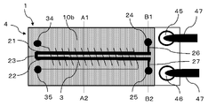
- FIG. 1 is a plan view of a GSR sensor and a GSR element in the embodiment and the example.
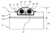
- FIG. 2 is a cross-sectional view taken along line A1-A2 of FIG.
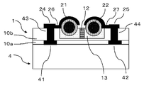
- FIG. 3 is a cross-sectional view taken along line B1-B2 of FIG.
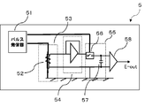
- FIG. 4 is a diagram of the electronic circuit in the embodiment and the example.
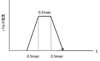
- FIG. 5 is a diagram showing the relationship between the passage of the conduction time and the application of the pulse current when the pulse current is supplied to the element.
- the ultra-compact high-sensitivity magnetic sensor according to the present invention comprises an insulating protective film formed on an ASIC and a wiring plane of the ASIC, a substrate film formed on the protective film, and a magnetic field detection element formed on the substrate film
- the magnetic field detection element is composed of a magnetic wire and a detection coil and electrodes that circulate around the magnetic wire on the substrate film.
- the magnetic wire has a two-phase magnetic domain structure of a surface magnetic domain having conductivity and an anisotropic magnetic field of 20 G or less and having a circumferential spin alignment and a central core magnetic domain having an axial spin alignment.
- the detection coil has a coil pitch of 10 ⁇ m or less.
- the electrode penetrates the substrate film and the insulating protective film, and is directly bonded to the element connection electrode of the ASIC in a through hole manner.
- a film having a thickness capable of serving as a substrate of the magnetic field detection element is formed on the insulating protective film on the surface of the ASIC, and the film is used as the substrate.
- a groove is attached to the substrate film, and a magnetic wire is aligned with the groove to produce a magnetic field detection element. That is, the sensor formed of the magnetic field detection element integrally formed with the ASIC can be thinned, and can be miniaturized.
- the ASIC of the ultra-compact high-sensitivity magnetic sensor of the present invention is generated when a pulse current of a converted frequency of 0.2 GHz to 4.0 GHz is caused to flow through the magnetic wire of the magnetic field detection element and a pulse current flows through the magnetic wire. It comprises means for detecting the coil voltage and means for converting the coil voltage into an electrical signal proportional to the external magnetic field H. Note that high sensitivity can be realized by supplying a pulse current of 0.2 to 4.0 GHz.
- the thickness of the substrate film of the ultra-compact high-sensitivity magnetic sensor of the present invention is 1 ⁇ m to 20 ⁇ m.
- the substrate coating needs to be thick enough to be grooved to receive the magnetic wire.
- the diameter of the magnetic wire assumed is 1 ⁇ m to 10 ⁇ m.
- the thickness of the substrate film is preferably 1 ⁇ m to 20 ⁇ m.
- a sufficient thickness to have a function as a substrate in the insulating protective film is secured, a single-layer structure in which the insulating protective film doubles as the substrate film is also possible.
- the magnetic field detection element has a groove 1 ⁇ m to 10 ⁇ m deep from the top surface of the substrate film, and a part or all of the detection coil is embedded. According to the present invention, the magnetic field detection element can be miniaturized.
- FIG. 1 a plan view of a GSR sensor and a GSR sensor element (hereinafter referred to as an element) is shown in FIG. 1, a sectional view taken along line A1-A2 of the plan view is shown in FIG. 2, and a sectional view taken along line B1-B2. 3 show an embodiment of the present invention in detail.
- the magnetic wire consists of two, and the form which consists of 2 layers of an insulation protective film and a board
- the ultra-compact high-sensitivity magnetic sensor (hereinafter referred to as a sensor) of the present invention comprises a GSR sensor element 1 (hereinafter referred to as an element) and ASIC 4 and electrodes for external wiring (45 and 46) from the ASIC 4.
- the element 1 constituting the sensor includes two magnetic wires 2 (21 and 22) and one coil 3 around the magnetic wires on a substrate film 10b formed on the insulating protective film 10a of the ASIC 4 and Two electrodes (24 and 25) for wire conduction, two electrodes (34 and 35) for coil voltage detection, and connections (26 and 27) between magnetic wire and wire conduction electrode, coil and coil detection Connection part with electrode, through-hole type joint between coil electrode on the element side and coil electrode on ASIC side, through-hole type joint between wire electrode on the element side and wire electrode on ASIC side (43 and 44) It consists of Further, the element 2 includes a wire connecting portion 23 as means for supplying pulse current in the reverse direction to two magnetic wires.
- two coil electrodes and two wire electrodes are connected to the element 1 by the through-hole electrode junctions respectively, and a coil is generated in the detection coil when a pulse current is supplied to the element It comprises an electronic circuit that senses the voltage and converts the coil voltage into an external magnetic field.
- external wiring electrodes 45 and 46 are disposed in the ASIC.
- the external magnetic field H and the coil voltage Vs are represented by a mathematical relationship such as the following equation (1), and are converted into the external magnetic field H using this relationship.
- Vs V 0 ⁇ 2L ⁇ ⁇ D ⁇ p ⁇ Nc ⁇ f ⁇ sin ( ⁇ H / 2Hm) (1)
- Vs coil output voltage
- V 0 proportional constant
- L length of wire
- D diameter of wire
- p skin depth of pulse current
- Nc number of turns of coil
- f pulse frequency
- Hm Is the external magnetic field strength when the coil output voltage takes a maximum value.
- the structure of the device 1 is as shown in FIGS.
- the size of the element 1 is the size of the substrate 10, which is 0.07 mm to 0.4 mm wide and 0.25 mm to 1 mm long.
- the thickness is 10 ⁇ m to 15 ⁇ m. Therefore, since the thickness of the ASIC 4 is 30 ⁇ m to 100 ⁇ m, the thickness of the sensor is 40 ⁇ m to 115 ⁇ m.
- a groove 11 with a width of 20 ⁇ m to 60 ⁇ m and a depth of 1 ⁇ m to 10 ⁇ m is formed in the substrate film 10b so that two magnetic wires (21 and 22) can be aligned in parallel.
- the two magnetic wires (21 and 22) are close, and the distance between the two magnetic wires is 1 ⁇ m to 10 ⁇ m.
- the magnetic wire 21 and the magnetic wire 22 are separated by an insulating material, and for example, separation by the insulating separation wall 12 is preferable.
- the magnetic wire 2 has a diameter of 1 ⁇ m to 10 ⁇ m of a CoFeSiB alloy.
- the periphery of the magnetic wire 2 is preferably coated with an insulating material, for example, an insulating glass material.
- the length is 0.07 mm to 1 mm.
- the anisotropic magnetic field of the magnetic wire 2 is 20 G or less, and has a two-phase magnetic domain structure of a surface magnetic domain having a circumferential spin alignment and a central core magnetic domain having an axial spin alignment.
- the coil 3 has 6 to 180 turns and a coil pitch of 0.2 to 10 ⁇ m.
- the distance between the coil 3 and the magnetic wire 2 is 0.2 ⁇ m to 3 ⁇ m.
- the average coil inner diameter is 2 ⁇ m to 35 ⁇ m.
- a substrate film 10b is formed on the insulating protective film 10a on the surface of the ASIC, a groove with a depth of 1 ⁇ m to 10 ⁇ m is attached to the substrate film 10b, and the element is embedded to embed part to all of the coil along the groove surface.
- the thickness of the element portion 1 can be 20 ⁇ m or less from the surface of the ASIC. Further, by setting the thickness of the ASIC to about 30 ⁇ m, the thickness of the entire sensor can be set to about 50 ⁇ m.
- the substrate film 10 b can be formed on the insulating protective film 10 a on the top surface of the ASIC to form the device 1.
- a two-layered film of an insulating protective film and a substrate film is formed, it is possible to use a single-layered film as long as the insulating protective film has a sufficient thickness to have a function as a substrate.
- a SiO 2 (silicon dioxide) film is formed with a thickness of 0.5 ⁇ m to 2 ⁇ m on an ASIC surface by vacuum evaporation or the like, and a SiN (silicon nitride) film is further formed on the upper surface of the film It is formed with a thickness of ⁇ 10 ⁇ m.
- a groove with a depth of 1 ⁇ m to 10 ⁇ m is attached to the SiN film, and an element is formed so as to embed part or all of the coil along the groove surface.
- Electrode wiring is performed on the lower coil 31 and the substrate film surface along the groove 11 formed in the substrate film 10b. Thereafter, an insulating separation wall 12 is formed at the central portion of the groove 11 to form two groove shapes, and two glass-coated magnetic wires (21 and 22) are respectively aligned and arranged there. Next, an insulating resist is applied to the entire surface of the substrate film. Thus, the magnetic wires (21 and 22) are fixed in the groove 11. The top of the magnetic wires (21 and 22) is thinly applied during this application.
- the upper coil 32 is formed there by photolithography.
- the material of the substrate film is not limited to oxide and nitride as long as the characteristics required here are satisfied.
- an insulating material is apply
- the concave lower coil 31 is formed along the groove surface of the groove 11 formed in the substrate film 10 b and both sides of the groove 11.
- the convex upper coil 32 is electrically connected to the lower coil 31 through the joint portion 33 to form a spiral coil 3.
- the glass of the insulating coating material is removed to allow electrical connection by metal deposition.
- the wire input electrode (+) 24 is connected to the upper magnetic wire 21 and is connected to the lower magnetic wire 22 via the wire connection portion 23.
- the lower magnetic wire 22 is connected to the wire output electrode ( ⁇ ) 25. Due to this wire connection portion, a leftward pulse current flows from the right to the left in the magnetic wire 21 and a rightward pulse (reverse to the magnetic wire 21) from the left to the right in the magnetic wire 22. The current can flow.
- the coil output electrode (+) 34 is connected to the upper end of the coil 3
- the coil ground electrode ( ⁇ ) is connected to the lower end of the coil 3.
- the electrode on the element side and the electrode on the ASIC side are electrically connected via a through hole type joint (43 and 44) penetrating the insulating protective film 10a and the substrate film 10b as shown in the example of FIG. Ru.
- the magnetic wire input electrode (+) 24 on the element side is a wire electrode (+) 41 on the ASIC side through the through-hole type electrode joint portion (+) 43 penetrating the insulating protective film 10a and the substrate film 10b.
- the magnetic wire output electrode (-) 25 on the element side is connected to the wire electrode (-) on the ASIC side via the through-hole type electrode joint (-) 44 that penetrates the insulating protective film 10a and the substrate film 10b. It shows that it is connected to 42.
- the coil electrode on the element side and the coil electrode on the ASIC side are connected via an electrode joint portion penetrating the insulating protective film 10 a and the substrate film 10 b.
- the electronic circuit 5 is shown in FIG. 4 with reference to the pulse corresponding buffer circuit described in Patent Document 1.
- the electronic circuit 5 is connected to an element 52 for outputting a coil voltage, and a pulse oscillation circuit 51 for transmitting a pulse current to the element 52, an input circuit 53 for inputting a coil voltage, a pulse corresponding buffer circuit 54, a coil
- the sample and hold circuit 55 including an electronic switch 56 for detecting the peak voltage of the rising pulse output waveform and the capacitor 57 having a capacitance of 4 pF to 100 pF for holding the peak voltage and amplification by the programming amplifier of the amplifier 58 performs AD conversion. Transfer the signal to an external signal processor with two wires.
- AD conversion is 14 bits to 16 bits.
- the capacitance is preferably 4 pF to 8 pF.
- the conversion frequency of the pulse current is 0.2 GHz to 4 GHz
- the intensity of the pulse current is 50 mA to 200 mA
- the pulse conduction time is 2 nsec or less.
- FIG. 5 shows the relationship between the passage of the conduction time and the application of the pulse current when the pulse current is supplied to the element. In the example of FIG. 5, it rises at 0.5 nsec, holds a predetermined pulse time of 0.5 nsec in its applied state, and falls at 0.5 nsec.
- the coil output is a sine wave output with a measurement range of 3 G to 100 G, and its sensitivity is 50 mV / G to 3 V / G.
- the linearity of the coil output is 0.3% or less.
- FIG. 1 is a plan view of the GSR sensor and the GSR sensor element according to the embodiment
- FIG. 2 is a cross-sectional view taken along line A1-A2 of the plan view
- FIG. 3 is a cross-sectional view taken along line B1-B2.
- the size of the element 1 is 0.10 mm in width and 0.40 mm in length.
- the thickness 40 of the ASIC 4 is 50 ⁇ m
- the thickness 14 of the insulating protective film 10 a and the substrate film 10 b is 8 ⁇ m
- the thickness of the convex portion of the element is 2 ⁇ m
- the thickness of the sensor combining these is 60 ⁇ m.
- a groove 11 having a width of 20 ⁇ m and a depth of 3 ⁇ m is formed in the substrate film 10b so that two magnetic wires (21 and 22) can be aligned in parallel.
- the two magnetic wires (21 and 22) are in close proximity, and the distance between the magnetic wires is 3 ⁇ m, and the magnetic wires (21 and 22) are separated by the insulating separation wall 12 with a thickness of 3 ⁇ m.
- the magnetic wire 2 is 5 ⁇ m in diameter of the CoFeSiB amorphous alloy.
- the periphery of the magnetic wire 2 is covered with an insulating glass.
- the length is 0.40 mm.
- the anisotropic magnetic field of the magnetic wire 2 is 15 G, and has a two-phase magnetic domain structure of a surface magnetic domain having a circumferential spin alignment and a central core magnetic domain having an axial spin alignment.
- the coil 3 has 100 turns and a coil pitch of 3 ⁇ m.
- the distance between the coil 3 and the magnetic wire 2 is 2 ⁇ m, and the average coil inner diameter is 8 ⁇ m
- a substrate film 10b having a thickness of 7 ⁇ m is formed on the insulating protective film 10a on the upper surface of the ASIC, and a groove having a depth of 3 ⁇ m is attached thereto to fabricate an element 1.
- the capacitance of the capacitor 57 of the electronic circuit 5 is 6 pF.
- the conversion frequency of the pulse current is 0.4 GHz, the intensity of the pulse current is 50 mA, and the pulse time is 1 nsec.
- the timing of the peak voltage of the rising pulse is detected.
- the electronic switch is on-off, and its open / close time is repeated at 0.1 nsec.
- the AD conversion of the electronic circuit 5 is 16 bits.
- the coil output has a measurement range of 3 G and its sensitivity is 1000 mV / G.
- the linearity is 0.3% or less.
- the present invention integrates a device and an ASIC to realize ultra-miniaturization of a GSR sensor, and is expected to be used in applications requiring ultra-compact and high performance, such as in-vivo motion devices.
- the present invention is applicable to small-sized ultra-high sensitivity GSR sensors such as those for automobiles or wearable computers.
- GSR sensor element 10a insulating protective film a
- 10b substrate film b
- 11 groove
- 12 insulating separation wall
- 13 insulating resist
- 14 element thickness 2: magnetic wire 21: magnetic pair forming a pair One of the wires
- 22 The other one of the pair of magnetic wires
- 34 Coil output electrode (+), 35: Coil ground electrode (-) 4: ASIC 40: thickness of ASIC, 41: ASIC side wire electrode (+), 42: ASIC side wire electrode (-), 43: through hole type electrode joint (+), 44: through hole type electrode joint (-), 45: external wiring electrode 46: external wiring earth electrode 47: external wiring 5: electronic circuit 51: pulse transmission circuit (pulse transmitter) 52: element 53: input circuit 54: buffer circuit 55: Sample and
Landscapes
- Physics & Mathematics (AREA)
- Condensed Matter Physics & Semiconductors (AREA)
- General Physics & Mathematics (AREA)
- Engineering & Computer Science (AREA)
- Manufacturing & Machinery (AREA)
- Hall/Mr Elements (AREA)
- Measuring Magnetic Variables (AREA)
Abstract
ASICと一体形成した磁界検出素子からなる超小型高感度磁気センサを提供するため、本発明は、ASIC(4)の絶縁保護被膜(10a)上面に形成する基板皮膜(10b)の厚みを1μm~20μmとし、その基板皮膜上(10b)に深さ1μm~10μmの溝(11)を取り付け、その溝(11)面に沿ってコイルの一部又は全部を埋設するように素子(1)を形成し、素子(1)の電極とASIC(4)の電極とは絶縁保護被膜(10a)及び基板皮膜(10b)を貫通するスルーホール方式の電極接合部を介して電気接続し、ASIC(4)表面からの素子部の厚みを20μm以下とする。
Description
本発明は、GSR素子と特定用途向け集積回路(以下、ASICという。)との一体形成によりGSRセンサのサイズや厚みを超小型化する技術に関するものである。
ここで、GSRセンサとは超高速スピン回転効果(英語表記;GHz Spin Rotation effect)を基礎にした高感度マイクロ磁気センサである。
ここで、GSRセンサとは超高速スピン回転効果(英語表記;GHz Spin Rotation effect)を基礎にした高感度マイクロ磁気センサである。
高感度マイクロ磁気センサには、横型FGセンサ、縦型FGセンサ、ホールセンサ、GMRセンサ、TMRセンサ、MIセンサ、GSRセンサ、高周波キャリアセンサなどがある。現在、これらのセンサは、スマートフォン、自動車、医療、ロボットなどに広く採用されている。その中でもGSRセンサ(特許文献1)は、感度面とサイズ面において優れており、最も注目されている。
現在、カテーテルなどのような生体内モーションデバイスに磁気センサを搭載して位置や方位を求めて、その測定値を活用したリモートコントロール治療を実現するための研究(特許文献2、3)が進んでいる。
生体内モーションデバイスに搭載するためには、センササイズは小さいほど好ましいが、それに反比例して検出感度が低下するので、必要な検出感度を保ちながら小型化するのは難しい。例えばカテーテルに搭載する場合には、サイズ面では幅0.1mm、長さ0.3mm、厚み0.05mm程度の超小型サイズで、磁界検出力の面では0.1mGから1mG程度の優れた超高感度性能を兼ね合わせ持つ磁気センサの開発が期待されている。
生体内モーションデバイスに搭載するためには、センササイズは小さいほど好ましいが、それに反比例して検出感度が低下するので、必要な検出感度を保ちながら小型化するのは難しい。例えばカテーテルに搭載する場合には、サイズ面では幅0.1mm、長さ0.3mm、厚み0.05mm程度の超小型サイズで、磁界検出力の面では0.1mGから1mG程度の優れた超高感度性能を兼ね合わせ持つ磁気センサの開発が期待されている。
GSRセンサを小型化するために、GSR素子の小型化、ASICの小型化および両部品の接合方法(特許文献4)など多面的に取り組まれている。しかし、いずれの取り組みも素子とASICを別々に分けて2部品として製造してから、両者を接合しているために小型化、特に厚みの縮小という点で限界があった(特許文献4および5)。
本発明者は、ASICとGSR素子との接合について鋭意検討した結果、ASIC本体の絶縁保護被膜上に、GSR素子の基板となる皮膜を形成し、その基板皮膜上に磁性ワイヤを配列する溝を取り付け、磁性ワイヤとその磁性ワイヤを周回する検出コイルからなるGSR素子を一体形成することにより薄型化できることに想到した。
GSR素子の基板皮膜としては、SiO2、Al2O3などの酸化物およびSiNなどの窒化物が可能であることを見出した。
すなわち、これらの基板皮膜を用いた場合には、GSR素子をASIC表面上に直接形成する場合に、GSR素子の製造プロセスに含まれているマイクロ溝の加工、CF4ガスプラズマ処理、レジスト加熱キュア処理、酸やアルカリを使う現像処理などの工程があり、ASIC表面の絶縁保護被膜の損傷とその損傷によるGSR素子基板の下のASIC回路の機能性の低下などは認められなかった。
すなわち、これらの基板皮膜を用いた場合には、GSR素子をASIC表面上に直接形成する場合に、GSR素子の製造プロセスに含まれているマイクロ溝の加工、CF4ガスプラズマ処理、レジスト加熱キュア処理、酸やアルカリを使う現像処理などの工程があり、ASIC表面の絶縁保護被膜の損傷とその損傷によるGSR素子基板の下のASIC回路の機能性の低下などは認められなかった。
さらに、絶縁保護被膜を厚く形成して絶縁保護被膜上に素子を形成する、単層構造とすることも可能であることを見出した。
そして、ASICとGSR素子の接合に基板皮膜及び絶縁保護被膜を貫通するスルーホール式接合を採用することにより、電極のサイズを小さくすることでGSR素子全体の面積を小さくできることを想到した。
本発明によれば、GSRセンサの薄型化、超小型化が可能になる。
本発明の実施形態について、次の通りである。
本発明の超小型高感度磁気センサは、ASICとASICの配線平面上に形成された絶縁保護被膜と保護被膜上に形成された基板皮膜および基板皮膜上に形成される磁界検出素子とからなり、 磁界検出素子は、基板皮膜の上に磁性ワイヤと磁性ワイヤを周回する検出コイルと電極からなっている。
磁性ワイヤは、導電性と20G以下の異方性磁界を有し、かつ円周方向スピン配列を持つ表面磁区と軸方向にスピン配列を持つ中央部コア磁区の2相の磁区構造を有している。検出コイルは、コイルピッチ10μm以下である。
電極は、基板皮膜及び絶縁保護被膜を貫いてASICの素子連結用電極とスルーホール方式で直接接合する。
本発明の超小型高感度磁気センサは、ASICとASICの配線平面上に形成された絶縁保護被膜と保護被膜上に形成された基板皮膜および基板皮膜上に形成される磁界検出素子とからなり、 磁界検出素子は、基板皮膜の上に磁性ワイヤと磁性ワイヤを周回する検出コイルと電極からなっている。
磁性ワイヤは、導電性と20G以下の異方性磁界を有し、かつ円周方向スピン配列を持つ表面磁区と軸方向にスピン配列を持つ中央部コア磁区の2相の磁区構造を有している。検出コイルは、コイルピッチ10μm以下である。
電極は、基板皮膜及び絶縁保護被膜を貫いてASICの素子連結用電極とスルーホール方式で直接接合する。
本発明によれば、ASIC表面の絶縁保護被膜上に磁界検出素子の基板としての機能を果たすことができる厚みの皮膜を形成し、その皮膜を基板として用いる。基板皮膜に溝を取り付け、溝に磁性ワイヤを整列させて磁界検出素子を作製する。すなわち、ASICと一体形成した磁界検出素子からなるセンサは薄型化が可能となり、超小型を実現できる。
また、本発明の超小型高感度磁気センサのASICは、磁界検出素子の磁性ワイヤに0.2GHz~4.0GHzの換算周波数のパルス電流を流す手段と、磁性ワイヤにパルス電流を流した時に生じるコイル電圧を検知する手段と、コイル電圧を外部磁界Hに比例する電気信号に変換する手段を有する。なお、0.2~4.0GHzのパルス電流を流すことにより高感度化が実現される。
また、本発明の超小型高感度磁気センサの基板皮膜の厚みは、1μm~20μmからなる。
本発明によれば、基板皮膜は磁性ワイヤを収める溝を付けられるだけの厚みを必要とする。想定される磁性ワイヤの直径は1μm~10μmである。また、基板皮膜が厚すぎると絶縁保護被膜との密着性に問題が生ずる。従って、基板皮膜の厚みは1μm~20μmが望ましい。また絶縁保護被膜に基板としての機能を有するのに十分な厚さを確保すれば、絶縁保護被膜が基板皮膜を兼ねる単層構造も可能である。
本発明によれば、基板皮膜は磁性ワイヤを収める溝を付けられるだけの厚みを必要とする。想定される磁性ワイヤの直径は1μm~10μmである。また、基板皮膜が厚すぎると絶縁保護被膜との密着性に問題が生ずる。従って、基板皮膜の厚みは1μm~20μmが望ましい。また絶縁保護被膜に基板としての機能を有するのに十分な厚さを確保すれば、絶縁保護被膜が基板皮膜を兼ねる単層構造も可能である。
さらに、本発明の超小型高感度磁気センサは、磁界検出素子は基板皮膜上面から深さ1μm~10μmの溝を配置し、検出コイルの一部又は全部が埋設されている。
本発明によれば、磁界検出素子の小型化を図ることができる。
本発明によれば、磁界検出素子の小型化を図ることができる。
以下に、GSRセンサとGSRセンサ素子(以下、素子という。)の平面図を図1に示し、その平面図のA1-A2線の断面図を図2に、B1-B2線の断面図を図3に示して、本発明の実施形態について詳細に説明する。
本説明では、磁性ワイヤは2本からなり、絶縁保護被膜と基板皮膜の2層からなる形態について説明する。
本発明の超小型高感度磁気センサ(以下、センサという。)は、GSRセンサ素子1(以下、素子という。)とASIC4およびASIC4からの外部配線用電極(45および46)からなる。
本説明では、磁性ワイヤは2本からなり、絶縁保護被膜と基板皮膜の2層からなる形態について説明する。
本発明の超小型高感度磁気センサ(以下、センサという。)は、GSRセンサ素子1(以下、素子という。)とASIC4およびASIC4からの外部配線用電極(45および46)からなる。
<センサ>
センサを構成する素子1は、ASIC4の絶縁保護被膜10aの上に形成される基板皮膜10bの上に2本の磁性ワイヤ2(21および22)とその磁性ワイヤを周回する1個のコイル3およびワイヤ通電用の2個の電極(24および25)とコイル電圧検出用の2個の電極(34および35)ならびに磁性ワイヤとワイヤ通電用電極との接続部(26および27)、コイルとコイル検出電極との接続部および素子側のコイル電極とASIC側のコイル電極とのスルーホール方式の接合部、素子側のワイヤ電極とASIC側のワイヤ電極とのスルーホール方式の接合部(43および44)からなる。
また、素子2には磁性ワイヤ2本に逆向きのパルス電流を流す手段としてワイヤ連結部23からなる。
そして、ASIC4は、素子1との間は2個のコイル電極および2個のワイヤ電極がそれぞれスルーホール方式の電極接合部により接続されて、素子にパルス電流を流したときに検出コイルに生じるコイル電圧を検知し、コイル電圧を外部磁界に変換する電子回路からなる。また、ASICには外部配線用電極(45および46)が配置されている。
ここで、GSRセンサにおける検知したコイル電圧から外部磁界を求める方法について説明する。
外部磁界Hとコイル電圧Vsは、次式(1)のような数学的関係で表され、本関係式を使って外部磁界Hに変換するものである。
Vs=V0・2L・πD・p・Nc・f・sin(πH/2Hm) (1)
ここで、Vsはコイル出力電圧、V0は比例定数、Lはワイヤの長さ、Dはワイヤの直径、pはパルス電流の表皮深さ、Ncはコイルの巻き数、fはパルス周波数、Hmはコイル出力電圧が最大値を取る時の外部磁界強度である。
外部磁界Hとコイル電圧Vsは、次式(1)のような数学的関係で表され、本関係式を使って外部磁界Hに変換するものである。
Vs=V0・2L・πD・p・Nc・f・sin(πH/2Hm) (1)
ここで、Vsはコイル出力電圧、V0は比例定数、Lはワイヤの長さ、Dはワイヤの直径、pはパルス電流の表皮深さ、Ncはコイルの巻き数、fはパルス周波数、Hmはコイル出力電圧が最大値を取る時の外部磁界強度である。
<素子の構造>
素子1の構造は、図1~図3に示すとおりである。
素子1のサイズは、基板10のサイズである幅0.07mm~0.4mm、長さ0.25mm~1mmである。厚みは10μm~15μmである。よって、ASIC4の厚みが30μm~100μmであることからセンサの厚みは40μm~115μmとなる。
素子1の中央部には、磁性ワイヤ2本(21および22)が平行に整列配置できるように幅20μm~60μm、深さ1μm~10μmの溝11が基板皮膜10bに形成されている。2本の磁性ワイヤ(21および22)は近接しており、2本の磁性ワイヤの間隔は1μm~10μmである。そして、磁性ワイヤ21と磁性ワイヤ22とは絶縁材料で隔離されおり、例えば絶縁性分離壁12による隔離が好ましい。
<磁性ワイヤ>
磁性ワイヤ2は、CoFeSiB合金の直径1μm~10μmである。磁性ワイヤ2の周囲は絶縁性材料、例えば絶縁性ガラス材料で被覆されていることが好ましい。長さは0.07mm~1mmである。
磁性ワイヤ2の異方性磁界は20G以下で、円周方向スピン配列を持つ表面磁区と軸方向にスピン配列を持つ中央部コア磁区の2相の磁区構造を有する。
磁性ワイヤ2は、CoFeSiB合金の直径1μm~10μmである。磁性ワイヤ2の周囲は絶縁性材料、例えば絶縁性ガラス材料で被覆されていることが好ましい。長さは0.07mm~1mmである。
磁性ワイヤ2の異方性磁界は20G以下で、円周方向スピン配列を持つ表面磁区と軸方向にスピン配列を持つ中央部コア磁区の2相の磁区構造を有する。
<コイル>
コイル3は、コイル巻き数は6回~180回、コイルピッチは0.2μm~10μmである。コイル3と磁性ワイヤ2との間隔は0.2μm~3μmである。コイル平均内径は2μm~35μmである。
コイル3は、コイル巻き数は6回~180回、コイルピッチは0.2μm~10μmである。コイル3と磁性ワイヤ2との間隔は0.2μm~3μmである。コイル平均内径は2μm~35μmである。
<素子の製造方法>
ASICの表面の絶縁保護被膜10a上に基板皮膜10bを形成し、その基板皮膜10bに深さ1μm~10μmの溝を取り付け、溝面に沿ってコイルの一部~全部を埋設するように素子を形成することによってASIC表面から素子部1の厚みを20μm以下にすることができる。さらにASICの厚みを30μm程度とすることによりセンサ全体の厚みを50μm程度とすることができる。
ASICの表面の絶縁保護被膜10a上に基板皮膜10bを形成し、その基板皮膜10bに深さ1μm~10μmの溝を取り付け、溝面に沿ってコイルの一部~全部を埋設するように素子を形成することによってASIC表面から素子部1の厚みを20μm以下にすることができる。さらにASICの厚みを30μm程度とすることによりセンサ全体の厚みを50μm程度とすることができる。
ASIC上面の絶縁保護被膜10aの上に基板皮膜10bを形成して素子1を形成できる。絶縁保護被膜と基板皮膜の2層の膜を形成するが、絶縁保護被膜に基板としての機能を有するのに十分な厚さを確保すれば1層の膜でも可能である。2層の膜の例として、SiO2(二酸化珪素)膜を0.5μm~2μmの厚みでASIC表面上に真空蒸着法などにより形成し、その膜の上面にさらにSiN(窒化珪素)膜を1μm~10μmの厚みで形成する。SiN膜に深さ1μm~10μmの溝を取り付け、溝面に沿ってコイルの一部あるいは全部を埋設するように素子を形成する。
基板皮膜10bに形成されている溝11に沿って下コイル31と基板皮膜面上に電極配線を行う。その後、溝11の中央部に絶縁性分離壁12を形成して2つの溝形状とし、そこに2本のガラス被覆した磁性ワイヤ(21および22)をそれぞれ整列配置する。
次いで、基板皮膜全面に絶縁性レジストを塗布する。こうして磁性ワイヤ(21および22)は溝11内に固定される。この塗布の際に磁性ワイヤ(21および22)の上部は薄く塗布する。そこに上コイル32をフォトリソ技術で形成する。
次いで、基板皮膜全面に絶縁性レジストを塗布する。こうして磁性ワイヤ(21および22)は溝11内に固定される。この塗布の際に磁性ワイヤ(21および22)の上部は薄く塗布する。そこに上コイル32をフォトリソ技術で形成する。
ここで、基板皮膜および絶縁保護被膜の特性として、素子1の製造プロセスにおけるマイクロ溝加工、CF4ガスプラズマ処理、レジスト加熱キュア処理、酸やアルカリを使う現像処理などの工程における耐性とASIC回路の機能性低下の防止が求められる。従って、ここで求められる特性を満たせば、基板皮膜の材質は酸化物及び窒化物に限るものではない。
なお、ガラス被覆していない磁性ワイヤ2を用いる場合には、下コイル31と磁性ワイヤ(21および22)とが電気的な接触が生じないように予め絶縁性材料を塗布する。
なお、ガラス被覆していない磁性ワイヤ2を用いる場合には、下コイル31と磁性ワイヤ(21および22)とが電気的な接触が生じないように予め絶縁性材料を塗布する。
コイルの作製は、基板皮膜10bに形成された溝11の溝面および溝11の両側に沿って凹形状の下コイル31が形成される。凸形状の上コイル32はジョイント部33を介して下コイル31と電気的接合がされ、らせん状のコイル3となる。
2本の磁性ワイヤ(21および22)の端部については、絶縁性被膜材のガラスを除去して金属蒸着による電気的接続をできるようにする。
<磁性ワイヤとコイルの配線構造>
磁性ワイヤ2とコイル3の配線構造について、図1を用いて説明する。
磁性ワイヤ2の配線構造は、ワイヤ入力電極(+)24は上部の磁性ワイヤ21と接続され、ワイヤ連結部23を介して下部の磁性ワイヤ22に接続されている。下部の磁性ワイヤ22はワイヤ出力電極(-)25に接続されている。
このワイヤ連結部により、磁性ワイヤ21では右部から左部への左向きのパルス電流が流れ、磁性ワイヤ22では左部から右部への右向き(磁性ワイヤ21とは逆向きになる。)のパルス電流を流すことができる。
磁性ワイヤ2とコイル3の配線構造について、図1を用いて説明する。
磁性ワイヤ2の配線構造は、ワイヤ入力電極(+)24は上部の磁性ワイヤ21と接続され、ワイヤ連結部23を介して下部の磁性ワイヤ22に接続されている。下部の磁性ワイヤ22はワイヤ出力電極(-)25に接続されている。
このワイヤ連結部により、磁性ワイヤ21では右部から左部への左向きのパルス電流が流れ、磁性ワイヤ22では左部から右部への右向き(磁性ワイヤ21とは逆向きになる。)のパルス電流を流すことができる。
コイル3の配線構造は、コイル出力電極(+)34はコイル3の上端部と接続され、コイルグランド電極(-)はコイル3の下端部と接続されている。
素子側の電極とASIC側の電極とは、図3の例に示すように絶縁保護被膜10aおよび基板皮膜10bを貫通するスルーホール方式の接合部(43および44)を介して電気的に接続される。
図3は、素子側の磁性ワイヤ入力電極(+)24は絶縁保護被膜10aおよび基板皮膜10bを貫通するスルーホール方式の電極接合部(+)43を介してASIC側のワイヤ電極(+)41と接続され、素子側の磁性ワイヤ出力電極(-)25は絶縁性保護被膜10aおよび基板皮膜10bを貫通するスルーホール方式の電極接合部(-)44を介してASIC側のワイヤ電極(-)42に接続されていること示している。
同様に、素子側のコイル電極とASIC側のコイル電極とは絶縁保護被膜10aおよび基板皮膜10bを貫通する電極接合部を介して接続されている。
図3は、素子側の磁性ワイヤ入力電極(+)24は絶縁保護被膜10aおよび基板皮膜10bを貫通するスルーホール方式の電極接合部(+)43を介してASIC側のワイヤ電極(+)41と接続され、素子側の磁性ワイヤ出力電極(-)25は絶縁性保護被膜10aおよび基板皮膜10bを貫通するスルーホール方式の電極接合部(-)44を介してASIC側のワイヤ電極(-)42に接続されていること示している。
同様に、素子側のコイル電極とASIC側のコイル電極とは絶縁保護被膜10aおよび基板皮膜10bを貫通する電極接合部を介して接続されている。
<電子回路>
電子回路5は、特許文献1に記載のパルス対応型バッファー回路を参照し、図4に示す。
電子回路5は、コイル電圧を出力する素子52が接続されており、その素子52にパルス電流を発信するパルス発振回路51、コイル電圧を入力する入力回路53、パルス対応型バッファー回路54、コイルの立ち上がりパルス出力波形のピーク電圧を検波する電子スイッチ56とピーク電圧を保持する容量4pF~100pFのコンデンサ57からなるサンプルホールド回路55、および増幅器58のプログラミングアンプにて増幅してAD変換を行なう。2本のワイヤにて信号を外部の信号処理装置に転送する。
電子回路5は、特許文献1に記載のパルス対応型バッファー回路を参照し、図4に示す。
電子回路5は、コイル電圧を出力する素子52が接続されており、その素子52にパルス電流を発信するパルス発振回路51、コイル電圧を入力する入力回路53、パルス対応型バッファー回路54、コイルの立ち上がりパルス出力波形のピーク電圧を検波する電子スイッチ56とピーク電圧を保持する容量4pF~100pFのコンデンサ57からなるサンプルホールド回路55、および増幅器58のプログラミングアンプにて増幅してAD変換を行なう。2本のワイヤにて信号を外部の信号処理装置に転送する。
AD変換は14ビット~16ビットである。電子スイッチのon-offを細かくするためにはコンデンサ容量は4pF~8pFが好ましい。
パルス電流の換算周波数は0.2GHz~4GHzにて、パルス電流の強度は50mA~200mA、パルス通電時間は2nsec以下である。図5には、素子にパルス電流を通電した時の通電時間の経過とパルス電流の印可との関係を表している。この図5の例では、0.5nsecで立ち上がり、その印可状態で所定のパルス時間0.5nsecを保持し、0.5nsecで立ち下がる。
コイル出力は正弦波出力にて測定レンジ3G~100Gで、その感度は50mV/G~3V/Gである。そのコイル出力の直線性は0.3%以下である。
実施例に係るGSRセンサとGSRセンサ素子の平面図を図1に示し、その平面図のA1-A2線の断面図を図2に、B1-B2線の断面図を図3に示して、本発明の実施例について説明する。
ここで、GSRセンサの構成および素子の構成、電子回路は上述の実施形態による。
ここで、GSRセンサの構成および素子の構成、電子回路は上述の実施形態による。
素子1のサイズは、幅0.10mm、長さ0.40mmからなる。厚みはASIC4の厚み40が50μm、絶縁保護被膜10aおよび基板皮膜10bの厚み14が8μmで、素子の凸部の厚みが2μm、これらを合計したセンサの厚みは60μmである。
素子1の中央部は、磁性ワイヤ2本(21および22)が平行に整列配置できるように幅20μm、深さ3μmの溝11が基板皮膜10bに形成されている。2本の磁性ワイヤ(21および22)は近接しており磁性ワイヤの間隔は3μmであり、磁性ワイヤ(21および22)同士は厚さ3μmの絶縁性分離壁12で隔離されている。
素子1の中央部は、磁性ワイヤ2本(21および22)が平行に整列配置できるように幅20μm、深さ3μmの溝11が基板皮膜10bに形成されている。2本の磁性ワイヤ(21および22)は近接しており磁性ワイヤの間隔は3μmであり、磁性ワイヤ(21および22)同士は厚さ3μmの絶縁性分離壁12で隔離されている。
磁性ワイヤ2は、CoFeSiBアモルファス合金の直径5μmである。磁性ワイヤ2の周囲は絶縁性ガラスで被覆されている。長さは0.40mmである。
磁性ワイヤ2の異方性磁界は15Gで、円周方向スピン配列を持つ表面磁区と軸方向にスピン配列を持つ中央部コア磁区の2相の磁区構造を有している。
磁性ワイヤ2の異方性磁界は15Gで、円周方向スピン配列を持つ表面磁区と軸方向にスピン配列を持つ中央部コア磁区の2相の磁区構造を有している。
コイル3は、コイル巻き数は100回、コイルピッチは3μmである。コイル3と磁性ワイヤ2との間隔は2μmで、コイル平均内径は8μmである
ASIC上面の絶縁保護被膜10aに厚み7μmの基板皮膜10bを形成し、そこに深さ3μmの溝を取り付け、素子1を作製する。
電子回路5のコンデンサ57の静電容量は6pFである。パルス電流の換算周波数は0.4GHzにて、パルス電流の強度は50mA、パルス時間は1nsecである。立ち上がりパルスのピーク電圧のタイミングを検波する。電子スイッチはon-offからなりその開閉時間は0.1nsecで繰り返す。電子回路5のAD変換は16ビットである。
コイル出力は、測定レンジ3Gで、その感度は1000mV/Gである。直線性は0.3%以下である。
本発明は、素子とASICとを一体化してGSRセンサの超小型化を実現するもので、生体内のモーションデバイスのように超小型で高性能を要求される用途での使用が期待される。
本発明は、自動車用あるいはウェアラブルコンピュータ用などの小型・超高感度GSRセンサに応用可能である。
1:GSRセンサ素子
10a:絶縁保護被膜a、10b:基板皮膜b、11:溝、12:絶縁性分離壁、13:絶縁性レジスト、14:素子の厚み
2:磁性ワイヤ
21:対をなす磁性ワイヤの一つ、22:対をなす磁性ワイヤの他の一つ、23:ワイヤ連結部、24:ワイヤ入力電極(+)、25:ワイヤ出力電極(-)、26:ワイヤ―電極接続部(+)、27:ワイヤ―電極接続部(-)
3:コイル
31:下コイル、32:上コイル、33:ジョイント部、34:コイル出力電極(+)、35:コイルグランド電極(-)
4:ASIC
40:ASICの厚み、41:ASIC側ワイヤ電極(+)、42:ASIC側ワイヤ電極(-)、43:スルーホール方式電極接合部(+)、44:スルーホール方式電極接合部(-)、45:外部配線用電極、46:外部配線用アース電極、47:外部配線
5:電子回路
51:パルス発信回路(パルス発信器)、52:素子、53:入力回路、54:バッファー回路、55:サンプルホールド回路、56:電子スイッチ、57:コンデンサ、58:増幅器
Claims (4)
- 特定用途向け集積回路(以下、ASICという。)と前記ASICの配線平面上に形成された絶縁保護被膜と前記保護被膜上に形成された基板皮膜および前記基板皮膜上に形成される磁界検出素子とからなる超小型高感度磁気センサにおいて、
前記磁界検出素子は、前記基板皮膜の上に磁性ワイヤと前記磁性ワイヤを周回する検出コイルと電極とを備えており、
前記磁性ワイヤは、導電性と20G以下の異方性磁界を有し、かつ円周方向スピン配列を持つ表面磁区と軸方向にスピン配列を持つ中央部コア磁区の2相の磁区構造を有しており、
前記検出コイルは、コイルピッチ10μm以下で、
前記電極は、前記基板皮膜及び前記絶縁保護被膜を貫いて前記ASICの素子連結用電極と直接接合することを特徴とする超小型高感度磁気センサ。 - 請求項1に記載されている超小型高感度磁気センサにおいて、
前記ASICは、前記磁界検出素子の磁性ワイヤに0.2GHz~4.0GHzの換算周波数のパルス電流を流す手段と前記磁性ワイヤにパルス電流を流した時に前記検出コイルに生じるコイル電圧を検知する手段と前記コイル電圧を外部磁界Hに比例する電気信号に変換する手段を有することを特徴とする超小型高感度磁気センサ。 - 請求項1に記載されている超小型高感度磁気センサにおいて、
前記基板皮膜は、厚み1μm~20μmを有することを特徴とする超小型高感度磁気センサ。 - 請求項1乃至請求項3のいずれか1項に記載されている超小型高感度磁気センサにおいて、
前記磁界検出素子は、前記基板皮膜上面から深さ1μm~10μmの溝を配置し、前記検出コイルの一部又は全部が埋設されていることを特徴とする超小型高感度磁気センサ。
Priority Applications (3)
| Application Number | Priority Date | Filing Date | Title |
|---|---|---|---|
| EP18834783.5A EP3657192B1 (en) | 2017-07-21 | 2018-05-22 | Ultra-small high-sensitivity magnetic sensor |
| CN201880039654.1A CN110753850B8 (zh) | 2017-07-21 | 2018-05-22 | 超小型高灵敏磁传感器 |
| US16/720,016 US11262419B2 (en) | 2017-07-21 | 2019-12-19 | Ultra-small and high-sensitivity magnetic sensor |
Applications Claiming Priority (2)
| Application Number | Priority Date | Filing Date | Title |
|---|---|---|---|
| JP2017141410A JP7262886B2 (ja) | 2017-07-21 | 2017-07-21 | 超小型高感度磁気センサ |
| JP2017-141410 | 2017-07-21 |
Related Child Applications (1)
| Application Number | Title | Priority Date | Filing Date |
|---|---|---|---|
| US16/720,016 Continuation US11262419B2 (en) | 2017-07-21 | 2019-12-19 | Ultra-small and high-sensitivity magnetic sensor |
Publications (1)
| Publication Number | Publication Date |
|---|---|
| WO2019017066A1 true WO2019017066A1 (ja) | 2019-01-24 |
Family
ID=65015185
Family Applications (1)
| Application Number | Title | Priority Date | Filing Date |
|---|---|---|---|
| PCT/JP2018/019705 WO2019017066A1 (ja) | 2017-07-21 | 2018-05-22 | 超小型高感度磁気センサ |
Country Status (5)
| Country | Link |
|---|---|
| US (1) | US11262419B2 (ja) |
| EP (1) | EP3657192B1 (ja) |
| JP (1) | JP7262886B2 (ja) |
| CN (1) | CN110753850B8 (ja) |
| WO (1) | WO2019017066A1 (ja) |
Cited By (1)
| Publication number | Priority date | Publication date | Assignee | Title |
|---|---|---|---|---|
| WO2024085097A1 (ja) * | 2022-10-17 | 2024-04-25 | マグネデザイン株式会社 | 磁界検出素子の製造方法 |
Families Citing this family (4)
| Publication number | Priority date | Publication date | Assignee | Title |
|---|---|---|---|---|
| JP6839399B1 (ja) * | 2020-09-29 | 2021-03-10 | マグネデザイン株式会社 | 磁界検出素子 |
| JP7329782B1 (ja) | 2022-12-09 | 2023-08-21 | マグネデザイン株式会社 | Gsr素子の製造方法 |
| EP4394417A1 (en) * | 2022-12-31 | 2024-07-03 | Melexis Technologies SA | Sensor device with circuit and integrated component for magneto-impedance measurement, and method of producing same |
| EP4394418A1 (en) * | 2022-12-31 | 2024-07-03 | Melexis Technologies SA | Semiconductor device with integrated soft-magnetic component, and method of producing same |
Citations (14)
| Publication number | Priority date | Publication date | Assignee | Title |
|---|---|---|---|---|
| JPS583975A (ja) | 1981-06-29 | 1983-01-10 | Hitachi Ltd | スパツタリングによる成膜方法及びその装置 |
| JPH03156391A (ja) * | 1989-11-14 | 1991-07-04 | Tdk Corp | 磁気検出装置 |
| JP2003167037A (ja) * | 2001-11-30 | 2003-06-13 | Tama Electric Co Ltd | 磁気センサ |
| JP2005147998A (ja) * | 2003-11-19 | 2005-06-09 | Fuji Electric Holdings Co Ltd | 磁気インピーダンスセンサ |
| US20060202291A1 (en) * | 2005-02-23 | 2006-09-14 | Stefan Kolb | Magnetoresistive sensor module and method for manufacturing the same |
| JP2009503443A (ja) * | 2005-07-22 | 2009-01-29 | リエゾン、エレクトロニク−メカニク、エルウエム、ソシエテ、アノニム | 直交フラックスゲート式磁界センサー |
| JP2014042055A (ja) | 2013-10-18 | 2014-03-06 | Nikon Corp | 基板重ね合わせ装置、基板保持装置および半導体装置の製造方法 |
| JP2014153309A (ja) | 2013-02-13 | 2014-08-25 | Magne Design Corp | 磁界検出素子 |
| EP2813859A1 (en) * | 2013-06-12 | 2014-12-17 | Nxp B.V. | Manufacturing magnetic sensor elements monolithically integrated at a semiconductor chip comprising an integrated circuit |
| JP2015134166A (ja) | 2014-01-17 | 2015-07-27 | バイオセンス・ウエブスター・(イスラエル)・リミテッドBiosense Webster (Israel), Ltd. | カテーテル編組ワイヤを使用する信号伝送 |
| JP5839527B1 (ja) * | 2015-02-16 | 2016-01-06 | マグネデザイン株式会社 | 超高感度マイクロ磁気センサ |
| JP2017012840A (ja) | 2011-11-22 | 2017-01-19 | アセンション テクノロジー コーポレイションAscension Technology Corporation | 追跡ガイドワイヤ |
| US9577185B1 (en) * | 2016-04-28 | 2017-02-21 | Texas Instruments Incorporated | Fluxgate device with low fluxgate noise |
| JP6256962B1 (ja) * | 2017-06-21 | 2018-01-10 | 朝日インテック株式会社 | 磁気式の方位・位置測定装置 |
Family Cites Families (14)
| Publication number | Priority date | Publication date | Assignee | Title |
|---|---|---|---|---|
| JP4007464B2 (ja) | 1997-10-06 | 2007-11-14 | Tdk株式会社 | 磁気探知装置 |
| JP2001296127A (ja) * | 2000-04-13 | 2001-10-26 | Aichi Steel Works Ltd | 磁場検出装置 |
| EP1336858A3 (en) * | 2002-02-19 | 2005-03-23 | Aichi Micro Intelligent Corporation | Two-dimensional magnetic sensor |
| JP4529783B2 (ja) * | 2005-04-25 | 2010-08-25 | 愛知製鋼株式会社 | マグネト・インピーダンス・センサ素子 |
| CN101410723B (zh) * | 2006-03-31 | 2011-09-14 | 西铁城电子股份有限公司 | 磁传感器元件和使用该元件的磁传感器 |
| CN101952961B (zh) * | 2008-02-25 | 2013-01-30 | 飞兆半导体公司 | 包括集成薄膜电感器的微模块及其制造方法 |
| JP4626728B2 (ja) * | 2009-03-26 | 2011-02-09 | 愛知製鋼株式会社 | 磁気検出装置 |
| CN102426344B (zh) * | 2011-08-30 | 2013-08-21 | 江苏多维科技有限公司 | 三轴磁场传感器 |
| JP6472140B2 (ja) | 2013-10-22 | 2019-02-20 | 国立大学法人九州大学 | 勾配磁界センサ |
| TWI538096B (zh) * | 2013-12-31 | 2016-06-11 | 財團法人工業技術研究院 | 具pn界面的微機電裝置 |
| JP6766333B2 (ja) | 2015-10-06 | 2020-10-14 | 愛知製鋼株式会社 | 微小磁性体検知センサおよび異物検知装置 |
| JP6864413B2 (ja) * | 2017-06-05 | 2021-04-28 | 朝日インテック株式会社 | Gsrセンサ素子 |
| JP7262885B2 (ja) * | 2017-06-16 | 2023-04-24 | 朝日インテック株式会社 | 超高感度マイクロ磁気センサ |
| EP3467528B1 (en) * | 2017-10-06 | 2020-05-20 | Melexis Technologies NV | Magnetic sensor sensitivity matching calibration |
-
2017
- 2017-07-21 JP JP2017141410A patent/JP7262886B2/ja active Active
-
2018
- 2018-05-22 EP EP18834783.5A patent/EP3657192B1/en active Active
- 2018-05-22 CN CN201880039654.1A patent/CN110753850B8/zh active Active
- 2018-05-22 WO PCT/JP2018/019705 patent/WO2019017066A1/ja unknown
-
2019
- 2019-12-19 US US16/720,016 patent/US11262419B2/en active Active
Patent Citations (14)
| Publication number | Priority date | Publication date | Assignee | Title |
|---|---|---|---|---|
| JPS583975A (ja) | 1981-06-29 | 1983-01-10 | Hitachi Ltd | スパツタリングによる成膜方法及びその装置 |
| JPH03156391A (ja) * | 1989-11-14 | 1991-07-04 | Tdk Corp | 磁気検出装置 |
| JP2003167037A (ja) * | 2001-11-30 | 2003-06-13 | Tama Electric Co Ltd | 磁気センサ |
| JP2005147998A (ja) * | 2003-11-19 | 2005-06-09 | Fuji Electric Holdings Co Ltd | 磁気インピーダンスセンサ |
| US20060202291A1 (en) * | 2005-02-23 | 2006-09-14 | Stefan Kolb | Magnetoresistive sensor module and method for manufacturing the same |
| JP2009503443A (ja) * | 2005-07-22 | 2009-01-29 | リエゾン、エレクトロニク−メカニク、エルウエム、ソシエテ、アノニム | 直交フラックスゲート式磁界センサー |
| JP2017012840A (ja) | 2011-11-22 | 2017-01-19 | アセンション テクノロジー コーポレイションAscension Technology Corporation | 追跡ガイドワイヤ |
| JP2014153309A (ja) | 2013-02-13 | 2014-08-25 | Magne Design Corp | 磁界検出素子 |
| EP2813859A1 (en) * | 2013-06-12 | 2014-12-17 | Nxp B.V. | Manufacturing magnetic sensor elements monolithically integrated at a semiconductor chip comprising an integrated circuit |
| JP2014042055A (ja) | 2013-10-18 | 2014-03-06 | Nikon Corp | 基板重ね合わせ装置、基板保持装置および半導体装置の製造方法 |
| JP2015134166A (ja) | 2014-01-17 | 2015-07-27 | バイオセンス・ウエブスター・(イスラエル)・リミテッドBiosense Webster (Israel), Ltd. | カテーテル編組ワイヤを使用する信号伝送 |
| JP5839527B1 (ja) * | 2015-02-16 | 2016-01-06 | マグネデザイン株式会社 | 超高感度マイクロ磁気センサ |
| US9577185B1 (en) * | 2016-04-28 | 2017-02-21 | Texas Instruments Incorporated | Fluxgate device with low fluxgate noise |
| JP6256962B1 (ja) * | 2017-06-21 | 2018-01-10 | 朝日インテック株式会社 | 磁気式の方位・位置測定装置 |
Cited By (1)
| Publication number | Priority date | Publication date | Assignee | Title |
|---|---|---|---|---|
| WO2024085097A1 (ja) * | 2022-10-17 | 2024-04-25 | マグネデザイン株式会社 | 磁界検出素子の製造方法 |
Also Published As
| Publication number | Publication date |
|---|---|
| EP3657192B1 (en) | 2023-10-04 |
| JP7262886B2 (ja) | 2023-04-24 |
| JP2019020346A (ja) | 2019-02-07 |
| CN110753850A (zh) | 2020-02-04 |
| CN110753850B8 (zh) | 2022-04-01 |
| CN110753850B (zh) | 2022-02-15 |
| EP3657192A1 (en) | 2020-05-27 |
| EP3657192A4 (en) | 2021-04-28 |
| US20200124686A1 (en) | 2020-04-23 |
| US11262419B2 (en) | 2022-03-01 |
Similar Documents
| Publication | Publication Date | Title |
|---|---|---|
| WO2019017066A1 (ja) | 超小型高感度磁気センサ | |
| JP7062216B2 (ja) | 超薄型高感度磁気センサ | |
| US20160116551A1 (en) | Magneto-impedance sensor element with electromagnetic coil and magneto-impedance sensor with electromagnetic coil | |
| JP6864413B2 (ja) | Gsrセンサ素子 | |
| TWI264535B (en) | Acceleration sensor | |
| US20070003099A1 (en) | Voice coil actuator with embedded capacitive sensor for motion, position and/or acceleration detection | |
| JP2006300779A (ja) | 回転検出装置 | |
| JP2006098140A (ja) | 回転角度検出装置 | |
| JP2018204963A (ja) | センサおよび測定装置 | |
| WO2019102569A1 (ja) | 半導体部品、組合体及び半導体部品の製造方法 | |
| CA3067330C (en) | Ultra high-sensitivity micro magnetic sensor | |
| CN115856725B (zh) | 磁传感器 | |
| JP4244807B2 (ja) | 方位センサ | |
| JP2007292544A (ja) | 磁気デバイス | |
| JP2020003370A (ja) | 小型3次元磁界検出装置 | |
| JP2000121661A (ja) | 加速度センサ及び加速度検出装置 | |
| JP2010243232A (ja) | 電流センサ | |
| JP2012173206A (ja) | 磁気センサ及びその製造方法 | |
| US20150048720A1 (en) | Piezoelectric actuator module and method of manufacturing the same | |
| JP2010139257A (ja) | 直交フラックスゲートセンサと、外部磁界の検出方法 | |
| JP2002350257A (ja) | 圧力センサ | |
| TW202218100A (zh) | 用以捕捉或發射物理量之電子裝置及製造方法 | |
| JP2008281401A (ja) | 力検知装置 | |
| JP2009186249A (ja) | 圧力測定装置 |
Legal Events
| Date | Code | Title | Description |
|---|---|---|---|
| 121 | Ep: the epo has been informed by wipo that ep was designated in this application |
Ref document number: 18834783 Country of ref document: EP Kind code of ref document: A1 |
|
| NENP | Non-entry into the national phase |
Ref country code: DE |
|
| ENP | Entry into the national phase |
Ref document number: 2018834783 Country of ref document: EP Effective date: 20200221 |