WO2019012867A1 - シリコンウェーハ - Google Patents
シリコンウェーハ Download PDFInfo
- Publication number
- WO2019012867A1 WO2019012867A1 PCT/JP2018/021721 JP2018021721W WO2019012867A1 WO 2019012867 A1 WO2019012867 A1 WO 2019012867A1 JP 2018021721 W JP2018021721 W JP 2018021721W WO 2019012867 A1 WO2019012867 A1 WO 2019012867A1
- Authority
- WO
- WIPO (PCT)
- Prior art keywords
- wafer
- silicon wafer
- warpage
- orientation
- silicon
- Prior art date
- Legal status (The legal status is an assumption and is not a legal conclusion. Google has not performed a legal analysis and makes no representation as to the accuracy of the status listed.)
- Ceased
Links
Images


Classifications
-
- H—ELECTRICITY
- H10—SEMICONDUCTOR DEVICES; ELECTRIC SOLID-STATE DEVICES NOT OTHERWISE PROVIDED FOR
- H10P—GENERIC PROCESSES OR APPARATUS FOR THE MANUFACTURE OR TREATMENT OF DEVICES COVERED BY CLASS H10
- H10P90/00—Preparation of wafers not covered by a single main group of this subclass, e.g. wafer reinforcement
- H10P90/12—Preparing bulk and homogeneous wafers
-
- H—ELECTRICITY
- H10—SEMICONDUCTOR DEVICES; ELECTRIC SOLID-STATE DEVICES NOT OTHERWISE PROVIDED FOR
- H10P—GENERIC PROCESSES OR APPARATUS FOR THE MANUFACTURE OR TREATMENT OF DEVICES COVERED BY CLASS H10
- H10P90/00—Preparation of wafers not covered by a single main group of this subclass, e.g. wafer reinforcement
- H10P90/12—Preparing bulk and homogeneous wafers
- H10P90/14—Preparing bulk and homogeneous wafers by setting crystal orientation
-
- C—CHEMISTRY; METALLURGY
- C23—COATING METALLIC MATERIAL; COATING MATERIAL WITH METALLIC MATERIAL; CHEMICAL SURFACE TREATMENT; DIFFUSION TREATMENT OF METALLIC MATERIAL; COATING BY VACUUM EVAPORATION, BY SPUTTERING, BY ION IMPLANTATION OR BY CHEMICAL VAPOUR DEPOSITION, IN GENERAL; INHIBITING CORROSION OF METALLIC MATERIAL OR INCRUSTATION IN GENERAL
- C23C—COATING METALLIC MATERIAL; COATING MATERIAL WITH METALLIC MATERIAL; SURFACE TREATMENT OF METALLIC MATERIAL BY DIFFUSION INTO THE SURFACE, BY CHEMICAL CONVERSION OR SUBSTITUTION; COATING BY VACUUM EVAPORATION, BY SPUTTERING, BY ION IMPLANTATION OR BY CHEMICAL VAPOUR DEPOSITION, IN GENERAL
- C23C16/00—Chemical coating by decomposition of gaseous compounds, without leaving reaction products of surface material in the coating, i.e. chemical vapour deposition [CVD] processes
- C23C16/22—Chemical coating by decomposition of gaseous compounds, without leaving reaction products of surface material in the coating, i.e. chemical vapour deposition [CVD] processes characterised by the deposition of inorganic material, other than metallic material
- C23C16/30—Deposition of compounds, mixtures or solid solutions, e.g. borides, carbides, nitrides
- C23C16/40—Oxides
- C23C16/401—Oxides containing silicon
- C23C16/402—Silicon dioxide
-
- C—CHEMISTRY; METALLURGY
- C30—CRYSTAL GROWTH
- C30B—SINGLE-CRYSTAL GROWTH; UNIDIRECTIONAL SOLIDIFICATION OF EUTECTIC MATERIAL OR UNIDIRECTIONAL DEMIXING OF EUTECTOID MATERIAL; REFINING BY ZONE-MELTING OF MATERIAL; PRODUCTION OF A HOMOGENEOUS POLYCRYSTALLINE MATERIAL WITH DEFINED STRUCTURE; SINGLE CRYSTALS OR HOMOGENEOUS POLYCRYSTALLINE MATERIAL WITH DEFINED STRUCTURE; AFTER-TREATMENT OF SINGLE CRYSTALS OR A HOMOGENEOUS POLYCRYSTALLINE MATERIAL WITH DEFINED STRUCTURE; APPARATUS THEREFOR
- C30B29/00—Single crystals or homogeneous polycrystalline material with defined structure characterised by the material or by their shape
- C30B29/02—Elements
- C30B29/06—Silicon
-
- H—ELECTRICITY
- H10—SEMICONDUCTOR DEVICES; ELECTRIC SOLID-STATE DEVICES NOT OTHERWISE PROVIDED FOR
- H10B—ELECTRONIC MEMORY DEVICES
- H10B41/00—Electrically erasable-and-programmable ROM [EEPROM] devices comprising floating gates
- H10B41/20—Electrically erasable-and-programmable ROM [EEPROM] devices comprising floating gates characterised by three-dimensional [3D] arrangements, e.g. with cells on different height levels
-
- H—ELECTRICITY
- H10—SEMICONDUCTOR DEVICES; ELECTRIC SOLID-STATE DEVICES NOT OTHERWISE PROVIDED FOR
- H10B—ELECTRONIC MEMORY DEVICES
- H10B41/00—Electrically erasable-and-programmable ROM [EEPROM] devices comprising floating gates
- H10B41/30—Electrically erasable-and-programmable ROM [EEPROM] devices comprising floating gates characterised by the memory core region
- H10B41/35—Electrically erasable-and-programmable ROM [EEPROM] devices comprising floating gates characterised by the memory core region with a cell select transistor, e.g. NAND
-
- H—ELECTRICITY
- H10—SEMICONDUCTOR DEVICES; ELECTRIC SOLID-STATE DEVICES NOT OTHERWISE PROVIDED FOR
- H10P—GENERIC PROCESSES OR APPARATUS FOR THE MANUFACTURE OR TREATMENT OF DEVICES COVERED BY CLASS H10
- H10P14/00—Formation of materials, e.g. in the shape of layers or pillars
- H10P14/20—Formation of materials, e.g. in the shape of layers or pillars of semiconductor materials
- H10P14/29—Formation of materials, e.g. in the shape of layers or pillars of semiconductor materials characterised by the substrates
- H10P14/2901—Materials
- H10P14/2902—Materials being Group IVA materials
- H10P14/2905—Silicon, silicon germanium or germanium
-
- H—ELECTRICITY
- H10—SEMICONDUCTOR DEVICES; ELECTRIC SOLID-STATE DEVICES NOT OTHERWISE PROVIDED FOR
- H10P—GENERIC PROCESSES OR APPARATUS FOR THE MANUFACTURE OR TREATMENT OF DEVICES COVERED BY CLASS H10
- H10P90/00—Preparation of wafers not covered by a single main group of this subclass, e.g. wafer reinforcement
- H10P90/12—Preparing bulk and homogeneous wafers
- H10P90/128—Preparing bulk and homogeneous wafers by edge treatment, e.g. chamfering
-
- H—ELECTRICITY
- H10—SEMICONDUCTOR DEVICES; ELECTRIC SOLID-STATE DEVICES NOT OTHERWISE PROVIDED FOR
- H10P—GENERIC PROCESSES OR APPARATUS FOR THE MANUFACTURE OR TREATMENT OF DEVICES COVERED BY CLASS H10
- H10P14/00—Formation of materials, e.g. in the shape of layers or pillars
- H10P14/60—Formation of materials, e.g. in the shape of layers or pillars of insulating materials
- H10P14/63—Formation of materials, e.g. in the shape of layers or pillars of insulating materials characterised by the formation processes
- H10P14/6326—Deposition processes
- H10P14/6328—Deposition from the gas or vapour phase
- H10P14/6334—Deposition from the gas or vapour phase using decomposition or reaction of gaseous or vapour phase compounds, i.e. chemical vapour deposition
- H10P14/6336—Deposition from the gas or vapour phase using decomposition or reaction of gaseous or vapour phase compounds, i.e. chemical vapour deposition in the presence of a plasma [PECVD]
-
- H—ELECTRICITY
- H10—SEMICONDUCTOR DEVICES; ELECTRIC SOLID-STATE DEVICES NOT OTHERWISE PROVIDED FOR
- H10P—GENERIC PROCESSES OR APPARATUS FOR THE MANUFACTURE OR TREATMENT OF DEVICES COVERED BY CLASS H10
- H10P14/00—Formation of materials, e.g. in the shape of layers or pillars
- H10P14/60—Formation of materials, e.g. in the shape of layers or pillars of insulating materials
- H10P14/66—Formation of materials, e.g. in the shape of layers or pillars of insulating materials characterised by the type of materials
- H10P14/662—Laminate layers, e.g. stacks of alternating high-k metal oxides
-
- H—ELECTRICITY
- H10—SEMICONDUCTOR DEVICES; ELECTRIC SOLID-STATE DEVICES NOT OTHERWISE PROVIDED FOR
- H10P—GENERIC PROCESSES OR APPARATUS FOR THE MANUFACTURE OR TREATMENT OF DEVICES COVERED BY CLASS H10
- H10P14/00—Formation of materials, e.g. in the shape of layers or pillars
- H10P14/60—Formation of materials, e.g. in the shape of layers or pillars of insulating materials
- H10P14/66—Formation of materials, e.g. in the shape of layers or pillars of insulating materials characterised by the type of materials
- H10P14/668—Formation of materials, e.g. in the shape of layers or pillars of insulating materials characterised by the type of materials the materials being characterised by the deposition precursor materials
- H10P14/6681—Formation of materials, e.g. in the shape of layers or pillars of insulating materials characterised by the type of materials the materials being characterised by the deposition precursor materials the precursor containing a compound comprising Si
- H10P14/6682—Formation of materials, e.g. in the shape of layers or pillars of insulating materials characterised by the type of materials the materials being characterised by the deposition precursor materials the precursor containing a compound comprising Si the compound being a silane, e.g. disilane, methylsilane or chlorosilane
-
- H—ELECTRICITY
- H10—SEMICONDUCTOR DEVICES; ELECTRIC SOLID-STATE DEVICES NOT OTHERWISE PROVIDED FOR
- H10P—GENERIC PROCESSES OR APPARATUS FOR THE MANUFACTURE OR TREATMENT OF DEVICES COVERED BY CLASS H10
- H10P14/00—Formation of materials, e.g. in the shape of layers or pillars
- H10P14/60—Formation of materials, e.g. in the shape of layers or pillars of insulating materials
- H10P14/69—Inorganic materials
- H10P14/692—Inorganic materials composed of oxides, glassy oxides or oxide-based glasses
- H10P14/6921—Inorganic materials composed of oxides, glassy oxides or oxide-based glasses containing silicon
- H10P14/69215—Inorganic materials composed of oxides, glassy oxides or oxide-based glasses containing silicon the material being a silicon oxide, e.g. SiO2
-
- H—ELECTRICITY
- H10—SEMICONDUCTOR DEVICES; ELECTRIC SOLID-STATE DEVICES NOT OTHERWISE PROVIDED FOR
- H10P—GENERIC PROCESSES OR APPARATUS FOR THE MANUFACTURE OR TREATMENT OF DEVICES COVERED BY CLASS H10
- H10P14/00—Formation of materials, e.g. in the shape of layers or pillars
- H10P14/60—Formation of materials, e.g. in the shape of layers or pillars of insulating materials
- H10P14/69—Inorganic materials
- H10P14/694—Inorganic materials composed of nitrides
- H10P14/6943—Inorganic materials composed of nitrides containing silicon
- H10P14/69433—Inorganic materials composed of nitrides containing silicon the material being a silicon nitride not containing oxygen, e.g. SixNy or SixByNz
-
- H—ELECTRICITY
- H10—SEMICONDUCTOR DEVICES; ELECTRIC SOLID-STATE DEVICES NOT OTHERWISE PROVIDED FOR
- H10P—GENERIC PROCESSES OR APPARATUS FOR THE MANUFACTURE OR TREATMENT OF DEVICES COVERED BY CLASS H10
- H10P72/00—Handling or holding of wafers, substrates or devices during manufacture or treatment thereof
- H10P72/06—Apparatus for monitoring, sorting, marking, testing or measuring
- H10P72/0616—Monitoring of warpages, curvatures, damages, defects or the like
Definitions
- the present invention relates to a silicon wafer as a substrate material of a semiconductor device, and more particularly to a silicon wafer suitable as a substrate material of a highly stacked semiconductor device such as a three-dimensional NAND flash memory (hereinafter referred to as "3D NAND”) and a processing method thereof It is a thing.
- 3D NAND three-dimensional NAND flash memory
- 3D NAND is a NAND memory in which memory cell arrays are stacked in the vertical direction, and a very large storage capacity of 512 Gbits (64 GB) per single die can be realized by setting the number of layers (number of layers of word lines) to, for example, 64 layers. is there. Also, high performance is achieved not only by increasing the capacity but also by improving the writing speed and saving power by raising the density in the height direction instead of increasing the density in the planar direction as in the conventional planar NAND memory. Flash memory can be provided.
- films of various materials such as an oxide film, a nitride film, and a metal film are laminated on a silicon wafer to form a device structure.
- a laminated film has different film stress depending on film properties and process conditions, and the film stress of the laminated film causes warpage in the silicon wafer.
- the number of laminated films is geometrically increased accordingly, and the film stress is also greatly increased in proportion to that and silicon is increased. Warpage of the wafer is also greatly increased.
- problems such as incapability of processing in subsequent processes such as film formation, processing, and inspection occur.
- Patent Document 1 suppresses the warpage of a silicon substrate to a predetermined value or less without relying on a manufacturing apparatus and using a process of a special interlayer film.
- a method of manufacturing possible semiconductor devices is described.
- the thickness of the silicon substrate is T ( ⁇ m)
- the diameter is D (inch)
- the number of wiring layers is n.
- the semiconductor device is manufactured using a silicon substrate having a thickness satisfying the following conditions.
- Patent Documents 2 and 3 describe a method of manufacturing an epitaxial silicon wafer having a high degree of flatness by forming an epitaxial layer on the surface of a silicon wafer for epitaxial growth to which a bowl-like warpage having a concave center portion is given. It is done.
- JP-A-9-266206 JP 2008-140856 A Unexamined-Japanese-Patent No. 2010-34461
- the method of manufacturing a semiconductor device described in Patent Document 1 is based on the premise that the film stress of the wiring layer does not change, and the process dependency is ignored. In fact, since the film stress fluctuates depending on the process conditions, the amount of warpage can not be evaluated simply by the number of wiring layers, and application is difficult.
- the number of wiring layers is set to 500 in a 12-inch silicon wafer, according to the above equation, it is sufficient to satisfy the thickness T ⁇ 777.1 ⁇ m of the silicon wafer. This is the standard thickness of a 12-inch wafer. It is clear that the effect of suppressing the warpage can not be expected, almost the same as 775 ⁇ m.
- Patent Documents 2 and 3 are methods of forming an initial wafer with warpage in advance in order to reduce warpage of the wafer after epitaxial growth, and reduce warpage of the wafer during the device process. is not. That is, even if the wafer is warped by forming the semiconductor device layer on such an epitaxial wafer, the epitaxial wafer itself can not reduce warpage. Further, even if the epitaxial growth process is regarded as a part of the device process, it is not clear how to calculate the amount of warpage of the shape to be built with respect to the amount of warpage to be reduced. In addition, the present invention can not be applied to the case where the wafer is warped, only when the wafer is warped.
- the object of the present invention is to reduce the warpage of the wafer which occurs during the manufacturing process of semiconductor devices such as 3D NAND, and silicon which can carry out the subsequent process having a problem due to the large warpage of the wafer without problems. To provide a wafer and a method of processing the same.
- a multilayer film forming a semiconductor device layer is formed on one main surface in a device process, and the silicon wafer is warped due to isotropic film stress of the multilayer film.
- the silicon wafer is characterized in that the plane orientation is (111).
- the effect of suppressing the bowing of the bowl can be enhanced by using a (111) silicon wafer having a small orientation dependency of the warpage. Therefore, it is possible to provide a silicon wafer which can carry out the subsequent process which has failed due to the large warpage of the wafer.
- the oxygen concentration of the silicon wafer according to the present invention is preferably 8.0 ⁇ 10 17 atoms / cm 3 or more (ASTM F 121, 1979). Since the Young's modulus of the silicon crystal is improved by the increase of the oxygen concentration in the crystal, the warpage suppressing effect can be enhanced.
- the semiconductor device layer preferably includes a 3D NAND flash memory.
- the problem of the warpage of the wafer is remarkable. That is, as the device process progresses and the number of stacked layers increases, the warpage of the wafer gradually increases, and the amount of warpage of the wafer may exceed the allowable range before the device process can not be further advanced before reaching the top layer. It occurs.
- the problem of warpage can be improved by taking measures to suppress warpage of the wafer from the wafer stage before device formation, and the situation that the device process can not be advanced can be avoided. Can.
- the silicon wafer according to the present invention is a silicon wafer in which a multilayer film forming a semiconductor device layer is formed on one main surface in a device process, and the substrate film is warped by anisotropic film stress of the multilayer film.
- the plane orientation is (110), and the notch orientation is ⁇ 111>.
- the warpage of the wafer is large by using a silicon wafer with a plane orientation of (110) with a large orientation dependency of warpage and a ⁇ 111> notch orientation. And the direction in which the Young's modulus of the crystal orientation is large can be made to coincide with each other, whereby the effect of suppressing the warpage of the wedge shape can be enhanced. Therefore, it is possible to provide a silicon wafer which can carry out the subsequent process which has failed due to the large warpage of the wafer.
- the oxygen concentration of the silicon wafer according to the present invention is preferably 6.0 ⁇ 10 17 atoms / cm 3 or more (ASTM F 121, 1979). Since the Young's modulus of the silicon crystal is improved by the increase of the oxygen concentration in the crystal, the warpage suppressing effect can be enhanced.
- the semiconductor device layer preferably includes a 3D NAND flash memory.
- the problem of the warpage of the wafer is remarkable. That is, as the device process progresses and the number of stacked layers increases, the warpage of the wafer gradually increases, and the amount of warpage of the wafer may exceed the allowable range before the device process can not be further advanced before reaching the top layer. It occurs.
- the problem of warpage can be improved by taking measures to suppress warpage of the wafer from the wafer stage before device formation, and the situation that the device process can not be advanced can be avoided. Can.
- a silicon wafer having a plane orientation of (111) is prepared, and a multilayer film forming a semiconductor device layer is formed on one main surface of the silicon wafer It is characterized by suppressing bowing of the bowl shape caused by the film stress of the directionality. According to the present invention, warpage of the wafer due to film stress can be suppressed in the device process.
- a silicon wafer having a plane orientation of (110) and a notch orientation of ⁇ 111> is prepared, and a multilayer film constituting a semiconductor device layer is formed on one main surface of the silicon wafer. It is characterized in that the direction of the warpage of the wedge shape generated by the anisotropic film stress due to the multilayer film is matched with the notch orientation to suppress the warpage of the wedge shape. According to the present invention, warpage of the wafer due to film stress can be suppressed in the device process.
- the present invention it is possible to reduce the warpage of the wafer which occurs during the device process, and to provide a method of manufacturing a silicon wafer which can carry out the subsequent process without any problems due to the large warpage of the wafer. Can be provided.
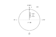
- FIG. 1 is a schematic plan view showing the configuration of a silicon wafer according to a first embodiment of the present invention.
- FIG. 2 is a schematic plan view showing the configuration of a silicon wafer according to a second embodiment of the present invention.
- FIG. 3 is a schematic view for explaining the types of warpage that occurs when a film stress is applied to a flat silicon wafer, where (a) is a bowl-shaped warpage and (b) is a bowl-shaped warpage. It shows.
- FIG. 4 is a schematic view for explaining the difference in how the wafer warps due to the film stress applied to the silicon wafer.
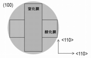
- FIG. 5 is a schematic perspective view showing an example of a film formation pattern for applying anisotropic film stress to a silicon wafer.
- FIG. 1 is a schematic plan view showing the configuration of a silicon wafer according to a first embodiment of the present invention.
- this silicon wafer 1A has a multilayer film forming a semiconductor device layer such as a 3D NAND flash memory on one main surface in the device process, and isotropy due to isotropic film stress due to the multilayer film. It is a silicon wafer for highly stacked semiconductor devices that is warped in a plane orientation of (111) and a notch orientation of ⁇ 110> or ⁇ 112>. That is, the notch 2 is formed in the ⁇ 110> or ⁇ 112> direction.
- the oxygen concentration of the silicon wafer 1A is preferably 8.0 ⁇ 10 17 atoms / cm 3 or more (ASTM F 121, 1979). (111)
- the Young's modulus of the silicon wafer has oxygen concentration dependency, and the warpage suppressing effect can be enhanced when the oxygen concentration is 8.0 ⁇ 10 17 atoms / cm 3 or more.
- FIG. 2 is a schematic plan view showing the configuration of a silicon wafer according to a second embodiment of the present invention.
- a multilayer film forming a semiconductor device layer is formed on one main surface in the device process, and high integration is obtained that warps in a wedge shape due to anisotropic film stress by the multilayer film.
- a silicon wafer for a semiconductor device having a plane orientation of (110) and a notch orientation of ⁇ 111>. That is, the notch 2 is formed in the ⁇ 111> direction.
- the oxygen concentration of the silicon wafer 1B is preferably 6.0 ⁇ 10 17 atoms / cm 3 or more (ASTM F 121, 1979). (110)
- the Young's modulus of the silicon wafer has oxygen concentration dependency, and the warpage suppressing effect can be enhanced when the oxygen concentration is 6.0 ⁇ 10 17 atoms / cm 3 or more.
- FIG. 3 is a schematic view for explaining the types of warpage that occurs when a film stress is applied to a flat silicon wafer, where (a) is a bowl-shaped warpage and (b) is a bowl-shaped warpage. It shows.
- the bowl shape refers to a shape in which the entire periphery of the outer peripheral portion of the wafer is displaced upward or downward from the central portion.
- either one of the X-direction and Y-direction ends of the wafer is displaced upward (or downward) from the central portion, and the other X-direction or Y-direction end of the wafer is the center. It refers to the shape displaced below (or above) the part.
- the bowl shape refers to a shape in which the entire periphery of the outer peripheral portion of the wafer is displaced upward or downward from the central portion.
- the wedge type either one of the X-direction and Y-direction ends of the wafer is displaced upward (or downward) from the central portion, and the other X-direction or Y-direction end of the wafer is the center. It refers to the shape displaced below (or above) the part.
- FIG. 4 is a schematic view for explaining the difference in how the wafer warps due to the film stress applied to the silicon wafer.
- the silicon wafer is warped during the device process because the sign of the film stress of the film formed on the silicon wafer is different to cause anisotropy of the film stress. For example, as shown in FIG. 4, when a wiring layer having a tensile stress in the Y direction orthogonal to the X direction is formed in addition to the wiring layer in which the compressive stress in the X direction is dominant, the compressive stress in the X direction is emphasized.
- the silicon wafer is warped into a bowl shape.
- the Young's modulus of silicon crystal differs depending on the crystal orientation, and has orientation dependency. It is 130 MPa in the [100] direction, 170 MPa in the [110] direction, and 189 MPa in the [111] direction, and the smaller the Young's modulus, the easier it is to deform.
- the direction in which the warpage is maximized coincides with the direction in which the Young's modulus of the crystal orientation is smaller, warpage is further facilitated, and the warpage amount is increased.
- the direction in which the warpage is maximum coincides with the direction in which the Young's modulus of the crystal orientation is large, warpage is further difficult, and the warpage amount decreases.
- the silicon wafer 1B having a plane orientation with a large orientation dependency of warpage of (110) and a notch orientation of ⁇ 111> is used.
- semiconductor devices are formed in accordance with the notch orientation in the device process, so that the direction in which the warpage of the wafer is large matches the direction in which the Young's modulus of the crystal orientation is large by aligning the direction of the wiring layer with the notch orientation. It is possible to enhance the effect of suppressing the warpage of the bowl shape.
- the silicon wafer 1A having a plane orientation (111) with no orientation dependency of warpage is used (see FIG. 1).
- the Young's modulus of the silicon wafer is isotropic in accordance with the isotropic film stress applied in the device process, the effect of suppressing the warp of the bowl shape can be enhanced.
- the present invention is not limited to such an example, and various methods in which the wafer is warped by film stress
- Example 1 Samples # 1 to # 16 of silicon wafers having different plane orientations and notch orientations were prepared. Each wafer is grown by the CZ method, and has a diameter of 300 mm and a thickness of 775 ⁇ m. There are three types of (100), (110), and (111) plane orientations of the wafer sample, and two kinds of ⁇ 110> and ⁇ 100> notch orientations of the plane orientation (100) wafer, plane orientation (110) wafer. The notch orientation of ⁇ 110> and ⁇ 111> is two types, and the notch orientation of the plane orientation (111) wafer is two types of ⁇ 110> and ⁇ 112>. The variation of the plane orientation and notch orientation of the used wafer is within ⁇ 1 degree.
- the oxygen concentration of each wafer was measured.
- the oxygen concentrations are all measured values by Fourier transform infrared spectroscopy (FT-IR) specified in ASTM F121, 1979.
- the amount of warpage was suppressed more than the wafers of the plane orientation (100) and (110) regardless of the notch orientation.
- the warpage of the wafer was dependent on oxygen concentration, and the warpage suppressing effect was particularly high when the oxygen concentration was 8.0 ⁇ 10 17 atoms / cm 3 or more. It is considered that the increase in oxygen concentration is an effect of improving the Young's modulus of the silicon crystal.
- Example 2 Similar to Example 1, samples # 17 to # 31 of silicon wafers having different plane orientations and notch orientations were prepared, and the oxygen concentration of these wafers was measured.
- a silicon oxide film with a thickness of 1 ⁇ m is formed by a CVD process, and then a part is etched using a mask, and then silicon with a thickness of 0.7 ⁇ m
- a nitride film was formed by a CVD process, a part was etched using a mask to produce a film having a shape as shown in FIG.
- the silicon oxide film is a rectangular pattern elongated in the ⁇ 110> direction
- the silicon nitride film is a rectangular pattern elongated in the direction orthogonal to the longitudinal direction of the silicon oxide film.
- the warpage amount changes depending on the oxygen concentration of the substrate and the notch direction, and it was found that the warpage suppressing effect of the ⁇ 111> notch is particularly high. Furthermore, among the wafer samples # 24 to # 27 of the ⁇ 111> notch, the warpage suppressing effect of the samples # 25, # 26, and # 27 in which the oxygen concentration is 6 ⁇ 10 17 atoms / cm 3 or more was particularly high.
Landscapes
- Chemical & Material Sciences (AREA)
- Engineering & Computer Science (AREA)
- Materials Engineering (AREA)
- Metallurgy (AREA)
- Organic Chemistry (AREA)
- Crystallography & Structural Chemistry (AREA)
- Inorganic Chemistry (AREA)
- General Chemical & Material Sciences (AREA)
- Chemical Kinetics & Catalysis (AREA)
- Mechanical Engineering (AREA)
- Semiconductor Memories (AREA)
- Non-Volatile Memory (AREA)
- Crystals, And After-Treatments Of Crystals (AREA)
- Formation Of Insulating Films (AREA)
Abstract
【課題】デバイス工程中に生じるウェーハの反りを低減し、ウェーハが大きく反ることによって不具合が有った後続工程を問題なく実施することが可能なシリコンウェーハを提供する。 【解決手段】本発明によるシリコンウェーハは、デバイス工程で一方の主面に半導体デバイス層を構成する多層膜が形成され、前記多層膜による等方性の膜応力によってお椀型に反るシリコンウェーハであって、シリコンウェーハの面方位は(111)である。
Description
本発明は、半導体デバイスの基板材料となるシリコンウェーハに関し、特に、3次元NANDフラッシュメモリ(以下、「3DNAND」という)等の高積層型半導体デバイスの基板材料として好適なシリコンウェーハ及びその加工方法に関するものである。
最近3DNANDが注目されている。3DNANDはメモリセルアレイを縦方向に積層化したNANDメモリであり、積層数(ワード線の層数)を例えば64層とすることでシングルダイ当たり512Gbit(64GB)という非常に大きな記憶容量を実現可能である。また従来のプレーナ型のNANDメモリのように平面方向の密度を上げるのではなく、高さ方向の密度を上げることによって大容量化のみならず書き込み速度の向上や省電力化にも優れた高性能なフラッシュメモリを提供することができる。
半導体デバイスの製造ではデバイス構造を形成するために酸化膜、窒化膜、金属膜等の様々な材料の膜がシリコンウェーハ上に積層される。このような積層膜は、膜の性質と工程条件によって異なる膜応力を有することになり、積層膜の膜応力によってシリコンウェーハには反りが発生する。特に、3DNANDでは個々のメモリ素子を垂直に数十個以上重ねて作るため、それに伴い積層膜の数も幾何学的に増えてくることで、それに比例して膜応力も膨大に増加してシリコンウェーハの反りも大きく増加する。デバイス工程中にシリコンウェーハが大きく反ることで、成膜、加工、検査などの後続工程での処理が出来ない等の不具合が生じてしまう。
3層以上の配線層を有する半導体装置の製造に関して、例えば特許文献1には、製造装置に依存せずかつ特殊層間膜の工程を用いることなく、シリコン基板の反りを所定値以下に抑えることが可能な半導体装置の製造方法が記載されている。この製造方法では、シリコン基板の厚さをT(μm)、直径をD(インチ)とし、配線層数をnとして、
T≧62.4×D×[1.6(n-1)+1.0]1/2
を満足する厚さを満足するシリコン基板を用いて半導体装置を製造する。
T≧62.4×D×[1.6(n-1)+1.0]1/2
を満足する厚さを満足するシリコン基板を用いて半導体装置を製造する。
また特許文献2、3には、中央部が凹んだお椀状の反りが付与されたエピタキシャル成長用シリコンウェーハの表面にエピタキシャル層を形成することにより、平坦度の高いエピタキシャルシリコンウェーハを製造する方法が記載されている。
しかしながら、特許文献1に記載の半導体装置の製造方法は、配線層の膜応力が変わらないことを前提にしておりその工程依存性を無視している。実際には工程条件によって膜応力が変動しているので、単純に配線層数だけで反り量を評価することはできず、適用が難しい。また12インチシリコンウェーハにおいて配線層数を500層とする場合、上記計算式によればシリコンウェーハの厚さT≧777.1μmを満足すればよいことになるが、これは12インチウェーハの標準の厚さである775μmと殆ど変わらず、反りを抑える効果が見込めないことは明らかである。
また、特許文献2、3に記載の技術は、エピタキシャル成長後のウェーハの反りを低減するために予め反りを持った初期ウェーハを形成する方法であって、デバイス工程中のウェーハの反りを低減するものではない。すなわち、このようなエピタキシャルウェーハに半導体デバイス層を形成することによってウェーハが反ったとしてもエピタキシャルウェーハ自体が反りを低減することはできない。またエピタキシャル成長工程をデバイス工程の一部と見做したとしても、低減しようとする反り量に対して作り込む形状の反り量を計算する方法については明らかで無い。また、ウェーハがお椀状に反る場合のみで、鞍型に反るウェーハの場合には適用できない。
シリコンウェーハの厚さ、形状、結晶方位などの仕様は、事前に反り量や反り形状とは関係なく規定されている。そのため、デバイス工程中にシリコンウェーハの反りが発生してもシリコンウェーハの仕様変更の基準がなく、ウェーハの反りに対応することはできなかった。
したがって、本発明の目的は、3DNAND等の半導体デバイスの製造工程中に生じるウェーハの反りを低減し、ウェーハが大きく反ることによって不具合が有った後続工程を問題なく実施することが可能なシリコンウェーハ及びその加工方法を提供することにある。
上記課題を解決するため、本発明によるシリコンウェーハは、デバイス工程で一方の主面に半導体デバイス層を構成する多層膜が形成され、前記多層膜の等方性の膜応力によってお椀型に反るシリコンウェーハであって、面方位が(111)であることを特徴とする。
デバイス工程中にウェーハがお椀型に反る場合に、反りの方位依存性が小さい(111)シリコンウェーハを使用することにより、お椀型の反りを抑制する効果を高めることができる。したがって、ウェーハが大きく反ることによって不具合が有った後続工程を問題なく実施することが可能なシリコンウェーハを提供することができる。
本発明によるシリコンウェーハの酸素濃度は8.0×10¹⁷atoms/cm3以上(ASTM F121,1979)であることが好ましい。結晶中の酸素濃度が高くなることでシリコン結晶のヤング率が向上するので、反り抑制効果を高めることができる。
本発明において、前記半導体デバイス層は3DNANDフラッシュメモリを含むことが好ましい。上記のように、3DNANDフラッシュメモリはメモリセルアレイの積層数が非常に多いためウェーハの反りの問題が顕著である。すなわち、デバイス工程が進んで積層数が増加するとウェーハの反りも徐々に増加し、最上層に到達する前にウェーハの反り量が許容範囲を超えてこれ以上デバイス工程を進めることができなくなる事態が生じる。しかし本発明によれば、デバイスを形成する前のウェーハの段階からウェーハの反りを押さえ込む対策を講じることで反りの問題を改善することができ、デバイス工程を進めることが出来なくなる事態を回避することができる。
また、本発明によるシリコンウェーハは、デバイス工程で一方の主面に半導体デバイス層を構成する多層膜が形成され、前記多層膜の異方性の膜応力によって鞍型に反るシリコンウェーハであって、面方位が(110)であり、ノッチ方位が<111>であることを特徴とする。
デバイス工程中にウェーハが鞍型に反る場合に、反りの方位依存性が大きい面方位が(110)であってノッチ方位が<111>のシリコンウェーハを使用することにより、ウェーハの反りが大きくなる方向と結晶方位のヤング率が大きい方向とを一致させることができ、これにより鞍型の反りを抑制する効果を高めることができる。したがって、ウェーハが大きく反ることによって不具合が有った後続工程を問題なく実施することが可能なシリコンウェーハを提供することができる。
本発明によるシリコンウェーハの酸素濃度は6.0×10¹⁷atoms/cm3以上(ASTM F121,1979)であることが好ましい。結晶中の酸素濃度が高くなることでシリコン結晶のヤング率が向上するので、反り抑制効果を高めることができる。
本発明において、前記半導体デバイス層は3DNANDフラッシュメモリを含むことが好ましい。上記のように、3DNANDフラッシュメモリはメモリセルアレイの積層数が非常に多いためウェーハの反りの問題が顕著である。すなわち、デバイス工程が進んで積層数が増加するとウェーハの反りも徐々に増加し、最上層に到達する前にウェーハの反り量が許容範囲を超えてこれ以上デバイス工程を進めることができなくなる事態が生じる。しかし本発明によれば、デバイスを形成する前のウェーハの段階からウェーハの反りを押さえ込む対策を講じることで反りの問題を改善することができ、デバイス工程を進めることが出来なくなる事態を回避することができる。
本発明によるシリコンウェーハの加工方法は、面方位が(111)のシリコンウェーハを用意し、前記シリコンウェーハの一方の主面に半導体デバイス層を構成する多層膜を形成すると共に、前記多層膜による等方性の膜応力によって生じるお椀型の反りを抑制することを特徴とする。本発明によれば、デバイス工程において膜応力によるウェーハの反りを抑制することができる。
また、本発明によるシリコンウェーハの加工方法は、面方位が(110)でノッチ方位が<111>のシリコンウェーハを用意し、前記シリコンウェーハの一方の主面に半導体デバイス層を構成する多層膜を形成すると共に、前記多層膜による異方性の膜応力によって生じる鞍型の反りの向きを前記ノッチ方位に合わせて前記鞍型の反りを抑制することを特徴とする。本発明によれば、デバイス工程において膜応力によるウェーハの反りを抑制することができる。
本発明によれば、デバイス工程中に生じるウェーハの反りを低減することができ、ウェーハが大きく反ることによって不具合が有った後続工程を問題なく実施することが可能なシリコンウェーハの製造方法を提供することができる。
以下、添付図面を参照しながら、本発明の好ましい実施の形態について詳細に説明する。
図1は、本発明の第1の実施の形態によるシリコンウェーハの構成を示す略平面図である。
図1に示すように、このシリコンウェーハ1Aは、デバイス工程で一方の主面に3DNANDフラッシュメモリなどの半導体デバイス層を構成する多層膜が形成され、多層膜による等方性の膜応力によってお椀型に反る高積層型半導体デバイス用シリコンウェーハであって、面方位が(111)であり、ノッチ方位が<110>又は<112>である。すなわち、ノッチ2は<110>又は<112>方向に形成されている。
シリコンウェーハ1Aの酸素濃度は8.0×10¹⁷atoms/cm3以上(ASTM F121,1979)であることが好ましい。(111)シリコンウェーハのヤング率には酸素濃度依存性があり、酸素濃度が8.0×10¹⁷atoms/cm3以上のときの反り抑制効果を高めることができる。
図2は、本発明の第2の実施の形態によるシリコンウェーハの構成を示す略平面図である。
図2に示すように、このシリコンウェーハ1Bは、デバイス工程で一方の主面に半導体デバイス層を構成する多層膜が形成され、多層膜による異方性の膜応力によって鞍型に反る高集積半導体デバイス用シリコンウェーハであって、面方位が(110)であり、ノッチ方位が<111>である。すなわち、ノッチ2は<111>方向に形成されている。
シリコンウェーハ1Bの酸素濃度は6.0×10¹⁷atoms/cm3以上(ASTM F121,1979)であることが好ましい。(110)シリコンウェーハのヤング率には酸素濃度依存性があり、酸素濃度が6.0×10¹⁷atoms/cm3以上のときの反り抑制効果を高めることができる。
図3は、平坦なシリコンウェーハに膜応力を付与したときに生じる反りの種類を説明するための模式図であって、(a)はお椀型の反り、(b)は鞍型の反りをそれぞれ示している。
シリコンウェーハの反り方にはお椀型と鞍型の2種類がある。平坦なシリコンウェーハに膜応力を付与したとき、等方性の膜応力であれば図3(a)に示すようにお椀型の反りが発生し、異方性の膜応力であれば図3(b)に示すように鞍型の反りが発生する。ここで、お椀型とは、ウェーハの外周部の全周が中央部よりも上方又は下方に変位した形状のことをいう。また鞍型とは、ウェーハのX方向及びY方向のいずれか一方の両端部が中央部よりも上方(又は下方)に変位し、ウェーハのX方向及びY方向のいずれか他方の両端部が中央部よりも下方(又は上方)に変位した形状のことをいう。
お椀型とは、ウェーハの外周部の全周が中央部よりも上方又は下方に変位した形状のことをいう。また鞍型とは、ウェーハのX方向及びY方向のいずれか一方の両端部が中央部よりも上方(又は下方)に変位し、ウェーハのX方向及びY方向のいずれか他方の両端部が中央部よりも下方(又は上方)に変位した形状のことをいう。
図4は、シリコンウェーハに付与される膜応力によるウェーハの反り方の違いを説明するための模式図である。
図4に示すように、シリコンウェーハの表面に半導体デバイスを構成する配線層等の積層膜を成膜すると、当該シリコンウェーハに膜応力が生じ、これにより(a)に示すようなお椀型の反り、或いは(b)に示すような鞍型の反りが発生する。このようなウェーハの反りが大きくなると後続工程で様々な問題が生じる。
デバイス工程中にシリコンウェーハが鞍型に反る理由は、シリコンウェーハ上に形成される膜の膜応力の符号が違うことで膜応力の異方性が生じるからである。例えば、図4に示すように、X方向の圧縮応力が支配的な配線層に加えて、X方向と直交するY方向に引張応力を有する配線層を成膜すると、X方向の圧縮応力が強調され、シリコンウェーハは鞍型に反ることになる。
シリコン結晶のヤング率は結晶方位によって異なり、方位依存性を持っている。[100]方向では130MPa、[110]方向では170MPa、[111]方向では189MPaであり、ヤング率が小さい方が変形しやすくなる。ウェーハが鞍型に反る場合において、反りが最大となる方向が結晶方位のヤング率が小さい方向と一致すればさらに反りやすくなり、反り量は増加することになる。反対に、反りが最大となる方向が結晶方位のヤング率が大きい方向と一致すればさらに反りにくくなり、反り量は減少することになる。
そこで本実施形態においては、デバイス工程中にウェーハが鞍型に反る場合には、反りの方位依存性が大きい面方位が(110)であってノッチ方位が<111>のシリコンウェーハ1Bを用いる(図2参照)。通常、デバイス工程ではノッチ方位に合わせて半導体デバイスを形成するので、配線層の向きをノッチ方位に合わせることでウェーハの反りが大きくなる方向と結晶方位のヤング率が大きい方向とを一致させることができ、鞍型の反りを抑制する効果を高めることができる。
またデバイス工程中にウェーハがお椀型に反る場合には、反りの方位依存性がない面方位が(111)のシリコンウェーハ1Aを用いる(図1参照)。デバイス工程で付与される等方性の膜応力に合わせてシリコンウェーハのヤング率も等方性とすることで、お椀型の反りを抑制する効果を高めることができる。
以上、本発明の好ましい実施形態について説明したが、本発明は、上記の実施形態に限定されることなく、本発明の主旨を逸脱しない範囲で種々の変更が可能であり、それらも本発明の範囲内に包含されるものであることはいうまでもない。
例えば、上記実施形態においては、3DNANDの製造に好適なシリコンウェーハの製造方法について説明したが、本発明はこのような例に限定されるものではなく、膜応力によってウェーハが反ることとなる種々の半導体デバイス用のシリコンウェーハを対象とすることができる。
(実施例1)
面方位及びノッチ方位が異なるシリコンウェーハのサンプル#1~#16を用意した。各ウェーハはCZ法で育成されたものであり、直径は300mm、厚みは775μmである。ウェーハサンプルの面方位は(100)、(110)、(111)の3種類であり、面方位(100)ウェーハのノッチ方位は<110>と<100>の2種類、面方位(110)ウェーハのノッチ方位は<110>と<111>の2種類、面方位(111)ウェーハのノッチ方位は<110>と<112>の2種類である。使用したウェーハの面方位及びノッチ方位のばらつきは±1度以内である。
面方位及びノッチ方位が異なるシリコンウェーハのサンプル#1~#16を用意した。各ウェーハはCZ法で育成されたものであり、直径は300mm、厚みは775μmである。ウェーハサンプルの面方位は(100)、(110)、(111)の3種類であり、面方位(100)ウェーハのノッチ方位は<110>と<100>の2種類、面方位(110)ウェーハのノッチ方位は<110>と<111>の2種類、面方位(111)ウェーハのノッチ方位は<110>と<112>の2種類である。使用したウェーハの面方位及びノッチ方位のばらつきは±1度以内である。
次に各ウェーハの酸素濃度を測定した。なお酸素濃度はすべてASTM F121,1979に規格されたフーリエ変換赤外分光光度法(FT-IR)による測定値である。
次に、これらのウェーハサンプル#1~#16の主面に、厚みが2μmのシリコン酸化膜をCVD工程で成膜したところ、凸状のお椀型の反りをもたらした。各ウェーハサンプルの反り量(WARP)の測定結果を表1に示す。

表1から明らかなように、面方位(100)のウェーハサンプル#1~#4では、基板酸素濃度やノッチ方位によらず、600μm程度の大きな反りが発生した。
面方位(110)のウェーハサンプル#5~#8では、基板酸素濃度、ノッチ方位によらず、770μm程度の大きな反りが発生した。酸素濃度が高いほど反り量が減少するが、大きな差はない。
面方位(111)のウェーハサンプル#9~#16では、ノッチ方位によらず、面方位(100)や(110)のウェーハよりも反り量が抑制されることが分かった。またウェーハの反りには酸素濃度依存性があり、酸素濃度が8.0×10¹⁷atoms/cm3以上のときの反り抑制効果が特に高かった。酸素濃度が高くなることでシリコン結晶のヤング率が向上する効果だと考えられる。
シリコン結晶のヤング率は結晶方位によって異なる方位依存性を持っているため、お椀型に反るような異方性が少ない膜応力が付与されると、面方位によって弾性変形に対する耐性が変化すると思われる。以上の結果から、(111)ウェーハを用いることで、デバイス工程で問題となる反りを抑制することが可能である。
(実施例2)
実施例1と同様に面方位及びノッチ方位が異なるシリコンウェーハのサンプル#17~#31を用意し、それらのウェーハの酸素濃度を測定した。
実施例1と同様に面方位及びノッチ方位が異なるシリコンウェーハのサンプル#17~#31を用意し、それらのウェーハの酸素濃度を測定した。
次に、これらのウェーハサンプル#17~#31の主面に、厚みが1μmのシリコン酸化膜をCVD工程で成膜した後にマスクを利用して一部をエッチングし、次いで厚み0.7μmのシリコン窒化膜をCVD工程で成膜した後にマスクを利用して一部をエッチングして、図5のような形状の膜を作製した。例えばサンプル#17の(100)ウェーハの場合、シリコン酸化膜は<110>方位に細長い矩形パターンであり、シリコン窒化膜はシリコン酸化膜の長手方向と直交する方向に細長い矩形パターンである。この合成パターンにより、シリコンウェーハには異方性の膜応力が発生し、鞍型の反りをもたらした。各ウェーハサンプルの反り量(WARP)の測定結果を表2に示す。

表2から明らかなように、面方位(100)のウェーハサンプル#17~#20では、基板酸素濃度やノッチ方位によって反り量が変化し、特に<100>ノッチよりも<110>ノッチのほうが反り抑制効果が高いことが分かった。ただし(100)ウェーハの<110>ノッチはウェーハの標準的な方位である。
面方位(110)のウェーハサンプル#21~#27では、基板酸素濃度やノッチ方位によって反り量が変化し、特に<111>ノッチの反り抑制効果が高いことが分かった。さらに、<111>ノッチのウェーハサンプル#24~#27の中でも、酸素濃度が6×10¹⁷atoms/cm3以上となるサンプル#25、#26、#27の反り抑制効果は特に高かった。
面方位(111)のウェーハサンプル#28~#31では、基板酸素濃度やノッチ方位によらず、500μm程度の大きな反りが発生した。ただし(111)ウェーハの<110>ノッチはウェーハの標準的な方位である。
1A,1B シリコンウェーハ
2 ノッチ
2 ノッチ
Claims (6)
- デバイス工程で一方の主面に半導体デバイス層を構成する多層膜が形成され、前記多層膜の等方性の膜応力によってお椀型に反るシリコンウェーハであって、面方位が(111)であることを特徴とするシリコンウェーハ。
- 酸素濃度が8.0×10¹⁷atoms/cm3以上(ASTM F121,1979)である、請求項1に記載のシリコンウェーハ。
- 前記半導体デバイス層は3DNANDフラッシュメモリを含む、請求項1又は2に記載のシリコンウェーハ。
- デバイス工程で一方の主面に半導体デバイス層を構成する多層膜が形成され、前記多層膜の異方性の膜応力によって鞍型に反るシリコンウェーハであって、面方位が(110)であり、ノッチ方位が<111>であることを特徴とするシリコンウェーハ。
- 酸素濃度が6.0×10¹⁷atoms/cm3以上(ASTM F121,1979)である、請求項4に記載のシリコンウェーハ。
- 前記半導体デバイス層は3DNANDフラッシュメモリを含む、請求項4又は5に記載のシリコンウェーハ。
Priority Applications (4)
| Application Number | Priority Date | Filing Date | Title |
|---|---|---|---|
| CN201880046219.1A CN111164240B (zh) | 2017-07-10 | 2018-06-06 | 硅晶片 |
| US16/619,143 US20200176461A1 (en) | 2017-07-10 | 2018-06-06 | Silicon wafer |
| KR1020197035098A KR102331580B1 (ko) | 2017-07-10 | 2018-06-06 | 실리콘 웨이퍼 |
| US17/541,767 US12004344B2 (en) | 2017-07-10 | 2021-12-03 | Method of reducing wrap imparted to silicon wafer by semiconductor layers |
Applications Claiming Priority (2)
| Application Number | Priority Date | Filing Date | Title |
|---|---|---|---|
| JP2017-134918 | 2017-07-10 | ||
| JP2017134918A JP6834816B2 (ja) | 2017-07-10 | 2017-07-10 | シリコンウェーハの加工方法 |
Related Child Applications (2)
| Application Number | Title | Priority Date | Filing Date |
|---|---|---|---|
| US16/619,143 A-371-Of-International US20200176461A1 (en) | 2017-07-10 | 2018-06-06 | Silicon wafer |
| US17/541,767 Continuation US12004344B2 (en) | 2017-07-10 | 2021-12-03 | Method of reducing wrap imparted to silicon wafer by semiconductor layers |
Publications (1)
| Publication Number | Publication Date |
|---|---|
| WO2019012867A1 true WO2019012867A1 (ja) | 2019-01-17 |
Family
ID=65001991
Family Applications (1)
| Application Number | Title | Priority Date | Filing Date |
|---|---|---|---|
| PCT/JP2018/021721 Ceased WO2019012867A1 (ja) | 2017-07-10 | 2018-06-06 | シリコンウェーハ |
Country Status (6)
| Country | Link |
|---|---|
| US (2) | US20200176461A1 (ja) |
| JP (1) | JP6834816B2 (ja) |
| KR (1) | KR102331580B1 (ja) |
| CN (1) | CN111164240B (ja) |
| TW (1) | TWI682524B (ja) |
| WO (1) | WO2019012867A1 (ja) |
Citations (3)
| Publication number | Priority date | Publication date | Assignee | Title |
|---|---|---|---|---|
| JP2012039117A (ja) * | 2010-08-11 | 2012-02-23 | Siltronic Ag | シリコンウェハおよびシリコンウェハの製造方法 |
| WO2013137476A1 (ja) * | 2012-03-16 | 2013-09-19 | 次世代パワーデバイス技術研究組合 | 半導体積層基板、半導体素子、およびその製造方法 |
| JP2015088706A (ja) * | 2013-11-01 | 2015-05-07 | 大日本印刷株式会社 | エッチングマスクの設計方法、構造体の製造方法及びエッチングマスク |
Family Cites Families (18)
| Publication number | Priority date | Publication date | Assignee | Title |
|---|---|---|---|---|
| JPH0529324A (ja) * | 1991-07-22 | 1993-02-05 | Mitsubishi Materials Corp | シリコンウエーハの製造方法 |
| JPH09266206A (ja) | 1996-03-28 | 1997-10-07 | Nec Corp | 半導体装置の製造方法およびシリコン基板 |
| JPH1032233A (ja) * | 1996-07-15 | 1998-02-03 | Seiko Epson Corp | シリコンウェーハ、ガラスウェーハ及びそれを用いたストレス測定方法 |
| US7052974B2 (en) * | 2001-12-04 | 2006-05-30 | Shin-Etsu Handotai Co., Ltd. | Bonded wafer and method of producing bonded wafer |
| US7262112B2 (en) | 2005-06-27 | 2007-08-28 | The Regents Of The University Of California | Method for producing dislocation-free strained crystalline films |
| US7902039B2 (en) * | 2006-11-30 | 2011-03-08 | Sumco Corporation | Method for manufacturing silicon wafer |
| JP5250968B2 (ja) | 2006-11-30 | 2013-07-31 | 株式会社Sumco | エピタキシャルシリコンウェーハ及びその製造方法並びにエピタキシャル成長用シリコンウェーハ。 |
| US7816765B2 (en) * | 2008-06-05 | 2010-10-19 | Sumco Corporation | Silicon epitaxial wafer and the production method thereof |
| JP5625229B2 (ja) | 2008-07-31 | 2014-11-19 | 株式会社Sumco | エピタキシャルシリコンウェーハおよびその製造方法 |
| JP5537802B2 (ja) * | 2008-12-26 | 2014-07-02 | ジルトロニック アクチエンゲゼルシャフト | シリコンウエハの製造方法 |
| US8084822B2 (en) * | 2009-09-30 | 2011-12-27 | International Business Machines Corporation | Enhanced stress-retention fin-FET devices and methods of fabricating enhanced stress retention fin-FET devices |
| CN102208337B (zh) * | 2010-03-30 | 2014-04-09 | 杭州海鲸光电科技有限公司 | 一种硅基复合衬底及其制造方法 |
| US20120064682A1 (en) * | 2010-09-14 | 2012-03-15 | Jang Kyung-Tae | Methods of Manufacturing Three-Dimensional Semiconductor Memory Devices |
| US8625083B2 (en) * | 2011-03-12 | 2014-01-07 | Ken Roberts | Thin film stress measurement 3D anisotropic volume |
| CN102354664B (zh) * | 2011-09-28 | 2015-12-16 | 上海华虹宏力半导体制造有限公司 | 金属间介质层形成方法及半导体器件 |
| JP6156188B2 (ja) * | 2014-02-26 | 2017-07-05 | 株式会社Sumco | エピタキシャルシリコンウェーハの製造方法 |
| US9490116B2 (en) * | 2015-01-09 | 2016-11-08 | Applied Materials, Inc. | Gate stack materials for semiconductor applications for lithographic overlay improvement |
| CN105448666A (zh) * | 2015-12-02 | 2016-03-30 | 苏州工业园区纳米产业技术研究院有限公司 | 利用二氧化硅的应力来改变晶圆硅片基体弯曲度的方法 |
-
2017
- 2017-07-10 JP JP2017134918A patent/JP6834816B2/ja active Active
-
2018
- 2018-06-06 CN CN201880046219.1A patent/CN111164240B/zh active Active
- 2018-06-06 US US16/619,143 patent/US20200176461A1/en not_active Abandoned
- 2018-06-06 WO PCT/JP2018/021721 patent/WO2019012867A1/ja not_active Ceased
- 2018-06-06 KR KR1020197035098A patent/KR102331580B1/ko active Active
- 2018-06-19 TW TW107120956A patent/TWI682524B/zh active
-
2021
- 2021-12-03 US US17/541,767 patent/US12004344B2/en active Active
Patent Citations (3)
| Publication number | Priority date | Publication date | Assignee | Title |
|---|---|---|---|---|
| JP2012039117A (ja) * | 2010-08-11 | 2012-02-23 | Siltronic Ag | シリコンウェハおよびシリコンウェハの製造方法 |
| WO2013137476A1 (ja) * | 2012-03-16 | 2013-09-19 | 次世代パワーデバイス技術研究組合 | 半導体積層基板、半導体素子、およびその製造方法 |
| JP2015088706A (ja) * | 2013-11-01 | 2015-05-07 | 大日本印刷株式会社 | エッチングマスクの設計方法、構造体の製造方法及びエッチングマスク |
Also Published As
| Publication number | Publication date |
|---|---|
| JP2019014638A (ja) | 2019-01-31 |
| KR102331580B1 (ko) | 2021-11-25 |
| CN111164240B (zh) | 2021-12-28 |
| CN111164240A (zh) | 2020-05-15 |
| TWI682524B (zh) | 2020-01-11 |
| KR20190142388A (ko) | 2019-12-26 |
| TW201909391A (zh) | 2019-03-01 |
| JP6834816B2 (ja) | 2021-02-24 |
| US12004344B2 (en) | 2024-06-04 |
| US20220093624A1 (en) | 2022-03-24 |
| US20200176461A1 (en) | 2020-06-04 |
Similar Documents
| Publication | Publication Date | Title |
|---|---|---|
| KR102289163B1 (ko) | 실리콘 웨이퍼의 제조 방법 | |
| JP6777029B2 (ja) | シリコンウェーハ及びその製造方法 | |
| TWI669765B (zh) | 使用背面補償結構的晶圓平整度控制 | |
| TWI765874B (zh) | 用以改善晶圓平面性之方法及由其所製造之接合晶圓總成 | |
| US11227760B2 (en) | Wafer thinning method and wafer structure | |
| TWI353653B (en) | Patterned strained semiconductor substrate and dev | |
| CN112687524B (zh) | 一种晶圆弯曲度调整方法 | |
| TWI645454B (zh) | 磊晶基板及其製造方法 | |
| TW201222732A (en) | Methods for processing a semiconductor wafer, a semiconductor wafer and a semiconductor device | |
| WO2013046525A1 (ja) | 貼り合わせsoiウェーハの反りを算出する方法、及び貼り合わせsoiウェーハの製造方法 | |
| CN107564916A (zh) | 一种3d nand存储器件的平坦化方法 | |
| TW406302B (en) | Method of fabricating semiconductor substrate | |
| CN109585526A (zh) | 半导体衬底及其制造方法 | |
| US20200248304A1 (en) | Composite substrate and manufacturing method thereof | |
| WO2019012867A1 (ja) | シリコンウェーハ | |
| US12400981B2 (en) | Method for manufacturing semiconductor device | |
| KR102352511B1 (ko) | 실리콘에피택셜 웨이퍼의 제조방법 및 반도체 디바이스의 제조방법 | |
| CN107749397A (zh) | 一种晶圆减薄方法 | |
| TW201802881A (zh) | 用於製造用以形成三維單片積體電路之結構的方法 | |
| WO2008069606A1 (en) | Method of manufacturing integrated circuit having stacked structure and the integrated circuit | |
| CN104157579B (zh) | 一种多沟道全包围栅极的半导体器件结构的制备方法 | |
| CN118763058A (zh) | 一种便于晶圆划片的结构、方法及工艺 | |
| WO2024116506A1 (ja) | ヘテロエピタキシャル基板の製造方法 | |
| CN116322038A (zh) | 一种半导体结构的制备方法 |
Legal Events
| Date | Code | Title | Description |
|---|---|---|---|
| 121 | Ep: the epo has been informed by wipo that ep was designated in this application |
Ref document number: 18832857 Country of ref document: EP Kind code of ref document: A1 |
|
| ENP | Entry into the national phase |
Ref document number: 20197035098 Country of ref document: KR Kind code of ref document: A |
|
| NENP | Non-entry into the national phase |
Ref country code: DE |
|
| 122 | Ep: pct application non-entry in european phase |
Ref document number: 18832857 Country of ref document: EP Kind code of ref document: A1 |