WO2019004354A1 - 直接形電力変換器用制御装置 - Google Patents
直接形電力変換器用制御装置 Download PDFInfo
- Publication number
- WO2019004354A1 WO2019004354A1 PCT/JP2018/024578 JP2018024578W WO2019004354A1 WO 2019004354 A1 WO2019004354 A1 WO 2019004354A1 JP 2018024578 W JP2018024578 W JP 2018024578W WO 2019004354 A1 WO2019004354 A1 WO 2019004354A1
- Authority
- WO
- WIPO (PCT)
- Prior art keywords
- command
- value
- voltage
- current
- normalized
- Prior art date
Links
Images


Classifications
-
- H—ELECTRICITY
- H02—GENERATION; CONVERSION OR DISTRIBUTION OF ELECTRIC POWER
- H02M—APPARATUS FOR CONVERSION BETWEEN AC AND AC, BETWEEN AC AND DC, OR BETWEEN DC AND DC, AND FOR USE WITH MAINS OR SIMILAR POWER SUPPLY SYSTEMS; CONVERSION OF DC OR AC INPUT POWER INTO SURGE OUTPUT POWER; CONTROL OR REGULATION THEREOF
- H02M1/00—Details of apparatus for conversion
- H02M1/42—Circuits or arrangements for compensating for or adjusting power factor in converters or inverters
- H02M1/4208—Arrangements for improving power factor of AC input
- H02M1/4225—Arrangements for improving power factor of AC input using a non-isolated boost converter
-
- H—ELECTRICITY
- H02—GENERATION; CONVERSION OR DISTRIBUTION OF ELECTRIC POWER
- H02M—APPARATUS FOR CONVERSION BETWEEN AC AND AC, BETWEEN AC AND DC, OR BETWEEN DC AND DC, AND FOR USE WITH MAINS OR SIMILAR POWER SUPPLY SYSTEMS; CONVERSION OF DC OR AC INPUT POWER INTO SURGE OUTPUT POWER; CONTROL OR REGULATION THEREOF
- H02M3/00—Conversion of dc power input into dc power output
- H02M3/02—Conversion of dc power input into dc power output without intermediate conversion into ac
- H02M3/04—Conversion of dc power input into dc power output without intermediate conversion into ac by static converters
- H02M3/10—Conversion of dc power input into dc power output without intermediate conversion into ac by static converters using discharge tubes with control electrode or semiconductor devices with control electrode
- H02M3/145—Conversion of dc power input into dc power output without intermediate conversion into ac by static converters using discharge tubes with control electrode or semiconductor devices with control electrode using devices of a triode or transistor type requiring continuous application of a control signal
- H02M3/155—Conversion of dc power input into dc power output without intermediate conversion into ac by static converters using discharge tubes with control electrode or semiconductor devices with control electrode using devices of a triode or transistor type requiring continuous application of a control signal using semiconductor devices only
- H02M3/156—Conversion of dc power input into dc power output without intermediate conversion into ac by static converters using discharge tubes with control electrode or semiconductor devices with control electrode using devices of a triode or transistor type requiring continuous application of a control signal using semiconductor devices only with automatic control of output voltage or current, e.g. switching regulators
- H02M3/158—Conversion of dc power input into dc power output without intermediate conversion into ac by static converters using discharge tubes with control electrode or semiconductor devices with control electrode using devices of a triode or transistor type requiring continuous application of a control signal using semiconductor devices only with automatic control of output voltage or current, e.g. switching regulators including plural semiconductor devices as final control devices for a single load
-
- H—ELECTRICITY
- H02—GENERATION; CONVERSION OR DISTRIBUTION OF ELECTRIC POWER
- H02M—APPARATUS FOR CONVERSION BETWEEN AC AND AC, BETWEEN AC AND DC, OR BETWEEN DC AND DC, AND FOR USE WITH MAINS OR SIMILAR POWER SUPPLY SYSTEMS; CONVERSION OF DC OR AC INPUT POWER INTO SURGE OUTPUT POWER; CONTROL OR REGULATION THEREOF
- H02M7/00—Conversion of ac power input into dc power output; Conversion of dc power input into ac power output
- H02M7/42—Conversion of dc power input into ac power output without possibility of reversal
- H02M7/44—Conversion of dc power input into ac power output without possibility of reversal by static converters
- H02M7/48—Conversion of dc power input into ac power output without possibility of reversal by static converters using discharge tubes with control electrode or semiconductor devices with control electrode
- H02M7/53—Conversion of dc power input into ac power output without possibility of reversal by static converters using discharge tubes with control electrode or semiconductor devices with control electrode using devices of a triode or transistor type requiring continuous application of a control signal
- H02M7/537—Conversion of dc power input into ac power output without possibility of reversal by static converters using discharge tubes with control electrode or semiconductor devices with control electrode using devices of a triode or transistor type requiring continuous application of a control signal using semiconductor devices only, e.g. single switched pulse inverters
- H02M7/5387—Conversion of dc power input into ac power output without possibility of reversal by static converters using discharge tubes with control electrode or semiconductor devices with control electrode using devices of a triode or transistor type requiring continuous application of a control signal using semiconductor devices only, e.g. single switched pulse inverters in a bridge configuration
- H02M7/53871—Conversion of dc power input into ac power output without possibility of reversal by static converters using discharge tubes with control electrode or semiconductor devices with control electrode using devices of a triode or transistor type requiring continuous application of a control signal using semiconductor devices only, e.g. single switched pulse inverters in a bridge configuration with automatic control of output voltage or current
-
- H—ELECTRICITY
- H02—GENERATION; CONVERSION OR DISTRIBUTION OF ELECTRIC POWER
- H02M—APPARATUS FOR CONVERSION BETWEEN AC AND AC, BETWEEN AC AND DC, OR BETWEEN DC AND DC, AND FOR USE WITH MAINS OR SIMILAR POWER SUPPLY SYSTEMS; CONVERSION OF DC OR AC INPUT POWER INTO SURGE OUTPUT POWER; CONTROL OR REGULATION THEREOF
- H02M7/00—Conversion of ac power input into dc power output; Conversion of dc power input into ac power output
- H02M7/42—Conversion of dc power input into ac power output without possibility of reversal
- H02M7/44—Conversion of dc power input into ac power output without possibility of reversal by static converters
- H02M7/48—Conversion of dc power input into ac power output without possibility of reversal by static converters using discharge tubes with control electrode or semiconductor devices with control electrode
- H02M7/53—Conversion of dc power input into ac power output without possibility of reversal by static converters using discharge tubes with control electrode or semiconductor devices with control electrode using devices of a triode or transistor type requiring continuous application of a control signal
- H02M7/537—Conversion of dc power input into ac power output without possibility of reversal by static converters using discharge tubes with control electrode or semiconductor devices with control electrode using devices of a triode or transistor type requiring continuous application of a control signal using semiconductor devices only, e.g. single switched pulse inverters
- H02M7/539—Conversion of dc power input into ac power output without possibility of reversal by static converters using discharge tubes with control electrode or semiconductor devices with control electrode using devices of a triode or transistor type requiring continuous application of a control signal using semiconductor devices only, e.g. single switched pulse inverters with automatic control of output wave form or frequency
- H02M7/5395—Conversion of dc power input into ac power output without possibility of reversal by static converters using discharge tubes with control electrode or semiconductor devices with control electrode using devices of a triode or transistor type requiring continuous application of a control signal using semiconductor devices only, e.g. single switched pulse inverters with automatic control of output wave form or frequency by pulse-width modulation
-
- H—ELECTRICITY
- H02—GENERATION; CONVERSION OR DISTRIBUTION OF ELECTRIC POWER
- H02M—APPARATUS FOR CONVERSION BETWEEN AC AND AC, BETWEEN AC AND DC, OR BETWEEN DC AND DC, AND FOR USE WITH MAINS OR SIMILAR POWER SUPPLY SYSTEMS; CONVERSION OF DC OR AC INPUT POWER INTO SURGE OUTPUT POWER; CONTROL OR REGULATION THEREOF
- H02M1/00—Details of apparatus for conversion
- H02M1/0003—Details of control, feedback or regulation circuits
- H02M1/0025—Arrangements for modifying reference values, feedback values or error values in the control loop of a converter
-
- H—ELECTRICITY
- H02—GENERATION; CONVERSION OR DISTRIBUTION OF ELECTRIC POWER
- H02M—APPARATUS FOR CONVERSION BETWEEN AC AND AC, BETWEEN AC AND DC, OR BETWEEN DC AND DC, AND FOR USE WITH MAINS OR SIMILAR POWER SUPPLY SYSTEMS; CONVERSION OF DC OR AC INPUT POWER INTO SURGE OUTPUT POWER; CONTROL OR REGULATION THEREOF
- H02M1/00—Details of apparatus for conversion
- H02M1/0067—Converter structures employing plural converter units, other than for parallel operation of the units on a single load
- H02M1/007—Plural converter units in cascade
-
- Y—GENERAL TAGGING OF NEW TECHNOLOGICAL DEVELOPMENTS; GENERAL TAGGING OF CROSS-SECTIONAL TECHNOLOGIES SPANNING OVER SEVERAL SECTIONS OF THE IPC; TECHNICAL SUBJECTS COVERED BY FORMER USPC CROSS-REFERENCE ART COLLECTIONS [XRACs] AND DIGESTS
- Y02—TECHNOLOGIES OR APPLICATIONS FOR MITIGATION OR ADAPTATION AGAINST CLIMATE CHANGE
- Y02B—CLIMATE CHANGE MITIGATION TECHNOLOGIES RELATED TO BUILDINGS, e.g. HOUSING, HOUSE APPLIANCES OR RELATED END-USER APPLICATIONS
- Y02B70/00—Technologies for an efficient end-user side electric power management and consumption
- Y02B70/10—Technologies improving the efficiency by using switched-mode power supplies [SMPS], i.e. efficient power electronics conversion e.g. power factor correction or reduction of losses in power supplies or efficient standby modes
Definitions
- the present invention relates to a technique for controlling a direct power converter including a rectifier circuit, an inverter, and a power buffer circuit interconnected via a direct current link.
- the power obtained from a single-phase AC power source has pulsations with a frequency twice that of the power source frequency. Therefore, when rectifying a single phase AC voltage obtained from a single phase AC power supply to obtain a DC voltage, a large-capacity energy storage element is required to make the DC voltage constant.
- a technique has been proposed that employs a power buffer circuit in which a buffer capacitor is connected to a DC link via a switching element to thereby generate a voltage source (for example, Patent Document 1 below, Non-patent Document Literature 1).
- the voltage source can realize high efficiency characteristics by setting the waveform of the current input in the direct power converter that generates the high frequency link together with the voltage obtained from the single phase AC power supply to a sine wave.
- the DC voltage of the DC link can be increased to the peak value of the single-phase AC voltage (for example, Non-Patent Document 1).
- a practical value for example, a value 1.17 times the peak value is selected as the buffer voltage borne by the buffer capacitor, the voltage utilization factor remains at about 0.87.
- a control method has been proposed which improves the voltage utilization to 0.95 even with the same buffer voltage (for example, Patent Document 2 listed below).
- Patent Document 3 a control method focusing on the voltage output from the power converter has also been proposed (eg, Patent Document 3 and Non-Patent Document 1).
- the step-up operation is realized by increasing the proportion of steady-state power in the power shared by the power buffer circuit (power transferred to and from the DC link).
- Such a control method is effective in a voltage range in which the power to be shared does not increase significantly.
- Patent Document 4 is cited as an example of disclosing a technique for controlling the amplitude of the input current based on the buffer voltage.
- the power shared by the power buffer circuit is passively determined by other factors. Specifically, the magnitude of the power shared by the power buffer circuit is determined by determining the current supplied to the power buffer circuit so that the input current has a sine wave.
- a current detector for detecting the current in various places is required, and the control circuit is complicated. Invite.
- the present invention has been made in view of the above-described circumstances, and an object of the present invention is to provide a technology that does not require detection of current in control of a power buffer circuit.
- the direct power converter control device is a control device (10) that controls the direct power converter.
- the direct power converter performs full-wave rectification on a DC link (7) including a first power supply line (LH) and a second power supply line (LL), and a single phase AC voltage (Vin);
- a rectifier circuit (3) which outputs a pulsating power (Pin) to the DC link by setting one power supply line to a higher potential than the second power supply line, and between the first power supply line and the second power supply line
- an inverter (5) for converting the output voltage into an alternating voltage.
- the power buffer circuit includes a capacitor (C4), a discharge circuit (4a) for discharging the capacitor, and a charging circuit (4b) for charging the capacitor.
- the control device includes an inverter control unit (101), a normalized current command generation unit (102), and a buffer control unit (103).
- the inverter control unit (101) includes a rectification duty dr which is a duty that causes the rectification circuit to conduct to the DC link, a discharge duty dc which is a duty that the capacitor discharges, and a command value of a voltage which the inverter outputs
- An inverter control signal (SSg) for controlling the operation of the inverter is output based on Vu *, Vv *, Vw *).
- the normalized current command generation unit (102) is a command value of the current normalized by the amplitude (Im) of the input current (Iin) input to the rectifier circuit, the output current (irec) output from the rectifier circuit. Generates and outputs a normalized current command (
- the buffer control unit (103) includes an amplitude setting unit (103a), a charge command generation unit (103b), a charge operation control unit (103c), a discharge operation control unit (103d), and a normalized link current estimation unit (103e) and a calculation unit (103f).
- the amplitude setting unit (103a) determines the amplitude (Im of the input current) based on a deviation between an end-to-end voltage command (Vc *) which is a command value for an average value of the end-to-end voltage Vc of the capacitor and the end-to-end voltage Vc.
- the amplitude command (Im *) which is the command value of) is set.
- the charge command generation unit (103b) multiplies the amplitude command by the normalized charge command (ib * / Im *) to generate a charge command (ib *) which is a command value of the current (ib) flowing through the charge circuit. Do.
- the charge operation control unit (103c) controls the charge operation of the charge circuit based on the charge command.
- the discharge operation control unit (103d) discharges the capacitor based on the discharge duty dc.
- the normalized link current estimation unit (103e) is configured to calculate a virtual DC voltage command Vdc *, a phase ⁇ t and an amplitude Vm of the single-phase AC voltage, and a first value (J) calculated using the distribution factor k.
- a link current (Idc) flowing from the DC link to the inverter is adopted and output as an estimated value (Idc ⁇ / Im *) of a value normalized by the amplitude (Im) of the input current.
- the virtual DC voltage command Vdc * is a command value of a virtual DC voltage (Vdc).
- the virtual DC voltage (Vdc) is expressed by dr ⁇ Vrec + dc ⁇ Vc.
- the calculation unit (103f) obtains a second value (R) calculated using the virtual DC voltage command Vdc *, the rectified voltage Vrec output from the rectifier circuit, and the both-end voltage Vc. Then, if the normalized current command (
- the control of the power buffer circuit does not require the detection of current.
- FIG. 2 is a circuit diagram showing the configuration of a direct power converter to which the control technique described in this embodiment is applied.
- FIG. 2 is a circuit diagram showing an equivalent circuit of the direct power converter shown in FIG. 1;
- FIG. 2 is a block diagram illustrating the configuration of a control device.
- the flowchart which shows the setting of rectification
- the flowchart which shows the setting of rectification
- the graph which shows the waveform of the amount of direct form power converters.
- the graph which shows the waveform of various quantities of a direct form power converter.
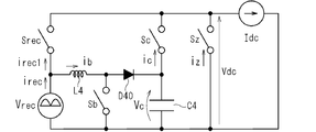
- FIG. 1 is a circuit diagram showing a configuration of a direct power converter 100 to which the control technique described in this embodiment is applied.
- Such a configuration is known in, for example, Non-Patent Document 1 and Patent Documents 1 to 4 described above, and thus detailed description will be omitted.
- the direct power converter 100 includes a rectifier circuit 3, a power buffer circuit 4, an inverter 5, and a DC link 7.
- the DC link 7 has power supply lines LH and LL.
- the rectifier circuit 3 is connected between the single phase AC power supply 1 and the DC link 7.
- the rectifier circuit 3 includes, for example, diodes D31 to D34, which form a diode bridge.
- Power supply line LH is at a higher potential than power supply line LL.
- the rectifier circuit 3 outputs pulsating power (details will be described later) to the DC link 7.
- the rectifier circuit 3 has a filter in the direct current link 7 side is illustrated here.
- the said filter is LC filter provided with the reactor L2 and the capacitor
- the capacitor C2 is connected between the power supply lines LH and LL, and the reactor L2 is connected in series to the power supply line LH on the diode bridge side with respect to the capacitor C2.
- the filter prevents the high frequency component resulting from the switching operation of the inverter 5 from propagating to the single phase AC power supply 1.
- the filter may be omitted. In the following embodiments, since the function of the filter can be ignored, the description will be made by omitting this function.
- the power buffer circuit 4 has a function of buffering a part of the AC component of the pulsating power as buffering power.
- the power buffer circuit 4 includes a capacitor C4, a discharge circuit 4a and a charging circuit 4b, and exchanges power with the DC link 7.
- the capacitor C4 is a buffer capacitor, the discharging circuit 4a discharges the capacitor C4, and the charging circuit 4b charges the capacitor C4.
- the discharge circuit 4a further includes diodes D42 and D43, and a transistor (here, insulated gate bipolar transistor: hereinafter abbreviated as "IGBT") Sc connected in anti-parallel to the diode D42.
- the transistor Sc is connected to the capacitor C4 on the side of the power supply line LH in series with the capacitor C4 between the power supply lines LH and LL. The switching of the transistor Sc is controlled by the control signal SSc.
- the anti-parallel connection means that the forward directions are mutually connected in parallel.
- the forward direction of the transistor Sc is a direction from the power supply line LL to the power supply line LH
- the forward direction of the diode D42 is a direction from the power supply line LH to the power supply line LL.
- the transistor Sc and the diode D42 can be collectively understood as one switch element (switch Sc). The conduction of the switch Sc discharges the capacitor C 4 to apply power to the DC link 7.
- the diode D43 has a function of preventing the discharge of the capacitor C4 from causing the capacitor C2 to be charged.
- the diode D43 is a current blocking element serving as an element for blocking the flow of current from the switch Sc to the rectifier circuit 3 between the switch Sc and the rectifier circuit 3 in the power supply line LH. When the rectifier circuit 3 does not have a filter on the DC link 7 side, the diode D43 can be omitted.
- the charging circuit 4b boosts the rectified voltage Vrec to charge the capacitor C4.
- the charging circuit 4b includes, for example, a diode D40, a reactor L4, and a transistor (here, IGBT) Sb.
- the diode D40 comprises a cathode and an anode, which is connected between the switch Sc and the capacitor C4.
- Such a configuration is known as a so-called boost chopper.
- the switching of the transistor Sb is controlled by the control signal SSb.
- Reactor L4 is connected between power supply line LH and the anode of diode D40.
- the transistor Sb is connected between the power supply line LL and the anode of the diode D40.
- the diode D41 is connected in reverse parallel to the transistor Sb, and both can be collectively regarded as one switch element (switch Sb). Specifically, the forward direction of the transistor Sb is a direction from the power supply line LH to the power supply line LL, and the forward direction of the diode D41 is a direction from the power supply line LL to the power supply line LH.
- the capacitor C4 is charged by the charging circuit 4b, and a voltage (hereinafter referred to as "both-end voltage") Vc higher than the rectified voltage Vrec is generated in the capacitor C4. Specifically, energy is stored in reactor L4 by flowing a current from power supply line LH to power supply line LL via switch Sb, and then the switch Sb is turned off to transmit the energy via diode D40. It is accumulated in the capacitor C4.
- the diode D 42 secures a reverse withstand voltage when the voltage Vc at both ends is lower than the rectified voltage Vrec, and reversely conducts the current flowing back from the inductive load 6 to the DC link 7 when the inverter 5 abnormally stops.
- the diode D41 is a diode for providing reverse withstand voltage and reverse conduction, and the diode D41 itself does not participate in the circuit operation.
- the inverter 5 converts a DC voltage between the power supply lines LH and LL into an AC voltage and outputs it to the output terminals Pu, Pv and Pw.
- the inverter 5 includes six switching elements Sup, Svp, Swp, Sun, Svn and Swn. Switching elements Sup, Svp, Swp are connected between output ends Pu, Pv, Pw and power supply line LH, and switching elements Sun, Svn, Swn are respectively connected between output ends Pu, Pv, Pw and power supply line LL.
- Connected to The inverter 5 constitutes a so-called voltage source inverter, and includes six diodes Dup, Dvp, Dwp, Dun, Dvn, Dwn.
- the diodes Dup, Dvp, Dwp, Dun, Dvn, Dwn are all disposed with their cathodes on the side of the power supply line LH and their anodes on the side of the power supply line LL.
- the diode Dup is connected in parallel with the switching element Sup between the output end Pu and the power supply line LH.
- the diodes Dvp, Dwp, Dun, Dvn, Dwn are connected in parallel with the switching elements Svp, Swp, Sun, Svn, Swn, respectively.
- Load currents iu, iv and iw are outputted from the output terminals Pu, Pv and Pw, respectively, and these constitute three-phase alternating current.
- IGBTs are adopted as the switching elements Sup, Svp, Swp, Sun, Svn, Swn.
- the inverter 5 operates by switching of the switching elements Svp, Swp, Sun, Svn, Swn controlled by the inverter control signal SSg. That is, the inverter 5 is controlled by the inverter control signal SSg.
- the inductive load 6 is, for example, a rotating machine, and is illustrated by an equivalent circuit showing that it is an inductive load.
- the load current iu, iv, iw flowing in the inductive load 6, the single phase AC voltage Vin and the rectified voltage Vrec are measured It is input as a value.
- the input of the rectified voltage Vrec may be omitted.
- the command for the operation of the inductive load 6 is a command value of an average value of the both-ends voltage Vc, which is a command value of the both-ends voltage Vc * which is a command value
- a value is input to the controller 10.
- the command value for the operation is a rotational angular velocity command ⁇ m * which is a command value of the rotational angular velocity ⁇ m of the rotary machine.
- FIG. 2 is a circuit diagram showing an equivalent circuit of direct power converter 100.
- the equivalent circuit itself is also introduced, for example, in Non-Patent Document 1 and Patent Documents 1 to 4.
- the current irec1 is equivalently represented as a current irec1 passing through when the switch Srec conducts.
- the discharge current ic flowing out of the capacitor C4 when the capacitor C4 is discharged is equivalently represented as a current ic passing through when the switch Sc conducts.
- the current flowing to the inductive load 6 via the inverter 5 is equal to that when the switch Sz conducts. It is equivalently expressed as a zero-phase current iz flowing via this.
- FIG. 2 a reactor L4 constituting the charging circuit 4b, a diode D40, and a switch Sb are shown, and a reactor current ib flowing through the reactor L4 is additionally described.
- the duty dr is a duty for setting a period in which the rectifier circuit 3 can flow the current irec1 to the DC link 7, and this is hereinafter referred to as a rectification duty dr.
- the rectification duty dr can be said to be a duty that causes the rectification circuit 3 to conduct with the DC link 7.
- the duty dc is a duty at which the capacitor C4 discharges, and this is hereinafter referred to as a discharge duty dc.
- the duty dz is a duty through which the zero phase current iz always flows regardless of the voltage output from the inverter 5, and this is hereinafter referred to as the zero duty dz.
- the currents irec1, ic, and iz are respectively the products obtained by multiplying the DC link current Idc input from the DC link 7 to the inverter 5 by the duties dr, dc, and dz. Therefore, these are the switching periods of the switches Srec, Sc, and Sz.
- the average value of The duties dr, dc, dz can also be viewed as the current distribution ratio of the link current Idc to the respective currents irec, ic, iz.
- the rectifier circuit 3 can not actively flow the current irec1 to the DC link 7. Therefore, conduction / non-conduction of the switch Srec is controlled by switching the inverter 5 and the switch Sc in accordance with the zero duty dz and the discharge duty dc, respectively, and the current irec1 can be obtained accordingly.
- the inverter 5 can not utilize the DC voltage in the DC link 7 in a period in which the zero-phase current iz flows. Therefore, the DC voltage used to supply power to the inverter 5 in the DC link 7 has meaning in power conversion. In other words, an instantaneous DC voltage which the inverter 5 does not use for power conversion has no meaning when considering the voltage utilization factor.
- a direct current voltage having meaning in power conversion is referred to as a virtual direct current voltage Vdc in this embodiment, and can be expressed as in the following equation (5).
- the virtual DC voltage Vdc is represented by the sum of the product Vrec ⁇ dr of the rectification duty dr and the rectification voltage Vrec and the product Vc ⁇ dc of the discharge duty dc and the voltage Vc at both ends. Ru.
- the virtual DC voltage Vdc can also be understood as the voltage applied to the DC link 7 as an average of the maximum value of the voltage that can be output by the inverter 5 for the cycle for controlling the switching of the switches Sc and Sb and the inverter 5 .
- the inverter 5 can contribute to the voltage of the DC link 7 at a ratio of zero duty dz, the inverter 5 is insulated from any one of the DC links 7 in a period corresponding to the zero duty dz.
- the virtual DC voltage Vdc is added in FIG. 2 as a voltage generated at both ends of the inverter 5 and a current source Idc (which flows the link current Idc) representing the load thereof.
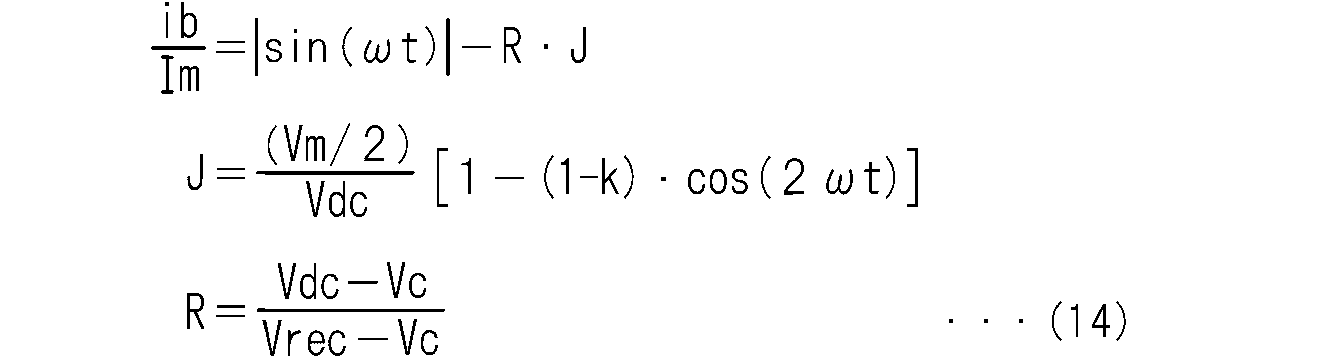
- Equation (6) the instantaneous input power Pin input to the rectifier circuit 3 is expressed by Equation (6), where the input power factor is 1.
- the amplitude Im of the input current Iin, the phase ⁇ t and the amplitude Vm of the single-phase AC voltage Vin are introduced. Since the input power factor is 1, the phase ⁇ t of the single-phase AC voltage Vin is adopted as the phase of the input current Iin.
- the instantaneous input power Pin has an AC component (-1/2) ⁇ Vm ⁇ Im ⁇ cos (2 ⁇ t) indicated by the second term on the right side of the equation (6) (hereinafter, also referred to as “AC component Pin ⁇ ”) . Therefore, the instantaneous input power Pin is also referred to as pulsating power Pin. Since the rectifier circuit 3 does not have the function of storing and branching power, it can be said that the pulsating power Pin is output from the rectifier circuit 3 to the DC link 7.
- the power buffer circuit 4 performs buffering with a buffering power Pbuf obtained by multiplying the AC component Pin ⁇ by a distribution ratio k of 0 or more and 1 or less.
- the inverter 5 receives the power represented by the equation (7) from the DC link 7 and outputs the load currents iu, iv, iw.
- the inverter 5 receives the pulsating power Pin as it is as the input power Pdc from the DC link 7 as it is.
- Pbuf 0, which corresponds to the case where the power buffer circuit 4 does not share power at all.
- Pdc Pin-Pin ⁇ . This corresponds to the case where the power buffer circuit 4 exchanges power corresponding to the absolute value
- the distribution ratio k indicates how much of the absolute value
- the link current Idc is expressed by equation (8) (see, for example, Patent Document 4).
- equation (11) is established using the equation (9). Further, since the waveform of the input current Iin is a sine wave, the output current irec is expressed by equation (12). Further, referring to FIG. 2, the equation (13) is established. Therefore, equation (14) is obtained in consideration of equation (8).
- the first value J and the second value R are introduced in equation (14) for the convenience of the following description.
- the value ib / Im on the left side of the first equation of the equation (14) is a value obtained by normalizing the reactor current ib with the amplitude Im. Since reactor current ib is a current input to charging circuit 4b, value ib / Im is temporarily referred to as a normalized charging current. Further, since it can be said that the absolute value
- , the first value J, and the second value R are sufficient to obtain the normalized charging current ib / Im.
- the first value J is calculated using the virtual DC voltage Vdc, the phase ⁇ t, the amplitude Vm, and the distribution ratio k.
- the second value R is calculated using the virtual DC voltage Vdc, the voltage Vrec, and the both-end voltage Vc. Therefore, when obtaining the normalized charging current ib / Im, detection of the current is unnecessary.
- control signal SSb for controlling switch Sb a command value of reactor current ib is required as described later, and even if a command value of normalized charging current ib / Im is calculated ,
- the amplitude Im of the input current Iin is required.
- the command value of the amplitude Im is set based on the deviation between the both-end voltage Vc and the both-end voltage command Vc *. Therefore, when controlling the operation of the charging circuit 4b, a measured value of the voltage Vc at both ends is required, but detection of the current is not necessary.
- the discharge duty dc for controlling the switch Sc may be a value (1-R), and the detection of the current is not necessary.
- the normalized charging current ib / Im is set to zero.
- the rectification duty dr in this case can be obtained by dividing the normalized current command
- the discharge duty dc is obtained by the equation (16) based on the equation (5) which does not depend on the reactor current ib.
- Equation (19) is obtained by considering the equation (14) in the same way as deriving it from the equations (8) and (9).
- the equation (19) is formally the same as that of the equation (14) in which the value 0 is used instead of the voltage Vc. That is, in equation (19), Vdc / Vrec is adopted as the second value R in equation (14).
- the normalized charging current ib / Im is set to zero.
- the rectification duty dr, the discharge duty dc, and the zero duty dz are expressed by the equations (15), (16), and (17), respectively.
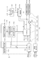
- FIG. 3 is a block diagram illustrating the configuration of the control device 10.
- the control device 10 can realize the above control technology. However, since control is performed so as to set virtual DC voltage Vdc to a desired value, virtual DC voltage command Vdc *, which is the command value as virtual DC voltage Vdc, is calculated in equations (14), (15), and (16). To adopt.
- the control device 10 includes an inverter control unit 101, a normalized current command generation unit 102, a buffer control unit 103, and a voltage command generation unit 108.
- the inverter control unit 101 outputs an inverter control signal SSg based on the rectification duty dr, the discharge duty dc, and the voltage commands Vu *, Vv *, Vw *.
- the voltage commands Vu *, Vv *, Vw are command values of the voltage output from the inverter 5.
- Voltage command generation unit 108 generates and outputs voltage commands Vu *, Vv *, Vw * based on rotational angular velocity command ⁇ m * and load currents iu, iv, iw.
- the functions of the inverter control unit 101 and the voltage command generation unit 108 and the configuration for realizing the same are known, and thus the description thereof is omitted here.
- the normalized current command generation unit 102 generates and outputs a normalized current command
- this is described as the command value of the current normalized with the amplitude Im of the input current Iin.
- itself is a dimensionless number, there is not necessarily a limitation to be used in association with the current value as employed in the equation (15).
- the normalized current command generation unit 102 includes, for example, a power supply phase detector 102 a, a trigonometric function generator 102 b, and an absolute value generator 102 c.
- the power supply phase detector 102a detects and outputs the phase ⁇ t from the single-phase AC voltage Vin.
- the trigonometric function generator 102 b generates and outputs a sine value sin ( ⁇ t) using the phase ⁇ t.
- the absolute value generator 102c calculates an absolute value of the sine value sin ( ⁇ t) to generate and output a normalized current command
- the buffer control unit 103 includes an amplitude setting unit 103a, a charge command generation unit 103b, a charge operation control unit 103c, a discharge operation control unit 103d, a normalized link current estimation unit 103e, and a calculation unit 103f.
- the amplitude setting unit 103a sets an amplitude command Im *, which is a command value of the amplitude Im, based on the deviation between the both-end voltage command Vc * and the both-end voltage Vc.
- the deviation is realized by performing proportional control or proportional integral control.
- the both-end voltage Vc is proportional to the integral value of the current charging the capacitor C4. Therefore, the amplitude setting unit 103a can perform proportional control or substantially perform proportional integral control.
- Charge command generation unit 103b generates charge command ib * which is a command value of reactor current ib. Specifically, charge command generation unit 103b is a multiplier, and generates a charge command ib * by multiplying amplitude command Im * by a normalized charge command that is a command value of normalized charge current ib / Im.
- the normalized charge command is expressed by adopting the symbol “ib * / Im *”. That is, the symbol does not mean division. The symbol only indicates that it is a multiplicand from which the charge command ib * can be obtained by multiplying the amplitude command Im *. The generation of the normalized charge command ib * / Im * will be described later.
- the charging operation control unit 103c controls the charging operation of the charging circuit 4b based on the charging command ib *. Specifically, the charge operation control unit 103c generates a control signal SSb.
- the function of the charging operation control unit 103c and the configuration for realizing the function are known (for example, Patent Document 3), and the details thereof are omitted here.
- the discharge operation control unit 103d discharges the capacitor C4 based on the discharge duty dc. Specifically, the discharge operation control unit 103d generates a control signal SSc.
- the function of the discharge operation control unit 103 d and the configuration for realizing the function are well known, and the details thereof will be omitted here.
- the normalized link current estimation unit 103e estimates a value obtained by normalizing the link current Idc flowing through the DC link 7 with the amplitude Im. In this estimation, the link current Idc is not estimated once and then normalized with the amplitude Im. A value obtained by normalizing the link current Idc with the amplitude Im is estimated.
- this estimate is expressed using the symbol "Idc ⁇ / Im *". That is, the symbol does not mean division. The symbol only indicates that it is a multiplicand from which an estimated value Idc ⁇ of the link current Idc can be obtained by multiplying the amplitude command Im *. However, in the present embodiment, it is not necessary to obtain the estimated value Idc ⁇ itself.
- Such estimated value Idc ⁇ / Im * can be calculated by the equation (20) by assuming the virtual DC voltage command Vdc * as the virtual DC voltage Vdc in the equation (8) and the amplitude command Im * in the amplitude Im. Desired.
- the estimated value Idc ⁇ / Im * is determined by the first value J adopting the virtual DC voltage command Vdc * as the virtual DC voltage Vdc in the equation (14) Be This is because the direct power converter 100 is controlled such that the virtual DC voltage Vdc becomes the virtual DC voltage command Vdc *.
- the normalized link current estimation unit 103e calculates the first value J using the virtual DC voltage command Vdc *, the phase ⁇ t and the amplitude Vm of the single-phase AC voltage Vin, and the distribution ratio k. Is output as an estimated value Idc ⁇ / Im *.
- the normalized link current estimation unit 103 e includes a power supply amplitude detector 103 r and a calculation unit 103 s.
- the power supply amplitude detector 103r receives the single-phase AC voltage Vin, obtains an amplitude Vm, and outputs this.
- the calculator 103s receives the amplitude Vm, the virtual DC voltage command Vdc *, the distribution factor k, and the cosine value cos (2 ⁇ t), calculates a first value J using these, and estimates the first value J as an estimated value Idc ⁇ / Output as Im *.
- the cosine value cos (2 ⁇ t) may be obtained by the calculation unit 103s by obtaining the phase ⁇ t from the power supply phase detector 102a.
- the calculator 103 f generates and outputs the normalized charge command ib * / Im *, the rectification duty dr, and the discharge duty dc.
- Vdc> Vrec when the right side of the first equation of the equation (14) is non-negative, as is understood by comparing the equations (9) and (14), the second value R is used as the rectification duty dr. Output. In addition, a second value R is subtracted from 1 as the discharge duty dc and output.
- Vdc ⁇ Vrec the discharge duty dc is set to 0 and output when the right side of the first equation of Formula (19) is non-negative, and the second value R is output as the rectification duty dr.
- the virtual DC voltage command Vdc * is adopted as the virtual DC voltage Vdc. This is because the direct power converter 100 is controlled such that the virtual DC voltage Vdc becomes the virtual DC voltage command Vdc *.
- the voltage Vc and the rectified voltage Vrec are input to the calculation unit 103f. Although these are all measurement values, the rectified voltage Vrec may be estimated. This is because the rectified voltage Vrec can be estimated as the product of the amplitude Vm and the normalized current command
- the calculation unit 103 f outputs the second value R as the rectification duty dr
- the normalized charge command ib * / Im * is obtained by subtracting the product R ⁇ J from the normalized current command
- the discharge duty dc is outputted by (1-R) in the case of Vdc> Vrec, and is outputted with the value 0 in the case of Vdc ⁇ Vrec.
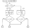
- FIGS. 4 and 5 are flowcharts showing the setting of the rectification duty dr, the discharge duty dc, and the normalized charge command ib * / Im * by the calculation unit 103 f.
- the flowchart shown in FIG. 4 and the flowchart shown in FIG. 5 are connected to each other by connectors Q1, Q2 and Q3.
- step S101 it is determined whether virtual DC voltage Vdc is larger than rectified voltage Vrec. As described above, since the direct power converter 100 is controlled such that the virtual DC voltage Vdc becomes the virtual DC voltage command Vdc *, it is determined whether or not Vdc *> Vrec. Also in the following steps, the virtual DC voltage command Vdc * is adopted as the virtual DC voltage Vdc.
- step S101 determines whether the determination result of step S101 is affirmative, step S102 is executed, and if negative, step S103 is executed.
- step S102 the second value R is calculated and determined in accordance with equation (14) and in step S103 according to equation (19).
- step S104 It is determined in step S104 whether or not the normalized current command
- step S108 Even if the determination result in step S104 is negative, or even if the determination result in step S105 is negative, the rectification duty dr, the discharge duty dc, and the normalized charge command ib * / Im * are set in step S108. . If the normalized current command
- step S106 If the determination result of step S104 is affirmative, the rectification duty dr, the discharge duty dc, and the normalized charge command ib * / Im * are set in step S106. Specifically, the rectification duty dr is set to the second value R by the equations (9) and (14). Further, the normalized charge command ib * / Im * is set using the normalized charge current ib / Im shown in equation (14). The discharge duty dc is set to (1-R) by the equations (10) and (14).
- step S107 If the determination result of step S105 is affirmative, the rectification duty dr, the discharge duty dc, and the normalized charge command ib * / Im * are set in step S107. Specifically, the rectification duty dr is set to the second value R by the equations (18) and (19). Further, the normalized charge command ib * / Im * is set using the normalized charge current ib / Im shown in equation (19). The discharge duty dc is set to 0 as described above.
- control device 10 uses the distribution factor k, the virtual DC voltage command Vdc *, the both-end voltage command Vc *, the single-phase AC voltage Vin, the both-end voltage Vc, and the rectified voltage Vrec.
- the control of the power buffer circuit 4 described in the principle of control of the direct power converter is realized. That is, in control of the power buffer circuit 4, detection of current is unnecessary.
- control device 10 is illustrated as a block diagram, but can be realized by including, for example, a microcomputer and a storage device.
- the microcomputer executes each processing step (in other words, a procedure) described in the program.
- the storage device can be configured by one or more of various storage devices such as ROM (Read Only Memory), RAM (Random Access Memory), and rewritable non-volatile memory (EPROM (Erasable Programmable ROM)). .
- ROM Read Only Memory
- RAM Random Access Memory
- EPROM Erasable Programmable ROM
- the storage device stores various information, data, and the like, stores a program executed by a microcomputer, and provides a work area for executing the program.
- the microcomputer can be understood as functioning as various means corresponding to each processing step described in the program, or it can be understood as realizing various functions corresponding to each processing step.
- the control device 10 may be realized by hardware for some or all of the components illustrated in the block diagram.
- the duty dr, dc, dz in the second stage, the virtual DC voltage Vdc and its first component dr ⁇ Vrec, the second component dc ⁇ Vc and the link current Idc.
- the third stage shows the currents irec, irec, ib, ic, and the fourth stage shows the electric powers Pin, -Pb, Pc, Pbuf, Prec.
- the power Pc indicates the power output from the power buffer circuit 4 to the DC link 7
- the power Pb indicates the power input from the power buffer circuit 4 to the DC link 7, and the relationship of equation (23) is satisfied.
- the horizontal axis is a phase ⁇ t in units of degrees.
- the first component dr ⁇ Vrec of the virtual DC voltage Vdc is a voltage that appears in the first term of the right side of the equation (5), and indicates the contribution of the rectifier circuit 3 to the virtual DC voltage Vdc.
- the second component dc ⁇ Vc of the virtual DC voltage Vdc is a voltage that appears in the second term of the right side of the equation (5), and indicates the contribution of the capacitor C4 to the virtual DC voltage Vdc.
- a period in which Vdc> Vrec is divided into a period F corresponding to the period E in FIG. 6 and dz> 0, ib 0, and a period G other than that.
- the period G corresponds to the period E in FIG. 6 and the time when the phase ⁇ t is 90 degrees and 270 degrees.
- the waveform of the current irec can be a sine wave, and both the virtual DC voltage Vdc and the link current Idc can be made constant. (Refer Formula (8) etc.).
- Vdc ⁇ Vrec A period in which Vdc ⁇ Vrec is shown as a period M in FIG.
- the period L corresponds to the period N in FIG. 8 and the time when the phase ⁇ t is 90 degrees and 270 degrees.
Abstract
直接形電力変換器に用いられる電力バッファ回路の制御において、電流の検出を不要とする。正規化リンク電流推定部(103e)は、仮想直流電圧指令(Vdc*)、単相交流電圧の位相(ωt)及び振幅(Vm)並びに分配率(k)を用いて計算される第1値を、直流リンクからインバータへ流れるリンク電流を正規化した値の推定値(Idc^/Im*)として採用する。計算部(103f)は、仮想直流電圧指令(Vdc*)、整流電圧(Vrec)、両端電圧(Vc)を用いて計算される第2値を求める。正規化電流指令(|sin(ωt)|)が第1値と第2値との積未満であれば、正規化充電指令(ib*/Im*)は0に設定され、整流デューティ(dr)は正規化電流指令(|sin(ωt)|)を第1値で除して求められる。
Description
この発明は、直流リンクを介して相互に接続された整流回路、インバータ、電力バッファ回路を備えた直接形電力変換器を、制御する技術に関する。
単相交流電源から得られる電力には、電源周波数の二倍の周波数の脈動が存在する。従って、単相交流電源から得られる単相交流電圧を整流して直流電圧を得る場合、この直流電圧を一定にするためには大容量のエネルギー蓄積要素が必要となる。
かかる必要性に鑑み、スイッチング素子を介してバッファコンデンサを直流リンクに接続し、これによって電圧源を生成する電力バッファ回路を採用した技術が提案されている(例えば下掲の特許文献1、非特許文献1)。かかる技術によれば、当該電圧源は、単相交流電源から得られる電圧とともに、高周波リンクを生成する直接形電力変換器において入力される電流の波形を正弦波とし、高い効率の特性が実現される。
上記の技術では、単相交流電電圧の波高値まで、直流リンクの直流電圧を高めることができる(例えば非特許文献1)。しかしバッファコンデンサが担うバッファ電圧として、実用的な値、例えば上記波高値の1.17倍の値を選択すると、電圧利用率は0.87程度に留まる。他方、同じバッファ電圧でも電圧利用率を0.95まで改善する制御方式が提案されている(例えば下掲の特許文献2)。
上述の様な、電力バッファ回路との間で授受される電力の大きさに基づく制御方式とは異なり、電力変換器から出力される電圧に着目した制御方式も提案されている(例えば下掲の特許文献3及び非特許文献1)。当該制御方式では、電力バッファ回路が分担する電力(直流リンクとの間で授受される電力)における定常電力の割合を増すことにより昇圧動作を実現する。かかる制御方式では、分担する電力が大幅に増加しない電圧範囲では効果的である。
なお、バッファ電圧に基づいて入力電流の振幅を制御する技術を開示する例として、特許文献4を挙げておく。
山下、榊原、「アクティブバッファ付き単相-三相電力変換器の電圧利用率を改善する電力制御法」、電気学会論文誌D、137巻、2号、電気学会、2017年2月1日、p.112-118
特許文献3に示される制御方式では、電力バッファ回路が分担する電力は、他の要因によって受動的に決定される。具体的には、入力電流を正弦波とするように電力バッファ回路に流す電流を決定することで、電力バッファ回路が分担する電力の大きさが決定される。具体的な構成は示されていないものの、電力バッファ回路に流す電流を上述の様に決定するためには、諸処の電流を検出するための電流検出器が必要であり、制御回路の複雑化を招く。
この発明は上記の事情に鑑みてなされたもので、電力バッファ回路の制御において、電流の検出を不要とする技術を提供することを目的とする。
この発明にかかる直接形電力変換器用制御装置は、直接形電力変換器を制御する制御装置(10)である。ここで、前記直接形電力変換器は、第1電源線(LH)及び第2電源線(LL)を含む直流リンク(7)と、単相交流電圧(Vin)を全波整流し、前記第1電源線を前記第2電源線よりも高電位にして前記直流リンクに脈動電力(Pin)を出力する整流回路(3)と、前記第1電源線と前記第2電源線との間に設けられ、前記脈動電力(Pin)の交流成分(Pin^)に0以上1以下の分配率kを乗じたバッファリング電力(Pbuf)でバッファリングする電力バッファ回路(4)と、前記直流リンクに印加された電圧を交流電圧に変換するインバータ(5)とを備える。そして前記電力バッファ回路は、コンデンサ(C4)と、前記コンデンサを放電する放電回路(4a)と、前記コンデンサを充電する充電回路(4b)とを含む。
前記制御装置は、インバータ制御部(101)と、正規化電流指令生成部(102)と、バッファ制御部(103)とを備える。
前記インバータ制御部(101)は、前記整流回路が前記直流リンクと導通するデューティである整流デューティdrと、前記コンデンサが放電するデューティである放電デューティdcと、前記インバータが出力する電圧の指令値(Vu*,Vv*,Vw*)に基づいて、前記インバータの動作を制御するインバータ制御信号(SSg)を出力する。
前記正規化電流指令生成部(102)は、前記整流回路が出力する出力電流(irec)を、前記整流回路へ入力される入力電流(Iin)の振幅(Im)で正規化した電流の指令値たる正規化電流指令(|sin(ωt)|)を生成して出力する。
前記バッファ制御部(103)は、振幅設定部(103a)と、充電指令生成部(103b)と、充電動作制御部(103c)と、放電動作制御部(103d)と、正規化リンク電流推定部(103e)と、計算部(103f)とを有する。
前記振幅設定部(103a)は、前記コンデンサの両端電圧Vcの平均値についての指令値たる両端電圧指令(Vc*)と前記両端電圧Vcとの偏差に基づいて、前記入力電流の前記振幅(Im)の指令値たる振幅指令(Im*)を設定する。
前記充電指令生成部(103b)は、正規化充電指令(ib*/Im*)を前記振幅指令に乗じて、前記充電回路に流れる電流(ib)の指令値たる充電指令(ib*)を生成する。
前記充電動作制御部(103c)は、前記充電指令に基づいて前記充電回路の充電動作を制御する。前記放電動作制御部(103d)は、前記放電デューティdcに基づいて前記コンデンサを放電させる。
前記正規化リンク電流推定部(103e)は、仮想直流電圧指令Vdc*、前記単相交流電圧の位相ωt及び振幅Vm並びに前記分配率kを用いて計算される第1値(J)を、前記直流リンクから前記インバータへ流れるリンク電流(Idc)を前記入力電流の前記振幅(Im)で正規化した値の推定値(Idc^/Im*)として採用して出力する。
前記仮想直流電圧指令Vdc*は仮想直流電圧(Vdc)の指令値である。前記仮想直流電圧(Vdc)は、dr・Vrec+dc・Vcで表される。
前記計算部(103f)は、前記仮想直流電圧指令Vdc*、前記整流回路が出力する整流電圧Vrec、前記両端電圧Vcを用いて計算される第2値(R)を求める。そして前記計算部(103f)は、前記正規化電流指令(|sin(ωt)|)が、前記第1値と前記第2値との積(R・J)未満であれば、前記正規化電流指令(|sin(ωt)|)を前記第1値(J)で除して求めて前記整流デューティdrとして出力し、前記放電デューティdcを(Vdc*-dr・Vrec)/Vcによって求めて出力し、前記正規化充電指令を0に設定して出力する。
電力バッファ回路の制御において、電流の検出が不要である。
この発明の目的、特徴、局面、および利点は、以下の詳細な説明と添付図面とによって、より明白となる。
A.電力変換器の構成.
図1は、この実施の形態において説明される制御技術が適用される、直接形電力変換器100の構成を示す回路図である。かかる構成は例えば上述の非特許文献1、特許文献1~4で公知であるため、詳細な説明は省略する。
図1は、この実施の形態において説明される制御技術が適用される、直接形電力変換器100の構成を示す回路図である。かかる構成は例えば上述の非特許文献1、特許文献1~4で公知であるため、詳細な説明は省略する。
直接形電力変換器100は、整流回路3と、電力バッファ回路4と、インバータ5と、直流リンク7とを備えている。直流リンク7は電源線LH,LLを有する。
整流回路3は、単相交流電源1と直流リンク7との間に接続されている。整流回路3は例えばダイオードD31~D34を備え、これらがダイオードブリッジを構成する。整流回路3は、単相交流電源1から入力される単相交流電圧Vinを全波整流して整流電圧Vrec(=|Vin|)に変換し、これを電源線LH,LLの間に出力する。つまり整流電圧Vrecは整流回路3が出力する出力電圧である。電源線LHは電源線LLよりも高電位である。整流回路3には単相交流電源1から入力電流Iinが入力され、整流回路3は出力電流irec(=|Iin|)を出力する。整流回路3は直流リンク7に脈動電力(詳細は後述する)を出力する。
なお、ここでは整流回路3が直流リンク7側にフィルタを有している場合が例示される。当該フィルタはリアクトルL2とコンデンサC2とを備えるLCフィルタである。コンデンサC2は電源線LH,LLの間に接続され、リアクトルL2はコンデンサC2よりも上記ダイオードブリッジ側で電源線LHに対して直列に接続されている。当該フィルタは、インバータ5のスイッチング動作に起因する高周波成分が単相交流電源1へ伝搬することを防止する。当該フィルタは省略しても良い。以下の実施の形態では、当該フィルタの機能は無視できるので、この機能を省略した説明を行なう。
電力バッファ回路4は脈動電力の交流成分の一部をバッファリング電力としてバッファリングする機能を有する。電力バッファ回路4はコンデンサC4、放電回路4a及び充電回路4bを有し、直流リンク7との間で電力を授受する。コンデンサC4はバッファコンデンサであり、放電回路4aはコンデンサC4を放電し、充電回路4bはコンデンサC4を充電する。
放電回路4aはダイオードD42,D43と、ダイオードD42に対して逆並列接続されたトランジスタ(ここでは絶縁ゲート型バイポーラトランジスタ:以下「IGBT」と略記)Scを更に含んでいる。トランジスタScはコンデンサC4に対して電源線LH側で、電源線LH,LLの間でコンデンサC4と直列に接続されている。トランジスタScのスイッチングは制御信号SScによって制御される。
ここで逆並列接続とは、順方向が相互に逆となって並列に接続されていることを指す。具体的にはトランジスタScの順方向は電源線LLから電源線LHへと向かう方向であり、ダイオードD42の順方向は電源線LHから電源線LLへと向かう方向である。トランジスタScとダイオードD42とはまとめて一つのスイッチ素子(スイッチSc)として把握することができる。スイッチScの導通によってコンデンサC4が放電して直流リンク7へと電力を授与する。
ダイオードD43はコンデンサC4の放電がコンデンサC2への充電を招来することを防止する機能を担う。ダイオードD43は電源線LHにおいて、スイッチScと整流回路3との間に、スイッチScから整流回路3への電流の流れを阻止する素子たる電流阻止素子である。整流回路3が直流リンク7側にフィルタを有しない場合には、ダイオードD43を省略することができる。
充電回路4bは整流電圧Vrecを昇圧してコンデンサC4を充電する。充電回路4bは例えば、ダイオードD40と、リアクトルL4と、トランジスタ(ここではIGBT)Sbとを含んでいる。ダイオードD40は、カソードと、アノードとを備え、当該カソードはスイッチScとコンデンサC4との間に接続される。かかる構成はいわゆる昇圧チョッパとして知られている。トランジスタSbのスイッチングは制御信号SSbによって制御される。
リアクトルL4は電源線LHとダイオードD40のアノードとの間に接続される。トランジスタSbは電源線LLとダイオードD40のアノードとの間に接続される。トランジスタSbにはダイオードD41が逆並列接続されており、両者をまとめて一つのスイッチ素子(スイッチSb)として把握することができる。具体的にはトランジスタSbの順方向は電源線LHから電源線LLへと向かう方向であり、ダイオードD41の順方向は電源線LLから電源線LHへと向かう方向である。
コンデンサC4は充電回路4bにより充電され、コンデンサC4には整流電圧Vrecよりも高い電圧(以下「両端電圧」と称す)Vcが発生する。具体的には電源線LHからスイッチSbを経由して電源線LLへと電流を流すことによってリアクトルL4にエネルギーを蓄積し、その後にスイッチSbをオフすることによって当該エネルギーがダイオードD40を経由してコンデンサC4に蓄積される。
両端電圧Vcは整流電圧Vrecより高いので、基本的にはダイオードD42には電流が流れない。従ってスイッチScの導通/非導通は専らトランジスタScのそれに依存する。ここで、ダイオードD42は両端電圧Vcが整流電圧Vrecより低い場合の逆耐圧を確保するとともに、インバータ5が異常停止したときに誘導性負荷6から直流リンク7へ還流する電流を逆導通させるように作用する。
また、電源線LHの方が電源線LLよりも電位が高いので、基本的にはダイオードD41には電流が流れない。従ってスイッチSbの導通/非導通は専らトランジスタSbのそれに依存する。ここで、ダイオードD41は逆耐圧や逆導通をもたらすためのダイオードであり、ダイオードD41それ自体は回路動作には関与しない。
インバータ5は電源線LH,LLの間の直流電圧を交流電圧に変換して出力端Pu,Pv,Pwに出力する。インバータ5は6つのスイッチング素子Sup,Svp,Swp,Sun,Svn,Swnを含む。スイッチング素子Sup,Svp,Swpはそれぞれ出力端Pu,Pv,Pwと電源線LHとの間に接続され、スイッチング素子Sun,Svn,Swnはそれぞれ出力端Pu,Pv,Pwと電源線LLとの間に接続される。インバータ5はいわゆる電圧形インバータを構成し、6つのダイオードDup,Dvp,Dwp,Dun,Dvn,Dwnを含む。
ダイオードDup,Dvp,Dwp,Dun,Dvn,Dwnはいずれもそのカソードを電源線LH側に、そのアノードを電源線LL側に向けて配置される。ダイオードDupは、出力端Puと電源線LHとの間で、スイッチング素子Supと並列に接続される。同様にして、ダイオードDvp,Dwp,Dun,Dvn,Dwnは、それぞれスイッチング素子Svp,Swp,Sun,Svn,Swnと並列に接続される。出力端Pu,Pv,Pwからは、それぞれ負荷電流iu,iv,iwが出力され、これらは三相交流電流を構成する。例えばスイッチング素子Sup,Svp,Swp,Sun,Svn,SwnにはIGBTが採用される。インバータ5はインバータ制御信号SSgで制御されるスイッチング素子Svp,Swp,Sun,Svn,Swnのスイッチングによって動作する。つまりインバータ5はインバータ制御信号SSgによって制御される。
誘導性負荷6は例えば回転機であり、誘導性負荷であることを示す等価回路で図示されている。
直接形電力変換器用制御装置(図面及び以下では単に「制御装置」と表現する)10には、誘導性負荷6に流れる負荷電流iu,iv,iw、単相交流電圧Vin、整流電圧Vrecが測定値として入力される。但し後述するように、整流電圧Vrecの入力を省略してもよい。また、両端電圧Vcの平均値の指令値たる両端電圧指令Vc*、後述する分配率k、後述する仮想直流電圧Vdcの指令値たる仮想直流電圧指令Vdc*、誘導性負荷6の動作についての指令値が制御装置10に入力される。誘導性負荷6として回転機を採用した場合には、当該動作についての指令値は、当該回転機の回転角速度ωmの指令値たる回転角速度指令ωm*である。
図2は、直接形電力変換器100の等価回路を示す回路図である。当該等価回路それ自体も、例えば非特許文献1、特許文献1~4で紹介されている。当該等価回路において電流irec1は、スイッチSrecが導通するときにこれを経由する電流irec1として等価的に表されている。同様に、コンデンサC4の放電時にコンデンサC4から流れ出る放電電流icは、スイッチScが導通するときにこれを経由する電流icとして等価的に表されている。
但しスイッチSrecの導通は、整流回路3が直流リンク7と導通することを示す。スイッチScが導通すれば、整流電圧Vrecよりも高い両端電圧Vcが直流リンク7に印加されるので、電流irec1は流れず、スイッチSrecは導通しない。
インバータ5において出力端Pu,Pv,Pwが電源線LH,LLのいずれか一方に共通して接続されるときにインバータ5を介して誘導性負荷6に流れる電流は、スイッチSzが導通するときにこれを経由して流れる零相電流izとして等価的に表されている。
また図2では、充電回路4bを構成するリアクトルL4とダイオードD40とスイッチSbとが表され、リアクトルL4を流れるリアクトル電流ibが付記されている。
このようにして得られた等価回路において、スイッチSrec,Sc,Szが導通するそれぞれのデューティdr,dc,dzを導入する。但し、上述の文献から公知のように、下式(1)~(4)が成立する。
デューティdrは整流回路3が直流リンク7に電流irec1を流し得る期間を設定するデューティであり、以降これを整流デューティdrと称す。整流デューティdrは整流回路3が直流リンク7と導通するデューティであると言える。
デューティdcは、コンデンサC4が放電するデューティであり、以降これを放電デューティdcと称す。
デューティdzはインバータ5においてその出力する電圧によらずに必ず零相電流izが流れるデューティであり、以降これを零デューティdzと称す。
電流irec1,ic,izはそれぞれ、直流リンク7からインバータ5に入力される直流のリンク電流Idcにデューティdr,dc,dzを乗算したものであるので、これらはスイッチSrec,Sc,Szのスイッチング周期における平均値である。またデューティdr,dc,dzは、各電流irec1,ic,izに対するリンク電流Idcの電流分配率と見ることもできる。
整流回路3は、能動的に直流リンク7に電流irec1を流すことはできない。よって零デューティdzと、放電デューティdcとに従って、それぞれインバータ5と、スイッチScがスイッチングすることによって、スイッチSrecの導通/非導通が制御され、これに応じて電流irec1を得ることができる。
インバータ5は零相電流izが流れる期間においては、直流リンク7における直流電圧を利用することができない。よって、直流リンク7においてインバータ5への電力供給に利用される直流電圧が電力変換において意味を持つ。換言すれば瞬時的な直流電圧であってインバータ5が電力変換に用いないものは、電圧利用率を考察するに際しても意味を有しない。電力変換において意味を持つ直流電圧をこの実施の形態において仮想直流電圧Vdcと称し、下式(5)のように、表現できる。右辺第3項は0であるので、仮想直流電圧Vdcは、整流デューティdrと整流電圧Vrecとの積Vrec・drと、放電デューティdcと両端電圧Vcとの積Vc・dcとの和で表される。
仮想直流電圧Vdcはまた、インバータ5が出力できる電圧の最大値の、スイッチSc,Sbやインバータ5のスイッチングを制御する周期についての平均として、直流リンク7に印加される電圧と把握することもできる。インバータ5は零デューティdzという比率で直流リンク7の電圧に寄与し得るものの、零デューティdzに対応する期間においてはインバータ5は直流リンク7のいずれか一方と絶縁されているからである。
仮想直流電圧Vdcは、図2において、インバータ5及びその負荷を表す電流源Idc(これはリンク電流Idcを流す)の両端に生じる電圧として付記した。
B.直接形電力変換器の制御の原理.
特許文献4で教示されるように、整流回路3に入力される瞬時入力電力Pinは、入力力率を1として、式(6)で表される。ここで、入力電流Iinの振幅Im、単相交流電圧Vinの位相ωt及び振幅Vmを導入した。入力力率を1としたので、入力電流Iinの位相にも単相交流電圧Vinの位相ωtを採用した。
特許文献4で教示されるように、整流回路3に入力される瞬時入力電力Pinは、入力力率を1として、式(6)で表される。ここで、入力電流Iinの振幅Im、単相交流電圧Vinの位相ωt及び振幅Vmを導入した。入力力率を1としたので、入力電流Iinの位相にも単相交流電圧Vinの位相ωtを採用した。
瞬時入力電力Pinは、式(6)の右辺の第2項で示される交流成分(-1/2)・Vm・Im・cos(2ωt)を有する(以下、「交流成分Pin^」とも称す)。よって瞬時入力電力Pinを脈動電力Pinとも称する。整流回路3は電力を蓄積、分岐させる機能を有しないので、脈動電力Pinは整流回路3から直流リンク7へ出力される、と言うこともできる。
電力バッファ回路4は、交流成分Pin^に0以上1以下の分配率kを乗じたバッファリング電力Pbufでバッファリングする。これにより、インバータ5は直流リンク7から、式(7)で示される電力を入力し、負荷電流iu,iv,iwを出力する。

つまりk=0であればインバータ5は直流リンク7から入力電力Pdcとして脈動電力Pinがそのまま入力される。これはPbuf=0を意味し、電力バッファ回路4は電力を全く分担しない場合に相当する。k=1であればPdc=Pin-Pin^となる。これは電力バッファ回路4が、交流成分Pin^の絶対値|Pin^|に相当する電力を直流リンク7との間で授受している場合に相当する。
つまり分配率kは、交流成分Pin^の絶対値|Pin^|のどの程度が、バッファリング電力Pbufとして電力バッファ回路4に分配されるかを示している。
このような分配率kを導入することにより、リンク電流Idcが式(8)で表される(例えば特許文献4を参照)。

(b-1)仮想直流電圧Vdcが整流電圧Vrecより大きい場合.
分配率kに拘らず式(5)は成立する。よって仮想直流電圧Vdcを増大させるためには、インバータ5の電力変換に寄与しない期間を小さくすることが望ましい。よってまず式(3)に基づいて、dz=0が成立可能な場合を想定する。これが成立しない場合については後述する。このとき式(4)、(5)から、整流デューティdr、放電デューティdcは、それぞれ式(9),(10)となる。Vc>Vdc>Vrecの関係があるので、0<dr<1,0<dc<1である。
分配率kに拘らず式(5)は成立する。よって仮想直流電圧Vdcを増大させるためには、インバータ5の電力変換に寄与しない期間を小さくすることが望ましい。よってまず式(3)に基づいて、dz=0が成立可能な場合を想定する。これが成立しない場合については後述する。このとき式(4)、(5)から、整流デューティdr、放電デューティdcは、それぞれ式(9),(10)となる。Vc>Vdc>Vrecの関係があるので、0<dr<1,0<dc<1である。


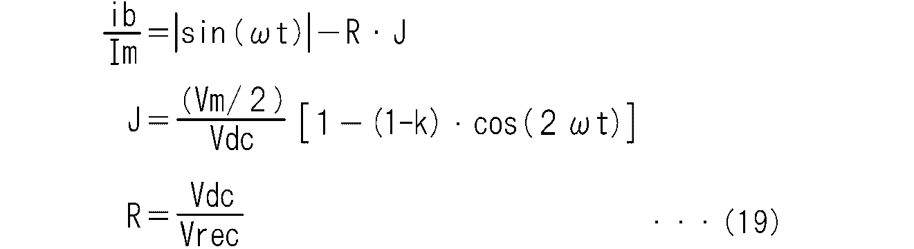
整流デューティdrは、リンク電流Idcに対する電流irec1の比であるので、式(9)を用いて式(11)が成立する。また、入力電流Iinの波形は正弦波であるので、出力電流irecは式(12)で表される。また、図2を参照して式(13)が成立する。よって式(8)をも考慮して式(14)が得られる。後の説明の便宜のため,式(14)において第1値J、第2値Rを導入した。

式(14)の第1式の左辺の値ib/Imは、リアクトル電流ibを振幅Imで正規化した値である。リアクトル電流ibは充電回路4bに入力される電流であるので、値ib/Imを正規化充電電流と仮称する。また、絶対値|sin(ωt)|は、整流回路3が出力する電流irecを振幅Imで正規化した電流の指令値と言えるので、これを正規化電流指令と仮称する。
式(14)から判るように、正規化充電電流ib/Imを求めるに際して、正規化電流指令|sin(ωt)|と、第1値Jと、第2値Rとで足りる。第1値Jは、仮想直流電圧Vdc、位相ωt、振幅Vm、分配率kを用いて計算される。第2値Rは仮想直流電圧Vdc、電圧Vrec、両端電圧Vcを用いて計算される。よって正規化充電電流ib/Imを求めるに際し、電流の検出が不要である。
なるほど、スイッチSbを制御するための制御信号SSbを得るためには、後述するように、リアクトル電流ibの指令値が必要であり、正規化充電電流ib/Imの指令値が計算されてもなお、入力電流Iinの振幅Imが必要である。しかしながら振幅Imを測定する必要はない。例えば特許文献3,4で説明されるように、振幅Imの指令値が、両端電圧Vcと両端電圧指令Vc*との偏差に基づいて設定されるからである。よって充電回路4bの動作を制御する場合には、両端電圧Vcの測定値が要求されるが、電流の検出は必要ではない。
もちろん、式(10)から理解されるように、スイッチScを制御するための放電デューティdcは値(1-R)とすればよく、電流の検出は必要ではない。
次に、dz=0とならない場合について説明する。これはdz=0として計算される電流irec1=Idc-icが大きくなった結果、これを出力電流irecで賄えない場合に相当する。これは換言すれば、式(14)の第1式の右辺が負となってしまう場合である。しかし実際にはリアクトル電流ibは非負であるので、正規化充電電流ib/Imを式(14)で求めるべきではない。
よってリアクトル電流ibを流さず(ib=0)、電流irec1を出力電流irecで全て賄えるように、整流デューティdr、放電デューティdcを設定する。これにより零デューティdzを不必要に増大させることが回避できる。もちろん、この場合には正規化充電電流ib/Imを0とする。
式(14)において正規化充電電流ib/Imを0とし、式(9)を考慮して式(14)において第2値Rを整流デューティdrに置換することにより、式(15)で整流デューティdrが求められる。

つまりこの場合の整流デューティdrは、正規化電流指令|sin(ωt)|を第1値Jで除して求められる。位相ωtが|sin(ωt)|=0を満足する値をとるとき、dr=0である。つまりリアクトル電流ibを流す場合とは異なり、リアクトル電流ibを流さない場合においては整流デューティdrは値0をとり得る。
このとき放電デューティdcは、リアクトル電流ibに依存しない式(5)に基づいて、式(16)で求められる。

このとき零デューティdzは、式(4),(15),(16)から式(17)で表される。
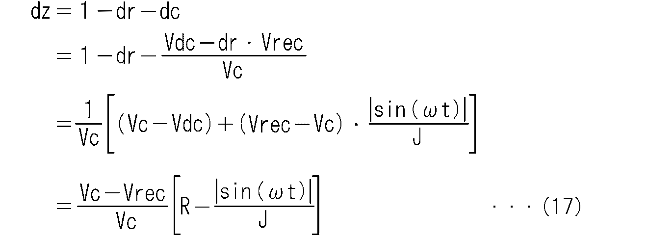
よって式(14)の第1式の右辺が負となる状況では、整流デューティdrと放電デューティdcとをそれぞれ式(15),(16)に設定することにより、零デューティdzは正の値となる(つまりdz=0にはならない)。
(b-2)仮想直流電圧Vdcが整流電圧Vrec以下の場合.
この場合、式(5)に鑑みれば、電圧の観点ではdc=0とできる。更にリアクトル電流ibを流す場合には、irec1=dr・Idcであるので、整流デューティdrは出力電流irecによる制限を受けない。よってこのような場合、整流デューティdrは電圧の観点のみで決定され、式(18)で決定される。またdc=0であったので、式(4)からdz=1-drとなる。Vdc=Vrecのとき、dr=1,dz=0である。
この場合、式(5)に鑑みれば、電圧の観点ではdc=0とできる。更にリアクトル電流ibを流す場合には、irec1=dr・Idcであるので、整流デューティdrは出力電流irecによる制限を受けない。よってこのような場合、整流デューティdrは電圧の観点のみで決定され、式(18)で決定される。またdc=0であったので、式(4)からdz=1-drとなる。Vdc=Vrecのとき、dr=1,dz=0である。

上記式(14)を式(8),(9)から導出したのと同様に考えて、式(19)が得られる。式(19)は、式(14)において両端電圧Vcの代わりに値0を用いたものと形式的に同一である。つまり式(19)は式(14)において第2値RとしてVdc/Vrecを採用したことになる。
次に、dc=0とならない場合について説明する。これはdc=0として計算される電流irec1を出力電流irecで賄えない場合に相当する。これは換言すれば、式(19)の第1式の右辺が負となってしまう場合である。しかし実際にはリアクトル電流ibは非負であるので、正規化充電電流ib/Imを式(19)で求めるべきではない。
よってリアクトル電流ibを流さず(ib=0)、電流irec1を出力電流irecで全て賄えるように、整流デューティdr、放電デューティdcを設定する。もちろん、この場合には正規化充電電流ib/Imを0とする。
従って、この場合においても、式(15),(16),(17)でそれぞれ整流デューティdr、放電デューティdc、零デューティdzが表される。
以上のようにして、本実施の形態にかかる制御技術では、電力バッファ回路4の制御において、電流の検出が不要である。
C.制御装置10の構成例.
図3は制御装置10の構成を例示するブロック図である。制御装置10によって上記の制御技術が実現できる。但し、仮想直流電圧Vdcを所望の値にすべく制御を行うので、式(14),(15),(16)の計算においては、仮想直流電圧Vdcとしてその指令値たる仮想直流電圧指令Vdc*を採用する。
図3は制御装置10の構成を例示するブロック図である。制御装置10によって上記の制御技術が実現できる。但し、仮想直流電圧Vdcを所望の値にすべく制御を行うので、式(14),(15),(16)の計算においては、仮想直流電圧Vdcとしてその指令値たる仮想直流電圧指令Vdc*を採用する。
制御装置10は、インバータ制御部101と、正規化電流指令生成部102と、バッファ制御部103と、電圧指令生成部108を備える。
インバータ制御部101は、整流デューティdrと、放電デューティdcと、電圧指令Vu*,Vv*,Vw*とに基づいて、インバータ制御信号SSgを出力する。電圧指令Vu*,Vv*,Vwはインバータ5が出力する電圧の指令値である。電圧指令生成部108は、回転角速度指令ωm*、負荷電流iu,iv,iwに基づいて電圧指令Vu*,Vv*,Vw*を生成して出力する。インバータ制御部101及び電圧指令生成部108の機能及びそれを実現するための構成は公知であるので、ここでの説明は省略する。
正規化電流指令生成部102は正規化電流指令|sin(ωt)|を生成して出力する。式(12)を用いて正規化電流指令|sin(ωt)|に言及した際、これは出力電流irecを、入力電流Iinの振幅Imで正規化した電流の指令値であると説明した。しかしながら正規化電流指令|sin(ωt)|の値それ自体は無次元数であるので、式(15)で採用されるように、必ずしも電流値と関連づけて用いる制限はない。
正規化電流指令生成部102は例えば電源位相検出器102a、三角関数生成器102b、絶対値生成器102cを有する。電源位相検出器102aは、単相交流電圧Vinからその位相ωtを検出して出力する。三角関数生成器102bは位相ωtを用いて正弦値sin(ωt)を生成して出力する。絶対値生成器102cは正弦値sin(ωt)の絶対値を計算して正規化電流指令|sin(ωt)|を生成して出力する。
バッファ制御部103は、振幅設定部103aと、充電指令生成部103bと、充電動作制御部103cと、放電動作制御部103dと、正規化リンク電流推定部103eと、計算部103fとを有する。
振幅設定部103aは、両端電圧指令Vc*と両端電圧Vcとの偏差に基づいて、振幅Imの指令値たる振幅指令Im*を設定する。当該偏差から振幅指令Im*を生成するには、当該偏差に対して比例制御、あるいは比例積分制御を行なって実現される。なお、両端電圧VcはコンデンサC4を充電する電流の積分値に比例する。よって振幅設定部103aは比例制御を行なうということもできるし、実質的には比例積分制御を行なうということもできる。
充電指令生成部103bは、リアクトル電流ibの指令値たる充電指令ib*を生成する。充電指令生成部103bは、具体的には乗算器であって、正規化充電電流ib/Imの指令値たる正規化充電指令を、振幅指令Im*に乗じて、充電指令ib*を生成する。
かかる演算に鑑み、便宜上、正規化充電指令は記号「ib*/Im*」を採用して表現する。つまり当該記号は除算を意味しない。当該記号は、振幅指令Im*を乗じることによって充電指令ib*が得られる被乗数であることを示すに過ぎない。正規化充電指令ib*/Im*の生成については後述する。
充電動作制御部103cは、充電指令ib*に基づいて、充電回路4bの充電動作を制御する。具体的には充電動作制御部103cは、制御信号SSbを生成する。かかる充電動作制御部103cの機能及びこれを実現するための構成は公知であり(例えば特許文献3)、ここではその詳細を省略する。
放電動作制御部103dは、放電デューティdcに基づいてコンデンサC4を放電させる。具体的には放電動作制御部103dは、制御信号SScを生成する。かかる放電動作制御部103dの機能及びこれを実現するための構成は公知であり、ここではその詳細を省略する。
正規化リンク電流推定部103eは、直流リンク7に流れるリンク電流Idcを振幅Imで正規化した値を推定する。この推定においては、リンク電流Idcを一旦推定してから振幅Imで正規化するのではない。リンク電流Idcを振幅Imで正規化した値を推定する。
便宜上、この推定値は記号「Idc^/Im*」を採用して表現する。つまり当該記号は除算を意味しない。当該記号は、振幅指令Im*を乗じたならば、リンク電流Idcの推定値Idc^たる値が得られる被乗数であることを示すに過ぎない。但し本実施の形態においては推定値Idc^自体を求める必要がない。
このような推定値Idc^/Im*は、式(8)において仮想直流電圧Vdcとして仮想直流電圧指令Vdc*を、振幅Imに振幅指令Im*を、それぞれ想定することによって、式(20)で求められる。

式(14),(20)を比較して判るように、推定値Idc^/Im*は、式(14)において仮想直流電圧Vdcとして仮想直流電圧指令Vdc*を採用した第1値Jで求められる。仮想直流電圧Vdcが仮想直流電圧指令Vdc*となるように、直接形電力変換器100が制御されるからである。
換言すれば、正規化リンク電流推定部103eは、第1値Jを、仮想直流電圧指令Vdc*、単相交流電圧Vinの位相ωt及び振幅Vm並びに分配率kを用いて計算して求め、これを推定値Idc^/Im*として採用して出力する。
正規化リンク電流推定部103eは、電源振幅検出器103rと、計算部103sとを有する。電源振幅検出器103rは単相交流電圧Vinを入力し、振幅Vmを得てこれを出力する。計算部103sは振幅Vm、仮想直流電圧指令Vdc*、分配率k、余弦値cos(2ωt)を入力し、これらを用いて第1値Jを計算し、第1値Jを推定値Idc^/Im*として出力する。
図3では、余弦値cos(2ωt)は三角関数生成器102bによって生成される場合が例示される。但し、余弦値cos(2ωt)は、電源位相検出器102aから位相ωtを得て、計算部103sが求めてもよい。
計算部103fは正規化充電指令ib*/Im*、整流デューティdr、放電デューティdcを生成して出力する。Vdc>Vrecの場合には、式(14)の第1式の右辺が非負のとき、式(9),(14)を比較して理解されるように、整流デューティdrとして第2値Rを出力する。また放電デューティdcとして1から第2値Rを減じて出力する。Vdc≦Vrecの場合には、式(19)の第1式の右辺が非負のとき、放電デューティdcを0に設定して出力し、整流デューティdrとして第2値Rを出力する。
但し、第2値Rを式(14)(Vdc>Vrecのとき)あるいは式(19)(Vdc≦Vrecのとき)によって計算するに際し、仮想直流電圧Vdcとして仮想直流電圧指令Vdc*を採用する。仮想直流電圧Vdcが仮想直流電圧指令Vdc*となるように、直接形電力変換器100が制御されるからである。
正規化充電指令ib*/Im*は、式(14)あるいは式(19)においていずれもVdc=Vdc*とした第1値J及び第2値R、正規化電流指令|sin(ωt)|で計算される。かかる計算を行なう必要性から、計算部103fには、絶対値生成器102cから正規化電流指令|sin(ωt)|が、正規化リンク電流推定部103eから推定値Idc^/Im*として第1値Jが、それぞれ入力される。計算部103fは仮想直流電圧指令Vdc*、整流電圧Vrec、両端電圧Vcを用いて第2値Rを計算して求める。
第2値Rを計算する必要性から、計算部103fには両端電圧Vc、整流電圧Vrecが入力される。これらはいずれも測定値であるが、整流電圧Vrecは推定値を計算してもよい。整流電圧Vrecは振幅Vmと正規化電流指令|sin(ωt)|との積として推定できるからである。よって整流電圧Vrecの入力に替えて、電源振幅検出器103rから振幅Vmを得て(図3の破線矢印参照)、計算部103fはその内部において整流電圧Vrecを推定してもよい。
従って計算部103fは、正規化電流指令|sin(ωt)|が、第1値Jと第2値Rとの積R・J以上であれば、整流デューティdrとして第2値Rを出力し、正規化充電指令ib*/Im*を正規化電流指令|sin(ωt)|から積R・Jを減じて求めて出力する。但し、放電デューティdcについては、Vdc>Vrecの場合には(1-R)によって出力し、Vdc≦Vrecの場合には値0で出力する。
同様にして、正規化電流指令|sin(ωt)|が、積R・J未満であれば、式(15),(16)において仮想直流電圧Vdcとして仮想直流電圧指令Vdc*を想定し、正規化電流指令|sin(ωt)|を第1値Jで除して求めて整流デューティdrとして出力し、放電デューティdcを(Vdc*-dr・Vrec)/Vcによって出力し、正規化充電指令ib*/Im*を0に設定して出力する。このとき、仮想直流電圧指令Vdc*と整流電圧Vrecとの大小関係は不問である。
図4および図5は、計算部103fによる整流デューティdr、放電デューティdc、正規化充電指令ib*/Im*の、上述の設定を示すフローチャートである。図4に示されたフローチャートと図5に示されたフローチャートとは、結合子Q1,Q2,Q3によって互いに結合する。
ステップS101では、仮想直流電圧Vdcが整流電圧Vrecよりも大きいか否かが判断される。上述の様に、仮想直流電圧Vdcが仮想直流電圧指令Vdc*となるように直接形電力変換器100が制御されるので、Vdc*>Vrecであるか否かが判断される。以下のステップでも、仮想直流電圧Vdcとして仮想直流電圧指令Vdc*が採用される。
ステップS101の判断結果が肯定的であればステップS102が実行され、否定的であればステップS103が実行される。ステップS102では式(14)に従って、ステップS103では式(19)に従って、それぞれ第2値Rが計算して求められる。
ステップS102によって求められた第2値Rを用いて、正規化電流指令|sin(ωt)|が積R・J以上であるか否かが、ステップS104において判断される。ステップS103によって求められた第2値Rを用いて、正規化電流指令|sin(ωt)|が積R・J以上であるか否かが、ステップS105において判断される。
ステップS104の判断結果が否定的であっても、ステップS105の判断結果が否定的であっても、ステップS108において整流デューティdr、放電デューティdc、正規化充電指令ib*/Im*が設定される。正規化電流指令|sin(ωt)|が積R・J未満であれば、整流デューティdr、放電デューティdcがそれぞれ式(15),(16)によって設定される。またリアクトル電流ibを流さず、正規化充電指令ib*/Im*を0に設定する。
ステップS104の判断結果が肯定的であれば、ステップS106において整流デューティdr、放電デューティdc、正規化充電指令ib*/Im*が設定される。具体的には整流デューティdrは式(9),(14)によって第2値Rに設定される。また、正規化充電指令ib*/Im*は式(14)に示された正規化充電電流ib/Imを用いて設定される。放電デューティdcは式(10),(14)によって(1-R)に設定される。
ステップS105の判断結果が肯定的であれば、ステップS107において整流デューティdr、放電デューティdc、正規化充電指令ib*/Im*が設定される。具体的には整流デューティdrは式(18),(19)によって第2値Rに設定される。また、正規化充電指令ib*/Im*は式(19)に示された正規化充電電流ib/Imを用いて設定される。放電デューティdcは上述のように0に設定される。
ステップS106,S107,S108のいずれかが実行されると、整流デューティdr、放電デューティdc、正規化充電指令ib*/Im*の設定は終了する。このようにして設定された整流デューティdr、放電デューティdc、正規化充電指令ib*/Im*は計算部103fから出力される。
以上のように、制御装置10は、分配率k、仮想直流電圧指令Vdc*、両端電圧指令Vc*、及び単相交流電圧Vin、両端電圧Vc、整流電圧Vrecを用いて、上述の「B.直接形電力変換器の制御の原理.」で説明された電力バッファ回路4の制御を実現する。つまり電力バッファ回路4の制御において、電流の検出が不要である。
なお、上記の説明では制御装置10の構成をブロック図で例示したが、例えばマイクロコンピュータと記憶装置を含んで構成して実現できる。マイクロコンピュータは、プログラムに記述された各処理ステップ(換言すれば手順)を実行する。上記記憶装置は、例えばROM(Read Only Memory)、RAM(Random Access Memory)、書き換え可能な不揮発性メモリ(EPROM(Erasable Programmable ROM)等)などの各種記憶装置の一つ又は複数で構成可能である。当該記憶装置は、各種の情報やデータ等を格納し、またマイクロコンピュータが実行するプログラムを格納し、また、プログラムを実行するための作業領域を提供する。なお、マイクロコンピュータは、プログラムに記述された各処理ステップに対応する各種手段として機能するとも把握でき、あるいは、各処理ステップに対応する各種機能を実現するとも把握できる。もちろん、制御装置10は、ブロック図で例示された各構成要素の一部又は全部をハードウェアで実現されても構わない。
D.実施例.
以下、上記の制御技術について、種々の場合についての実施例を示す。
以下、上記の制御技術について、種々の場合についての実施例を示す。
(d-1)k=1の場合.
この場合、電力バッファ回路4は絶対値|Pin^|に相当する電力を直流リンク7との間で授受する。そして式(14)では第1値Jが(Vm/2)/Vdcとなり、制御装置10において推定値Idc^/Im*は(Vm/2)/Vdc*で計算される。
この場合、電力バッファ回路4は絶対値|Pin^|に相当する電力を直流リンク7との間で授受する。そして式(14)では第1値Jが(Vm/2)/Vdcとなり、制御装置10において推定値Idc^/Im*は(Vm/2)/Vdc*で計算される。
よって正規化電流指令|sin(ωt)|が積R・J(但し第2値Rの計算にはVdc=Vdc*を採用する)以上である場合には、各値は式(21)で表され、積R・J未満である場合には、各値は式(22)で表される。

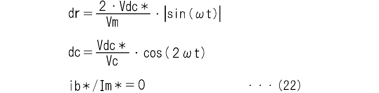
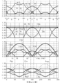
図6は、k=1であって、仮想直流電圧指令Vdc*を振幅Vmに等しく設定したときの直接形電力変換器100の諸量の波形を示すグラフである。よって位相ωtが90度、270度となる時点においてはVdc=Vrec(上記(b-2)参照)であり、それ以外ではVdc>Vrec(上記(b-1)参照)である。
図6において、第1段目にはデューティdr,dc,dzを、第2段目には仮想直流電圧Vdcならびにその第1成分dr・Vrec及び第2成分dc・Vcとリンク電流Idcを、第3段目には電流irec,irec1,ib,icを、第4段目には電力Pin,-Pb,Pc,Pbuf,Precを、それぞれ示す。ここで電力Pcは電力バッファ回路4から直流リンク7へ出力する電力を、電力Pbは電力バッファ回路4が直流リンク7から入力される電力を、それぞれ示し、式(23)の関係がある。いずれのグラフも横軸には「度」を単位とする位相ωtを採用している。

仮想直流電圧Vdcの第1成分dr・Vrecは式(5)の右辺の第1項に現れる電圧であり、仮想直流電圧Vdcに対する整流回路3の寄与分を示す。仮想直流電圧Vdcの第2成分dc・Vcは式(5)の右辺の第2項に現れる電圧であり、仮想直流電圧Vdcに対するコンデンサC4の寄与分を示す。
図6及び後述する図7~図9では、電圧については振幅Vmで正規化し(つまりVm=1とし)、電流については振幅Imを√2として換算して示した。また、両端電圧指令Vc*は振幅Vmの1.17倍に設定した(例えば特許文献2参照)。
位相ωtの値が0,180,360(度)近傍の期間Eでは、式(21)の第3式の右辺の第1項が小さく、よってdz>0,ib=0であり、式(15)~(17)の関係が成立する。期間E以外ではdz=0,ib>0であり、式(9),(10),(14)の関係が成立する。なお、Vdc=Vrecとなる位相ωtが90度、270度となる時点ではdc=0であり、式(18)、(19)が成立する。
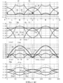
図7はk=1であって、仮想直流電圧指令Vdc*を振幅Vmの√3/2(≒0.87)倍に設定したときのグラフである。よって位相ωtが60~120度、240~300度となる期間(境界を含む)においてはVdc≦Vrec(上記(b-2)参照)であり、それ以外ではVdc>Vrec(上記(b-1)参照)である。
Vdc≦Vrecである期間は図7において期間Hとして示された。Vdc>Vrecとなる期間は、図6における期間Eに相当してdz>0,ib=0となる期間Fと、それ以外の期間Gとに区分される。期間Gは、図6において期間Eと、位相ωtが90度、270度となる時点とを除く期間に相当する。
よって期間Fにおいて式(15)~(17)の関係が成立し、期間Gにおいて式(9),(10),(14)の関係が成立し、期間Hにおいてdc=0、式(18)、(19)が成立する。
図6に示された場合も、図7に示された場合も、k=1であるので、電流irecの波形を正弦波とし、かつ仮想直流電圧Vdc、リンク電流Idcのいずれも一定値にできる(式(8)等参照)。
(d-2)k=1/4の場合.
図8は、k=1/4であって、仮想直流電圧指令Vdc*を振幅Vmに等しく設定したときの直接形電力変換器の諸量の波形を示すグラフである。諸量は図6と同様にして示した。また両端電圧指令Vc*は振幅Vmの1.17倍に設定した。
図8は、k=1/4であって、仮想直流電圧指令Vdc*を振幅Vmに等しく設定したときの直接形電力変換器の諸量の波形を示すグラフである。諸量は図6と同様にして示した。また両端電圧指令Vc*は振幅Vmの1.17倍に設定した。
位相ωtの値が0,180,360(度)近傍の期間Nでは、式(21)の第3式の右辺の第1項が小さく、よってdz>0,ib=0であり、式(15)~(17)の関係が成立する。期間N以外ではdz=0,ib>0であり、式(9),(10),(14)の関係が成立する。なお、Vdc=Vrecとなる位相ωtが90度、270度となる時点ではdc=0であり、式(18),(19)の関係が成立する。
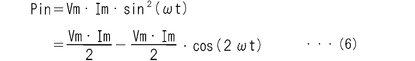
図9はk=1/4であって、仮想直流電圧指令Vdc*を振幅Vmの√3/2(≒0.87)倍に設定したときのグラフである。よって位相ωtが60~120度、240~300度となる期間(境界を含む)においてはVdc≦Vrec(上記(b-2)参照)であり、それ以外ではVdc>Vrec(上記(b-1)参照)である。
Vdc≦Vrecである期間は図9において期間Mとして示された。Vdc>Vrecとなる期間は、図8における期間Nに相当してdz>0,ib=0となる期間Kと、それ以外の期間Lとに区分される。期間Lは、図8において期間Nと、位相ωtが90度、270度となる時点とを除く期間に相当する。
よって期間Kにおいて式(15)~(17)の関係が成立し、期間Lにおいて式(9),(10),(14)の関係が成立し、期間Mにおいてdc=0、式(18)、(19)が成立する。
図8に示された場合も、図9に示された場合も、k=1の場合(図6参照)とは異なり、リンク電流Idcは脈動するが、電流irecの波形を正弦波とし、かつ仮想直流電圧Vdcは一定値にできる。
特許請求の範囲の趣旨及び範囲から逸脱することなく、形態や詳細の多様な変更が可能なことが理解されるであろう。上述の各種の実施形態および変形例は相互に組み合わせることができる。
この発明は詳細に説明されたが、上記した説明は、すべての局面において、例示であって、この発明がそれに限定されるものではない。例示されていない無数の変形例が、この発明の範囲から外れることなく想定され得るものと解される。
Claims (7)
- 直接形電力変換器を制御する制御装置(10)であって、
前記直接形電力変換器は、
第1電源線(LH)及び第2電源線(LL)を含む直流リンク(7)と、
単相交流電圧(Vin)を全波整流し、前記第1電源線を前記第2電源線よりも高電位にして前記直流リンクに脈動電力(Pin)を出力する整流回路(3)と、
前記第1電源線と前記第2電源線との間に設けられ、前記脈動電力(Pin)の交流成分(Pin^)に0以上1以下の分配率kを乗じたバッファリング電力(Pbuf)でバッファリングする電力バッファ回路(4)と、
前記直流リンクに印加された電圧を交流電圧に変換するインバータ(5)と
を備え、
前記電力バッファ回路は、
コンデンサ(C4)と、
前記コンデンサを放電する放電回路(4a)と、
前記コンデンサを充電する充電回路(4b)と
を含み、
前記制御装置は、
インバータ制御部(101)と、
正規化電流指令生成部(102)と、
バッファ制御部(103)と
を備え、
前記インバータ制御部(101)は、前記整流回路が前記直流リンクと導通するデューティである整流デューティdrと、前記コンデンサが放電するデューティである放電デューティdcと、前記インバータが出力する電圧の指令値(Vu*,Vv*,Vw*)に基づいて、前記インバータの動作を制御するインバータ制御信号(SSg)を出力し、
前記正規化電流指令生成部(102)は、前記整流回路が出力する出力電流(irec)を、前記整流回路に入力される入力電流(Iin)の振幅(Im)で正規化した電流の指令値たる正規化電流指令(|sin(ωt)|)を生成して出力し、
前記バッファ制御部(103)は、
前記コンデンサの両端電圧Vcの平均値についての指令値たる両端電圧指令(Vc*)と前記両端電圧Vcとの偏差に基づいて、前記入力電流の前記振幅(Im)の指令値たる振幅指令(Im*)を設定する振幅設定部(103a)と、
正規化充電指令(ib*/Im*)を前記振幅指令に乗じて、前記充電回路に流れる電流(ib)の指令値たる充電指令(ib*)を生成する充電指令生成部(103b)と、
前記充電指令に基づいて前記充電回路の充電動作を制御する充電動作制御部(103c)と、
前記放電デューティdcに基づいて前記コンデンサを放電させる放電動作制御部(103d)と、
仮想直流電圧指令Vdc*、前記単相交流電圧の位相ωt及び振幅Vm並びに前記分配率kを用いて計算される第1値(J)を、前記直流リンクから前記インバータへ流れるリンク電流(Idc)を前記入力電流の前記振幅(Im)で正規化した値の推定値(Idc^/Im*)として採用して出力する、正規化リンク電流推定部(103e)と、
前記仮想直流電圧指令Vdc*、前記整流回路が出力する整流電圧Vrec、前記両端電圧Vcを用いて計算される第2値(R)を求め、前記正規化電流指令(|sin(ωt)|)が、前記第1値と前記第2値との積(R・J)未満であれば、前記正規化電流指令(|sin(ωt)|)を前記第1値(J)で除して求めて前記整流デューティdrとして出力し、前記放電デューティdcを(Vdc*-dr・Vrec)/Vcによって求めて出力し、前記正規化充電指令を0に設定して出力する計算部(103f)と
を有し、
前記仮想直流電圧指令Vdc*は、dr・Vrec+dc・Vcで表される仮想直流電圧(Vdc)の指令値である、直接形電力変換器用制御装置。 - 前記正規化リンク電流推定部(103e)は、前記第1値(J)を((Vm/2)/Vdc*)・(1-(1-k)・cos(2ωt))によって求める、請求項1記載の直接形電力変換器用制御装置。
- 前記正規化電流指令(|sin(ωt)|)が前記積(R・J)以上であれば前記計算部(103f)は、前記整流デューティdrとして前記第2値(R)を出力し、前記正規化充電指令(ib*/Im*)として前記正規化電流指令(|sin(ωt)|)から前記積を減じて出力する、請求項1又は請求項2記載の直接形電力変換器用制御装置。
- 前記仮想直流電圧指令Vdc*が前記整流電圧Vrecよりも大きいときに前記計算部(103f)は、
前記第2値(R)を(Vdc*-Vc)/(Vrec-Vc)によって求め、
前記正規化電流指令(|sin(ωt)|)が、前記積(R・J)以上であれば、前記放電デューティdcとして1から前記第2値(R)を減じて出力する、請求項1乃至請求項3のいずれか一つに記載の直接形電力変換器用制御装置。 - 前記仮想直流電圧指令Vdc*が前記整流電圧Vrec以下のときに前記計算部(103f)は、
前記第2値(R)をVdc*/Vrecによって求め、
前記正規化電流指令(|sin(ωt)|)が、前記積(R・J)以上であれば、前記放電デューティdcを0に設定して出力する、請求項1乃至請求項4のいずれか一つに記載の直接形電力変換器用制御装置。 - 前記計算部(103f)において、前記整流電圧Vrecは前記振幅Vmと前記正規化電流指令との積(Vm・|sin(ωt)|)で推定される、請求項1乃至請求項5のいずれか一つに記載の直接形電力変換器用制御装置。
- 前記整流回路(3)は前記直流リンク(7)側にフィルタ(L2,C2)を有し、
前記放電回路(4a)は、
前記第1電源線と前記第2電源線との間で前記コンデンサ(C4)と直列に、かつ前記コンデンサよりも前記第1電源線側に設けられたスイッチ(Sc,D42)と、
前記第1電源線(LH)において前記スイッチと前記整流回路(3)との間に、前記スイッチから前記整流回路への電流の流れを阻止する電流阻止素子(D43)と
を更に有する、請求項1乃至請求項6のいずれか一つに記載の直接形電力変換器用制御装置。
Priority Applications (2)
| Application Number | Priority Date | Filing Date | Title |
|---|---|---|---|
| US16/620,730 US10666143B2 (en) | 2017-06-30 | 2018-06-28 | Control device for direct power converter |
| EP18824341.4A EP3648332B1 (en) | 2017-06-30 | 2018-06-28 | Direct power converter control device |
Applications Claiming Priority (2)
| Application Number | Priority Date | Filing Date | Title |
|---|---|---|---|
| JP2017-128715 | 2017-06-30 | ||
| JP2017128715A JP6418287B1 (ja) | 2017-06-30 | 2017-06-30 | 直接形電力変換器用制御装置 |
Publications (1)
| Publication Number | Publication Date |
|---|---|
| WO2019004354A1 true WO2019004354A1 (ja) | 2019-01-03 |
Family
ID=64098665
Family Applications (1)
| Application Number | Title | Priority Date | Filing Date |
|---|---|---|---|
| PCT/JP2018/024578 WO2019004354A1 (ja) | 2017-06-30 | 2018-06-28 | 直接形電力変換器用制御装置 |
Country Status (4)
| Country | Link |
|---|---|
| US (1) | US10666143B2 (ja) |
| EP (1) | EP3648332B1 (ja) |
| JP (1) | JP6418287B1 (ja) |
| WO (1) | WO2019004354A1 (ja) |
Families Citing this family (5)
| Publication number | Priority date | Publication date | Assignee | Title |
|---|---|---|---|---|
| CN109739107B (zh) * | 2018-12-18 | 2022-03-18 | 西北工业大学 | 一种基于模型预测控制的功率缓冲器设计方法 |
| JP7161110B2 (ja) * | 2019-03-14 | 2022-10-26 | ダイキン工業株式会社 | 直接形電力変換器用の制御装置 |
| JP7436783B2 (ja) * | 2019-09-30 | 2024-02-22 | ダイキン工業株式会社 | 電力変換装置 |
| JP7212904B2 (ja) * | 2020-08-19 | 2023-01-26 | 矢崎総業株式会社 | 充電器 |
| JP7130024B2 (ja) * | 2020-11-12 | 2022-09-02 | 三菱電機株式会社 | 電力変換装置 |
Citations (6)
| Publication number | Priority date | Publication date | Assignee | Title |
|---|---|---|---|---|
| JPS5626435B2 (ja) | 1977-03-15 | 1981-06-18 | ||
| JPS584167B2 (ja) | 1974-08-06 | 1983-01-25 | ヤマハハツドウキ カブシキガイシヤ | クランクシツヨアツシユクシキ 2 サイクルエンジン |
| JPS5930108B2 (ja) | 1977-01-21 | 1984-07-25 | 日本ゼオン株式会社 | 抗凝血性を有する医療用成形体 |
| JP2011193678A (ja) * | 2010-03-16 | 2011-09-29 | Nagaoka Univ Of Technology | 単相/三相直接変換装置及びその制御方法 |
| JP2014107935A (ja) * | 2012-11-27 | 2014-06-09 | Daikin Ind Ltd | 直接形電力変換装置の制御方法 |
| JP5874800B1 (ja) | 2014-10-15 | 2016-03-02 | ダイキン工業株式会社 | 直接型電力変換器用制御装置 |
Family Cites Families (9)
| Publication number | Priority date | Publication date | Assignee | Title |
|---|---|---|---|---|
| JP2006074965A (ja) * | 2004-09-06 | 2006-03-16 | Honda Motor Co Ltd | 電源装置 |
| JP2011167011A (ja) * | 2010-02-12 | 2011-08-25 | Toyota Central R&D Labs Inc | Dcdcコンバータシステム |
| US9490722B2 (en) * | 2012-09-21 | 2016-11-08 | Daikin Industries, Ltd. | Method of controlling direct power converter |
| US9698699B2 (en) * | 2012-09-27 | 2017-07-04 | Daikin Industries, Ltd. | Direct AC power conversion device |
| JP5804167B2 (ja) | 2013-09-19 | 2015-11-04 | ダイキン工業株式会社 | 電力変換装置 |
| EP3171502B1 (en) * | 2014-07-18 | 2021-01-20 | Daikin Industries, Ltd. | Direct-type ac power conversion device |
| JP5930108B2 (ja) | 2014-09-25 | 2016-06-08 | ダイキン工業株式会社 | 電力変換装置 |
| JP5920520B1 (ja) * | 2014-12-17 | 2016-05-18 | ダイキン工業株式会社 | 充放電回路、充放電回路の制御方法、充放電回路の制御装置、及び直接形電力変換器 |
| JP6265297B1 (ja) * | 2016-09-30 | 2018-01-24 | ダイキン工業株式会社 | 直接形電力変換器用の制御装置 |
-
2017
- 2017-06-30 JP JP2017128715A patent/JP6418287B1/ja active Active
-
2018
- 2018-06-28 US US16/620,730 patent/US10666143B2/en active Active
- 2018-06-28 EP EP18824341.4A patent/EP3648332B1/en active Active
- 2018-06-28 WO PCT/JP2018/024578 patent/WO2019004354A1/ja active Application Filing
Patent Citations (6)
| Publication number | Priority date | Publication date | Assignee | Title |
|---|---|---|---|---|
| JPS584167B2 (ja) | 1974-08-06 | 1983-01-25 | ヤマハハツドウキ カブシキガイシヤ | クランクシツヨアツシユクシキ 2 サイクルエンジン |
| JPS5930108B2 (ja) | 1977-01-21 | 1984-07-25 | 日本ゼオン株式会社 | 抗凝血性を有する医療用成形体 |
| JPS5626435B2 (ja) | 1977-03-15 | 1981-06-18 | ||
| JP2011193678A (ja) * | 2010-03-16 | 2011-09-29 | Nagaoka Univ Of Technology | 単相/三相直接変換装置及びその制御方法 |
| JP2014107935A (ja) * | 2012-11-27 | 2014-06-09 | Daikin Ind Ltd | 直接形電力変換装置の制御方法 |
| JP5874800B1 (ja) | 2014-10-15 | 2016-03-02 | ダイキン工業株式会社 | 直接型電力変換器用制御装置 |
Non-Patent Citations (2)
| Title |
|---|
| See also references of EP3648332A4 |
| YAMASHITASAKAKIBARA: "IEEJ Transactions on Industry Applications", vol. 137, 1 February 2017, THE INSTITUTE OF ELECTRICAL ENGINEERS OF JAPAN, article "A Control Method of a Single-phase-to-three-phase Power Converter with an Active Buffer for Increasing Voltage Transfer Ratio", pages: 112 - 118 |
Also Published As
| Publication number | Publication date |
|---|---|
| JP6418287B1 (ja) | 2018-11-07 |
| EP3648332A4 (en) | 2021-02-17 |
| EP3648332B1 (en) | 2023-05-10 |
| JP2019013093A (ja) | 2019-01-24 |
| EP3648332A1 (en) | 2020-05-06 |
| US10666143B2 (en) | 2020-05-26 |
| US20200106359A1 (en) | 2020-04-02 |
Similar Documents
| Publication | Publication Date | Title |
|---|---|---|
| JP6418287B1 (ja) | 直接形電力変換器用制御装置 | |
| JP6026049B2 (ja) | 電力変換装置 | |
| EP3048718B1 (en) | Power conversion device | |
| EP3051684B1 (en) | Control method for direct power conversion device | |
| EP3200337B1 (en) | Power conversion device | |
| EP3057223B1 (en) | Control method for direct power conversion device | |
| JP6103031B1 (ja) | 電力変換装置の制御装置 | |
| JP5994603B2 (ja) | 直接形電力変換装置の制御方法 | |
| JP6094665B1 (ja) | 電力変換装置の制御装置 | |
| JP5950970B2 (ja) | 電力変換装置 | |
| JP2020167778A (ja) | 直接形電力変換器用の制御装置 | |
| JP6113248B1 (ja) | 電力変換装置 | |
| WO2020184538A1 (ja) | 直接形電力変換器用の制御装置 | |
| WO2021240658A1 (ja) | 電力変換装置、モータ駆動装置、送風機、圧縮機及び空気調和機 | |
| JP2017050921A (ja) | 電源装置及びその充電制御方法 |
Legal Events
| Date | Code | Title | Description |
|---|---|---|---|
| 121 | Ep: the epo has been informed by wipo that ep was designated in this application |
Ref document number: 18824341 Country of ref document: EP Kind code of ref document: A1 |
|
| NENP | Non-entry into the national phase |
Ref country code: DE |
|
| WWE | Wipo information: entry into national phase |
Ref document number: 2018824341 Country of ref document: EP |
|
| ENP | Entry into the national phase |
Ref document number: 2018824341 Country of ref document: EP Effective date: 20200130 |