WO2019003534A1 - 蒸着マスク - Google Patents
蒸着マスク Download PDFInfo
- Publication number
- WO2019003534A1 WO2019003534A1 PCT/JP2018/013198 JP2018013198W WO2019003534A1 WO 2019003534 A1 WO2019003534 A1 WO 2019003534A1 JP 2018013198 W JP2018013198 W JP 2018013198W WO 2019003534 A1 WO2019003534 A1 WO 2019003534A1
- Authority
- WO
- WIPO (PCT)
- Prior art keywords
- opening
- openings
- deposition mask
- metal film
- mask according
- Prior art date
- Legal status (The legal status is an assumption and is not a legal conclusion. Google has not performed a legal analysis and makes no representation as to the accuracy of the status listed.)
- Ceased
Links
Images


Classifications
-
- C—CHEMISTRY; METALLURGY
- C23—COATING METALLIC MATERIAL; COATING MATERIAL WITH METALLIC MATERIAL; CHEMICAL SURFACE TREATMENT; DIFFUSION TREATMENT OF METALLIC MATERIAL; COATING BY VACUUM EVAPORATION, BY SPUTTERING, BY ION IMPLANTATION OR BY CHEMICAL VAPOUR DEPOSITION, IN GENERAL; INHIBITING CORROSION OF METALLIC MATERIAL OR INCRUSTATION IN GENERAL
- C23C—COATING METALLIC MATERIAL; COATING MATERIAL WITH METALLIC MATERIAL; SURFACE TREATMENT OF METALLIC MATERIAL BY DIFFUSION INTO THE SURFACE, BY CHEMICAL CONVERSION OR SUBSTITUTION; COATING BY VACUUM EVAPORATION, BY SPUTTERING, BY ION IMPLANTATION OR BY CHEMICAL VAPOUR DEPOSITION, IN GENERAL
- C23C14/00—Coating by vacuum evaporation, by sputtering or by ion implantation of the coating forming material
- C23C14/04—Coating on selected surface areas, e.g. using masks
- C23C14/042—Coating on selected surface areas, e.g. using masks using masks
-
- H—ELECTRICITY
- H05—ELECTRIC TECHNIQUES NOT OTHERWISE PROVIDED FOR
- H05B—ELECTRIC HEATING; ELECTRIC LIGHT SOURCES NOT OTHERWISE PROVIDED FOR; CIRCUIT ARRANGEMENTS FOR ELECTRIC LIGHT SOURCES, IN GENERAL
- H05B33/00—Electroluminescent light sources
- H05B33/10—Apparatus or processes specially adapted to the manufacture of electroluminescent light sources
-
- H—ELECTRICITY
- H10—SEMICONDUCTOR DEVICES; ELECTRIC SOLID-STATE DEVICES NOT OTHERWISE PROVIDED FOR
- H10K—ORGANIC ELECTRIC SOLID-STATE DEVICES
- H10K71/00—Manufacture or treatment specially adapted for the organic devices covered by this subclass
- H10K71/10—Deposition of organic active material
- H10K71/16—Deposition of organic active material using physical vapour deposition [PVD], e.g. vacuum deposition or sputtering
- H10K71/166—Deposition of organic active material using physical vapour deposition [PVD], e.g. vacuum deposition or sputtering using selective deposition, e.g. using a mask
Definitions
- the present invention relates to a vapor deposition mask.
- the present invention relates to a deposition mask provided with a plurality of openings in a metal film formed by electroforming.
- organic EL display device In the manufacturing process of a display device (hereinafter referred to as "organic EL display device") using an organic EL (electroluminescence) material, a vapor deposition method is used as a technique for forming a thin film composed of the organic EL material. There is. In the case of forming a thin film made of an organic EL material using a vapor deposition method, a vapor deposition mask (also called a metal mask) made of a metal film having a plurality of minute openings is used.
- a vapor deposition mask also called a metal mask
- the organic EL material is selectively selected for a plurality of pixels. Can be deposited.
- the deposition mask can be manufactured by etching a metal plate or can be manufactured using electroforming.
- a deposition mask manufactured using electroforming is suitable for forming a thin film with high accuracy because it is excellent in dimensional accuracy. Therefore, for example, in Patent Document 1, a vapor deposition mask using electroforming is used for vapor deposition of the organic EL material constituting the light emitting layer and the like of the organic EL display device.
- alignment marks are formed on both the deposition mask and the array substrate. For example, in the deposition mask, an opening is formed as an alignment mark, and in the array substrate, an alignment mark having the same shape as the deposition mask is formed. Then, alignment between the deposition mask and the array substrate is performed by matching the contour of the opening of the deposition mask with the contour of the alignment mark of the array substrate.
- an opening is formed as an alignment mark in a deposition mask manufactured using electroforming, but since the deposition mask manufactured using electroforming is made of a metal film, it is extremely thin. Therefore, stress may concentrate in the vicinity of the opening formed as an alignment mark, and the metal film may be warped.
- Alignment between the alignment mark of the deposition mask and the alignment mark of the array substrate is performed using an autofocus mechanism of a camera. At this time, if the vicinity of the alignment mark is warped, focusing by the autofocus mechanism becomes difficult, and there is a problem that alignment using the alignment mark can not be performed.
- the present invention has been made in view of the above problems, and an object of the present invention is to relieve stress generated in the vicinity of an alignment mark disposed on a metal film constituting a deposition mask.
- the deposition mask according to an embodiment of the present invention includes a frame and a metal film held by the frame, and the metal film includes a first opening and a plurality of metal films disposed around the first opening.
- the diameter of the second opening is smaller than the diameter of the first opening.
- FIG. 1 is a plan view showing the configuration of the vapor deposition mask 100 according to the first embodiment.
- the vapor deposition mask 100 includes a frame 102 made of a metal member such as invar, and a plurality of metal films 104 held in a plurality of openings 102 a provided in the frame 102.
- the plurality of metal films 104 are disposed corresponding to the respective organic EL display devices, and function as masks that block the vapor deposition material.
- the metal film 104 is a metal film produced using electroforming, and can be produced, for example, by a plating technique using a metal material such as nickel, nickel-cobalt alloy, iron-nickel alloy, copper or the like.
- the thickness of the metal film may be, for example, in the range of 5 to 20 ⁇ m.
- the metal film 104 has a mask region 104a.
- the mask area 104 a is an area corresponding to the display area of the organic EL display device to be vapor-deposited.
- the mask area 104 a has a plurality of pixel openings at positions corresponding to the respective pixels arranged in the display area of the organic EL display device.
- the plurality of pixel openings are openings for depositing an organic EL material selectively for each pixel.
- FIG. 2 shows a state in which a part inside the mask area 104a (area surrounded by the frame line 106) is enlarged.
- FIG. 2 is a plan view enlarging a part of the inside of the mask region 104 a in the vapor deposition mask 100 according to the first embodiment.
- the metal film 104 is provided with a plurality of pixel openings 107 in a region surrounded by the frame line 106.
- the pixel openings 107 are provided corresponding to the positions of the individual pixels (pixels of the organic EL display device). Note that the metal film 104 shown in FIG. 2 has a pixel opening 107 corresponding to the position of the sub-pixel that emits red, green or blue light. When corresponding to a sub-pixel emitting light of another color, the position of the pixel opening 107 is shifted by one or two columns.
- an alignment mark is disposed in a region of the metal film 104 outside the mask region 104 a.
- the alignment mark is a mark for aligning the deposition mask 100 with a mother glass (not shown) on which a plurality of organic EL display devices are formed.
- FIG. 3 shows a state in which a part of the outside of the mask area 104a (the area surrounded by the frame line 108) is enlarged.
- FIG. 3 is an enlarged plan view of a part of the outside of the mask region 104 a in the vapor deposition mask 100 according to the first embodiment.
- the metal film 104 is provided with the first opening 110 in the region surrounded by the frame 108.
- the first opening 110 is an opening that functions as an alignment mark.
- the present invention is not limited to this, and may be a polygon, a rectangle, an ellipse, or the like. However, in order to minimize the stress generated at the edge of the first opening 110, it is desirable that the outline of the first opening 110 be circular.
- the plurality of second openings 112 and the third openings 114 are disposed around the first opening 110.
- the plurality of second openings 112 and the plurality of third openings 114 are annularly arranged along the contour of the first opening 110.
- the plurality of third openings 114 are disposed outside the second opening 112 with respect to the first opening 110. At this time, as shown in FIG. 3, the plurality of second openings 112 and the plurality of third openings 114 are alternately arranged clockwise or counterclockwise along the outline of the first opening 110. Ru.
- Each of the plurality of second openings 112 and the third openings 114 is an opening functioning as a stress relieving part that relieves stress generated around the first opening 110.
- the arrangement of the plurality of second openings 112 and the third openings 114 is annular, but for example, the outline of the first opening 110 is If it is rectangular, the plurality of second openings 112 and third openings 114 may be disposed along the rectangle. However, this is an example, and it is also possible to arrange the plurality of second openings 112 and the plurality of third openings 114 so as not to follow the contour of the first opening 110.
- FIG. 4 is an enlarged plan view of a part of the first opening 110, the plurality of second openings 112, and the plurality of third openings 114 in the vapor deposition mask 100 according to the first embodiment.
- the diameter of the first opening 110 is R1
- the diameter of the second opening 112 is R2
- the diameter of the third opening 114 is R3, R2 and R3 are smaller than R1.
- R 2 and R 3 preferably have a diameter equal to or less than half of R 1.
- R1 can be 0.5 mm or more and 1.5 mm or less (preferably 0.8 mm or more and 1.2 mm or less), and R2 and R3 can be 150 ⁇ m or more and 250 ⁇ m or less (preferably 180 ⁇ m or more and 220 ⁇ m or less).
- R1 is 1.0 mm, and R2 and R3 are 200 ⁇ m.
- R2 and R3 have the same length, the present invention is not limited to this. R2 and R3 may have different lengths.
- the expression “diameter” is used to indicate their size. It is only an example of an indicator indicating the size.
- the expression “maximum width” is used as an index indicating the size of each opening.
- the “maximum width” is the maximum width (maximum distance) when two points on the contour of the opening are connected by a straight line. That is, when the first opening 110, the second opening 112 and the third opening 114 are circular, the maximum width is equal to the diameter.
- first opening 110, the second opening 112, and the third opening 114 are figures such as a rectangle, a polygon, or an ellipse, in which the distance from the center to the outline changes.
- a relative comparison is possible if the maximum width is used as a measure of
- the plurality of second openings 112 are disposed apart from the edge of the first opening 110 by a predetermined distance L1.
- the autofocusing mechanism uses the plurality of second openings 112 and the plurality of third openings 114 arranged around the first opening 110 as the first opening 110. It is provided to prevent false recognition.
- the predetermined distance L1 is preferably a distance (in the present embodiment, 1.0 mm or more) or more of the diameter (ie, the maximum width) of the first opening 110, but it is particularly preferable if the above-mentioned erroneous recognition can be avoided. There is no limit.
- P1 is 300 ⁇ m or more It may be set in the range of 500 ⁇ m or less (preferably 350 ⁇ m or more and 450 ⁇ m or less). Further, the distance between adjacent ones of the plurality of third openings 114 may be set in the same range.
- the metal film 104 is provided with the first opening 110 as an alignment mark.
- a plurality of second openings 112 and a plurality of third openings 114 having a diameter smaller than that of the first opening 110 are provided so as to surround the periphery of the first opening 110, and the vicinity of the first opening 110 is provided. Relieve stress that occurs in
- the stress generated in the metal film 104 is accumulated as it approaches the first opening 110 from the vicinity of the boundary between the frame 102 and the metal film 104 in FIG.
- the diameter of the first opening 110 is 0.5 mm or more, the problem of warpage is significant.
- the present embodiment by providing the plurality of second openings 112 and the plurality of third openings 114 around the first opening 110 as shown in FIG.
- the stress gradually accumulated from the boundary is relieved in the region where the plurality of second openings 112 and the plurality of third openings 114 are disposed, and does not transmit to the edge of the first opening 110. That is, the bending in the direction perpendicular to the metal film 104 is eliminated, and the problem that the edge of the first opening 110 is warped does not occur. Therefore, according to the present embodiment, accurate alignment using the first opening 110 as an alignment mark is possible.
- the present embodiment is effective when the diameter of the first opening 110 is 0.5 mm or more.
- the plurality of second openings 112 and the plurality of third openings 114 surround the periphery of the first opening 110, and the plurality of second openings 112 and the plurality of third openings Preferably, the openings 114 are staggered, clockwise or counterclockwise, along the contour of the first opening 110.
- the path through which stress is transmitted toward the first opening 110 can be efficiently closed by the plurality of second openings 112 and the plurality of third openings 114, so that stress can be further relieved. It is because the effect is enhanced.
- Second Embodiment In the second embodiment, an example will be described in which the shape of the opening formed in the metal film 104 is different from that of the first embodiment.
- description will be made focusing on the difference in configuration from the vapor deposition mask 100 of the first embodiment, and the same configuration may be assigned the same reference numerals and descriptions thereof may be omitted.
- FIG. 5 is an enlarged plan view of the vicinity of the first opening 110 functioning as an alignment mark in the second embodiment.
- a plurality of second openings 112a and a plurality of third openings 114a having a shape along an arc are arranged around the first opening 110.
- the plurality of third openings 114 a are disposed at positions corresponding to the gaps between the adjacent second openings 112 a. That is, the third opening 114 a is disposed at a position overlapping the gap between the adjacent second openings 112 a when viewed from the first opening 110.
- the metal film 104 of the present embodiment has a configuration in which the stress transmission path toward the first opening 110 is closed by the second opening 112 a and the third opening 114 a.
- the stress gradually accumulated from the boundary between the frame 102 and the metal film 104 is reset in the region where the second opening 112 a and the third opening 114 a are disposed, and the first opening It does not transmit to the edge of the part 110. Therefore, since the problem that the edge of the first opening 110 is bent does not occur, accurate alignment using the first opening 110 as an alignment mark is possible.
- FIG. 6 is an enlarged plan view of the vicinity of the first opening 110 functioning as an alignment mark in the third embodiment.
- the outline of the first opening 110 a is rectangular, and a plurality of second openings 112 b and a plurality of third openings 114 b are disposed along each side around the first opening 110.
- the plurality of second openings 112 b include a plurality of rod-shaped openings.
- the second opening 112 b and the third opening 114 b are rectangular or L-shaped, but may be square.
- the third opening 114 b is disposed at a position corresponding to the gap between the adjacent second openings 112 b. That is, the third opening 114 b is disposed at a position overlapping the gap between the adjacent second openings 112 b when viewed from the first opening 110 a.
- the metal film 104 of the present embodiment has a configuration in which the stress transmission path toward the first opening 110 a is blocked by the second opening 112 b and the third opening 114 b.
- the stress gradually accumulated from the boundary between the frame 102 and the metal film 104 is reset in the region where the second opening 112 b and the third opening 114 b are disposed, and the first opening It does not transmit to the edge of the part 110a. Therefore, since the problem that the edge of the first opening 110a is bent does not occur, accurate alignment using the first opening 110a as an alignment mark is possible.
- vapor deposition mask 102 frame 102a: opening 104: metal film 104a: mask area 107: pixel opening 110, 110a: first opening 112, 112a, 112b: second opening , 114, 114a, 114b ... third opening
Landscapes
- Chemical & Material Sciences (AREA)
- Engineering & Computer Science (AREA)
- Chemical Kinetics & Catalysis (AREA)
- Materials Engineering (AREA)
- Mechanical Engineering (AREA)
- Metallurgy (AREA)
- Organic Chemistry (AREA)
- Manufacturing & Machinery (AREA)
- Electroluminescent Light Sources (AREA)
- Physical Vapour Deposition (AREA)
Abstract
蒸着マスクは、フレームと、前記フレームに保持された金属膜と、を含み、前記金属膜は、第1開口部と、前記第1開口部の周囲に配置された複数の第2開口部を有し、前記第2開口部の最大幅は、前記第1開口部の最大幅よりも小さい。前記複数の第2開口部は、前記第1開口部の輪郭に沿って配置される。第1開口部の輪郭は、円形であってもよい。
Description
本発明は、蒸着マスクに関する。特に、電鋳(Electroforming)で形成された金属膜に複数の開口部を備えた蒸着マスクに関する。
従来、有機EL(エレクトロルミネセンス)材料を用いた表示装置(以下「有機EL表示装置」という。)の製造プロセスにおいては、有機EL材料で構成される薄膜の形成技術として蒸着法が用いられている。蒸着法を用いて有機EL材料で構成される薄膜を形成する場合、複数の微細な開口部を有する金属膜で構成された蒸着マスク(メタルマスクとも呼ばれる。)を用いる。具体的には、複数の画素(すなわち、有機EL材料を蒸着する領域)に対応して複数の開口部が形成された蒸着マスクを用いることにより、複数の画素に対して選択的に有機EL材料を蒸着することができる。
蒸着マスクは、金属板をエッチングして作製したり電鋳を用いて作製したりすることができる。特に、電鋳を用いて作製した蒸着マスクは、寸法精度に優れるため、高精度な薄膜形成には適している。そのため、例えば特許文献1では、有機EL表示装置の発光層等を構成する有機EL材料の蒸着に、電鋳を用いた蒸着マスクを用いている。
蒸着マスクを用いた蒸着を行う際、蒸着マスクの位置とアレイ基板(複数の画素回路が形成された基板)の位置とを高精度に合わせる必要がある。このような位置合わせは、通常、アライメントマークを用いて行う。アライメントマークは、蒸着マスクとアレイ基板の両方に形成される。例えば、蒸着マスクには、アライメントマークとして開口部を形成し、アレイ基板には蒸着マスクと同じ形状のアライメントマークを形成しておく。そして、蒸着マスクの開口部の輪郭とアレイ基板のアライメントマークの輪郭とを合わせることにより、蒸着マスクとアレイ基板の位置合わせを行う。
この場合、電鋳を用いて作製された蒸着マスクにアライメントマークとして開口部を形成することになるが、電鋳を用いて作製された蒸着マスクは、金属膜で構成されているため、非常に薄い。したがって、アライメントマークとして形成された開口部の近傍に応力が集中し、金属膜が反ってしまう場合がある。
蒸着マスクのアライメントマークとアレイ基板のアライメントマークとの位置合わせは、カメラのオートフォーカス機構を利用して行われる。その際、アライメントマークの近傍が反っていると、オートフォーカス機構による焦点合わせが困難となり、アライメントマークを用いた位置合わせが出来なくなるという問題がある。
本発明は、上記問題に鑑みてなされたものであり、蒸着マスクを構成する金属膜に配置されたアライメントマークの近傍に生じる応力を緩和することを課題とする。
本発明の一実施形態における蒸着マスクは、フレームと、前記フレームに保持された金属膜と、を含み、前記金属膜は、第1開口部と、前記第1開口部の周囲に配置された複数の第2開口部を有し、前記第2開口部の径は、前記第1開口部の径よりも小さい。
以下、本発明の実施形態について、図面等を参照しつつ説明する。但し、本発明は、その要旨を逸脱しない範囲において様々な態様で実施することができ、以下に例示する実施形態の記載内容に限定して解釈されるものではない。
また、図面は、説明をより明確にするため、実際の態様に比べ、各部の幅、厚さ、形状等について模式的に表される場合があるが、あくまで一例であって、本発明の解釈を限定するものではない。また、本明細書と各図において、既出の図に関して説明したものと同様の機能を備えた要素には、同一の符号を付して、重複する説明を省略することがある。
(第1実施形態)
<蒸着マスクの構成>
図1は、第1実施形態の蒸着マスク100の構成を示す平面図である。蒸着マスク100は、インバー等の金属部材で構成されたフレーム102と、フレーム102に設けられた複数の開口部102aに保持された複数の金属膜104とを備える。
<蒸着マスクの構成>
図1は、第1実施形態の蒸着マスク100の構成を示す平面図である。蒸着マスク100は、インバー等の金属部材で構成されたフレーム102と、フレーム102に設けられた複数の開口部102aに保持された複数の金属膜104とを備える。
複数の金属膜104は、それぞれ個別の有機EL表示装置に対応して配置され、蒸着材料を遮るマスクとして機能する。金属膜104は、電鋳を用いて作製された金属膜であり、例えばニッケル、ニッケル-コバルト合金、鉄-ニッケル合金、銅などの金属材料を用いたメッキ技術により作製することができる。金属膜の膜厚は、例えば5~20μmの範囲とすればよい。
金属膜104は、マスク領域104aを有する。マスク領域104aは、蒸着対象となる有機EL表示装置の表示領域に対応した領域である。マスク領域104aには、有機EL表示装置の表示領域に配置された各画素に対応した位置に複数の画素用開口部を有する。これら複数の画素用開口部は、各画素に対して選択的に有機EL材料を蒸着するための開口部である。ここで、マスク領域104aの内側の一部(枠線106で囲まれた領域)を拡大した様子を図2に示す。
図2は、第1実施形態の蒸着マスク100におけるマスク領域104aの内側の一部を拡大した平面図である。図2に示されるように、枠線106で囲まれた領域において、金属膜104には、複数の画素用開口部107が設けられている。
画素用開口部107は、それぞれが個別の画素(有機EL表示装置の画素)の位置に対応して設けられる。なお、図2に示した金属膜104は、赤色、緑色又は青色のいずれかに発光するサブ画素の位置に対応した画素用開口部107を有している。他の色に発光するサブ画素に対応する場合は、画素用開口部107の位置が一列又は二列分ずれたものとなる。
また、図1において、金属膜104のうちマスク領域104aの外側の領域には、アライメントマークが配置される。アライメントマークは、蒸着マスク100と、複数の有機EL表示装置が形成されたマザーガラス(図示せず)との位置合わせを行うためのマークである。ここで、マスク領域104aの外側の一部(枠線108で囲まれた領域)を拡大した様子を図3に示す。
図3は、第1実施形態の蒸着マスク100におけるマスク領域104aの外側の一部を拡大した平面図である。図3に示されるように、枠線108で囲まれた領域において、金属膜104には、第1開口部110が設けられている。本実施形態において、第1開口部110は、アライメントマークとして機能する開口部である。
本実施形態では、第1開口部110の輪郭が円形である場合を例示しているが、これに限らず、多角形、矩形、楕円形等であってもよい。ただし、第1開口部110の縁に生じる応力を極力抑えるためには、第1開口部110の輪郭は円形であることが望ましい。
さらに、本実施形態では、第1開口部110の周囲に複数の第2開口部112及び第3開口部114が配置されている。具体的には、第1開口部110の輪郭に沿って複数の第2開口部112及び複数の第3開口部114が環状に配置される。
複数の第3開口部114は、第1開口部110に対し第2開口部112より外側に配置される。このとき、図3に示されるように、複数の第2開口部112と複数の第3開口部114は、第1開口部110の輪郭に沿って時計回り又は半時計回りに、互い違いに配置される。
複数の第2開口部112及び第3開口部114は、それぞれ第1開口部110の周囲に生じる応力を緩和する応力緩和部として機能する開口部である。
なお、本実施形態では、第1開口部110の輪郭が円形であるため、複数の第2開口部112及び第3開口部114の配列は環状となるが、例えば第1開口部110の輪郭が矩形であれば、複数の第2開口部112及び第3開口部114は、矩形に沿って配置すればよい。ただし、これは一例であって、第1開口部110の輪郭に沿わないように複数の第2開口部112及び複数の第3開口部114を配置することも可能である。
図4は、第1実施形態の蒸着マスク100における第1開口部110並びに複数の第2開口部112及び複数の第3開口部114の一部を拡大した平面図である。図4に示されるように、第1開口部110の直径をR1、第2開口部112の直径をR2、第3開口部114の直径をR3としたとき、R1に比べてR2及びR3は小さい。具体的には、R2及びR3は、R1の半分以下の直径とすることが好ましい。
例えば、R1は、0.5mm以上1.5mm以下(好ましくは0.8mm以上1.2mm以下)とし、R2及びR3は、150μm以上250μm以下(好ましくは180μm以上220μm以下)とすることができる。本実施形態では、R1を1.0mmとし、R2及びR3を200μmとする。なお、本実施形態では、R2とR3を同じ長さとしているが、これに限られるものではなく、R2とR3が異なる長さであってもよい。
なお、本実施形態では、第1開口部110、第2開口部112及び第3開口部114が円形であるため、これらの大きさを示すために「直径」という表現を用いたが、これは大きさを示す指標の一例に過ぎない。本明細書中では、各開口部の大きさを示す指標として「最大幅」という表現を用いる。ここで「最大幅」とは、開口部の輪郭上の2点を直線で結んだ際における最大の幅(最大の距離)である。つまり、第1開口部110、第2開口部112及び第3開口部114が円形である場合、その最大幅は直径に等しい。この例に従えば、第1開口部110、第2開口部112及び第3開口部114が、矩形、多角形、楕円形など、中心から輪郭までの距離が変化する図形であっても、大きさの指標として最大幅を用いれば相対的な比較が可能である。
また、図4に示されるように、複数の第2開口部112は、第1開口部110の縁から所定の距離L1だけ離れて配置される。所定の距離L1は、アライメント作業時において、オートフォーカス機構が、第1開口部110の周囲に配置された複数の第2開口部112及び複数の第3開口部114を、第1開口部110として誤認識しないようにするために設けられている。所定の距離L1は、第1開口部110の直径(すなわち最大幅)以上の距離(本実施形態では、1.0mm以上)とすることが好ましいが、前述の誤認識を避けることができれば、特に制限はない。
複数の第2開口部112のうち隣接する第2開口部112の間の距離(具体的には、隣接する第2開口部112の中心間の距離)をP1とした場合、P1は、300μm以上500μm以下(好ましくは350μm以上450μm以下)の範囲で設定すればよい。また、複数の第3開口部114のうち隣接する開口部の間の距離についても同様の範囲で設定すればよい。
以上のように、本実施形態では、金属膜104を蒸着用のマスクとして利用する蒸着マスク100において、金属膜104に、アライメントマークとしての第1開口部110を設ける。その際、第1開口部110の周囲を囲むように、第1開口部110よりも径の小さい複数の第2開口部112及び複数の第3開口部114を設け、第1開口部110の近傍に生じる応力を緩和する。
金属膜104に発生する応力は、図1におけるフレーム102と金属膜104との境界付近から第1開口部110に近づくにつれて蓄積される。従来は、図3に示した第2開口部112及び第3開口部114に相当する開口部が存在しないため、第1開口部110の縁が応力によって反ってしまうという問題があった。特に、第1開口部110の径が0.5mm以上となる場合に、反りの問題が顕著であった。
しかしながら、本実施形態では、図3に示されるように第1開口部110の周囲に複数の第2開口部112及び複数の第3開口部114を設けることにより、フレーム102と金属膜104との境界から徐々に蓄積された応力が複数の第2開口部112及び複数の第3開口部114の配置された領域で緩和され、第1開口部110の縁まで伝達しない。つまり、金属膜104に対する垂線方向の撓みが解消され、第1開口部110の縁が反ってしまうという問題が発生しない。そのため、本実施形態によれば、第1開口部110をアライメントマークとして用いた正確な位置合わせが可能である。特に、本実施形態は、第1開口部110の直径が0.5mm以上である場合に有効である。
さらに、本実施形態のように、第1開口部110の周囲を複数の第2開口部112及び複数の第3開口部114で二重に囲み、複数の第2開口部112及び複数の第3開口部114を、第1開口部110の輪郭に沿って時計回り又は半時計回りに、互い違いに配置することが好ましい。このような構成とした場合、第1開口部110に向かって応力が伝達する経路を複数の第2開口部112及び複数の第3開口部114によって効率良く塞ぐことができるため、より応力緩和の効果が高まるからである。
なお、本実施形態では、複数の第2開口部112及び複数の第3開口部114を設け、第1開口部110の周囲を複数の開口部で二重に囲む構成とする例を示したが、第2開口部112及び第3開口部114のいずれか一方のみを設けた構成としてもよい。また、第1開口部110の周囲を複数の開口部で三重以上に囲む構成とすることも可能である。
(第2実施形態)
第2実施形態では、金属膜104に形成される開口部の形状を第1実施形態とは異なる形状とした例について説明する。なお、本実施形態では、第1実施形態の蒸着マスク100との構成上の差異に注目して説明を行い、同じ構成については同じ符号を付して説明を省略することがある。
第2実施形態では、金属膜104に形成される開口部の形状を第1実施形態とは異なる形状とした例について説明する。なお、本実施形態では、第1実施形態の蒸着マスク100との構成上の差異に注目して説明を行い、同じ構成については同じ符号を付して説明を省略することがある。
図5は、第2実施形態においてアライメントマークとして機能する第1開口部110の近傍を拡大した平面図である。本実施形態では、第1開口部110の周囲に、円弧に沿った形状の複数の第2開口部112a及び複数の第3開口部114aが配置されている。
このとき、複数の第3開口部114aは、隣接する第2開口部112aの間隙に対応する位置に配置されている。すなわち、第3開口部114aは、第1開口部110から見て、隣接する第2開口部112aの間隙に重なる位置に配置されている。これにより、本実施形態の金属膜104は、第1開口部110に向かう応力の伝達経路が第2開口部112a及び第3開口部114aによって塞がれた構成となっている。
以上の構成により、本実施形態では、フレーム102と金属膜104との境界から徐々に蓄積された応力が第2開口部112a及び第3開口部114aの配置された領域でリセットされ、第1開口部110の縁まで伝達しない。したがって、第1開口部110の縁が反ってしまうという問題が発生しないため、第1開口部110をアライメントマークとして用いた正確な位置合わせが可能である。
(第3実施形態)
第3実施形態では、金属膜104に形成される開口部の形状を第1実施形態とは異なる形状とした例について説明する。なお、本実施形態では、第1実施形態の蒸着マスク100との構成上の差異に注目して説明を行い、同じ構成については同じ符号を付して説明を省略することがある。
第3実施形態では、金属膜104に形成される開口部の形状を第1実施形態とは異なる形状とした例について説明する。なお、本実施形態では、第1実施形態の蒸着マスク100との構成上の差異に注目して説明を行い、同じ構成については同じ符号を付して説明を省略することがある。
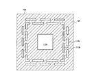
図6は、第3実施形態においてアライメントマークとして機能する第1開口部110の近傍を拡大した平面図である。本実施形態では、第1開口部110aの輪郭が矩形であり、第1開口部110の周囲に、各辺に沿って複数の第2開口部112b及び複数の第3開口部114bが配置されている。複数の第2開口部112bは、複数の棒状開口部を含む。本実施形態において、第2開口部112b及び第3開口部114bは、長方形もしくはL字形の例を示しているが、正方形であってもよい。
第3開口部114bは、隣接する第2開口部112bの間隙に対応する位置に配置されている。すなわち、第3開口部114bは、第1開口部110aから見て、隣接する第2開口部112bの間隙に重なる位置に配置されている。これにより、本実施形態の金属膜104は、第1開口部110aに向かう応力の伝達経路が第2開口部112b及び第3開口部114bによって塞がれた構成となっている。
以上の構成により、本実施形態では、フレーム102と金属膜104との境界から徐々に蓄積された応力が第2開口部112b及び第3開口部114bの配置された領域でリセットされ、第1開口部110aの縁まで伝達しない。したがって、第1開口部110aの縁が反ってしまうという問題が発生しないため、第1開口部110aをアライメントマークとして用いた正確な位置合わせが可能である。
本発明の実施形態として上述した各実施形態は、相互に矛盾しない限りにおいて、適宜組み合わせて実施することができる。また、各実施形態の蒸着マスクを基にして、当業者が適宜構成要素の追加、削除もしくは設計変更を行ったもの、又は、工程の追加、省略もしくは条件変更を行ったものも、本発明の要旨を備えている限り、本発明の範囲に含まれる。
また、上述した各実施形態の態様によりもたらされる作用効果とは異なる他の作用効果であっても、本明細書の記載から明らかなもの、又は、当業者において容易に予測し得るものについては、当然に本発明によりもたらされるものと解される。
100…蒸着マスク、102…フレーム、102a…開口部、104…金属膜、104a…マスク領域、107…画素用開口部、110、110a…第1開口部、112、112a、112b…第2開口部、114、114a、114b…第3開口部
Claims (10)
- フレームと、
前記フレームに保持された金属膜と、
を含み、
前記金属膜は、第1開口部と、前記第1開口部の周囲に配置された複数の第2開口部を有し、
前記第2開口部の最大幅は、前記第1開口部の最大幅よりも小さい、蒸着マスク。 - 前記複数の第2開口部は、前記第1開口部の輪郭に沿って配置される、請求項1に記載の蒸着マスク。
- 前記複数の第2開口部は、前記第1開口部の縁から、前記第1開口部の最大幅よりも大きい距離だけ離れた位置に配置される、請求項1に記載の蒸着マスク。
- 前記第1開口部の輪郭は、円形である、請求項1に記載の蒸着マスク。
- 前記金属膜の膜厚は、5~20μmである、請求項1に記載の蒸着マスク。
- 前記第1開口部の最大幅は0.5mm以上である、請求項1に記載の蒸着マスク。
- 前記第1開口部に対し前記複数の第2開口部より外側に配置された複数の第3開口部をさらに有する、請求項1に記載の蒸着マスク。
- 前記複数の第3開口部は、前記複数の第1開口部の輪郭に沿って配置される、請求項7に記載の蒸着マスク。
- 前記複数の第2開口部と前記複数の第3開口部は、前記第1開口部の輪郭に沿って環状に配置され、
隣接する2つの前記第2開口部の間のスペースに対向して、前記複数の第3開口部の1つが位置する、請求項7に記載の蒸着マスク。 - 前記第1開口部は、矩形であり、
前記複数の第2開口部は、互いに離間した複数の棒状開口部を含み、
隣接する2つの前記棒状開口部の間のスペースに対向して、前記複数の第3開口部の1つが位置する、請求項7に記載の蒸着マスク。
Priority Applications (2)
| Application Number | Priority Date | Filing Date | Title |
|---|---|---|---|
| CN201880039459.9A CN110741105A (zh) | 2017-06-28 | 2018-03-29 | 蒸镀掩模 |
| US16/693,454 US11111572B2 (en) | 2017-06-28 | 2019-11-25 | Vapor deposition mask |
Applications Claiming Priority (2)
| Application Number | Priority Date | Filing Date | Title |
|---|---|---|---|
| JP2017126165A JP6998139B2 (ja) | 2017-06-28 | 2017-06-28 | 蒸着マスク |
| JP2017-126165 | 2017-06-28 |
Related Child Applications (1)
| Application Number | Title | Priority Date | Filing Date |
|---|---|---|---|
| US16/693,454 Continuation US11111572B2 (en) | 2017-06-28 | 2019-11-25 | Vapor deposition mask |
Publications (1)
| Publication Number | Publication Date |
|---|---|
| WO2019003534A1 true WO2019003534A1 (ja) | 2019-01-03 |
Family
ID=64741357
Family Applications (1)
| Application Number | Title | Priority Date | Filing Date |
|---|---|---|---|
| PCT/JP2018/013198 Ceased WO2019003534A1 (ja) | 2017-06-28 | 2018-03-29 | 蒸着マスク |
Country Status (4)
| Country | Link |
|---|---|
| US (1) | US11111572B2 (ja) |
| JP (1) | JP6998139B2 (ja) |
| CN (1) | CN110741105A (ja) |
| WO (1) | WO2019003534A1 (ja) |
Families Citing this family (2)
| Publication number | Priority date | Publication date | Assignee | Title |
|---|---|---|---|---|
| US12037673B2 (en) * | 2018-09-27 | 2024-07-16 | Nippon Steel Chemical & Material Co., Ltd. | Metal mask material, method for manufacturing same, and metal mask |
| CN114446190B (zh) * | 2022-02-08 | 2023-07-25 | 武汉华星光电半导体显示技术有限公司 | 支撑板及显示装置 |
Citations (6)
| Publication number | Priority date | Publication date | Assignee | Title |
|---|---|---|---|---|
| JP2002060927A (ja) * | 2000-08-10 | 2002-02-28 | Toray Ind Inc | 薄膜パターン成膜用マスク |
| JP2009221535A (ja) * | 2008-03-17 | 2009-10-01 | Univ Of Tsukuba | 微細構造素子製造装置及び微細構造素子生産方法 |
| JP2012134043A (ja) * | 2010-12-22 | 2012-07-12 | Nitto Denko Corp | 有機el素子の製造方法及び製造装置 |
| JP2012522891A (ja) * | 2009-04-03 | 2012-09-27 | オスラム オプト セミコンダクターズ ゲゼルシャフト ミット ベシュレンクテル ハフツング | 材料堆積装置において基板を保持する装置 |
| JP2016009673A (ja) * | 2014-06-26 | 2016-01-18 | シャープ株式会社 | 有機エレクトロルミネッセンス素子製造用マスク、有機エレクトロルミネッセンス素子の製造装置、及び、有機エレクトロルミネッセンス素子の製造方法 |
| JP2017014582A (ja) * | 2015-07-02 | 2017-01-19 | 株式会社ブイ・テクノロジー | 成膜マスクの製造方法及びその製造装置 |
Family Cites Families (15)
| Publication number | Priority date | Publication date | Assignee | Title |
|---|---|---|---|---|
| JP2003017254A (ja) * | 2001-06-29 | 2003-01-17 | Sanyo Electric Co Ltd | エレクトロルミネッセンス表示装置の製造方法 |
| JP3596502B2 (ja) * | 2001-09-25 | 2004-12-02 | セイコーエプソン株式会社 | マスク及びその製造方法、エレクトロルミネッセンス装置及びその製造方法並びに電子機器 |
| JP2005042133A (ja) * | 2003-07-22 | 2005-02-17 | Seiko Epson Corp | 蒸着マスク及びその製造方法、表示装置及びその製造方法、表示装置を備えた電子機器 |
| JP4608874B2 (ja) * | 2003-12-02 | 2011-01-12 | ソニー株式会社 | 蒸着マスクおよびその製造方法 |
| JP2006152396A (ja) * | 2004-11-30 | 2006-06-15 | Sony Corp | メタルマスク、電鋳用マスク原版及びマスター原版の製造方法 |
| JP4624824B2 (ja) * | 2005-03-04 | 2011-02-02 | 京セラ株式会社 | メタルマスクの製造方法およびメタルマスク |
| JP2008293798A (ja) | 2007-05-24 | 2008-12-04 | Toyota Industries Corp | 有機el素子の製造方法 |
| JP5297046B2 (ja) * | 2008-01-16 | 2013-09-25 | キヤノントッキ株式会社 | 成膜装置 |
| JP2010106358A (ja) * | 2008-09-30 | 2010-05-13 | Canon Inc | 成膜用マスク及びそれを用いた成膜方法 |
| KR101135544B1 (ko) * | 2009-09-22 | 2012-04-17 | 삼성모바일디스플레이주식회사 | 마스크 조립체, 이의 제조 방법 및 이를 이용한 평판표시장치용 증착 장치 |
| US8786054B2 (en) * | 2009-11-16 | 2014-07-22 | Taiwan Semiconductor Manufacturing Company, Ltd. | Structure for integrated circuit alignment |
| KR101597887B1 (ko) * | 2010-12-20 | 2016-02-25 | 샤프 가부시키가이샤 | 증착 방법 및 증착 장치 |
| KR20160015214A (ko) * | 2013-04-22 | 2016-02-12 | 어플라이드 머티어리얼스, 인코포레이티드 | 능동적으로-정렬되는 미세 금속 마스크 |
| CN204125520U (zh) * | 2014-08-14 | 2015-01-28 | 昆山萬豐電子有限公司 | 一种用于磁控溅射工艺的立式掩膜夹具 |
| KR102509663B1 (ko) * | 2015-07-17 | 2023-03-14 | 도판 인사츠 가부시키가이샤 | 메탈 마스크용 기재의 제조 방법, 증착용 메탈 마스크의 제조 방법, 메탈 마스크용 기재, 및, 증착용 메탈 마스크 |
-
2017
- 2017-06-28 JP JP2017126165A patent/JP6998139B2/ja active Active
-
2018
- 2018-03-29 WO PCT/JP2018/013198 patent/WO2019003534A1/ja not_active Ceased
- 2018-03-29 CN CN201880039459.9A patent/CN110741105A/zh active Pending
-
2019
- 2019-11-25 US US16/693,454 patent/US11111572B2/en active Active
Patent Citations (6)
| Publication number | Priority date | Publication date | Assignee | Title |
|---|---|---|---|---|
| JP2002060927A (ja) * | 2000-08-10 | 2002-02-28 | Toray Ind Inc | 薄膜パターン成膜用マスク |
| JP2009221535A (ja) * | 2008-03-17 | 2009-10-01 | Univ Of Tsukuba | 微細構造素子製造装置及び微細構造素子生産方法 |
| JP2012522891A (ja) * | 2009-04-03 | 2012-09-27 | オスラム オプト セミコンダクターズ ゲゼルシャフト ミット ベシュレンクテル ハフツング | 材料堆積装置において基板を保持する装置 |
| JP2012134043A (ja) * | 2010-12-22 | 2012-07-12 | Nitto Denko Corp | 有機el素子の製造方法及び製造装置 |
| JP2016009673A (ja) * | 2014-06-26 | 2016-01-18 | シャープ株式会社 | 有機エレクトロルミネッセンス素子製造用マスク、有機エレクトロルミネッセンス素子の製造装置、及び、有機エレクトロルミネッセンス素子の製造方法 |
| JP2017014582A (ja) * | 2015-07-02 | 2017-01-19 | 株式会社ブイ・テクノロジー | 成膜マスクの製造方法及びその製造装置 |
Also Published As
| Publication number | Publication date |
|---|---|
| JP6998139B2 (ja) | 2022-01-18 |
| US11111572B2 (en) | 2021-09-07 |
| US20200095668A1 (en) | 2020-03-26 |
| CN110741105A (zh) | 2020-01-31 |
| JP2019007069A (ja) | 2019-01-17 |
Similar Documents
| Publication | Publication Date | Title |
|---|---|---|
| KR102776386B1 (ko) | 유기 발광 표시 장치의 픽셀 패터닝 및 픽셀 위치 검사 방법과 그 패터닝에 사용되는 마스크 | |
| JP7437159B2 (ja) | マスク、その製造方法、蒸着方法、及びディスプレイスクリーン | |
| CN112313801B (zh) | 阵列基板及其制作方法、显示装置 | |
| US7915073B2 (en) | Method of manufacturing the organic electroluminescent display and organic electroluminescent display manufactured by the method | |
| KR102616578B1 (ko) | 박막 증착용 마스크 어셈블리와, 이의 제조 방법 | |
| CN111051559B (zh) | 蒸镀掩模、显示面板的制造方法以及显示面板 | |
| WO2017215286A1 (zh) | 掩膜板以及掩膜板的组装方法 | |
| US20190203338A1 (en) | Vapor deposition mask, frame-equipped vapor deposition mask, method for producing organic semiconductor element, and method for producing organic el display | |
| US20160141498A1 (en) | High precision, high resolution collimating shadow mask and method for fabricating a micro-display | |
| US9780341B2 (en) | Shadow mask, method of manufacturing a shadow mask and method of manufacturing a display device using a shadow mask | |
| US20190386221A1 (en) | Mask assembly, deposition apparatus having the same, and method of fabricating display device using the same | |
| WO2016004698A1 (zh) | Oled显示器件及其制备方法、显示装置和蒸镀用掩模板 | |
| US20160289854A1 (en) | Manufacturing method of metal mask and mask for deposition using thereof | |
| WO2021046807A1 (zh) | 掩膜装置及其制造方法、蒸镀方法、显示装置 | |
| WO2019064420A1 (ja) | 蒸着マスク及び蒸着マスクの製造方法 | |
| KR101968066B1 (ko) | 증착용 메탈 마스크 | |
| KR20200092524A (ko) | 박막 증착용 마스크 프레임 어셈블리 | |
| JP2019526707A (ja) | メタルマスク、表示基板及びこれらの位置合わせ方法 | |
| US7387739B2 (en) | Mask and method of manufacturing the same, electroluminescent device and method of manufacturing the same, and electronic instrument | |
| WO2021226788A1 (zh) | 显示面板、掩模板、掩模板组件和制作掩模板组件的方法 | |
| CN111108229A (zh) | 蒸镀掩模以及蒸镀掩模的制造方法 | |
| US11111572B2 (en) | Vapor deposition mask | |
| US20060087226A1 (en) | Organic LED vapor deposition mask | |
| WO2017206792A1 (zh) | 用于oled面板的像素布图的掩膜结构、oled面板及其制作方法 | |
| CN111279012B (zh) | 蒸镀掩膜和显示装置的制造方法 |
Legal Events
| Date | Code | Title | Description |
|---|---|---|---|
| 121 | Ep: the epo has been informed by wipo that ep was designated in this application |
Ref document number: 18824770 Country of ref document: EP Kind code of ref document: A1 |
|
| NENP | Non-entry into the national phase |
Ref country code: DE |
|
| 122 | Ep: pct application non-entry in european phase |
Ref document number: 18824770 Country of ref document: EP Kind code of ref document: A1 |