WO2018230243A1 - ポジションセンサ - Google Patents
ポジションセンサ Download PDFInfo
- Publication number
- WO2018230243A1 WO2018230243A1 PCT/JP2018/019060 JP2018019060W WO2018230243A1 WO 2018230243 A1 WO2018230243 A1 WO 2018230243A1 JP 2018019060 W JP2018019060 W JP 2018019060W WO 2018230243 A1 WO2018230243 A1 WO 2018230243A1
- Authority
- WO
- WIPO (PCT)
- Prior art keywords
- detection
- bridge circuit
- center
- signal
- detection element
- Prior art date
- Legal status (The legal status is an assumption and is not a legal conclusion. Google has not performed a legal analysis and makes no representation as to the accuracy of the status listed.)
- Ceased
Links
Images


Classifications
-
- G—PHYSICS
- G01—MEASURING; TESTING
- G01D—MEASURING NOT SPECIALLY ADAPTED FOR A SPECIFIC VARIABLE; ARRANGEMENTS FOR MEASURING TWO OR MORE VARIABLES NOT COVERED IN A SINGLE OTHER SUBCLASS; TARIFF METERING APPARATUS; MEASURING OR TESTING NOT OTHERWISE PROVIDED FOR
- G01D5/00—Mechanical means for transferring the output of a sensing member; Means for converting the output of a sensing member to another variable where the form or nature of the sensing member does not constrain the means for converting; Transducers not specially adapted for a specific variable
- G01D5/12—Mechanical means for transferring the output of a sensing member; Means for converting the output of a sensing member to another variable where the form or nature of the sensing member does not constrain the means for converting; Transducers not specially adapted for a specific variable using electric or magnetic means
- G01D5/244—Mechanical means for transferring the output of a sensing member; Means for converting the output of a sensing member to another variable where the form or nature of the sensing member does not constrain the means for converting; Transducers not specially adapted for a specific variable using electric or magnetic means influencing characteristics of pulses or pulse trains; generating pulses or pulse trains
- G01D5/24428—Error prevention
- G01D5/24433—Error prevention by mechanical means
- G01D5/24438—Special design of the sensing element or scale
-
- G—PHYSICS
- G01—MEASURING; TESTING
- G01D—MEASURING NOT SPECIALLY ADAPTED FOR A SPECIFIC VARIABLE; ARRANGEMENTS FOR MEASURING TWO OR MORE VARIABLES NOT COVERED IN A SINGLE OTHER SUBCLASS; TARIFF METERING APPARATUS; MEASURING OR TESTING NOT OTHERWISE PROVIDED FOR
- G01D5/00—Mechanical means for transferring the output of a sensing member; Means for converting the output of a sensing member to another variable where the form or nature of the sensing member does not constrain the means for converting; Transducers not specially adapted for a specific variable
- G01D5/12—Mechanical means for transferring the output of a sensing member; Means for converting the output of a sensing member to another variable where the form or nature of the sensing member does not constrain the means for converting; Transducers not specially adapted for a specific variable using electric or magnetic means
- G01D5/14—Mechanical means for transferring the output of a sensing member; Means for converting the output of a sensing member to another variable where the form or nature of the sensing member does not constrain the means for converting; Transducers not specially adapted for a specific variable using electric or magnetic means influencing the magnitude of a current or voltage
- G01D5/142—Mechanical means for transferring the output of a sensing member; Means for converting the output of a sensing member to another variable where the form or nature of the sensing member does not constrain the means for converting; Transducers not specially adapted for a specific variable using electric or magnetic means influencing the magnitude of a current or voltage using Hall-effect devices
- G01D5/145—Mechanical means for transferring the output of a sensing member; Means for converting the output of a sensing member to another variable where the form or nature of the sensing member does not constrain the means for converting; Transducers not specially adapted for a specific variable using electric or magnetic means influencing the magnitude of a current or voltage using Hall-effect devices influenced by the relative movement between the Hall device and magnetic fields
-
- G—PHYSICS
- G01—MEASURING; TESTING
- G01B—MEASURING LENGTH, THICKNESS OR SIMILAR LINEAR DIMENSIONS; MEASURING ANGLES; MEASURING AREAS; MEASURING IRREGULARITIES OF SURFACES OR CONTOURS
- G01B7/00—Measuring arrangements characterised by the use of electric or magnetic techniques
-
- G—PHYSICS
- G01—MEASURING; TESTING
- G01D—MEASURING NOT SPECIALLY ADAPTED FOR A SPECIFIC VARIABLE; ARRANGEMENTS FOR MEASURING TWO OR MORE VARIABLES NOT COVERED IN A SINGLE OTHER SUBCLASS; TARIFF METERING APPARATUS; MEASURING OR TESTING NOT OTHERWISE PROVIDED FOR
- G01D11/00—Component parts of measuring arrangements not specially adapted for a specific variable
- G01D11/30—Supports specially adapted for an instrument; Supports specially adapted for a set of instruments
Definitions
- This disclosure relates to a position sensor that outputs a signal corresponding to a position to be detected.
- Patent Document 1 proposes a detection device configured to detect the movement of a detection target.
- a detection apparatus including a plurality of magnetoresistive elements and a processing circuit that processes the output of each magnetoresistive element has been proposed.
- Each magnetoresistive element constitutes a first magnetoresistive element pair and a second magnetoresistive element pair that are disposed at positions facing the detection target and electrically form a half-bridge circuit.
- the processing circuit outputs a binary signal obtained by binarizing the differential output by comparing the differential output of the midpoint potential of each magnetoresistive element pair with a threshold value.
- This disclosure is intended to provide a position sensor that can eliminate an inter-system error in a detection position even if the detection unit is configured in a double system.
- a position sensor includes a detection unit including a sensor chip having one surface, a first detection element provided in the sensor chip, and a second detection element provided in the sensor chip, and a detection unit And a signal processing unit for processing a signal input from.
- the first detection element outputs a first detection signal corresponding to the position of the detection target based on the change in the magnetic field received from the detection target, and the second detection element detects based on the change in the magnetic field received from the detection target.
- a second detection signal corresponding to the target position is output. Furthermore, the center of the balance of the first detection element in the surface of one surface coincides with the center of the balance of the second detection element in the surface of the one surface.
- each detection signal is a signal reflecting the average of the change in magnetic field at the center of balance of each detection element. Since the balance centers of the detection elements are coincident with each other, the averages of the changes in the magnetic field received by the detection elements from the detection object coincide. For this reason, each detection element can generate the same detection signal. Therefore, even if the detection unit is configured in a double system, it is possible to eliminate the intersystem error of the detection position.
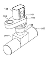
- FIG. 1 is an external view of a position sensor according to the first embodiment of the present disclosure.
- FIG. 2 is an exploded perspective view of components constituting a magnetic detection method using a magnetoresistive element
- FIG. 3 is a plan view of each component shown in FIG. 4 is a cross-sectional view taken along the line IV-IV in FIG.
- FIG. 5 is a diagram for explaining a detection signal by the magnetoresistive element
- FIG. 6 is a diagram showing a circuit configuration of the position sensor
- FIG. 7 is a diagram showing an equivalent circuit of the first magnetoresistive element pair
- FIG. 1 is an external view of a position sensor according to the first embodiment of the present disclosure.
- FIG. 2 is an exploded perspective view of components constituting a magnetic detection method using a magnetoresistive element
- FIG. 5 is a diagram for explaining a detection signal by the
- FIG. 8 is a plan view showing a layout of each resistance portion of each half-bridge circuit
- FIG. 9 is a diagram showing output voltages G1 and G2 of each half bridge circuit.
- FIG. 10 is a diagram showing detection signals and state determinations when detecting three states.
- FIG. 11 is a diagram showing a configuration in which each system is provided in a separate sensor chip as a comparative example
- FIG. 12 is a diagram showing output voltages G1 and G2 of each half bridge circuit in the configuration shown in FIG.
- FIG. 13 is a diagram showing a configuration in which each system is provided in one sensor chip as a comparative example.
- FIG. 14 is a diagram showing output voltages G1 and G2 of each half-bridge circuit in the configuration shown in FIG. FIG.
- FIG. 15 is a diagram showing a case where the wiring patterns of all the resistance portions are formed to be the same as a modified example
- FIG. 16 is a diagram showing a case where each half-bridge circuit is driven by a current source as a modification
- FIG. 17 is a diagram showing a configuration in which each half-bridge circuit has four resistance units as a modification
- FIG. 18 is a diagram showing a layout of each resistance unit shown in FIG.
- FIG. 19 is a diagram showing a case where the wiring pattern of each resistance portion is formed unevenly as a modified example.
- FIG. 20 is a diagram showing a case where the wiring pattern of each resistance portion is formed unevenly as a modification.
- FIG. 20 is a diagram showing a case where the wiring pattern of each resistance portion is formed unevenly as a modification.
- FIG. 21 is a diagram showing a case where the wiring patterns of the respective resistance portions are formed symmetrically as a modification example.
- FIG. 22 is a diagram showing a case in which the wiring patterns of the respective resistance portions are formed so as to coexist as a modification example.
- FIG. 23 is a plan view of a sensor chip according to the second embodiment, 24 is a sectional view taken along line XXIV-XXIV in FIG.
- FIG. 25 is a plan view showing components constituting a magnetic detection method using a Hall element in the third embodiment.
- 26 is a cross-sectional view taken along the line XXVI-XXVI of FIG.
- FIG. 27 is a diagram for explaining a detection signal by the Hall element.
- FIG. 28 is a plan view showing the layout of three Hall elements
- FIG. 29 is a diagram showing signals G3 and G4 of each system
- FIG. 30 is a diagram showing detection signals and state determinations when three states are detected by the Hall element
- FIG. 31 is a plan
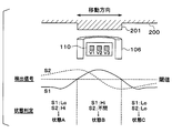
- the position sensor according to the present embodiment is a sensor that detects which range (state) the position of the detection target is in and outputs a signal corresponding to the range.
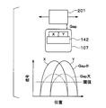
- the position sensor 100 detects the position of the shaft 200 interlocked with the operation of the shift position of the vehicle as a detection target. Specifically, the position sensor 100 acquires the state of the shaft 200 by detecting a signal corresponding to the position of the protrusion 201 provided on the shaft 200.
- the state of the shaft 200 means the position of the shaft 200 when the shift position is operated by the user.
- the shaft 200 moves in conjunction with parking at the shift position.
- the shaft 200 moves in the axial direction.
- the shaft 200 reflects the state of parking.
- the position sensor 100 detects the position of the shaft 200 in front of the protrusion 201.
- the shaft 200 reflects a state other than parking.
- the position sensor 100 detects the protrusion 201 and the position behind the protrusion 201 in the shaft 200.
- the shaft 200 may be moved in conjunction with a position other than parking.
- the shaft 200 is entirely made of a magnetic material, for example.
- the shaft 200 may have a surface facing the position sensor 100 of the protruding portion 201 formed of a magnetic material, and the other portion formed of another metal material.
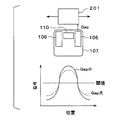
- the position sensor 100 includes a case 101 formed by resin molding of a resin material such as PPS.
- the case 101 has a tip portion 102 on the shaft 200 side, a flange portion 103 fixed to the peripheral mechanism, and a connector portion 104 to which a harness is connected.
- a sensing portion is provided inside the tip portion 102.
- the position sensor 100 is fixed to the peripheral mechanism via the flange portion 103 so that the tip portion 102 has a predetermined gap with respect to the protruding portion 201 of the shaft 200. Accordingly, the shaft 200 moves with respect to the position sensor 100.
- the position sensor 100 may be fixed to a peripheral mechanism so as to detect the position of a valve that operates in conjunction with the shaft 200.
- the moving direction of the shaft 200 is not limited to linear movement or reciprocation, but may be rotation, reciprocation within a specific angle, or the like.
- the position sensor 100 can be applied to state detection such as the position, movement, and rotation of the movable part that moves in conjunction with the operation of the shift position of the vehicle.
- the position sensor 100 employs a magnetic detection method using a magnetoresistive element.
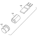
- the position sensor 100 includes a mold IC unit 105, a magnet 106, and a holding unit 107. These are housed in the tip portion 102 of the case 101.
- the mold IC part 105 is inserted into the hollow cylindrical magnet 106.
- the magnet 106 is inserted into the bottomed cylindrical holding portion 107.
- the mold IC part 105, the magnet 106, and the holding part 107 are integrated.
- the main part of the mold IC part 105 is located in the hollow part of the magnet 106.
- the holding unit 107 fixes the positions of the mold IC unit 105 and the magnet 106.
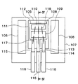
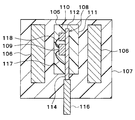
- the mold IC part 105 includes a lead frame 108, a processing circuit chip 109, a sensor chip 110, and a mold resin part 111.
- the lead frame 108 has a plate-like island portion 112 and a plurality of leads 113 to 115.
- the island part 112 is arranged so that the plane part is perpendicular to the moving direction of the detection target.
- the plurality of leads 113 to 115 correspond to a power supply terminal 113 to which a power supply voltage is applied, a ground terminal 114 to which a ground voltage is applied, and an output terminal 115 for outputting a signal. That is, each of the leads 113 to 115 has three wires for power supply, ground, and signal. Terminals 116 are connected to the tips of the leads 113 to 115, respectively. The terminal 116 is located in the connector part 104 of the case 101. A terminal 116 is connected to the harness.
- the ground lead 114 among the plurality of leads 113 to 115 is integrated with the island portion 112.
- the island portion 112 and all the leads 113 to 115 may be completely separated.
- the processing circuit chip 109 and the sensor chip 110 are mounted on the island portion 112 with an adhesive or the like.
- the processing circuit chip 109 constitutes a circuit unit that processes signals from the sensor chip 110.
- the sensor chip 110 includes a magnetoresistive element whose resistance value changes when affected by a magnetic field from the outside.
- the magnetoresistive element is, for example, AMR, GMR, or TMR.
- Each lead 113 to 115 and the processing circuit chip 109 are electrically connected via a wire 117.
- the processing circuit chip 109 and the sensor chip 110 are electrically connected via a wire 118.
- the mold resin part 111 seals the island part 112, a part of each of the leads 113 to 115, the processing circuit chip 109, and the sensor chip 110.
- the mold resin portion 111 is molded into a shape that is fixed to the hollow portion of the magnet 106.
- the holding unit 107 is arranged with a predetermined gap with respect to the protrusion 201 that is a detection target.
- the detection signal becomes maximum at the center of the movement direction of the protrusion 201.
- the gap increases, the amplitude of the detection signal decreases, and when the gap decreases, the amplitude of the detection signal increases.
- the detection signal is generated by outputs of a plurality of magnetoresistive elements.
- the magnetoresistive element that detects a magnetic vector has an advantage that an accuracy error due to a gap shift can be canceled. Further, there is a merit that the influence of the stress generated in the sensor chip 110 can be reduced or canceled. Therefore, highly accurate detection is possible.
- the circuit configuration configured in the sensor chip 110 and the processing circuit chip 109 will be described.
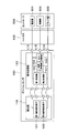
- the position sensor 100 and the controller 300 are electrically connected via a harness 400.
- the harness 400 is constituted by three wires.
- the controller 300 is, for example, a transmission controller (TCU).
- the controller 300 includes a power supply unit 301, a control unit 302, and a ground unit 303.
- the power supply unit 301 is a circuit unit that supplies a power supply voltage to the position sensor 100.
- the control unit 302 is a circuit unit that performs predetermined control according to an output signal input from the position sensor 100.
- the ground unit 303 is a circuit unit that sets the ground voltage of the position sensor 100.
- the controller 300 may be configured as an electronic control unit (ECU).
- the position sensor 100 includes a detection unit 119 and a signal processing unit 120.
- the detection unit 119 is provided on the sensor chip 110.
- the signal processing unit 120 is provided in the processing circuit chip 109.
- the detection unit 119 and the signal processing unit 120 operate based on the power supply voltage and the ground voltage supplied from the controller 300.
- the detection unit 119 includes a first magnetoresistive element 121 and a second magnetoresistive element 122.
- the first magnetoresistive element 121 is configured to output a first detection signal corresponding to the position of the protrusion 201.
- the second magnetoresistive element 122 is configured to output a second detection signal corresponding to the position of the protrusion 201.
- Each of the magnetoresistive elements 121 and 122 has three element pairs of a first magnetoresistive element pair, a second magnetoresistive element pair, and a third magnetoresistive element pair whose resistance value changes as the protrusion 201 moves. is doing.
- Each is arranged so that the second magnetoresistive element pair is located between the first magnetoresistive element pair and the third magnetoresistive element pair in the moving direction of the protrusion 201. That is, the second magnetoresistive element pair is disposed so as to be sandwiched between the first magnetoresistive element pair and the third magnetoresistive element pair.
- a bias magnetic field along the central axis of the magnet 106 is applied to the second magnetoresistive element pair.
- a bias magnetic field for winding the end of the magnet 106 is applied to the first magnetoresistive element pair and the third magnetoresistive element pair.
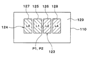
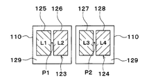
- Each magnetoresistive element pair is configured as a half bridge circuit in which two resistance units are connected in series between a power source and a ground.
- the first magnetoresistive element pair includes a first half bridge circuit 123 constituting a part of the first magnetoresistive element 121 and a part of the second magnetoresistive element 122.
- a second half-bridge circuit 124 that constitutes
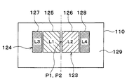
- the first half-bridge circuit 123 is configured by connecting two resistance units 125 and 126 (L1, L2) in series.
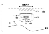
- the resistance values of the resistance portions 125 and 126 change when the two resistance portions 125 and 126 are affected by the magnetic field as the protrusion 201 moves. Therefore, the first half bridge circuit 123 outputs the voltage G1 at the midpoint between the two resistance units 125 and 126 as a waveform signal based on the change in the resistance value.
- This voltage G1 is one of the signals of the first system of the double system.
- the second half bridge circuit 124 In the second half bridge circuit 124, two resistance units 127 and 128 (L3 and L4) are connected in series. Similarly to the above, the second half bridge circuit 124 outputs the voltage G2 at the midpoint between the two resistance units 127 and 128 as a waveform signal based on the change in the resistance value of each of the resistance units 127 and 128. This voltage G2 is one of the signals of the second system of the double system.
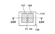
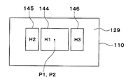
- the half-bridge circuits 123 and 124 are arranged on the one surface 129 of the sensor chip 110 so that the balance centers of the wiring patterns coincide.
- the case where the sensor chip 110 is disposed on the one surface 129 is not only the case where the sensor chip 110 is disposed directly on the one surface 129 but also the case where the sensor chip 110 is disposed on a protective film or the like formed on the one surface 129. Is also included.
- the wiring pattern of the second half bridge circuit 124 is a layout in which the wiring pattern of the first half bridge circuit 123 is sandwiched on one surface 129 of the sensor chip 110. Specifically, the first half-bridge circuit 123 is laid out so that the resistor portions 125 and 126 are adjacent to each other. In addition, the wiring patterns of the resistance portions 125 and 126 are formed, for example, in a rectangular region, and the linear portions of the wiring are formed in line symmetry so as to follow the oblique lines in FIG. Accordingly, the center of the balance of the wiring pattern of the first half bridge circuit 123 is P1 in FIG.
- the resistance parts 127 and 128 of the second half bridge circuit 124 are laid out so as to be separated from each other.
- the resistor units 125 and 126 of the first half bridge circuit 123 are sandwiched between the resistor unit 127 and the resistor unit 128.
- the wiring patterns of the resistance portions 127 and 128 are formed in a rectangular area, and the straight line portions of the wiring are formed in line symmetry so as to follow the oblique lines in FIG. Accordingly, the center of the balance of the wiring pattern of the second half bridge circuit 124 is P2 in FIG.
- the center of the balance of the wiring pattern of the first half-bridge circuit 123 in the plane of the one surface 129 of the sensor chip 110 is the center of the balance of the wiring pattern of the second half-bridge circuit 124 in the plane of the one surface 129 of the sensor chip 110.
- the center of balance is a position where the balance of the resistance portions 125 and 126 and the resistance portions 127 and 128 is balanced, such as the center of layout, the center of gravity of the area, or the center of gravity of the wiring pattern. Therefore, as in the second half-bridge circuit 124, even if the resistor units 127 and 128 are separated from each other, the position of the resistor units 127 and 128 and the center position of the balance are not related.
- the average of the magnetic field direction changes received by the resistance portions 125 and 126 of the first half bridge circuit 123 is the change in the voltage G1.
- the change in the voltage G1 is a signal reflecting the change in the magnetic field direction at the center of the balance of the wiring pattern of the first half bridge circuit 123.
- the average of the magnetic field direction changes received by the respective resistance units 127 and 128 of the second half bridge circuit 124 is the change in the voltage G2.
- the change in the voltage G2 is a signal reflecting the change in the magnetic field direction at the center of the balance of the wiring pattern of the second half bridge circuit 124.
- the first magnetoresistive element pair detects a change in the resistance value of each of the resistance units 125 and 126 and each of the resistance units 127 and 128 when affected by the magnetic field as the projection 201 moves.
- the first magnetoresistive element pair outputs the voltages G1 and G2 at the midpoints of the half-bridge circuits 123 and 124 as waveform signals based on the change in the resistance value.
- the signal G1 output from the first half bridge circuit 123 and the signal G2 output from the second half bridge circuit 124 are exactly the same waveform signals. That is, there is no deviation between the signals G1 and G2 between the first system and the second system of the double system.
- the second magnetoresistive element pair and the third magnetoresistive element pair are also composed of two half-bridge circuits 123 and 124 in the same manner as described above. That is, the second magnetoresistive element pair is also configured by the first half bridge circuit 123 and the second half bridge circuit 124. The same applies to the third magnetoresistive element pair. That is, the first magnetoresistive element 121 has three element pairs, and has three first half bridge circuits 123 constituting each element pair. Similarly, the second magnetoresistive element 122 has three element pairs and three second half-bridge circuits 124 constituting each element pair. In FIG. 9, only the first magnetoresistive element pair is shown in the sensor chip 110, but actually three element pairs are provided in the sensor chip 110.
- the magnetoresistive elements 121 and 122 include first to fourth operational amplifiers. Each operational amplifier is provided for each of the magnetoresistive elements 121 and 122.
- the midpoint potential of the first half-bridge circuit 123 of the first magnetoresistive element pair is V1
- the midpoint potential of the first half-bridge circuit 123 of the second magnetoresistive element pair is V2
- the third The midpoint potential of the first half bridge circuit 123 of the magnetoresistive element pair is defined as V3.
- the first operational amplifier is a differential amplifier configured to calculate V1-V2 and output the result as R1.
- the second operational amplifier is a differential amplifier configured to calculate V2-V3 and output the result as R2.
- the third operational amplifier is a differential amplifier configured to calculate V1-V3 and output the result as S1.
- the signal S ⁇ b> 1 is a signal having a waveform in which the amplitude is maximum at the center of the movement direction of the protrusion 201 of the shaft 200 and is minimum at a position away from the protrusion 201.
- the signal of S2 is a waveform signal corresponding to the concavo-convex structure of the protrusion 201 of the shaft 200.
- the signal S2 is a signal having a waveform in which the amplitude is maximum at one edge portion where the protrusion 201 of the shaft 200 is switched from the concave to the convex and the amplitude is minimum at the other edge portion where the convex is switched to the concave.
- This signal S2 is a waveform signal having a phase difference with respect to the signal S1.
- the first magnetoresistive element 121 outputs the signal S1 and the signal S2 to the signal processing unit 120 as the first detection signal.
- the second magnetoresistive element 122 outputs the signal S1 and the signal S2 to the signal processing unit 120 as the second detection signal.
- Each operational amplifier may be provided in the signal processing unit 120. That is, each detection signal may be configured to be acquired by the signal processing unit 120.
- the signal processing unit 120 in FIG. 6 is a circuit unit that processes a signal input from the detection unit 119.
- the signal processing unit 120 includes a first processing unit 130, a second processing unit 131, a failure determination unit 132, and an output circuit unit 133.
- the first processing unit 130 receives the first detection signal from the first magnetoresistive element 121, and specifies the position of the protrusion 201 based on the first detection signal.
- the second processing unit 131 receives the second detection signal from the second magnetoresistive element 122 and specifies the position of the protrusion 201 based on the second detection signal. Therefore, each of the processing units 130 and 131 has a threshold for the detection signal.
- each of the processing units 130 and 131 compares the signals S1 and S2, which are detection signals, with a threshold value. Each of the processing units 130 and 131 determines Hi when the signals S1 and S2 are larger than the threshold, and determines Lo when the signals S1 and S2 are smaller than the threshold. Further, the processing units 130 and 131 determine which range of the shaft 200 is detected by the magnetoresistive elements 121 and 122 from the Hi / Lo combinations of the signals S1 and S2.
- each of the magnetoresistive elements 121 and 122 has detected a range on the left side of the drawing from the protrusion 201 of the shaft 200. become. That is, each processing unit 130, 131 has specified the position of the shaft 200.
- the state of the shaft 200 when the position of the range is specified is referred to as “state A”.
- each of the magnetoresistive elements 121 and 122 has detected the range on the right side of the drawing from the protrusion 201 of the shaft 200.
- the state of the shaft 200 when the position of the range is specified is referred to as “state C”.
- each of the processing units 130 and 131 specifies the position of the shaft 200 as a position in any one of a plurality of ranges along the moving direction of the shaft 200.
- first magnetoresistive element 121 and the first processing unit 130 constitute a first system.
- second magnetoresistive element 122 and the second processing unit 131 constitute a second system.
- each of the processing units 130 and 131 may output, to the failure determination unit 132, a signal having a value corresponding to a specified position range among discrete values set in a plurality of ranges.
- the discrete value signal is, for example, a voltage signal having a different voltage value or a pulse signal having a different pulse width.
- the failure determination unit 132 is a circuit unit that determines whether the position specified by the first processing unit 130 matches the position specified by the second processing unit 131.
- the positions specified by the processing units 130 and 131 are the types of the states A to C described above. Therefore, the failure determination unit 132 determines whether or not the states specified by the processing units 130 and 131 match.
- the failure determination unit 132 outputs the result of the failure determination to the output circuit unit 133.
- the output circuit unit 133 is a circuit unit that controls a signal output to the controller 300 based on the determination result of the failure determination unit 132. When the determination by the failure determination unit 132 matches, the output circuit unit 133 outputs a position signal corresponding to the matching position to the output terminal 115. On the other hand, the output circuit unit 133 outputs a failure signal corresponding to the failure to the output terminal 115 when the determination by the failure determination unit 132 does not match.
- the above is the configuration of the position sensor 100 according to the present embodiment.
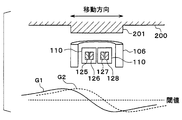
- each system is provided in a separate sensor chip 110 as shown in FIG.
- the first half bridge circuit 123 of the first system is provided in one sensor chip 110.
- the center of the balance of the wiring pattern of the first half bridge circuit 123 is P1 in FIG.
- the second sensor chip 110 is provided with a second half bridge circuit 124 of the second system.
- the center of the balance of the wiring pattern of the second half bridge circuit 124 is P2 in FIG.
- the equivalent circuit is the same as in FIG.
- the half bridge circuits 123 and 124 may be provided in one sensor chip 110. However, since the resistance parts 125 and 126 of the first half bridge circuit 123 are laid out next to each other and the resistance parts 127 and 128 of the second half bridge circuit 124 are laid out next to each other, the half bridge circuits 123 are arranged. , 124 does not match the balance center of the wiring pattern. Therefore, also in this case, as shown in FIG. 14, a phase difference occurs between the voltages G1 and G2 of the half-bridge circuits 123 and 124.
- the balance centers of the wiring patterns of the half-bridge circuits 123 and 124 coincide with each other, so that the magnetoresistive elements 121 and 122 change in the magnetic field received from the shaft 200.
- the averages match.
- the same detection signal can be generated in each system. Therefore, even if the detection unit 119 is configured in a double system, it is possible to eliminate the intersystem error of the detection position. In this way, no inter-system error in the detection signal occurs, and no position detection error occurs between the systems, so that the same position can be detected in each of the dual systems.
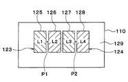
- each of the resistance portions 125 and 126 of the first half bridge circuit 123 may be formed in the same direction so that the straight line portion of the wiring follows the oblique line in FIG. 15. The same applies to the resistance units 127 and 128 of the second half bridge circuit 124.
- the first half bridge circuit 123 may be configured to operate by a current source 134 as shown in FIG. In this case, the voltage G1 across the first half bridge circuit 123 is output. The same applies to the second half bridge circuit 124.
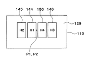
- the first half-bridge circuit 123 is configured as a series connection of four resistance units 125, 126, 135, and 136 (L 1 to L 4), and the second half-bridge circuit 124 includes 4 Two resistor parts 127, 128, 137, and 138 (L5 to L8) may be connected in series.
- the first half-bridge circuit 123 outputs the voltage G1 at the connection part between the resistance part 126 and the resistance part 135.
- the second half bridge circuit 124 outputs a voltage G2 at a connection portion between the resistance unit 128 and the resistance unit 137.
- the resistance portions 125, 126, 135, and 136 of the first half bridge circuit 123 are arranged in a cross shape.
- the resistor 126 (L2) is disposed at a diagonal position of the resistor 125 (L1).
- the resistor 136 (L4) is disposed at a diagonal position of the resistor 135 (L3).
- the resistance parts 135 and 136 are located next to the resistance parts 125 and 126.
- the direction of the wiring pattern is also a cross shape.
- the center of the balance of the wiring patterns of the four resistance portions 125, 126, 135, and 136 is P1 in FIG.
- the resistance units 127, 128, 137, and 138 of the second half-bridge circuit 124 are arranged in a cross shape as described above, but the resistance unit 127, the resistance unit 138, the resistance unit 137, and the resistance unit 128 are arranged. It is laid out to be located apart.
- the center of the balance of the wiring patterns of the four resistance portions 127, 128, 137, and 138 is P2 in FIG. 18 and coincides with the center of the balance of the wiring pattern of the first half bridge circuit 123.
- P2 in FIG. 18 coincides with the center of the balance of the wiring pattern of the first half bridge circuit 123.
- the wiring patterns of the half-bridge circuits 123 and 124 may be formed unevenly. Even in such a case, the balance centers of the wiring patterns of the half-bridge circuits 123 and 124 coincide with each other. If the wiring pattern is non-uniform, it may be designed so that the area centroids of the wiring pattern coincide. In addition, as shown in FIG. 20, by designing the wiring pattern so that a certain region is provided, it becomes possible to arrange elements such as transistors in the wiring pattern.
- the wiring patterns of the half-bridge circuits 123 and 124 may be formed symmetrically.
- the resistance portions 125 and 126 of the first half bridge circuit 123 are formed in a wide region
- the resistance portions 127 and 128 of the second half bridge circuit 124 are formed in a narrow region.
- the wiring pattern of the first half bridge circuit 123 and the wiring pattern of the second half bridge circuit 124 are mixedly formed on one surface 129 of the sensor chip 110. Also good. Even in such a case, the balance centers of the wiring patterns of the half-bridge circuits 123 and 124 can be matched.
- the shaft 200 corresponds to “detection target”.
- the magnetoresistive elements 121 and 122 correspond to “detection elements”.
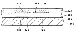
- the first half-bridge circuit 123 and the second half-bridge circuit 124 are arranged in a layered manner on the one surface 129 of the sensor chip 110.
- the wiring patterns of the half bridge circuits 123 and 124 are provided in layers so that the wiring pattern of the first half bridge circuit 123 is positioned on the one surface 129 side of the sensor chip 110.
- the resistance portions 125 and 126 of the first half bridge circuit 123 are formed on one surface 129 of the sensor chip 110.
- An interlayer insulating film 139 is formed on one surface 129 of the sensor chip 110 so as to cover the resistance portions 125 and 126.
- the resistance portions 127 and 128 of the second half bridge circuit 124 are formed on the interlayer insulating film 139.
- a protective film 140 is formed on the interlayer insulating film 139 so as to cover the resistance portions 127 and 128.
- the resistor 127 is positioned on the resistor 125, and the resistor 128 is positioned on the resistor 126.
- the center of the balance of the wiring patterns of the half-bridge circuits 123 and 124 is within the surface 129 of the sensor chip 110. Match. Therefore, the same effect as the first embodiment can be obtained.
- the wiring pattern may be provided in layers so that the wiring pattern of the second half bridge circuit 124 is positioned on the one surface 129 side of the sensor chip 110.
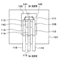
- the mold IC part 105 is inserted into the holding part 107 and fixed as shown in the schematic plan view of FIG. 25 and the schematic sectional view of FIG.
- the mold IC part 105 includes a lead frame 108, an IC chip 141, a magnet 142, and a mold resin part 111.
- the island part 112 of the lead frame 108 is arranged so that the plane part is parallel to the moving direction of the detection target.
- the leads 113 to 115 are arranged so as to be perpendicular to the moving direction of the detection target.
- a ground lead 114 is integrated with the island portion 112 at a right angle. Terminals 116 are connected to the tips of the leads 113 to 115, respectively.
- the IC chip 141 is formed with a plurality of Hall elements and a signal processing circuit unit. That is, the magnetic detection system using the Hall element has a one-chip configuration.
- the magnet 142 is fixed to the surface of the island part 112 opposite to the IC chip 141.
- Each of the leads 113 to 115 and the IC chip 141 are electrically connected via a wire 143.
- the mold resin part 111 is molded into a shape that is fixed to the hollow part of the holding part 107.
- a detection signal by a magnetic detection method using a Hall element will be described. As shown in FIG. 27, for example, when two Hall elements (X, Y) are arranged above the magnet 142, when the protrusion 201 moves with respect to the holding part 107, each Hall element (X, Y) is moved. ), Each detection signal becomes maximum. The relationship between the gap and the amplitude of the detection signal is the same as in the magnetic detection method using the magnetoresistive element. By setting a threshold value for each detection signal, the position of the protrusion 201 can be detected.
- a double system can be constituted by three Hall elements 144 to 146 (H1 to H3).
- the Hall element 144 outputs a first system signal.
- the hall element 144 is formed in, for example, a rectangular area.
- the center of balance of the Hall element 144 is P1 in FIG.
- the output h1 of the hall element 144 is defined as a first system signal G3.
- the Hall elements 145 and 146 output signals of the second system.
- the hall elements 145 and 146 are laid out so as to be located apart from each other.
- the Hall element 144 of the first system is sandwiched between the Hall elements 145 and 146.
- Each Hall element 145, 146 is formed in a rectangular region.
- the center of balance of each Hall element 145, 146 is P2 in FIG.
- the sum (h2 + h3) of the output h2 of the Hall element 145 and the output h3 of the Hall element 146 is defined as a second system signal G4.
- the first system signal G3 and the second system signal G4 have the same waveform signal. As described above, even when the Hall elements 144 to 146 are used, there is no deviation between the signals G3 and G4 between the first system and the second system of the double system.
- the three detection elements 147 to 149 each constitute a double system.
- the detection unit 119 outputs the first system signals S3 and S4 to the signal processing unit 120 as the first detection signals and the second system signals S3 and S4 as the second detection signals.
- FIG. 30 shows one system. And state determination is performed similarly to the case of FIG. 10 of 1st Embodiment.
- a double system may be configured by four Hall elements 144 to 146, 150 (H1 to H4).
- the arrangement of the Hall elements 144 to 146, 150 in this case is the same as that in FIG.
- the Hall elements 144 and 150 constituting the first system correspond to the “first detection element”, and the Hall elements 145 and 146 constituting the second system correspond to the “second detection element”.
- the configuration of the position sensor 100 shown in each of the above embodiments is an example, and is not limited to the configuration shown above, and other configurations that can realize the present disclosure can be used.
- the use of the position sensor 100 is not limited to a vehicle, and can be widely used for industrial robots, manufacturing facilities, and the like as detecting the position of a movable part.
Landscapes
- Physics & Mathematics (AREA)
- General Physics & Mathematics (AREA)
- Transmission And Conversion Of Sensor Element Output (AREA)
- Measurement Of Length, Angles, Or The Like Using Electric Or Magnetic Means (AREA)
Priority Applications (3)
| Application Number | Priority Date | Filing Date | Title |
|---|---|---|---|
| DE112018003054.7T DE112018003054T5 (de) | 2017-06-16 | 2018-05-17 | Positionssensor |
| CN201880039451.2A CN110741230B (zh) | 2017-06-16 | 2018-05-17 | 位置传感器 |
| US16/697,902 US11733063B2 (en) | 2017-06-16 | 2019-11-27 | Position sensor |
Applications Claiming Priority (2)
| Application Number | Priority Date | Filing Date | Title |
|---|---|---|---|
| JP2017-118778 | 2017-06-16 | ||
| JP2017118778A JP6743770B2 (ja) | 2017-06-16 | 2017-06-16 | ポジションセンサ |
Related Child Applications (1)
| Application Number | Title | Priority Date | Filing Date |
|---|---|---|---|
| US16/697,902 Continuation US11733063B2 (en) | 2017-06-16 | 2019-11-27 | Position sensor |
Publications (1)
| Publication Number | Publication Date |
|---|---|
| WO2018230243A1 true WO2018230243A1 (ja) | 2018-12-20 |
Family
ID=64660839
Family Applications (1)
| Application Number | Title | Priority Date | Filing Date |
|---|---|---|---|
| PCT/JP2018/019060 Ceased WO2018230243A1 (ja) | 2017-06-16 | 2018-05-17 | ポジションセンサ |
Country Status (5)
| Country | Link |
|---|---|
| US (1) | US11733063B2 (enExample) |
| JP (1) | JP6743770B2 (enExample) |
| CN (1) | CN110741230B (enExample) |
| DE (1) | DE112018003054T5 (enExample) |
| WO (1) | WO2018230243A1 (enExample) |
Cited By (2)
| Publication number | Priority date | Publication date | Assignee | Title |
|---|---|---|---|---|
| US11099034B2 (en) | 2017-06-16 | 2021-08-24 | Denso Corporation | Position sensor |
| US11493528B2 (en) | 2017-06-14 | 2022-11-08 | Denso Corporation | Position sensor |
Families Citing this family (3)
| Publication number | Priority date | Publication date | Assignee | Title |
|---|---|---|---|---|
| JP7422051B2 (ja) * | 2020-11-02 | 2024-01-25 | 株式会社デンソー | ポジションセンサ |
| JP7332738B2 (ja) | 2021-07-08 | 2023-08-23 | Tdk株式会社 | 磁気センサ装置および磁気センサシステム |
| CN113418440A (zh) * | 2021-08-05 | 2021-09-21 | 重庆编福科技有限公司 | 一种非接触式位置检测方法 |
Citations (3)
| Publication number | Priority date | Publication date | Assignee | Title |
|---|---|---|---|---|
| JP2009139252A (ja) * | 2007-12-07 | 2009-06-25 | Tokai Rika Co Ltd | ポジションセンサ |
| US20130300409A1 (en) * | 2011-01-17 | 2013-11-14 | Jiangsu Multidimensional Technology Co., Ltd | Single-Package Bridge-Type Magnetic Field Sensor |
| WO2015008439A1 (ja) * | 2013-07-17 | 2015-01-22 | 株式会社デンソー | 回転センサ |
Family Cites Families (15)
| Publication number | Priority date | Publication date | Assignee | Title |
|---|---|---|---|---|
| US6452381B1 (en) * | 1997-11-28 | 2002-09-17 | Denso Corporation | Magnetoresistive type position detecting device |
| JP4293037B2 (ja) * | 2004-04-13 | 2009-07-08 | 株式会社デンソー | 回転検出装置 |
| JP4466355B2 (ja) | 2004-06-23 | 2010-05-26 | 株式会社デンソー | 回転検出装置 |
| JP2006300779A (ja) | 2005-04-21 | 2006-11-02 | Denso Corp | 回転検出装置 |
| JP2009014454A (ja) * | 2007-07-03 | 2009-01-22 | Tokai Rika Co Ltd | 位置検出装置 |
| EP2446287B1 (en) * | 2009-07-22 | 2013-10-02 | Allegro Microsystems, LLC | Circuits and methods for generating a diagnostic mode of operation in a magnetic field sensor |
| JP5249156B2 (ja) | 2009-08-21 | 2013-07-31 | 株式会社東海理化電機製作所 | 多重系磁気センサのセンサパターン配置構造及びその製造方法 |
| JP2015108527A (ja) | 2013-12-03 | 2015-06-11 | 株式会社東海理化電機製作所 | 磁気センサ |
| JP2015129700A (ja) * | 2014-01-08 | 2015-07-16 | アルプス電気株式会社 | 磁界回転検知センサ及び磁気エンコーダ |
| US9719806B2 (en) | 2014-10-31 | 2017-08-01 | Allegro Microsystems, Llc | Magnetic field sensor for sensing a movement of a ferromagnetic target object |
| CN105890507B (zh) * | 2015-01-08 | 2019-04-16 | 中国人民解放军军械工程学院 | 一种巨磁阻抗传感器对平面内磁性目标的定位方法 |
| US10012518B2 (en) * | 2016-06-08 | 2018-07-03 | Allegro Microsystems, Llc | Magnetic field sensor for sensing a proximity of an object |
| JP2019002469A (ja) | 2017-06-14 | 2019-01-10 | 株式会社デンソー | ポジションセンサ |
| JP6787260B2 (ja) | 2017-06-14 | 2020-11-18 | 株式会社デンソー | ポジションセンサ |
| JP6791033B2 (ja) | 2017-06-16 | 2020-11-25 | 株式会社デンソー | ポジションセンサ |
-
2017
- 2017-06-16 JP JP2017118778A patent/JP6743770B2/ja active Active
-
2018
- 2018-05-17 DE DE112018003054.7T patent/DE112018003054T5/de active Pending
- 2018-05-17 CN CN201880039451.2A patent/CN110741230B/zh active Active
- 2018-05-17 WO PCT/JP2018/019060 patent/WO2018230243A1/ja not_active Ceased
-
2019
- 2019-11-27 US US16/697,902 patent/US11733063B2/en active Active
Patent Citations (3)
| Publication number | Priority date | Publication date | Assignee | Title |
|---|---|---|---|---|
| JP2009139252A (ja) * | 2007-12-07 | 2009-06-25 | Tokai Rika Co Ltd | ポジションセンサ |
| US20130300409A1 (en) * | 2011-01-17 | 2013-11-14 | Jiangsu Multidimensional Technology Co., Ltd | Single-Package Bridge-Type Magnetic Field Sensor |
| WO2015008439A1 (ja) * | 2013-07-17 | 2015-01-22 | 株式会社デンソー | 回転センサ |
Cited By (2)
| Publication number | Priority date | Publication date | Assignee | Title |
|---|---|---|---|---|
| US11493528B2 (en) | 2017-06-14 | 2022-11-08 | Denso Corporation | Position sensor |
| US11099034B2 (en) | 2017-06-16 | 2021-08-24 | Denso Corporation | Position sensor |
Also Published As
| Publication number | Publication date |
|---|---|
| US20200096368A1 (en) | 2020-03-26 |
| JP6743770B2 (ja) | 2020-08-19 |
| CN110741230B (zh) | 2023-01-17 |
| JP2019002836A (ja) | 2019-01-10 |
| CN110741230A (zh) | 2020-01-31 |
| US11733063B2 (en) | 2023-08-22 |
| DE112018003054T5 (de) | 2020-03-05 |
Similar Documents
| Publication | Publication Date | Title |
|---|---|---|
| US11733063B2 (en) | Position sensor | |
| CN110741231B (zh) | 位置传感器 | |
| US20200072593A1 (en) | Position sensor | |
| US11493528B2 (en) | Position sensor | |
| CN105222812A (zh) | 具有三个半桥结构的传感器系统 | |
| US10491084B2 (en) | Motor device | |
| WO2018159776A1 (ja) | 磁気センサ | |
| JP2019152640A (ja) | リニアポジションセンサ | |
| JP7043888B2 (ja) | リニアポジションセンサ | |
| US11047926B2 (en) | Magnetic sensor | |
| JP2010048600A (ja) | 磁気センサ及び磁気センサ装置 | |
| JP2016115240A (ja) | 乗算回路及びそれを備えた電力センサー | |
| JP7225694B2 (ja) | 磁気センサ | |
| WO2021140724A1 (ja) | 位置検出装置 | |
| WO2019167440A1 (ja) | リニアポジションセンサ | |
| JPWO2019131295A1 (ja) | 位置検出装置 | |
| WO2019171764A1 (ja) | リニアポジションセンサ |
Legal Events
| Date | Code | Title | Description |
|---|---|---|---|
| 121 | Ep: the epo has been informed by wipo that ep was designated in this application |
Ref document number: 18816803 Country of ref document: EP Kind code of ref document: A1 |
|
| 122 | Ep: pct application non-entry in european phase |
Ref document number: 18816803 Country of ref document: EP Kind code of ref document: A1 |