WO2018216505A1 - 配線基板 - Google Patents
配線基板 Download PDFInfo
- Publication number
- WO2018216505A1 WO2018216505A1 PCT/JP2018/018291 JP2018018291W WO2018216505A1 WO 2018216505 A1 WO2018216505 A1 WO 2018216505A1 JP 2018018291 W JP2018018291 W JP 2018018291W WO 2018216505 A1 WO2018216505 A1 WO 2018216505A1
- Authority
- WO
- WIPO (PCT)
- Prior art keywords
- via conductors
- pads
- view
- plan
- adjacent
- Prior art date
Links
Images


Classifications
-
- H—ELECTRICITY
- H05—ELECTRIC TECHNIQUES NOT OTHERWISE PROVIDED FOR
- H05K—PRINTED CIRCUITS; CASINGS OR CONSTRUCTIONAL DETAILS OF ELECTRIC APPARATUS; MANUFACTURE OF ASSEMBLAGES OF ELECTRICAL COMPONENTS
- H05K1/00—Printed circuits
- H05K1/02—Details
- H05K1/11—Printed elements for providing electric connections to or between printed circuits
- H05K1/115—Via connections; Lands around holes or via connections
- H05K1/116—Lands, clearance holes or other lay-out details concerning the surrounding of a via
-
- H—ELECTRICITY
- H05—ELECTRIC TECHNIQUES NOT OTHERWISE PROVIDED FOR
- H05K—PRINTED CIRCUITS; CASINGS OR CONSTRUCTIONAL DETAILS OF ELECTRIC APPARATUS; MANUFACTURE OF ASSEMBLAGES OF ELECTRICAL COMPONENTS
- H05K1/00—Printed circuits
- H05K1/02—Details
- H05K1/0271—Arrangements for reducing stress or warp in rigid printed circuit boards, e.g. caused by loads, vibrations or differences in thermal expansion
-
- H—ELECTRICITY
- H05—ELECTRIC TECHNIQUES NOT OTHERWISE PROVIDED FOR
- H05K—PRINTED CIRCUITS; CASINGS OR CONSTRUCTIONAL DETAILS OF ELECTRIC APPARATUS; MANUFACTURE OF ASSEMBLAGES OF ELECTRICAL COMPONENTS
- H05K2201/00—Indexing scheme relating to printed circuits covered by H05K1/00
- H05K2201/09—Shape and layout
- H05K2201/09209—Shape and layout details of conductors
- H05K2201/09372—Pads and lands
- H05K2201/09381—Shape of non-curved single flat metallic pad, land or exposed part thereof; Shape of electrode of leadless component
-
- H—ELECTRICITY
- H05—ELECTRIC TECHNIQUES NOT OTHERWISE PROVIDED FOR
- H05K—PRINTED CIRCUITS; CASINGS OR CONSTRUCTIONAL DETAILS OF ELECTRIC APPARATUS; MANUFACTURE OF ASSEMBLAGES OF ELECTRICAL COMPONENTS
- H05K2201/00—Indexing scheme relating to printed circuits covered by H05K1/00
- H05K2201/09—Shape and layout
- H05K2201/09209—Shape and layout details of conductors
- H05K2201/09372—Pads and lands
- H05K2201/09409—Multiple rows of pads, lands, terminals or dummy patterns; Multiple rows of mounted components
-
- H—ELECTRICITY
- H05—ELECTRIC TECHNIQUES NOT OTHERWISE PROVIDED FOR
- H05K—PRINTED CIRCUITS; CASINGS OR CONSTRUCTIONAL DETAILS OF ELECTRIC APPARATUS; MANUFACTURE OF ASSEMBLAGES OF ELECTRICAL COMPONENTS
- H05K2201/00—Indexing scheme relating to printed circuits covered by H05K1/00
- H05K2201/09—Shape and layout
- H05K2201/09209—Shape and layout details of conductors
- H05K2201/09372—Pads and lands
- H05K2201/09454—Inner lands, i.e. lands around via or plated through-hole in internal layer of multilayer PCB
-
- H—ELECTRICITY
- H05—ELECTRIC TECHNIQUES NOT OTHERWISE PROVIDED FOR
- H05K—PRINTED CIRCUITS; CASINGS OR CONSTRUCTIONAL DETAILS OF ELECTRIC APPARATUS; MANUFACTURE OF ASSEMBLAGES OF ELECTRICAL COMPONENTS
- H05K2201/00—Indexing scheme relating to printed circuits covered by H05K1/00
- H05K2201/09—Shape and layout
- H05K2201/09209—Shape and layout details of conductors
- H05K2201/095—Conductive through-holes or vias
- H05K2201/09609—Via grid, i.e. two-dimensional array of vias or holes in a single plane
-
- H—ELECTRICITY
- H05—ELECTRIC TECHNIQUES NOT OTHERWISE PROVIDED FOR
- H05K—PRINTED CIRCUITS; CASINGS OR CONSTRUCTIONAL DETAILS OF ELECTRIC APPARATUS; MANUFACTURE OF ASSEMBLAGES OF ELECTRICAL COMPONENTS
- H05K2201/00—Indexing scheme relating to printed circuits covered by H05K1/00
- H05K2201/09—Shape and layout
- H05K2201/09209—Shape and layout details of conductors
- H05K2201/095—Conductive through-holes or vias
- H05K2201/09636—Details of adjacent, not connected vias
-
- H—ELECTRICITY
- H05—ELECTRIC TECHNIQUES NOT OTHERWISE PROVIDED FOR
- H05K—PRINTED CIRCUITS; CASINGS OR CONSTRUCTIONAL DETAILS OF ELECTRIC APPARATUS; MANUFACTURE OF ASSEMBLAGES OF ELECTRICAL COMPONENTS
- H05K2201/00—Indexing scheme relating to printed circuits covered by H05K1/00
- H05K2201/09—Shape and layout
- H05K2201/09209—Shape and layout details of conductors
- H05K2201/09654—Shape and layout details of conductors covering at least two types of conductors provided for in H05K2201/09218 - H05K2201/095
- H05K2201/09672—Superposed layout, i.e. in different planes
-
- H—ELECTRICITY
- H05—ELECTRIC TECHNIQUES NOT OTHERWISE PROVIDED FOR
- H05K—PRINTED CIRCUITS; CASINGS OR CONSTRUCTIONAL DETAILS OF ELECTRIC APPARATUS; MANUFACTURE OF ASSEMBLAGES OF ELECTRICAL COMPONENTS
- H05K2201/00—Indexing scheme relating to printed circuits covered by H05K1/00
- H05K2201/09—Shape and layout
- H05K2201/09209—Shape and layout details of conductors
- H05K2201/09654—Shape and layout details of conductors covering at least two types of conductors provided for in H05K2201/09218 - H05K2201/095
- H05K2201/097—Alternating conductors, e.g. alternating different shaped pads, twisted pairs; Alternating components
-
- H—ELECTRICITY
- H05—ELECTRIC TECHNIQUES NOT OTHERWISE PROVIDED FOR
- H05K—PRINTED CIRCUITS; CASINGS OR CONSTRUCTIONAL DETAILS OF ELECTRIC APPARATUS; MANUFACTURE OF ASSEMBLAGES OF ELECTRICAL COMPONENTS
- H05K2201/00—Indexing scheme relating to printed circuits covered by H05K1/00
- H05K2201/09—Shape and layout
- H05K2201/09209—Shape and layout details of conductors
- H05K2201/09654—Shape and layout details of conductors covering at least two types of conductors provided for in H05K2201/09218 - H05K2201/095
- H05K2201/0979—Redundant conductors or connections, i.e. more than one current path between two points
-
- H—ELECTRICITY
- H05—ELECTRIC TECHNIQUES NOT OTHERWISE PROVIDED FOR
- H05K—PRINTED CIRCUITS; CASINGS OR CONSTRUCTIONAL DETAILS OF ELECTRIC APPARATUS; MANUFACTURE OF ASSEMBLAGES OF ELECTRICAL COMPONENTS
- H05K3/00—Apparatus or processes for manufacturing printed circuits
- H05K3/46—Manufacturing multilayer circuits
- H05K3/4611—Manufacturing multilayer circuits by laminating two or more circuit boards
- H05K3/4626—Manufacturing multilayer circuits by laminating two or more circuit boards characterised by the insulating layers or materials
- H05K3/4629—Manufacturing multilayer circuits by laminating two or more circuit boards characterised by the insulating layers or materials laminating inorganic sheets comprising printed circuits, e.g. green ceramic sheets
Definitions
- the present invention relates to a wiring board in which a pad on an upper layer side and a pad on a lower layer side are connected by a plurality of via conductors along the thickness direction of a substrate body formed by laminating a single layer or a plurality of insulating layers. .
- a multilayer insulating substrate formed by laminating a plurality of insulating layers in which wiring patterns are individually formed, and a plurality of the wiring patterns formed on the multilayer insulating substrate and formed in different layers are connected in series.
- One via electrode is composed of a via bundle composed of a plurality of unit vias (via conductors) arranged in parallel, and a plurality of via electrodes adjacent in the thickness direction of the multilayer insulating substrate are:
- a multilayer circuit board in which the arrangement of via bundles composed of a plurality of unit vias is different in plan view and a method for manufacturing the same (for example, see Patent Document 1).
- the short circuit failure between the layers of the multilayer insulating substrate and the short circuit failure between the wiring pattern and the via electrode are improved, and the electrical characteristics between the fine size via electrodes are improved.
- a multilayer circuit board can be provided.
- any one or a plurality of via conductors arranged between pads may be aligned in a straight line in a plan view.
- the stress is concentrated along the plurality of via conductors arranged in a straight line. Therefore, cracks along the planar direction may occur in the insulating layer along these via conductors.
- JP 2012-28730 A pages 1 to 10, FIGS. 1 to 3
- the present invention solves the problems described in the background art, and even if a plurality of via conductors are arranged in parallel between a plurality of pairs of pads facing each other with an insulating layer interposed therebetween, the arrangement of the plurality of via conductors is arranged. It is an object of the present invention to provide a wiring board that hardly causes cracks in an insulating layer due to the above and a manufacturing method thereof.
- the present invention provides a plurality of via conductors between adjacent pads in plan view when a plurality of via conductors are arranged in parallel between a plurality of pads facing each other across an insulating layer.
- the wiring board according to the present invention (Claim 1) is composed of one or a plurality of insulating layers, and has a substrate body having opposing front and back surfaces, and at least one of the front, back, and inner layer surfaces of the substrate body.
- a plurality of via conductors connected to each of the plurality of pads in the substrate body and formed in parallel along the thickness of the substrate body.
- a plurality of via conductors are connected to the plurality of pads adjacent on the same surface in plan view, and the arrangement of the plurality of via conductors is shown in plan view. And the adjacent pads on the same surface are different from each other.
- a plurality of via conductors (that is, via groups) are connected to the plurality of pads, respectively, and the arrangement of the plurality of via conductors (that is, a plurality of via conductors are disposed for one pad).
- the arrangement of the plurality of via conductors that is, a plurality of via conductors are disposed for one pad.
- the insulating layer is made of, for example, a ceramic such as alumina or an epoxy resin.
- the pad includes a via cover sandwiched between a plurality of via conductors formed for each insulating layer adjacent in the thickness direction of the substrate body.
- the pad may be a front surface pad on the surface of the substrate body or a back surface pad on the back surface of the substrate body.
- the pad may be formed between a plurality of insulating layers, and may be formed in a part of an inner layer wiring that exhibits a required pattern in plan view.
- the pad has a circular shape, a square shape, a triangular shape, a hexagonal shape, a star shape or the like in a plan view.
- the inner layer surface is an interlayer that separates the insulating layers adjacent in the vertical direction.
- the “arrangement” includes a predetermined arrangement pattern (pattern).
- the conductive path formed by the plurality of via conductors in parallel between the pads on the front surface side and the back surface side of the substrate body is mainly used for energizing a power source or a ground current.
- the plurality of via conductors connected to each of the plurality of pads includes two via conductors, and the plurality of pads adjacent to each other on the same surface in a plan view.
- the plurality of via conductors to be connected are arranged with a deviation of at least 30 degrees with respect to the arrangement of the plurality of via conductors in one of the adjacent pads in the rotation direction in plan view.
- a wiring board (claim 2) is also included. According to this, since the arrangement of a plurality of via conductors composed of two via conductors connected to each adjacent pad along any one of the surfaces is difficult to align linearly in plan view. The effect (1) can be reliably achieved.
- any of the plurality of via conductors (via group) is easily aligned in a straight line in a plan view. It is. Further, when a plurality of via conductors connecting between the front surface side pad and the back surface side pad are a group of two via conductors, a set of two via conductors adjacent to each other in plan view is For example, they are shifted from each other by 45 degrees or 90 degrees. *
- the plurality of via conductors connected to each of the plurality of pads are composed of three or more via conductors, and the plurality of via conductors are regular triangles having a regular triangle or more in plan view.
- the plurality of via conductors which are individually arranged on the corners of the polygon and connected to the pads adjacent to each other on the same surface in plan view, are adjacent to each other in the rotation direction in plan view.
- a wiring board (Claim 3) is also included, which is arranged at least 30 degrees apart from the arrangement of the plurality of via conductors in one of the plurality of pads. According to this, the arrangement of a plurality of via conductors composed of three or more via conductors connected to each adjacent pad along any one of the surfaces is difficult to align in a straight line in plan view. Therefore, the effect (1) can be reliably achieved.
- a plurality of via conductors connecting between each pad on the front surface side and each pad on the back surface side are a group of three via conductors and a corner side of an equilateral triangle in plan view (that is, a regular polygon) Are formed at positions near the corners), a set of three via conductors adjacent to each other in plan view (a set of a plurality of via conductors) is shifted by 60 degrees from each other, for example.
- the number of the via conductors connected to the pads adjacent to each other on the same surface in a plan view of the plurality of pads is different from each other. (Claim 4) is also included. According to this, since the number of the plurality of via conductors connected to the pads adjacent to each other on the surface is different from each other, the plurality of via conductors are arranged along the planar direction of the inner layer surface. Can be prevented easily. Therefore, the effect (1) can be obtained more reliably. *
- the substrate body is composed of a plurality of insulating layers, and the inner surface of each of the upper and lower insulating layers of two or more adjacent layers in the thickness direction of the front surface side and the back surface side, A plurality of pads are formed, penetrating through the upper insulating layer, the plurality of via conductors connected to each pad, and the lower insulating layer through the plurality of via conductors connected to each of the pads
- a wiring board (Claim 5) in which the arrangement in plan view with the via conductor is different from each other. According to this, in addition to the effect (1), the following effect (2) is further obtained.
- a plurality of the pads are formed on the inner layer surface of each of the upper and lower insulating layers adjacent to each other in the thickness direction of the substrate body, penetrating the upper insulating layer, and for each pad
- the arrangement of the plurality of via conductors to be connected and the plurality of via conductors penetrating the lower insulating layer and connected to each pad in plan view is different from each other. Therefore, a plurality of via conductors connected to each pad adjacent along the thickness direction of the substrate body are also difficult to align in a straight line in a plan view, so that the planar direction along the inner layer surface and the substrate body Cracks are less likely to occur along both thickness directions. Therefore, it is possible to obtain a wiring board with higher shape and dimensional accuracy and more stable electrical characteristics.
- the number of the plurality of via conductors penetrating the upper insulating layer and the number of the plurality of via conductors penetrating the lower insulating layer are different from each other.
- a wiring board (claim 6) is also included.
- a plurality of the pads are formed on the inner layer surface between the layers of two or more upper and lower insulating layers adjacent in the thickness direction of the substrate body, and the upper insulating layer sandwiching the pads.
- the number of via conductors connected to each pad are different from the number of via conductors that penetrate the lower insulating layer and connected to each pad. . Therefore, the effect (2) can be easily obtained.
- FIG. 1 is a vertical sectional view showing a wiring board according to an embodiment of the present invention.
- (A) is a partial horizontal sectional view taken along the line XX in FIG. 1
- (B) is a partial horizontal sectional view showing an arrangement of via conductors different from (A).
- (A) is a partial horizontal sectional view taken along the line YY in FIG. 1, and (B) is a partial horizontal sectional view showing the arrangement of via conductors different from (A).
- A) is a partial horizontal sectional view taken along the line ZZ in FIG. 1, and (B) is a partial horizontal sectional view showing the arrangement of via conductors different from (A).
- (A), (B) is a partial horizontal sectional view similar to the above, showing the arrangement of a plurality of via conductors having different numbers of via conductors connected to the pads.
- (A) is a partial vertical cross-sectional view along the thickness direction of the insulating layer in the wiring board, and (X1) and (X2) are portions along the X1-X1 line or X2-X2 line in (A).
- Horizontal sectional view, (Y1), (Y2) is a partial horizontal sectional view similar to the above, showing different arrangements.
- (A)-(D) are the same partial horizontal sectional views similar to the above, showing the arrangement of a plurality of via conductors including pads of different forms.
- FIG. 1 is a vertical sectional view showing an embodiment of a wiring board 1 according to the present invention.
- the wiring substrate 1 is formed by laminating a plurality of ceramic layers (insulating layers) c1 to c5, and has a substrate body 2 having a front surface 3 and a back surface 4 facing each other, 3, the plurality of front surface pads 5, the back surface pads 7, and the inner layer pads 6 formed in a grid pattern in the vertical and horizontal directions in a plan view individually for each of the back surface 4 and the plurality of inner layer surfaces 9, and the thickness of the substrate body 2
- a plurality of via conductors 8 individually connecting between the front surface pad 5 and the inner layer pad 6 adjacent to each other in the direction, between the inner layer pads 6, and between the inner layer pad 6 and the back surface pad 7; I have.
- the ceramic layers c1 to c5 are made of alumina, for example, and the pads 5 to 7 and the via conductor 8 are mainly made of tungsten (hereinafter simply referred to as W) or molybdenum (hereinafter simply referred to as Mo). .
- W tungsten
- Mo molybdenum
- the inner layer pad 6 has a circular shape in a plan view
- the front surface pad 5 and the back surface pad 7 have a circular shape in a plan view, for example, an arbitrary shape such as a rectangular shape (square or rectangular shape). Also good.
- the upper ceramic layers c1 and c2 are individually penetrated and formed on the surface 3 of the substrate body 2 and the inner layer surface 9 adjacent thereto below.
- two via conductors 8 connecting the inner layer pads 6 formed between the ceramic layers c1 and c2 and between the inner layer surfaces 9 between the ceramic layers c2 and c3 are shown in FIG.
- the arrangement of two via conductors 8 connected to each other adjacent pads 6 is in the rotational direction in plan view.
- the two via conductors connected to the reference pad 6 and the adjacent pad 6 on the basis of the arrangement of the two via conductors 8 in any one of the adjacent pads 6. 8 is shifted by 90 degrees.
- any of the two via conductors 8 connected to each of the plurality of pads 6 is not linearly aligned in all the vertical, horizontal, and diagonal directions in plan view.
- two via conductors connected to one pad 6 among a plurality of adjacent pads 6 are a plurality of via conductors 8 connected to each pad 6, and also one via group.
- the two via conductors 8 connecting the pads 6 to each other are connected to the pads 6 adjacent to each other in the plane direction along the inner layer surface 9 as shown in FIG.
- the arrangement of the two via conductors 8 is based on the arrangement of the two via conductors 8 in any one of the adjacent pads 6 in the rotation direction in plan view.
- the arrangement of the two via conductors 8 connected to the pad 6 and the adjacent pad 6 may be shifted by 45 degrees or 90 degrees.
- any of the two via conductors 8 connected to each of the plurality of pads 6 is not linearly aligned in all the vertical, horizontal, and diagonal directions in plan view.
- the two via conductors 8 that pass through the ceramic layers c1 and c2 and are adjacent to each other are also shifted by 90 degrees from each other in plan view. *
- each (multiple) via conductors 8 are connected.
- the center of each of the three via conductors 8 is located at each corner of a regular triangle (virtual) in plan view. That is, as shown in FIG.
- the arrangement of the three via conductors 8 connected to each pad 6 adjacent to each other is any one of the pads 6 in the rotational direction in plan view.
- the three via conductors 8 in FIG. In such a form, among the plurality of adjacent pads 6, the three via conductors connected to one pad 6 are the plurality of via conductors 8 connected to each pad 6, and also one via group.
- three via conductors 8 for connecting the pads 6 to each other are connected to the pads 6 adjacent to each other in the plane direction along the inner layer surface 6 as shown in FIG.
- the arrangement of each three via conductors 8 is based on the arrangement of the three via conductors 8 in any one of the adjacent pads 6 in the rotational direction in plan view.
- the arrangement of the three via conductors 8 connected to the pad 6 and the adjacent pad 6 may be shifted by 180 degrees.
- any one of the three via conductors 8 connected to each of the plurality of pads 6 has a vertical, horizontal, and diagonal orientation in plan view. Are arranged so that they are difficult to align in a straight line. *
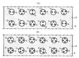
- the plurality of via conductors 8 that individually connect the plurality of back surface pads 7 formed on the back surface 4 of the substrate body 2 are four each.
- the center of each of the four via conductors 8 is located at each corner of the square in plan view.
- four via conductors 8 that individually connect between the inner layer pads 6 and between the inner layer pad 6 and the back surface pad 7 are provided along the inner layer surface 9.
- the arrangement of four via conductors 8 connected to each adjacent pad 6 among the plurality of adjacent pads 6 in the planar (vertical / horizontal) direction is either in the rotational direction in plan view. With reference to the arrangement of the four via conductors 8 in one pad 6, the arrangement of the four via conductors 8 connected to the reference pad 6 and the adjacent pad 6 is shifted by 45 degrees. *
- the four via conductors 8 that connect the pads 6 to each other are adjacent to each other in the plane (vertical / lateral) direction along the inner layer surface 9 as shown in FIG.
- the arrangement of four via conductors 8 connected to each of the pads 6 and 7 is 30 degrees with respect to the four via conductors 8 in any one back pad 7 in the rotational direction in plan view. Or it is good also as a form shifted by 45 degree
- any one of the four via conductors 8 connected to each of the plurality of pads 6 has a vertical, horizontal, and diagonal orientation in plan view. Are arranged so that they are difficult to align in a straight line.
- four via conductors connected to one pad 6 among a plurality of adjacent pads 6 are a plurality of via conductors 8 connected to each pad 6, and also one via group. *
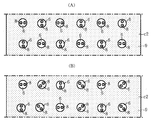
- FIG. 5A shows two via conductors 8 and three vias between a pair of upper and lower inner layer pads 6 sandwiching the ceramic layer c3 on the middle layer side in the substrate body 2 from above and below.
- the conductors 8 are alternately arranged along the plane (vertical / lateral) direction of the inner layer surface 9, and two or three via conductors 8 connected to the adjacent inner layer pads 6 are linear with each other. Shows a configuration that is difficult to align. That is, as shown in FIG. 5A, the two via conductors 8 connected to every other inner layer pad 6 in the left-right direction in the drawing are shifted from each other by 90 degrees in the rotational direction in plan view. In the upper and lower two rows shown in FIG. On the other hand, as shown in FIG.
- the three via conductors 8 connected to every other inner layer pad 6 in the left-right direction in the drawing are the same in the upper and lower rows, but In these two rows, they are shifted one by one in the oblique direction, and shifted by 180 degrees from each other in the rotation direction in plan view. *
- FIG. 5B shows three via conductors 8 and four each between a pair of upper and lower inner layer pads 6 that sandwich the lower ceramic layer c4 of the substrate body 2 from above and below.
- the via conductors 8 are alternately arranged along the plane (vertical / lateral) direction of the inner layer surface 9, and three or four via conductors 8 connected to the adjacent inner layer pads 6 are mutually connected.
- positioning difficult to align linearly is shown. That is, as shown in FIG. 5B, the three via conductors 8 connected to every other inner layer pad 6 in the horizontal direction in the drawing are shifted from each other by 180 degrees in the rotation direction in plan view.
- the upper and lower two rows shown in the figure are shifted one by one in the oblique direction, and are shifted by 30 degrees from each other in the rotational direction in plan view.
- the four via conductors 8 connected to every other inner layer pad 6 in the left-right direction are the same in each of the upper and lower two rows, but the upper and lower two rows. Another is shifted one by one in the diagonal direction.
- FIG. 6A is a partially enlarged vertical sectional view showing a further different form in the wiring board 1 shown in FIG.
- the middle ceramic layer c3 and the lower ceramic layer c4 in the substrate body 2 are separated from each other by a pair of upper and lower inner layer pads 6 sandwiching them adjacent to each other. Every four via conductors 8 are arranged.
- the four via conductors 8 that penetrate the middle ceramic layer c3 and the four via conductors 8 that penetrate the lower ceramic layer c4 are arranged. Are shifted from each other by 45 degrees in the rotation direction in plan view. *
- FIG. 6 (A) a pair of upper and lower inner layers 6 sandwiching the ceramic layer c3 on the middle layer side and the ceramic layer c4 on the lower layer side in the substrate body 2 adjacent to each other.
- three or four via conductors 8 are arranged between each other.
- the arrangement of the plurality of via conductors 8 includes three via conductors 8 penetrating the middle ceramic layer c3 and the lower ceramic layer.
- the four via conductors 8 penetrating the layer c4 are not continuous linearly in the thickness (vertical) direction of the substrate body 2.
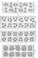
- FIG. 7A is a partial horizontal cross-sectional view similar to the above, showing different types of pads 6a and the arrangement of two via conductors 8 each using the pads 6a.
- a plurality of pads 6a having an oval shape in plan view along the plane direction of a pair of inner layer surfaces 9 sandwiching any ceramic layer cx (c1 to c5) in the substrate body 2 from above and below, The long axis is arranged so that the rotation angle is alternately shifted by 90 degrees about the centroid of the pad 6a in plan view, and between the pair of upper and lower pads 6a facing each other with the ceramic layer cx interposed therebetween, 2
- the two via conductors 8 are arranged on both ends in the major axis direction of each pad 6a.
- the plurality of pads 6a are alternately shifted by 90 degrees in the rotation direction in plan view along the plane direction of the inner layer surface 9, and two pads 6a are connected individually at both ends thereof.
- the via conductors 8 can also be more reliably prevented from generating cracks in the substrate body 2 by alternately shifting the rotation angle by 90 degrees in the rotation direction in plan view.
- FIG. 7B is a partial horizontal cross-sectional view similar to the above, showing still another form of pad 6b and the arrangement of three via conductors 8 each using the pad 6b.
- a plurality of pads 6b whose outer shape in plan view is an equilateral triangle shape along the plane direction of the pair of inner layer surfaces 9 sandwiching any ceramic layer cx from above and below in the substrate body 2 are the pads in plan view.
- the rotation angle is alternately shifted by 30 degrees or 90 degrees with the centroid of 6b as the center of rotation, and between each of the pair of upper and lower pads 6b facing each other with the ceramic layer cx in between, three each Via conductors 8 are arranged for each corner side of each pad 6b.
- the plurality of pads 6b are alternately shifted by 30 degrees or 90 degrees in the rotation direction in plan view along the plane direction of the inner layer surface 9, and individually for each corner.
- the generation of cracks in the substrate body 2 can be more reliably prevented. It becomes possible to do.
- FIG. 7C is a partial horizontal cross-sectional view similar to the above, showing different types of pads 6c and the arrangement of four via conductors 8 each using the pads 6c.
- a plurality of pads 6c having a square outer shape in plan view along the plane direction of a pair of inner layer surfaces 9 sandwiching any ceramic layer cx from above and below in the substrate body 2, and these pads 6c in plan view.
- the four via conductors 8 are arranged between the pair of upper and lower pads 6c facing each other across the ceramic layer cx. It is located for every corner side. 8
- the plurality of pads 6c are alternately shifted by 45 degrees along the plane direction of the inner layer surface 9 in the rotation direction in plan view, and are individually connected for each corner side.
- the four via conductors 8 can also be more reliably prevented from generating cracks in the substrate body 2 by alternately shifting the rotation angle by 45 degrees in the rotation direction in plan view. *
- FIG. 7D is a partial horizontal cross-sectional view similar to the above, showing yet another form of pad 6d and the arrangement of seven via conductors 8 each using the pad 6d.
- a plurality of pads 6d whose outer shape in plan view is a regular hexagonal shape along a plane direction of a pair of inner layer surfaces 9 sandwiching any ceramic layer cx in the substrate body 2 from above and below, are the pads in plan view.
- the rotation angle is alternately shifted by 30 degrees with the centroid of 6d as the rotation center, and seven via conductors 8 are arranged between the pair of upper and lower pads 6d facing each other with the ceramic layer cx interposed therebetween.
- Each corner is individually arranged at each corner and at the center.
- the plurality of pads 6d are alternately shifted by 30 degrees in the rotation direction in plan view along the plane direction of the inner layer surface 9, and are individually provided for each of these corner sides and the center portion.
- the seven via conductors 8 connected to are alternately shifted in the rotation direction in the plan view by 30 degrees, thereby making it possible to more reliably prevent the occurrence of cracks in the substrate body 2.
- the total number of via conductors 8 connected to each pad 6d may be six connected to each corner side except for the central part of each pad 6d. *
- the insulating layer constituting the substrate body is not limited to alumina, but is made of a high-temperature fired ceramic such as mullite or aluminum nitride, a low-temperature fired ceramic such as glass-ceramic, or a resin such as an epoxy-based resin. There may be.
- the insulating layer is made of low-temperature fired ceramic or resin, copper or silver is mainly used as the material for the conductors such as the pads 5 to 7 and the via conductors 8.
- the insulating layer constituting the substrate body is composed of a single layer, for example, may constitute a relay substrate, or may be a form in which any two or more insulating layers are laminated. good.
- a resin insulating layer may be laminated in any number of layers on one side or both sides of a ceramic core substrate (insulating layer). *
- an inner layer wiring having an arbitrary pattern is formed at a position other than the portion where the inner layer pad 6 is disposed, and the inner layer wiring and the pad 6 are connected to each other. It is good also as the form connected electrically.
- the substrate body 2 may have a cavity that opens toward the center of the surface 3 in plan view, and a plurality of the surface pads 5 are formed on the bottom surface of the cavity.
- the outer shape of the inner layer pad 6 is a form exhibiting a regular pentagon or a regular heptagon or more regular polygon or a deformed polygon in plan view, and a plurality of via conductors 8 at least at each corner side. May be connected individually. Or it is good also as a form which exhibits a cross shape or a star shape by planar view, and the form which connected the several via conductor 8 at least for each of these each edge part side or each corner
- the front surface pad 5 and the back surface pad 7 are each a plurality of via conductors 8 connected in parallel for each of two (or more) inner layer pads 6 formed on the inner layer surface 9 of the substrate body 2. It is good also as a form which has arrangement
- the adjacent pads 6 and 7 are shown in a grid-like arrangement in which two in the plane direction and six in the horizontal direction are arranged side by side.
- the arrangement of the plurality of adjacent pads 6 and 7 and the plurality of via conductors 8 connected to each of the pads 6 and 7 is a partial region in the substrate body 2 of the wiring board 1. Or may be provided throughout the substrate body 2. That is, in the wiring board 1 including the substrate body 2 in which a plurality of insulating layers (for example, five ceramic layers c1 to c5) are stacked, the ceramic layers c1 and c2 that are two layers on the surface 3 side are individually penetrated.
- the plurality of via conductors 8 penetrating any one of the insulating layers may be configured as described above.
- a plurality of via conductors 8 according to any of the above-described forms may be arranged only in any part of the wiring board 1 in plan view.
- the stress relaxation viewpoint and productivity are that the material, the volume, or the number of the via conductors 8 connected to each of the plurality of pads 6 and 7 arranged in a grid pattern in plan view are the same. It is preferable from the viewpoint.
- the plurality of pads 6 and 7 are arranged in a staggered position in plan view within a range not departing from the gist of the present invention, and a plurality of via conductors 8 are connected to each pad 6 and 7. It is also good.
Landscapes
- Engineering & Computer Science (AREA)
- Microelectronics & Electronic Packaging (AREA)
- Production Of Multi-Layered Print Wiring Board (AREA)
Abstract
絶縁層を挟んで対抗する複数のパッドごと間に複数本のビア導体を並列に配置しても、かかる複数本のビア導体の配列に起因して絶縁層にクラックが生じ難い配線基板、およびその製造方法を提供する。複数の絶縁層c1~c5からなり、且つ対向する表面3および裏面4を有する基板本体2と、該基板本体2の表面3、裏面4、および内層面9の少なくとも何れかの面に形成された複数のパッド5~7と、基板本体2における複数のパッド5~7ごとに接続され、且つ基板本体2の厚みに沿って並列に形成された複数のビア導体8と、を備え、基板本体2において、平面視で同一の上記面3,4,9上において隣接する複数のパッド5~7には、それぞれ複数本のビア導体8が接続され、複数本のビア導体8の配置は、平面視で同一の上記面3,4,9上で隣接するパッド5~7同士の間において互いに相違している、配線基板1。
Description
本発明は、単層あるいは複数の絶縁層を積層してなる基板本体の厚み方向に沿って、上層側のパッドと下層側のパッドとの間を複数のビア導体によって接続している配線基板に関する。
例えば、配線パターンが個別に形成された複数の絶縁層を積層してなる多層絶縁基板と、該多層絶縁基板に形成され、且つ互いに異なる層に形成された上記配線パターン同士を直列連結する複数のビア電極とを含み、1つのビア電極は、並列する複数本の単位ビア(ビア導体)で構成されるビア束からなり、上記多層絶縁基板の厚み方向に沿って隣接する複数のビア電極は、互いに複数本の単位ビアで構成されるビア束の平面視における配列を相違させた多層回路基板およびその製造方法が提案されている(例えば、特許文献1参照)。 前記多層回路基板とその製造方法によれば、前記多層絶縁基板の層間における短絡不良や、配線パターンとビア電極との短絡不良が改善され、微細なサイズのビア電極間の電気的特性を高めた多層回路基板が提供可能となる。
ところで、前記多層回路基板のように、上下一対のパッド間に挟まれた絶縁層に対して平面視で格子状に複数のパッドを配列した場合、同じ絶縁層における平面方向に沿って、隣接するパッド間に配列された複数本ずつのビア導体の何れか1本あるいは複数本が、平面視で直線状に整列してしまう場合がある。このように直線状に整列した複数本のビア導体は、絶縁層との熱膨張係数の相違に起因して応力が発生すると、かかる応力が直線状に整列した複数本のビア導体に沿って集中するため、これらのビア導体に沿って上記絶縁層に平面方向に沿ったクラックが発生する場合があった。
本発明は、背景技術で説明した問題点を解決し、絶縁層を挟んで対向する複数対のパッドごと間に複数本のビア導体を並列に配置しても、かかる複数本のビア導体の配列に起因して絶縁層にクラックが生じ難い配線基板、およびその製造方法を提供する、ことを課題とする。
本発明は、前記課題を解決するため、絶縁層を挟んで対向する複数のパッドごと間に複数本ずつのビア導体を並列に配置するに際し、平面視で互いに隣接するパッド間ごとにおける複数本ずつのビア導体の配置を相違させる、ことに着想して成されたものである。 即ち、本発明の配線基板(請求項1)は、単数あるいは複数の絶縁層からなり、且つ対向する表面および裏面を有する基板本体と、該基板本体の表面、裏面、および内層面の少なくとも何れかの面に形成された複数のパッドと、上記基板本体における上記複数のパッドごとに接続され、且つ上記基板本体の厚みに沿って並列に形成された複数のビア導体と、を備えた配線基板であって、上記基板本体において、平面視で同一の上記面上において隣接する上記複数のパッドには、それぞれ複数本のビア導体が接続されており、該複数本のビア導体の配置は、平面視で同一の上記面上で隣接するパッド同士の間において互いに相違している、ことを特徴とする。
前記のような配線基板によれば、以下の効果(1)を奏することができる。(1)前記複数のパッドには、それぞれ複数本のビア導体(即ち、ビア群)が接続され、該複数本のビア導体の配置(即ち、1つのパッドに対して複数本のビア導体が配置されている位置)が、平面視で同一の前記表面、裏面、あるいは内層面上で隣接するパッド同士の間において互いに相違している。そのため、前記何れかの面に沿って隣接するパッドごとに接続された複数本ずつのビア導体は、平面視で直線状に整列しにくくなるので、絶縁層との熱膨張係数の差による応力を生じても、該応力により前記基板にクラックが発生する事態を抑制できる。従って、形状および寸法精度が高いと共に、電気的特性が安定した配線基板にできる。
尚、前記絶縁層は、例えば、アルミナなどのセラミック、あるいはエポキシ系などの樹脂からなる。 また、前記パッドは、前記基板本体の厚み方向で隣接する絶縁層ごとに形成された複数本ずつのビア導体同士の間に挟まれるビアカバーを含んでいる。 更に、前記パッドは、前記基板本体の表面における表面パッド、あるいは前記基板本体の裏面における裏面パッドともなる。 また、前記パッドは、複数の絶縁層の層間に形成され、且つ平面視で所要パターンを呈する内層配線の一部に形成されていても良い。 更に、前記パッドは、平面視で円形状、正方形状、三角形状、六角形状、あるいは星形状などを呈する。 また、前記内層面は、上下に隣接する絶縁層同士の間を区分する層間である。 更に、前記「配置」は、所定の配列模様(パターン)を含むものである。 加えて、前記複数本のビア導体が前記基板本体の表面側と裏面側とのパッド間に並列に形成する導電路は、主に電源用あるいは接地用電流の通電に活用される。
また、本発明には、前記複数のパッドのそれぞれに接続される前記複数本のビア導体は、2本のビア導体からなり、平面視で同一の前記面上で互いに隣接する上記複数のパッドに接続する上記複数本のビア導体は、平面視における回転方向において、上記隣接する複数のパッドのうちの1つのパッドにおける上記複数本のビア導体の配置を基準として、少なくとも30度以上ずれて配置されている、配線基板(請求項2)も含まれる。 これによれば、前記何れかの面に沿って隣接するパッドごとに接続された2本ずつのビア導体からなる複数本のビア導体の配置は、互いに平面視で直線状に整列しにくくなるので、前記効果(1)を確実に奏することが可能となる。 尚、前記回転方向のずれを30度以上としたのは、該ずれが30度未満では、複数本ずつのビア導体(ビア群)の何れかが、平面視で直線状に整列し易くなる故である。 また、前記表面側のパッドと裏面側のパッドとの間を接続する複数本のビア導体が2本のビア導体の群である場合、平面視で隣接し合う2本ずつのビア導体の組は、例えば、互いに45度ずつ、あるいは90度ずつずれている。
更に、本発明には、前記複数のパッドのそれぞれに接続される前記複数本のビア導体は、3本以上のビア導体からなり、前記複数本のビア導体は、平面視で正三角形以上の正多角形の角部側に個別に配置されており、平面視で同一の前記面上において互いに隣接する上記複数のパッドに接続する上記複数本のビア導体は、平面視における回転方向において、上記隣接する複数のパッドのうちの1つのパッドにおける上記複数本のビア導体の配置を基準として、少なくとも30度以上ずれて配置されている、配線基板(請求項3)も含まれる。 これによれば、前記何れかの面に沿って隣接するパッドごとに接続された3本以上ずつのビア導体からなる複数本のビア導体の配置は、互いに平面視で直線状に整列しにくくなるので、前記効果(1)を確実に奏することが可能となる。
尚、回転方向のずれを30度以上とした理由は、前記と同様の理由による。 また、前記表面側のパッドごとと裏面側のパッドごととの間を接続する複数本のビア導体が3本のビア導体の群で且つ平面視で正三角形の角部側(即ち、正多角形の角部付近ごとの位置)に形成されている場合、平面視で隣接し合う3本ずつのビア導体の組(複数本のビア導体の組)は、例えば、互いに60度ずつずれている。 更に、前記表面側のパッドと裏面側のパッドとの間を接続する複数のビア導体が4本のビア導体の群で、且つ平面視で正方形の角部側ごとに形成されている場合、平面視で隣接し合う4本ずつのビア導体の組は、例えば、互いに45度ずつずれている。 加えて、上述した「回転方向のずれ」とは、前記パッドの図心を回転中心として、回転角が30度以上発生している状態を指している。
また、本発明には、前記複数のパッドにおける平面視で同一の前記面上で互いに隣接する前記パッド同士にそれぞれ接続されている前記複数本のビア導体の数は、互いに異なっている、配線基板(請求項4)も含まれる。 これによれば、前記面上で互いに隣接する前記パッド同士に接続されている複数本のビア導体同士の数が互いに異なっているので、前記内層面の平面方向に沿って、複数本のビア導体が直線状に整列する事態を容易に阻止できる。従って、前記効果(1)をより確実に得ることが可能となる。
更に、本発明には、前記基板本体は、複数の絶縁層からなり、前記表面側と裏面側との厚み方向において隣接する上下2層以上の絶縁層の層間ごとにおける前記内層面上に、前記パッドが複数個形成され、上層側の絶縁層を貫通し、前記パッドごとに接続される複数本のビア導体と、下層側の絶縁層を貫通し、前記パッドごとに接続される前記複数本のビア導体との平面視おける配置が互いに相違している、配線基板(請求項5)も含まれる。 これによれば、前記効果(1)に加えて、以下の効果(2)が更に得られる。(2)前記基板本体の厚み方向において隣接する上下2層以上の絶縁層の層間ごとにおける前記内層面上に、前記パッドが複数個形成され、上層側の絶縁層を貫通し、前記パッドごとに接続される複数本のビア導体と、下層側の絶縁層を貫通し、前記パッドごとに接続される複数本のビア導体との平面視おける配置が互いに相違している。そのため、上記基板本体の厚み方向に沿って隣接するパッドごとに接続された複数本のビア導体も、平面視で直線状に整列しにくくなるので、上記内層面に沿った平面方向および基板本体の厚み方向の双方に沿ってクラックが発生しにくくなる。従って、形状および寸法精度が一層高く、且つ電気的特性が更に安定した配線基板とすることができる。
加えて、本発明には、前記上層側の絶縁層を貫通する前記複数本のビア導体の数と、下層側の絶縁層を貫通する前記複本数のビア導体の数とが、互いに相違している、配線基板(請求項6)も含まれる。 これによれば、前記基板本体の厚み方向において隣接する上下2層以上の絶縁層の層間ごとにおける前記内層面上に、前記パッドが複数個形成され、該パッドごとを挟んだ上層側の絶縁層を貫通し、前記パッドごとに接続される複数本のビア導体の数と、下層側の絶縁層を貫通し、前記パッドごとに接続される複数本のビア導体の数とが互いに相違している。従って、前記効果(2)を容易に得ることが可能となる。
以下において、本発明を実施するための形態について説明する。 図1は、本発明による一形態の配線基板1を示す垂直断面図である。 かかる配線基板1は、図1に示すように、複数のセラミック層(絶縁層)c1~c5を積層してなり、対向する表面3および裏面4を有する基板本体2と、該基板本体2の表面3、裏面4、および複数の内層面9ごとに個別に且つ平面視で縦横に格子状に形成された複数ずつの表面パッド
5、裏面パッド7、および内層パッド6と、上記基板本体2の厚み方向に沿って隣接する表面パッド5と内層パッド6との間、内層パッド6同士の間、および内層パッド6と裏面パッド7との間を個別に接続する複数本ずつのビア導体8と、を備えている。 尚、前記セラミック層c1~c5は、例えば、アルミナからなり、前記パッド5~7やビア導体8は、主にタングステン(以下、単にWと称する)あるいはモリブデン(以下、単にMoと称する)からなる。また、内層パッド6は、平面視で円形状を呈し、表面パッド5および裏面パッド7は、平面視で円形状のほか、例えば、矩形(正方形または長方形)状などの任意の形状を呈していても良い。
5、裏面パッド7、および内層パッド6と、上記基板本体2の厚み方向に沿って隣接する表面パッド5と内層パッド6との間、内層パッド6同士の間、および内層パッド6と裏面パッド7との間を個別に接続する複数本ずつのビア導体8と、を備えている。 尚、前記セラミック層c1~c5は、例えば、アルミナからなり、前記パッド5~7やビア導体8は、主にタングステン(以下、単にWと称する)あるいはモリブデン(以下、単にMoと称する)からなる。また、内層パッド6は、平面視で円形状を呈し、表面パッド5および裏面パッド7は、平面視で円形状のほか、例えば、矩形(正方形または長方形)状などの任意の形状を呈していても良い。
図1に示すように、前記基板本体2において、上層側のセラミック層c1,c2を個別に貫通し、該基板本体2の表面3とこれの下方に隣接する内層面9とに形成された前記パッド5,6間ごと、あるいは、セラミック層c1,c2間とセラミック層c2,c3間との内層面9同士の間に形成された内層パッド6同士間ごとを接続する複数本のビア導体8は、2本ずつである。 例えば、セラミック層c1,c2間およびセラミック層c2,c3間の内層面9同士の間に形成された内層パッド6同士間ごとを接続する2本ずつのビア導体8は、図2(A)に示すように、上記内層面9に沿った平面(縦・横・斜め方向)方向において、互いに隣接するパッド6ごとに接続された2本ずつのビア導体8の配置は、平面視における回転方向において、隣接する複数のパッド6のうちの何れか1つの上記パッド6における2本のビア導体8の配置を基準として、基準としたパッド6と隣のパッド6とに接続される2本のビア導体8の配置が90度ずつずれている。その結果、上記複数のパッド6ごとに接続される2本ずつのビア導体8の何れかが、平面視で縦・横・斜めの全方向において、直線状に整列していない。かかる形態では、隣接する複数のパッド6のうち、1つのパッド6に接続する2本のビア導体が、パッド6ごとに接続する複数本のビア導体8であり、1つのビア群でもある。
更に、前記パッド6同士間ごとを接続する2本ずつのビア導体8について、図2(B)に示すように、前記内層面9に沿った平面方向において、互いに隣接するパッド6ごとに接続された2本ずつのビア導体8の配置は、平面視における回転方向において、隣接する複数のパッド6のうちの何れか1つのパッド6における2本のビア導体8の配置を基準として、基準としたパッド6と隣のパッド6とに接続される2本のビア導体8の配置を45度ずつ、あるいは90度ずつずらした形態としても良い。その結果、上記複数のパッド6ごとに接続される2本ずつのビア導体8の何れかが、平面視で縦・横・斜めの全方向において、直線状に整列していない。 加えて、図1の上方に示すように、セラミック層c1,c2を個別に貫通して隣接する2本ずつのビア導体8も、平面視で互いに90度ずつずれている。
図1に示すように、前記基板本体2において、中層側のセラミック層c3を個貫通し、該セラミック層c3を挟んで上下に隣接する内層パッド6同士の間ごとには、例えば、それぞれ3本(複数本)ずつのビア導体8が接続されている。該3本ずつのビア導体8は、平面視で正三角形(仮想)の各角部に、それぞれの中心が位置している。 即ち、中層側のセラミック層c3を挟む上下一対の内層面9同士に形成された内層パッド6同士間ごとを接続する3本ずつのビア導体8は、図3(A)に示すように、上記内層面9に沿った平面(縦・横方向)方向において、互いに隣接するパッド6ごとに接続された3本ずつのビア導体8の配置は、平面視における回転方向において、何れか1つのパッド6における3本のビア導体8を基準として、30度ずつずれている。かかる形態では、隣接する複数のパッド6のうち、1つのパッド6に接続する3本のビア導体が、パッド6ごとに接続する複数本のビア導体8であり、1つのビア群でもある。
更に、前記パッド6同士間ごとを接続する3本ずつのビア導体8は、図3(B)に示すように、上記内層面6に沿った平面方向において、互いに隣接するパッド6ごとに接続された3本ずつのビア導体8の配置は、平面視における回転方向において、隣接する複数のパッド6のうちの何れか1つのパッド6における3本のビア導体8の配置を基準として、基準としたパッド6と隣のパッド6とに接続される3本のビア導体8の配置を180度ずつずらした形態としても良い。 その結果、図3(A),(B)に示すように、上記複数のパッド6ごとに接続される3本ずつのビア導体8の何れかが、平面視で縦・横・斜めの全方向において、直線状に整列しにくいように配置されている。
図1の下方に示すように、前記基板本体2において、下層側のセラミック層c4,c5を個別に貫通し、セラミック層c3,c4間の内層面9に形成された複数の内層パッド6と、該基板本体2の裏面4に形成された複数の裏面パッド7との間を個別に接続する複数本のビア導体8は、それぞれ4本ずつである。該4本ずつのビア導体8は、平面視で正方形の各角部にそれぞれの中心が位置している。 上記内層パッド6同士の間ごと、および内層パッド6と裏面パッド7との間ごとを個別に接続する4本ずつのビア導体8は、図4(A)に示すように、内層面9に沿った平面(縦・横方向)方向において、隣接する複数のパッド6のうちの互いに隣接するパッド6ごとに接続された4本ずつのビア導体8の配置は、平面視における回転方向において、何れか1つのパッド6における4本のビア導体8の配置を基準として、基準としたパッド6と隣のパッド6とに接続される4本のビア導体8の配置が45度ずつずれている。
更に、上記パッド6同士間などを接続する4本ずつのビア導体8は、図4(B)に示すように、上記内層面9に沿った平面(縦・横方向)方向において、互いに隣接する前記パッド6,7ごとに接続された4本ずつのビア導体8の配置は、平面視における回転方向において、何れか1つの裏面パッド7における4本のビア導体8を基準として、30度ずつ、あるいは45度ずつずらした形態としても良い。 その結果、図4(A),(B)に示すように、上記複数のパッド6ごとに接続される4本ずつのビア導体8の何れかが、平面視で縦・横・斜めの全方向において、直線状に整列しにくいように配置されている。かかる形態では、隣接する複数のパッド6のうち、1つのパッド6に接続する4本のビア導体が、パッド6ごとに接続する複数本のビア導体8であり、1つのビア群でもある。
図5(A)は、前記基板本体2における中層側のセラミック層c3を上下から隣接して挟む上下一対の内層パッド6同士の間に、2本ずつのビア導体8と、3本ずつのビア導体8とを前記内層面9の平面(縦・横)方向に沿って、交互に配置すると共に、互いに隣接する内層パッド6同士に接続される2本あるいは3本のビア導体8が互いに直線状に整列しにくい配置とした形態を示す。 即ち、図5(A)に示すように、図示で左右方向に1つ置きの内層パッド6に接続される2本ずつのビア導体8は、平面視の回転方向で互いに90度ずつずれており、且つ図示の上下2列では斜め方向に1つずつずれて配列されている。 一方、図5(A)に示すように、図示で左右方向に1つ置きの内層パッド6に接続される3本ずつのビア導体8は、上下2列内ごとでは同じ配置であるが、上下の2列では、斜め方向に1つずつずれていると共に、平面視の回転方向で互いに180度ずつずれている。
また、図5(B)は、前記基板本体2における下層側のセラミック層c4を上下から隣接して挟む上下一対の内層パッド6同士の間に、3本ずつのビア導体8と、4本ずつのビア導体8とを前記内層面9の平面(縦・横)方向に沿って、交互に配置すると共に、互いに隣接する内層パッド6同士に接続される3本または4本のビア導体8が互いに直線状に整列しにくい配置とした形態を示す。 即ち、図5(B)に示すように、図示で左右方向に1つ置きの内層パッド6に接続される3本ずつのビア導体8は、平面視の回転方向で互いに180度ずつずれており、且つ図示の上下2列では斜め方向に1つずつずれていると共に、平面視の回転方向で互いに30度ずつずれている。 一方、図5(B)に示すように、左右方向で1つ置きの内層パッド6に接続される4本ずつのビア導体8は、上下2列内ごとでは同じ配置であるが、上下2列別では、斜め方向に1つずつずれている。 以上のように、前記内層面9などに沿った平面方向において、互いに隣接する内層パッド6などの接続される複数本ずつのビア導体8の配置が相違している配線基板1によれば、前記効果(1)を得られることが容易に理解される。
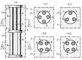
図6(A)は、前記図1で示した配線基板1において、更に異なる形態を示す部分拡大垂直断面図である。 図6(A)に示すように、前記基板本体2における中層側のセラミック層c3と、下層側のセラミック層c4とには、これらを個別に隣接して挟む上下一対ずつの内層パッド6同士間ごとに、同じ4本ずつのビア導体8が配置されている。それらの配置は、図6(X1),(X2)に示すように、中層側のセラミック層c3を貫通する4本のビア導体8と、下層側のセラミック層c4を貫通する4つのビア導体8とは、平面視の回転方向で互いに45度ずつずれている。
一方、図6(A)に示すように、前記基板本体2における中層側のセラミック層c3と、下層側のセラミック層c4とには、これらを個別に隣接して挟む上下一対ずつの内層パッド6同士の間ごとに、3本ずつ、あるいは4本ずつのビア導体8が配置されているとする。この場合、これらの複数本のビア導体8の配置は、図6(Y1),(Y2)に示すように、中層側のセラミック層c3を貫通する3本のビア導体8と、下層側のセラミック層c4を貫通する4本のビア導体8とは、前記基板本体2の厚み(垂直)方向において、直線状に連続していない。 以上のように、前記基板本体2の厚み方向に沿って、個々のセラミック層cxを個別に貫通する複数本ずつのビア導体8を、上記厚み方向に沿って直線状に整列させない形態を更に加えることにより、前記配線基板1に対して前記効果(2)も追加することが可能となる。
図7(A)は、異なる形態のパッド6aと、これを用いた2本ずつのビア導体8の配置とを示す前記同様の部分水平断面図である。 前記基板本体2における何れかのセラミック層cx(c1~c5)を上下から挟む一対の内層面9の平面方向に沿って、平面視の外形が長円形状である複数のパッド6aを、それらの長軸が平面視で該パッド6aの図心を回転中心として交互に回転角度が90度ずつずれるように配置すると共に、上記セラミック層cxを挟んで対向する上下一対のパッド6a同士間に、2本のビア導体8を各パッド6aの長軸方向の両端側に配置したものである。 以上のように、複数のパッド6aを、内層面9の平面方向に沿って、平面視の回転方向で交互に回転角度を90度ずつずらすと共に、これらの両端ごとに個別に接続される2本のビア導体8も平面視の回転方向で交互に回転角度を90度ずつずらすことで、前記基板本体2の内部におけるクラックの発生を一層確実に阻止することが可能となる。
図7(B)は、更に異なる形態のパッド6bと、これを用いた3本ずつのビア導体8の配置とを示す前記同様の部分水平断面図である。 前記基板本体2における何れかのセラミック層cxを上下から挟む一対の内層面9の平面方向に沿って、平面視の外形が正三角形状である複数のパッド6bを、それらが平面視で該パッド6bの図心を回転中心として交互に回転角度が30度ずつ、あるいは90度ずつずれるように配置すると共に、上記セラミック層cxを挟んで対向する上下一対のパッド6b同士間に、3本ずつのビア導体8を各パッド6bの角部側ごとに配置したものである。 以上のように、複数のパッド6bを、内層面9の平面方向に沿って、平面視の回転方向で交互に回転角度を30度ずつ、あるいは90度ずつずらし、且
つこれらの角部ごとに個別に接続される3本のビア導体8を、平面視の回転方向で交互に回転角度を30度ずつ、あるいは90度ずつずらすことで、前記基板本体2の内部におけるクラックの発生をより確実に阻止することが可能となる。
つこれらの角部ごとに個別に接続される3本のビア導体8を、平面視の回転方向で交互に回転角度を30度ずつ、あるいは90度ずつずらすことで、前記基板本体2の内部におけるクラックの発生をより確実に阻止することが可能となる。
図7(C)は、別異な形態のパッド6cと、これを用いた4本ずつのビア導体8の配置とを示す前記同様の部分水平断面図である。 前記基板本体2における何れかのセラミック層cxを上下から挟む一対の内層面9の平面方向に沿って、平面視の外形が正方形状である複数のパッド6cを、それらが平面視で該パッド6cの図心を回転中心として交互に回転角度が45度ずつずれるように配置すると共に、上記セラミック層cxを挟んで対向する上下一対のパッド6c同士間に、4本のビア導体8を各パッド6cの角部側ごとに位置したものである。8 以上のように、複数のパッド6cを、内層面9の平面方向に沿って、平面視の回転方向で交互に回転角度を45度ずつずらし、且つこれらの角部側ごとに個別に接続される4本のビア導体8も平面視の回転方向で交互に回転角度を45度ずつずらすことによって、前記基板本体2の内部におけるクラックの発生を一層確実に阻止することが可能となる。
図7(D)は、更に別形態のパッド6dと、これを用いた7本ずつのビア導体8の配置とを示す前記同様の部分水平断面図である。 前記基板本体2における何れかのセラミック層cxを上下から挟む一対の内層面9の平面方向に沿って、平面視の外形が正六方形状である複数のパッド6dを、それらが平面視で該パッド6dの図心を回転中心として交互に回転角度が30度ずつずれるように配置すると共に、上記セラミック層cxを挟んで対向する上下一対のパッド6d同士間に、7本のビア導体8をパッド6dごとの各角部側ごと、および中心部に個別に配置したものである。 以上のように、複数のパッド6dを、内層面9の平面方向に沿って、平面視の回転方向で交互に回転角度を30度ずつずらし、且つこれらの角部側ごとと中心部とに個別に接続される7本のビア導体8も平面視の回転方向で交互に回転角度を30度ずつずらすことによって、前記基板本体2の内部におけるクラックの発生を一層確実に阻止することが可能となる。 尚、上記パッド6dごとに接続するビア導体8の総数は、前記パッド6dごとの中心部を除いて、各角部側ごとに接続する6本ずつの形態としても良い。
本発明は、以上において説明した各形態に限定されるものではない。 例えば、前記基板本体を構成する絶縁層は、前記アルミナに限らず、ムライトや窒化アルミニウムなどの高温焼成セラミック、ガラス-セラミックなどの低温焼成セラミック、あるいは、例えば、エポキシ系などの樹脂からなるものであっても良い。上記絶縁層が低温焼成セラミックや樹脂からなる場合、前記パッド5~7やビア導体8などの導体の材料には、主に銅あるいは銀が用いられる。 また、前記基板本体を構成する絶縁層は、単層からなるものとし、例えば、中継基板を構成しても良いし、あるいは、2層以上である何れか複数の絶縁層を積層した形態としても良い。この場合、例えば、セラミックからなるコア基板(絶縁層)の片面あるいは両面に樹脂の絶縁層を任意の層数で積層しても良い。
更に、前記セラミック層cx同士の層間である前記内層面9には、前記内層パッド6が配置された部位以外の位置に、任意パターンの内層配線を形成し、該内層配線と上記パッド6とを電気的に接続させた形態としても良い。 また、前記基板本体2は、平面視で前記表面3の中央側に開口するキャビティを有し、且つ該キャビティの底面に複数の前記表面パッド5が形成されている形態としても良い。
更に、前記内層パッド6の外形は、平面視で正五角形あるいは正七角形以上の正多角形やこれらの変形多角形を呈する形態とし、且つ少なくともこれらの各角部側ごとに複数本のビア導体8を個別に接続しても良い。あるいは、平面視で十字形状あるいは星形状を呈する形態とし、且つ少なくともこれらの各端部側あるいは各角部側ごとに複数本のビア導体8を個別に接続した形態としても良い。 加えて、前記表面パッド5や裏面パッド7は、前記基板本体2の内層面9に形成された2つ(複数)以上の内層パッド6ごとに並列して接続された複数本ずつのビア導体8の全てと接続できる配置を有する形態としても良い。
尚、前記の各形態では、隣接する複数のパッド6,7は、平面方向において縦に2つ横に6つが並ぶ格子状の配置で示したが、格子状に配置する数は、任意の数として良い。 また、前記の各形態で隣接する複数のパッド6,7と、該パッド6,7ごとに接続される複数本のビア導体8との配置は、配線基板1の基板本体2における一部の領域に備えていても良いし、前記基板本体2の全体にわたって備えていても良い。即ち、複数の絶縁層(例えば、5層のセラミック層c1~c5)を積層した基板本体2を備える配線基板1において、表面3側の2層であるセラミック層c1,c2を個別に貫通し、該セラミック層c1,c2間に形成された複数のパッド6と接続する複数本のビア導体8の配置のみを前述した形態としても良い。 更に、前記基板本体2における裏面4側の2層であるセラミック層c4,c5を個別に貫通し、該セラミック層c4,c5間に形成された複数のパッド6と接続する複数本のビア導体8の配置のみを前述した形態としても良い。
更に、各絶縁層(例えば、5層のセラミック層c1~c5)のうちの何れか1層を貫通する複数本のビア導体8の配置のみを、前述した形態としても良い。 また、配線基板1の平面視における何れか一部の領域のみに、前述した何れかの形態による複数本のビア導体8の配置をしても良い。 更に、平面視で格子状に配置された複数のパッド6,7ごとに接続される複数本のビア導体8の材料、体積、または本数は、同一であることが前記応力緩和の観点や生産性観点から好ましい。 加えて、複数のパッド6,7は、本発明の趣旨を逸脱しない範囲において、平面視で千鳥状の位置ごとに配置し、該パッド6,7ごとに複数本のビア導体8を接続した形態としても良い。
本発明によれば、絶縁層を挟んで対向する複数のパッドごと間に複数ずつのビア導体を並列に配置しても、かかる複数のビア導体の配列に起因して絶縁層にクラックが生じ難い配線基板、およびその製造方法を確実に提供できる。
1…………………配線基板 2…………………基板本体 3…………………表面(面) 4…………………裏面(面) 5…………………表面パッド(パッド) 6,6a~6d…内層パッド(パッド) 7…………………裏面パッド(パッド) 8…………………ビア導体 9…………………内層面(面) c1~c5………セラミック層(絶縁層)
Claims (6)
- 単数あるいは複数の絶縁層からなり、且つ対向する表面および裏面を有する基板本体と、
上記基板本体の表面、裏面、および内層面の少なくとも何れかの面に形成された複数のパッドと、
上記基板本体における上記複数のパッドごとに接続され、且つ上記基板本体の厚みに沿って並列に形成された複数のビア導体と、を備えた配線基板であって、
上記基板本体において、平面視で同一の上記面上において隣接する上記複数のパッドには、それぞれ複数本のビア導体が接続されており、
上記複数本のビア導体の配置は、平面視で同一の上記面上で隣接するパッド同士の間において互いに相違している、
ことを特徴とする配線基板。
- 前記複数のパッドのそれぞれに接続される前記複数本のビア導体は、2本のビア導体からなり、
平面視で同一の前記面上で互いに隣接する上記複数のパッドに接続する前記複数本のビア導体は、平面視における回転方向において、上記隣接する複数のパッドのうちの1つのパッドにおける上記複数本のビア導体の配置を基準として、少なくとも30度以上ずれて配置されている、
ことを特徴とする請求項1に記載の配線基板。
- 前記複数のパッドのそれぞれに接続される前記複数本のビア導体は、3本以上のビア導体からなり、
上記複数本のビア導体は、平面視で正三角形以上の正多角形の角部側に個別に配置されており、
平面視で同一の前記面上において互いに隣接する上記複数のパッドに接続する上記複数本のビア導体は、平面視における回転方向において、上記隣接する複数のパッドのうちの1つのパッドにおける上記複数本のビア導体の配置を基準として、少なくとも30度以上ずれて配置されている、
ことを特徴とする請求項1に記載の配線基板。
- 前記複数のパッドにおける平面視で同一の前記面上で互いに隣接する前記パッド同士にそれぞれ接続されている前記複数本のビア導体の数は、互いに異なっている、
ことを特徴とする請求項1または3に記載の配線基板。
- 前記基板本体は、複数の絶縁層からなり、前記表面側と裏面側との厚み方向において隣接する上下2層以上の絶縁層の層間ごとにおける前記内層面上に、前記パッドが複数個形成され、上層側の絶縁層を貫通し、前記パッドごとに接続される前記複数本のビア導体と、下層側の絶縁層を貫通し、前記パッドごとに接続される前記複数本のビア導体との平面視おける配置が互いに相違している、
ことを特徴とする請求項1乃至4の何れか一項に記載の配線基板。
- 前記上層側の絶縁層を貫通する前記複数本のビア導体の数と、下層側の絶縁層を貫通する前記複数本のビア導体の数とが、互いに相違している、
ことを特徴とする請求項5に記載の配線基板。
Priority Applications (3)
| Application Number | Priority Date | Filing Date | Title |
|---|---|---|---|
| EP18806598.1A EP3634093A4 (en) | 2017-05-24 | 2018-05-11 | CONNECTION TABLE |
| CN201880033232.3A CN110663292B (zh) | 2017-05-24 | 2018-05-11 | 布线基板 |
| US16/478,164 US10905008B2 (en) | 2017-05-24 | 2018-05-11 | Wiring board |
Applications Claiming Priority (2)
| Application Number | Priority Date | Filing Date | Title |
|---|---|---|---|
| JP2017102656A JP6730960B2 (ja) | 2017-05-24 | 2017-05-24 | 配線基板 |
| JP2017-102656 | 2017-05-24 |
Publications (1)
| Publication Number | Publication Date |
|---|---|
| WO2018216505A1 true WO2018216505A1 (ja) | 2018-11-29 |
Family
ID=64395541
Family Applications (1)
| Application Number | Title | Priority Date | Filing Date |
|---|---|---|---|
| PCT/JP2018/018291 WO2018216505A1 (ja) | 2017-05-24 | 2018-05-11 | 配線基板 |
Country Status (5)
| Country | Link |
|---|---|
| US (1) | US10905008B2 (ja) |
| EP (1) | EP3634093A4 (ja) |
| JP (1) | JP6730960B2 (ja) |
| CN (1) | CN110663292B (ja) |
| WO (1) | WO2018216505A1 (ja) |
Families Citing this family (8)
| Publication number | Priority date | Publication date | Assignee | Title |
|---|---|---|---|---|
| JP6869209B2 (ja) * | 2018-07-20 | 2021-05-12 | 日本特殊陶業株式会社 | 配線基板 |
| JP7076347B2 (ja) * | 2018-09-18 | 2022-05-27 | 日本特殊陶業株式会社 | 導波管 |
| WO2020137878A1 (ja) * | 2018-12-25 | 2020-07-02 | 京セラ株式会社 | 電子部品実装用基板および電子装置 |
| JP2020150000A (ja) * | 2019-03-11 | 2020-09-17 | 日立金属株式会社 | セラミックス基板 |
| US11596055B2 (en) * | 2019-12-27 | 2023-02-28 | Intel Corporation | Apparatus and system of a printed circuit board (PCB) including a radio frequency (RF) transition |
| US11776899B2 (en) | 2020-05-11 | 2023-10-03 | Mediatek Inc. | Via array design for multi-layer redistribution circuit structure |
| DE102022104156A1 (de) | 2022-02-22 | 2023-08-24 | Rogers Germany Gmbh | Metall-Keramik-Substrat und Verfahren zur Herstellung eines Metall-Keramik-Substrats |
| JP7448060B1 (ja) | 2023-03-27 | 2024-03-12 | Toto株式会社 | 静電チャック |
Citations (5)
| Publication number | Priority date | Publication date | Assignee | Title |
|---|---|---|---|---|
| JPH0423495A (ja) * | 1990-05-18 | 1992-01-27 | Nec Corp | 多層配線基板 |
| JPH06326471A (ja) * | 1993-05-17 | 1994-11-25 | Sony Corp | 多層配線基板 |
| JP2005527122A (ja) * | 2002-05-23 | 2005-09-08 | インターナショナル・ビジネス・マシーンズ・コーポレーション | 積層型ビア構造体 |
| JP2012028730A (ja) | 2010-07-21 | 2012-02-09 | Samsung Electro-Mechanics Co Ltd | 多層回路基板及び多層回路基板の製造方法 |
| WO2016052284A1 (ja) * | 2014-09-30 | 2016-04-07 | 株式会社村田製作所 | 多層基板 |
Family Cites Families (10)
| Publication number | Priority date | Publication date | Assignee | Title |
|---|---|---|---|---|
| US7215007B2 (en) * | 2003-06-09 | 2007-05-08 | Wemtec, Inc. | Circuit and method for suppression of electromagnetic coupling and switching noise in multilayer printed circuit boards |
| US7239526B1 (en) * | 2004-03-02 | 2007-07-03 | Xilinx, Inc. | Printed circuit board and method of reducing crosstalk in a printed circuit board |
| US7999192B2 (en) * | 2007-03-14 | 2011-08-16 | Amphenol Corporation | Adjacent plated through holes with staggered couplings for crosstalk reduction in high speed printed circuit boards |
| TWI356480B (en) | 2007-05-07 | 2012-01-11 | Siliconware Precision Industries Co Ltd | Semiconductor package substrate |
| JP5853351B2 (ja) * | 2010-03-25 | 2016-02-09 | ソニー株式会社 | 半導体装置、半導体装置の製造方法、及び電子機器 |
| WO2013052067A1 (en) * | 2011-10-07 | 2013-04-11 | Intel Corporation | Formation of dram capacitor among metal interconnect |
| US9269593B2 (en) * | 2012-05-29 | 2016-02-23 | Zhuhai Advanced Chip Carriers & Electronic Substrate Solutions Technologies Co. Ltd. | Multilayer electronic structure with integral stepped stacked structures |
| KR20150046615A (ko) * | 2013-10-22 | 2015-04-30 | 삼성전기주식회사 | 다층 인쇄회로기판 |
| JP2015126053A (ja) * | 2013-12-26 | 2015-07-06 | 富士通株式会社 | 配線基板、配線基板の製造方法及び電子装置 |
| JP6818534B2 (ja) | 2016-12-13 | 2021-01-20 | キヤノン株式会社 | プリント配線板、プリント回路板及び電子機器 |
-
2017
- 2017-05-24 JP JP2017102656A patent/JP6730960B2/ja active Active
-
2018
- 2018-05-11 EP EP18806598.1A patent/EP3634093A4/en active Pending
- 2018-05-11 CN CN201880033232.3A patent/CN110663292B/zh active Active
- 2018-05-11 WO PCT/JP2018/018291 patent/WO2018216505A1/ja unknown
- 2018-05-11 US US16/478,164 patent/US10905008B2/en active Active
Patent Citations (5)
| Publication number | Priority date | Publication date | Assignee | Title |
|---|---|---|---|---|
| JPH0423495A (ja) * | 1990-05-18 | 1992-01-27 | Nec Corp | 多層配線基板 |
| JPH06326471A (ja) * | 1993-05-17 | 1994-11-25 | Sony Corp | 多層配線基板 |
| JP2005527122A (ja) * | 2002-05-23 | 2005-09-08 | インターナショナル・ビジネス・マシーンズ・コーポレーション | 積層型ビア構造体 |
| JP2012028730A (ja) | 2010-07-21 | 2012-02-09 | Samsung Electro-Mechanics Co Ltd | 多層回路基板及び多層回路基板の製造方法 |
| WO2016052284A1 (ja) * | 2014-09-30 | 2016-04-07 | 株式会社村田製作所 | 多層基板 |
Non-Patent Citations (1)
| Title |
|---|
| See also references of EP3634093A4 |
Also Published As
| Publication number | Publication date |
|---|---|
| US20190373727A1 (en) | 2019-12-05 |
| CN110663292A (zh) | 2020-01-07 |
| JP2018198271A (ja) | 2018-12-13 |
| EP3634093A4 (en) | 2021-03-10 |
| EP3634093A1 (en) | 2020-04-08 |
| CN110663292B (zh) | 2022-12-16 |
| US10905008B2 (en) | 2021-01-26 |
| JP6730960B2 (ja) | 2020-07-29 |
Similar Documents
| Publication | Publication Date | Title |
|---|---|---|
| WO2018216505A1 (ja) | 配線基板 | |
| JP6869209B2 (ja) | 配線基板 | |
| TWI569482B (zh) | Method for manufacturing thermoelectric conversion device | |
| JP6528592B2 (ja) | 半導体装置 | |
| JP2013211302A (ja) | 積層コイル部品 | |
| US20120138343A1 (en) | Three dimensional interposer device, chip package and probe card contactor | |
| JP7232305B2 (ja) | ウェーハテスト用プローブカード | |
| JP2016111247A (ja) | 積層セラミックコンデンサ | |
| US10231331B2 (en) | Multilayer wiring board and probe card having the same | |
| JP2001085465A (ja) | 半導体装置 | |
| KR102229729B1 (ko) | 검사장치용 배선기판 | |
| JP5692419B2 (ja) | 多層配線基板 | |
| JP6111681B2 (ja) | 積層コイル部品 | |
| US10916691B2 (en) | Mother piezoelectric element, laminated piezoelectric element, and manufacturing method for laminated piezoelectric element | |
| JP2017034176A (ja) | 積層コイル部品 | |
| JP2012160633A (ja) | 半導体装置の配線構造及びその製造方法 | |
| JP6938278B2 (ja) | 配線基板 | |
| JP2016122790A (ja) | 多層配線板 | |
| KR101087378B1 (ko) | 압전 적층 세라믹 소자 및 그 제조 방법 | |
| WO2024024683A1 (ja) | セラミック配線部材母基板およびセラミック配線部材 | |
| JP6863852B2 (ja) | プローブカード用配線基板 | |
| JP7382279B2 (ja) | 多数個取り配線基板および配線基板 | |
| JP6817906B2 (ja) | 配線基板 | |
| JP2022144852A (ja) | 積層コイル部品 | |
| JP6436738B2 (ja) | プリント配線板、半導体装置及びプリント回路板 |
Legal Events
| Date | Code | Title | Description |
|---|---|---|---|
| 121 | Ep: the epo has been informed by wipo that ep was designated in this application |
Ref document number: 18806598 Country of ref document: EP Kind code of ref document: A1 |
|
| NENP | Non-entry into the national phase |
Ref country code: DE |
|
| ENP | Entry into the national phase |
Ref document number: 2018806598 Country of ref document: EP Effective date: 20200102 |