WO2018207447A1 - 共振回路素子及び回路モジュール - Google Patents
共振回路素子及び回路モジュール Download PDFInfo
- Publication number
- WO2018207447A1 WO2018207447A1 PCT/JP2018/008765 JP2018008765W WO2018207447A1 WO 2018207447 A1 WO2018207447 A1 WO 2018207447A1 JP 2018008765 W JP2018008765 W JP 2018008765W WO 2018207447 A1 WO2018207447 A1 WO 2018207447A1
- Authority
- WO
- WIPO (PCT)
- Prior art keywords
- circuit element
- resonant circuit
- conductive pattern
- flexible film
- adhesive layer
- Prior art date
- Legal status (The legal status is an assumption and is not a legal conclusion. Google has not performed a legal analysis and makes no representation as to the accuracy of the status listed.)
- Ceased
Links
Images


Classifications
-
- H—ELECTRICITY
- H05—ELECTRIC TECHNIQUES NOT OTHERWISE PROVIDED FOR
- H05K—PRINTED CIRCUITS; CASINGS OR CONSTRUCTIONAL DETAILS OF ELECTRIC APPARATUS; MANUFACTURE OF ASSEMBLAGES OF ELECTRICAL COMPONENTS
- H05K3/00—Apparatus or processes for manufacturing printed circuits
- H05K3/30—Assembling printed circuits with electric components, e.g. with resistors
- H05K3/303—Assembling printed circuits with electric components, e.g. with resistors with surface mounted components
- H05K3/305—Affixing by adhesive
-
- H—ELECTRICITY
- H01—ELECTRIC ELEMENTS
- H01F—MAGNETS; INDUCTANCES; TRANSFORMERS; SELECTION OF MATERIALS FOR THEIR MAGNETIC PROPERTIES
- H01F17/00—Fixed inductances of the signal type
- H01F17/0006—Printed inductances
-
- H—ELECTRICITY
- H01—ELECTRIC ELEMENTS
- H01F—MAGNETS; INDUCTANCES; TRANSFORMERS; SELECTION OF MATERIALS FOR THEIR MAGNETIC PROPERTIES
- H01F19/00—Fixed transformers or mutual inductances of the signal type
- H01F19/04—Transformers or mutual inductances suitable for handling frequencies considerably beyond the audio range
-
- H—ELECTRICITY
- H01—ELECTRIC ELEMENTS
- H01G—CAPACITORS; CAPACITORS, RECTIFIERS, DETECTORS, SWITCHING DEVICES, LIGHT-SENSITIVE OR TEMPERATURE-SENSITIVE DEVICES OF THE ELECTROLYTIC TYPE
- H01G4/00—Fixed capacitors; Processes of their manufacture
- H01G4/40—Structural combinations of fixed capacitors with other electric elements, the structure mainly consisting of a capacitor, e.g. RC combinations
-
- H—ELECTRICITY
- H03—ELECTRONIC CIRCUITRY
- H03H—IMPEDANCE NETWORKS, e.g. RESONANT CIRCUITS; RESONATORS
- H03H1/00—Constructional details of impedance networks whose electrical mode of operation is not specified or applicable to more than one type of network
-
- H—ELECTRICITY
- H03—ELECTRONIC CIRCUITRY
- H03H—IMPEDANCE NETWORKS, e.g. RESONANT CIRCUITS; RESONATORS
- H03H7/00—Multiple-port networks comprising only passive electrical elements as network components
- H03H7/01—Frequency selective two-port networks
- H03H7/0115—Frequency selective two-port networks comprising only inductors and capacitors
-
- H—ELECTRICITY
- H03—ELECTRONIC CIRCUITRY
- H03H—IMPEDANCE NETWORKS, e.g. RESONANT CIRCUITS; RESONATORS
- H03H7/00—Multiple-port networks comprising only passive electrical elements as network components
- H03H7/01—Frequency selective two-port networks
- H03H7/17—Structural details of sub-circuits of frequency selective networks
- H03H7/1741—Comprising typical LC combinations, irrespective of presence and location of additional resistors
- H03H7/1766—Parallel LC in series path
-
- H—ELECTRICITY
- H05—ELECTRIC TECHNIQUES NOT OTHERWISE PROVIDED FOR
- H05K—PRINTED CIRCUITS; CASINGS OR CONSTRUCTIONAL DETAILS OF ELECTRIC APPARATUS; MANUFACTURE OF ASSEMBLAGES OF ELECTRICAL COMPONENTS
- H05K1/00—Printed circuits
- H05K1/02—Details
- H05K1/0213—Electrical arrangements not otherwise provided for
- H05K1/0216—Reduction of cross-talk, noise or electromagnetic interference
- H05K1/023—Reduction of cross-talk, noise or electromagnetic interference using auxiliary mounted passive components or auxiliary substances
- H05K1/0231—Capacitors or dielectric substances
-
- H—ELECTRICITY
- H05—ELECTRIC TECHNIQUES NOT OTHERWISE PROVIDED FOR
- H05K—PRINTED CIRCUITS; CASINGS OR CONSTRUCTIONAL DETAILS OF ELECTRIC APPARATUS; MANUFACTURE OF ASSEMBLAGES OF ELECTRICAL COMPONENTS
- H05K1/00—Printed circuits
- H05K1/02—Details
- H05K1/0213—Electrical arrangements not otherwise provided for
- H05K1/0216—Reduction of cross-talk, noise or electromagnetic interference
- H05K1/023—Reduction of cross-talk, noise or electromagnetic interference using auxiliary mounted passive components or auxiliary substances
- H05K1/0233—Filters, inductors or a magnetic substance
-
- H—ELECTRICITY
- H01—ELECTRIC ELEMENTS
- H01F—MAGNETS; INDUCTANCES; TRANSFORMERS; SELECTION OF MATERIALS FOR THEIR MAGNETIC PROPERTIES
- H01F17/00—Fixed inductances of the signal type
- H01F17/0006—Printed inductances
- H01F2017/006—Printed inductances flexible printed inductors
-
- H—ELECTRICITY
- H01—ELECTRIC ELEMENTS
- H01F—MAGNETS; INDUCTANCES; TRANSFORMERS; SELECTION OF MATERIALS FOR THEIR MAGNETIC PROPERTIES
- H01F17/00—Fixed inductances of the signal type
- H01F17/0006—Printed inductances
- H01F2017/0073—Printed inductances with a special conductive pattern, e.g. flat spiral
-
- H—ELECTRICITY
- H01—ELECTRIC ELEMENTS
- H01F—MAGNETS; INDUCTANCES; TRANSFORMERS; SELECTION OF MATERIALS FOR THEIR MAGNETIC PROPERTIES
- H01F17/00—Fixed inductances of the signal type
- H01F2017/0093—Common mode choke coil
-
- H—ELECTRICITY
- H01—ELECTRIC ELEMENTS
- H01F—MAGNETS; INDUCTANCES; TRANSFORMERS; SELECTION OF MATERIALS FOR THEIR MAGNETIC PROPERTIES
- H01F27/00—Details of transformers or inductances, in general
- H01F27/40—Structural association with built-in electric component, e.g. fuse
-
- H—ELECTRICITY
- H03—ELECTRONIC CIRCUITRY
- H03H—IMPEDANCE NETWORKS, e.g. RESONANT CIRCUITS; RESONATORS
- H03H1/00—Constructional details of impedance networks whose electrical mode of operation is not specified or applicable to more than one type of network
- H03H2001/0021—Constructional details
-
- H—ELECTRICITY
- H03—ELECTRONIC CIRCUITRY
- H03H—IMPEDANCE NETWORKS, e.g. RESONANT CIRCUITS; RESONATORS
- H03H1/00—Constructional details of impedance networks whose electrical mode of operation is not specified or applicable to more than one type of network
- H03H2001/0021—Constructional details
- H03H2001/0085—Multilayer, e.g. LTCC, HTCC, green sheets
-
- H—ELECTRICITY
- H03—ELECTRONIC CIRCUITRY
- H03H—IMPEDANCE NETWORKS, e.g. RESONANT CIRCUITS; RESONATORS
- H03H7/00—Multiple-port networks comprising only passive electrical elements as network components
- H03H7/01—Frequency selective two-port networks
- H03H7/09—Filters comprising mutual inductance
-
- H—ELECTRICITY
- H05—ELECTRIC TECHNIQUES NOT OTHERWISE PROVIDED FOR
- H05K—PRINTED CIRCUITS; CASINGS OR CONSTRUCTIONAL DETAILS OF ELECTRIC APPARATUS; MANUFACTURE OF ASSEMBLAGES OF ELECTRICAL COMPONENTS
- H05K1/00—Printed circuits
- H05K1/18—Printed circuits structurally associated with non-printed electric components
- H05K1/181—Printed circuits structurally associated with non-printed electric components associated with surface mounted components
-
- H—ELECTRICITY
- H05—ELECTRIC TECHNIQUES NOT OTHERWISE PROVIDED FOR
- H05K—PRINTED CIRCUITS; CASINGS OR CONSTRUCTIONAL DETAILS OF ELECTRIC APPARATUS; MANUFACTURE OF ASSEMBLAGES OF ELECTRICAL COMPONENTS
- H05K2201/00—Indexing scheme relating to printed circuits covered by H05K1/00
- H05K2201/10—Details of components or other objects attached to or integrated in a printed circuit board
- H05K2201/10007—Types of components
- H05K2201/10015—Non-printed capacitor
-
- H—ELECTRICITY
- H05—ELECTRIC TECHNIQUES NOT OTHERWISE PROVIDED FOR
- H05K—PRINTED CIRCUITS; CASINGS OR CONSTRUCTIONAL DETAILS OF ELECTRIC APPARATUS; MANUFACTURE OF ASSEMBLAGES OF ELECTRICAL COMPONENTS
- H05K2201/00—Indexing scheme relating to printed circuits covered by H05K1/00
- H05K2201/10—Details of components or other objects attached to or integrated in a printed circuit board
- H05K2201/10007—Types of components
- H05K2201/1003—Non-printed inductor
-
- H—ELECTRICITY
- H05—ELECTRIC TECHNIQUES NOT OTHERWISE PROVIDED FOR
- H05K—PRINTED CIRCUITS; CASINGS OR CONSTRUCTIONAL DETAILS OF ELECTRIC APPARATUS; MANUFACTURE OF ASSEMBLAGES OF ELECTRICAL COMPONENTS
- H05K2201/00—Indexing scheme relating to printed circuits covered by H05K1/00
- H05K2201/10—Details of components or other objects attached to or integrated in a printed circuit board
- H05K2201/10007—Types of components
- H05K2201/10068—Non-printed resonator
-
- Y—GENERAL TAGGING OF NEW TECHNOLOGICAL DEVELOPMENTS; GENERAL TAGGING OF CROSS-SECTIONAL TECHNOLOGIES SPANNING OVER SEVERAL SECTIONS OF THE IPC; TECHNICAL SUBJECTS COVERED BY FORMER USPC CROSS-REFERENCE ART COLLECTIONS [XRACs] AND DIGESTS
- Y02—TECHNOLOGIES OR APPLICATIONS FOR MITIGATION OR ADAPTATION AGAINST CLIMATE CHANGE
- Y02P—CLIMATE CHANGE MITIGATION TECHNOLOGIES IN THE PRODUCTION OR PROCESSING OF GOODS
- Y02P70/00—Climate change mitigation technologies in the production process for final industrial or consumer products
- Y02P70/50—Manufacturing or production processes characterised by the final manufactured product
Definitions
- the present invention relates to a resonant circuit element and a circuit module.
- Electromagnetic interference (EMI) filters are used as countermeasures against electronic device noise, particularly noise at high frequencies.
- Patent Document 1 discloses an EMI filter including an inductor and a capacitor in parallel.
- the capacitor of this EMI filter has a multilayer structure in which a plurality of ground conductor layers and the other plurality of conductor layers are alternately stacked via ceramic layers.
- the inductor is composed of a conductor pattern provided on the same layer as the plurality of non-ground conductor layers of the capacitor.
- the EMI filter disclosed in Patent Document 1 has a multilayer structure including a ceramic layer, it lacks mechanical flexibility. For this reason, it is restricted by the geometric shape of the place to be mounted.
- An object of the present invention is to provide a resonant circuit element that can be mounted at locations having various shapes. Another object of the present invention is to provide a circuit module on which the resonant circuit element is mounted.
- a resonant circuit element is: A flexible film made of a dielectric material; A first conductive pattern made of a conductive material formed on a first surface which is one surface of the flexible film; An adhesive layer provided on a second surface opposite to the first surface of the flexible film; The composite member composed of the flexible film and the adhesive layer has a pair of first external electrodes for generating an electric field in the in-plane direction and flowing a current through the first conductive pattern.
- the first conductive pattern functions as an inductor, and the pair of external electrodes and the composite member function as a capacitor.
- the inductor and the capacitor constitute an LC resonance circuit.
- the resonant circuit element according to the second aspect of the present invention includes: Each of the pair of first external electrodes includes a portion formed on an end surface of the composite member.
- the resonant circuit element according to the third aspect of the present invention includes: A second conductive pattern made of a conductive material formed on the first surface; A pair of second external electrodes that cause a current to flow through the second conductive pattern and generate an electric field in an in-plane direction on the composite member; The first conductive pattern and the second conductive pattern constitute a choke coil.
- ⁇ A choke coil that can be flexibly deformed according to the geometric shape of the mounting location can be realized.
- the LC resonance circuit that connects between the pair of first external electrodes functions as a band elimination filter.
- an LC resonance circuit that connects between the pair of second external electrodes functions as a band elimination filter.
- the resonant circuit element according to the fourth aspect of the present invention includes:
- the adhesive layer is characterized by being formed of a thermosetting or photo-curing adhesive.
- the adhesive layer can be easily cured by heating or light irradiation after the adhesive layer of the resonant circuit element is adhered to the mounting location.
- a circuit module is: A printed circuit board provided with a plurality of conductive portions; A resonant circuit element mounted on the printed circuit board and connecting between the two conductive portions;
- the resonant circuit element is: A flexible film made of a dielectric material; A first conductive pattern made of a conductive material formed on a first surface which is one surface of the flexible film; An adhesive layer provided on a second surface opposite to the first surface of the flexible film; A pair of external electrodes that cause an electric field in an in-plane direction to be generated in the composite member composed of the flexible film and the adhesive layer, and that causes a current to flow through the first conductive pattern; A pair of the external electrodes are electrically connected to the two conductive portions, respectively, and are bonded to the printed circuit board by the adhesive layer.
- the circuit module according to the sixth aspect of the present invention includes: A step is provided in the printed circuit board where the resonant circuit element is mounted, and the resonant circuit element is deformed reflecting the step of the printed circuit board.
- the resonant circuit element By deforming the resonant circuit element, it can be easily mounted on a printed circuit board provided with various steps.
- the first conductive pattern functions as an inductor, and the pair of external electrodes and the composite member function as a capacitor.
- the inductor and the capacitor constitute an LC resonance circuit.
- FIG. 1A, 1B, and 1C are respectively an exploded perspective view, a perspective view, and a cross-sectional view of a resonant circuit element according to a first embodiment.
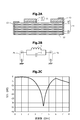
- 2A is a schematic cross-sectional view of a resonant circuit element actually manufactured
- FIG. 2B is an equivalent circuit diagram of a filter using the resonant circuit element of FIG. 2A
- FIG. 2C is a diagram of the filter shown in FIG. 2B. It is a graph which shows the measurement result of S parameter S21.
- FIG. 3A is a plan view of the resonant circuit element according to the second embodiment
- FIG. 3B is an equivalent circuit diagram of the resonant circuit element according to the second embodiment.
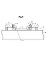
- FIG. 4 is a cross-sectional view of a circuit module according to the third embodiment.
- the resonant circuit element according to the first embodiment includes a flexible film 10, a first conductive pattern 11, an adhesive layer 12, and a pair of first external electrodes 13.
- the flexible film 10 is made of a dielectric material, for example, a resin such as polyimide.
- a first conductive pattern 11 is provided on one surface of the flexible film 10 (hereinafter referred to as the first surface 10A).
- a conductive material such as copper (Cu) is used.
- the first conductive pattern 11 has a meander-like planar shape.
- the first conductive pattern 11 can be formed by attaching a copper foil shaped into a desired shape to the flexible film 10 with an adhesive.
- the adhesive layer 12 is provided on the second surface 10B of the flexible film 10 opposite to the first surface 10A.
- a thermosetting or photocurable adhesive can be used for the adhesive layer 12.
- the flexible film 10 is formed of a material that transmits light in the wavelength region for curing. In a state where the resonant circuit element is not mounted, the adhesive layer 12 maintains adhesiveness.
- a laminate composed of the flexible film 10 and the adhesive layer 12 is referred to as a composite member 15.
- the composite member 15 has a dielectric constant lower than that of a general ceramic.
- a pair of first external electrodes 13 are formed on the end surface of the composite member 15.
- the planar shape of the composite member 15 is a rectangle, and the pair of first external electrodes 13 includes portions formed on end surfaces of the composite member 15 facing in opposite directions.
- a part of the first external electrode 13 covers a region in the vicinity of the edge of the first surface 10A.
- the first external electrode 13 may cover the vicinity of the edge of the second surface 10B.
- the first external electrode 13 can be formed using, for example, a printing technique.
- the pair of first external electrodes 13 are electrically connected to both ends of the first conductive pattern 11, respectively.
- the first conductive pattern 11 functions as an inductor L (FIG. 1C) connected between the pair of first external electrodes 13. Note that the planar shape of the first conductive pattern 11 does not have to be a meander shape, and may be other shapes depending on a desired inductance.
- the composite member 15 and the pair of first external electrodes 13 function as a capacitor C (FIG. 1C).
- FIG. 2A is a schematic cross-sectional view of the actually produced resonant circuit element.
- a flexible film 10 was formed by stacking five layers of polyimide tape coated with a heat-resistant silicone adhesive 21 on one side of the polyimide film 20.
- the planar shape of the flexible film 10 is a rectangle with long sides and short sides of about 2 cm and about 1 cm, respectively.
- the adhesive 21 of the lowermost polyimide tape corresponds to the adhesive layer 12 (FIGS. 1B and 1C).
- the thickness of the polyimide film 20 is 0.05 mm, and the relative dielectric constant is 3.3 at 1 MHz.
- the heat-resistant silicone-based adhesive 21 has a thickness of 0.02 mm and a relative dielectric constant of 3.3 at 1 MHz.
- the 1st conductive pattern 11 was formed by affixing the copper foil 22 with which the conductive adhesive 23 was apply
- the thickness of the copper foil 22 is 0.07 mm, and the thickness of the conductive adhesive 23 is 0.02 mm.
- the relative dielectric constant of the conductive adhesive 23 is 3.0 at 1 MHz.
- the first external electrode 13 was formed using a printing technique.
- FIG. 2B is an equivalent circuit diagram of a filter using a resonant circuit element. As shown in FIG. 2A, one terminal of the first port P1 and one terminal of the second port P2 are dropped to the ground, and between the other terminal of the first port P1 and the other terminal of the second port P2.
- the resonant circuit element that is, the parallel resonant circuit of the inductor L and the capacitor C is connected.
- FIG. 2C is a graph showing the measurement result of the S parameter S21 of the filter shown in FIG. 2B.
- the horizontal axis represents frequency in the unit “GHz”, and the vertical axis represents S21 in the unit “dB”.
- Resonance occurs at about 4.2 GHz, and S21 shows a minimum value.
- the resonant circuit element shown in FIG. 2A operates as an LC resonant circuit.
- the flexible film 10 is used for the resonant circuit element according to the first embodiment, it can be easily deformed. Therefore, even if the place to be mounted is not flat, the resonant circuit element can be deformed and mounted according to the shape of the place to be mounted. Further, the resonant circuit element can be attached to the mounting substrate with the surface where the adhesive layer 12 (FIG. 1B) is exposed facing the mounting substrate. By curing the adhesive layer 12 by heating or light irradiation after the attachment, the resonant circuit element can be easily fixed to the mounting substrate.
- the first external electrode 13 (FIG. 1B) can be electrically connected to the conductor portion to be connected, for example, with solder or the like.
- the first conductive pattern 11 (FIG. 1B) that operates as an inductor is formed of a single layer without being stacked, the first conductive pattern 11 can be thickened. By increasing the thickness of the first conductive pattern 11, the electric resistance of the first conductive pattern 11 can be reduced. For this reason, it is possible to cope with a large current. Furthermore, since the first conductive pattern 11 is not laminated, the thickness of the first conductive pattern 11 can be arbitrarily adjusted without affecting other structures. The inductance can be adjusted by adjusting the thickness of the first conductive pattern 11.
- FIG. 3A is a plan view of the resonant circuit element according to the second embodiment.
- the conductor portion is hatched.
- a second conductive pattern 17 is provided on the upper surface of the composite member 15.
- One first conductive pattern 11 and the other second conductive pattern 17 run in parallel in part, and both are electromagnetically coupled.
- a pair of second external electrodes 18 is formed on the end surface of the composite member 15.
- the pair of second external electrodes 18 are connected to both ends of the second conductive pattern 17, respectively.
- FIG. 3B is an equivalent circuit diagram of the resonant circuit element according to the second embodiment.
- a parallel resonant circuit of an inductor and a capacitor is connected between the pair of first external electrodes 13 as in the first embodiment, and the inductor and the capacitor are connected between the other pair of second external electrodes 18.
- a parallel resonant circuit is connected.
- the two inductors are coupled to each other and operate as a common mode choke coil.
- the leakage of common mode noise can be suppressed by inserting the resonant circuit element according to the second embodiment into the differential transmission path. Further, as shown in FIG. 2B, the LC parallel resonant circuit functions as a band elimination filter for the differential mode signal.
- FIG. 4 is a cross-sectional view of a circuit module according to the third embodiment.
- the printed circuit board 35 includes a printed wiring board 30 and circuit elements 31 and 32 mounted thereon.
- the printed circuit board 35 is provided with a plurality of conductive portions such as a plurality of lands for mounting circuit elements and terminals 33 and 34 of the mounted circuit elements 31 and 32. Since the upper surfaces of the circuit elements 31 and 32 are disposed higher than the upper surface of the printed wiring board 30, a step is provided on the upper surface of the printed circuit board 35.
- the resonant circuit element 40 is mounted on the printed circuit board 35.
- the resonance circuit element 40 the resonance circuit element (FIG. 1B) according to the first embodiment is used.
- One first external electrode 13 of the resonant circuit element 40 is placed on the terminal 33 of the circuit element 31 and is electrically connected by solder 41.
- the other first external electrode 13 of the resonant circuit element 40 is placed on the terminal 34 of the circuit element 32 and is electrically connected by solder 41.
- the resonant circuit element 40 is connected between the terminal 33 of the circuit element 31 and the terminal 34 of the circuit element 32.
- a step is formed due to the height of the circuit elements 31 and 32.
- the composite member 15 of the resonant circuit element 40 is deformed reflecting the step on the upper surface of the printed circuit board 35.
- the adhesive layer 12 of the resonant circuit element 40 is bonded to the upper surface of the printed circuit board 35 and cured.
- the resonant circuit element 40 can be fixed to the printed circuit board 35 by curing the adhesive layer 12.
- the excellent effect of the resonant circuit element 40 according to the third embodiment will be described.
- a hard material such as ceramic
- the hard resonant circuit element is bridged between the circuit elements 31 and 32 and supported in a hollow state.
- the resonant circuit element 40 is deformed according to the step on the upper surface of the printed circuit board 35, and is adhered and fixed to the upper surface of the printed circuit board 35 between the circuit elements 31 and 32. For this reason, the resonance circuit element 40 can be fixed firmly and durability can be improved.
- the resonant circuit element 40 can be mounted over the circuit element mounted on the printed wiring board 50.
Landscapes
- Engineering & Computer Science (AREA)
- Power Engineering (AREA)
- Microelectronics & Electronic Packaging (AREA)
- Physics & Mathematics (AREA)
- Electromagnetism (AREA)
- Manufacturing & Machinery (AREA)
- Multimedia (AREA)
- Coils Or Transformers For Communication (AREA)
- Fixed Capacitors And Capacitor Manufacturing Machines (AREA)
- Structure Of Printed Boards (AREA)
- Filters And Equalizers (AREA)
- Parts Printed On Printed Circuit Boards (AREA)
Abstract
誘電体材料からなるフレキシブルフィルムの一方の面である第1の面に導電材料からなる第1の導電パターンが形成されている。フレキシブルフィルムの第1の面とは反対側の第2の面に接着剤層が設けられている。一対の第1の外部電極が、フレキシブルフィルムと接着剤層とからなる複合部材に面内方向の電界を生じさせるとともに、第1の導電パターンに電流を流す。
Description
本発明は、共振回路素子及び回路モジュールに関する。
電子機器のノイズ、特に高周波におけるノイズの対策として、電磁妨害(EMI)フィルタが使用されている。下記の特許文献1に、インダクタとコンデンサとを並列に備えるEMIフィルタが開示されている。このEMIフィルタのコンデンサは、複数の接地導体層と他方の複数の導体層とが、セラミック層を介して交互に積層された多層構造を有する。インダクタは、コンデンサの複数の非接地導体層と同一の層に設けられた導体パターンで構成される。
特許文献1に開示されたEMIフィルタはセラミック層を含む多層構造を有しているため、機械的な柔軟性に欠ける。このため、実装すべき箇所の幾何学的形状に制約を受ける。
本発明の目的は、種々の形状を有する箇所に実装することが可能な共振回路素子を提供することである。本発明の他の目的は、この共振回路素子が実装された回路モジュールを提供することである。
本発明の第1の観点による共振回路素子は、
誘電体材料からなるフレキシブルフィルムと、
前記フレキシブルフィルムの一方の面である第1の面に形成された導電材料からなる第1の導電パターンと、
前記フレキシブルフィルムの前記第1の面とは反対側の第2の面に設けられた接着剤層と、
前記フレキシブルフィルムと前記接着剤層とからなる複合部材に面内方向の電界を生じさせるとともに、前記第1の導電パターンに電流を流す一対の第1の外部電極と
を有する。
誘電体材料からなるフレキシブルフィルムと、
前記フレキシブルフィルムの一方の面である第1の面に形成された導電材料からなる第1の導電パターンと、
前記フレキシブルフィルムの前記第1の面とは反対側の第2の面に設けられた接着剤層と、
前記フレキシブルフィルムと前記接着剤層とからなる複合部材に面内方向の電界を生じさせるとともに、前記第1の導電パターンに電流を流す一対の第1の外部電極と
を有する。
第1の導電パターンがインダクタとして機能し、一対の外部電極と複合部材とがコンデンサとして機能する。このインダクタとコンデンサとにより、LC共振回路が構成される。フレキシブルフィルムを変形させることにより、種々の幾何学的形状を有する実装箇所に実装することができる。接着剤層により共振回路素子を実装箇所に貼り付けることができる。
本発明の第2の観点による共振回路素子は、第1の観点による共振回路素子の構成に加えて、
一対の前記第1の外部電極の各々が、前記複合部材の端面に形成された部分を含むという特徴を有する。
一対の前記第1の外部電極の各々が、前記複合部材の端面に形成された部分を含むという特徴を有する。
一対の外部電極を複合部材の端面に形成することにより、複合部材の面内方向に効率的に電界を発生させることができる。
本発明の第3の観点による共振回路素子は、第1または第2の観点による共振回路素子の構成に加えて、
前記第1の面に形成された導電材料からなる第2の導電パターンと、
前記第2の導電パターンに電流を流すとともに、前記複合部材に面内方向の電界を生じさせる一対の第2の外部電極と
を有し、
前記第1の導電パターンと前記第2の導電パターンとがチョークコイルを構成している。
前記第1の面に形成された導電材料からなる第2の導電パターンと、
前記第2の導電パターンに電流を流すとともに、前記複合部材に面内方向の電界を生じさせる一対の第2の外部電極と
を有し、
前記第1の導電パターンと前記第2の導電パターンとがチョークコイルを構成している。
実装箇所の幾何学的形状に応じて柔軟に変形するチョークコイルを実現することができる。さらに、一対の第1の外部電極の間を接続するLC共振回路が帯域除去フィルタとして機能する。同様に、一対の第2の外部電極の間を接続するLC共振回路が帯域除去フィルタとして機能する。
本発明の第4の観点による共振回路素子は、第1から第3までの観点による共振回路素子の構成に加えて、
前記接着剤層が、熱硬化型または光硬化型の接着剤で形成されているという特徴を有する。
前記接着剤層が、熱硬化型または光硬化型の接着剤で形成されているという特徴を有する。
共振回路素子の接着剤層を実装箇所に接着した後、加熱または光照射を行うことにより、容易に接着剤層を硬化させることができる。
本発明の第5の観点による回路モジュールは、
複数の導電部分が設けられたプリント回路板と、
前記プリント回路板に実装され、2つの前記導電部分の間を接続する共振回路素子と
を有し、
前記共振回路素子は、
誘電体材料からなるフレキシブルフィルムと、
前記フレキシブルフィルムの一方の面である第1の面に形成された導電材料からなる第1の導電パターンと、
前記フレキシブルフィルムの前記第1の面とは反対側の第2の面に設けられた接着剤層と、
前記フレキシブルフィルムと前記接着剤層とからなる複合部材に面内方向の電界を生じさせるとともに、前記第1の導電パターンに電流を流す一対の外部電極と
を有し、
一対の前記外部電極が、それぞれ2つの前記導電部分に電気的に接続されており、前記接着剤層によって前記プリント回路板に接着されている。
複数の導電部分が設けられたプリント回路板と、
前記プリント回路板に実装され、2つの前記導電部分の間を接続する共振回路素子と
を有し、
前記共振回路素子は、
誘電体材料からなるフレキシブルフィルムと、
前記フレキシブルフィルムの一方の面である第1の面に形成された導電材料からなる第1の導電パターンと、
前記フレキシブルフィルムの前記第1の面とは反対側の第2の面に設けられた接着剤層と、
前記フレキシブルフィルムと前記接着剤層とからなる複合部材に面内方向の電界を生じさせるとともに、前記第1の導電パターンに電流を流す一対の外部電極と
を有し、
一対の前記外部電極が、それぞれ2つの前記導電部分に電気的に接続されており、前記接着剤層によって前記プリント回路板に接着されている。
共振回路素子をプリント回路板に接着することにより、容易にプリント回路板に固定することができる。
本発明の第6の観点による回路モジュールは、第5の観点による回路モジュールの構成に加えて、
前記プリント回路板の、前記共振回路素子が実装されている箇所に段差が設けられており、前記共振回路素子は前記プリント回路板の段差を反映して変形しているという特徴を有する。
前記プリント回路板の、前記共振回路素子が実装されている箇所に段差が設けられており、前記共振回路素子は前記プリント回路板の段差を反映して変形しているという特徴を有する。
共振回路素子を変形させることにより、種々の段差が設けられたプリント回路板に容易に実装することが可能になる。
第1の導電パターンがインダクタとして機能し、一対の外部電極と複合部材とがコンデンサとして機能する。このインダクタとコンデンサとにより、LC共振回路が構成される。フレキシブルフィルムを変形させることにより、種々の幾何学的形状を有する実装箇所に実装することができる。接着剤層により共振回路素子を実装箇所に貼り付けることができる。
[第1実施例]
図1Aから図2Cまでの図面を参照して、第1実施例による共振回路素子について説明する。
図1Aから図2Cまでの図面を参照して、第1実施例による共振回路素子について説明する。
図1A、図1B、及び図1Cは、それぞれ第1実施例による共振回路素子の分解斜視図、斜視図、及び断面図である。第1実施例による共振回路素子は、フレキシブルフィルム10、第1の導電パターン11、接着剤層12、及び一対の第1の外部電極13を含む。
フレキシブルフィルム10には、誘電体材料、例えばポリイミド等の樹脂が用いられる。フレキシブルフィルム10の一方の表面(以下、第1の面10Aという。)に第1の導電パターン11が設けられている。第1の導電パターン11には、導電材料、例えば銅(Cu)等が用いられる。第1の導電パターン11は、メアンダ状の平面形状を有する。第1の導電パターン11は、所望の形状に整形された銅箔を接着剤でフレキシブルフィルム10に貼り付けることにより形成することができる。
フレキシブルフィルム10の、第1の面10Aとは反対側の第2の面10Bに、接着剤層12が設けられている。接着剤層12には、例えば熱硬化型または光硬化型の接着剤を用いることができる。接着剤層12に光硬化型の接着剤を用いる場合には、フレキシブルフィルム10は硬化用の波長域の光を透過させる材料で形成される。共振回路素子が未実装の状態では、接着剤層12が粘着性を維持している。フレキシブルフィルム10及び接着剤層12からなる積層体を複合部材15ということとする。複合部材15は、一般的なセラミックより低い誘電率を有する。
複合部材15の端面に、一対の第1の外部電極13が形成されている。例えば、複合部材15の平面形状は長方形であり、一対の第1の外部電極13は、複合部材15の相互に反対方向を向く端面に形成された部分を含む。第1の外部電極13の一部分は、第1の面10Aの縁の近傍の領域を覆う。なお、第1の外部電極13が第2の面10Bの縁の近傍を覆うようにしてもよい。第1の外部電極13は、例えば印刷技術を用いて形成することができる。一対の第1の外部電極13は、それぞれ第1の導電パターン11の両端に電気的に接続されている。一対の第1の外部電極13に電位差を生じさせると、複合部材15に主として面内方向の電界が生じるとともに、第1の導電パターン11に電流が流れる。第1の導電パターン11は、一対の第1の外部電極13の間に接続されたインダクタL(図1C)として機能する。なお、第1の導電パターン11の平面形状はメアンダ状である必要は無く、所望のインダクタンスに応じてその他の形状としてよい。複合部材15及び一対の第1の外部電極13はコンデンサC(図1C)として機能する。
次に、第1実施例による共振回路素子を実際に作製して電気的特性を測定した結果について説明する。
図2Aは、実際に作製した共振回路素子の概略断面図である。ポリイミドフィルム20の片面に耐熱シリコーン系の接着剤21が塗布されたポリイミドテープを5層重ねてフレキシブルフィルム10を構成した。フレキシブルフィルム10の平面形状は、長辺及び短辺の長さがそれぞれ約2cm及び約1cmの長方形である。最下層のポリイミドテープの接着剤21が、接着剤層12(図1B、図1C)に相当する。ポリイミドフィルム20の厚さは0.05mmであり、比誘電率は1MHzにおいて3.3である。耐熱シリコーン系の接着剤21の厚さは0.02mmであり、比誘電率は1MHzにいて3.3である。
片面に導電性接着剤23が塗布された銅箔22をフレキシブルフィルム10に貼り付けることにより、第1の導電パターン11を形成した。銅箔22の厚さは0.07mmであり、導電性接着剤23の厚さは0.02mmである。導電性接着剤23の比誘電率は、1MHzにおいて3.0である。第1の外部電極13は印刷技術を用いて形成した。
図2Bは、共振回路素子を用いたフィルタの等価回路図である。第1ポートP1の一方の端子と第2ポートP2の一方の端子とがグランドに落とされ、第1ポートP1の他方の端子と第2ポートP2の他方の端子との間に、図2Aに示した共振回路素子、すなわちインダクタLとコンデンサCとの並列共振回路が接続される。
図2Cは、図2Bに示したフィルタのSパラメータS21の測定結果を示すグラフである。横軸は周波数を単位「GHz」で表し、縦軸はS21を単位「dB」で表す。約4.2GHzで共振が生じ、S21が極小値を示している。このように、図2Aに示した共振回路素子がLC共振回路として動作することが確認された。
次に、第1実施例による共振回路素子が有する優れた効果について説明する。
第1実施例による共振回路素子にはフレキシブルフィルム10が用いられているため、容易に変形させることが可能である。従って、実装すべき箇所が平坦ではない場合であっても、実装すべき箇所の形状に応じて共振回路素子を変形させて実装することが可能である。また、接着剤層12(図1B)が露出している面を実装基板に対向させて共振回路素子を実装基板に貼り付けることができる。貼り付けた後に接着剤層12を加熱または光照射等によって硬化させることにより、共振回路素子を実装基板に容易に固定することができる。第1の外部電極13(図1B)は、例えばはんだ等により接続先の導体部分に電気的に接続することができる。
第1実施例による共振回路素子にはフレキシブルフィルム10が用いられているため、容易に変形させることが可能である。従って、実装すべき箇所が平坦ではない場合であっても、実装すべき箇所の形状に応じて共振回路素子を変形させて実装することが可能である。また、接着剤層12(図1B)が露出している面を実装基板に対向させて共振回路素子を実装基板に貼り付けることができる。貼り付けた後に接着剤層12を加熱または光照射等によって硬化させることにより、共振回路素子を実装基板に容易に固定することができる。第1の外部電極13(図1B)は、例えばはんだ等により接続先の導体部分に電気的に接続することができる。
インダクタとして動作する第1の導電パターン11(図1B)が積層されることなく単層で構成されているため、第1の導電パターン11を厚くすることが可能である。第1の導電パターン11を厚くすることにより、第1の導電パターン11の電気抵抗を低減させることができる。このため、大電流に対応することが可能である。さらに、第1の導電パターン11が積層されないため、他の構造に影響を与えることなく第1の導電パターン11の厚さを任意に調整することができる。第1の導電パターン11の厚さを調整することにより、インダクタンスを調整することが可能である。
[第2実施例]
次に、図3A及び図3Bを参照して第2実施例による共振回路素子について説明する。以下、第1実施例による共振回路素子と共通の構成については説明を省略する。
次に、図3A及び図3Bを参照して第2実施例による共振回路素子について説明する。以下、第1実施例による共振回路素子と共通の構成については説明を省略する。
図3Aは、第2実施例による共振回路素子の平面図である。図3Aにおいて導体部分にハッチングが付されている。複合部材15の上面に、第1の導電パターン11の他に第2の導電パターン17が設けられている。一方の第1の導電パターン11と他方の第2の導電パターン17とは一部分において並走しており、両者は電磁的に結合している。
複合部材15の端面に、一対の第1の外部電極13の他に一対の第2の外部電極18が形成されている。一対の第2の外部電極18は、それぞれ第2の導電パターン17の両端に接続されている。
図3Bは、第2実施例による共振回路素子の等価回路図である。一対の第1の外部電極13の間に、第1実施例と同様にインダクタとコンデンサとの並列共振回路が接続され、他の一対の第2の外部電極18の間にもインダクタとコンデンサとの並列共振回路が接続される。2つのインダクタが相互に結合し、コモンモードチョークコイルとして動作する。
第2実施例による共振回路素子を差動伝送路に挿入することにより、コモンモードノイズの漏洩を抑制することができる。さらに、図2Bに示したように、LC並列共振回路がディファレンシャルモード信号に対して帯域除去フィルタとして機能する。
[第3実施例]
次に、図4を参照して第3実施例による回路モジュールについて説明する。
図4は、第3実施例による回路モジュールの断面図である。プリント回路板35が、プリント配線板30、及びそれに実装された回路素子31、32を含む。プリント回路板35には、回路素子を実装するための複数のランド、実装された回路素子31、32の端子33、34等の複数の導電部分が設けられている。回路素子31、32の上面はプリント配線板30の上面より高い位置に配置されるため、プリント回路板35の上面には段差が設けられることになる。
次に、図4を参照して第3実施例による回路モジュールについて説明する。
図4は、第3実施例による回路モジュールの断面図である。プリント回路板35が、プリント配線板30、及びそれに実装された回路素子31、32を含む。プリント回路板35には、回路素子を実装するための複数のランド、実装された回路素子31、32の端子33、34等の複数の導電部分が設けられている。回路素子31、32の上面はプリント配線板30の上面より高い位置に配置されるため、プリント回路板35の上面には段差が設けられることになる。
プリント回路板35に共振回路素子40が実装されている。共振回路素子40として第1実施例による共振回路素子(図1B)が用いられる。共振回路素子40の一方の第1の外部電極13が回路素子31の端子33の上に載せられて、はんだ41により電気的に接続されている。共振回路素子40の他方の第1の外部電極13が回路素子32の端子34の上に載せられて、はんだ41により電気的に接続されている。共振回路素子40は、回路素子31の端子33と回路素子32の端子34との間に接続される。
共振回路素子40が実装された箇所には、回路素子31、32の高さに起因して段差が形成されている。共振回路素子40の複合部材15は、プリント回路板35の上面の段差を反映して変形している。共振回路素子40の接着剤層12がプリント回路板35の上面に接着されて硬化されている。接着剤層12を硬化させることにより、共振回路素子40をプリント回路板35に固定することができる。
次に、第3実施例による共振回路素子40が有する優れた効果について説明する。共振回路素子にセラミック等の硬い材料が用いられる場合には、プリント回路板35の上面の段差に応じて変形させることができない。図4に示した例では、硬い共振回路素子が回路素子31と32との間に架け渡されて中空に支持されることになる。
第3実施例においては、共振回路素子40がプリント回路板35の上面の段差に応じて変形し、回路素子31と32との間のプリント回路板35の上面に接着されて固定される。このため、共振回路素子40を強固に固定し、耐久性を高めることができる。
例えば、回路モジュールの設計完了後に、ノイズ対策として共振回路素子40を実装することが可能である。共振回路素子40は、プリント配線板50に実装された回路素子の上に重ねて実装することが可能である。
上述の各実施例は例示であり、異なる実施例で示した構成の部分的な置換または組み合わせが可能であることは言うまでもない。複数の実施例の同様の構成による同様の作用効果については実施例ごとには逐次言及しない。さらに、本発明は上述の実施例に制限されるものではない。例えば、種々の変更、改良、組み合わせ等が可能なことは当業者に自明であろう。
10 フレキシブルフィルム
10A 第1の面
10B 第2の面
11 第1の導電パターン
12 接着剤層
13 第1の外部電極
15 複合部材
17 第2の導電パターン
18 第2の外部電極
20 ポリイミドフィルム
21 接着剤
22 銅箔
23 導電性接着剤
30 プリント配線板
31、32 回路素子
33、34 端子
35 プリント回路板
40 共振回路素子
41 はんだ
10A 第1の面
10B 第2の面
11 第1の導電パターン
12 接着剤層
13 第1の外部電極
15 複合部材
17 第2の導電パターン
18 第2の外部電極
20 ポリイミドフィルム
21 接着剤
22 銅箔
23 導電性接着剤
30 プリント配線板
31、32 回路素子
33、34 端子
35 プリント回路板
40 共振回路素子
41 はんだ
Claims (6)
- 誘電体材料からなるフレキシブルフィルムと、
前記フレキシブルフィルムの一方の面である第1の面に形成された導電材料からなる第1の導電パターンと、
前記フレキシブルフィルムの前記第1の面とは反対側の第2の面に設けられた接着剤層と、
前記フレキシブルフィルムと前記接着剤層とからなる複合部材に面内方向の電界を生じさせるとともに、前記第1の導電パターンに電流を流す一対の第1の外部電極と
を有する共振回路素子。 - 一対の前記第1の外部電極の各々は、前記複合部材の端面に形成された部分を含む請求項1に記載の共振回路素子。
- さらに、
前記第1の面に形成された導電材料からなる第2の導電パターンと、
前記第2の導電パターンに電流を流すとともに、前記複合部材に面内方向の電界を生じさせる一対の第2の外部電極と
を有し、
前記第1の導電パターンと前記第2の導電パターンとがチョークコイルを構成する請求項1または2に記載の共振回路素子。 - 前記接着剤層は、熱硬化型または光硬化型の接着剤で形成されている請求項1乃至3のいずれか1項に記載の共振回路素子。
- 複数の導電部分が設けられたプリント回路板と、
前記プリント回路板に実装され、2つの前記導電部分の間を接続する共振回路素子と
を有し、
前記共振回路素子は、
誘電体材料からなるフレキシブルフィルムと、
前記フレキシブルフィルムの一方の面である第1の面に形成された導電材料からなる第1の導電パターンと、
前記フレキシブルフィルムの前記第1の面とは反対側の第2の面に設けられた接着剤層と、
前記フレキシブルフィルムと前記接着剤層とからなる複合部材に面内方向の電界を生じさせるとともに、前記第1の導電パターンに電流を流す一対の外部電極と
を有し、
一対の前記外部電極が、それぞれ2つの前記導電部分に電気的に接続されており、前記接着剤層によって前記プリント回路板に接着されている回路モジュール。 - 前記プリント回路板の、前記共振回路素子が実装されている箇所に段差が設けられており、前記共振回路素子は前記プリント回路板の段差を反映して変形している請求項5に記載の回路モジュール。
Priority Applications (3)
| Application Number | Priority Date | Filing Date | Title |
|---|---|---|---|
| CN201880017340.1A CN110402538B (zh) | 2017-05-08 | 2018-03-07 | 谐振电路元件以及电路模块 |
| JP2019516904A JP6658966B2 (ja) | 2017-05-08 | 2018-03-07 | 共振回路素子及び回路モジュール |
| US16/572,269 US11239813B2 (en) | 2017-05-08 | 2019-09-16 | Resonant circuit element and circuit module |
Applications Claiming Priority (2)
| Application Number | Priority Date | Filing Date | Title |
|---|---|---|---|
| JP2017092221 | 2017-05-08 | ||
| JP2017-092221 | 2017-05-08 |
Related Child Applications (1)
| Application Number | Title | Priority Date | Filing Date |
|---|---|---|---|
| US16/572,269 Continuation US11239813B2 (en) | 2017-05-08 | 2019-09-16 | Resonant circuit element and circuit module |
Publications (1)
| Publication Number | Publication Date |
|---|---|
| WO2018207447A1 true WO2018207447A1 (ja) | 2018-11-15 |
Family
ID=64105109
Family Applications (1)
| Application Number | Title | Priority Date | Filing Date |
|---|---|---|---|
| PCT/JP2018/008765 Ceased WO2018207447A1 (ja) | 2017-05-08 | 2018-03-07 | 共振回路素子及び回路モジュール |
Country Status (4)
| Country | Link |
|---|---|
| US (1) | US11239813B2 (ja) |
| JP (1) | JP6658966B2 (ja) |
| CN (1) | CN110402538B (ja) |
| WO (1) | WO2018207447A1 (ja) |
Families Citing this family (1)
| Publication number | Priority date | Publication date | Assignee | Title |
|---|---|---|---|---|
| US12300420B2 (en) * | 2021-02-25 | 2025-05-13 | Astrodyne TDI | Filter device having tunable capacitance, method of manufacture and use thereof |
Citations (4)
| Publication number | Priority date | Publication date | Assignee | Title |
|---|---|---|---|---|
| JPS5853807A (ja) * | 1981-09-26 | 1983-03-30 | Matsushita Electric Ind Co Ltd | 巻回型複合チツプ部品 |
| JPS58137206A (ja) * | 1982-02-09 | 1983-08-15 | Sony Corp | インダクタンス素子 |
| JP2008135430A (ja) * | 2006-11-27 | 2008-06-12 | Matsushita Electric Ind Co Ltd | 高周波モジュール |
| WO2011013662A1 (ja) * | 2009-07-28 | 2011-02-03 | ソニーケミカル&インフォメーションデバイス株式会社 | アンテナ装置、及び、通信装置 |
Family Cites Families (7)
| Publication number | Priority date | Publication date | Assignee | Title |
|---|---|---|---|---|
| JP2003249832A (ja) | 2002-02-22 | 2003-09-05 | Murata Mfg Co Ltd | Emiフィルタ |
| CN204991353U (zh) * | 2013-06-14 | 2016-01-20 | 株式会社村田制作所 | 柔性电感器的安装结构及电子设备 |
| US20140369081A1 (en) * | 2013-06-18 | 2014-12-18 | Microsemi Corporation | Power converter |
| CN103560763B (zh) * | 2013-11-08 | 2017-08-01 | 诺思(天津)微系统有限公司 | 片上集成型体波谐振器及其制造方法 |
| CN205490448U (zh) * | 2015-03-19 | 2016-08-17 | 中科鼎源(北京)科技有限公司 | 一种新型声表面波器件 |
| KR20170011067A (ko) * | 2015-07-21 | 2017-02-02 | 주식회사 엠플러스 | 압전진동모듈 |
| JP6540808B2 (ja) * | 2015-07-24 | 2019-07-10 | 株式会社村田製作所 | フレキシブルインダクタ |
-
2018
- 2018-03-07 CN CN201880017340.1A patent/CN110402538B/zh active Active
- 2018-03-07 WO PCT/JP2018/008765 patent/WO2018207447A1/ja not_active Ceased
- 2018-03-07 JP JP2019516904A patent/JP6658966B2/ja active Active
-
2019
- 2019-09-16 US US16/572,269 patent/US11239813B2/en active Active
Patent Citations (4)
| Publication number | Priority date | Publication date | Assignee | Title |
|---|---|---|---|---|
| JPS5853807A (ja) * | 1981-09-26 | 1983-03-30 | Matsushita Electric Ind Co Ltd | 巻回型複合チツプ部品 |
| JPS58137206A (ja) * | 1982-02-09 | 1983-08-15 | Sony Corp | インダクタンス素子 |
| JP2008135430A (ja) * | 2006-11-27 | 2008-06-12 | Matsushita Electric Ind Co Ltd | 高周波モジュール |
| WO2011013662A1 (ja) * | 2009-07-28 | 2011-02-03 | ソニーケミカル&インフォメーションデバイス株式会社 | アンテナ装置、及び、通信装置 |
Also Published As
| Publication number | Publication date |
|---|---|
| US11239813B2 (en) | 2022-02-01 |
| CN110402538A (zh) | 2019-11-01 |
| JP6658966B2 (ja) | 2020-03-04 |
| US20200014361A1 (en) | 2020-01-09 |
| CN110402538B (zh) | 2021-01-15 |
| JPWO2018207447A1 (ja) | 2019-11-07 |
Similar Documents
| Publication | Publication Date | Title |
|---|---|---|
| US11309114B2 (en) | Stacked body and method of producing stacked body | |
| JP6156610B2 (ja) | 電子機器、およびアンテナ素子 | |
| JP4842346B2 (ja) | 電子部品モジュールおよびその製造方法 | |
| JP6132054B2 (ja) | アンテナ装置 | |
| CN208016128U (zh) | 多层基板及电子设备 | |
| CN211606926U (zh) | 内插器以及电子设备 | |
| CN104575938A (zh) | 线圈组件及其制造方法、基板及具有基板的电压调整模块 | |
| US10861757B2 (en) | Electronic component with shield plate and shield plate of electronic component | |
| JP5765507B1 (ja) | インダクタ素子及び電子機器 | |
| US20130250528A1 (en) | Circuit module | |
| KR101905879B1 (ko) | 인쇄회로기판 및 그의 제조 방법 | |
| JP6406474B2 (ja) | 表面実装型シールド部材及び回路モジュール | |
| JP6558514B2 (ja) | 電子機器 | |
| JP6658966B2 (ja) | 共振回路素子及び回路モジュール | |
| WO2020049989A1 (ja) | モジュールおよびモジュールの製造方法 | |
| JP6563129B2 (ja) | フレキシブルプリント基板 | |
| JP5178351B2 (ja) | 電子部品の実装構造 | |
| CN211828497U (zh) | 树脂多层基板以及电子设备 | |
| JP2004266180A (ja) | 配線基板 | |
| WO2020196131A1 (ja) | 電子部品モジュール | |
| WO2018051858A1 (ja) | 電子部品 | |
| JP2005011927A (ja) | 複合回路基板 | |
| WO2024080331A1 (ja) | Rfidモジュール | |
| JP2024153955A (ja) | 回路基板及び電子部品 | |
| JP2014130985A (ja) | 多層回路基板 |
Legal Events
| Date | Code | Title | Description |
|---|---|---|---|
| 121 | Ep: the epo has been informed by wipo that ep was designated in this application |
Ref document number: 18798018 Country of ref document: EP Kind code of ref document: A1 |
|
| ENP | Entry into the national phase |
Ref document number: 2019516904 Country of ref document: JP Kind code of ref document: A |
|
| NENP | Non-entry into the national phase |
Ref country code: DE |
|
| 122 | Ep: pct application non-entry in european phase |
Ref document number: 18798018 Country of ref document: EP Kind code of ref document: A1 |