WO2018190408A1 - 光学素子及び光学薄膜 - Google Patents
光学素子及び光学薄膜 Download PDFInfo
- Publication number
- WO2018190408A1 WO2018190408A1 PCT/JP2018/015466 JP2018015466W WO2018190408A1 WO 2018190408 A1 WO2018190408 A1 WO 2018190408A1 JP 2018015466 W JP2018015466 W JP 2018015466W WO 2018190408 A1 WO2018190408 A1 WO 2018190408A1
- Authority
- WO
- WIPO (PCT)
- Prior art keywords
- film
- hydrophilic
- optical
- porosity
- optical element
- Prior art date
- Legal status (The legal status is an assumption and is not a legal conclusion. Google has not performed a legal analysis and makes no representation as to the accuracy of the status listed.)
- Ceased
Links
Images





Classifications
-
- C—CHEMISTRY; METALLURGY
- C23—COATING METALLIC MATERIAL; COATING MATERIAL WITH METALLIC MATERIAL; CHEMICAL SURFACE TREATMENT; DIFFUSION TREATMENT OF METALLIC MATERIAL; COATING BY VACUUM EVAPORATION, BY SPUTTERING, BY ION IMPLANTATION OR BY CHEMICAL VAPOUR DEPOSITION, IN GENERAL; INHIBITING CORROSION OF METALLIC MATERIAL OR INCRUSTATION IN GENERAL
- C23C—COATING METALLIC MATERIAL; COATING MATERIAL WITH METALLIC MATERIAL; SURFACE TREATMENT OF METALLIC MATERIAL BY DIFFUSION INTO THE SURFACE, BY CHEMICAL CONVERSION OR SUBSTITUTION; COATING BY VACUUM EVAPORATION, BY SPUTTERING, BY ION IMPLANTATION OR BY CHEMICAL VAPOUR DEPOSITION, IN GENERAL
- C23C14/00—Coating by vacuum evaporation, by sputtering or by ion implantation of the coating forming material
- C23C14/06—Coating by vacuum evaporation, by sputtering or by ion implantation of the coating forming material characterised by the coating material
- C23C14/08—Oxides
-
- C—CHEMISTRY; METALLURGY
- C23—COATING METALLIC MATERIAL; COATING MATERIAL WITH METALLIC MATERIAL; CHEMICAL SURFACE TREATMENT; DIFFUSION TREATMENT OF METALLIC MATERIAL; COATING BY VACUUM EVAPORATION, BY SPUTTERING, BY ION IMPLANTATION OR BY CHEMICAL VAPOUR DEPOSITION, IN GENERAL; INHIBITING CORROSION OF METALLIC MATERIAL OR INCRUSTATION IN GENERAL
- C23C—COATING METALLIC MATERIAL; COATING MATERIAL WITH METALLIC MATERIAL; SURFACE TREATMENT OF METALLIC MATERIAL BY DIFFUSION INTO THE SURFACE, BY CHEMICAL CONVERSION OR SUBSTITUTION; COATING BY VACUUM EVAPORATION, BY SPUTTERING, BY ION IMPLANTATION OR BY CHEMICAL VAPOUR DEPOSITION, IN GENERAL
- C23C14/00—Coating by vacuum evaporation, by sputtering or by ion implantation of the coating forming material
- C23C14/06—Coating by vacuum evaporation, by sputtering or by ion implantation of the coating forming material characterised by the coating material
- C23C14/10—Glass or silica
-
- C—CHEMISTRY; METALLURGY
- C23—COATING METALLIC MATERIAL; COATING MATERIAL WITH METALLIC MATERIAL; CHEMICAL SURFACE TREATMENT; DIFFUSION TREATMENT OF METALLIC MATERIAL; COATING BY VACUUM EVAPORATION, BY SPUTTERING, BY ION IMPLANTATION OR BY CHEMICAL VAPOUR DEPOSITION, IN GENERAL; INHIBITING CORROSION OF METALLIC MATERIAL OR INCRUSTATION IN GENERAL
- C23C—COATING METALLIC MATERIAL; COATING MATERIAL WITH METALLIC MATERIAL; SURFACE TREATMENT OF METALLIC MATERIAL BY DIFFUSION INTO THE SURFACE, BY CHEMICAL CONVERSION OR SUBSTITUTION; COATING BY VACUUM EVAPORATION, BY SPUTTERING, BY ION IMPLANTATION OR BY CHEMICAL VAPOUR DEPOSITION, IN GENERAL
- C23C14/00—Coating by vacuum evaporation, by sputtering or by ion implantation of the coating forming material
- C23C14/22—Coating by vacuum evaporation, by sputtering or by ion implantation of the coating forming material characterised by the process of coating
- C23C14/24—Vacuum evaporation
- C23C14/28—Vacuum evaporation by wave energy or particle radiation
- C23C14/30—Vacuum evaporation by wave energy or particle radiation by electron bombardment
-
- G—PHYSICS
- G02—OPTICS
- G02B—OPTICAL ELEMENTS, SYSTEMS OR APPARATUS
- G02B1/00—Optical elements characterised by the material of which they are made; Optical coatings for optical elements
- G02B1/10—Optical coatings produced by application to, or surface treatment of, optical elements
- G02B1/11—Anti-reflection coatings
- G02B1/113—Anti-reflection coatings using inorganic layer materials only
- G02B1/115—Multilayers
Definitions
- the present invention generally relates to optical thin films.
- optical element is an optical lens (for example, a glass lens) mounted on a camera such as a still camera or a video camera. It is known that when an image is taken in a state where water droplets (for example, mist) are attached to the lens surface, the quality of the taken image is deteriorated.
- a camera such as a still camera or a video camera.
- an antireflection film is formed on a lens for a camera in order to increase the transmittance and improve the quality of a captured image. For this reason, forming the hydrophilic film disclosed in Patent Document 1 on a lens for a camera forms such a hydrophilic film on the antireflection film of the optical lens.
- This type of problem can also be caused by optical thin films on optical elements other than optical lenses.
- the optical thin film disclosed in Patent Document 1 is a multilayer film, the uppermost film is a hydrophilic film having irregularities on the surface, and the next film of the uppermost layer is a film that exhibits a photocatalytic reaction. . According to the inventor's consideration, the expected hydrophilicity cannot be obtained with such a multilayer film.
- An object of one embodiment of the present invention is to provide an optical thin film having both hydrophilicity and antireflection function.
- the optical thin film according to an embodiment of the present invention is a multilayer film.
- the uppermost film is a hydrophilic film that is a porous film.
- the next film after the uppermost layer is a base film which is a dense film.
- the porosity of the hydrophilic film is 2% or more and 20% or less, and the physical film thickness of the hydrophilic film is 0.5 nm or more and 20 nm or less.
- the porosity of the base film is less than 2%.
- an optical thin film having both hydrophilicity and antireflection function can be provided.
- the concept of the structure of the optical lens which concerns on embodiment of this invention is shown. It is a schematic diagram explaining the function of a hydrophilic film
- the structure of the multilayer film which concerns on embodiment of this invention is shown. 1 shows an optical thin film forming system according to an embodiment of the present invention. The relationship between the difference of the porosity of a base film and the difference of the time-sequential change of the contact angle of the water droplet adhering to a hydrophilic film
- the structure of the multilayer film which concerns on the comparative example of the experiment shown in FIG. 5 is shown.
- membrane and the contact angle of the water droplet after a fixed time after a water droplet is dripped is shown.
- 3 shows first and second spectral reflectance characteristics of the optical lens according to the embodiment.
- the structure of the multilayer film which concerns on the comparative example of the experiment shown in FIG. 8 is shown.
- the 1st modification of the structure of a multilayer film is shown.
- the 2nd modification of the structure of a multilayer film is shown.
- the 3rd modification of a structure of a multilayer film is shown.
- optical lenses according to some embodiments of the present invention will be described.
- the embodiments described below do not limit the invention according to the claims, and all the elements and combinations described in the embodiments are essential for the solution of the invention. Is not limited.
- FIG. 1 shows the concept of the configuration of an optical lens according to an embodiment of the present invention.
- the optical lens 100 includes an optical lens main body 101 and a multilayer film 102 that is an optical thin film formed on the surface of the optical lens main body 101.
- the multilayer film 102 is a plurality of overlapping (hierarchical) films.
- the multilayer film 102 has both hydrophilicity and antireflection function.
- the first layer (uppermost layer) is a hydrophilic film 111 that is a porous film.
- the film of the second layer (the layer next to the uppermost layer) is a base film 122 that is a dense film.
- the film other than the first and second layers is an antireflection film 121 composed of one or more films having an antireflection function.
- the base film 122 is located between the hydrophilic film 111 and the antireflection film 121. Optically, the refractive index and physical film thickness of each layer are determined so that the entire optical lens 100 provided with the multilayer film 102 has a desired spectral reflectance.
- FIG. 2 is a schematic diagram for explaining the functions of the hydrophilic film 111 and the base film 122.
- the layer on the optical lens body 101 side is referred to as a “lower layer”, and the layer on the surface side of the optical lens 100 (on the side opposite to the optical lens body 101 side). Is called the “upper layer”, and the vertical direction (the direction of film overlap) and the vertical direction are called the “horizontal direction”.
- the hydrophilic film 111 is a porous film as described above and can absorb moisture in the atmosphere by capillary action.
- the porosity of the hydrophilic film 111 is 2% or more and 20% or less.
- the physical film thickness of the hydrophilic film 111 is 0.5 nm (nanometer) or more and 20 nm or less.
- the base film 122 is a dense film having a porosity of less than 2%, and prevents (blocks) the progress of water from the hydrophilic film 111 to the lower layer. As a result, it is difficult for the moisture absorbed by the hydrophilic film 111 to enter the base film 122 from the hydrophilic film 111, so that the moisture is retained in the hydrophilic film 111. As a result, the hydrophilic film 111 Becomes the water retention layer.
- the water droplet 281 when water droplets 281 adhere to the surface of the hydrophilic film 111 as shown in FIG. Further, the water droplet 281 is absorbed by the hydrophilic film 111 due to capillary action, and as shown in (D), the water droplet 281 takes a relatively long time (for example, several tens of seconds to several minutes) to the hydrophilic film 111. Extends while absorbing moisture.
- the extension of water droplets in the hydrophilic film 111 means that the water droplets spread in the horizontal direction.
- the contact angle of the water droplets attached to the hydrophilic film 111 is the maximum contact angle (for example, static contact). Means the minimum contact angle.
- the amount of water droplets 281 adhering to the surface of the hydrophilic film 111 per unit time is larger (the amount of water retained than the amount of water that evaporates).
- the hydrophilic film 111 becomes the water retention layer W as shown in FIG. This is because the progress of water absorbed by the hydrophilic film 111 to the lower layer is blocked by the base film 122, and as a result, moisture is retained in the hydrophilic film 111.
- extension of the water droplets 281 attached to the hydrophilic film 111 serving as the water retention layer W is completed in a short time (for example, 5 seconds or less). This is because the pores in the porous membrane are already filled with water and the water droplets 281 expand so as to be integrated with the water.
- the physical film thickness of the hydrophilic film 111 is small, specifically, as described above, 0.5 nm (nanometer) or more and 20 nm or less. Thereby, even if it absorbs moisture, the change in reflectance characteristics is small.
- the physical film thickness of the hydrophilic film 111 may be smaller than the physical film thickness of the base film 122.
- the next film of the hydrophilic film 111 is the dense base film 122 having a porosity of less than 2%, and water intrusion into the base film 122 is blocked. The For this reason, there is little change in refractive index. As a result, there is little change in reflectance characteristics.
- each film in the multilayer film 102 is selected so that desired antireflection characteristics can be obtained as a whole including the hydrophilic film 111 and the base film 122.
- FIG. 3 shows a configuration of the multilayer film 102 according to the embodiment.
- the film having the layer number X (Xth layer) is referred to as “film X”.
- the minimum value of X is 1, and the film 1 is the lowermost film.
- the multilayer film 102 is composed of eight films.
- the antireflection film 121 is the films 1 to 6
- the base film 122 is the film 7
- the hydrophilic film 111 is the film 8.
- the SiO 2 film formed by EB (electron beam) vapor deposition is the hydrophilic film 111 (film 8).
- the SiO 2 film formed by IAD (ion-assisted deposition) is the base film 122 (film 7).
- FIG. 4 shows an optical thin film forming system according to the embodiment.
- the optical thin film forming system 301 includes an IAD device 311 that forms a film by IAD and an EB vapor deposition device 312 that forms a film by EB vapor deposition, and executes an optical thin film forming method.
- IAD is a film forming method in which vapor deposition material molecules are pressed against a substrate by ionized gas molecules irradiated onto the substrate from an ion gun. For this reason, it is considered possible to form a highly dense film by IAD so that there is no gap for water molecules to enter. Therefore, in this embodiment, a film (for example, a SiO 2 film) formed by IAD is employed as the base film 122.
- EB vapor deposition is a film forming method in which electrons are concentrated on a part of a vapor deposition material, heated and evaporated. Therefore, it is considered that the hydrophilic film 111 as a porous film can be formed by EB vapor deposition. Therefore, in the present embodiment, a film (for example, SiO 2 film) formed by EB vapor deposition is employed as the hydrophilic film 111.
- the film forming method according to the system shown in FIG. 4 is an example of a preferable film forming method.
- the film forming method is not limited to the example shown in FIG.
- the base film 122 may be formed by a method other than IAD
- the hydrophilic film 111 may be formed by a method other than EB deposition.
- both the hydrophilic film 111 and the base film 122 may be a film made of a material other than SiO 2 , but a common material for the optical thin film called SiO 2 is used as in this embodiment. Therefore, it is advantageous for mass production of the optical element in which the multilayer film 102 is formed.
- the uppermost layer film is made a water-retaining layer by combining the physical layer thickness and porosity of the uppermost layer with the device of the porosity of the next layer after the uppermost layer (hydrophilic layer). Both) and suppressing the change in reflectance characteristics (antireflection function) can be realized.
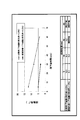
- FIG. 5 shows the relationship between the difference in the porosity of the underlying film (SiO 2 film) and the difference in the time-series change in the contact angle of the water droplets adhering to the hydrophilic film 111.
- the porosity of the base film 122 of this embodiment is 1.5%
- the porosity of the base film of the comparative example is a 2.8% film.
- the configuration of the multilayer film of this embodiment used in this experiment is the same as that shown in FIG.
- the structure of the multilayer film according to the comparative example is shown in FIG.
- n the known refractive index of the material used for the hydrophilic film
- n (V) the refractive index in vacuum of the hydrophilic film formed in this experiment.
- the refractive index in vacuum was determined by measuring the reflectance during film formation using an optical film thickness meter in a vacuum-deposited film formation chamber and converting it to a refractive index.
- the filling rate of the hydrophilic film can be expressed as follows.
- the physical film thickness was measured using a cross-sectional TEM photograph.
- the optical film thickness nd can be obtained by the refractive index n ⁇ physical film thickness d shown in the table.
- the refractive index of each layer was calculated from the reflectance of the film (corresponding to the refractive index of the film in the atmosphere). Specifically, the reflectivity of the substrate taken out into the atmosphere was measured with a microscope type spectrophotometer (USPM-RU3) manufactured by Olympus Corporation, and converted into a refractive index.
- the refractive index is at a wavelength of 550 nm.
- the water droplet extension speed is faster when the SiO 2 film with a porosity of 1.5% is used as the base film than when the SiO 2 film with the porosity of 2.8% is used as the base film (ie, contact It can be seen that the corner becomes smaller in a shorter time).
- the water droplet extension speed depends on the physical film thickness of the hydrophilic film 111 in addition to the porosity of the base film 122.
- FIG. 7 shows the relationship between the physical film thickness of the hydrophilic film 111 and the contact angle of the water droplet after a certain time from when the water droplet was dropped.
- the experiment of FIG. 7 was performed by changing the physical film thickness of the hydrophilic film 111 based on the film configuration shown in FIG. As described above, the physical film thickness was measured using the cross-sectional TEM photograph.
- the hydrophilic film 111 the faster the water droplet extension speed (the smaller the contact angle after 5 seconds). Specifically, the smaller the physical film thickness of the hydrophilic film 111, the smaller the amount of water for the hydrophilic film 111 to become a water retention layer, and therefore the hydrophilic film 111 tends to become a water retention layer. In the state where the hydrophilic film 111 is a water retention layer, the hydrophilic film 111 is optically uniform like a water surface, and has low light scattering and refraction and high transmittance.
- the change in the design center reflectance (reflectance at a predetermined wavelength) when absorbed is small, and the predetermined reflectance is achieved.
- the wavelength shift amount on the long wavelength side is small (this point will be described later).
- the physical film thickness of the hydrophilic film 111 is preferably 0.5 nm or more and 20 nm or less, more preferably 10 nm or more and 15 nm or less, and most preferably 15 nm considering the film strength.
- the hydrophilic film 111 according to the embodiment is super hydrophilic.
- the SiO 2 film is employed as the hydrophilic film 111.
- FIGS. It is thought that the tendency explained in the above appears.
- the refractive index fluctuation is reduced before and after the hydrophilic film 111 becomes a water retention layer, and a dense film is formed under the hydrophilic film 111.
- the base film 122 moisture can be prevented from entering the base film 122 and the antireflection film 121 provided thereunder, and a decrease in antireflection performance can be suppressed.
- FIG. 8 shows the first spectral reflectance characteristic of the optical lens 100 (the physical film thickness of the hydrophilic film 111 is 10 nm) and the second spectral reflectance characteristic of the optical lens 100 (the physical film thickness of the hydrophilic film 111 is 50 nm).
- the configuration of the multilayer film of this embodiment used in this experiment is the same as that shown in FIG.
- the structure of the multilayer film according to the comparative example is shown in FIG.
- the spectral reflectance measured in the experiment of FIG. 8 was measured with a microscope type spectrophotometer (USPM-RU3) manufactured by Olympus Corporation.
- the graph (A) shows the first spectral reflectance characteristic, that is, the spectral reflectance characteristic of the optical lens 100 in which the physical film thickness of the hydrophilic film 111 is 10 nm
- the graph (B) shows the second spectral reflectance.
- 3 shows a rate characteristic, that is, a spectral reflectance characteristic of the optical lens 100 in which the physical film thickness of the hydrophilic film 111 is 50 nm.
- the smaller the physical film thickness of the hydrophilic film 111, the smaller the change ⁇ Rc in the design center reflectance (reflectance at the wavelength ⁇ 550 nm), and It can be seen that the wavelength shift amount ⁇ on the long wavelength side with a reflectance of 1% is small.
- the “wavelength shift amount” is the amount of change between the spectral characteristics before heating (for example, at room temperature) and the spectral characteristics after heating.
- At least one of the hydrophilic film 111 and the base film 122 is composed of a single substance of SiO 2 , ZrO 2 , Al 2 O 3 , TiO 2 , Ti 3 O 5 , Ta 2 O 5 and Nb 2 O 5 or these. It can be a mixed material.
- the present invention is an optical element other than an optical lens, such as a mirror (reflective optical element), a filter, an array-shaped optical element (lens array, prism array), a finder element, a diffractive optical element, a Fresnel lens, and the like. It is also applicable to.
- the surface of an optical element such as an optical lens (surface on which an optical thin film is formed) may be spherical or aspherical.
- the base film may also serve as an antireflection film.
- the multilayer film may be two layers of a hydrophilic film and a base film that also serves as an antireflection film.
- the multilayer film can be applied to an optical element in an environment where high antireflection performance is not required, such as a lens for a camera having a lower performance than an in-vehicle camera or a surveillance camera, or a door mirror.
- the configuration of the multilayer film is not limited to the configuration illustrated in FIG. 3, and for example, the configuration illustrated in FIGS. 10, 11, and 12 may be used.
Landscapes
- Chemical & Material Sciences (AREA)
- Chemical Kinetics & Catalysis (AREA)
- Engineering & Computer Science (AREA)
- Materials Engineering (AREA)
- Mechanical Engineering (AREA)
- Metallurgy (AREA)
- Organic Chemistry (AREA)
- Physics & Mathematics (AREA)
- Inorganic Chemistry (AREA)
- General Physics & Mathematics (AREA)
- Optics & Photonics (AREA)
- Health & Medical Sciences (AREA)
- Toxicology (AREA)
- Surface Treatment Of Optical Elements (AREA)
- Laminated Bodies (AREA)
- Physical Vapour Deposition (AREA)
Abstract
親水性と反射防止機能の両方を有する光学薄膜を提供する。光学薄膜としての多層膜(102)において、最上層の膜が、多孔質の膜である親水性膜(111)である。最上層の次の膜が、緻密質の膜である下地膜(122)である。親水性膜(111)の気孔率は、2%以上20%以下であり、親水性膜(111)の物理膜厚は、0.5nm以上20nm以下である。下地膜(122)の気孔率は、2%未満である。
Description
本発明は、概して、光学薄膜に関する。
光学素子の一例として、スチルカメラやビデオカメラのようなカメラに搭載される光学レンズ(例えばガラスレンズ)がある。レンズ表面に水滴(例えばミスト)が付着している状態で撮像すると、撮像画像の品質が劣化することが知られている。
この問題の解決策として、特許文献1に開示の親水性の膜をカメラ用のレンズに形成することが考えられる。
カメラ用のレンズには、一般に、透過率を上げて撮像画像の品質を向上するために反射防止膜が形成されている。このため、特許文献1に開示の親水性膜をカメラ用のレンズに形成するということは、そのような親水性膜を光学レンズの反射防止膜上に形成することになる。
しかし、単純に反射防止膜上に親水性膜を形成すると、親水性が十分に得られなかったり、吸湿により反射防止膜の屈折率が変化するため反射防止機能が損なわれたりする(例えば反射率特性が低下する)おそれがある。反射防止機能が損なわれると、撮像画像の品質が劣化、具体的には、撮像画像にゴースト及び色むらの少なくとも一方が生じる。撮像画像の品質の劣化は、画像処理に悪影響を与える。これは、特に、車載カメラや監視カメラが行うセンシング処理や認識処理(典型的には人又は物体を認識する処理)のような高度な画像処理にとっては大きな問題である。
この種の問題は、光学レンズ以外の光学素子上の光学薄膜についてもあり得る。
また、特許文献1に開示の光学薄膜は、多層膜であり、最上層の膜が、表面に凹凸を有する親水性の膜であり、最上層の次の膜が、光触媒反応を呈する膜である。本願発明者の考察によれば、このような多層膜では、期待される親水性は得られない。
本発明の一実施形態の目的は、親水性と反射防止機能の両方を有する光学薄膜を提供することにある。
本発明の一実施形態に係る光学薄膜は、多層膜である。多層膜において、最上層の膜が、多孔質の膜である親水性膜である。最上層の次の膜が、緻密質の膜である下地膜である。
親水性膜の気孔率は、2%以上20%以下であり、親水性膜の物理膜厚は、0.5nm以上20nm以下である。下地膜の気孔率は、2%未満である。
本発明の一実施形態によれば、親水性と反射防止機能の両方を有する光学薄膜を提供できる。
以下、本発明の幾つかの実施形態に係る光学レンズを説明する。なお、以下に説明する実施形態は特許請求の範囲にかかる発明を限定するものではなく、また実施形態の中で説明されている諸要素及びその組み合わせの全てが発明の解決手段に必須であるとは限らない。
図1は、本発明の実施形態に係る光学レンズの構成の概念を示す。
光学レンズ100は、光学レンズ本体101と、光学レンズ本体101の表面上に形成された光学薄膜である多層膜102とを備える。多層膜102は、重なり合った(階層的な)複数の膜である。
多層膜102は、親水性と反射防止機能の両方を有する。多層膜102において、第1の層(最上位層)の膜が、多孔質の膜である親水性膜111である。第2の層(最上位層の次の層)の膜が、緻密質の膜である下地膜122である。第1及び第2の層以外の層の膜が、反射防止機能を有する1又は複数の膜で構成される反射防止膜121である。
下地膜122は、親水性膜111と反射防止膜121との間に位置する。光学的には、多層膜102を付した光学レンズ100の全体で所望の分光反射率を有するように各層の屈折率及び物理膜厚が決定される。
図2は、親水性膜111及び下地膜122の機能を説明する模式図である。なお、以下の説明では、便宜上、光学レンズ100の向きに関わらず、光学レンズ本体101側の層を「下層」と言い、光学レンズ100の表面側(光学レンズ本体101側と反対側)の層を「上層」と言い、上下方向(膜の重なりの方向)と鉛直の方向を「水平方向」と言う。
親水性膜111は、上述したように多孔質の膜であり、毛細管現象により雰囲気中の水滴を吸湿できる。親水性膜111の気孔率は、2%以上20%以下である。親水性膜111の物理膜厚は、0.5nm(ナノメートル)以上20nm以下である。
下地膜122は、気孔率が2%未満の緻密な膜であり、親水性膜111から下層への水の進みを妨げる(遮断する)。これにより、親水性膜111により吸湿された水分が、親水性膜111から下地膜122内に進入することが困難のため、親水性膜111にて水分が保持され、結果として、親水性膜111が保水層となる。
以下、親水性膜111が保水層になるまでの流れを説明する。
図2の(A)に示すように、親水性膜111に十分な水分が無い状態において、(B)に示すように、水滴281が親水性膜111表面に付着すると、(C)に示すように、毛細管現象により水滴281が親水性膜111により吸湿され、(D)に示すように、水滴281は、比較的長い時間(例えば数十秒~数分)をかけて、親水性膜111に吸湿されながら伸展する。本実施形態において、親水性膜111における水滴の伸展とは、水平方向への水滴の拡がり、具体的には、親水性膜111に付着した水滴の接触角が、最大接触角(例えば静的接触角)から最小接触角になることを意味する。
単位時間あたりに親水性膜111表面に付着する水滴の量が少ないと(例えば低湿度環境では)、(A)~(D)の流れが繰り返されると考えられる。なぜなら、親水性膜111に保持される水の量よりも雰囲気中に蒸発する水の量の方が多い等の原因により、親水性膜111は保水層とならないと考えられるためである。
しかし、(E)に示すように(例えば高湿度環境のように)、単位時間あたりに親水性膜111表面に付着する水滴281の量が多い(蒸発する水の量より保持される水の量の方が多い)と、(F)に示すように、親水性膜111が保水層Wとなる。なぜなら、親水性膜111に吸湿された水の下層への進みは下地膜122により遮断され、結果として、親水性膜111に水分が保持されるためである。
(G)に示すように、保水層Wとなっている親水性膜111に付着した水滴281は、短時間(例えば5秒以下)で伸展が完了することになる。なぜなら、多孔質膜内の孔が既に水で満たされており、その水に水滴281が一体化するように拡がるためである。
また、実施形態によれば、親水性膜111の物理膜厚は、小さく、具体的には、上述したように、0.5nm(ナノメートル)以上20nm以下である。これにより、吸湿しても反射率特性の変化は少ない。親水性膜111の物理膜厚は、下地膜122の物理膜厚より薄くてよい。
また、実施形態によれば、上述したように、親水性膜111の次の膜が、気孔率が2%未満といった緻密な下地膜122であり、下地膜122内への水の進入が遮断される。このため、屈折率変化が少ない。結果として、反射率特性の変化が少ない。
なお、光学的には、親水性膜111と下地膜122とを含んだ全体で所望の反射防止特性を得るように、多層膜102における各膜の材料及び物理膜厚が選択される。
図3は、実施形態に係る多層膜102の構成を示す。以下の説明では、層番号X(X番目の層)の膜を「膜X」と表記する。層番号Xの値が小さい膜ほど下層の膜である。Xの最小値は1であり、膜1が最下層の膜である。
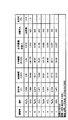
多層膜102は、8つの膜から構成される。反射防止膜121が、膜1~膜6であり、下地膜122が、膜7であり、親水性膜111が、膜8である。
実施形態では、EB(電子ビーム)蒸着により形成されたSiO2膜が、親水性膜111(膜8)である。IAD(イオンアシスト蒸着)により形成されたSiO2膜が、下地膜122(膜7)である。
図4は、実施形態に係る光学薄膜形成システムを示す。
光学薄膜形成システム301は、IADにより膜を形成するIAD装置311と、EB蒸着により膜を形成するEB蒸着装置312とを備え、光学薄膜形成方法を実行する。
IADは、イオン銃から基板に照射されるイオン化されたガス分子により蒸着材料分子を基板に押し付ける成膜方法である。そのため、IADにより、水分子の入り込む隙間のない程に緻密性の高い膜の形成が可能であると考えられる。そこで、本実施形態では、下地膜122として、IADにより形成された膜(例えばSiO2膜)が採用される。
EB蒸着は、電子を蒸着材料の一部分に集中してぶつけて加熱し蒸発させて行う成膜方法である。そのため、EB蒸着により、多孔質膜としての親水性膜111の形成が可能であると考えられる。そこで、本実施形態では、親水性膜111として、EB蒸着により形成された膜(例えばSiO2膜)が採用される。
なお、図4に示すシステムに従う成膜方法は、好ましい成膜方法の一例である。成膜方法は、図4に示す例に限られない。例えば、下地膜122は、IAD以外の方法で成膜されてもよいし、親水性膜111は、EB蒸着以外の方法で成膜されてもよい。
また、親水性膜111及び下地膜122のいずれも、SiO2以外の材料で構成された膜でもよいが、本実施形態のように、SiO2という、光学薄膜としては一般的な材料が使用されるので、多層膜102が形成された光学素子の量産に有利である。本実施形態では、最上層の膜の物理膜厚及び気孔率の工夫と、最上層の次の層の膜の気孔率の工夫との組合せにより、最上層の膜を保水層とすること(親水性)、及び、反射率特性の変化を抑えること(反射防止機能)の両方を実現することができる。
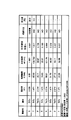
図5は、下地膜(SiO2膜)の気孔率の違いと親水性膜111に付着した水滴の接触角の時系列変化の違いとの関係を示す。本実施形態の下地膜122の気孔率は、1.5%であり、比較例の下地膜の気孔率は2.8%膜である。なお、この実験で使用した本実施形態の多層膜の構成は、図3と同じである。また、比較例に係る多層膜の構成は、図6に示されている。
ここで、気孔率の算出方法について説明する。まず、親水性膜に使用される材質の既知の屈折率をnとし、本実験にて成膜された親水性膜の真空中の屈折率をn(V)とする。真空中の屈折率は、真空保持された成膜チャンバ内にて光学膜厚計を使用して、成膜中の反射率を測定し、屈折率に換算して求めた。親水性膜の充填率は、以下のように表すことができる。
充填率(%)=[真空中の屈折率(%)/既知の屈折率(%)]×100(%)
したがって、気孔率は、
気孔率(%)=100(%)-充填率(%)
として求めることができる。
したがって、気孔率は、
気孔率(%)=100(%)-充填率(%)
として求めることができる。
また、物理膜厚は、断面TEM写真を用いて測定した。また、光学膜厚ndは、表に示す屈折率n×物理膜厚dで求めることができる。各層の屈折率は、膜の反射率から換算して求めた(大気中の膜の屈折率に該当)。具体的には、大気中に取り出した基板を、オリンパス(株)製の顕微鏡型分光測定機(USPM―RU3)にて反射率を測定し、屈折率に換算して求めた。なお、屈折率は、波長550nmにおけるものである。光学膜厚係数kは、基準波長λ0=550nmにおける係数であり、光学膜厚nd=k×λ0/4である。
図5によれば、気孔率2.8%のSiO2膜を下地膜とするよりも気孔率1.5%のSiO2膜を下地膜とする方が、水滴伸展速度が速い(すなわち、接触角がより短時間で小さくなる)ことがわかる。
水滴伸展速度は、下地膜122の気孔率に加えて、親水性膜111の物理膜厚にも依存する。
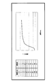
図7は、親水性膜111の物理膜厚と水滴が滴下されてから一定時間後の水滴の接触角との関係を示す。図7の実験は、図3に示す膜構成を基に、親水性膜111の物理膜厚を変化させて行った。物理膜厚の測定は、上記したように、断面TEM写真を用いて行った。
実験では、サンプル表面に純水を0.8μl液下し、5秒後の接触角θを求めた。
図7によれば、親水性膜111の物理膜厚が小さいほど、水滴伸展速度が速い(5秒後の接触角度が小さい)。具体的には、親水性膜111の物理膜厚が小さいほど、親水性膜111が保水層になるための水分量が少なく、故に、親水性膜111が保水層になり易い。親水性膜111が保水層の状態では、親水性膜111が水面のように光学的に均一となり、光の散乱や屈折が少なく透過率が高い。その他、親水性膜111の物理膜厚が小さいと、光学レンズ100の分光反射率特性において、吸水したときの設計中心反射率(所定波長での反射率)の変化が小さく、且つ、所定反射率での長波長側の波長シフト量が小さい(この点は後に説明する)。
図7によれば、親水性膜111の物理膜厚は、0.5nm以上20nm以下が望ましく、膜強度を考慮すると、より望ましくは、10nm以上15nm以下、最も望ましくは、15nmである。
なお、図7によれば、滴下から一定時間後の接触角が10°未満であることから、実施形態に係る親水性膜111は、超親水性であると言える。また、実施形態では、親水性膜111としてSiO2膜が採用されているが、他種の膜材により形成された膜が親水性膜111として採用されても、図5及び図7を参照して説明した傾向が表れると考えられる。
また、実施形態では、親水性膜111の物理膜厚を小さくすることで、親水性膜111が保水層になる前後で屈折率変動を小さくし、且つ、親水性膜111の下に緻密質の下地膜122を設けることで、下地膜122及びその下に設けた反射防止膜121に水分が入ることを防ぎ、反射防止性能の低下が抑えられる。
図8は、光学レンズ100の第1の分光反射率特性(親水性膜111の物理膜厚が10nm)と、光学レンズ100の第2の分光反射率特性(親水性膜111の物理膜厚が50nm)とを示す。なお、この実験で使用した本実施形態の多層膜の構成は、図3と同じである。また、比較例に係る多層膜の構成は、図9に示されている。
図8の実験で測定した分光反射率は、オリンパス(株)製の顕微鏡型分光測定機(USPM―RU3)により測定した。
グラフ(A)が、第1の分光反射率特性、すなわち、親水性膜111の物理膜厚が10nmである光学レンズ100の分光反射率特性を示し、グラフ(B)が、第2の分光反射率特性、すなわち、親水性膜111の物理膜厚が50nmである光学レンズ100の分光反射率特性を示す。グラフ(A)とグラフ(B)の対比によれば、親水性膜111の物理膜厚が小さい方が、設計中心反射率(波長λ=550nmでの反射率)の変化ΔRcが小さく、且つ、反射率1%での長波長側の波長シフト量Δλが小さいことがわかる。「波長シフト量」とは、加熱前(例えば常温時)の分光特性と、加熱後の分光特性との変化量である。
以上、本発明の一実施形態を説明したが、これは、本発明の説明のための例示であって、本発明の範囲をこの実施形態にのみ限定する趣旨ではない。すなわち、本発明は、他の種々の形態でも実施する事が可能である。
例えば、親水性膜111及び下地膜122の少なくとも一方は、SiO2、ZrO2、Al2O3、TiO2、Ti3O5、Ta2O5及びNb2O5のうちの単体若しくはこれらを含む混合材とすることができる。
また、例えば、本発明は、光学レンズ以外の光学素子、例えば、ミラー(反射型光学素子)、フィルター、アレー状光学素子(レンズアレー、プリズムアレー)、ファインダー素子、回折型光学素子、フレネルレンズなどにも適用可能である。また、光学レンズのような光学素子の表面(光学薄膜が形成される面)は、球面でも非球面でもよい。
また、例えば、下地膜が、反射防止膜を兼ねてもよい。つまり、多層膜は、親水膜と、反射防止膜と兼ねた下地膜との2層でもよい。その多層膜は、車載カメラや監視カメラよりも性能の低いカメラ向けのレンズや、ドアミラーのように、高い反射防止性能が要求されない環境での光学素子に適用することができる。
また、多層膜の構成は、図3に例示の構成に限らず、例えば、図10、図11及び図12に例示の構成でもよい。
本出願は、2017年4月14日出願の特願2017-080463に基づく。この内容は全てここに含めておく。
Claims (6)
- 光学素子本体と、
前記光学素子本体の表面上に形成された多層膜である光学薄膜とを備え、
前記光学薄膜において、
最上層の膜が、多孔質の膜である親水性膜であり、
前記最上層の次の膜が、緻密質の膜である下地膜であり、
前記親水性膜の気孔率は、2%以上20%以下であり、
前記親水性膜の物理膜厚は、0.5nm以上20nm以下であり、
前記下地膜の気孔率は、2%未満である、
光学素子。 - 前記親水性膜及び前記下地膜の少なくとも一方は、SiO2、ZrO2、Al2O3、TiO2、Ti3O5、Ta2O5及びNb2O5のうちの単体若しくはこれらを含む混合材である、
請求項1記載の光学素子。 - 前記親水性膜が、SiO2膜である、
請求項2記載の光学素子。 - 前記下地膜が、SiO2膜である、
請求項2又は3記載の光学素子。 - 前記親水性膜が、EB(電子ビーム)蒸着により形成された膜であり、
前記下地膜が、IAD(イオンアシスト蒸着)により形成された膜である、請求項1乃至3のうちのいずれか1項に記載の光学素子。 - 多層膜である光学薄膜であって、
最上層の膜が、多孔質の膜である親水性膜であり、
前記最上層の次の膜が、緻密質の膜である下地膜であり、
前記親水性膜の気孔率は、2%以上20%以下であり、
前記親水性膜の物理膜厚は、0.5nm以上20nm以下であり、
前記下地膜の気孔率は、2%未満である、
光学薄膜。
Priority Applications (2)
| Application Number | Priority Date | Filing Date | Title |
|---|---|---|---|
| CN201880024875.1A CN110691995B (zh) | 2017-04-14 | 2018-04-13 | 光学元件以及光学薄膜 |
| JP2019512571A JP7091315B2 (ja) | 2017-04-14 | 2018-04-13 | 光学素子及びその製造方法 |
Applications Claiming Priority (2)
| Application Number | Priority Date | Filing Date | Title |
|---|---|---|---|
| JP2017080463 | 2017-04-14 | ||
| JP2017-080463 | 2017-04-14 |
Publications (1)
| Publication Number | Publication Date |
|---|---|
| WO2018190408A1 true WO2018190408A1 (ja) | 2018-10-18 |
Family
ID=63793341
Family Applications (1)
| Application Number | Title | Priority Date | Filing Date |
|---|---|---|---|
| PCT/JP2018/015466 Ceased WO2018190408A1 (ja) | 2017-04-14 | 2018-04-13 | 光学素子及び光学薄膜 |
Country Status (3)
| Country | Link |
|---|---|
| JP (1) | JP7091315B2 (ja) |
| CN (1) | CN110691995B (ja) |
| WO (1) | WO2018190408A1 (ja) |
Cited By (2)
| Publication number | Priority date | Publication date | Assignee | Title |
|---|---|---|---|---|
| WO2021261225A1 (ja) * | 2020-06-23 | 2021-12-30 | コニカミノルタ株式会社 | 親水性膜の製造方法、親水性膜及び光学部材 |
| KR20230163965A (ko) * | 2020-12-10 | 2023-12-01 | 정인용 | 코팅 렌즈의 제조 방법 |
Citations (4)
| Publication number | Priority date | Publication date | Assignee | Title |
|---|---|---|---|---|
| WO2004108283A1 (ja) * | 2003-06-09 | 2004-12-16 | Nippon Sheet Glass Co., Ltd. | 光触媒部材 |
| JP2012237941A (ja) * | 2011-05-13 | 2012-12-06 | Asahi Glass Co Ltd | 光学部品、光学装置 |
| US20140178657A1 (en) * | 2012-12-21 | 2014-06-26 | Intermolecular Inc. | Antireflection coatings |
| JP2016001200A (ja) * | 2012-10-15 | 2016-01-07 | 旭硝子株式会社 | 防汚性反射防止膜、物品およびその製造方法 |
Family Cites Families (5)
| Publication number | Priority date | Publication date | Assignee | Title |
|---|---|---|---|---|
| JP3540884B2 (ja) * | 1996-02-07 | 2004-07-07 | 日東電工株式会社 | 膜構造材の製造方法 |
| DE69930399T2 (de) * | 1998-09-30 | 2006-12-07 | Nippon Sheet Glass Co., Ltd. | Photokatalysatorartikel mit verhinderung von verstopfungen und ablagerungen, verfahren zur herstellung des artikels |
| CN1401086A (zh) * | 2001-06-11 | 2003-03-05 | 株式会社村上开明堂 | 防雾元件及其形成方法 |
| JP5266019B2 (ja) * | 2008-11-10 | 2013-08-21 | 学校法人慶應義塾 | 反射防止膜、その形成方法、光学素子、交換レンズ及び撮像装置 |
| CN105143357B (zh) * | 2012-09-26 | 2019-02-22 | 3M创新有限公司 | 可涂覆型组合物、防污组合物、防污制品以及制备它们的方法 |
-
2018
- 2018-04-13 WO PCT/JP2018/015466 patent/WO2018190408A1/ja not_active Ceased
- 2018-04-13 CN CN201880024875.1A patent/CN110691995B/zh active Active
- 2018-04-13 JP JP2019512571A patent/JP7091315B2/ja active Active
Patent Citations (4)
| Publication number | Priority date | Publication date | Assignee | Title |
|---|---|---|---|---|
| WO2004108283A1 (ja) * | 2003-06-09 | 2004-12-16 | Nippon Sheet Glass Co., Ltd. | 光触媒部材 |
| JP2012237941A (ja) * | 2011-05-13 | 2012-12-06 | Asahi Glass Co Ltd | 光学部品、光学装置 |
| JP2016001200A (ja) * | 2012-10-15 | 2016-01-07 | 旭硝子株式会社 | 防汚性反射防止膜、物品およびその製造方法 |
| US20140178657A1 (en) * | 2012-12-21 | 2014-06-26 | Intermolecular Inc. | Antireflection coatings |
Cited By (3)
| Publication number | Priority date | Publication date | Assignee | Title |
|---|---|---|---|---|
| WO2021261225A1 (ja) * | 2020-06-23 | 2021-12-30 | コニカミノルタ株式会社 | 親水性膜の製造方法、親水性膜及び光学部材 |
| KR20230163965A (ko) * | 2020-12-10 | 2023-12-01 | 정인용 | 코팅 렌즈의 제조 방법 |
| KR102719055B1 (ko) * | 2020-12-10 | 2024-10-17 | 정인용 | 코팅 렌즈의 제조 방법 |
Also Published As
| Publication number | Publication date |
|---|---|
| CN110691995A (zh) | 2020-01-14 |
| JPWO2018190408A1 (ja) | 2020-03-05 |
| CN110691995B (zh) | 2021-11-26 |
| JP7091315B2 (ja) | 2022-06-27 |
Similar Documents
| Publication | Publication Date | Title |
|---|---|---|
| US9158039B2 (en) | Optical element, and optical system and optical apparatus using same | |
| US8226250B2 (en) | Optical element and optical system | |
| US9302450B2 (en) | Optical element, optical system, and optical apparatus | |
| JP2015004919A (ja) | 反射防止膜及びそれを有する光学素子 | |
| JP2003050311A (ja) | 紫外線用の減衰フィルタ | |
| WO2016031133A1 (ja) | 反射防止膜を備えた光学部材およびその製造方法 | |
| JP2014021146A (ja) | 光学膜、光学素子、光学系および光学機器 | |
| JP2007507753A (ja) | 区分空洞波長可変ファブリ・ペロ・フィルタ | |
| US10459123B2 (en) | Optical member, image pickup apparatus, and method for manufacturing optical member | |
| WO2016031167A1 (ja) | 反射防止膜および反射防止膜を備えた光学部材 | |
| JP7091315B2 (ja) | 光学素子及びその製造方法 | |
| US20200308415A1 (en) | Optical member, optical device and coating liquid | |
| US10644048B2 (en) | Anti-reflective coating with high refractive index material at air interface | |
| EP3373048B1 (en) | Optical member, image pickup apparatus, and method for manufacturing optical member | |
| JP6989289B2 (ja) | 親水性反射防止膜付きレンズ及びその製造方法 | |
| JP2004205777A (ja) | 光学フィルタの製造方法 | |
| JP2010066704A (ja) | 光学素子、光学系及び光学機器 | |
| JP2010048896A (ja) | 光学系 | |
| CN102575340A (zh) | 光学部件的制造方法和光学部件 | |
| WO2021024834A1 (ja) | 反射防止膜付き光学部材及びその製造方法 | |
| JP2004212462A (ja) | 光量絞り用ndフィルタ、光量絞り装置、該光量絞り装置を有するカメラ、フィルタの製造方法 | |
| JP6714399B2 (ja) | 光学素子及び光学薄膜の成膜方法 | |
| JP2004333908A (ja) | 反射防止膜を有する光学素子 | |
| JP7378924B2 (ja) | 光学素子、その製造方法、撮像装置、および光学機器 | |
| JP2006330128A (ja) | Irカット膜付きndフィルタ、irカット膜付きndフィルタの製造方法、及びこれらのndフィルタを有する光量絞り装置及びカメラ |
Legal Events
| Date | Code | Title | Description |
|---|---|---|---|
| 121 | Ep: the epo has been informed by wipo that ep was designated in this application |
Ref document number: 18784846 Country of ref document: EP Kind code of ref document: A1 |
|
| ENP | Entry into the national phase |
Ref document number: 2019512571 Country of ref document: JP Kind code of ref document: A |
|
| NENP | Non-entry into the national phase |
Ref country code: DE |
|
| 122 | Ep: pct application non-entry in european phase |
Ref document number: 18784846 Country of ref document: EP Kind code of ref document: A1 |