WO2018186320A1 - Ébauche de masque, procédé de fabrication de masque de transfert et procédé de fabrication de dispositif à semi-conducteurs - Google Patents
Ébauche de masque, procédé de fabrication de masque de transfert et procédé de fabrication de dispositif à semi-conducteurs Download PDFInfo
- Publication number
- WO2018186320A1 WO2018186320A1 PCT/JP2018/014039 JP2018014039W WO2018186320A1 WO 2018186320 A1 WO2018186320 A1 WO 2018186320A1 JP 2018014039 W JP2018014039 W JP 2018014039W WO 2018186320 A1 WO2018186320 A1 WO 2018186320A1
- Authority
- WO
- WIPO (PCT)
- Prior art keywords
- film
- pattern
- mask
- etching stopper
- etching
- Prior art date
Links
- 238000012546 transfer Methods 0.000 title claims description 176
- 238000004519 manufacturing process Methods 0.000 title claims description 50
- 239000004065 semiconductor Substances 0.000 title claims description 33
- 238000005530 etching Methods 0.000 claims abstract description 391
- 239000000463 material Substances 0.000 claims abstract description 131
- VYZAMTAEIAYCRO-UHFFFAOYSA-N Chromium Chemical compound [Cr] VYZAMTAEIAYCRO-UHFFFAOYSA-N 0.000 claims abstract description 115
- 239000011651 chromium Substances 0.000 claims abstract description 115
- 229910052804 chromium Inorganic materials 0.000 claims abstract description 109
- 239000000758 substrate Substances 0.000 claims abstract description 90
- 238000001228 spectrum Methods 0.000 claims abstract description 83
- 238000004458 analytical method Methods 0.000 claims abstract description 64
- 229910052760 oxygen Inorganic materials 0.000 claims abstract description 50
- 239000001301 oxygen Substances 0.000 claims abstract description 46
- 229910052799 carbon Inorganic materials 0.000 claims abstract description 45
- QVGXLLKOCUKJST-UHFFFAOYSA-N atomic oxygen Chemical compound [O] QVGXLLKOCUKJST-UHFFFAOYSA-N 0.000 claims abstract description 44
- 238000004833 X-ray photoelectron spectroscopy Methods 0.000 claims abstract description 43
- OKTJSMMVPCPJKN-UHFFFAOYSA-N Carbon Chemical compound [C] OKTJSMMVPCPJKN-UHFFFAOYSA-N 0.000 claims abstract description 42
- 229910052710 silicon Inorganic materials 0.000 claims abstract description 37
- 239000010703 silicon Substances 0.000 claims abstract description 34
- GUVRBAGPIYLISA-UHFFFAOYSA-N tantalum atom Chemical compound [Ta] GUVRBAGPIYLISA-UHFFFAOYSA-N 0.000 claims abstract description 25
- 229910052715 tantalum Inorganic materials 0.000 claims abstract description 24
- 238000001514 detection method Methods 0.000 claims abstract description 20
- 239000010408 film Substances 0.000 claims description 727
- 239000007789 gas Substances 0.000 claims description 136
- 238000001312 dry etching Methods 0.000 claims description 134
- 230000010363 phase shift Effects 0.000 claims description 82
- MYMOFIZGZYHOMD-UHFFFAOYSA-N Dioxygen Chemical compound O=O MYMOFIZGZYHOMD-UHFFFAOYSA-N 0.000 claims description 47
- 239000000460 chlorine Substances 0.000 claims description 47
- 229910001882 dioxygen Inorganic materials 0.000 claims description 47
- 239000010409 thin film Substances 0.000 claims description 45
- 238000000034 method Methods 0.000 claims description 41
- ZAMOUSCENKQFHK-UHFFFAOYSA-N Chlorine atom Chemical compound [Cl] ZAMOUSCENKQFHK-UHFFFAOYSA-N 0.000 claims description 31
- 229910052801 chlorine Inorganic materials 0.000 claims description 31
- YCKRFDGAMUMZLT-UHFFFAOYSA-N Fluorine atom Chemical compound [F] YCKRFDGAMUMZLT-UHFFFAOYSA-N 0.000 claims description 22
- 229910052731 fluorine Inorganic materials 0.000 claims description 22
- 239000011737 fluorine Substances 0.000 claims description 22
- 239000000470 constituent Substances 0.000 claims description 12
- 230000007261 regionalization Effects 0.000 claims description 9
- 230000008569 process Effects 0.000 claims description 7
- IJGRMHOSHXDMSA-UHFFFAOYSA-N Atomic nitrogen Chemical compound N#N IJGRMHOSHXDMSA-UHFFFAOYSA-N 0.000 description 52
- 230000000052 comparative effect Effects 0.000 description 49
- 238000004544 sputter deposition Methods 0.000 description 35
- XUIMIQQOPSSXEZ-UHFFFAOYSA-N Silicon Chemical compound [Si] XUIMIQQOPSSXEZ-UHFFFAOYSA-N 0.000 description 31
- 239000000126 substance Substances 0.000 description 31
- 229910052757 nitrogen Inorganic materials 0.000 description 30
- XKRFYHLGVUSROY-UHFFFAOYSA-N Argon Chemical compound [Ar] XKRFYHLGVUSROY-UHFFFAOYSA-N 0.000 description 20
- KZBUYRJDOAKODT-UHFFFAOYSA-N Chlorine Chemical compound ClCl KZBUYRJDOAKODT-UHFFFAOYSA-N 0.000 description 19
- 239000010410 layer Substances 0.000 description 19
- 239000012528 membrane Substances 0.000 description 18
- 125000004429 atom Chemical group 0.000 description 13
- 239000002210 silicon-based material Substances 0.000 description 13
- 230000000704 physical effect Effects 0.000 description 12
- 229910016006 MoSi Inorganic materials 0.000 description 11
- 238000006243 chemical reaction Methods 0.000 description 11
- 238000010894 electron beam technology Methods 0.000 description 11
- CURLTUGMZLYLDI-UHFFFAOYSA-N Carbon dioxide Chemical compound O=C=O CURLTUGMZLYLDI-UHFFFAOYSA-N 0.000 description 10
- 229910019590 Cr-N Inorganic materials 0.000 description 10
- 229910019588 Cr—N Inorganic materials 0.000 description 10
- 229910052786 argon Inorganic materials 0.000 description 10
- 229910052723 transition metal Inorganic materials 0.000 description 10
- 150000003624 transition metals Chemical class 0.000 description 10
- 239000001307 helium Substances 0.000 description 9
- 229910052734 helium Inorganic materials 0.000 description 9
- SWQJXJOGLNCZEY-UHFFFAOYSA-N helium atom Chemical compound [He] SWQJXJOGLNCZEY-UHFFFAOYSA-N 0.000 description 9
- 239000000203 mixture Substances 0.000 description 9
- 238000013461 design Methods 0.000 description 8
- 238000007689 inspection Methods 0.000 description 8
- 238000000059 patterning Methods 0.000 description 8
- 238000004088 simulation Methods 0.000 description 8
- ZOKXTWBITQBERF-UHFFFAOYSA-N Molybdenum Chemical compound [Mo] ZOKXTWBITQBERF-UHFFFAOYSA-N 0.000 description 7
- 229910052750 molybdenum Inorganic materials 0.000 description 7
- 239000011733 molybdenum Substances 0.000 description 7
- 238000005001 rutherford backscattering spectroscopy Methods 0.000 description 7
- 230000015572 biosynthetic process Effects 0.000 description 6
- 238000012937 correction Methods 0.000 description 6
- VYPSYNLAJGMNEJ-UHFFFAOYSA-N silicon dioxide Inorganic materials O=[Si]=O VYPSYNLAJGMNEJ-UHFFFAOYSA-N 0.000 description 6
- 238000004528 spin coating Methods 0.000 description 6
- 238000002834 transmittance Methods 0.000 description 6
- ZOXJGFHDIHLPTG-UHFFFAOYSA-N Boron Chemical compound [B] ZOXJGFHDIHLPTG-UHFFFAOYSA-N 0.000 description 5
- PXHVJJICTQNCMI-UHFFFAOYSA-N Nickel Chemical compound [Ni] PXHVJJICTQNCMI-UHFFFAOYSA-N 0.000 description 5
- 229910052796 boron Inorganic materials 0.000 description 5
- 229910002092 carbon dioxide Inorganic materials 0.000 description 5
- 239000001569 carbon dioxide Substances 0.000 description 5
- 239000011521 glass Substances 0.000 description 5
- 229910052751 metal Inorganic materials 0.000 description 5
- 230000003287 optical effect Effects 0.000 description 5
- 239000010453 quartz Substances 0.000 description 5
- 229910019819 Cr—Si Inorganic materials 0.000 description 4
- MWUXSHHQAYIFBG-UHFFFAOYSA-N Nitric oxide Chemical compound O=[N] MWUXSHHQAYIFBG-UHFFFAOYSA-N 0.000 description 4
- 238000009835 boiling Methods 0.000 description 4
- 230000008859 change Effects 0.000 description 4
- 238000010586 diagram Methods 0.000 description 4
- 229910052739 hydrogen Inorganic materials 0.000 description 4
- 239000001257 hydrogen Substances 0.000 description 4
- 239000002184 metal Substances 0.000 description 4
- 239000002356 single layer Substances 0.000 description 4
- UFHFLCQGNIYNRP-UHFFFAOYSA-N Hydrogen Chemical compound [H][H] UFHFLCQGNIYNRP-UHFFFAOYSA-N 0.000 description 3
- 235000010724 Wisteria floribunda Nutrition 0.000 description 3
- 230000003321 amplification Effects 0.000 description 3
- AHXGRMIPHCAXFP-UHFFFAOYSA-L chromyl dichloride Chemical compound Cl[Cr](Cl)(=O)=O AHXGRMIPHCAXFP-UHFFFAOYSA-L 0.000 description 3
- 238000010438 heat treatment Methods 0.000 description 3
- 238000002156 mixing Methods 0.000 description 3
- 239000010955 niobium Substances 0.000 description 3
- 238000003199 nucleic acid amplification method Methods 0.000 description 3
- 230000002093 peripheral effect Effects 0.000 description 3
- 238000000206 photolithography Methods 0.000 description 3
- 238000005546 reactive sputtering Methods 0.000 description 3
- 238000000851 scanning transmission electron micrograph Methods 0.000 description 3
- 239000010936 titanium Substances 0.000 description 3
- BVKZGUZCCUSVTD-UHFFFAOYSA-L Carbonate Chemical compound [O-]C([O-])=O BVKZGUZCCUSVTD-UHFFFAOYSA-L 0.000 description 2
- KJTLSVCANCCWHF-UHFFFAOYSA-N Ruthenium Chemical compound [Ru] KJTLSVCANCCWHF-UHFFFAOYSA-N 0.000 description 2
- RTAQQCXQSZGOHL-UHFFFAOYSA-N Titanium Chemical compound [Ti] RTAQQCXQSZGOHL-UHFFFAOYSA-N 0.000 description 2
- 150000001875 compounds Chemical class 0.000 description 2
- 238000000151 deposition Methods 0.000 description 2
- 230000008021 deposition Effects 0.000 description 2
- 238000011161 development Methods 0.000 description 2
- 230000018109 developmental process Effects 0.000 description 2
- 238000009826 distribution Methods 0.000 description 2
- 230000000694 effects Effects 0.000 description 2
- 229910052735 hafnium Inorganic materials 0.000 description 2
- VBJZVLUMGGDVMO-UHFFFAOYSA-N hafnium atom Chemical compound [Hf] VBJZVLUMGGDVMO-UHFFFAOYSA-N 0.000 description 2
- 239000012535 impurity Substances 0.000 description 2
- 238000001459 lithography Methods 0.000 description 2
- 229910052752 metalloid Inorganic materials 0.000 description 2
- 229910052759 nickel Inorganic materials 0.000 description 2
- 229910052758 niobium Inorganic materials 0.000 description 2
- GUCVJGMIXFAOAE-UHFFFAOYSA-N niobium atom Chemical compound [Nb] GUCVJGMIXFAOAE-UHFFFAOYSA-N 0.000 description 2
- QJGQUHMNIGDVPM-UHFFFAOYSA-N nitrogen group Chemical group [N] QJGQUHMNIGDVPM-UHFFFAOYSA-N 0.000 description 2
- 229910052707 ruthenium Inorganic materials 0.000 description 2
- 229910052719 titanium Inorganic materials 0.000 description 2
- 229910021350 transition metal silicide Inorganic materials 0.000 description 2
- WFKWXMTUELFFGS-UHFFFAOYSA-N tungsten Chemical compound [W] WFKWXMTUELFFGS-UHFFFAOYSA-N 0.000 description 2
- 229910052721 tungsten Inorganic materials 0.000 description 2
- 239000010937 tungsten Substances 0.000 description 2
- LEONUFNNVUYDNQ-UHFFFAOYSA-N vanadium atom Chemical compound [V] LEONUFNNVUYDNQ-UHFFFAOYSA-N 0.000 description 2
- ITWBWJFEJCHKSN-UHFFFAOYSA-N 1,4,7-triazonane Chemical compound C1CNCCNCCN1 ITWBWJFEJCHKSN-UHFFFAOYSA-N 0.000 description 1
- OAICVXFJPJFONN-UHFFFAOYSA-N Phosphorus Chemical compound [P] OAICVXFJPJFONN-UHFFFAOYSA-N 0.000 description 1
- BUGBHKTXTAQXES-UHFFFAOYSA-N Selenium Chemical compound [Se] BUGBHKTXTAQXES-UHFFFAOYSA-N 0.000 description 1
- 229910052581 Si3N4 Inorganic materials 0.000 description 1
- NINIDFKCEFEMDL-UHFFFAOYSA-N Sulfur Chemical compound [S] NINIDFKCEFEMDL-UHFFFAOYSA-N 0.000 description 1
- 229910004535 TaBN Inorganic materials 0.000 description 1
- 229910004166 TaN Inorganic materials 0.000 description 1
- 229910004158 TaO Inorganic materials 0.000 description 1
- 229910003071 TaON Inorganic materials 0.000 description 1
- ATJFFYVFTNAWJD-UHFFFAOYSA-N Tin Chemical compound [Sn] ATJFFYVFTNAWJD-UHFFFAOYSA-N 0.000 description 1
- QCWXUUIWCKQGHC-UHFFFAOYSA-N Zirconium Chemical compound [Zr] QCWXUUIWCKQGHC-UHFFFAOYSA-N 0.000 description 1
- 239000005354 aluminosilicate glass Substances 0.000 description 1
- 229910052787 antimony Inorganic materials 0.000 description 1
- WATWJIUSRGPENY-UHFFFAOYSA-N antimony atom Chemical compound [Sb] WATWJIUSRGPENY-UHFFFAOYSA-N 0.000 description 1
- 230000005540 biological transmission Effects 0.000 description 1
- 229910052797 bismuth Inorganic materials 0.000 description 1
- JCXGWMGPZLAOME-UHFFFAOYSA-N bismuth atom Chemical compound [Bi] JCXGWMGPZLAOME-UHFFFAOYSA-N 0.000 description 1
- 150000001845 chromium compounds Chemical class 0.000 description 1
- 238000000576 coating method Methods 0.000 description 1
- 239000010941 cobalt Substances 0.000 description 1
- 229910017052 cobalt Inorganic materials 0.000 description 1
- GUTLYIVDDKVIGB-UHFFFAOYSA-N cobalt atom Chemical compound [Co] GUTLYIVDDKVIGB-UHFFFAOYSA-N 0.000 description 1
- 238000001941 electron spectroscopy Methods 0.000 description 1
- 238000005516 engineering process Methods 0.000 description 1
- 238000000605 extraction Methods 0.000 description 1
- 229910052732 germanium Inorganic materials 0.000 description 1
- GNPVGFCGXDBREM-UHFFFAOYSA-N germanium atom Chemical compound [Ge] GNPVGFCGXDBREM-UHFFFAOYSA-N 0.000 description 1
- 229910052736 halogen Inorganic materials 0.000 description 1
- 150000002367 halogens Chemical class 0.000 description 1
- 150000002431 hydrogen Chemical class 0.000 description 1
- 230000006872 improvement Effects 0.000 description 1
- 238000010849 ion bombardment Methods 0.000 description 1
- 238000001659 ion-beam spectroscopy Methods 0.000 description 1
- 150000002500 ions Chemical class 0.000 description 1
- 230000001678 irradiating effect Effects 0.000 description 1
- 229910052743 krypton Inorganic materials 0.000 description 1
- DNNSSWSSYDEUBZ-UHFFFAOYSA-N krypton atom Chemical compound [Kr] DNNSSWSSYDEUBZ-UHFFFAOYSA-N 0.000 description 1
- 238000010030 laminating Methods 0.000 description 1
- 238000005259 measurement Methods 0.000 description 1
- 238000012986 modification Methods 0.000 description 1
- 230000004048 modification Effects 0.000 description 1
- 229910052754 neon Inorganic materials 0.000 description 1
- GKAOGPIIYCISHV-UHFFFAOYSA-N neon atom Chemical compound [Ne] GKAOGPIIYCISHV-UHFFFAOYSA-N 0.000 description 1
- 150000004767 nitrides Chemical class 0.000 description 1
- 229910052756 noble gas Inorganic materials 0.000 description 1
- 229910052755 nonmetal Inorganic materials 0.000 description 1
- 239000011368 organic material Substances 0.000 description 1
- 230000003647 oxidation Effects 0.000 description 1
- 238000007254 oxidation reaction Methods 0.000 description 1
- 229910052698 phosphorus Inorganic materials 0.000 description 1
- 239000011574 phosphorus Substances 0.000 description 1
- 238000011160 research Methods 0.000 description 1
- 229910052703 rhodium Inorganic materials 0.000 description 1
- 239000010948 rhodium Substances 0.000 description 1
- MHOVAHRLVXNVSD-UHFFFAOYSA-N rhodium atom Chemical compound [Rh] MHOVAHRLVXNVSD-UHFFFAOYSA-N 0.000 description 1
- VSZWPYCFIRKVQL-UHFFFAOYSA-N selanylidenegallium;selenium Chemical compound [Se].[Se]=[Ga].[Se]=[Ga] VSZWPYCFIRKVQL-UHFFFAOYSA-N 0.000 description 1
- 229910052711 selenium Inorganic materials 0.000 description 1
- 239000011669 selenium Substances 0.000 description 1
- HQVNEWCFYHHQES-UHFFFAOYSA-N silicon nitride Chemical compound N12[Si]34N5[Si]62N3[Si]51N64 HQVNEWCFYHHQES-UHFFFAOYSA-N 0.000 description 1
- 239000005361 soda-lime glass Substances 0.000 description 1
- 229910052717 sulfur Inorganic materials 0.000 description 1
- 239000011593 sulfur Substances 0.000 description 1
- 230000001629 suppression Effects 0.000 description 1
- 230000003746 surface roughness Effects 0.000 description 1
- 229910052714 tellurium Inorganic materials 0.000 description 1
- PORWMNRCUJJQNO-UHFFFAOYSA-N tellurium atom Chemical compound [Te] PORWMNRCUJJQNO-UHFFFAOYSA-N 0.000 description 1
- 238000013518 transcription Methods 0.000 description 1
- 230000035897 transcription Effects 0.000 description 1
- 229910052720 vanadium Inorganic materials 0.000 description 1
- 229910052724 xenon Inorganic materials 0.000 description 1
- FHNFHKCVQCLJFQ-UHFFFAOYSA-N xenon atom Chemical compound [Xe] FHNFHKCVQCLJFQ-UHFFFAOYSA-N 0.000 description 1
- 229910052726 zirconium Inorganic materials 0.000 description 1
Images


Classifications
-
- G—PHYSICS
- G03—PHOTOGRAPHY; CINEMATOGRAPHY; ANALOGOUS TECHNIQUES USING WAVES OTHER THAN OPTICAL WAVES; ELECTROGRAPHY; HOLOGRAPHY
- G03F—PHOTOMECHANICAL PRODUCTION OF TEXTURED OR PATTERNED SURFACES, e.g. FOR PRINTING, FOR PROCESSING OF SEMICONDUCTOR DEVICES; MATERIALS THEREFOR; ORIGINALS THEREFOR; APPARATUS SPECIALLY ADAPTED THEREFOR
- G03F1/00—Originals for photomechanical production of textured or patterned surfaces, e.g., masks, photo-masks, reticles; Mask blanks or pellicles therefor; Containers specially adapted therefor; Preparation thereof
- G03F1/22—Masks or mask blanks for imaging by radiation of 100nm or shorter wavelength, e.g. X-ray masks, extreme ultraviolet [EUV] masks; Preparation thereof
-
- G—PHYSICS
- G03—PHOTOGRAPHY; CINEMATOGRAPHY; ANALOGOUS TECHNIQUES USING WAVES OTHER THAN OPTICAL WAVES; ELECTROGRAPHY; HOLOGRAPHY
- G03F—PHOTOMECHANICAL PRODUCTION OF TEXTURED OR PATTERNED SURFACES, e.g. FOR PRINTING, FOR PROCESSING OF SEMICONDUCTOR DEVICES; MATERIALS THEREFOR; ORIGINALS THEREFOR; APPARATUS SPECIALLY ADAPTED THEREFOR
- G03F1/00—Originals for photomechanical production of textured or patterned surfaces, e.g., masks, photo-masks, reticles; Mask blanks or pellicles therefor; Containers specially adapted therefor; Preparation thereof
- G03F1/26—Phase shift masks [PSM]; PSM blanks; Preparation thereof
- G03F1/32—Attenuating PSM [att-PSM], e.g. halftone PSM or PSM having semi-transparent phase shift portion; Preparation thereof
-
- G—PHYSICS
- G03—PHOTOGRAPHY; CINEMATOGRAPHY; ANALOGOUS TECHNIQUES USING WAVES OTHER THAN OPTICAL WAVES; ELECTROGRAPHY; HOLOGRAPHY
- G03F—PHOTOMECHANICAL PRODUCTION OF TEXTURED OR PATTERNED SURFACES, e.g. FOR PRINTING, FOR PROCESSING OF SEMICONDUCTOR DEVICES; MATERIALS THEREFOR; ORIGINALS THEREFOR; APPARATUS SPECIALLY ADAPTED THEREFOR
- G03F1/00—Originals for photomechanical production of textured or patterned surfaces, e.g., masks, photo-masks, reticles; Mask blanks or pellicles therefor; Containers specially adapted therefor; Preparation thereof
- G03F1/38—Masks having auxiliary features, e.g. special coatings or marks for alignment or testing; Preparation thereof
-
- G—PHYSICS
- G03—PHOTOGRAPHY; CINEMATOGRAPHY; ANALOGOUS TECHNIQUES USING WAVES OTHER THAN OPTICAL WAVES; ELECTROGRAPHY; HOLOGRAPHY
- G03F—PHOTOMECHANICAL PRODUCTION OF TEXTURED OR PATTERNED SURFACES, e.g. FOR PRINTING, FOR PROCESSING OF SEMICONDUCTOR DEVICES; MATERIALS THEREFOR; ORIGINALS THEREFOR; APPARATUS SPECIALLY ADAPTED THEREFOR
- G03F1/00—Originals for photomechanical production of textured or patterned surfaces, e.g., masks, photo-masks, reticles; Mask blanks or pellicles therefor; Containers specially adapted therefor; Preparation thereof
- G03F1/20—Masks or mask blanks for imaging by charged particle beam [CPB] radiation, e.g. by electron beam; Preparation thereof
-
- G—PHYSICS
- G03—PHOTOGRAPHY; CINEMATOGRAPHY; ANALOGOUS TECHNIQUES USING WAVES OTHER THAN OPTICAL WAVES; ELECTROGRAPHY; HOLOGRAPHY
- G03F—PHOTOMECHANICAL PRODUCTION OF TEXTURED OR PATTERNED SURFACES, e.g. FOR PRINTING, FOR PROCESSING OF SEMICONDUCTOR DEVICES; MATERIALS THEREFOR; ORIGINALS THEREFOR; APPARATUS SPECIALLY ADAPTED THEREFOR
- G03F1/00—Originals for photomechanical production of textured or patterned surfaces, e.g., masks, photo-masks, reticles; Mask blanks or pellicles therefor; Containers specially adapted therefor; Preparation thereof
- G03F1/26—Phase shift masks [PSM]; PSM blanks; Preparation thereof
-
- G—PHYSICS
- G03—PHOTOGRAPHY; CINEMATOGRAPHY; ANALOGOUS TECHNIQUES USING WAVES OTHER THAN OPTICAL WAVES; ELECTROGRAPHY; HOLOGRAPHY
- G03F—PHOTOMECHANICAL PRODUCTION OF TEXTURED OR PATTERNED SURFACES, e.g. FOR PRINTING, FOR PROCESSING OF SEMICONDUCTOR DEVICES; MATERIALS THEREFOR; ORIGINALS THEREFOR; APPARATUS SPECIALLY ADAPTED THEREFOR
- G03F1/00—Originals for photomechanical production of textured or patterned surfaces, e.g., masks, photo-masks, reticles; Mask blanks or pellicles therefor; Containers specially adapted therefor; Preparation thereof
- G03F1/54—Absorbers, e.g. of opaque materials
-
- G—PHYSICS
- G03—PHOTOGRAPHY; CINEMATOGRAPHY; ANALOGOUS TECHNIQUES USING WAVES OTHER THAN OPTICAL WAVES; ELECTROGRAPHY; HOLOGRAPHY
- G03F—PHOTOMECHANICAL PRODUCTION OF TEXTURED OR PATTERNED SURFACES, e.g. FOR PRINTING, FOR PROCESSING OF SEMICONDUCTOR DEVICES; MATERIALS THEREFOR; ORIGINALS THEREFOR; APPARATUS SPECIALLY ADAPTED THEREFOR
- G03F1/00—Originals for photomechanical production of textured or patterned surfaces, e.g., masks, photo-masks, reticles; Mask blanks or pellicles therefor; Containers specially adapted therefor; Preparation thereof
- G03F1/68—Preparation processes not covered by groups G03F1/20 - G03F1/50
- G03F1/80—Etching
-
- H—ELECTRICITY
- H01—ELECTRIC ELEMENTS
- H01L—SEMICONDUCTOR DEVICES NOT COVERED BY CLASS H10
- H01L21/00—Processes or apparatus adapted for the manufacture or treatment of semiconductor or solid state devices or of parts thereof
- H01L21/02—Manufacture or treatment of semiconductor devices or of parts thereof
- H01L21/027—Making masks on semiconductor bodies for further photolithographic processing not provided for in group H01L21/18 or H01L21/34
- H01L21/033—Making masks on semiconductor bodies for further photolithographic processing not provided for in group H01L21/18 or H01L21/34 comprising inorganic layers
- H01L21/0334—Making masks on semiconductor bodies for further photolithographic processing not provided for in group H01L21/18 or H01L21/34 comprising inorganic layers characterised by their size, orientation, disposition, behaviour, shape, in horizontal or vertical plane
- H01L21/0337—Making masks on semiconductor bodies for further photolithographic processing not provided for in group H01L21/18 or H01L21/34 comprising inorganic layers characterised by their size, orientation, disposition, behaviour, shape, in horizontal or vertical plane characterised by the process involved to create the mask, e.g. lift-off masks, sidewalls, or to modify the mask, e.g. pre-treatment, post-treatment
-
- H—ELECTRICITY
- H01—ELECTRIC ELEMENTS
- H01L—SEMICONDUCTOR DEVICES NOT COVERED BY CLASS H10
- H01L21/00—Processes or apparatus adapted for the manufacture or treatment of semiconductor or solid state devices or of parts thereof
- H01L21/02—Manufacture or treatment of semiconductor devices or of parts thereof
- H01L21/04—Manufacture or treatment of semiconductor devices or of parts thereof the devices having potential barriers, e.g. a PN junction, depletion layer or carrier concentration layer
- H01L21/18—Manufacture or treatment of semiconductor devices or of parts thereof the devices having potential barriers, e.g. a PN junction, depletion layer or carrier concentration layer the devices having semiconductor bodies comprising elements of Group IV of the Periodic Table or AIIIBV compounds with or without impurities, e.g. doping materials
- H01L21/30—Treatment of semiconductor bodies using processes or apparatus not provided for in groups H01L21/20 - H01L21/26
- H01L21/302—Treatment of semiconductor bodies using processes or apparatus not provided for in groups H01L21/20 - H01L21/26 to change their surface-physical characteristics or shape, e.g. etching, polishing, cutting
- H01L21/306—Chemical or electrical treatment, e.g. electrolytic etching
- H01L21/3065—Plasma etching; Reactive-ion etching
Definitions
- the present invention relates to a mask blank, a method for manufacturing a transfer mask using the mask blank, and a method for manufacturing a semiconductor device using the transfer mask manufactured by the manufacturing method.
- the present invention relates to a mask blank, a transfer mask manufacturing method, and a semiconductor device manufacturing method that are preferably used in an exposure apparatus that uses exposure light having a short wavelength of 200 nm or less as an exposure light source.
- a fine pattern is formed using a photolithography method.
- a number of substrates called transfer masks (photomasks) are usually used for forming this fine pattern.
- This transfer mask is generally a transparent glass substrate provided with a fine pattern made of a metal thin film or the like.
- a photolithography method is also used in the production of the transfer mask.
- this transfer mask serves as a master for transferring a large amount of the same fine pattern
- the dimensional accuracy of the pattern formed on the transfer mask is the same as the dimensional accuracy of the fine pattern produced using this transfer mask.
- the miniaturization of semiconductor device patterns has been remarkably advanced, and accordingly, in addition to the miniaturization of mask patterns formed on transfer masks, higher pattern accuracy is required.
- the exposure light source wavelength used in photolithography has been shortened.
- the wavelength has been shortened from a KrF excimer laser (wavelength 248 nm) to a wavelength of 200 nm or less, for example, an ArF excimer laser (wavelength 193 nm).
- a halftone phase shift mask As a type of transfer mask, a halftone phase shift mask is known in addition to a binary mask having a light-shielding film pattern made of a chromium-based material on a conventional translucent substrate.
- This halftone phase shift mask is provided with a light semi-transmissive film pattern on a light-transmitting substrate.
- This light semi-transmissive film (halftone phase shift film) transmits light at an intensity that does not substantially contribute to exposure, and transmits the light transmitted through the light semi-transmissive film through the air for the same distance. It has a function of generating a predetermined phase difference with respect to the emitted light, thereby generating a so-called phase shift effect.
- phase shift mask blank in which a light shielding film made of a material containing a transition metal and silicon is provided on a phase shift film (Patent Document 1).
- a material containing a transition metal and silicon is also applied to the material forming the phase shift film. Therefore, it is difficult to ensure etching selectivity for dry etching between the phase shift film and the light shielding film. Therefore, in the phase shift mask blank disclosed in Patent Document 1, an etching stopper film made of a chromium-based material is provided between the phase shift film and the light shielding film.
- an etching selection for dry etching between a glass substrate used as a light-transmitting substrate and the light-shielding film is not easy to ensure the property, and an etching stopper film made of a chromium-based material may be provided between the glass substrate and the light shielding film.
- transfer is performed using a mask blank having a structure in which an etching stopper film made of a chromium-based material and a light-shielding film made of a silicon-based material or a tantalum-based material are laminated in this order on a light-transmitting substrate (glass substrate) as described above.
- a mask binary mask
- the following steps are executed. First, a resist film having a transfer pattern formed on the surface of the mask blank (this transfer pattern is a pattern to be formed on the light-shielding film) is used as a mask, and dry etching using a fluorine-based gas is performed. A transfer pattern is formed on the light shielding film.
- a transfer pattern is formed on the etching stopper film by dry etching using a mixed gas of chlorine-based gas and oxygen gas using the light-shielding film on which the transfer pattern is formed as a mask.
- a transfer mask having a light-shielding film pattern made of a silicon-based material or a tantalum-based material on the translucent substrate is completed.
- the transfer pattern is formed on the chromium-based material etching stopper film by dry etching using a mixed gas of chlorine-based gas and oxygen gas using the light-shielding film on which the transfer pattern is formed as a mask.
- dry etching using a mixed gas of chlorine gas and oxygen gas as an etching gas the tendency of anisotropic etching is small and the tendency of isotropic etching is large.
- side etching proceeds.
- a bias voltage is applied from the opposite side of the main surface of the translucent substrate on which the thin film is formed during dry etching, so that more etching gas comes into contact with the film thickness direction Control has been performed so far.
- an etching gas that tends to be ionic plasma such as fluorine-based gas used for dry etching of the light shielding film
- the controllability of the etching direction by applying a bias voltage Since the etching anisotropy is increased, the side etching amount of the thin film to be etched can be made minute.
- oxygen gas tends to be radical plasma, so the effect of controlling the etching direction by applying a bias voltage is small, and etching is not performed. It is difficult to increase anisotropy. For this reason, when a pattern is formed on a thin film made of a chromium-based material by dry etching using a mixed gas of chlorine-based gas and oxygen gas, the amount of side etching tends to increase.
- the miniaturization of the mask pattern has been remarkably advanced, and for example, it is required to form a fine pattern such as SRAF (Sub Resolution Resolution Assist Features) having a dimension of 50 nm or less with high pattern accuracy. It is becoming. As the pattern to be formed becomes finer, the aspect ratio becomes larger and the pattern collapse tends to occur. Therefore, it is a serious problem to suppress the collapse of the transfer pattern due to the above-described thinning of the etching stopper film.
- SRAF Sub Resolution Resolution Assist Features
- the present invention has been made to solve the above-described conventional problems, and a first object thereof is to provide an etching stopper film made of a chromium-based material and a silicon-based material or a tantalum-based material on a light-transmitting substrate.
- the second object of the present invention is to provide a method for manufacturing a transfer mask on which a highly accurate fine transfer pattern is formed by using this mask blank.
- a third object of the present invention is to provide a method of manufacturing a semiconductor device capable of performing highly accurate pattern transfer onto a resist film on a semiconductor substrate using the transfer mask.
- the present inventor has focused on analyzing the chemical bonding state in the depth direction of the thin film, and has further conducted earnest research. As a result, the present invention has been completed. That is, in order to solve the above problems, the present invention has the following configuration.
- the etching stopper film is made of a material containing chromium, oxygen, and carbon, the etching stopper film has a chromium content of 50 atomic% or more, and the etching stopper film is obtained by X-ray photoelectron spectroscopy.
- a mask blank characterized by comprising:
- Configuration 10 A method for manufacturing a transfer mask using the mask blank according to Configuration 8, wherein a resist film having a transfer pattern formed on the hard mask film is used as a mask, and a mixed gas of chlorine-based gas and oxygen gas is used. Forming a transfer pattern on the hard mask film by dry etching, and using the hard mask film on which the transfer pattern is formed as a mask, the transfer pattern on the pattern forming thin film by dry etching using a fluorine-based gas. Forming a transfer pattern on the etching stopper film by dry etching using a mixed gas of chlorine-based gas and oxygen gas, using the pattern forming thin film on which the transfer pattern is formed as a mask, And a step of removing the hard mask film. Manufacturing method.
- (Configuration 11) A method of manufacturing a transfer mask using the mask blank according to Configuration 9, wherein a resist film having a transfer pattern formed on the hard mask film is used as a mask, and a mixed gas of chlorine-based gas and oxygen gas is used. Forming a transfer pattern on the hard mask film by dry etching, and using the hard mask film on which the transfer pattern is formed as a mask, the transfer pattern on the pattern forming thin film by dry etching using a fluorine-based gas.
- the transfer pattern is formed by a step of forming a resist film having a light-shielding pattern on the hard mask film, and dry etching using a mixed gas of chlorine-based gas and oxygen gas While forming a transfer pattern on the etching stopper film using a thin film as a mask,
- the step of forming a light shielding pattern on the hard mask film using the resist film having the light shielding pattern as a mask, and the phase shift film using the etching stopper film on which the transfer pattern is formed by dry etching using a fluorine-based gas as a mask Forming a light-shielding pattern on the pattern-forming thin film using the hard mask film having the light-shielding pattern as a mask, and using the pattern-forming thin film on which the light-shielding pattern is formed as a mask,
- a method of manufacturing a transfer mask comprising: forming a light-shielding pattern on the etching stopper film by dry etching using a mixed gas
- (Configuration 12) A method for manufacturing a semiconductor device, comprising: a step of exposing and transferring a transfer pattern onto a resist film on a semiconductor substrate using a transfer mask manufactured by the method for manufacturing a transfer mask according to Configuration 10 or 11.
- 1 is a schematic cross-sectional view showing a first embodiment of a mask blank according to the present invention. It is a section schematic diagram showing a 2nd embodiment of a mask blank concerning the present invention. It is a cross-sectional schematic diagram which shows the manufacturing process of the mask for transcription
- dry etching performed in a state where a mixed gas of chlorine gas and oxygen gas with an increased mixing ratio of chlorine gas and a high bias voltage is applied is simply referred to in the following description. This is called “dry etching under high bias conditions”.
- the film thickness direction is higher than dry etching performed under normal bias voltage using the same etching gas conditions (hereinafter also referred to as “normal condition dry etching”).
- normal condition dry etching dry etching
- the etching rate of etching can be greatly increased.
- dry etching by a chemical reaction is performed by a process in which an etching gas in a plasma state comes into contact with the surface of the thin film and combines with a metal element in the thin film to generate a low boiling point compound and sublimate.
- the dry etching under the high bias condition is an improvement of the dry etching by physical action as compared with the dry etching under the normal condition. Dry etching by physical action greatly contributes to etching in the film thickness direction, but does not contribute much to etching in the direction of the side wall of the pattern. On the other hand, dry etching by a chemical reaction contributes to both etching in the film thickness direction and etching in the pattern side wall direction. Therefore, in order to make the side etching amount smaller than before, the ease of dry etching by a chemical reaction in a chromium-based material film is reduced compared to the conventional, and the ease of dry etching by physical action is reduced compared to the conventional. It is necessary to maintain the same level.
- the chromium content in the chromium-based material film is increased.
- the etching amount due to physical action is significantly reduced, and the etching rate of the chromium-based material film is greatly reduced.
- the etching rate of the chrome-based material film is significantly reduced, the etching time for patterning the chrome-based material film will be significantly longer, and the time for which the side walls of the pattern will be exposed to the etching gas will increase, resulting in an increase in the amount of side etching. Will lead to. Therefore, the method of simply increasing the chromium content in the chromium-based material film significantly reduces the etching rate of the film and does not lead to the suppression of the side etching amount.
- the present inventor examined constituent elements other than chromium in the chromium-based material film.
- a light element that consumes oxygen radicals that promote dry etching by a chemical reaction.
- Examples of light elements that can be contained in the chromium-based material forming the etching stopper film in the present invention in a certain amount or more include oxygen, nitrogen, and carbon.
- the etching rate is significantly increased in both dry etching under high bias conditions and dry etching under normal conditions.
- the side etching is also likely to proceed, but the etching stopper film is usually 20 nm or less in thickness, and considering that the etching time in the film thickness direction is greatly shortened, in the case of dry etching under high bias conditions, the etching stopper film
- the chromium-based material for forming the film needs to contain oxygen.
- the etching rate is not as significant as when oxygen is included, but the etching rate is high in both dry etching under high bias conditions and dry etching under normal conditions. Will be faster.
- side etching is also likely to proceed at the same time. In consideration of the fact that when the chromium-based material contains nitrogen, the side etching proceeds more easily than when the etching time in the film thickness direction is shortened. It can be said that it is desirable that the chromium-based material forming the stopper film does not contain nitrogen.
- the etching rate is slightly slower than in the case of a film made only of chromium.
- resistance to dry etching due to physical action is lower than in the case of a film made of only chromium.
- the chromium-based material contains carbon, the etching rate becomes faster than in the case of a film made of only chromium.
- dry etching under a high bias condition has a large tendency for dry etching due to physical action, and in this dry etching due to physical action, each element in the thin film is repelled by ion bombardment. The bond between elements is cut off. For this reason, the difference in the ease of formation of chromyl chloride caused by the difference in the bonding energy height between elements is smaller than in the case of dry etching by chemical reaction.
- dry etching by physical action greatly contributes to etching in the film thickness direction, but does not contribute much to etching in the direction of the side wall of the pattern.
- the structure has a structure in which an etching stopper film and a pattern forming thin film (for example, a light shielding film) are laminated in this order on a light transmitting substrate, and the pattern forming thin film is selected from silicon and tantalum.
- a mask blank made of a material containing one or more elements, the etching stopper film patterned by dry etching under a high bias condition, for example, made of chromium,
- This etching stopper film is made of a material containing oxygen and carbon, and has a chromium content of 50 atomic% or more.
- This etching stopper film has a maximum N1s narrow spectrum obtained by X-ray photoelectron spectroscopy. The peak is below the lower detection limit, and this etching stopper film Narrow spectrum of Cr2p obtained were analyzed by electron spectroscopy concluded with good be one having a maximum peak at a binding energy less than 574EV, and have completed the present invention.
- FIG. 1 is a schematic cross-sectional view showing a first embodiment of a mask blank according to the present invention.
- a mask blank 10 according to the first embodiment of the present invention, an etching stopper film 2 and a light-shielding film 3 that is a pattern forming thin film are laminated in this order on a translucent substrate 1.
- this is a binary mask blank having a structure in which a hard mask film 4 is provided on the light shielding film 3.
- the translucent substrate 1 in the mask blank 10 is not particularly limited as long as it is a substrate used for a transfer mask for manufacturing a semiconductor device.
- the translucent substrate 1 is not particularly limited as long as it is a material having transparency with respect to an exposure wavelength used for pattern exposure transfer onto a semiconductor substrate in the manufacture of a semiconductor device.
- a glass substrate for example, soda lime glass, aluminosilicate glass, etc.
- a synthetic quartz substrate is particularly preferably used because it is highly transparent in an ArF excimer laser (wavelength 193 nm) effective for fine pattern formation or in a shorter wavelength region.
- the etching stopper film 2 needs to be a material having high etching selectivity with the light shielding film 3 directly above.
- a chromium-based material as the material of the etching stopper film 2
- high etching selectivity can be ensured with the light-shielding film 3 made of a silicon-based material or a tantalum-based material.
- the etching stopper film 2 is made of a material containing chromium (Cr), oxygen (O), and carbon (C).
- the etching stopper film 2 has a substantially constant composition. Specifically, it is preferable that the difference in the content of each constituent element in the thickness direction is less than 10 atomic%.
- the etching stopper film 2 has a chromium content of 50 atomic% or more. If the chromium content is 50 atomic% or more, side etching that occurs when patterning the etching stopper film 2 by dry etching under a high bias condition using the light-shielding film 3 on which the transfer pattern is formed as a mask is suppressed. Can do.
- the etching stopper film 2 preferably has a chromium content of 80 atomic% or less.
- the chromium content is more than 80 atomic%, the etching rate when the etching stopper film 2 is patterned by dry etching under a high bias condition is greatly reduced. Therefore, in order to ensure a sufficient etching rate when the etching stopper film 2 is patterned by dry etching under a high bias condition, the etching stopper film 2 has a chromium content of 80 atomic% or less as described above. Is preferred.
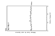
- the etching stopper film 2 has a maximum peak of the N1s narrow spectrum obtained by analysis by X-ray photoelectron spectroscopy (XPS) below the detection lower limit. If the N1s narrow spectrum peak exists, Cr—N bonds exist in the chromium-based material forming the etching stopper film 2 in a predetermined ratio or more. If Cr—N bonds are present in a predetermined ratio or more in the material forming the etching stopper film 2, it becomes difficult to suppress the progress of side etching when the etching stopper film 2 is patterned by dry etching under a high bias condition. . In the present invention, it is desirable that the nitrogen (N) content in the etching stopper film 2 is not more than a detection limit value.
- XPS X-ray photoelectron spectroscopy
- the etching stopper film 2 has a maximum peak at a binding energy of 574 eV or less in the narrow spectrum of Cr2p obtained by analysis by X-ray photoelectron spectroscopy.
- a chromium-based material when the narrow spectrum of Cr2p has a maximum peak with a binding energy higher than 574 eV, that is, in a state of chemical shift, chromium bonded to other atoms (particularly nitrogen) It shows that the atomic ratio is high. Since such a chromium-based material tends to have low resistance to dry etching due to a chemical reaction that contributes to etching in the side wall direction of the pattern, it is difficult to suppress the progress of side etching.
- the etching stopper film 2 is formed of a chromium-based material in which the narrow spectrum of Cr2p obtained by analysis by X-ray photoelectron spectroscopy has a maximum peak at a binding energy of 574 eV or less. In this case, it is possible to suppress the progress of side etching when patterning such an etching stopper film 2 by dry etching under a high bias condition.
- the ratio Cc / Ct obtained by dividing the carbon content Cc [atomic%] in the etching stopper film 2 by the total content Ct [atomic%] of chromium, carbon, and oxygen is 0.1 or more. Preferably, it is 0.14 or more.
- the etching stopper film 2 is made of a material containing chromium, oxygen and carbon, and the chromium in the etching stopper film 2 is in the form of Cr—O bond, Cr—C bond, oxygen and carbon. Many exist in any form that is not coupled to any of them.
- a chromium-based material having a high ratio Cc / Ct obtained by dividing the carbon content Cc [atomic%] by the total content Ct [atomic%] of chromium, carbon, and oxygen is the presence of a Cr—C bond in the material.
- the ratio is high, and the progress of side etching when such a chromium-based material is patterned by dry etching under a high bias condition can be suppressed.
- the etching stopper film 2 is made of a material containing chromium, oxygen and carbon, and the total content of these chromium, oxygen and carbon is preferably 95 atomic% or more, more preferably 98 atomic%. That's it.
- the etching stopper film 2 is particularly preferably composed of the above chromium, oxygen and carbon except for impurities which are unavoidably mixed during film formation.
- the impurities inevitably mixed here are elements such as argon, helium, neon, krypton, xenon and hydrogen contained in the sputtering gas when the etching stopper film 2 is formed by sputtering.
- the etching stopper film 2 preferably has an oxygen content of 10 atomic% to 35 atomic%.
- oxygen in such a range in the chromium-based material forming the etching stopper film 2, the etching rate in the case of dry etching under a high bias condition is significantly increased, and the etching time in the film thickness direction is increased. Can be greatly shortened.
- the etching stopper film 2 preferably has a carbon content of 10 atomic% to 20 atomic%. Inclusion of carbon in such a range in the chromium-based material forming the etching stopper film 2 increases the etching rate in the case of dry etching under high bias conditions and suppresses the progress of side etching. Can do.
- the maximum peak of the Si2p narrow spectrum obtained by analysis by X-ray photoelectron spectroscopy is not more than the detection lower limit value.
- the peak of the narrow spectrum of Si2p exists, unbonded silicon and silicon bonded to other atoms are present in a predetermined ratio or more in the material forming the etching stopper film 2.
- the etching stopper film 2 preferably has a silicon content of 1 atomic% or less, and more preferably a detection limit value or less.
- the method for forming the etching stopper film 2 is not particularly limited, but a sputtering film forming method is particularly preferable.
- the sputtering film forming method is preferable because a uniform film having a constant film thickness can be formed. Since the etching stopper film 2 is formed using a highly conductive target, it is more preferable to use DC sputtering with a relatively high deposition rate.
- the thickness of the etching stopper film 2 is not particularly limited, but is preferably in the range of, for example, 3 nm to 20 nm, and more preferably 3.5 nm to 15 nm.
- the light shielding film 3 is made of a material containing one or more elements selected from silicon and tantalum.
- the etching stopper film 2 made of the above-mentioned chromium-based material.
- Examples of a material containing one or more elements selected from silicon and tantalum that form the light-shielding film 3 include the following materials in the present invention.
- Examples of the material containing silicon include a material composed of silicon and nitrogen, or a material containing one or more elements selected from metalloid elements and nonmetallic elements in this material.
- the metalloid element in this case is preferably one or more elements selected from boron, germanium, antimony and tellurium.
- the nonmetallic element includes a nonmetallic element in a narrow sense (nitrogen, carbon, oxygen, phosphorus, sulfur, selenium), a halogen, and a noble gas.
- materials containing silicon suitable for the light-shielding film 3 materials containing one or more elements selected from oxygen, nitrogen, carbon, boron and hydrogen in silicon and transition metals can be cited.
- the transition metal in this case include molybdenum (Mo), tungsten (W), titanium (Ti), tantalum (Ta), zirconium (Zr), hafnium (Hf), niobium (Nb), vanadium (V), Examples include cobalt (Co), nickel (Ni), ruthenium (Ru), tin (Sn), and chromium (Cr).
- Such a material containing silicon and a transition metal has high light shielding performance, and the thickness of the light shielding film 3 can be reduced.
- the material containing tantalum in addition to tantalum metal, a material containing one or more elements selected from nitrogen, oxygen, boron and carbon in tantalum is used.
- a material containing one or more elements selected from nitrogen, oxygen, boron and carbon in tantalum is used.
- Ta, TaN, TaO, TaON, TaBN, TaBO, TaBON, TaCN, TaCO, TaCON, TaBCN, TaBOCN and the like are preferable.
- the method for forming the light shielding film 3 is not particularly limited, and among these, a sputtering film forming method is preferable.
- the sputtering film forming method is preferable because a uniform film having a constant film thickness can be formed.
- the light-shielding film 3 is formed of a material composed of silicon and nitrogen, or a material containing one or more elements selected from a semi-metal element and a non-metal element in this material, the conductivity of the target is low, so that RF (Radio) (Frequency) sputtering or ion beam sputtering is preferable.
- the light-shielding film 3 is formed of a material containing one or more elements selected from oxygen, nitrogen, carbon, boron and hydrogen or a material containing tantalum on silicon and a transition metal, the conductivity of the target is high. Since it is relatively high, it is preferable to form a film using DC sputtering, which has a relatively high film formation speed.
- the light shielding film 3 may have a single layer structure or a laminated structure.
- a two-layer structure of a light-shielding layer and a front-surface antireflection layer, or a three-layer structure further including a back-surface antireflection layer can be used.
- the light-shielding film 3 is required to ensure a predetermined light-shielding property.
- the optical density (OD) with respect to exposure light of an ArF excimer laser (wavelength 193 nm) effective for forming a fine pattern is 2.8 or more. It is calculated
- the thickness of the light-shielding film 3 is not particularly limited, but is preferably 80 nm or less and more preferably 70 nm or less so that a fine pattern can be accurately formed in the binary mask blank.
- the thickness of the light shielding film 3 is preferably 30 nm or more, and preferably 40 nm or more. Is more preferable.
- a hard mask film made of a material having an etching selectivity with respect to the light shielding film 3 is formed on the light shielding film 3.
- (It may be called an “etching mask film”.) 4 is preferably provided.
- the material of the hard mask film 4 functions as an etching mask when a pattern is formed on the light shielding film 3 by dry etching, the material of the hard mask film 4 has sufficient resistance to the dry etching environment of the light shielding film 3. It is necessary to form with material.
- a fluorine-based gas is usually used as an etching gas.
- the material of the hard mask film 4 it is preferable to use a chromium-based material containing chromium having sufficient etching selectivity with the light-shielding film 3 with respect to the dry etching of the fluorine-based gas. .
- the chromium-based material forming the hard mask film 4 examples include a chromium compound obtained by adding one or more elements selected from elements such as oxygen, carbon, nitrogen, hydrogen, and boron to chromium.
- the hard mask film 4 is patterned by dry etching using a mixed gas of chlorine gas and oxygen gas using the pattern of the resist film formed on the surface of the mask blank 10 as a mask. It is preferable that the etching rate in dry etching with a mixed gas with oxygen gas is fast.
- the hard mask film 4 is preferably made of a material containing at least chromium and oxygen.
- the hard mask film 4 is more preferably a single layer film using the same material as the etching stopper film 2. In this case, the surface of the hard mask film 4 on the side opposite to the translucent substrate 1 side and the region in the vicinity thereof are difficult to avoid the progress of oxidation, so that the single layer film having a composition gradient portion with an increased oxygen content and become.
- the method for forming the hard mask film 4 is not particularly limited, but a sputtering film forming method is particularly preferable.
- the sputtering film forming method is preferable because a uniform film having a constant film thickness can be formed. Since the hard mask film 4 is formed using a highly conductive target, it is more preferable to use DC sputtering with a relatively high deposition rate.
- the thickness of the hard mask film 4 is not particularly limited, the hard mask film 4 functions as an etching mask when patterning the light shielding film 3 immediately below by dry etching using a fluorine-based gas. At least a film thickness that does not disappear before the etching of the light shielding film 3 directly below is required. On the other hand, if the hard mask film 4 is too thick, it is difficult to reduce the thickness of the resist film pattern directly above. From such a viewpoint, the film thickness of the hard mask film 4 is preferably in the range of 3 nm to 15 nm, for example, and more preferably 3.5 nm to 10 nm.
- the mask blank of the present invention includes a form having a resist film on the surface of the mask blank 10 having the above configuration.
- the resist film is made of an organic material and is preferably a resist material for electron beam drawing, and a chemically amplified resist material is particularly preferably used.
- the resist film is usually formed on the surface of the mask blank by a coating method such as spin coating.
- the resist film preferably has a thickness of, for example, 200 nm or less from the viewpoint of fine pattern formation. However, by providing the hard mask film 4, the resist film can be made thinner, for example, 100 nm or less. It can be a film thickness.
- the light-shielding layer made of the chromium-based material having the configuration of the present invention, the silicon-based material, or the tantalum-based material is formed on the translucent substrate 1.
- the mask blank of the present invention is particularly suitable when it is required to form a fine pattern (for example, a SRAF (Sub Resolution Assist Features) pattern having a dimension of 50 nm or less) with high pattern accuracy.
- a fine pattern for example, a SRAF (Sub Resolution Assist Features) pattern having a dimension of 50 nm or less
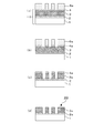
- FIG. 3 is a schematic cross-sectional view showing a manufacturing process of a transfer mask using the mask blank of the first embodiment described above.
- a resist film for electron beam drawing is formed on the surface of the mask blank 10 with a predetermined film thickness by, eg, spin coating.
- a predetermined pattern is drawn on the resist film with an electron beam, developed, and then developed to form a predetermined resist film pattern 6a (see FIG. 3A).
- the resist film pattern 6a has a desired device pattern to be formed on the light-shielding film 3 to be a final transfer pattern.
- a hard mask film pattern 4a is formed on the hard mask film 4 made of a chromium-based material by dry etching using a mixed gas of chlorine-based gas and oxygen gas (FIG. 3 (b)).
- the light shielding film 3 made of a silicon-based material or a tantalum-based material is shielded by dry etching using a fluorine-based gas using the hard mask film pattern 4a as a mask.
- a film pattern 3a is formed (see FIG. 3C).
- the hard mask film pattern 4a is removed by dry etching using a mixed gas of chlorine gas and oxygen gas, and the light shielding film pattern 3a is used as a mask to form the chromium material of the structure of the present invention.
- a pattern 2a is formed on the etching stopper film 2 (see FIG. 3D). In the present invention, in this case, it is preferable to apply the dry etching under the high bias condition described above.
- the mask blank 10 of this embodiment By using the mask blank 10 of this embodiment, side etching that occurs on the pattern side wall of the etching stopper film 2 when the etching stopper film 2 is patterned by dry etching using a mixed gas of chlorine-based gas and oxygen gas is performed. Can be suppressed. As a result, the transfer pattern (the light shielding film pattern 3a) can be prevented from being tilted due to the narrowing of the pattern 2a of the etching stopper film 2, and a fine transfer pattern can be formed with high accuracy.
- the binary transfer mask 20 having the fine light-shielding film pattern 3a to be a transfer pattern on the translucent substrate 1 is completed (see FIG. 3D).
- the transfer mask 20 on which a highly accurate fine transfer pattern is formed can be manufactured.
- the method includes the step of exposing and transferring the transfer pattern of the transfer mask to a resist film on the semiconductor substrate by lithography using the transfer mask 20 manufactured using the mask blank of the present embodiment. According to the semiconductor device manufacturing method, it is possible to manufacture a high-quality semiconductor device in which a device pattern with excellent pattern accuracy is formed.
- the present invention is applied to a binary mask blank, and a binary transfer mask manufactured using the binary mask blank of this embodiment has been described.
- the mask blank of the above-described embodiment is described. It is also possible to manufacture, for example, a substrate digging type phase shift mask (for example, a digging Levenson type phase shift mask, a chromeless phase shift mask, etc.) using a mask blank having the same configuration as in FIG. That is, the mask blank of this embodiment can also be used as a mask blank for producing the phase shift mask.
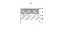
- FIG. 2 is a schematic cross-sectional view showing a second embodiment of a mask blank according to the present invention.
- the mask blank 30 according to the second embodiment of the present invention is a light-shielding film made of a phase shift film 5, an etching stopper film 2, a silicon-based material or a tantalum-based material on a translucent substrate 1.
- This is a phase shift mask blank having a structure in which a film 3 and a hard mask film 4 made of a chromium-based material are stacked in this order.
- the etching stopper film 2 has the configuration of the present invention. That is, the etching stopper film 2 of the present embodiment is made of a material containing chromium, oxygen and carbon, and the chromium content is 50 atomic% or more. Further, the etching stopper film 2 is formed by X-ray photoelectron spectroscopy. The maximum peak of the N1s narrow spectrum obtained by analyzing with the above is below the detection lower limit value, and the narrow spectrum of Cr2p obtained by analyzing by X-ray photoelectron spectroscopy has the maximum peak with a binding energy of 574 eV or less It is. The details of the etching stopper film 2 of the present embodiment are the same as those in the case of the etching stopper film of the first embodiment described above.
- the details of the translucent substrate 1, the light shielding film 3, and the hard mask film 4 in the mask blank 30 of the present embodiment are the same as in the case of the first embodiment described above. Duplicate explanation is omitted.
- the sputtering film forming method is suitable as in the case of the first embodiment. It is. The film thicknesses of these films are the same as in the case of the first embodiment.
- the laminated structure of the phase shift film 5, the etching stopper film 2, and the light shielding film 3 is used.
- the optical density (OD) with respect to exposure light of an ArF excimer laser (wavelength 193 nm) is required to be 2.8 or more, and more preferably 3.0 or more.
- the phase shift film 5 is formed of a material containing silicon.
- the configuration of the phase shift film 5 applied to the present embodiment is not particularly limited, and has been used, for example, so far.
- the structure of the phase shift film in the phase shift mask can be applied.
- the phase shift film 5 includes, for example, a material containing silicon, a material containing a transition metal and silicon, optical properties (light transmittance, phase difference, etc.), physical properties (etching rate, other films (layers) of the film. In order to improve the etching selectivity between and the like, it is further formed of a material containing at least one element of nitrogen, oxygen and carbon.
- the silicon-containing material examples include silicon nitride, oxide, carbide, oxynitride (oxynitride), carbonate (carbide oxide), and carbonitride (carbonitride oxynitride). ) Is preferred.
- a transition metal silicide composed of a transition metal and silicon, or a transition metal silicide nitride, oxide, carbide, oxynitride, carbonate, or A material containing carbonitride is preferred.
- molybdenum As the transition metal, molybdenum, tantalum, tungsten, titanium, chromium, hafnium, nickel, vanadium, zirconium, ruthenium, rhodium, niobium, and the like are applicable. Of these, molybdenum is particularly preferred.
- the phase shift film 5 can be applied to either a single layer structure or a laminated structure including a low transmittance layer and a high transmittance layer.
- the preferable film thickness of the phase shift film 5 varies depending on the material, but it is desirable to adjust as appropriate from the viewpoint of the phase shift function and light transmittance.
- the thickness of the phase shift film 5 is usually in the range of, for example, 100 nm or less, more preferably 80 nm or less.
- a method for forming the phase shift film 5 is not particularly limited, but a sputtering film forming method is preferable.
- the mask blank of the present invention includes a form having a resist film on the surface of the mask blank 30 having the above-described configuration.
- this resist film it is the same as that of the case of the above-mentioned 1st Embodiment.
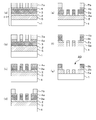
- FIG. 4 is a schematic cross-sectional view showing a manufacturing process of a transfer mask (halftone phase shift mask) using the mask blank 30 of the second embodiment described above.
- a resist film for electron beam drawing is formed on the surface of the mask blank 30 with a predetermined film thickness, for example, by spin coating.
- a predetermined pattern is drawn on the resist film with an electron beam, and after the drawing, development is performed to form a predetermined resist film pattern 7a (see FIG. 4A).
- the resist film pattern 7a has a desired device pattern to be formed on the phase shift film 5 to be a final transfer pattern.
- a hard mask film pattern 4a is formed on the hard mask film 4 made of a chromium-based material by dry etching using a mixed gas of chlorine-based gas and oxygen gas (FIG. 4 (b)).
- the light shielding film 3 made of a silicon-based material or a tantalum-based material is shielded by dry etching using a fluorine-based gas using the hard mask film pattern 4a as a mask.
- a film pattern 3a is formed (see FIG. 4C).
- a resist film similar to the above is formed on the entire surface of the mask blank on which the light shielding film pattern 3a is formed, and a predetermined light shielding pattern (for example, a light shielding band pattern) is drawn on the resist film. Thereafter, development is performed to form a resist film pattern 7b having a predetermined light-shielding pattern on the hard mask film 4 (hard mask film pattern 4a) (see FIG. 4D).
- a predetermined light shielding pattern for example, a light shielding band pattern
- an etching stopper film 2 made of a chromium-based material of the present invention is formed by dry etching using a mixed gas of chlorine-based gas and oxygen gas, using the light-shielding film pattern 3a formed on the light-shielding film 3 as a mask.
- a pattern 2a is formed on the hard mask film 4 using the resist pattern 7b as a mask (see FIG. 4E).
- the phase shift film pattern 5a is formed on the phase shift film 5 by using the pattern 2a formed on the etching stopper film 2 as a mask by dry etching using a fluorine-based gas.
- the hard mask film pattern 4b as a mask, a part of the light shielding film light shielding pattern 3a is removed to form a light shielding film pattern 3b (see FIG. 4F).
- a pattern having a light shielding pattern on the etching stopper film 2 (pattern 2a) using the light shielding film pattern 3b on which the light shielding pattern is formed by dry etching using a mixed gas of chlorine gas and oxygen gas as a mask. 2b is formed and the remaining hard mask film pattern 4b is removed (see FIG. 4G).
- the halftone phase shift mask (transfer mask) 40 including the fine pattern 5a of the phase shift film serving as a transfer pattern and the light-shielding pattern (light-shielding band pattern) in the outer peripheral region on the translucent substrate 1. Is completed (see FIG. 4G).
- the light shielding film pattern 3a formed on the light shielding film 3 is used as a mask, and the etching stopper film 2 is subjected to dry etching using a mixed gas of chlorine gas and oxygen gas. Side etching that occurs on the pattern sidewall of the etching stopper film 2 during patterning (step of FIG. 4E) can be suppressed. As a result, the light shielding film pattern 3a can be prevented from falling due to the narrowing of the pattern 2a of the etching stopper film 2, and even a fine pattern can be formed with high accuracy. Further, by patterning the phase shift film 5 using the pattern 2a of the etching stopper film 2 as a mask (step (f) in FIG. 4), it is possible to form a fine transfer pattern on the phase shift film 5 with high accuracy. Become.
- a transfer mask (halftone phase shift mask) 40 on which a highly accurate fine transfer pattern is formed can be manufactured.
- a semiconductor device including a step of exposing and transferring a transfer pattern of the transfer mask onto a resist film on a semiconductor substrate by lithography using the transfer mask 40 manufactured from the mask blank 30 of the present embodiment. According to this manufacturing method, it is possible to manufacture a high-quality semiconductor device on which a device pattern with excellent pattern accuracy is formed.
- Example 1 relates to manufacture of a mask blank and a transfer mask used for manufacturing a transfer mask (binary mask) using an ArF excimer laser having a wavelength of 193 nm as exposure light, and corresponds to the first embodiment described above.
- the mask blank 10 used in Example 1 has a structure in which an etching stopper film 2, a light shielding film 3, and a hard mask film 4 are laminated in this order on a light transmitting substrate 1 as shown in FIG.
- This mask blank 10 was produced as follows.
- a translucent substrate 1 (size: about 152 mm ⁇ 152 mm ⁇ thickness: about 6.35 mm) made of synthetic quartz glass was prepared.
- the translucent substrate 1 has its main surface and end surfaces polished to a predetermined surface roughness (for example, the main surface has a root mean square roughness Rq of 0.2 nm or less).
- the translucent substrate 1 is installed in a single wafer DC sputtering apparatus, and a target made of chromium is used in a mixed gas atmosphere of argon (Ar), carbon dioxide (CO 2 ), and helium (He).
- argon Ar
- CO 2 carbon dioxide
- He helium
- an etching stopper film 2 made of a CrOC film containing chromium, oxygen and carbon was formed to a thickness of 10 nm on the main surface of the translucent substrate 1.
- a lower layer of a light shielding film made of (Mo: 9.2 atomic%, Si: 68.3 atomic%, N: 22.5 atomic%) was formed to a thickness of 47 nm.
- a MoSiN film containing molybdenum, silicon and nitrogen is formed on the lower layer of the light shielding film by DC sputtering using a mixed gas of nitrogen (N 2 ) and argon (Ar).
- the upper layer of the light-shielding film made of Mo: 5.8 atomic%, Si: 64.4 atomic%, and N: 27.7 atomic% was formed to a thickness of 4 nm.
- a MoSi-based light shielding film 3 having a two-layer structure with a total thickness of 51 nm was formed.
- the optical density of the laminated film of the formed MoSi-based light shielding film 3 was 3.0 or more at the wavelength of ArF excimer laser (193 nm).
- the translucent substrate 1 on which the etching stopper film 2 and the light-shielding film 3 are formed is placed in a single wafer DC sputtering apparatus, and a target made of chromium is used to make argon (Ar) and carbon dioxide (CO 2 ). ) And helium (He) mixed gas under the same film forming conditions as those for forming the etching stopper film 2, so that the surface of the light shielding film 3 contains CrOC containing chromium, oxygen and carbon.
- a hard mask film 4 made of a film was formed with a thickness of 10 nm.
- the mask blank 10 of Example 1 was produced as described above.
- a material in which only the etching stopper film 2 was formed on the main surface of another translucent substrate under the same conditions as described above was prepared.
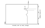
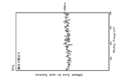
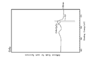
- the etching stopper film 2 was analyzed by X-ray photoelectron spectroscopy (with RBS (Rutherford Backscattering Spectrometry) correction). As a result, it was confirmed that the content of each constituent element in the etching stopper film 2 was an average value of Cr: 71 atomic%, O: 15 atomic%, and C: 14 atomic%. Further, the difference in the content of each constituent element in the thickness direction of the etching stopper film 2 is 3 atomic% or less (however, the region near the surface of the etching stopper film 2 whose analysis results are affected by the atmosphere is excluded.
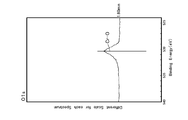
- FIG. 6 shows the results of the chemical direction analysis of the O1s narrow spectrum in the depth direction
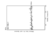
- FIG. 7 shows the results of the chemical direction analysis of the N1s narrow spectrum in the depth direction
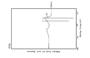
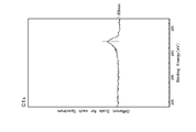
- FIG. 8 shows the depth direction of the C1s narrow spectrum.
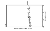
- the result of chemical bonding state analysis is shown in FIG. 9, and the result of chemical bonding state analysis in the depth direction of the Si2p narrow spectrum is shown in FIG.
- X-rays are irradiated toward the surface of the etching stopper film 2 to measure the energy distribution of photoelectrons emitted from the etching stopper film 2, and then Ar gas.
- Example 1 the analysis by the X-ray photoelectron spectroscopy uses monochromatic Al (1486.6 eV) as the X-ray source, the photoelectron detection region is 100 ⁇ m ⁇ , and the detection depth is about 4 to 5 nm ( The extraction angle was 45 degrees) (the same applies to the following examples and comparative examples).
- the position in the film thickness direction of the etching stopper film 2 after being dug by Ar gas sputtering from the outermost surface of the etching stopper film 2 by 1.60 min is a position having a depth of about 6 nm from the surface.
- the plot of “60 min” is the measurement result at the position of the depth.
- the scale of the vertical axis in each narrow spectrum of FIGS. 6 to 10 is not the same.
- the N1s narrow spectrum in FIG. 8 and the Si2p narrow spectrum in FIG. 10 are greatly expanded in scale on the vertical axis as compared with the narrow spectra in FIG. 6, FIG. 7 and FIG. Therefore, the vibration wave in the N1s narrow spectrum of FIG. 8 and the Si2p narrow spectrum of FIG. 10 does not show the presence of a peak but only shows noise.
- the etching stopper film 2 of Example 1 has a maximum peak at a binding energy of 574 eV. This result means that in the etching stopper film 2, atoms such as oxygen and unbonded chromium atoms are present in a certain ratio or more.
- Example 7 shows that the etching stopper film 2 of Example 1 has a maximum peak at a binding energy of about 530 eV from the result of the O1s narrow spectrum in FIG. This result means that the etching stopper film 2 has a Cr—O bond of a certain ratio or more.
- the etching stopper film 2 of Example 1 has the maximum peak at a binding energy of 282 eV to 283 eV. This result means that in the etching stopper film 2, Cr—C bonds exist in a certain ratio or more.
- a transfer mask (binary mask) was manufactured using the mask blank 10 according to the manufacturing process shown in FIG.
- the following symbols correspond to the symbols in FIG.
- a chemical amplification resist for electron beam drawing PRL009 manufactured by Fuji Film Electronics Materials Co., Ltd.
- PRL009 manufactured by Fuji Film Electronics Materials Co., Ltd.
- a predetermined baking process is performed, so that the film thickness is 80 nm.
- a resist film was formed.
- the resist film is developed to form a resist film pattern. 6a was formed (see FIG. 3A).
- the resist film pattern 6a includes an SRAF pattern having a line width of 50 nm.
- the hard mask film 4 was dry-etched by dry etching under the above-described high bias condition to form a hard mask film pattern 4a (see FIG. 3B).
- the MoSi-based light shielding film 3 having a two-layer structure is continuously subjected to dry etching to form the light shielding film pattern 3a ( (Refer FIG.3 (c)).
- a fluorine-based gas SF 6
- SF 6 fluorine-based gas
- the etching stopper film 2 is etched using the light shielding film pattern 3a as a mask to form a pattern 2a on the etching stopper film 2, and the hard mask film pattern 4a is It removed (refer FIG.3 (d)).
- the transfer mask 20 of Example 1 is separately manufactured, a cross-sectional STEM (Scanning Transmission Electron Microscope) image of the region where the SRAF pattern is formed is obtained, and the light shielding film pattern 3a and the etching stopper film are obtained. The line width of each pattern 2a was measured.
- the etching bias which is the amount of change between the line width of the light shielding film pattern 3a and the line width of the pattern 2a of the etching stopper film.
- the etching bias was about 6 nm, which was much smaller than that in the case of dry etching for a conventional chromium-based material film.
- the pattern of the etching stopper film 2 is used even when the etching stopper film 2 is patterned by dry etching under a high bias condition using the light shielding film pattern 3a as a mask and using a mixed gas of chlorine gas and oxygen gas. It shows that side etching occurring on the side wall can be suppressed. In addition, this makes it possible to suppress the tilting of the light-shielding film pattern 3a due to the thinning of the pattern 2a of the etching stopper film 2. For example, even a transfer pattern having a fine pattern such as an SRAF pattern with a line width of 50 nm or less is accurate. It shows that it can be formed well.
- the transfer mask 20 on which a highly accurate fine transfer pattern is formed can be manufactured.
- an exposure transfer image was simulated when the transfer mask 20 was exposed and transferred to a resist film on a semiconductor device with exposure light having a wavelength of 193 nm using AIMS 193 (manufactured by Carl Zeiss).
- AIMS 193 manufactured by Carl Zeiss
- the design specifications were sufficiently satisfied. From the above, when the transfer mask 20 manufactured from the mask blank of Example 1 is set in an exposure apparatus and subjected to exposure transfer with exposure light of an ArF excimer laser, it is applied to the resist film on the semiconductor device. It can be said that exposure transfer can be performed with high accuracy.
- Example 2 The mask blank 10 of Example 2 was produced in the same manner as Example 1 except for the etching stopper film 2.
- the etching stopper film 2 in Example 2 was formed by changing the film forming conditions as compared with the etching stopper film 2 of Example 1 as follows.
- the same translucent substrate 1 as in Example 1 is installed, and a target made of chromium is used, and argon (Ar), carbon dioxide (CO 2 ), and helium ( By performing reactive sputtering in a mixed gas atmosphere of He), an etching stopper film 2 made of a CrOC film containing chromium, oxygen, and carbon is formed on the main surface of the translucent substrate 1 with a thickness of 10 nm. Formed. Next, a MoSi light-shielding film 3 was formed on the etching stopper film 2 under the same conditions as in Example 1.
- the translucent substrate 1 on which the etching stopper film 2 and the light-shielding film 3 are formed is placed in a single wafer DC sputtering apparatus, and a target made of chromium is used to make argon (Ar) and carbon dioxide (CO 2 ). ) And helium (He) mixed gas is sputtered under the same film forming conditions as those for forming the etching stopper film 2 of Example 2, so that chromium, oxygen and carbon are formed on the surface of the light shielding film 3.
- a hard mask film 4 made of a CrOC film containing bismuth was formed with a thickness of 10 nm.
- the mask blank 10 of Example 2 was produced as described above.
- etching stopper film 2 of Example 2 was analyzed by X-ray photoelectron spectroscopy (with RBS correction). As a result, it was confirmed that the content of each constituent element in the etching stopper film 2 was, on average, Cr: 55 atomic%, O: 30 atomic%, and C: 15 atomic%. Further, the difference in the content of each constituent element in the thickness direction of the etching stopper film 2 is 3 atomic% or less (however, the region near the surface of the etching stopper film 2 whose analysis results are affected by the atmosphere is excluded.
- FIG. 11 shows the results of the chemical direction analysis of the depth direction of FIG. 11
- FIG. 12 shows the results of the chemical state analysis of the depth direction of the O1s narrow spectrum
- FIG. 13 shows the results of the chemical direction analysis of the N1s narrow spectrum
- FIG. 14 shows the results of the chemical direction analysis in the depth direction of the C1s narrow spectrum
- FIG. 15 shows the results of the chemical direction analysis in the depth direction of the Si2p narrow spectrum.
- the scale of the vertical axis in each narrow spectrum in FIGS. 11 to 15 is not the same.
- the N1s narrow spectrum of FIG. 13 and the Si2p narrow spectrum of FIG. 15 are greatly expanded in scale on the vertical axis as compared with the narrow spectra of FIGS. Therefore, the vibration wave in the N1s narrow spectrum of FIG. 13 and the Si2p narrow spectrum of FIG. 15 does not show the presence of a peak but only shows noise.
- the etching stopper film 2 of Example 2 has a maximum peak at a binding energy of 574 eV. This result means that in the etching stopper film 2, atoms such as oxygen and unbonded chromium atoms are present in a certain ratio or more.
- the etching stopper film 2 of Example 2 has a maximum peak at a binding energy of about 530 eV. This result means that the etching stopper film 2 has a Cr—O bond of a certain ratio or more.
- the etching stopper film 2 of Example 2 has a maximum peak at a binding energy of 282 eV to 283 eV from the result of the C1s narrow spectrum in FIG. This result means that in the etching stopper film 2, Cr—C bonds exist in a certain ratio or more.
- the pattern 2a of the etching stopper film 2 and the light-shielding film pattern 3a are laminated on the translucent substrate 1 according to the same manufacturing process as in Example 1 described above.
- a transfer mask (binary mask) 20 having a transfer pattern was manufactured.
- the transfer mask 20 of the second embodiment is manufactured separately in the same procedure as the first embodiment, a cross-sectional STEM image of the region where the SRAF pattern is formed is obtained, and the pattern of the light shielding film pattern 3a and the etching stopper film 2 is obtained. Each line width of 2a was measured.
- the etching bias is about 10 nm. The value was much smaller than in the case of dry etching on the film.
- Example 2 exposure was performed when the transfer mask 20 of Example 2 was exposed and transferred to the resist film on the semiconductor device with exposure light having a wavelength of 193 nm using AIMS 193 (manufactured by Carl Zeiss) as in Example 1.
- the transfer image was simulated. When the exposure transfer image obtained by this simulation was verified, the design specifications were sufficiently satisfied. From the above, when the transfer mask 20 manufactured from the mask blank of Example 2 is set in an exposure apparatus and subjected to exposure transfer with exposure light of an ArF excimer laser, the transfer mask 20 is higher than the resist film on the semiconductor device. It can be said that exposure transfer can be performed with high accuracy.
- Example 3 relates to manufacture of a mask blank and a halftone phase shift mask (transfer mask) used for manufacturing a halftone phase shift mask (transfer mask) using an ArF excimer laser with a wavelength of 193 nm as exposure light.
- a mask blank 30 used in Example 3 is formed by laminating a phase shift film 5, an etching stopper film 2, a light shielding film 3, and a hard mask film 4 in this order on a light transmitting substrate 1 as shown in FIG. Of structure.
- This mask blank 30 was produced as follows.
- a MoSiN film (Mo: 4.1 atomic%, Si: 35.6 atomic%, N: 60.3) containing molybdenum, silicon, and nitrogen is formed on the surface of the translucent substrate 1 by sputtering using a sputtering gas.
- a phase shift film 5 composed of 69% of atomic percent was formed.
- the translucent substrate 1 on which the phase shift film 5 was formed was taken out of the sputtering apparatus, and the phase shift film 5 on the translucent substrate was subjected to a heat treatment in the atmosphere.
- This heat treatment was performed at 450 ° C. for 30 minutes.
- the transmittance is 6.44% and the phase The shift amount was 174.3 degrees.
- the translucent substrate on which the phase shift film 5 is formed is again introduced into the sputtering apparatus, and the CrOC film of Example 1 is formed on the phase shift film 5 under the same film formation conditions as in Example 1.
- the mask blank 30 of Example 3 was produced as described above.
- a halftone phase shift mask was manufactured using the mask blank 30 according to the manufacturing process shown in FIG.
- the following symbols correspond to the symbols in FIG.
- a chemical amplification resist for electron beam drawing PRL009 manufactured by Fuji Film Electronics Materials Co., Ltd.
- PRL009 manufactured by Fuji Film Electronics Materials Co., Ltd.
- a predetermined baking process is performed, so that the film thickness is 80 nm.
- a resist film was formed.
- the resist film is developed to form a resist film A pattern 7a was formed (see FIG. 4A).
- the resist film pattern 7a includes a SRAF pattern having a line width (50 nm).
- the hard mask film 4 was dry-etched by dry etching under the above-described high bias condition to form a hard mask film pattern 4a (see FIG. 4B).
- etching of the MoSi-based light shielding film 3 is continuously performed by dry etching using a fluorine-based gas using the hard mask film pattern 4a as a mask.
- a light shielding film pattern 3a was formed (see FIG. 4C).
- a fluorine-based gas SF 6
- SF 6 fluorine-based gas
- a resist film similar to the above is formed on the entire surface of the mask blank on which the light shielding film pattern 3a is formed, and a predetermined light shielding pattern (light shielding band pattern) is drawn on the resist film.
- a resist film pattern 7b having a predetermined light shielding pattern was formed on the hard mask film 4 (hard mask film pattern 4a) (see FIG. 4D).
- the pattern 2a is formed on the etching stopper film 2 made of a chromium material having the structure of the present invention using the light shielding film pattern 3a as a mask.
- a pattern 4b having the light shielding pattern was formed on the hard mask film 4 (see FIG. 4E).
- the phase shift film pattern 5a is formed on the phase shift film 5 by dry etching using a fluorine-based gas using the pattern 2a formed on the etching stopper film 2 as a mask.
- a fluorine-based gas SF 6
- SF 6 fluorine-based gas
- the light shielding in which the light shielding pattern is formed by dry etching using a mixed gas (Cl 2 : O 2 4: 1 (flow rate ratio)) of chlorine gas (Cl 2 ) and oxygen gas (O 2 ).
- chlorine gas Cl 2
- oxygen gas O 2
- the halftone phase shift mask (transfer mask) 40 having the phase shift film pattern 5a as a transfer pattern and the light shielding pattern (light shielding band pattern) in the outer peripheral region on the translucent substrate 1 is completed. (See FIG. 4 (g)). As a result of inspecting the obtained phase shift mask 40 with a mask inspection apparatus using a mask inspection apparatus, it was confirmed that the fine pattern of the phase shift film was formed within the allowable range from the design value.
- the light shielding film pattern 3a formed on the light shielding film 3 is used as a mask, and the etching stopper film 2 is dry-etched using a mixed gas of chlorine-based gas and oxygen gas. Since side etching occurring on the pattern side wall of the etching stopper film 2 during patterning (step of FIG. 4E) can be suppressed, and the fall of the light shielding film pattern 3a due to the narrowing of the pattern 2a of the etching stopper film 2 can be suppressed. Even a fine light-shielding film pattern (transfer pattern) can be formed with high accuracy.
- phase shift film 5 is formed using the pattern 2a of the etching stopper film 2 without a narrow pattern width by side etching as a mask (step of FIG. 4 (f)).
- a fine transfer pattern is also formed on the phase shift film 5. Can be formed with high accuracy.
- phase shift mask 40 manufactured from the mask blank of Example 3 can perform exposure transfer on the resist film on the semiconductor device with high accuracy.
- Example 4 relates to the manufacture of a substrate digging type phase shift mask (chromeless phase shift mask) using a mask blank having the same configuration as the mask blank 10 of Example 1, and the manufacturing process shown in FIG. It explains according to.
- the mask blank used in Example 4 has a structure in which an etching stopper film 2, a light-shielding film 3, and a hard mask film 4 are laminated in this order on a translucent substrate 1, and was produced as follows. .
- a translucent substrate 1 (synthetic quartz substrate) prepared in the same manner as in Example 1 was placed in a single-wafer DC sputtering apparatus, and the same film forming conditions as in Example 1 were applied on the substrate.
- An etching stopper film 2 made of a CrOC film was formed.
- a two-layered MoSi-based light-shielding film 3 of a lower layer 31 of the MoSiN film and an upper layer 32 of the MoSiN film was formed on the etching stopper film 2 under the same film formation conditions as in Example 1.
- a hard mask film 4 made of a CrOC film was formed on the light shielding film 3 under the same film forming conditions as in Example 1.
- the mask blank of Example 4 was produced as described above.
- a phase shift mask was manufactured using the mask blank of Example 4 according to the manufacturing process shown in FIG.
- a chemical amplification resist for electron beam drawing PRL009 manufactured by Fuji Film Electronics Materials Co., Ltd.
- PRL009 manufactured by Fuji Film Electronics Materials Co., Ltd.
- a predetermined baking process is performed to form a resist having a thickness of 80 nm.
- a film was formed.
- a predetermined device pattern (a pattern corresponding to a transfer pattern dug into the substrate) is drawn on the resist film using an electron beam drawing machine, and then the resist film is developed to form a resist film pattern 8a.
- the resist film pattern 8a includes a line and space pattern having a line width of 50 nm.
- the hard mask film 4 was dry-etched by dry etching under the above-described high bias condition to form a hard mask film pattern 4a (see FIG. 5B).
- dry etching of the light-shielding film 3 having a two-layer structure of MoSi is performed by using the hard mask film pattern 4a as a mask and using a fluorine-based gas (SF 6 ) as an etching gas. It performed continuously and formed the light shielding film pattern 3a (refer FIG.5 (c)).
- SF 6 fluorine-based gas
- dry etching of the etching stopper film 2 is performed by dry etching under the above-described high bias condition using the light shielding film pattern 3a as a mask to form a pattern 2a on the etching stopper film 2, and the hard mask film pattern 4a.
- a resist film similar to the above is formed on the entire surface of the mask blank on which the light shielding film pattern 3a is formed, and a predetermined light shielding pattern (light shielding band pattern) is drawn on the resist film.
- a resist film pattern 8b having a light shielding pattern was formed (see FIG. 5E).
- the exposed light shielding film pattern 3a is peeled and removed by dry etching using a fluorine-based gas, and the pattern 2a formed on the etching stopper film 2 is used as a mask.
- the light-transmitting substrate 1 synthetic quartz substrate
- the translucent substrate was dug to a depth (about 173 nm) at which a phase difference of 180 degrees was obtained.
- a mixed gas of fluorine-based gas (CF 4 ) and helium (He) was used as an etching gas for dry etching.
- the digging type phase shift pattern 1a is formed on the translucent substrate 1, and the digging type phase shift mask (transfer mask) having the light shielding pattern (light shielding band pattern) in the outer peripheral region is formed. ) 50 was completed (see FIG. 5G). As a result of inspecting the obtained phase shift mask 50 with a mask inspection apparatus using a mask inspection apparatus, it was confirmed that the phase shift pattern was formed within the allowable range from the design value.
- Example 4 when the light shielding film pattern 3a formed on the light shielding film 3 is used as a mask, the etching stopper film 2 is patterned by dry etching using a mixed gas of chlorine-based gas and oxygen gas (FIG. Side etching that occurs on the pattern side wall of the etching stopper film 2 in step (d) can be suppressed, and the fall of the light shielding film pattern 3a due to the narrowing of the pattern 2a of the etching stopper film 2 can be suppressed. Further, the substrate is dug using the pattern 2a of the etching stopper film 2 with no pattern width narrowed by side etching as a mask (step of FIG. 5 (f)), so that a fine phase shift pattern can be accurately formed by dug the substrate. can do.
- phase shift mask 50 manufactured from the mask blank of Example 4 can perform exposure transfer on the resist film on the semiconductor device with high accuracy.
- Comparative Example 1 The mask blank of Comparative Example 1 was produced in the same manner as Example 1 except for the etching stopper film.
- the etching stopper film in Comparative Example 1 was formed by changing the film formation conditions as compared with the etching stopper film 2 of Example 1 as follows. Specifically, the same translucent substrate (synthetic quartz substrate) as in Example 1 above is installed in a single wafer DC sputtering apparatus, and a target made of chromium is used, and argon (Ar) and carbon dioxide (CO 2 ).
- etching stopper film of Comparative Example 1 was analyzed by X-ray photoelectron spectroscopy (with RBS correction). As a result, the content of each constituent element in the etching stopper film of Comparative Example 1 is, on average, Cr: 55 atomic%, O: 22 atomic%, C: 12 atomic%, and N: 11 atomic%. It could be confirmed.
- the difference in the content of each constituent element in the thickness direction of the etching stopper film is 3 atomic% or less (except for the area near the surface of the etching stopper film whose analysis results are affected by the atmosphere). It was confirmed that there was substantially no composition gradient in the thickness direction.
- FIG. 16 shows the results of the chemical analysis of the chemical direction in the depth direction of the Cr2p narrow spectrum obtained as a result of the X-ray photoelectron spectroscopy analysis of the etching stopper film in Comparative Example 1.
- FIG. 17 shows the result of the chemical direction analysis of the O1s narrow spectrum in the depth direction
- FIG. 18 shows the result of the chemical direction analysis of the depth direction of the N1s narrow spectrum
- FIG. 19 shows the results of analysis of the chemical bonding state in the depth direction of the Si2p narrow spectrum, respectively.
- the etching stopper film of Comparative Example 1 has a maximum peak at a binding energy of about 530 eV. This result means that Cr—O bonds are present in a certain ratio or more.
- a transfer mask (binary mask) of Comparative Example 1 was manufactured according to the same manufacturing process as in Example 1 described above. Further, in the same procedure as in Example 1, the transfer mask of Comparative Example 1 is separately manufactured, a cross-sectional STEM image of the region where the SRAF pattern is formed is obtained, and the pattern of the light shielding film pattern and the etching stopper film is obtained. Each line width was measured.
- the etching bias is 27 nm, and dry etching with respect to a conventional chromium-based material film is performed. As in the case of, it was a relatively large value.
- etching is performed when the etching stopper film is patterned by dry etching under a high bias condition using the light shielding film pattern as a mask and using a mixed gas of chlorine gas and oxygen gas. It is difficult to suppress the side etching that occurs on the pattern sidewall of the stopper film, so that the light shielding film pattern collapses due to the narrowing of the etching stopper film pattern. For example, it is possible to accurately form a fine transfer pattern with a line width of 50 nm or less. It is difficult.
- Comparative Example 2 The mask blank of Comparative Example 2 was produced in the same manner as Example 1 except for the etching stopper film.
- the etching stopper film in Comparative Example 2 was formed by changing the film forming conditions as compared with the etching stopper film of Example 1 as follows. Specifically, in the single-wafer DC sputtering apparatus, the same translucent substrate as in Example 1 is installed, and a target made of chromium is used, and argon (Ar), nitric oxide (NO), and helium (He) are used. In the mixed gas atmosphere, an etching stopper film made of a CrON film containing chromium, oxygen and nitrogen was formed to a thickness of 10 nm on the main surface of the translucent substrate. Next, the MoSi light-shielding film 3 and the hard mask film 4 of Example 1 were sequentially formed on the etching stopper film under the same conditions as in Example 1. As described above, a mask blank of Comparative Example 2 was produced.
- the etching stopper film of Comparative Example 2 was analyzed by X-ray photoelectron spectroscopy (with RBS correction). As a result, it was confirmed that the content of each constituent element in the etching stopper film of Comparative Example 2 was Cr: 58 atomic%, O: 17 atomic%, and N: 25 atomic% on average. Further, the difference in the content of each constituent element in the thickness direction of the etching stopper film is 3 atomic% or less (except for the area near the surface of the etching stopper film whose analysis results are affected by the atmosphere). It was confirmed that there was substantially no composition gradient in the thickness direction.
- the etching stopper film of Comparative Example 2 was analyzed by X-ray photoelectron spectroscopy, and as a result of the chemical direction analysis of the Cr2p narrow spectrum in the depth direction, the O1s narrow spectrum was analyzed in the depth direction.
- a binary transfer mask of Comparative Example 2 was manufactured according to the same manufacturing process as in Example 1 described above. Further, in the same procedure as in Example 1, the transfer mask of Comparative Example 2 is separately manufactured, a cross-sectional STEM image of the region where the SRAF pattern is formed is obtained, and the light shielding film pattern and the etching stopper film pattern are obtained. Each line width was measured.
- an etching bias which is a change amount between the line width of the light shielding film pattern and the line width of the etching stopper film pattern, is calculated. Further, as a result of calculating the etching bias, the etching bias is 30 nm. Compared with the case of dry etching for a chromium-based material film, the value was much larger.
Landscapes
- Physics & Mathematics (AREA)
- General Physics & Mathematics (AREA)
- Engineering & Computer Science (AREA)
- Power Engineering (AREA)
- Condensed Matter Physics & Semiconductors (AREA)
- Manufacturing & Machinery (AREA)
- Computer Hardware Design (AREA)
- Microelectronics & Electronic Packaging (AREA)
- Chemical & Material Sciences (AREA)
- Inorganic Chemistry (AREA)
- Plasma & Fusion (AREA)
- Preparing Plates And Mask In Photomechanical Process (AREA)
- Drying Of Semiconductors (AREA)
- Thin Film Transistor (AREA)
Abstract
Dans la présente invention, un film d'arrêt de gravure (2), un film de blocage de lumière (3) comprenant un matériau contenant un ou plusieurs éléments choisis parmi le silicium et le tantale, et un film de masque dur (4) sont stratifiés dans cet ordre sur un substrat translucide (1). Le film d'arrêt de gravure est constitué d'un matériau contenant du chrome, de l'oxygène et du carbone, la teneur en chrome est égale ou supérieure à 50 % atomique, le pic maximal dans un spectre étroit N1s obtenu au moyen d'une analyse par spectroscopie de photoélectrons induits par rayonnement X est au-dessous de la limite de détection, et un spectre étroit Cr2p obtenu au moyen d'une analyse par spectroscopie de photoélectrons induits par rayonnement X présente un pic maximal à une énergie de liaison inférieure ou égale à 574 eV.
Priority Applications (4)
| Application Number | Priority Date | Filing Date | Title |
|---|---|---|---|
| KR1020197027637A KR102510830B1 (ko) | 2017-04-08 | 2018-04-02 | 마스크 블랭크, 전사용 마스크의 제조 방법, 및 반도체 디바이스의 제조 방법 |
| US16/603,127 US11119400B2 (en) | 2017-04-08 | 2018-04-02 | Mask blank, method for manufacturing transfer mask, and method for manufacturing semiconductor device |
| SG11201909351R SG11201909351RA (en) | 2017-04-08 | 2018-04-02 | Mask blank, method for manufacturing transfer mask, and method for manufacturing semiconductor device |
| US17/391,593 US11435662B2 (en) | 2017-04-08 | 2021-08-02 | Mask blank, method for manufacturing transfer mask, and method for manufacturing semiconductor device |
Applications Claiming Priority (2)
| Application Number | Priority Date | Filing Date | Title |
|---|---|---|---|
| JP2017-077200 | 2017-04-08 | ||
| JP2017077200A JP6808566B2 (ja) | 2017-04-08 | 2017-04-08 | マスクブランク、転写用マスクの製造方法、及び半導体デバイスの製造方法 |
Related Child Applications (2)
| Application Number | Title | Priority Date | Filing Date |
|---|---|---|---|
| US16/603,127 A-371-Of-International US11119400B2 (en) | 2017-04-08 | 2018-04-02 | Mask blank, method for manufacturing transfer mask, and method for manufacturing semiconductor device |
| US17/391,593 Continuation US11435662B2 (en) | 2017-04-08 | 2021-08-02 | Mask blank, method for manufacturing transfer mask, and method for manufacturing semiconductor device |
Publications (1)
| Publication Number | Publication Date |
|---|---|
| WO2018186320A1 true WO2018186320A1 (fr) | 2018-10-11 |
Family
ID=63712267
Family Applications (1)
| Application Number | Title | Priority Date | Filing Date |
|---|---|---|---|
| PCT/JP2018/014039 WO2018186320A1 (fr) | 2017-04-08 | 2018-04-02 | Ébauche de masque, procédé de fabrication de masque de transfert et procédé de fabrication de dispositif à semi-conducteurs |
Country Status (6)
| Country | Link |
|---|---|
| US (2) | US11119400B2 (fr) |
| JP (1) | JP6808566B2 (fr) |
| KR (1) | KR102510830B1 (fr) |
| SG (2) | SG10202112818PA (fr) |
| TW (2) | TWI799164B (fr) |
| WO (1) | WO2018186320A1 (fr) |
Families Citing this family (2)
| Publication number | Priority date | Publication date | Assignee | Title |
|---|---|---|---|---|
| US11281089B2 (en) | 2017-02-27 | 2022-03-22 | Hoya Corporation | Mask blank, method for manufacturing transfer mask, and method for manufacturing semiconductor device |
| JP7231094B2 (ja) * | 2018-12-12 | 2023-03-01 | 信越化学工業株式会社 | フォトマスクブランク、及びフォトマスクの製造方法 |
Citations (7)
| Publication number | Priority date | Publication date | Assignee | Title |
|---|---|---|---|---|
| JPH05289305A (ja) * | 1992-04-08 | 1993-11-05 | Dainippon Printing Co Ltd | 位相シフトフォトマスク |
| JP2007241065A (ja) * | 2006-03-10 | 2007-09-20 | Shin Etsu Chem Co Ltd | フォトマスクブランク及びフォトマスク |
| JP2015222448A (ja) * | 2013-09-24 | 2015-12-10 | Hoya株式会社 | マスクブランク、転写用マスクおよび転写用マスクの製造方法 |
| JP2016188958A (ja) * | 2015-03-30 | 2016-11-04 | Hoya株式会社 | マスクブランク、位相シフトマスクの製造方法、及び、半導体デバイスの製造方法 |
| JP2016191784A (ja) * | 2015-03-31 | 2016-11-10 | Hoya株式会社 | マスクブランク、位相シフトマスクの製造方法、及び、半導体デバイスの製造方法 |
| JP2016191872A (ja) * | 2015-03-31 | 2016-11-10 | 信越化学工業株式会社 | 位相シフトマスクブランクス、位相シフトマスク及び位相シフトマスクブランクスの製造方法 |
| WO2017141605A1 (fr) * | 2016-02-15 | 2017-08-24 | Hoya株式会社 | Ébauche de masque, procédé de fabrication de masque à changement de phase, et procédé de fabrication de dispositif à semi-conducteurs |
Family Cites Families (20)
| Publication number | Priority date | Publication date | Assignee | Title |
|---|---|---|---|---|
| JPS5437579A (en) | 1977-08-30 | 1979-03-20 | Mitsubishi Electric Corp | Chrome plate |
| JPH04125643A (ja) | 1990-09-18 | 1992-04-27 | Toppan Printing Co Ltd | フォトマスクおよびフォトマスクブランク |
| US5380608A (en) | 1991-11-12 | 1995-01-10 | Dai Nippon Printing Co., Ltd. | Phase shift photomask comprising a layer of aluminum oxide with magnesium oxide |
| TW480367B (en) * | 2000-02-16 | 2002-03-21 | Shinetsu Chemical Co | Photomask blank, photomask and method of manufacture |
| JP3093632U (ja) | 2002-03-01 | 2003-05-16 | Hoya株式会社 | ハーフトーン型位相シフトマスクブランク |
| DE602006021102D1 (de) * | 2005-07-21 | 2011-05-19 | Shinetsu Chemical Co | Photomaskenrohling, Photomaske und deren Herstellungsverfahren |
| JP4737426B2 (ja) * | 2006-04-21 | 2011-08-03 | 信越化学工業株式会社 | フォトマスクブランク |
| JP5762819B2 (ja) * | 2010-05-19 | 2015-08-12 | Hoya株式会社 | マスクブランクの製造方法及び転写用マスクの製造方法、並びにマスクブランク及び転写用マスク |
| JP6084391B2 (ja) * | 2011-09-28 | 2017-02-22 | Hoya株式会社 | マスクブランク、転写用マスク、転写用マスクの製造方法および半導体デバイスの製造方法 |
| KR101269062B1 (ko) | 2012-06-29 | 2013-05-29 | 주식회사 에스앤에스텍 | 블랭크 마스크 및 이를 이용한 포토 마스크 제조방법 |
| JP6005530B2 (ja) | 2013-01-15 | 2016-10-12 | Hoya株式会社 | マスクブランク、位相シフトマスクおよびこれらの製造方法 |
| CN110673435B (zh) * | 2013-01-15 | 2023-04-21 | Hoya株式会社 | 掩膜板坯料、相移掩膜板及半导体器件的制造方法 |
| JP6389375B2 (ja) * | 2013-05-23 | 2018-09-12 | Hoya株式会社 | マスクブランクおよび転写用マスク並びにそれらの製造方法 |
| JP6229466B2 (ja) | 2013-12-06 | 2017-11-15 | 信越化学工業株式会社 | フォトマスクブランク |
| TW201537281A (zh) | 2014-03-18 | 2015-10-01 | Hoya Corp | 光罩基底、相偏移光罩及半導體裝置之製造方法 |
| KR101504557B1 (ko) | 2014-03-23 | 2015-03-20 | 주식회사 에스앤에스텍 | 블랭크 마스크 및 이를 이용한 포토 마스크 |
| WO2016147518A1 (fr) * | 2015-03-19 | 2016-09-22 | Hoya株式会社 | Ébauche de masque, masque de transfert, procédé de fabrication d'un masque de transfert et procédé de fabrication d'un dispositif semi-conducteur |
| US10481485B2 (en) * | 2015-05-15 | 2019-11-19 | Hoya Corporation | Mask blank, transfer mask, method of manufacturing transfer mask and method of manufacturing semiconductor device |
| JP6573806B2 (ja) * | 2015-08-31 | 2019-09-11 | Hoya株式会社 | マスクブランク、位相シフトマスク、位相シフトマスクの製造方法および半導体デバイスの製造方法 |
| US10915016B2 (en) | 2015-11-06 | 2021-02-09 | Hoya Corporation | Mask blank, method for manufacturing phase shift mask, and method for manufacturing semiconductor device |
-
2017
- 2017-04-08 JP JP2017077200A patent/JP6808566B2/ja active Active
-
2018
- 2018-04-02 SG SG10202112818PA patent/SG10202112818PA/en unknown
- 2018-04-02 US US16/603,127 patent/US11119400B2/en active Active
- 2018-04-02 WO PCT/JP2018/014039 patent/WO2018186320A1/fr active Application Filing
- 2018-04-02 SG SG11201909351R patent/SG11201909351RA/en unknown
- 2018-04-02 KR KR1020197027637A patent/KR102510830B1/ko active IP Right Grant
- 2018-04-03 TW TW111107820A patent/TWI799164B/zh active
- 2018-04-03 TW TW107111775A patent/TWI760471B/zh active
-
2021
- 2021-08-02 US US17/391,593 patent/US11435662B2/en active Active
Patent Citations (7)
| Publication number | Priority date | Publication date | Assignee | Title |
|---|---|---|---|---|
| JPH05289305A (ja) * | 1992-04-08 | 1993-11-05 | Dainippon Printing Co Ltd | 位相シフトフォトマスク |
| JP2007241065A (ja) * | 2006-03-10 | 2007-09-20 | Shin Etsu Chem Co Ltd | フォトマスクブランク及びフォトマスク |
| JP2015222448A (ja) * | 2013-09-24 | 2015-12-10 | Hoya株式会社 | マスクブランク、転写用マスクおよび転写用マスクの製造方法 |
| JP2016188958A (ja) * | 2015-03-30 | 2016-11-04 | Hoya株式会社 | マスクブランク、位相シフトマスクの製造方法、及び、半導体デバイスの製造方法 |
| JP2016191784A (ja) * | 2015-03-31 | 2016-11-10 | Hoya株式会社 | マスクブランク、位相シフトマスクの製造方法、及び、半導体デバイスの製造方法 |
| JP2016191872A (ja) * | 2015-03-31 | 2016-11-10 | 信越化学工業株式会社 | 位相シフトマスクブランクス、位相シフトマスク及び位相シフトマスクブランクスの製造方法 |
| WO2017141605A1 (fr) * | 2016-02-15 | 2017-08-24 | Hoya株式会社 | Ébauche de masque, procédé de fabrication de masque à changement de phase, et procédé de fabrication de dispositif à semi-conducteurs |
Also Published As
| Publication number | Publication date |
|---|---|
| SG11201909351RA (en) | 2019-11-28 |
| JP2018180170A (ja) | 2018-11-15 |
| US20210109436A1 (en) | 2021-04-15 |
| US11435662B2 (en) | 2022-09-06 |
| SG10202112818PA (en) | 2021-12-30 |
| TWI760471B (zh) | 2022-04-11 |
| TWI799164B (zh) | 2023-04-11 |
| TW201842402A (zh) | 2018-12-01 |
| US11119400B2 (en) | 2021-09-14 |
| KR20190137790A (ko) | 2019-12-11 |
| US20210364910A1 (en) | 2021-11-25 |
| JP6808566B2 (ja) | 2021-01-06 |
| TW202223532A (zh) | 2022-06-16 |
| KR102510830B1 (ko) | 2023-03-17 |
Similar Documents
| Publication | Publication Date | Title |
|---|---|---|
| JP6759270B2 (ja) | マスクブランク、位相シフトマスクの製造方法、及び半導体デバイスの製造方法 | |
| JP6732081B2 (ja) | マスクブランク、反射型マスクの製造方法、及び半導体デバイスの製造方法 | |
| TW202018407A (zh) | 空白遮罩、相位移轉遮罩及半導體元件之製造方法 | |
| JP6573806B2 (ja) | マスクブランク、位相シフトマスク、位相シフトマスクの製造方法および半導体デバイスの製造方法 | |
| JP6545795B2 (ja) | マスクブランク、転写用マスク、マスクブランクの製造方法、転写用マスクの製造方法および半導体デバイスの製造方法 | |
| JP6430666B2 (ja) | マスクブランク、位相シフトマスク、位相シフトマスクの製造方法及び半導体デバイスの製造方法 | |
| WO2018100958A1 (fr) | Ébauche de masque, masque de transfert, procédé de fabrication de masque de transfert et procédé de fabrication de dispositif à semi-conducteur | |
| US11435662B2 (en) | Mask blank, method for manufacturing transfer mask, and method for manufacturing semiconductor device | |
| JP7033638B2 (ja) | マスクブランク、転写用マスクの製造方法、及び半導体デバイスの製造方法 |
Legal Events
| Date | Code | Title | Description |
|---|---|---|---|
| 121 | Ep: the epo has been informed by wipo that ep was designated in this application |
Ref document number: 18781332 Country of ref document: EP Kind code of ref document: A1 |
|
| ENP | Entry into the national phase |
Ref document number: 20197027637 Country of ref document: KR Kind code of ref document: A |
|
| NENP | Non-entry into the national phase |
Ref country code: DE |
|
| 122 | Ep: pct application non-entry in european phase |
Ref document number: 18781332 Country of ref document: EP Kind code of ref document: A1 |