WO2018186320A1 - Mask blank, method for producing transfer mask, and method for producing semiconductor device - Google Patents
Mask blank, method for producing transfer mask, and method for producing semiconductor device Download PDFInfo
- Publication number
- WO2018186320A1 WO2018186320A1 PCT/JP2018/014039 JP2018014039W WO2018186320A1 WO 2018186320 A1 WO2018186320 A1 WO 2018186320A1 JP 2018014039 W JP2018014039 W JP 2018014039W WO 2018186320 A1 WO2018186320 A1 WO 2018186320A1
- Authority
- WO
- WIPO (PCT)
- Prior art keywords
- film
- pattern
- mask
- etching stopper
- etching
- Prior art date
Links
- 238000012546 transfer Methods 0.000 title claims description 176
- 238000004519 manufacturing process Methods 0.000 title claims description 50
- 239000004065 semiconductor Substances 0.000 title claims description 33
- 238000005530 etching Methods 0.000 claims abstract description 391
- 239000000463 material Substances 0.000 claims abstract description 131
- VYZAMTAEIAYCRO-UHFFFAOYSA-N Chromium Chemical compound [Cr] VYZAMTAEIAYCRO-UHFFFAOYSA-N 0.000 claims abstract description 115
- 239000011651 chromium Substances 0.000 claims abstract description 115
- 229910052804 chromium Inorganic materials 0.000 claims abstract description 109
- 239000000758 substrate Substances 0.000 claims abstract description 90
- 238000001228 spectrum Methods 0.000 claims abstract description 83
- 238000004458 analytical method Methods 0.000 claims abstract description 64
- 229910052760 oxygen Inorganic materials 0.000 claims abstract description 50
- 239000001301 oxygen Substances 0.000 claims abstract description 46
- 229910052799 carbon Inorganic materials 0.000 claims abstract description 45
- QVGXLLKOCUKJST-UHFFFAOYSA-N atomic oxygen Chemical compound [O] QVGXLLKOCUKJST-UHFFFAOYSA-N 0.000 claims abstract description 44
- 238000004833 X-ray photoelectron spectroscopy Methods 0.000 claims abstract description 43
- OKTJSMMVPCPJKN-UHFFFAOYSA-N Carbon Chemical compound [C] OKTJSMMVPCPJKN-UHFFFAOYSA-N 0.000 claims abstract description 42
- 229910052710 silicon Inorganic materials 0.000 claims abstract description 37
- 239000010703 silicon Substances 0.000 claims abstract description 34
- GUVRBAGPIYLISA-UHFFFAOYSA-N tantalum atom Chemical compound [Ta] GUVRBAGPIYLISA-UHFFFAOYSA-N 0.000 claims abstract description 25
- 229910052715 tantalum Inorganic materials 0.000 claims abstract description 24
- 238000001514 detection method Methods 0.000 claims abstract description 20
- 239000010408 film Substances 0.000 claims description 727
- 239000007789 gas Substances 0.000 claims description 136
- 238000001312 dry etching Methods 0.000 claims description 134
- 230000010363 phase shift Effects 0.000 claims description 82
- MYMOFIZGZYHOMD-UHFFFAOYSA-N Dioxygen Chemical compound O=O MYMOFIZGZYHOMD-UHFFFAOYSA-N 0.000 claims description 47
- 239000000460 chlorine Substances 0.000 claims description 47
- 229910001882 dioxygen Inorganic materials 0.000 claims description 47
- 239000010409 thin film Substances 0.000 claims description 45
- 238000000034 method Methods 0.000 claims description 41
- ZAMOUSCENKQFHK-UHFFFAOYSA-N Chlorine atom Chemical compound [Cl] ZAMOUSCENKQFHK-UHFFFAOYSA-N 0.000 claims description 31
- 229910052801 chlorine Inorganic materials 0.000 claims description 31
- YCKRFDGAMUMZLT-UHFFFAOYSA-N Fluorine atom Chemical compound [F] YCKRFDGAMUMZLT-UHFFFAOYSA-N 0.000 claims description 22
- 229910052731 fluorine Inorganic materials 0.000 claims description 22
- 239000011737 fluorine Substances 0.000 claims description 22
- 239000000470 constituent Substances 0.000 claims description 12
- 230000007261 regionalization Effects 0.000 claims description 9
- 230000008569 process Effects 0.000 claims description 7
- IJGRMHOSHXDMSA-UHFFFAOYSA-N Atomic nitrogen Chemical compound N#N IJGRMHOSHXDMSA-UHFFFAOYSA-N 0.000 description 52
- 230000000052 comparative effect Effects 0.000 description 49
- 238000004544 sputter deposition Methods 0.000 description 35
- XUIMIQQOPSSXEZ-UHFFFAOYSA-N Silicon Chemical compound [Si] XUIMIQQOPSSXEZ-UHFFFAOYSA-N 0.000 description 31
- 239000000126 substance Substances 0.000 description 31
- 229910052757 nitrogen Inorganic materials 0.000 description 30
- XKRFYHLGVUSROY-UHFFFAOYSA-N Argon Chemical compound [Ar] XKRFYHLGVUSROY-UHFFFAOYSA-N 0.000 description 20
- KZBUYRJDOAKODT-UHFFFAOYSA-N Chlorine Chemical compound ClCl KZBUYRJDOAKODT-UHFFFAOYSA-N 0.000 description 19
- 239000010410 layer Substances 0.000 description 19
- 239000012528 membrane Substances 0.000 description 18
- 125000004429 atom Chemical group 0.000 description 13
- 239000002210 silicon-based material Substances 0.000 description 13
- 230000000704 physical effect Effects 0.000 description 12
- 229910016006 MoSi Inorganic materials 0.000 description 11
- 238000006243 chemical reaction Methods 0.000 description 11
- 238000010894 electron beam technology Methods 0.000 description 11
- CURLTUGMZLYLDI-UHFFFAOYSA-N Carbon dioxide Chemical compound O=C=O CURLTUGMZLYLDI-UHFFFAOYSA-N 0.000 description 10
- 229910019590 Cr-N Inorganic materials 0.000 description 10
- 229910019588 Cr—N Inorganic materials 0.000 description 10
- 229910052786 argon Inorganic materials 0.000 description 10
- 229910052723 transition metal Inorganic materials 0.000 description 10
- 150000003624 transition metals Chemical class 0.000 description 10
- 239000001307 helium Substances 0.000 description 9
- 229910052734 helium Inorganic materials 0.000 description 9
- SWQJXJOGLNCZEY-UHFFFAOYSA-N helium atom Chemical compound [He] SWQJXJOGLNCZEY-UHFFFAOYSA-N 0.000 description 9
- 239000000203 mixture Substances 0.000 description 9
- 238000013461 design Methods 0.000 description 8
- 238000007689 inspection Methods 0.000 description 8
- 238000000059 patterning Methods 0.000 description 8
- 238000004088 simulation Methods 0.000 description 8
- ZOKXTWBITQBERF-UHFFFAOYSA-N Molybdenum Chemical compound [Mo] ZOKXTWBITQBERF-UHFFFAOYSA-N 0.000 description 7
- 229910052750 molybdenum Inorganic materials 0.000 description 7
- 239000011733 molybdenum Substances 0.000 description 7
- 238000005001 rutherford backscattering spectroscopy Methods 0.000 description 7
- 230000015572 biosynthetic process Effects 0.000 description 6
- 238000012937 correction Methods 0.000 description 6
- VYPSYNLAJGMNEJ-UHFFFAOYSA-N silicon dioxide Inorganic materials O=[Si]=O VYPSYNLAJGMNEJ-UHFFFAOYSA-N 0.000 description 6
- 238000004528 spin coating Methods 0.000 description 6
- 238000002834 transmittance Methods 0.000 description 6
- ZOXJGFHDIHLPTG-UHFFFAOYSA-N Boron Chemical compound [B] ZOXJGFHDIHLPTG-UHFFFAOYSA-N 0.000 description 5
- PXHVJJICTQNCMI-UHFFFAOYSA-N Nickel Chemical compound [Ni] PXHVJJICTQNCMI-UHFFFAOYSA-N 0.000 description 5
- 229910052796 boron Inorganic materials 0.000 description 5
- 229910002092 carbon dioxide Inorganic materials 0.000 description 5
- 239000001569 carbon dioxide Substances 0.000 description 5
- 239000011521 glass Substances 0.000 description 5
- 229910052751 metal Inorganic materials 0.000 description 5
- 230000003287 optical effect Effects 0.000 description 5
- 239000010453 quartz Substances 0.000 description 5
- 229910019819 Cr—Si Inorganic materials 0.000 description 4
- MWUXSHHQAYIFBG-UHFFFAOYSA-N Nitric oxide Chemical compound O=[N] MWUXSHHQAYIFBG-UHFFFAOYSA-N 0.000 description 4
- 238000009835 boiling Methods 0.000 description 4
- 230000008859 change Effects 0.000 description 4
- 238000010586 diagram Methods 0.000 description 4
- 229910052739 hydrogen Inorganic materials 0.000 description 4
- 239000001257 hydrogen Substances 0.000 description 4
- 239000002184 metal Substances 0.000 description 4
- 239000002356 single layer Substances 0.000 description 4
- UFHFLCQGNIYNRP-UHFFFAOYSA-N Hydrogen Chemical compound [H][H] UFHFLCQGNIYNRP-UHFFFAOYSA-N 0.000 description 3
- 235000010724 Wisteria floribunda Nutrition 0.000 description 3
- 230000003321 amplification Effects 0.000 description 3
- AHXGRMIPHCAXFP-UHFFFAOYSA-L chromyl dichloride Chemical compound Cl[Cr](Cl)(=O)=O AHXGRMIPHCAXFP-UHFFFAOYSA-L 0.000 description 3
- 238000010438 heat treatment Methods 0.000 description 3
- 238000002156 mixing Methods 0.000 description 3
- 239000010955 niobium Substances 0.000 description 3
- 238000003199 nucleic acid amplification method Methods 0.000 description 3
- 230000002093 peripheral effect Effects 0.000 description 3
- 238000000206 photolithography Methods 0.000 description 3
- 238000005546 reactive sputtering Methods 0.000 description 3
- 238000000851 scanning transmission electron micrograph Methods 0.000 description 3
- 239000010936 titanium Substances 0.000 description 3
- BVKZGUZCCUSVTD-UHFFFAOYSA-L Carbonate Chemical compound [O-]C([O-])=O BVKZGUZCCUSVTD-UHFFFAOYSA-L 0.000 description 2
- KJTLSVCANCCWHF-UHFFFAOYSA-N Ruthenium Chemical compound [Ru] KJTLSVCANCCWHF-UHFFFAOYSA-N 0.000 description 2
- RTAQQCXQSZGOHL-UHFFFAOYSA-N Titanium Chemical compound [Ti] RTAQQCXQSZGOHL-UHFFFAOYSA-N 0.000 description 2
- 150000001875 compounds Chemical class 0.000 description 2
- 238000000151 deposition Methods 0.000 description 2
- 230000008021 deposition Effects 0.000 description 2
- 238000011161 development Methods 0.000 description 2
- 230000018109 developmental process Effects 0.000 description 2
- 238000009826 distribution Methods 0.000 description 2
- 230000000694 effects Effects 0.000 description 2
- 229910052735 hafnium Inorganic materials 0.000 description 2
- VBJZVLUMGGDVMO-UHFFFAOYSA-N hafnium atom Chemical compound [Hf] VBJZVLUMGGDVMO-UHFFFAOYSA-N 0.000 description 2
- 239000012535 impurity Substances 0.000 description 2
- 238000001459 lithography Methods 0.000 description 2
- 229910052752 metalloid Inorganic materials 0.000 description 2
- 229910052759 nickel Inorganic materials 0.000 description 2
- 229910052758 niobium Inorganic materials 0.000 description 2
- GUCVJGMIXFAOAE-UHFFFAOYSA-N niobium atom Chemical compound [Nb] GUCVJGMIXFAOAE-UHFFFAOYSA-N 0.000 description 2
- QJGQUHMNIGDVPM-UHFFFAOYSA-N nitrogen group Chemical group [N] QJGQUHMNIGDVPM-UHFFFAOYSA-N 0.000 description 2
- 229910052707 ruthenium Inorganic materials 0.000 description 2
- 229910052719 titanium Inorganic materials 0.000 description 2
- 229910021350 transition metal silicide Inorganic materials 0.000 description 2
- WFKWXMTUELFFGS-UHFFFAOYSA-N tungsten Chemical compound [W] WFKWXMTUELFFGS-UHFFFAOYSA-N 0.000 description 2
- 229910052721 tungsten Inorganic materials 0.000 description 2
- 239000010937 tungsten Substances 0.000 description 2
- LEONUFNNVUYDNQ-UHFFFAOYSA-N vanadium atom Chemical compound [V] LEONUFNNVUYDNQ-UHFFFAOYSA-N 0.000 description 2
- ITWBWJFEJCHKSN-UHFFFAOYSA-N 1,4,7-triazonane Chemical compound C1CNCCNCCN1 ITWBWJFEJCHKSN-UHFFFAOYSA-N 0.000 description 1
- OAICVXFJPJFONN-UHFFFAOYSA-N Phosphorus Chemical compound [P] OAICVXFJPJFONN-UHFFFAOYSA-N 0.000 description 1
- BUGBHKTXTAQXES-UHFFFAOYSA-N Selenium Chemical compound [Se] BUGBHKTXTAQXES-UHFFFAOYSA-N 0.000 description 1
- 229910052581 Si3N4 Inorganic materials 0.000 description 1
- NINIDFKCEFEMDL-UHFFFAOYSA-N Sulfur Chemical compound [S] NINIDFKCEFEMDL-UHFFFAOYSA-N 0.000 description 1
- 229910004535 TaBN Inorganic materials 0.000 description 1
- 229910004166 TaN Inorganic materials 0.000 description 1
- 229910004158 TaO Inorganic materials 0.000 description 1
- 229910003071 TaON Inorganic materials 0.000 description 1
- ATJFFYVFTNAWJD-UHFFFAOYSA-N Tin Chemical compound [Sn] ATJFFYVFTNAWJD-UHFFFAOYSA-N 0.000 description 1
- QCWXUUIWCKQGHC-UHFFFAOYSA-N Zirconium Chemical compound [Zr] QCWXUUIWCKQGHC-UHFFFAOYSA-N 0.000 description 1
- 239000005354 aluminosilicate glass Substances 0.000 description 1
- 229910052787 antimony Inorganic materials 0.000 description 1
- WATWJIUSRGPENY-UHFFFAOYSA-N antimony atom Chemical compound [Sb] WATWJIUSRGPENY-UHFFFAOYSA-N 0.000 description 1
- 230000005540 biological transmission Effects 0.000 description 1
- 229910052797 bismuth Inorganic materials 0.000 description 1
- JCXGWMGPZLAOME-UHFFFAOYSA-N bismuth atom Chemical compound [Bi] JCXGWMGPZLAOME-UHFFFAOYSA-N 0.000 description 1
- 150000001845 chromium compounds Chemical class 0.000 description 1
- 238000000576 coating method Methods 0.000 description 1
- 239000010941 cobalt Substances 0.000 description 1
- 229910017052 cobalt Inorganic materials 0.000 description 1
- GUTLYIVDDKVIGB-UHFFFAOYSA-N cobalt atom Chemical compound [Co] GUTLYIVDDKVIGB-UHFFFAOYSA-N 0.000 description 1
- 238000001941 electron spectroscopy Methods 0.000 description 1
- 238000005516 engineering process Methods 0.000 description 1
- 238000000605 extraction Methods 0.000 description 1
- 229910052732 germanium Inorganic materials 0.000 description 1
- GNPVGFCGXDBREM-UHFFFAOYSA-N germanium atom Chemical compound [Ge] GNPVGFCGXDBREM-UHFFFAOYSA-N 0.000 description 1
- 229910052736 halogen Inorganic materials 0.000 description 1
- 150000002367 halogens Chemical class 0.000 description 1
- 150000002431 hydrogen Chemical class 0.000 description 1
- 230000006872 improvement Effects 0.000 description 1
- 238000010849 ion bombardment Methods 0.000 description 1
- 238000001659 ion-beam spectroscopy Methods 0.000 description 1
- 150000002500 ions Chemical class 0.000 description 1
- 230000001678 irradiating effect Effects 0.000 description 1
- 229910052743 krypton Inorganic materials 0.000 description 1
- DNNSSWSSYDEUBZ-UHFFFAOYSA-N krypton atom Chemical compound [Kr] DNNSSWSSYDEUBZ-UHFFFAOYSA-N 0.000 description 1
- 238000010030 laminating Methods 0.000 description 1
- 238000005259 measurement Methods 0.000 description 1
- 238000012986 modification Methods 0.000 description 1
- 230000004048 modification Effects 0.000 description 1
- 229910052754 neon Inorganic materials 0.000 description 1
- GKAOGPIIYCISHV-UHFFFAOYSA-N neon atom Chemical compound [Ne] GKAOGPIIYCISHV-UHFFFAOYSA-N 0.000 description 1
- 150000004767 nitrides Chemical class 0.000 description 1
- 229910052756 noble gas Inorganic materials 0.000 description 1
- 229910052755 nonmetal Inorganic materials 0.000 description 1
- 239000011368 organic material Substances 0.000 description 1
- 230000003647 oxidation Effects 0.000 description 1
- 238000007254 oxidation reaction Methods 0.000 description 1
- 229910052698 phosphorus Inorganic materials 0.000 description 1
- 239000011574 phosphorus Substances 0.000 description 1
- 238000011160 research Methods 0.000 description 1
- 229910052703 rhodium Inorganic materials 0.000 description 1
- 239000010948 rhodium Substances 0.000 description 1
- MHOVAHRLVXNVSD-UHFFFAOYSA-N rhodium atom Chemical compound [Rh] MHOVAHRLVXNVSD-UHFFFAOYSA-N 0.000 description 1
- VSZWPYCFIRKVQL-UHFFFAOYSA-N selanylidenegallium;selenium Chemical compound [Se].[Se]=[Ga].[Se]=[Ga] VSZWPYCFIRKVQL-UHFFFAOYSA-N 0.000 description 1
- 229910052711 selenium Inorganic materials 0.000 description 1
- 239000011669 selenium Substances 0.000 description 1
- HQVNEWCFYHHQES-UHFFFAOYSA-N silicon nitride Chemical compound N12[Si]34N5[Si]62N3[Si]51N64 HQVNEWCFYHHQES-UHFFFAOYSA-N 0.000 description 1
- 239000005361 soda-lime glass Substances 0.000 description 1
- 229910052717 sulfur Inorganic materials 0.000 description 1
- 239000011593 sulfur Substances 0.000 description 1
- 230000001629 suppression Effects 0.000 description 1
- 230000003746 surface roughness Effects 0.000 description 1
- 229910052714 tellurium Inorganic materials 0.000 description 1
- PORWMNRCUJJQNO-UHFFFAOYSA-N tellurium atom Chemical compound [Te] PORWMNRCUJJQNO-UHFFFAOYSA-N 0.000 description 1
- 238000013518 transcription Methods 0.000 description 1
- 230000035897 transcription Effects 0.000 description 1
- 229910052720 vanadium Inorganic materials 0.000 description 1
- 229910052724 xenon Inorganic materials 0.000 description 1
- FHNFHKCVQCLJFQ-UHFFFAOYSA-N xenon atom Chemical compound [Xe] FHNFHKCVQCLJFQ-UHFFFAOYSA-N 0.000 description 1
- 229910052726 zirconium Inorganic materials 0.000 description 1
Images


Classifications
-
- G—PHYSICS
- G03—PHOTOGRAPHY; CINEMATOGRAPHY; ANALOGOUS TECHNIQUES USING WAVES OTHER THAN OPTICAL WAVES; ELECTROGRAPHY; HOLOGRAPHY
- G03F—PHOTOMECHANICAL PRODUCTION OF TEXTURED OR PATTERNED SURFACES, e.g. FOR PRINTING, FOR PROCESSING OF SEMICONDUCTOR DEVICES; MATERIALS THEREFOR; ORIGINALS THEREFOR; APPARATUS SPECIALLY ADAPTED THEREFOR
- G03F1/00—Originals for photomechanical production of textured or patterned surfaces, e.g., masks, photo-masks, reticles; Mask blanks or pellicles therefor; Containers specially adapted therefor; Preparation thereof
- G03F1/22—Masks or mask blanks for imaging by radiation of 100nm or shorter wavelength, e.g. X-ray masks, extreme ultraviolet [EUV] masks; Preparation thereof
-
- G—PHYSICS
- G03—PHOTOGRAPHY; CINEMATOGRAPHY; ANALOGOUS TECHNIQUES USING WAVES OTHER THAN OPTICAL WAVES; ELECTROGRAPHY; HOLOGRAPHY
- G03F—PHOTOMECHANICAL PRODUCTION OF TEXTURED OR PATTERNED SURFACES, e.g. FOR PRINTING, FOR PROCESSING OF SEMICONDUCTOR DEVICES; MATERIALS THEREFOR; ORIGINALS THEREFOR; APPARATUS SPECIALLY ADAPTED THEREFOR
- G03F1/00—Originals for photomechanical production of textured or patterned surfaces, e.g., masks, photo-masks, reticles; Mask blanks or pellicles therefor; Containers specially adapted therefor; Preparation thereof
- G03F1/26—Phase shift masks [PSM]; PSM blanks; Preparation thereof
- G03F1/32—Attenuating PSM [att-PSM], e.g. halftone PSM or PSM having semi-transparent phase shift portion; Preparation thereof
-
- G—PHYSICS
- G03—PHOTOGRAPHY; CINEMATOGRAPHY; ANALOGOUS TECHNIQUES USING WAVES OTHER THAN OPTICAL WAVES; ELECTROGRAPHY; HOLOGRAPHY
- G03F—PHOTOMECHANICAL PRODUCTION OF TEXTURED OR PATTERNED SURFACES, e.g. FOR PRINTING, FOR PROCESSING OF SEMICONDUCTOR DEVICES; MATERIALS THEREFOR; ORIGINALS THEREFOR; APPARATUS SPECIALLY ADAPTED THEREFOR
- G03F1/00—Originals for photomechanical production of textured or patterned surfaces, e.g., masks, photo-masks, reticles; Mask blanks or pellicles therefor; Containers specially adapted therefor; Preparation thereof
- G03F1/38—Masks having auxiliary features, e.g. special coatings or marks for alignment or testing; Preparation thereof
-
- G—PHYSICS
- G03—PHOTOGRAPHY; CINEMATOGRAPHY; ANALOGOUS TECHNIQUES USING WAVES OTHER THAN OPTICAL WAVES; ELECTROGRAPHY; HOLOGRAPHY
- G03F—PHOTOMECHANICAL PRODUCTION OF TEXTURED OR PATTERNED SURFACES, e.g. FOR PRINTING, FOR PROCESSING OF SEMICONDUCTOR DEVICES; MATERIALS THEREFOR; ORIGINALS THEREFOR; APPARATUS SPECIALLY ADAPTED THEREFOR
- G03F1/00—Originals for photomechanical production of textured or patterned surfaces, e.g., masks, photo-masks, reticles; Mask blanks or pellicles therefor; Containers specially adapted therefor; Preparation thereof
- G03F1/20—Masks or mask blanks for imaging by charged particle beam [CPB] radiation, e.g. by electron beam; Preparation thereof
-
- G—PHYSICS
- G03—PHOTOGRAPHY; CINEMATOGRAPHY; ANALOGOUS TECHNIQUES USING WAVES OTHER THAN OPTICAL WAVES; ELECTROGRAPHY; HOLOGRAPHY
- G03F—PHOTOMECHANICAL PRODUCTION OF TEXTURED OR PATTERNED SURFACES, e.g. FOR PRINTING, FOR PROCESSING OF SEMICONDUCTOR DEVICES; MATERIALS THEREFOR; ORIGINALS THEREFOR; APPARATUS SPECIALLY ADAPTED THEREFOR
- G03F1/00—Originals for photomechanical production of textured or patterned surfaces, e.g., masks, photo-masks, reticles; Mask blanks or pellicles therefor; Containers specially adapted therefor; Preparation thereof
- G03F1/26—Phase shift masks [PSM]; PSM blanks; Preparation thereof
-
- G—PHYSICS
- G03—PHOTOGRAPHY; CINEMATOGRAPHY; ANALOGOUS TECHNIQUES USING WAVES OTHER THAN OPTICAL WAVES; ELECTROGRAPHY; HOLOGRAPHY
- G03F—PHOTOMECHANICAL PRODUCTION OF TEXTURED OR PATTERNED SURFACES, e.g. FOR PRINTING, FOR PROCESSING OF SEMICONDUCTOR DEVICES; MATERIALS THEREFOR; ORIGINALS THEREFOR; APPARATUS SPECIALLY ADAPTED THEREFOR
- G03F1/00—Originals for photomechanical production of textured or patterned surfaces, e.g., masks, photo-masks, reticles; Mask blanks or pellicles therefor; Containers specially adapted therefor; Preparation thereof
- G03F1/54—Absorbers, e.g. of opaque materials
-
- G—PHYSICS
- G03—PHOTOGRAPHY; CINEMATOGRAPHY; ANALOGOUS TECHNIQUES USING WAVES OTHER THAN OPTICAL WAVES; ELECTROGRAPHY; HOLOGRAPHY
- G03F—PHOTOMECHANICAL PRODUCTION OF TEXTURED OR PATTERNED SURFACES, e.g. FOR PRINTING, FOR PROCESSING OF SEMICONDUCTOR DEVICES; MATERIALS THEREFOR; ORIGINALS THEREFOR; APPARATUS SPECIALLY ADAPTED THEREFOR
- G03F1/00—Originals for photomechanical production of textured or patterned surfaces, e.g., masks, photo-masks, reticles; Mask blanks or pellicles therefor; Containers specially adapted therefor; Preparation thereof
- G03F1/68—Preparation processes not covered by groups G03F1/20 - G03F1/50
- G03F1/80—Etching
-
- H—ELECTRICITY
- H01—ELECTRIC ELEMENTS
- H01L—SEMICONDUCTOR DEVICES NOT COVERED BY CLASS H10
- H01L21/00—Processes or apparatus adapted for the manufacture or treatment of semiconductor or solid state devices or of parts thereof
- H01L21/02—Manufacture or treatment of semiconductor devices or of parts thereof
- H01L21/027—Making masks on semiconductor bodies for further photolithographic processing not provided for in group H01L21/18 or H01L21/34
- H01L21/033—Making masks on semiconductor bodies for further photolithographic processing not provided for in group H01L21/18 or H01L21/34 comprising inorganic layers
- H01L21/0334—Making masks on semiconductor bodies for further photolithographic processing not provided for in group H01L21/18 or H01L21/34 comprising inorganic layers characterised by their size, orientation, disposition, behaviour, shape, in horizontal or vertical plane
- H01L21/0337—Making masks on semiconductor bodies for further photolithographic processing not provided for in group H01L21/18 or H01L21/34 comprising inorganic layers characterised by their size, orientation, disposition, behaviour, shape, in horizontal or vertical plane characterised by the process involved to create the mask, e.g. lift-off masks, sidewalls, or to modify the mask, e.g. pre-treatment, post-treatment
-
- H—ELECTRICITY
- H01—ELECTRIC ELEMENTS
- H01L—SEMICONDUCTOR DEVICES NOT COVERED BY CLASS H10
- H01L21/00—Processes or apparatus adapted for the manufacture or treatment of semiconductor or solid state devices or of parts thereof
- H01L21/02—Manufacture or treatment of semiconductor devices or of parts thereof
- H01L21/04—Manufacture or treatment of semiconductor devices or of parts thereof the devices having at least one potential-jump barrier or surface barrier, e.g. PN junction, depletion layer or carrier concentration layer
- H01L21/18—Manufacture or treatment of semiconductor devices or of parts thereof the devices having at least one potential-jump barrier or surface barrier, e.g. PN junction, depletion layer or carrier concentration layer the devices having semiconductor bodies comprising elements of Group IV of the Periodic System or AIIIBV compounds with or without impurities, e.g. doping materials
- H01L21/30—Treatment of semiconductor bodies using processes or apparatus not provided for in groups H01L21/20 - H01L21/26
- H01L21/302—Treatment of semiconductor bodies using processes or apparatus not provided for in groups H01L21/20 - H01L21/26 to change their surface-physical characteristics or shape, e.g. etching, polishing, cutting
- H01L21/306—Chemical or electrical treatment, e.g. electrolytic etching
- H01L21/3065—Plasma etching; Reactive-ion etching
Definitions
- the present invention relates to a mask blank, a method for manufacturing a transfer mask using the mask blank, and a method for manufacturing a semiconductor device using the transfer mask manufactured by the manufacturing method.
- the present invention relates to a mask blank, a transfer mask manufacturing method, and a semiconductor device manufacturing method that are preferably used in an exposure apparatus that uses exposure light having a short wavelength of 200 nm or less as an exposure light source.
- a fine pattern is formed using a photolithography method.
- a number of substrates called transfer masks (photomasks) are usually used for forming this fine pattern.
- This transfer mask is generally a transparent glass substrate provided with a fine pattern made of a metal thin film or the like.
- a photolithography method is also used in the production of the transfer mask.
- this transfer mask serves as a master for transferring a large amount of the same fine pattern
- the dimensional accuracy of the pattern formed on the transfer mask is the same as the dimensional accuracy of the fine pattern produced using this transfer mask.
- the miniaturization of semiconductor device patterns has been remarkably advanced, and accordingly, in addition to the miniaturization of mask patterns formed on transfer masks, higher pattern accuracy is required.
- the exposure light source wavelength used in photolithography has been shortened.
- the wavelength has been shortened from a KrF excimer laser (wavelength 248 nm) to a wavelength of 200 nm or less, for example, an ArF excimer laser (wavelength 193 nm).
- a halftone phase shift mask As a type of transfer mask, a halftone phase shift mask is known in addition to a binary mask having a light-shielding film pattern made of a chromium-based material on a conventional translucent substrate.
- This halftone phase shift mask is provided with a light semi-transmissive film pattern on a light-transmitting substrate.
- This light semi-transmissive film (halftone phase shift film) transmits light at an intensity that does not substantially contribute to exposure, and transmits the light transmitted through the light semi-transmissive film through the air for the same distance. It has a function of generating a predetermined phase difference with respect to the emitted light, thereby generating a so-called phase shift effect.
- phase shift mask blank in which a light shielding film made of a material containing a transition metal and silicon is provided on a phase shift film (Patent Document 1).
- a material containing a transition metal and silicon is also applied to the material forming the phase shift film. Therefore, it is difficult to ensure etching selectivity for dry etching between the phase shift film and the light shielding film. Therefore, in the phase shift mask blank disclosed in Patent Document 1, an etching stopper film made of a chromium-based material is provided between the phase shift film and the light shielding film.
- an etching selection for dry etching between a glass substrate used as a light-transmitting substrate and the light-shielding film is not easy to ensure the property, and an etching stopper film made of a chromium-based material may be provided between the glass substrate and the light shielding film.
- transfer is performed using a mask blank having a structure in which an etching stopper film made of a chromium-based material and a light-shielding film made of a silicon-based material or a tantalum-based material are laminated in this order on a light-transmitting substrate (glass substrate) as described above.
- a mask binary mask
- the following steps are executed. First, a resist film having a transfer pattern formed on the surface of the mask blank (this transfer pattern is a pattern to be formed on the light-shielding film) is used as a mask, and dry etching using a fluorine-based gas is performed. A transfer pattern is formed on the light shielding film.
- a transfer pattern is formed on the etching stopper film by dry etching using a mixed gas of chlorine-based gas and oxygen gas using the light-shielding film on which the transfer pattern is formed as a mask.
- a transfer mask having a light-shielding film pattern made of a silicon-based material or a tantalum-based material on the translucent substrate is completed.
- the transfer pattern is formed on the chromium-based material etching stopper film by dry etching using a mixed gas of chlorine-based gas and oxygen gas using the light-shielding film on which the transfer pattern is formed as a mask.
- dry etching using a mixed gas of chlorine gas and oxygen gas as an etching gas the tendency of anisotropic etching is small and the tendency of isotropic etching is large.
- side etching proceeds.
- a bias voltage is applied from the opposite side of the main surface of the translucent substrate on which the thin film is formed during dry etching, so that more etching gas comes into contact with the film thickness direction Control has been performed so far.
- an etching gas that tends to be ionic plasma such as fluorine-based gas used for dry etching of the light shielding film
- the controllability of the etching direction by applying a bias voltage Since the etching anisotropy is increased, the side etching amount of the thin film to be etched can be made minute.
- oxygen gas tends to be radical plasma, so the effect of controlling the etching direction by applying a bias voltage is small, and etching is not performed. It is difficult to increase anisotropy. For this reason, when a pattern is formed on a thin film made of a chromium-based material by dry etching using a mixed gas of chlorine-based gas and oxygen gas, the amount of side etching tends to increase.
- the miniaturization of the mask pattern has been remarkably advanced, and for example, it is required to form a fine pattern such as SRAF (Sub Resolution Resolution Assist Features) having a dimension of 50 nm or less with high pattern accuracy. It is becoming. As the pattern to be formed becomes finer, the aspect ratio becomes larger and the pattern collapse tends to occur. Therefore, it is a serious problem to suppress the collapse of the transfer pattern due to the above-described thinning of the etching stopper film.
- SRAF Sub Resolution Resolution Assist Features
- the present invention has been made to solve the above-described conventional problems, and a first object thereof is to provide an etching stopper film made of a chromium-based material and a silicon-based material or a tantalum-based material on a light-transmitting substrate.
- the second object of the present invention is to provide a method for manufacturing a transfer mask on which a highly accurate fine transfer pattern is formed by using this mask blank.
- a third object of the present invention is to provide a method of manufacturing a semiconductor device capable of performing highly accurate pattern transfer onto a resist film on a semiconductor substrate using the transfer mask.
- the present inventor has focused on analyzing the chemical bonding state in the depth direction of the thin film, and has further conducted earnest research. As a result, the present invention has been completed. That is, in order to solve the above problems, the present invention has the following configuration.
- the etching stopper film is made of a material containing chromium, oxygen, and carbon, the etching stopper film has a chromium content of 50 atomic% or more, and the etching stopper film is obtained by X-ray photoelectron spectroscopy.
- a mask blank characterized by comprising:
- Configuration 10 A method for manufacturing a transfer mask using the mask blank according to Configuration 8, wherein a resist film having a transfer pattern formed on the hard mask film is used as a mask, and a mixed gas of chlorine-based gas and oxygen gas is used. Forming a transfer pattern on the hard mask film by dry etching, and using the hard mask film on which the transfer pattern is formed as a mask, the transfer pattern on the pattern forming thin film by dry etching using a fluorine-based gas. Forming a transfer pattern on the etching stopper film by dry etching using a mixed gas of chlorine-based gas and oxygen gas, using the pattern forming thin film on which the transfer pattern is formed as a mask, And a step of removing the hard mask film. Manufacturing method.
- (Configuration 11) A method of manufacturing a transfer mask using the mask blank according to Configuration 9, wherein a resist film having a transfer pattern formed on the hard mask film is used as a mask, and a mixed gas of chlorine-based gas and oxygen gas is used. Forming a transfer pattern on the hard mask film by dry etching, and using the hard mask film on which the transfer pattern is formed as a mask, the transfer pattern on the pattern forming thin film by dry etching using a fluorine-based gas.
- the transfer pattern is formed by a step of forming a resist film having a light-shielding pattern on the hard mask film, and dry etching using a mixed gas of chlorine-based gas and oxygen gas While forming a transfer pattern on the etching stopper film using a thin film as a mask,
- the step of forming a light shielding pattern on the hard mask film using the resist film having the light shielding pattern as a mask, and the phase shift film using the etching stopper film on which the transfer pattern is formed by dry etching using a fluorine-based gas as a mask Forming a light-shielding pattern on the pattern-forming thin film using the hard mask film having the light-shielding pattern as a mask, and using the pattern-forming thin film on which the light-shielding pattern is formed as a mask,
- a method of manufacturing a transfer mask comprising: forming a light-shielding pattern on the etching stopper film by dry etching using a mixed gas
- (Configuration 12) A method for manufacturing a semiconductor device, comprising: a step of exposing and transferring a transfer pattern onto a resist film on a semiconductor substrate using a transfer mask manufactured by the method for manufacturing a transfer mask according to Configuration 10 or 11.
- 1 is a schematic cross-sectional view showing a first embodiment of a mask blank according to the present invention. It is a section schematic diagram showing a 2nd embodiment of a mask blank concerning the present invention. It is a cross-sectional schematic diagram which shows the manufacturing process of the mask for transcription
- dry etching performed in a state where a mixed gas of chlorine gas and oxygen gas with an increased mixing ratio of chlorine gas and a high bias voltage is applied is simply referred to in the following description. This is called “dry etching under high bias conditions”.
- the film thickness direction is higher than dry etching performed under normal bias voltage using the same etching gas conditions (hereinafter also referred to as “normal condition dry etching”).
- normal condition dry etching dry etching
- the etching rate of etching can be greatly increased.
- dry etching by a chemical reaction is performed by a process in which an etching gas in a plasma state comes into contact with the surface of the thin film and combines with a metal element in the thin film to generate a low boiling point compound and sublimate.
- the dry etching under the high bias condition is an improvement of the dry etching by physical action as compared with the dry etching under the normal condition. Dry etching by physical action greatly contributes to etching in the film thickness direction, but does not contribute much to etching in the direction of the side wall of the pattern. On the other hand, dry etching by a chemical reaction contributes to both etching in the film thickness direction and etching in the pattern side wall direction. Therefore, in order to make the side etching amount smaller than before, the ease of dry etching by a chemical reaction in a chromium-based material film is reduced compared to the conventional, and the ease of dry etching by physical action is reduced compared to the conventional. It is necessary to maintain the same level.
- the chromium content in the chromium-based material film is increased.
- the etching amount due to physical action is significantly reduced, and the etching rate of the chromium-based material film is greatly reduced.
- the etching rate of the chrome-based material film is significantly reduced, the etching time for patterning the chrome-based material film will be significantly longer, and the time for which the side walls of the pattern will be exposed to the etching gas will increase, resulting in an increase in the amount of side etching. Will lead to. Therefore, the method of simply increasing the chromium content in the chromium-based material film significantly reduces the etching rate of the film and does not lead to the suppression of the side etching amount.
- the present inventor examined constituent elements other than chromium in the chromium-based material film.
- a light element that consumes oxygen radicals that promote dry etching by a chemical reaction.
- Examples of light elements that can be contained in the chromium-based material forming the etching stopper film in the present invention in a certain amount or more include oxygen, nitrogen, and carbon.
- the etching rate is significantly increased in both dry etching under high bias conditions and dry etching under normal conditions.
- the side etching is also likely to proceed, but the etching stopper film is usually 20 nm or less in thickness, and considering that the etching time in the film thickness direction is greatly shortened, in the case of dry etching under high bias conditions, the etching stopper film
- the chromium-based material for forming the film needs to contain oxygen.
- the etching rate is not as significant as when oxygen is included, but the etching rate is high in both dry etching under high bias conditions and dry etching under normal conditions. Will be faster.
- side etching is also likely to proceed at the same time. In consideration of the fact that when the chromium-based material contains nitrogen, the side etching proceeds more easily than when the etching time in the film thickness direction is shortened. It can be said that it is desirable that the chromium-based material forming the stopper film does not contain nitrogen.
- the etching rate is slightly slower than in the case of a film made only of chromium.
- resistance to dry etching due to physical action is lower than in the case of a film made of only chromium.
- the chromium-based material contains carbon, the etching rate becomes faster than in the case of a film made of only chromium.
- dry etching under a high bias condition has a large tendency for dry etching due to physical action, and in this dry etching due to physical action, each element in the thin film is repelled by ion bombardment. The bond between elements is cut off. For this reason, the difference in the ease of formation of chromyl chloride caused by the difference in the bonding energy height between elements is smaller than in the case of dry etching by chemical reaction.
- dry etching by physical action greatly contributes to etching in the film thickness direction, but does not contribute much to etching in the direction of the side wall of the pattern.
- the structure has a structure in which an etching stopper film and a pattern forming thin film (for example, a light shielding film) are laminated in this order on a light transmitting substrate, and the pattern forming thin film is selected from silicon and tantalum.
- a mask blank made of a material containing one or more elements, the etching stopper film patterned by dry etching under a high bias condition, for example, made of chromium,
- This etching stopper film is made of a material containing oxygen and carbon, and has a chromium content of 50 atomic% or more.
- This etching stopper film has a maximum N1s narrow spectrum obtained by X-ray photoelectron spectroscopy. The peak is below the lower detection limit, and this etching stopper film Narrow spectrum of Cr2p obtained were analyzed by electron spectroscopy concluded with good be one having a maximum peak at a binding energy less than 574EV, and have completed the present invention.
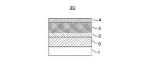
- FIG. 1 is a schematic cross-sectional view showing a first embodiment of a mask blank according to the present invention.
- a mask blank 10 according to the first embodiment of the present invention, an etching stopper film 2 and a light-shielding film 3 that is a pattern forming thin film are laminated in this order on a translucent substrate 1.
- this is a binary mask blank having a structure in which a hard mask film 4 is provided on the light shielding film 3.
- the translucent substrate 1 in the mask blank 10 is not particularly limited as long as it is a substrate used for a transfer mask for manufacturing a semiconductor device.
- the translucent substrate 1 is not particularly limited as long as it is a material having transparency with respect to an exposure wavelength used for pattern exposure transfer onto a semiconductor substrate in the manufacture of a semiconductor device.
- a glass substrate for example, soda lime glass, aluminosilicate glass, etc.
- a synthetic quartz substrate is particularly preferably used because it is highly transparent in an ArF excimer laser (wavelength 193 nm) effective for fine pattern formation or in a shorter wavelength region.
- the etching stopper film 2 needs to be a material having high etching selectivity with the light shielding film 3 directly above.
- a chromium-based material as the material of the etching stopper film 2
- high etching selectivity can be ensured with the light-shielding film 3 made of a silicon-based material or a tantalum-based material.
- the etching stopper film 2 is made of a material containing chromium (Cr), oxygen (O), and carbon (C).
- the etching stopper film 2 has a substantially constant composition. Specifically, it is preferable that the difference in the content of each constituent element in the thickness direction is less than 10 atomic%.
- the etching stopper film 2 has a chromium content of 50 atomic% or more. If the chromium content is 50 atomic% or more, side etching that occurs when patterning the etching stopper film 2 by dry etching under a high bias condition using the light-shielding film 3 on which the transfer pattern is formed as a mask is suppressed. Can do.
- the etching stopper film 2 preferably has a chromium content of 80 atomic% or less.
- the chromium content is more than 80 atomic%, the etching rate when the etching stopper film 2 is patterned by dry etching under a high bias condition is greatly reduced. Therefore, in order to ensure a sufficient etching rate when the etching stopper film 2 is patterned by dry etching under a high bias condition, the etching stopper film 2 has a chromium content of 80 atomic% or less as described above. Is preferred.
- the etching stopper film 2 has a maximum peak of the N1s narrow spectrum obtained by analysis by X-ray photoelectron spectroscopy (XPS) below the detection lower limit. If the N1s narrow spectrum peak exists, Cr—N bonds exist in the chromium-based material forming the etching stopper film 2 in a predetermined ratio or more. If Cr—N bonds are present in a predetermined ratio or more in the material forming the etching stopper film 2, it becomes difficult to suppress the progress of side etching when the etching stopper film 2 is patterned by dry etching under a high bias condition. . In the present invention, it is desirable that the nitrogen (N) content in the etching stopper film 2 is not more than a detection limit value.
- XPS X-ray photoelectron spectroscopy
- the etching stopper film 2 has a maximum peak at a binding energy of 574 eV or less in the narrow spectrum of Cr2p obtained by analysis by X-ray photoelectron spectroscopy.
- a chromium-based material when the narrow spectrum of Cr2p has a maximum peak with a binding energy higher than 574 eV, that is, in a state of chemical shift, chromium bonded to other atoms (particularly nitrogen) It shows that the atomic ratio is high. Since such a chromium-based material tends to have low resistance to dry etching due to a chemical reaction that contributes to etching in the side wall direction of the pattern, it is difficult to suppress the progress of side etching.
- the etching stopper film 2 is formed of a chromium-based material in which the narrow spectrum of Cr2p obtained by analysis by X-ray photoelectron spectroscopy has a maximum peak at a binding energy of 574 eV or less. In this case, it is possible to suppress the progress of side etching when patterning such an etching stopper film 2 by dry etching under a high bias condition.
- the ratio Cc / Ct obtained by dividing the carbon content Cc [atomic%] in the etching stopper film 2 by the total content Ct [atomic%] of chromium, carbon, and oxygen is 0.1 or more. Preferably, it is 0.14 or more.
- the etching stopper film 2 is made of a material containing chromium, oxygen and carbon, and the chromium in the etching stopper film 2 is in the form of Cr—O bond, Cr—C bond, oxygen and carbon. Many exist in any form that is not coupled to any of them.
- a chromium-based material having a high ratio Cc / Ct obtained by dividing the carbon content Cc [atomic%] by the total content Ct [atomic%] of chromium, carbon, and oxygen is the presence of a Cr—C bond in the material.
- the ratio is high, and the progress of side etching when such a chromium-based material is patterned by dry etching under a high bias condition can be suppressed.
- the etching stopper film 2 is made of a material containing chromium, oxygen and carbon, and the total content of these chromium, oxygen and carbon is preferably 95 atomic% or more, more preferably 98 atomic%. That's it.
- the etching stopper film 2 is particularly preferably composed of the above chromium, oxygen and carbon except for impurities which are unavoidably mixed during film formation.
- the impurities inevitably mixed here are elements such as argon, helium, neon, krypton, xenon and hydrogen contained in the sputtering gas when the etching stopper film 2 is formed by sputtering.
- the etching stopper film 2 preferably has an oxygen content of 10 atomic% to 35 atomic%.
- oxygen in such a range in the chromium-based material forming the etching stopper film 2, the etching rate in the case of dry etching under a high bias condition is significantly increased, and the etching time in the film thickness direction is increased. Can be greatly shortened.
- the etching stopper film 2 preferably has a carbon content of 10 atomic% to 20 atomic%. Inclusion of carbon in such a range in the chromium-based material forming the etching stopper film 2 increases the etching rate in the case of dry etching under high bias conditions and suppresses the progress of side etching. Can do.
- the maximum peak of the Si2p narrow spectrum obtained by analysis by X-ray photoelectron spectroscopy is not more than the detection lower limit value.
- the peak of the narrow spectrum of Si2p exists, unbonded silicon and silicon bonded to other atoms are present in a predetermined ratio or more in the material forming the etching stopper film 2.
- the etching stopper film 2 preferably has a silicon content of 1 atomic% or less, and more preferably a detection limit value or less.
- the method for forming the etching stopper film 2 is not particularly limited, but a sputtering film forming method is particularly preferable.
- the sputtering film forming method is preferable because a uniform film having a constant film thickness can be formed. Since the etching stopper film 2 is formed using a highly conductive target, it is more preferable to use DC sputtering with a relatively high deposition rate.
- the thickness of the etching stopper film 2 is not particularly limited, but is preferably in the range of, for example, 3 nm to 20 nm, and more preferably 3.5 nm to 15 nm.
- the light shielding film 3 is made of a material containing one or more elements selected from silicon and tantalum.
- the etching stopper film 2 made of the above-mentioned chromium-based material.
- Examples of a material containing one or more elements selected from silicon and tantalum that form the light-shielding film 3 include the following materials in the present invention.
- Examples of the material containing silicon include a material composed of silicon and nitrogen, or a material containing one or more elements selected from metalloid elements and nonmetallic elements in this material.
- the metalloid element in this case is preferably one or more elements selected from boron, germanium, antimony and tellurium.
- the nonmetallic element includes a nonmetallic element in a narrow sense (nitrogen, carbon, oxygen, phosphorus, sulfur, selenium), a halogen, and a noble gas.
- materials containing silicon suitable for the light-shielding film 3 materials containing one or more elements selected from oxygen, nitrogen, carbon, boron and hydrogen in silicon and transition metals can be cited.
- the transition metal in this case include molybdenum (Mo), tungsten (W), titanium (Ti), tantalum (Ta), zirconium (Zr), hafnium (Hf), niobium (Nb), vanadium (V), Examples include cobalt (Co), nickel (Ni), ruthenium (Ru), tin (Sn), and chromium (Cr).
- Such a material containing silicon and a transition metal has high light shielding performance, and the thickness of the light shielding film 3 can be reduced.
- the material containing tantalum in addition to tantalum metal, a material containing one or more elements selected from nitrogen, oxygen, boron and carbon in tantalum is used.
- a material containing one or more elements selected from nitrogen, oxygen, boron and carbon in tantalum is used.
- Ta, TaN, TaO, TaON, TaBN, TaBO, TaBON, TaCN, TaCO, TaCON, TaBCN, TaBOCN and the like are preferable.
- the method for forming the light shielding film 3 is not particularly limited, and among these, a sputtering film forming method is preferable.
- the sputtering film forming method is preferable because a uniform film having a constant film thickness can be formed.
- the light-shielding film 3 is formed of a material composed of silicon and nitrogen, or a material containing one or more elements selected from a semi-metal element and a non-metal element in this material, the conductivity of the target is low, so that RF (Radio) (Frequency) sputtering or ion beam sputtering is preferable.
- the light-shielding film 3 is formed of a material containing one or more elements selected from oxygen, nitrogen, carbon, boron and hydrogen or a material containing tantalum on silicon and a transition metal, the conductivity of the target is high. Since it is relatively high, it is preferable to form a film using DC sputtering, which has a relatively high film formation speed.
- the light shielding film 3 may have a single layer structure or a laminated structure.
- a two-layer structure of a light-shielding layer and a front-surface antireflection layer, or a three-layer structure further including a back-surface antireflection layer can be used.
- the light-shielding film 3 is required to ensure a predetermined light-shielding property.
- the optical density (OD) with respect to exposure light of an ArF excimer laser (wavelength 193 nm) effective for forming a fine pattern is 2.8 or more. It is calculated
- the thickness of the light-shielding film 3 is not particularly limited, but is preferably 80 nm or less and more preferably 70 nm or less so that a fine pattern can be accurately formed in the binary mask blank.
- the thickness of the light shielding film 3 is preferably 30 nm or more, and preferably 40 nm or more. Is more preferable.
- a hard mask film made of a material having an etching selectivity with respect to the light shielding film 3 is formed on the light shielding film 3.
- (It may be called an “etching mask film”.) 4 is preferably provided.
- the material of the hard mask film 4 functions as an etching mask when a pattern is formed on the light shielding film 3 by dry etching, the material of the hard mask film 4 has sufficient resistance to the dry etching environment of the light shielding film 3. It is necessary to form with material.
- a fluorine-based gas is usually used as an etching gas.
- the material of the hard mask film 4 it is preferable to use a chromium-based material containing chromium having sufficient etching selectivity with the light-shielding film 3 with respect to the dry etching of the fluorine-based gas. .
- the chromium-based material forming the hard mask film 4 examples include a chromium compound obtained by adding one or more elements selected from elements such as oxygen, carbon, nitrogen, hydrogen, and boron to chromium.
- the hard mask film 4 is patterned by dry etching using a mixed gas of chlorine gas and oxygen gas using the pattern of the resist film formed on the surface of the mask blank 10 as a mask. It is preferable that the etching rate in dry etching with a mixed gas with oxygen gas is fast.
- the hard mask film 4 is preferably made of a material containing at least chromium and oxygen.
- the hard mask film 4 is more preferably a single layer film using the same material as the etching stopper film 2. In this case, the surface of the hard mask film 4 on the side opposite to the translucent substrate 1 side and the region in the vicinity thereof are difficult to avoid the progress of oxidation, so that the single layer film having a composition gradient portion with an increased oxygen content and become.
- the method for forming the hard mask film 4 is not particularly limited, but a sputtering film forming method is particularly preferable.
- the sputtering film forming method is preferable because a uniform film having a constant film thickness can be formed. Since the hard mask film 4 is formed using a highly conductive target, it is more preferable to use DC sputtering with a relatively high deposition rate.
- the thickness of the hard mask film 4 is not particularly limited, the hard mask film 4 functions as an etching mask when patterning the light shielding film 3 immediately below by dry etching using a fluorine-based gas. At least a film thickness that does not disappear before the etching of the light shielding film 3 directly below is required. On the other hand, if the hard mask film 4 is too thick, it is difficult to reduce the thickness of the resist film pattern directly above. From such a viewpoint, the film thickness of the hard mask film 4 is preferably in the range of 3 nm to 15 nm, for example, and more preferably 3.5 nm to 10 nm.
- the mask blank of the present invention includes a form having a resist film on the surface of the mask blank 10 having the above configuration.
- the resist film is made of an organic material and is preferably a resist material for electron beam drawing, and a chemically amplified resist material is particularly preferably used.
- the resist film is usually formed on the surface of the mask blank by a coating method such as spin coating.
- the resist film preferably has a thickness of, for example, 200 nm or less from the viewpoint of fine pattern formation. However, by providing the hard mask film 4, the resist film can be made thinner, for example, 100 nm or less. It can be a film thickness.
- the light-shielding layer made of the chromium-based material having the configuration of the present invention, the silicon-based material, or the tantalum-based material is formed on the translucent substrate 1.
- the mask blank of the present invention is particularly suitable when it is required to form a fine pattern (for example, a SRAF (Sub Resolution Assist Features) pattern having a dimension of 50 nm or less) with high pattern accuracy.
- a fine pattern for example, a SRAF (Sub Resolution Assist Features) pattern having a dimension of 50 nm or less
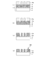
- FIG. 3 is a schematic cross-sectional view showing a manufacturing process of a transfer mask using the mask blank of the first embodiment described above.
- a resist film for electron beam drawing is formed on the surface of the mask blank 10 with a predetermined film thickness by, eg, spin coating.
- a predetermined pattern is drawn on the resist film with an electron beam, developed, and then developed to form a predetermined resist film pattern 6a (see FIG. 3A).
- the resist film pattern 6a has a desired device pattern to be formed on the light-shielding film 3 to be a final transfer pattern.
- a hard mask film pattern 4a is formed on the hard mask film 4 made of a chromium-based material by dry etching using a mixed gas of chlorine-based gas and oxygen gas (FIG. 3 (b)).
- the light shielding film 3 made of a silicon-based material or a tantalum-based material is shielded by dry etching using a fluorine-based gas using the hard mask film pattern 4a as a mask.
- a film pattern 3a is formed (see FIG. 3C).
- the hard mask film pattern 4a is removed by dry etching using a mixed gas of chlorine gas and oxygen gas, and the light shielding film pattern 3a is used as a mask to form the chromium material of the structure of the present invention.
- a pattern 2a is formed on the etching stopper film 2 (see FIG. 3D). In the present invention, in this case, it is preferable to apply the dry etching under the high bias condition described above.
- the mask blank 10 of this embodiment By using the mask blank 10 of this embodiment, side etching that occurs on the pattern side wall of the etching stopper film 2 when the etching stopper film 2 is patterned by dry etching using a mixed gas of chlorine-based gas and oxygen gas is performed. Can be suppressed. As a result, the transfer pattern (the light shielding film pattern 3a) can be prevented from being tilted due to the narrowing of the pattern 2a of the etching stopper film 2, and a fine transfer pattern can be formed with high accuracy.
- the binary transfer mask 20 having the fine light-shielding film pattern 3a to be a transfer pattern on the translucent substrate 1 is completed (see FIG. 3D).
- the transfer mask 20 on which a highly accurate fine transfer pattern is formed can be manufactured.
- the method includes the step of exposing and transferring the transfer pattern of the transfer mask to a resist film on the semiconductor substrate by lithography using the transfer mask 20 manufactured using the mask blank of the present embodiment. According to the semiconductor device manufacturing method, it is possible to manufacture a high-quality semiconductor device in which a device pattern with excellent pattern accuracy is formed.
- the present invention is applied to a binary mask blank, and a binary transfer mask manufactured using the binary mask blank of this embodiment has been described.
- the mask blank of the above-described embodiment is described. It is also possible to manufacture, for example, a substrate digging type phase shift mask (for example, a digging Levenson type phase shift mask, a chromeless phase shift mask, etc.) using a mask blank having the same configuration as in FIG. That is, the mask blank of this embodiment can also be used as a mask blank for producing the phase shift mask.
- FIG. 2 is a schematic cross-sectional view showing a second embodiment of a mask blank according to the present invention.
- the mask blank 30 according to the second embodiment of the present invention is a light-shielding film made of a phase shift film 5, an etching stopper film 2, a silicon-based material or a tantalum-based material on a translucent substrate 1.
- This is a phase shift mask blank having a structure in which a film 3 and a hard mask film 4 made of a chromium-based material are stacked in this order.
- the etching stopper film 2 has the configuration of the present invention. That is, the etching stopper film 2 of the present embodiment is made of a material containing chromium, oxygen and carbon, and the chromium content is 50 atomic% or more. Further, the etching stopper film 2 is formed by X-ray photoelectron spectroscopy. The maximum peak of the N1s narrow spectrum obtained by analyzing with the above is below the detection lower limit value, and the narrow spectrum of Cr2p obtained by analyzing by X-ray photoelectron spectroscopy has the maximum peak with a binding energy of 574 eV or less It is. The details of the etching stopper film 2 of the present embodiment are the same as those in the case of the etching stopper film of the first embodiment described above.
- the details of the translucent substrate 1, the light shielding film 3, and the hard mask film 4 in the mask blank 30 of the present embodiment are the same as in the case of the first embodiment described above. Duplicate explanation is omitted.
- the sputtering film forming method is suitable as in the case of the first embodiment. It is. The film thicknesses of these films are the same as in the case of the first embodiment.
- the laminated structure of the phase shift film 5, the etching stopper film 2, and the light shielding film 3 is used.
- the optical density (OD) with respect to exposure light of an ArF excimer laser (wavelength 193 nm) is required to be 2.8 or more, and more preferably 3.0 or more.
- the phase shift film 5 is formed of a material containing silicon.
- the configuration of the phase shift film 5 applied to the present embodiment is not particularly limited, and has been used, for example, so far.
- the structure of the phase shift film in the phase shift mask can be applied.
- the phase shift film 5 includes, for example, a material containing silicon, a material containing a transition metal and silicon, optical properties (light transmittance, phase difference, etc.), physical properties (etching rate, other films (layers) of the film. In order to improve the etching selectivity between and the like, it is further formed of a material containing at least one element of nitrogen, oxygen and carbon.
- the silicon-containing material examples include silicon nitride, oxide, carbide, oxynitride (oxynitride), carbonate (carbide oxide), and carbonitride (carbonitride oxynitride). ) Is preferred.
- a transition metal silicide composed of a transition metal and silicon, or a transition metal silicide nitride, oxide, carbide, oxynitride, carbonate, or A material containing carbonitride is preferred.
- molybdenum As the transition metal, molybdenum, tantalum, tungsten, titanium, chromium, hafnium, nickel, vanadium, zirconium, ruthenium, rhodium, niobium, and the like are applicable. Of these, molybdenum is particularly preferred.
- the phase shift film 5 can be applied to either a single layer structure or a laminated structure including a low transmittance layer and a high transmittance layer.
- the preferable film thickness of the phase shift film 5 varies depending on the material, but it is desirable to adjust as appropriate from the viewpoint of the phase shift function and light transmittance.
- the thickness of the phase shift film 5 is usually in the range of, for example, 100 nm or less, more preferably 80 nm or less.
- a method for forming the phase shift film 5 is not particularly limited, but a sputtering film forming method is preferable.
- the mask blank of the present invention includes a form having a resist film on the surface of the mask blank 30 having the above-described configuration.
- this resist film it is the same as that of the case of the above-mentioned 1st Embodiment.
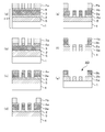
- FIG. 4 is a schematic cross-sectional view showing a manufacturing process of a transfer mask (halftone phase shift mask) using the mask blank 30 of the second embodiment described above.
- a resist film for electron beam drawing is formed on the surface of the mask blank 30 with a predetermined film thickness, for example, by spin coating.
- a predetermined pattern is drawn on the resist film with an electron beam, and after the drawing, development is performed to form a predetermined resist film pattern 7a (see FIG. 4A).
- the resist film pattern 7a has a desired device pattern to be formed on the phase shift film 5 to be a final transfer pattern.
- a hard mask film pattern 4a is formed on the hard mask film 4 made of a chromium-based material by dry etching using a mixed gas of chlorine-based gas and oxygen gas (FIG. 4 (b)).
- the light shielding film 3 made of a silicon-based material or a tantalum-based material is shielded by dry etching using a fluorine-based gas using the hard mask film pattern 4a as a mask.
- a film pattern 3a is formed (see FIG. 4C).
- a resist film similar to the above is formed on the entire surface of the mask blank on which the light shielding film pattern 3a is formed, and a predetermined light shielding pattern (for example, a light shielding band pattern) is drawn on the resist film. Thereafter, development is performed to form a resist film pattern 7b having a predetermined light-shielding pattern on the hard mask film 4 (hard mask film pattern 4a) (see FIG. 4D).
- a predetermined light shielding pattern for example, a light shielding band pattern
- an etching stopper film 2 made of a chromium-based material of the present invention is formed by dry etching using a mixed gas of chlorine-based gas and oxygen gas, using the light-shielding film pattern 3a formed on the light-shielding film 3 as a mask.
- a pattern 2a is formed on the hard mask film 4 using the resist pattern 7b as a mask (see FIG. 4E).
- the phase shift film pattern 5a is formed on the phase shift film 5 by using the pattern 2a formed on the etching stopper film 2 as a mask by dry etching using a fluorine-based gas.
- the hard mask film pattern 4b as a mask, a part of the light shielding film light shielding pattern 3a is removed to form a light shielding film pattern 3b (see FIG. 4F).
- a pattern having a light shielding pattern on the etching stopper film 2 (pattern 2a) using the light shielding film pattern 3b on which the light shielding pattern is formed by dry etching using a mixed gas of chlorine gas and oxygen gas as a mask. 2b is formed and the remaining hard mask film pattern 4b is removed (see FIG. 4G).
- the halftone phase shift mask (transfer mask) 40 including the fine pattern 5a of the phase shift film serving as a transfer pattern and the light-shielding pattern (light-shielding band pattern) in the outer peripheral region on the translucent substrate 1. Is completed (see FIG. 4G).
- the light shielding film pattern 3a formed on the light shielding film 3 is used as a mask, and the etching stopper film 2 is subjected to dry etching using a mixed gas of chlorine gas and oxygen gas. Side etching that occurs on the pattern sidewall of the etching stopper film 2 during patterning (step of FIG. 4E) can be suppressed. As a result, the light shielding film pattern 3a can be prevented from falling due to the narrowing of the pattern 2a of the etching stopper film 2, and even a fine pattern can be formed with high accuracy. Further, by patterning the phase shift film 5 using the pattern 2a of the etching stopper film 2 as a mask (step (f) in FIG. 4), it is possible to form a fine transfer pattern on the phase shift film 5 with high accuracy. Become.
- a transfer mask (halftone phase shift mask) 40 on which a highly accurate fine transfer pattern is formed can be manufactured.
- a semiconductor device including a step of exposing and transferring a transfer pattern of the transfer mask onto a resist film on a semiconductor substrate by lithography using the transfer mask 40 manufactured from the mask blank 30 of the present embodiment. According to this manufacturing method, it is possible to manufacture a high-quality semiconductor device on which a device pattern with excellent pattern accuracy is formed.
- Example 1 relates to manufacture of a mask blank and a transfer mask used for manufacturing a transfer mask (binary mask) using an ArF excimer laser having a wavelength of 193 nm as exposure light, and corresponds to the first embodiment described above.
- the mask blank 10 used in Example 1 has a structure in which an etching stopper film 2, a light shielding film 3, and a hard mask film 4 are laminated in this order on a light transmitting substrate 1 as shown in FIG.
- This mask blank 10 was produced as follows.
- a translucent substrate 1 (size: about 152 mm ⁇ 152 mm ⁇ thickness: about 6.35 mm) made of synthetic quartz glass was prepared.
- the translucent substrate 1 has its main surface and end surfaces polished to a predetermined surface roughness (for example, the main surface has a root mean square roughness Rq of 0.2 nm or less).
- the translucent substrate 1 is installed in a single wafer DC sputtering apparatus, and a target made of chromium is used in a mixed gas atmosphere of argon (Ar), carbon dioxide (CO 2 ), and helium (He).
- argon Ar
- CO 2 carbon dioxide
- He helium
- an etching stopper film 2 made of a CrOC film containing chromium, oxygen and carbon was formed to a thickness of 10 nm on the main surface of the translucent substrate 1.
- a lower layer of a light shielding film made of (Mo: 9.2 atomic%, Si: 68.3 atomic%, N: 22.5 atomic%) was formed to a thickness of 47 nm.
- a MoSiN film containing molybdenum, silicon and nitrogen is formed on the lower layer of the light shielding film by DC sputtering using a mixed gas of nitrogen (N 2 ) and argon (Ar).
- the upper layer of the light-shielding film made of Mo: 5.8 atomic%, Si: 64.4 atomic%, and N: 27.7 atomic% was formed to a thickness of 4 nm.
- a MoSi-based light shielding film 3 having a two-layer structure with a total thickness of 51 nm was formed.
- the optical density of the laminated film of the formed MoSi-based light shielding film 3 was 3.0 or more at the wavelength of ArF excimer laser (193 nm).
- the translucent substrate 1 on which the etching stopper film 2 and the light-shielding film 3 are formed is placed in a single wafer DC sputtering apparatus, and a target made of chromium is used to make argon (Ar) and carbon dioxide (CO 2 ). ) And helium (He) mixed gas under the same film forming conditions as those for forming the etching stopper film 2, so that the surface of the light shielding film 3 contains CrOC containing chromium, oxygen and carbon.
- a hard mask film 4 made of a film was formed with a thickness of 10 nm.
- the mask blank 10 of Example 1 was produced as described above.
- a material in which only the etching stopper film 2 was formed on the main surface of another translucent substrate under the same conditions as described above was prepared.
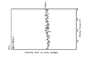
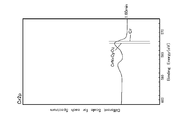
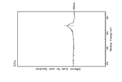
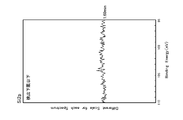
- the etching stopper film 2 was analyzed by X-ray photoelectron spectroscopy (with RBS (Rutherford Backscattering Spectrometry) correction). As a result, it was confirmed that the content of each constituent element in the etching stopper film 2 was an average value of Cr: 71 atomic%, O: 15 atomic%, and C: 14 atomic%. Further, the difference in the content of each constituent element in the thickness direction of the etching stopper film 2 is 3 atomic% or less (however, the region near the surface of the etching stopper film 2 whose analysis results are affected by the atmosphere is excluded.
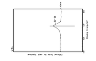
- FIG. 6 shows the results of the chemical direction analysis of the O1s narrow spectrum in the depth direction
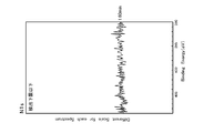
- FIG. 7 shows the results of the chemical direction analysis of the N1s narrow spectrum in the depth direction
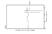
- FIG. 8 shows the depth direction of the C1s narrow spectrum.
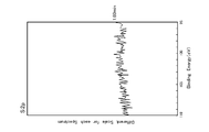
- the result of chemical bonding state analysis is shown in FIG. 9, and the result of chemical bonding state analysis in the depth direction of the Si2p narrow spectrum is shown in FIG.
- X-rays are irradiated toward the surface of the etching stopper film 2 to measure the energy distribution of photoelectrons emitted from the etching stopper film 2, and then Ar gas.
- Example 1 the analysis by the X-ray photoelectron spectroscopy uses monochromatic Al (1486.6 eV) as the X-ray source, the photoelectron detection region is 100 ⁇ m ⁇ , and the detection depth is about 4 to 5 nm ( The extraction angle was 45 degrees) (the same applies to the following examples and comparative examples).
- the position in the film thickness direction of the etching stopper film 2 after being dug by Ar gas sputtering from the outermost surface of the etching stopper film 2 by 1.60 min is a position having a depth of about 6 nm from the surface.
- the plot of “60 min” is the measurement result at the position of the depth.
- the scale of the vertical axis in each narrow spectrum of FIGS. 6 to 10 is not the same.
- the N1s narrow spectrum in FIG. 8 and the Si2p narrow spectrum in FIG. 10 are greatly expanded in scale on the vertical axis as compared with the narrow spectra in FIG. 6, FIG. 7 and FIG. Therefore, the vibration wave in the N1s narrow spectrum of FIG. 8 and the Si2p narrow spectrum of FIG. 10 does not show the presence of a peak but only shows noise.
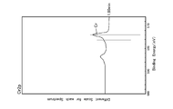
- the etching stopper film 2 of Example 1 has a maximum peak at a binding energy of 574 eV. This result means that in the etching stopper film 2, atoms such as oxygen and unbonded chromium atoms are present in a certain ratio or more.
- Example 7 shows that the etching stopper film 2 of Example 1 has a maximum peak at a binding energy of about 530 eV from the result of the O1s narrow spectrum in FIG. This result means that the etching stopper film 2 has a Cr—O bond of a certain ratio or more.
- the etching stopper film 2 of Example 1 has the maximum peak at a binding energy of 282 eV to 283 eV. This result means that in the etching stopper film 2, Cr—C bonds exist in a certain ratio or more.
- a transfer mask (binary mask) was manufactured using the mask blank 10 according to the manufacturing process shown in FIG.
- the following symbols correspond to the symbols in FIG.
- a chemical amplification resist for electron beam drawing PRL009 manufactured by Fuji Film Electronics Materials Co., Ltd.
- PRL009 manufactured by Fuji Film Electronics Materials Co., Ltd.
- a predetermined baking process is performed, so that the film thickness is 80 nm.
- a resist film was formed.
- the resist film is developed to form a resist film pattern. 6a was formed (see FIG. 3A).
- the resist film pattern 6a includes an SRAF pattern having a line width of 50 nm.
- the hard mask film 4 was dry-etched by dry etching under the above-described high bias condition to form a hard mask film pattern 4a (see FIG. 3B).
- the MoSi-based light shielding film 3 having a two-layer structure is continuously subjected to dry etching to form the light shielding film pattern 3a ( (Refer FIG.3 (c)).
- a fluorine-based gas SF 6
- SF 6 fluorine-based gas
- the etching stopper film 2 is etched using the light shielding film pattern 3a as a mask to form a pattern 2a on the etching stopper film 2, and the hard mask film pattern 4a is It removed (refer FIG.3 (d)).
- the transfer mask 20 of Example 1 is separately manufactured, a cross-sectional STEM (Scanning Transmission Electron Microscope) image of the region where the SRAF pattern is formed is obtained, and the light shielding film pattern 3a and the etching stopper film are obtained. The line width of each pattern 2a was measured.
- the etching bias which is the amount of change between the line width of the light shielding film pattern 3a and the line width of the pattern 2a of the etching stopper film.
- the etching bias was about 6 nm, which was much smaller than that in the case of dry etching for a conventional chromium-based material film.
- the pattern of the etching stopper film 2 is used even when the etching stopper film 2 is patterned by dry etching under a high bias condition using the light shielding film pattern 3a as a mask and using a mixed gas of chlorine gas and oxygen gas. It shows that side etching occurring on the side wall can be suppressed. In addition, this makes it possible to suppress the tilting of the light-shielding film pattern 3a due to the thinning of the pattern 2a of the etching stopper film 2. For example, even a transfer pattern having a fine pattern such as an SRAF pattern with a line width of 50 nm or less is accurate. It shows that it can be formed well.
- the transfer mask 20 on which a highly accurate fine transfer pattern is formed can be manufactured.
- an exposure transfer image was simulated when the transfer mask 20 was exposed and transferred to a resist film on a semiconductor device with exposure light having a wavelength of 193 nm using AIMS 193 (manufactured by Carl Zeiss).
- AIMS 193 manufactured by Carl Zeiss
- the design specifications were sufficiently satisfied. From the above, when the transfer mask 20 manufactured from the mask blank of Example 1 is set in an exposure apparatus and subjected to exposure transfer with exposure light of an ArF excimer laser, it is applied to the resist film on the semiconductor device. It can be said that exposure transfer can be performed with high accuracy.
- Example 2 The mask blank 10 of Example 2 was produced in the same manner as Example 1 except for the etching stopper film 2.
- the etching stopper film 2 in Example 2 was formed by changing the film forming conditions as compared with the etching stopper film 2 of Example 1 as follows.
- the same translucent substrate 1 as in Example 1 is installed, and a target made of chromium is used, and argon (Ar), carbon dioxide (CO 2 ), and helium ( By performing reactive sputtering in a mixed gas atmosphere of He), an etching stopper film 2 made of a CrOC film containing chromium, oxygen, and carbon is formed on the main surface of the translucent substrate 1 with a thickness of 10 nm. Formed. Next, a MoSi light-shielding film 3 was formed on the etching stopper film 2 under the same conditions as in Example 1.
- the translucent substrate 1 on which the etching stopper film 2 and the light-shielding film 3 are formed is placed in a single wafer DC sputtering apparatus, and a target made of chromium is used to make argon (Ar) and carbon dioxide (CO 2 ). ) And helium (He) mixed gas is sputtered under the same film forming conditions as those for forming the etching stopper film 2 of Example 2, so that chromium, oxygen and carbon are formed on the surface of the light shielding film 3.
- a hard mask film 4 made of a CrOC film containing bismuth was formed with a thickness of 10 nm.
- the mask blank 10 of Example 2 was produced as described above.
- etching stopper film 2 of Example 2 was analyzed by X-ray photoelectron spectroscopy (with RBS correction). As a result, it was confirmed that the content of each constituent element in the etching stopper film 2 was, on average, Cr: 55 atomic%, O: 30 atomic%, and C: 15 atomic%. Further, the difference in the content of each constituent element in the thickness direction of the etching stopper film 2 is 3 atomic% or less (however, the region near the surface of the etching stopper film 2 whose analysis results are affected by the atmosphere is excluded.
- FIG. 11 shows the results of the chemical direction analysis of the depth direction of FIG. 11
- FIG. 12 shows the results of the chemical state analysis of the depth direction of the O1s narrow spectrum
- FIG. 13 shows the results of the chemical direction analysis of the N1s narrow spectrum
- FIG. 14 shows the results of the chemical direction analysis in the depth direction of the C1s narrow spectrum
- FIG. 15 shows the results of the chemical direction analysis in the depth direction of the Si2p narrow spectrum.
- the scale of the vertical axis in each narrow spectrum in FIGS. 11 to 15 is not the same.
- the N1s narrow spectrum of FIG. 13 and the Si2p narrow spectrum of FIG. 15 are greatly expanded in scale on the vertical axis as compared with the narrow spectra of FIGS. Therefore, the vibration wave in the N1s narrow spectrum of FIG. 13 and the Si2p narrow spectrum of FIG. 15 does not show the presence of a peak but only shows noise.
- the etching stopper film 2 of Example 2 has a maximum peak at a binding energy of 574 eV. This result means that in the etching stopper film 2, atoms such as oxygen and unbonded chromium atoms are present in a certain ratio or more.
- the etching stopper film 2 of Example 2 has a maximum peak at a binding energy of about 530 eV. This result means that the etching stopper film 2 has a Cr—O bond of a certain ratio or more.
- the etching stopper film 2 of Example 2 has a maximum peak at a binding energy of 282 eV to 283 eV from the result of the C1s narrow spectrum in FIG. This result means that in the etching stopper film 2, Cr—C bonds exist in a certain ratio or more.
- the pattern 2a of the etching stopper film 2 and the light-shielding film pattern 3a are laminated on the translucent substrate 1 according to the same manufacturing process as in Example 1 described above.
- a transfer mask (binary mask) 20 having a transfer pattern was manufactured.
- the transfer mask 20 of the second embodiment is manufactured separately in the same procedure as the first embodiment, a cross-sectional STEM image of the region where the SRAF pattern is formed is obtained, and the pattern of the light shielding film pattern 3a and the etching stopper film 2 is obtained. Each line width of 2a was measured.
- the etching bias is about 10 nm. The value was much smaller than in the case of dry etching on the film.
- Example 2 exposure was performed when the transfer mask 20 of Example 2 was exposed and transferred to the resist film on the semiconductor device with exposure light having a wavelength of 193 nm using AIMS 193 (manufactured by Carl Zeiss) as in Example 1.
- the transfer image was simulated. When the exposure transfer image obtained by this simulation was verified, the design specifications were sufficiently satisfied. From the above, when the transfer mask 20 manufactured from the mask blank of Example 2 is set in an exposure apparatus and subjected to exposure transfer with exposure light of an ArF excimer laser, the transfer mask 20 is higher than the resist film on the semiconductor device. It can be said that exposure transfer can be performed with high accuracy.
- Example 3 relates to manufacture of a mask blank and a halftone phase shift mask (transfer mask) used for manufacturing a halftone phase shift mask (transfer mask) using an ArF excimer laser with a wavelength of 193 nm as exposure light.
- a mask blank 30 used in Example 3 is formed by laminating a phase shift film 5, an etching stopper film 2, a light shielding film 3, and a hard mask film 4 in this order on a light transmitting substrate 1 as shown in FIG. Of structure.
- This mask blank 30 was produced as follows.
- a MoSiN film (Mo: 4.1 atomic%, Si: 35.6 atomic%, N: 60.3) containing molybdenum, silicon, and nitrogen is formed on the surface of the translucent substrate 1 by sputtering using a sputtering gas.
- a phase shift film 5 composed of 69% of atomic percent was formed.
- the translucent substrate 1 on which the phase shift film 5 was formed was taken out of the sputtering apparatus, and the phase shift film 5 on the translucent substrate was subjected to a heat treatment in the atmosphere.
- This heat treatment was performed at 450 ° C. for 30 minutes.
- the transmittance is 6.44% and the phase The shift amount was 174.3 degrees.
- the translucent substrate on which the phase shift film 5 is formed is again introduced into the sputtering apparatus, and the CrOC film of Example 1 is formed on the phase shift film 5 under the same film formation conditions as in Example 1.
- the mask blank 30 of Example 3 was produced as described above.
- a halftone phase shift mask was manufactured using the mask blank 30 according to the manufacturing process shown in FIG.
- the following symbols correspond to the symbols in FIG.
- a chemical amplification resist for electron beam drawing PRL009 manufactured by Fuji Film Electronics Materials Co., Ltd.
- PRL009 manufactured by Fuji Film Electronics Materials Co., Ltd.
- a predetermined baking process is performed, so that the film thickness is 80 nm.
- a resist film was formed.
- the resist film is developed to form a resist film A pattern 7a was formed (see FIG. 4A).
- the resist film pattern 7a includes a SRAF pattern having a line width (50 nm).
- the hard mask film 4 was dry-etched by dry etching under the above-described high bias condition to form a hard mask film pattern 4a (see FIG. 4B).
- etching of the MoSi-based light shielding film 3 is continuously performed by dry etching using a fluorine-based gas using the hard mask film pattern 4a as a mask.
- a light shielding film pattern 3a was formed (see FIG. 4C).
- a fluorine-based gas SF 6
- SF 6 fluorine-based gas
- a resist film similar to the above is formed on the entire surface of the mask blank on which the light shielding film pattern 3a is formed, and a predetermined light shielding pattern (light shielding band pattern) is drawn on the resist film.
- a resist film pattern 7b having a predetermined light shielding pattern was formed on the hard mask film 4 (hard mask film pattern 4a) (see FIG. 4D).
- the pattern 2a is formed on the etching stopper film 2 made of a chromium material having the structure of the present invention using the light shielding film pattern 3a as a mask.
- a pattern 4b having the light shielding pattern was formed on the hard mask film 4 (see FIG. 4E).
- the phase shift film pattern 5a is formed on the phase shift film 5 by dry etching using a fluorine-based gas using the pattern 2a formed on the etching stopper film 2 as a mask.
- a fluorine-based gas SF 6
- SF 6 fluorine-based gas
- the light shielding in which the light shielding pattern is formed by dry etching using a mixed gas (Cl 2 : O 2 4: 1 (flow rate ratio)) of chlorine gas (Cl 2 ) and oxygen gas (O 2 ).
- chlorine gas Cl 2
- oxygen gas O 2
- the halftone phase shift mask (transfer mask) 40 having the phase shift film pattern 5a as a transfer pattern and the light shielding pattern (light shielding band pattern) in the outer peripheral region on the translucent substrate 1 is completed. (See FIG. 4 (g)). As a result of inspecting the obtained phase shift mask 40 with a mask inspection apparatus using a mask inspection apparatus, it was confirmed that the fine pattern of the phase shift film was formed within the allowable range from the design value.
- the light shielding film pattern 3a formed on the light shielding film 3 is used as a mask, and the etching stopper film 2 is dry-etched using a mixed gas of chlorine-based gas and oxygen gas. Since side etching occurring on the pattern side wall of the etching stopper film 2 during patterning (step of FIG. 4E) can be suppressed, and the fall of the light shielding film pattern 3a due to the narrowing of the pattern 2a of the etching stopper film 2 can be suppressed. Even a fine light-shielding film pattern (transfer pattern) can be formed with high accuracy.
- phase shift film 5 is formed using the pattern 2a of the etching stopper film 2 without a narrow pattern width by side etching as a mask (step of FIG. 4 (f)).
- a fine transfer pattern is also formed on the phase shift film 5. Can be formed with high accuracy.
- phase shift mask 40 manufactured from the mask blank of Example 3 can perform exposure transfer on the resist film on the semiconductor device with high accuracy.
- Example 4 relates to the manufacture of a substrate digging type phase shift mask (chromeless phase shift mask) using a mask blank having the same configuration as the mask blank 10 of Example 1, and the manufacturing process shown in FIG. It explains according to.
- the mask blank used in Example 4 has a structure in which an etching stopper film 2, a light-shielding film 3, and a hard mask film 4 are laminated in this order on a translucent substrate 1, and was produced as follows. .
- a translucent substrate 1 (synthetic quartz substrate) prepared in the same manner as in Example 1 was placed in a single-wafer DC sputtering apparatus, and the same film forming conditions as in Example 1 were applied on the substrate.
- An etching stopper film 2 made of a CrOC film was formed.
- a two-layered MoSi-based light-shielding film 3 of a lower layer 31 of the MoSiN film and an upper layer 32 of the MoSiN film was formed on the etching stopper film 2 under the same film formation conditions as in Example 1.
- a hard mask film 4 made of a CrOC film was formed on the light shielding film 3 under the same film forming conditions as in Example 1.
- the mask blank of Example 4 was produced as described above.
- a phase shift mask was manufactured using the mask blank of Example 4 according to the manufacturing process shown in FIG.
- a chemical amplification resist for electron beam drawing PRL009 manufactured by Fuji Film Electronics Materials Co., Ltd.
- PRL009 manufactured by Fuji Film Electronics Materials Co., Ltd.
- a predetermined baking process is performed to form a resist having a thickness of 80 nm.
- a film was formed.
- a predetermined device pattern (a pattern corresponding to a transfer pattern dug into the substrate) is drawn on the resist film using an electron beam drawing machine, and then the resist film is developed to form a resist film pattern 8a.
- the resist film pattern 8a includes a line and space pattern having a line width of 50 nm.
- the hard mask film 4 was dry-etched by dry etching under the above-described high bias condition to form a hard mask film pattern 4a (see FIG. 5B).
- dry etching of the light-shielding film 3 having a two-layer structure of MoSi is performed by using the hard mask film pattern 4a as a mask and using a fluorine-based gas (SF 6 ) as an etching gas. It performed continuously and formed the light shielding film pattern 3a (refer FIG.5 (c)).
- SF 6 fluorine-based gas
- dry etching of the etching stopper film 2 is performed by dry etching under the above-described high bias condition using the light shielding film pattern 3a as a mask to form a pattern 2a on the etching stopper film 2, and the hard mask film pattern 4a.
- a resist film similar to the above is formed on the entire surface of the mask blank on which the light shielding film pattern 3a is formed, and a predetermined light shielding pattern (light shielding band pattern) is drawn on the resist film.
- a resist film pattern 8b having a light shielding pattern was formed (see FIG. 5E).
- the exposed light shielding film pattern 3a is peeled and removed by dry etching using a fluorine-based gas, and the pattern 2a formed on the etching stopper film 2 is used as a mask.
- the light-transmitting substrate 1 synthetic quartz substrate
- the translucent substrate was dug to a depth (about 173 nm) at which a phase difference of 180 degrees was obtained.
- a mixed gas of fluorine-based gas (CF 4 ) and helium (He) was used as an etching gas for dry etching.
- the digging type phase shift pattern 1a is formed on the translucent substrate 1, and the digging type phase shift mask (transfer mask) having the light shielding pattern (light shielding band pattern) in the outer peripheral region is formed. ) 50 was completed (see FIG. 5G). As a result of inspecting the obtained phase shift mask 50 with a mask inspection apparatus using a mask inspection apparatus, it was confirmed that the phase shift pattern was formed within the allowable range from the design value.
- Example 4 when the light shielding film pattern 3a formed on the light shielding film 3 is used as a mask, the etching stopper film 2 is patterned by dry etching using a mixed gas of chlorine-based gas and oxygen gas (FIG. Side etching that occurs on the pattern side wall of the etching stopper film 2 in step (d) can be suppressed, and the fall of the light shielding film pattern 3a due to the narrowing of the pattern 2a of the etching stopper film 2 can be suppressed. Further, the substrate is dug using the pattern 2a of the etching stopper film 2 with no pattern width narrowed by side etching as a mask (step of FIG. 5 (f)), so that a fine phase shift pattern can be accurately formed by dug the substrate. can do.
- phase shift mask 50 manufactured from the mask blank of Example 4 can perform exposure transfer on the resist film on the semiconductor device with high accuracy.
- Comparative Example 1 The mask blank of Comparative Example 1 was produced in the same manner as Example 1 except for the etching stopper film.
- the etching stopper film in Comparative Example 1 was formed by changing the film formation conditions as compared with the etching stopper film 2 of Example 1 as follows. Specifically, the same translucent substrate (synthetic quartz substrate) as in Example 1 above is installed in a single wafer DC sputtering apparatus, and a target made of chromium is used, and argon (Ar) and carbon dioxide (CO 2 ).
- etching stopper film of Comparative Example 1 was analyzed by X-ray photoelectron spectroscopy (with RBS correction). As a result, the content of each constituent element in the etching stopper film of Comparative Example 1 is, on average, Cr: 55 atomic%, O: 22 atomic%, C: 12 atomic%, and N: 11 atomic%. It could be confirmed.
- the difference in the content of each constituent element in the thickness direction of the etching stopper film is 3 atomic% or less (except for the area near the surface of the etching stopper film whose analysis results are affected by the atmosphere). It was confirmed that there was substantially no composition gradient in the thickness direction.
- FIG. 16 shows the results of the chemical analysis of the chemical direction in the depth direction of the Cr2p narrow spectrum obtained as a result of the X-ray photoelectron spectroscopy analysis of the etching stopper film in Comparative Example 1.
- FIG. 17 shows the result of the chemical direction analysis of the O1s narrow spectrum in the depth direction
- FIG. 18 shows the result of the chemical direction analysis of the depth direction of the N1s narrow spectrum
- FIG. 19 shows the results of analysis of the chemical bonding state in the depth direction of the Si2p narrow spectrum, respectively.
- the etching stopper film of Comparative Example 1 has a maximum peak at a binding energy of about 530 eV. This result means that Cr—O bonds are present in a certain ratio or more.
- a transfer mask (binary mask) of Comparative Example 1 was manufactured according to the same manufacturing process as in Example 1 described above. Further, in the same procedure as in Example 1, the transfer mask of Comparative Example 1 is separately manufactured, a cross-sectional STEM image of the region where the SRAF pattern is formed is obtained, and the pattern of the light shielding film pattern and the etching stopper film is obtained. Each line width was measured.
- the etching bias is 27 nm, and dry etching with respect to a conventional chromium-based material film is performed. As in the case of, it was a relatively large value.
- etching is performed when the etching stopper film is patterned by dry etching under a high bias condition using the light shielding film pattern as a mask and using a mixed gas of chlorine gas and oxygen gas. It is difficult to suppress the side etching that occurs on the pattern sidewall of the stopper film, so that the light shielding film pattern collapses due to the narrowing of the etching stopper film pattern. For example, it is possible to accurately form a fine transfer pattern with a line width of 50 nm or less. It is difficult.
- Comparative Example 2 The mask blank of Comparative Example 2 was produced in the same manner as Example 1 except for the etching stopper film.
- the etching stopper film in Comparative Example 2 was formed by changing the film forming conditions as compared with the etching stopper film of Example 1 as follows. Specifically, in the single-wafer DC sputtering apparatus, the same translucent substrate as in Example 1 is installed, and a target made of chromium is used, and argon (Ar), nitric oxide (NO), and helium (He) are used. In the mixed gas atmosphere, an etching stopper film made of a CrON film containing chromium, oxygen and nitrogen was formed to a thickness of 10 nm on the main surface of the translucent substrate. Next, the MoSi light-shielding film 3 and the hard mask film 4 of Example 1 were sequentially formed on the etching stopper film under the same conditions as in Example 1. As described above, a mask blank of Comparative Example 2 was produced.
- the etching stopper film of Comparative Example 2 was analyzed by X-ray photoelectron spectroscopy (with RBS correction). As a result, it was confirmed that the content of each constituent element in the etching stopper film of Comparative Example 2 was Cr: 58 atomic%, O: 17 atomic%, and N: 25 atomic% on average. Further, the difference in the content of each constituent element in the thickness direction of the etching stopper film is 3 atomic% or less (except for the area near the surface of the etching stopper film whose analysis results are affected by the atmosphere). It was confirmed that there was substantially no composition gradient in the thickness direction.
- the etching stopper film of Comparative Example 2 was analyzed by X-ray photoelectron spectroscopy, and as a result of the chemical direction analysis of the Cr2p narrow spectrum in the depth direction, the O1s narrow spectrum was analyzed in the depth direction.
- a binary transfer mask of Comparative Example 2 was manufactured according to the same manufacturing process as in Example 1 described above. Further, in the same procedure as in Example 1, the transfer mask of Comparative Example 2 is separately manufactured, a cross-sectional STEM image of the region where the SRAF pattern is formed is obtained, and the light shielding film pattern and the etching stopper film pattern are obtained. Each line width was measured.
- an etching bias which is a change amount between the line width of the light shielding film pattern and the line width of the etching stopper film pattern, is calculated. Further, as a result of calculating the etching bias, the etching bias is 30 nm. Compared with the case of dry etching for a chromium-based material film, the value was much larger.
Abstract
In the present invention, an etching stopper film (2), a light-blocking film (3) comprising a material containing one or more elements selected from among silicon and tantalum, and a hard mask film (4) are laminated in that order on a translucent substrate (1). The etching stopper film is made of a material containing chromium, oxygen and carbon, the chromium content is 50 atom% or more, the maximum peak in a N1s narrow spectrum obtained by means of analysis using X-Ray photoelectron spectroscopy is below the detection limit, and a Cr2p narrow spectrum obtained by means of analysis using X-Ray photoelectron spectroscopy has a maximum peak at a bond energy of 574 eV or less.
Description
本発明は、マスクブランク、該マスクブランクを用いる転写用マスクの製造方法、及び該製造方法により製造された転写用マスクを用いる半導体デバイスの製造方法に関する。本発明は特に、波長200nm以下の短波長の露光光を露光光源とする露光装置に好適に用いられるマスクブランク、転写用マスクの製造方法、及び半導体デバイスの製造方法に関する。
The present invention relates to a mask blank, a method for manufacturing a transfer mask using the mask blank, and a method for manufacturing a semiconductor device using the transfer mask manufactured by the manufacturing method. In particular, the present invention relates to a mask blank, a transfer mask manufacturing method, and a semiconductor device manufacturing method that are preferably used in an exposure apparatus that uses exposure light having a short wavelength of 200 nm or less as an exposure light source.
一般に、半導体デバイスの製造工程では、フォトリソグラフィー法を用いて微細パターンの形成が行われている。また、この微細パターンの形成には通常何枚もの転写用マスク(フォトマスク)と呼ばれている基板が使用される。この転写用マスクは、一般に透光性のガラス基板上に、金属薄膜等からなる微細パターンを設けたものである。この転写用マスクの製造においてもフォトリソグラフィー法が用いられている。
Generally, in a semiconductor device manufacturing process, a fine pattern is formed using a photolithography method. In addition, a number of substrates called transfer masks (photomasks) are usually used for forming this fine pattern. This transfer mask is generally a transparent glass substrate provided with a fine pattern made of a metal thin film or the like. A photolithography method is also used in the production of the transfer mask.
この転写用マスクは同じ微細パターンを大量に転写するための原版となるため、転写用マスク上に形成されたパターンの寸法精度は、この転写用マスクを用いて作製される微細パターンの寸法精度に直接影響する。近年、半導体デバイスのパターンの微細化が著しく進んできており、それに応じて転写用マスクに形成されるマスクパターンの微細化に加え、そのパターン精度もより高いものが要求されている。他方、転写用マスクのパターンの微細化に加え、フォトリソグラフィーで使用される露光光源波長の短波長化が進んでいる。具体的には、半導体デバイス製造の際の露光光源としては、近年ではKrFエキシマレーザー(波長248nm)から、200nm以下の波長、例えばArFエキシマレーザー(波長193nm)へと短波長化が進んでいる。
Since this transfer mask serves as a master for transferring a large amount of the same fine pattern, the dimensional accuracy of the pattern formed on the transfer mask is the same as the dimensional accuracy of the fine pattern produced using this transfer mask. Directly affects. In recent years, the miniaturization of semiconductor device patterns has been remarkably advanced, and accordingly, in addition to the miniaturization of mask patterns formed on transfer masks, higher pattern accuracy is required. On the other hand, in addition to miniaturization of the pattern of the transfer mask, the exposure light source wavelength used in photolithography has been shortened. Specifically, as an exposure light source for manufacturing semiconductor devices, in recent years, the wavelength has been shortened from a KrF excimer laser (wavelength 248 nm) to a wavelength of 200 nm or less, for example, an ArF excimer laser (wavelength 193 nm).
また、転写用マスクの種類としては、従来の透光性基板上にクロム系材料からなる遮光膜パターンを有するバイナリマスクのほかに、ハーフトーン型位相シフトマスクが知られている。このハーフトーン型位相シフトマスクは、透光性基板上に光半透過膜パターンを備えたものである。そして、この光半透過膜(ハーフトーン型位相シフト膜)は、実質的に露光に寄与しない強度で光を透過させ、かつその光半透過膜を透過した光に、同じ距離だけ空気中を透過した光に対して所定の位相差を生じさせる機能を有しており、これにより、いわゆる位相シフト効果を生じさせている。
As a type of transfer mask, a halftone phase shift mask is known in addition to a binary mask having a light-shielding film pattern made of a chromium-based material on a conventional translucent substrate. This halftone phase shift mask is provided with a light semi-transmissive film pattern on a light-transmitting substrate. This light semi-transmissive film (halftone phase shift film) transmits light at an intensity that does not substantially contribute to exposure, and transmits the light transmitted through the light semi-transmissive film through the air for the same distance. It has a function of generating a predetermined phase difference with respect to the emitted light, thereby generating a so-called phase shift effect.
近年では、透光性基板上に、ケイ素系材料やタンタル系材料からなる遮光膜を有するバイナリマスクブランクなども出現している。また、位相シフト膜上に、遷移金属とケイ素を含有する材料からなる遮光膜を設けた位相シフトマスクブランクも知られている(特許文献1)。この位相シフトマスクブランクでは、位相シフト膜を形成する材料にも遷移金属とケイ素を含有する材料が適用されている。そのため、位相シフト膜と遮光膜との間でドライエッチングに対するエッチング選択性を確保することが難しい。そこで、特許文献1に開示された位相シフトマスクブランクでは、位相シフト膜と遮光膜との間にクロム系材料からなるエッチングストッパー膜を設けている。
In recent years, binary mask blanks having a light-shielding film made of a silicon-based material or a tantalum-based material on a light-transmitting substrate have also appeared. There is also known a phase shift mask blank in which a light shielding film made of a material containing a transition metal and silicon is provided on a phase shift film (Patent Document 1). In this phase shift mask blank, a material containing a transition metal and silicon is also applied to the material forming the phase shift film. Therefore, it is difficult to ensure etching selectivity for dry etching between the phase shift film and the light shielding film. Therefore, in the phase shift mask blank disclosed in Patent Document 1, an etching stopper film made of a chromium-based material is provided between the phase shift film and the light shielding film.
また、上記の透光性基板上にケイ素系材料やタンタル系材料からなる遮光膜を有するバイナリマスクブランクにおいても、例えば透光性基板として用いるガラス基板と遮光膜との間でドライエッチングに対するエッチング選択性を確保することが容易ではなく、ガラス基板と遮光膜との間にクロム系材料からなるエッチングストッパー膜を設けることがある。
In addition, even in a binary mask blank having a light-shielding film made of a silicon-based material or a tantalum-based material on the light-transmitting substrate, for example, an etching selection for dry etching between a glass substrate used as a light-transmitting substrate and the light-shielding film. It is not easy to ensure the property, and an etching stopper film made of a chromium-based material may be provided between the glass substrate and the light shielding film.
例えば上記のような透光性基板(ガラス基板)上に、クロム系材料からなるエッチングストッパー膜及びケイ素系材料またはタンタル系材料からなる遮光膜がこの順に積層された構造のマスクブランクを用いて転写用マスク(バイナリマスク)を作製するには、以下の工程を実行する。まず、マスクブランクの表面に形成した転写パターン(この転写パターンとは、遮光膜に形成すべきパターンのことである。)を有するレジスト膜をマスクとし、フッ素系ガスを用いたドライエッチングにより、上記遮光膜に転写パターンを形成する。次いで、この転写パターンが形成された遮光膜をマスクとし、塩素系ガスと酸素ガスとの混合ガスを用いたドライエッチングにより、上記エッチングストッパー膜に転写パターンを形成する。こうして、透光性基板上にケイ素系材料またはタンタル系材料からなる遮光膜パターンを有する転写用マスクが出来上がる。
For example, transfer is performed using a mask blank having a structure in which an etching stopper film made of a chromium-based material and a light-shielding film made of a silicon-based material or a tantalum-based material are laminated in this order on a light-transmitting substrate (glass substrate) as described above. In order to manufacture a mask (binary mask), the following steps are executed. First, a resist film having a transfer pattern formed on the surface of the mask blank (this transfer pattern is a pattern to be formed on the light-shielding film) is used as a mask, and dry etching using a fluorine-based gas is performed. A transfer pattern is formed on the light shielding film. Next, a transfer pattern is formed on the etching stopper film by dry etching using a mixed gas of chlorine-based gas and oxygen gas using the light-shielding film on which the transfer pattern is formed as a mask. Thus, a transfer mask having a light-shielding film pattern made of a silicon-based material or a tantalum-based material on the translucent substrate is completed.
上記のとおり、転写パターンが形成された遮光膜をマスクとし、塩素系ガスと酸素ガスとの混合ガスを用いたドライエッチングにより、上記クロム系材料のエッチングストッパー膜に転写パターンが形成されるが、この塩素系ガスと酸素ガスとの混合ガスをエッチングガスに用いるドライエッチングは、異方性エッチングの傾向が小さく、等方性エッチングの傾向が大きい。一般に、ドライエッチングによって薄膜にパターンを形成する場合、薄膜の厚さ方向のエッチングのみならず、薄膜に形成されるパターンの側壁方向へのエッチング、所謂サイドエッチングが進む。このサイドエッチングの進行を抑制するために、ドライエッチングの際、薄膜が形成されている透光性基板の主表面の反対側からバイアス電圧を印加し、エッチングガスが膜の厚さ方向により多く接触するように制御することがこれまでも行われていた。上記遮光膜のドライエッチングに適用するフッ素系ガスのようにイオン性のプラズマになる傾向が大きいエッチングガスを用いるイオン主体のドライエッチングの場合には、バイアス電圧を印加することによるエッチング方向の制御性が高く、エッチングの異方性が高められるため、エッチングされる薄膜のサイドエッチング量を微小にできる。一方、塩素系ガスと酸素ガスとの混合ガスによるドライエッチングの場合、酸素ガスはラジカル性のプラズマになる傾向が高いため、バイアス電圧を印加することによるエッチング方向の制御の効果が小さく、エッチングの異方性を高めることが難しい。このため、塩素系ガスと酸素ガスとの混合ガスを用いるドライエッチングによって、クロム系材料からなる薄膜にパターンを形成する場合、サイドエッチング量が大きくなりやすい。
As described above, the transfer pattern is formed on the chromium-based material etching stopper film by dry etching using a mixed gas of chlorine-based gas and oxygen gas using the light-shielding film on which the transfer pattern is formed as a mask. In dry etching using a mixed gas of chlorine gas and oxygen gas as an etching gas, the tendency of anisotropic etching is small and the tendency of isotropic etching is large. In general, when a pattern is formed on a thin film by dry etching, not only etching in the thickness direction of the thin film but also etching in the side wall direction of the pattern formed on the thin film, so-called side etching proceeds. In order to suppress the progress of this side etching, a bias voltage is applied from the opposite side of the main surface of the translucent substrate on which the thin film is formed during dry etching, so that more etching gas comes into contact with the film thickness direction Control has been performed so far. In the case of ion-based dry etching using an etching gas that tends to be ionic plasma, such as fluorine-based gas used for dry etching of the light shielding film, the controllability of the etching direction by applying a bias voltage Since the etching anisotropy is increased, the side etching amount of the thin film to be etched can be made minute. On the other hand, in the case of dry etching using a mixed gas of chlorine-based gas and oxygen gas, oxygen gas tends to be radical plasma, so the effect of controlling the etching direction by applying a bias voltage is small, and etching is not performed. It is difficult to increase anisotropy. For this reason, when a pattern is formed on a thin film made of a chromium-based material by dry etching using a mixed gas of chlorine-based gas and oxygen gas, the amount of side etching tends to increase.
例えばライン・アンド・スペースパターンでは、上記のエッチングストッパー膜のパターンの両側からサイドエッチングが進行することにより、エッチングストッパー膜のパターンの細りによって転写パターン(遮光膜パターン)が倒れてしまうことがある。また、上記特許文献1に開示された位相シフトマスクブランクにおいても、このマスクブランクから位相シフトマスクを製造する途上において、上記のようなエッチングストッパー膜のパターンの細りによって遮光膜パターンの倒れが生じると、エッチングストッパー膜の直下の位相シフト膜を精度良くパターニングすることが困難になる。
For example, in a line and space pattern, side transfer proceeds from both sides of the etching stopper film pattern, and the transfer pattern (light-shielding film pattern) may fall due to the thinness of the etching stopper film pattern. Further, even in the phase shift mask blank disclosed in Patent Document 1, when the phase shift mask is manufactured from the mask blank, the light shielding film pattern collapses due to the thinning of the etching stopper film pattern as described above. This makes it difficult to pattern the phase shift film directly under the etching stopper film with high accuracy.
上述のように、近年、マスクパターンの微細化が著しく進んでおり、例えば寸法が50nm以下のSRAF(Sub Resolution Assist Features)のような微細なパターンを高いパターン精度で形成することが要求されるようになってきている。形成するパターンが微細化するほど、アスペクト比が大きくなり、パターン倒れが生じやすくなるため、上述のエッチングストッパー膜のパターンの細りによる転写パターンの倒れを抑制することは重大な課題となっている。
As described above, in recent years, the miniaturization of the mask pattern has been remarkably advanced, and for example, it is required to form a fine pattern such as SRAF (Sub Resolution Resolution Assist Features) having a dimension of 50 nm or less with high pattern accuracy. It is becoming. As the pattern to be formed becomes finer, the aspect ratio becomes larger and the pattern collapse tends to occur. Therefore, it is a serious problem to suppress the collapse of the transfer pattern due to the above-described thinning of the etching stopper film.
本発明は、上記従来の課題を解決するためになされたものであり、その第1の目的は、透光性基板上に、クロム系材料からなるエッチングストッパー膜及びケイ素系材料またはタンタル系材料からなるパターン形成用薄膜がこの順に積層された構造のマスクブランクであって、転写パターンが形成されたパターン形成用薄膜をマスクとし、塩素系ガスと酸素ガスとの混合ガスを用い、高バイアス条件のドライエッチングでエッチングストッパー膜をパターニングした場合においても、エッチングストッパー膜のパターン側壁に生じるサイドエッチング量を低減できることにより、エッチングストッパー膜のパターンの細りによる転写パターンの倒れを抑制できるマスクブランクを提供することである。
本発明の第2の目的は、このマスクブランクを用いることにより、高精度の微細な転写パターンが形成された転写用マスクの製造方法を提供することである。
本発明の第3の目的は、この転写用マスクを用いて、半導体基板上のレジスト膜に高精度のパターン転写を行うことが可能な半導体デバイスの製造方法を提供することである。 The present invention has been made to solve the above-described conventional problems, and a first object thereof is to provide an etching stopper film made of a chromium-based material and a silicon-based material or a tantalum-based material on a light-transmitting substrate. A mask blank having a structure in which the pattern forming thin films are stacked in this order, using the pattern forming thin film on which the transfer pattern is formed as a mask, using a mixed gas of chlorine-based gas and oxygen gas, To provide a mask blank that can suppress the fall of the transfer pattern due to the thinning of the pattern of the etching stopper film by reducing the amount of side etching generated on the pattern side wall of the etching stopper film even when the etching stopper film is patterned by dry etching. It is.
The second object of the present invention is to provide a method for manufacturing a transfer mask on which a highly accurate fine transfer pattern is formed by using this mask blank.
A third object of the present invention is to provide a method of manufacturing a semiconductor device capable of performing highly accurate pattern transfer onto a resist film on a semiconductor substrate using the transfer mask.
本発明者は、以上の課題を解決するため、特に薄膜の深さ方向の化学結合状態を分析することに着目し、さらに鋭意研究を続けた結果、本発明を完成したものである。すなわち、上記課題を解決するため、本発明は以下の構成を有する。
In order to solve the above-described problems, the present inventor has focused on analyzing the chemical bonding state in the depth direction of the thin film, and has further conducted earnest research. As a result, the present invention has been completed. That is, in order to solve the above problems, the present invention has the following configuration.
(構成1)
透光性基板上に、エッチングストッパー膜及びパターン形成用薄膜がこの順に積層した構造を備えるマスクブランクであって、前記パターン形成用薄膜は、ケイ素及びタンタルから選ばれる1以上の元素を含有する材料からなり、前記エッチングストッパー膜は、クロム、酸素及び炭素を含有する材料からなり、前記エッチングストッパー膜は、クロム含有量が50原子%以上であり、前記エッチングストッパー膜は、X線光電子分光法で分析して得られるN1sのナロースペクトルの最大ピークが検出下限値以下であり、前記エッチングストッパー膜は、X線光電子分光法で分析して得られるCr2pのナロースペクトルが574eV以下の結合エネルギーで最大ピークを有することを特徴とするマスクブランク。 (Configuration 1)
A mask blank having a structure in which an etching stopper film and a pattern forming thin film are laminated in this order on a translucent substrate, wherein the pattern forming thin film contains one or more elements selected from silicon and tantalum The etching stopper film is made of a material containing chromium, oxygen, and carbon, the etching stopper film has a chromium content of 50 atomic% or more, and the etching stopper film is obtained by X-ray photoelectron spectroscopy. The maximum peak of N1s narrow spectrum obtained by analysis is below the detection lower limit, and the etching stopper film has a maximum peak with a binding energy of 574 eV or less of the Cr2p narrow spectrum obtained by analysis by X-ray photoelectron spectroscopy. A mask blank characterized by comprising:
(構成2)
前記エッチングストッパー膜における炭素の含有量[原子%]をクロム、炭素及び酸素の合計含有量[原子%]で除した比率は、0.1以上であることを特徴とする構成1に記載のマスクブランク。
(構成3)
前記エッチングストッパー膜は、X線光電子分光法で分析して得られるSi2pのナロースペクトルの最大ピークが検出下限値以下であることを特徴とする構成1又は2に記載のマスクブランク。 (Configuration 2)
2. The mask according toConfiguration 1, wherein a ratio obtained by dividing the carbon content [atomic%] in the etching stopper film by the total content [atomic%] of chromium, carbon, and oxygen is 0.1 or more. blank.
(Configuration 3)
3. The mask blank according to Configuration 1 or 2, wherein the etching stopper film has a maximum peak of a narrow spectrum of Si2p obtained by analysis by X-ray photoelectron spectroscopy that is equal to or lower than a detection lower limit value.
前記エッチングストッパー膜における炭素の含有量[原子%]をクロム、炭素及び酸素の合計含有量[原子%]で除した比率は、0.1以上であることを特徴とする構成1に記載のマスクブランク。
(構成3)
前記エッチングストッパー膜は、X線光電子分光法で分析して得られるSi2pのナロースペクトルの最大ピークが検出下限値以下であることを特徴とする構成1又は2に記載のマスクブランク。 (Configuration 2)
2. The mask according to
(Configuration 3)
3. The mask blank according to
(構成4)
前記エッチングストッパー膜は、クロム含有量が80原子%以下であることを特徴とする構成1乃至3のいずれかに記載のマスクブランク。
(構成5)
前記エッチングストッパー膜は、炭素含有量が10原子%以上20原子%以下であることを特徴とする構成1乃至4のいずれかに記載のマスクブランク。 (Configuration 4)
4. The mask blank according toclaim 1, wherein the etching stopper film has a chromium content of 80 atomic% or less.
(Configuration 5)
5. The mask blank according toclaim 1, wherein the etching stopper film has a carbon content of 10 atomic% to 20 atomic%.
前記エッチングストッパー膜は、クロム含有量が80原子%以下であることを特徴とする構成1乃至3のいずれかに記載のマスクブランク。
(構成5)
前記エッチングストッパー膜は、炭素含有量が10原子%以上20原子%以下であることを特徴とする構成1乃至4のいずれかに記載のマスクブランク。 (Configuration 4)
4. The mask blank according to
(Configuration 5)
5. The mask blank according to
(構成6)
前記エッチングストッパー膜は、酸素含有量が10原子%以上35原子%以下であることを特徴とする構成1乃至5のいずれかに記載のマスクブランク。
(構成7)
前記エッチングストッパー膜は、厚さ方向における各構成元素の含有量の差がいずれも10原子%未満であることを特徴とする構成1乃至6のいずれかに記載のマスクブランク。 (Configuration 6)
6. The mask blank according to any one ofconfigurations 1 to 5, wherein the etching stopper film has an oxygen content of 10 atomic% to 35 atomic%.
(Configuration 7)
7. The mask blank according to any one ofconfigurations 1 to 6, wherein the etching stopper film has a difference in content of each constituent element in the thickness direction of less than 10 atomic%.
前記エッチングストッパー膜は、酸素含有量が10原子%以上35原子%以下であることを特徴とする構成1乃至5のいずれかに記載のマスクブランク。
(構成7)
前記エッチングストッパー膜は、厚さ方向における各構成元素の含有量の差がいずれも10原子%未満であることを特徴とする構成1乃至6のいずれかに記載のマスクブランク。 (Configuration 6)
6. The mask blank according to any one of
(Configuration 7)
7. The mask blank according to any one of
(構成8)
前記パターン形成用薄膜上にクロムを含有する材料からなるハードマスク膜を備えることを特徴とする構成1乃至7のいずれかに記載のマスクブランク。
(構成9)
前記透光性基板と前記エッチングストッパー膜の間に、ケイ素を含有する材料からなる位相シフト膜を備えることを特徴とする構成8に記載のマスクブランク。 (Configuration 8)
The mask blank according to any one ofconfigurations 1 to 7, further comprising a hard mask film made of a material containing chromium on the thin film for pattern formation.
(Configuration 9)
The mask blank according to Configuration 8, further comprising a phase shift film made of a material containing silicon between the translucent substrate and the etching stopper film.
前記パターン形成用薄膜上にクロムを含有する材料からなるハードマスク膜を備えることを特徴とする構成1乃至7のいずれかに記載のマスクブランク。
(構成9)
前記透光性基板と前記エッチングストッパー膜の間に、ケイ素を含有する材料からなる位相シフト膜を備えることを特徴とする構成8に記載のマスクブランク。 (Configuration 8)
The mask blank according to any one of
(Configuration 9)
The mask blank according to Configuration 8, further comprising a phase shift film made of a material containing silicon between the translucent substrate and the etching stopper film.
(構成10)
構成8に記載のマスクブランクを用いる転写用マスクの製造方法であって、前記ハードマスク膜上に形成された転写パターンを有するレジスト膜をマスクとし、塩素系ガスと酸素ガスとの混合ガスを用いたドライエッチングにより、前記ハードマスク膜に転写パターンを形成する工程と、前記転写パターンが形成されたハードマスク膜をマスクとし、フッ素系ガスを用いたドライエッチングにより、前記パターン形成用薄膜に転写パターンを形成する工程と、前記転写パターンが形成されたパターン形成用薄膜をマスクとし、塩素系ガスと酸素ガスとの混合ガスを用いたドライエッチングにより、前記エッチングストッパー膜に転写パターンを形成するとともに、前記ハードマスク膜を除去する工程とを有することを特徴とする転写用マスクの製造方法。 (Configuration 10)
A method for manufacturing a transfer mask using the mask blank according to Configuration 8, wherein a resist film having a transfer pattern formed on the hard mask film is used as a mask, and a mixed gas of chlorine-based gas and oxygen gas is used. Forming a transfer pattern on the hard mask film by dry etching, and using the hard mask film on which the transfer pattern is formed as a mask, the transfer pattern on the pattern forming thin film by dry etching using a fluorine-based gas. Forming a transfer pattern on the etching stopper film by dry etching using a mixed gas of chlorine-based gas and oxygen gas, using the pattern forming thin film on which the transfer pattern is formed as a mask, And a step of removing the hard mask film. Manufacturing method.
(構成11)
構成9に記載のマスクブランクを用いる転写用マスクの製造方法であって、前記ハードマスク膜上に形成された転写パターンを有するレジスト膜をマスクとし、塩素系ガスと酸素ガスとの混合ガスを用いたドライエッチングにより、前記ハードマスク膜に転写パターンを形成する工程と、前記転写パターンが形成されたハードマスク膜をマスクとし、フッ素系ガスを用いたドライエッチングにより、前記パターン形成用薄膜に転写パターンを形成する工程と、前記ハードマスク膜上に遮光パターンを有するレジスト膜を形成する工程と、塩素系ガスと酸素ガスとの混合ガスを用いたドライエッチングにより、前記転写パターンが形成されたパターン形成用薄膜をマスクとして前記エッチングストッパー膜に転写パターンを形成するとともに、前記遮光パターンを有するレジスト膜をマスクとして前記ハードマスク膜に遮光パターンを形成する工程と、フッ素系ガスを用いたドライエッチングにより、前記転写パターンが形成されたエッチングストッパー膜をマスクとして前記位相シフト膜に転写パターンを形成するとともに、前記遮光パターンを有するハードマスク膜をマスクとして前記パターン形成用薄膜に遮光パターンを形成する工程と、前記遮光パターンが形成されたパターン形成用薄膜をマスクとし、塩素系ガスと酸素ガスとの混合ガスを用いたドライエッチングにより、前記エッチングストッパー膜に遮光パターンを形成するとともに、前記ハードマスク膜を除去する工程とを有することを特徴とする転写用マスクの製造方法。 (Configuration 11)
A method of manufacturing a transfer mask using the mask blank according to Configuration 9, wherein a resist film having a transfer pattern formed on the hard mask film is used as a mask, and a mixed gas of chlorine-based gas and oxygen gas is used. Forming a transfer pattern on the hard mask film by dry etching, and using the hard mask film on which the transfer pattern is formed as a mask, the transfer pattern on the pattern forming thin film by dry etching using a fluorine-based gas. Forming a pattern, wherein the transfer pattern is formed by a step of forming a resist film having a light-shielding pattern on the hard mask film, and dry etching using a mixed gas of chlorine-based gas and oxygen gas While forming a transfer pattern on the etching stopper film using a thin film as a mask, The step of forming a light shielding pattern on the hard mask film using the resist film having the light shielding pattern as a mask, and the phase shift film using the etching stopper film on which the transfer pattern is formed by dry etching using a fluorine-based gas as a mask Forming a light-shielding pattern on the pattern-forming thin film using the hard mask film having the light-shielding pattern as a mask, and using the pattern-forming thin film on which the light-shielding pattern is formed as a mask, A method of manufacturing a transfer mask, comprising: forming a light-shielding pattern on the etching stopper film by dry etching using a mixed gas of gas and oxygen gas, and removing the hard mask film.
(構成12)
構成10又は11に記載の転写用マスクの製造方法により製造される転写用マスクを用い、半導体基板上のレジスト膜に転写パターンを露光転写する工程を備えることを特徴とする半導体デバイスの製造方法。 (Configuration 12)
A method for manufacturing a semiconductor device, comprising: a step of exposing and transferring a transfer pattern onto a resist film on a semiconductor substrate using a transfer mask manufactured by the method for manufacturing a transfer mask according toConfiguration 10 or 11.
構成10又は11に記載の転写用マスクの製造方法により製造される転写用マスクを用い、半導体基板上のレジスト膜に転写パターンを露光転写する工程を備えることを特徴とする半導体デバイスの製造方法。 (Configuration 12)
A method for manufacturing a semiconductor device, comprising: a step of exposing and transferring a transfer pattern onto a resist film on a semiconductor substrate using a transfer mask manufactured by the method for manufacturing a transfer mask according to
本発明のマスクブランクによれば、透光性基板上に、本発明の構成のクロム系材料からなるエッチングストッパー膜及びケイ素系材料またはタンタル系材料からなるパターン形成用薄膜がこの順に積層された構造のマスクブランクであって、転写パターンが形成されたパターン形成用薄膜をマスクとし、塩素系ガスと酸素ガスとの混合ガスを用い、高バイアス条件のドライエッチングでエッチングストッパー膜をパターニングした場合においても、エッチングストッパー膜のパターン側壁に生じるサイドエッチング量を低減できる。これにより、エッチングストッパー膜のパターンの細りによる転写パターンの倒れを抑制でき、微細な転写パターンを精度良く形成することが可能となる。また、このマスクブランクを用いることにより、高精度の微細な転写パターンが形成された転写用マスクを製造することができる。さらに、この転写用マスクを用いて、半導体基板上のレジスト膜にパターン転写を行うことにより、パターン精度の優れたデバイスパターンが形成された高品質の半導体デバイスを製造することができる。
According to the mask blank of the present invention, a structure in which an etching stopper film made of a chromium-based material and a thin film for pattern formation made of a silicon-based material or a tantalum-based material are laminated in this order on a translucent substrate. Even when the etching stopper film is patterned by dry etching under high bias conditions using a mixed gas of chlorine-based gas and oxygen gas using a pattern forming thin film on which a transfer pattern is formed as a mask. The amount of side etching generated on the pattern side wall of the etching stopper film can be reduced. Thereby, it is possible to suppress the fall of the transfer pattern due to the narrowing of the pattern of the etching stopper film, and it is possible to form a fine transfer pattern with high accuracy. Further, by using this mask blank, a transfer mask on which a highly accurate fine transfer pattern is formed can be manufactured. Furthermore, by using this transfer mask to perform pattern transfer onto a resist film on a semiconductor substrate, a high-quality semiconductor device on which a device pattern with excellent pattern accuracy is formed can be manufactured.
以下、本発明を実施するための形態について図面を参照しながら詳述する。
まず、本発明に至った経緯について説明する。
クロム系材料の薄膜のドライエッチングにおけるサイドエッチングの問題を解決する手段として、塩素系ガスと酸素ガスとの混合ガスを用いるドライエッチングにおいて、混合ガス中の塩素系ガスの混合比率を大幅に高めることが検討されている。その理由は、塩素系ガスは、イオン性のプラズマになる傾向が大きいからである。ただし、塩素系ガスの混合比率を高めた塩素系ガスと酸素ガスとの混合ガスを用いたドライエッチングでは、クロム系材料の薄膜のエッチングレートが低下することは避けられない。このクロム系材料の薄膜のエッチングレートの低下を補うために、ドライエッチング時に印加されるバイアス電圧を大幅に高くすることも検討されている。なお、このような塩素系ガスの混合比率を高めた塩素系ガスと酸素ガスとの混合ガスを用い、且つ高いバイアス電圧を印加した状態で行われるドライエッチングのことを、以降の説明において、単に「高バイアス条件のドライエッチング」と呼ぶこととする。 Hereinafter, embodiments for carrying out the present invention will be described in detail with reference to the drawings.
First, the background to the present invention will be described.
As a means to solve the problem of side etching in dry etching of chromium-based material thin films, in dry etching using a mixed gas of chlorine-based gas and oxygen gas, the mixing ratio of chlorine-based gas in the mixed gas is greatly increased. Is being considered. The reason is that the chlorine-based gas has a large tendency to become ionic plasma. However, in dry etching using a mixed gas of chlorine-based gas and oxygen gas in which the mixing ratio of chlorine-based gas is increased, the etching rate of the thin film of chromium-based material is unavoidable. In order to compensate for the decrease in the etching rate of the chromium-based material thin film, it has been studied to significantly increase the bias voltage applied during dry etching. Note that dry etching performed in a state where a mixed gas of chlorine gas and oxygen gas with an increased mixing ratio of chlorine gas and a high bias voltage is applied is simply referred to in the following description. This is called “dry etching under high bias conditions”.
クロム系材料膜に対する高バイアス条件のドライエッチングでは、同じエッチングガスの条件を用いて通常のバイアス電圧で行うドライエッチング(以下、「通常条件のドライエッチング」とも呼ぶ。)に比べて膜厚方向のエッチングのエッチングレートを大幅に速くすることができる。通常、薄膜をドライエッチングする際には、化学反応によるドライエッチングと物理的作用によるドライエッチングの両方が行われる。化学反応によるドライエッチングは、プラズマ状態のエッチングガスが薄膜の表面に接触し、薄膜中の金属元素と結合して低沸点の化合物を生成して昇華するプロセスで行われる。これに対し、物理的作用によるドライエッチングは、バイアス電圧によって加速されたエッチングガス中のイオン性のプラズマが薄膜の表面に衝突することで、薄膜表面の金属元素を含む各元素を物理的にはじき飛ばし、その金属元素と低沸点の化合物を生成して昇華するプロセスで行われる。
In dry etching under high bias conditions for a chromium-based material film, the film thickness direction is higher than dry etching performed under normal bias voltage using the same etching gas conditions (hereinafter also referred to as “normal condition dry etching”). The etching rate of etching can be greatly increased. Usually, when dry etching a thin film, both dry etching by a chemical reaction and dry etching by a physical action are performed. Dry etching by a chemical reaction is performed by a process in which an etching gas in a plasma state comes into contact with the surface of the thin film and combines with a metal element in the thin film to generate a low boiling point compound and sublimate. On the other hand, in dry etching by physical action, ionic plasma in the etching gas accelerated by the bias voltage collides with the surface of the thin film, so that each element including metal elements on the thin film surface is physically repelled. , And a process of generating and sublimating the metal element and a low boiling point compound.
高バイアス条件のドライエッチングは、通常条件のドライエッチングに比べて物理的作用によるドライエッチングを高めたものである。物理的作用によるドライエッチングは、膜厚方向へのエッチングに対して大きく寄与するが、パターンの側壁方向へのエッチングにはあまり寄与しない。これに対し、化学反応によるドライエッチングは、膜厚方向へのエッチング及びパターンの側壁方向へのエッチングのいずれにも寄与する。従って、サイドエッチング量を従来よりも小さくするためには、クロム系材料膜における化学反応によるドライエッチングのされやすさを従来よりも低減しつつ、物理的作用によるドライエッチングのされやすさを従来と同等程度に維持することが必要となる。
The dry etching under the high bias condition is an improvement of the dry etching by physical action as compared with the dry etching under the normal condition. Dry etching by physical action greatly contributes to etching in the film thickness direction, but does not contribute much to etching in the direction of the side wall of the pattern. On the other hand, dry etching by a chemical reaction contributes to both etching in the film thickness direction and etching in the pattern side wall direction. Therefore, in order to make the side etching amount smaller than before, the ease of dry etching by a chemical reaction in a chromium-based material film is reduced compared to the conventional, and the ease of dry etching by physical action is reduced compared to the conventional. It is necessary to maintain the same level.
クロム系材料膜における化学反応によるドライエッチングに係るエッチング量を小さくするためには、例えばクロム系材料膜中のクロム含有量を増やすことが挙げられる。しかし、クロム系材料膜中のクロム含有量が多すぎると、物理的作用によるエッチング量が大幅に小さくなってしまい、クロム系材料膜のエッチングレートが大幅に低下してしまう。クロム系材料膜のエッチングレートが大幅に低下すると、クロム系材料膜をパターニングするときのエッチング時間が大幅に長くなり、パターンの側壁がエッチングガスに晒される時間が長くなるので、サイドエッチング量が増加することにつながる。従って、クロム系材料膜中のクロム含有量を単に増やすといった方法は、膜のエッチングレートが大きく低下し、サイドエッチング量の抑制には結びつかない。
In order to reduce the etching amount related to the dry etching due to the chemical reaction in the chromium-based material film, for example, the chromium content in the chromium-based material film is increased. However, if the chromium content in the chromium-based material film is too large, the etching amount due to physical action is significantly reduced, and the etching rate of the chromium-based material film is greatly reduced. If the etching rate of the chrome-based material film is significantly reduced, the etching time for patterning the chrome-based material film will be significantly longer, and the time for which the side walls of the pattern will be exposed to the etching gas will increase, resulting in an increase in the amount of side etching. Will lead to. Therefore, the method of simply increasing the chromium content in the chromium-based material film significantly reduces the etching rate of the film and does not lead to the suppression of the side etching amount.
そこで、本発明者は、クロム系材料膜中のクロム以外の構成元素について検討した。サイドエッチング量を抑制するためには、化学反応によるドライエッチングを促進する酸素ラジカルを消費する軽元素を含有させることが効果的である。本発明におけるエッチングストッパー膜を形成するクロム系材料に、一定量以上含有させることができる軽元素としては、酸素、窒素、炭素などが挙げられる。
Therefore, the present inventor examined constituent elements other than chromium in the chromium-based material film. In order to suppress the amount of side etching, it is effective to contain a light element that consumes oxygen radicals that promote dry etching by a chemical reaction. Examples of light elements that can be contained in the chromium-based material forming the etching stopper film in the present invention in a certain amount or more include oxygen, nitrogen, and carbon.
例えば、本発明におけるエッチングストッパー膜を形成するクロム系材料に酸素を含有させることで、高バイアス条件のドライエッチング及び通常条件のドライエッチングのいずれの場合もエッチングレートが大幅に速くなる。同時にサイドエッチングも進行しやすくなるが、エッチングストッパー膜の厚さは通常20nm以下であり、膜厚方向のエッチング時間が大きく短縮されることを考慮すると、高バイアス条件のドライエッチングの場合、エッチングストッパー膜を形成するクロム系材料には酸素を含有させる必要がある。
For example, by adding oxygen to the chromium-based material forming the etching stopper film in the present invention, the etching rate is significantly increased in both dry etching under high bias conditions and dry etching under normal conditions. At the same time, the side etching is also likely to proceed, but the etching stopper film is usually 20 nm or less in thickness, and considering that the etching time in the film thickness direction is greatly shortened, in the case of dry etching under high bias conditions, the etching stopper film The chromium-based material for forming the film needs to contain oxygen.
また、エッチングストッパー膜を形成するクロム系材料に窒素を含有させると、上述の酸素を含有させる場合ほど顕著ではないが、高バイアス条件のドライエッチング及び通常条件のドライエッチングのいずれの場合もエッチングレートが速くなる。しかし、同時にサイドエッチングも進行しやすくなる。クロム系材料に窒素を含有させた場合、膜厚方向のエッチング時間が短縮される度合いに比べ、サイドエッチングの進行しやすさが大きくなることを考慮すると、高バイアス条件のドライエッチングの場合、エッチングストッパー膜を形成するクロム系材料には窒素を含有させない方が望ましいといえる。
In addition, when nitrogen is included in the chromium-based material forming the etching stopper film, the etching rate is not as significant as when oxygen is included, but the etching rate is high in both dry etching under high bias conditions and dry etching under normal conditions. Will be faster. However, side etching is also likely to proceed at the same time. In consideration of the fact that when the chromium-based material contains nitrogen, the side etching proceeds more easily than when the etching time in the film thickness direction is shortened. It can be said that it is desirable that the chromium-based material forming the stopper film does not contain nitrogen.
また、通常条件のドライエッチングの場合、クロム系材料に炭素を含有させると、クロムのみからなる膜の場合よりもエッチングレートがわずかに遅くなる。しかし、クロム系材料に炭素を含有させると、クロムのみからなる膜の場合よりも物理的作用によるドライエッチングに対する耐性が低くなる。このため、物理的作用によるドライエッチングの傾向が大きい高バイアス条件のドライエッチングの場合には、クロム系材料に炭素を含有させると、クロムのみからなる膜の場合よりもエッチングレートが速くなる。また、クロム系材料に炭素を含有させると、サイドエッチングを促進する酸素ラジカルを消費するため、酸素や窒素を含有させる場合に比べてサイドエッチングが進行しにくい。これらを考慮すると、高バイアス条件のドライエッチングの場合、エッチングストッパー膜を形成するクロム系材料には炭素を含有させる必要がある。
Also, in the case of dry etching under normal conditions, if carbon is contained in the chromium-based material, the etching rate is slightly slower than in the case of a film made only of chromium. However, when carbon is contained in the chromium-based material, resistance to dry etching due to physical action is lower than in the case of a film made of only chromium. For this reason, in the case of dry etching under a high bias condition in which the tendency of dry etching due to physical action is large, if the chromium-based material contains carbon, the etching rate becomes faster than in the case of a film made of only chromium. Further, when carbon is contained in the chromium-based material, oxygen radicals that promote side etching are consumed, so that side etching is less likely to proceed than when oxygen or nitrogen is contained. Considering these, in the case of dry etching under a high bias condition, it is necessary to include carbon in the chromium-based material forming the etching stopper film.
クロム系材料に窒素を含有させた場合と炭素を含有させた場合とでは上記のような大きな相違が生じるのは、Cr-N結合とCr-C結合との間の相違に起因する。Cr-N結合は結合エネルギーが低く、結合の解離がし易い傾向があるため、プラズマ状態の塩素と酸素が接触すると、Cr-N結合が解離して低沸点の塩化クロミルを形成し易い。他方、Cr-C結合は結合エネルギーが高く、結合の解離がし難い傾向があるため、プラズマ状態の塩素と酸素が接触しても、Cr-C結合が解離して低沸点の塩化クロミルを形成し難い。
The large difference described above between the case where the chromium-based material contains nitrogen and the case where carbon is contained is due to the difference between the Cr—N bond and the Cr—C bond. Since the bond energy of Cr—N bond is low and the bond is likely to be dissociated, when the chlorine and oxygen in the plasma state come into contact with each other, the Cr—N bond is easily dissociated to form low boiling point chromyl chloride. On the other hand, Cr—C bonds have high binding energy and tend to be difficult to dissociate. Therefore, even when chlorine and oxygen in the plasma state come into contact with each other, Cr—C bonds dissociate to form low boiling point chromyl chloride. It is hard to do.
高バイアス条件のドライエッチングは、前記のように、物理的作用によるドライエッチングの傾向が大きく、この物理的作用によるドライエッチングでは、イオン衝撃によって薄膜中の各元素がはじき飛ばされて、その際に各元素間の結合が断ち切られた状態になる。このため、元素間の結合エネルギーの高さの相違によって生じる塩化クロミルの形成し易さの差は、化学反応によるドライエッチングの場合に比べて小さい。前述のように、物理的作用によるドライエッチングは、膜厚方向のエッチングに対して大きく寄与する反面、パターンの側壁方向へのエッチングへはあまり寄与しない。従って、クロム系材料で形成するエッチングストッパー膜の膜厚方向への高バイアス条件のドライエッチングでは、Cr-N結合とCr-C結合との間でのエッチングの進行の程度の差は小さい。
As described above, dry etching under a high bias condition has a large tendency for dry etching due to physical action, and in this dry etching due to physical action, each element in the thin film is repelled by ion bombardment. The bond between elements is cut off. For this reason, the difference in the ease of formation of chromyl chloride caused by the difference in the bonding energy height between elements is smaller than in the case of dry etching by chemical reaction. As described above, dry etching by physical action greatly contributes to etching in the film thickness direction, but does not contribute much to etching in the direction of the side wall of the pattern. Therefore, in dry etching under a high bias condition in the film thickness direction of the etching stopper film formed of a chromium-based material, the difference in the degree of progress of etching between the Cr—N bond and the Cr—C bond is small.
これに対し、パターンの側壁方向に進行するサイドエッチングでは、化学反応によるドライエッチングの傾向が高いため、エッチングストッパー膜を形成するクロム系材料中のCr-N結合の存在比率が高いとサイドエッチングが進行しやすい。他方、エッチングストッパー膜を形成するクロム系材料中のCr-C結合の存在比率が高いとサイドエッチングが進行し難いことになる。
On the other hand, side etching that proceeds in the direction of the side wall of the pattern has a high tendency to dry etching due to a chemical reaction. Easy to progress. On the other hand, if the existence ratio of Cr—C bonds in the chromium-based material forming the etching stopper film is high, side etching hardly proceeds.
本発明者は、これらのことを総合的に考慮し、さらには薄膜の深さ方向の化学結合状態を分析することにも着目して検討した。その結果、上記課題を解決するため、透光性基板上にエッチングストッパー膜及びパターン形成用薄膜(例えば遮光膜)がこの順に積層した構造を備え、上記パターン形成用薄膜はケイ素及びタンタルから選ばれる1以上の元素を含有する材料からなるマスクブランクであって、転写パターンが形成された上記パターン形成用薄膜をマスクとし、例えば高バイアス条件のドライエッチングでパターニングされる上記エッチングストッパー膜は、クロム、酸素及び炭素を含有する材料からなり、このエッチングストッパー膜は、クロム含有量が50原子%以上であり、このエッチングストッパー膜は、X線光電子分光法で分析して得られるN1sのナロースペクトルの最大ピークが検出下限値以下であり、このエッチングストッパー膜は、X線光電子分光法で分析して得られるCr2pのナロースペクトルが574eV以下の結合エネルギーで最大ピークを有するものであることがよいとの結論に至り、本発明を完成するに至った。
The present inventor considered these matters comprehensively, and further examined the chemical bonding state in the depth direction of the thin film. As a result, in order to solve the above-mentioned problem, the structure has a structure in which an etching stopper film and a pattern forming thin film (for example, a light shielding film) are laminated in this order on a light transmitting substrate, and the pattern forming thin film is selected from silicon and tantalum. A mask blank made of a material containing one or more elements, the etching stopper film patterned by dry etching under a high bias condition, for example, made of chromium, This etching stopper film is made of a material containing oxygen and carbon, and has a chromium content of 50 atomic% or more. This etching stopper film has a maximum N1s narrow spectrum obtained by X-ray photoelectron spectroscopy. The peak is below the lower detection limit, and this etching stopper film Narrow spectrum of Cr2p obtained were analyzed by electron spectroscopy concluded with good be one having a maximum peak at a binding energy less than 574EV, and have completed the present invention.
以下、実施形態に基づいて本発明を詳細に説明する。
[第1の実施形態]
図1は、本発明に係るマスクブランクの第1の実施形態を示す断面概略図である。
図1に示されるとおり、本発明の第1の実施形態に係るマスクブランク10は、透光性基板1上に、エッチングストッパー膜2、及びパターン形成用薄膜である遮光膜3がこの順に積層され、さらにこの遮光膜3上にハードマスク膜4を備える構造のバイナリマスクブランクである。 Hereinafter, the present invention will be described in detail based on embodiments.
[First Embodiment]
FIG. 1 is a schematic cross-sectional view showing a first embodiment of a mask blank according to the present invention.
As shown in FIG. 1, in a mask blank 10 according to the first embodiment of the present invention, anetching stopper film 2 and a light-shielding film 3 that is a pattern forming thin film are laminated in this order on a translucent substrate 1. Further, this is a binary mask blank having a structure in which a hard mask film 4 is provided on the light shielding film 3.
[第1の実施形態]
図1は、本発明に係るマスクブランクの第1の実施形態を示す断面概略図である。
図1に示されるとおり、本発明の第1の実施形態に係るマスクブランク10は、透光性基板1上に、エッチングストッパー膜2、及びパターン形成用薄膜である遮光膜3がこの順に積層され、さらにこの遮光膜3上にハードマスク膜4を備える構造のバイナリマスクブランクである。 Hereinafter, the present invention will be described in detail based on embodiments.
[First Embodiment]
FIG. 1 is a schematic cross-sectional view showing a first embodiment of a mask blank according to the present invention.
As shown in FIG. 1, in a mask blank 10 according to the first embodiment of the present invention, an
ここで、上記マスクブランク10における透光性基板1としては、半導体デバイス製造用の転写用マスクに用いられる基板であれば特に限定されない。透光性基板1は、半導体デバイス製造の際の半導体基板上へのパターン露光転写に使用する露光波長に対して透明性を有する材料であれば特に制限されず、合成石英基板や、その他各種のガラス基板(例えば、ソーダライムガラス、アルミノシリケートガラス等)が用いられる。この中でも合成石英基板は、微細パターン形成に有効なArFエキシマレーザー(波長193nm)又はそれよりも短波長の領域で透明性が高いので、特に好ましく用いられる。
Here, the translucent substrate 1 in the mask blank 10 is not particularly limited as long as it is a substrate used for a transfer mask for manufacturing a semiconductor device. The translucent substrate 1 is not particularly limited as long as it is a material having transparency with respect to an exposure wavelength used for pattern exposure transfer onto a semiconductor substrate in the manufacture of a semiconductor device. A glass substrate (for example, soda lime glass, aluminosilicate glass, etc.) is used. Among these, a synthetic quartz substrate is particularly preferably used because it is highly transparent in an ArF excimer laser (wavelength 193 nm) effective for fine pattern formation or in a shorter wavelength region.
上記エッチングストッパー膜2は、直上の遮光膜3とエッチング選択性の高い素材であることが必要である。本発明では、エッチングストッパー膜2の素材にクロム系材料を選択することにより、ケイ素系材料またはタンタル系材料からなる遮光膜3との間で高いエッチング選択性を確保することができる。
The etching stopper film 2 needs to be a material having high etching selectivity with the light shielding film 3 directly above. In the present invention, by selecting a chromium-based material as the material of the etching stopper film 2, high etching selectivity can be ensured with the light-shielding film 3 made of a silicon-based material or a tantalum-based material.
次に、本発明における上記エッチングストッパー膜2の構成をさらに詳しく説明する。
上記エッチングストッパー膜2は、クロム(Cr)、酸素(O)及び炭素(C)を含有する材料からなる。
このエッチングストッパー膜2は組成がほぼ一定であり、具体的には厚さ方向における各構成元素の含有量の差がいずれも10原子%未満であることが好ましい。 Next, the configuration of theetching stopper film 2 in the present invention will be described in more detail.
Theetching stopper film 2 is made of a material containing chromium (Cr), oxygen (O), and carbon (C).
Theetching stopper film 2 has a substantially constant composition. Specifically, it is preferable that the difference in the content of each constituent element in the thickness direction is less than 10 atomic%.
上記エッチングストッパー膜2は、クロム(Cr)、酸素(O)及び炭素(C)を含有する材料からなる。
このエッチングストッパー膜2は組成がほぼ一定であり、具体的には厚さ方向における各構成元素の含有量の差がいずれも10原子%未満であることが好ましい。 Next, the configuration of the
The
The
また、本発明において、上記エッチングストッパー膜2は、クロム含有量が50原子%以上である。クロム含有量が50原子%以上であれば、転写パターンが形成された上記遮光膜3をマスクとし、このエッチングストッパー膜2を高バイアス条件のドライエッチングでパターニングするときに生じるサイドエッチングを抑制することができる。
In the present invention, the etching stopper film 2 has a chromium content of 50 atomic% or more. If the chromium content is 50 atomic% or more, side etching that occurs when patterning the etching stopper film 2 by dry etching under a high bias condition using the light-shielding film 3 on which the transfer pattern is formed as a mask is suppressed. Can do.
また、上記エッチングストッパー膜2は、クロム含有量が80原子%以下であることが好ましい。クロム含有量が80原子%よりも多いと、エッチングストッパー膜2を高バイアス条件のドライエッチングでパターニングするときのエッチングレートが大幅に低下してしまう。従って、エッチングストッパー膜2を高バイアス条件のドライエッチングでパターニングするときのエッチングレートを十分に確保するためには、上記のとおり、エッチングストッパー膜2は、クロム含有量が80原子%以下であることが好ましい。
In addition, the etching stopper film 2 preferably has a chromium content of 80 atomic% or less. When the chromium content is more than 80 atomic%, the etching rate when the etching stopper film 2 is patterned by dry etching under a high bias condition is greatly reduced. Therefore, in order to ensure a sufficient etching rate when the etching stopper film 2 is patterned by dry etching under a high bias condition, the etching stopper film 2 has a chromium content of 80 atomic% or less as described above. Is preferred.
また、本発明において、上記エッチングストッパー膜2は、X線光電子分光法(XPS:X-ray Photoelectron Spectroscopy)で分析して得られるN1sのナロースペクトルの最大ピークが検出下限値以下である。
このN1sのナロースペクトルのピークが存在すると、上記エッチングストッパー膜2を形成するクロム系材料中にCr-N結合が所定比率以上存在することになる。上記エッチングストッパー膜2を形成する材料中にCr-N結合が所定比率以上存在すると、エッチングストッパー膜2を高バイアス条件のドライエッチングでパターニングするときのサイドエッチングの進行を抑制することが困難となる。本発明では、上記エッチングストッパー膜2における窒素(N)の含有量は検出限界値以下であることが望ましい。 Further, in the present invention, theetching stopper film 2 has a maximum peak of the N1s narrow spectrum obtained by analysis by X-ray photoelectron spectroscopy (XPS) below the detection lower limit.
If the N1s narrow spectrum peak exists, Cr—N bonds exist in the chromium-based material forming theetching stopper film 2 in a predetermined ratio or more. If Cr—N bonds are present in a predetermined ratio or more in the material forming the etching stopper film 2, it becomes difficult to suppress the progress of side etching when the etching stopper film 2 is patterned by dry etching under a high bias condition. . In the present invention, it is desirable that the nitrogen (N) content in the etching stopper film 2 is not more than a detection limit value.
このN1sのナロースペクトルのピークが存在すると、上記エッチングストッパー膜2を形成するクロム系材料中にCr-N結合が所定比率以上存在することになる。上記エッチングストッパー膜2を形成する材料中にCr-N結合が所定比率以上存在すると、エッチングストッパー膜2を高バイアス条件のドライエッチングでパターニングするときのサイドエッチングの進行を抑制することが困難となる。本発明では、上記エッチングストッパー膜2における窒素(N)の含有量は検出限界値以下であることが望ましい。 Further, in the present invention, the
If the N1s narrow spectrum peak exists, Cr—N bonds exist in the chromium-based material forming the
また、本発明においては、上記エッチングストッパー膜2は、X線光電子分光法で分析して得られるCr2pのナロースペクトルが574eV以下の結合エネルギーで最大ピークを有する。
クロム系材料において、Cr2pのナロースペクトルが574eVよりも高い結合エネルギーで最大ピークを有している状態、すなわちケミカルシフトしている状態である場合、他の原子(特に窒素)と結合しているクロム原子の存在比率が高い状態であることを示している。このようなクロム系材料は、パターンの側壁方向へのエッチングに寄与する化学反応によるドライエッチングに対する耐性が低い傾向があるため、サイドエッチングの進行を抑制することが困難である。これに対し、本発明のように上記エッチングストッパー膜2が、X線光電子分光法で分析して得られるCr2pのナロースペクトルが574eV以下の結合エネルギーで最大ピークを有するクロム系材料で形成されている場合、このようなエッチングストッパー膜2を高バイアス条件のドライエッチングでパターニングするときのサイドエッチングの進行を抑制することができる。 In the present invention, theetching stopper film 2 has a maximum peak at a binding energy of 574 eV or less in the narrow spectrum of Cr2p obtained by analysis by X-ray photoelectron spectroscopy.
In a chromium-based material, when the narrow spectrum of Cr2p has a maximum peak with a binding energy higher than 574 eV, that is, in a state of chemical shift, chromium bonded to other atoms (particularly nitrogen) It shows that the atomic ratio is high. Since such a chromium-based material tends to have low resistance to dry etching due to a chemical reaction that contributes to etching in the side wall direction of the pattern, it is difficult to suppress the progress of side etching. On the other hand, as in the present invention, theetching stopper film 2 is formed of a chromium-based material in which the narrow spectrum of Cr2p obtained by analysis by X-ray photoelectron spectroscopy has a maximum peak at a binding energy of 574 eV or less. In this case, it is possible to suppress the progress of side etching when patterning such an etching stopper film 2 by dry etching under a high bias condition.
クロム系材料において、Cr2pのナロースペクトルが574eVよりも高い結合エネルギーで最大ピークを有している状態、すなわちケミカルシフトしている状態である場合、他の原子(特に窒素)と結合しているクロム原子の存在比率が高い状態であることを示している。このようなクロム系材料は、パターンの側壁方向へのエッチングに寄与する化学反応によるドライエッチングに対する耐性が低い傾向があるため、サイドエッチングの進行を抑制することが困難である。これに対し、本発明のように上記エッチングストッパー膜2が、X線光電子分光法で分析して得られるCr2pのナロースペクトルが574eV以下の結合エネルギーで最大ピークを有するクロム系材料で形成されている場合、このようなエッチングストッパー膜2を高バイアス条件のドライエッチングでパターニングするときのサイドエッチングの進行を抑制することができる。 In the present invention, the
In a chromium-based material, when the narrow spectrum of Cr2p has a maximum peak with a binding energy higher than 574 eV, that is, in a state of chemical shift, chromium bonded to other atoms (particularly nitrogen) It shows that the atomic ratio is high. Since such a chromium-based material tends to have low resistance to dry etching due to a chemical reaction that contributes to etching in the side wall direction of the pattern, it is difficult to suppress the progress of side etching. On the other hand, as in the present invention, the
また、本発明において、上記エッチングストッパー膜2における炭素の含有量Cc[原子%]を、クロム、炭素及び酸素の合計含有量Ct[原子%]で除した比率Cc/Ctは、0.1以上であることが好ましく、より好ましくは、0.14以上である。本発明において、上記エッチングストッパー膜2は、クロム、酸素及び炭素を含有する材料からなり、エッチングストッパー膜2中のクロムは、Cr-O結合の形態、Cr-C結合の形態、酸素及び炭素のいずれとも結合していない形態のいずれかの形態で存在するものが大勢となっている。従って、炭素の含有量Cc[原子%]を、クロム、炭素及び酸素の合計含有量Ct[原子%]で除した比率Cc/Ctが高いクロム系材料は、材料中のCr-C結合の存在比率が高く、このようなクロム系材料を高バイアス条件のドライエッチングでパターニングしたときのサイドエッチングの進行を抑制することができる。
In the present invention, the ratio Cc / Ct obtained by dividing the carbon content Cc [atomic%] in the etching stopper film 2 by the total content Ct [atomic%] of chromium, carbon, and oxygen is 0.1 or more. Preferably, it is 0.14 or more. In the present invention, the etching stopper film 2 is made of a material containing chromium, oxygen and carbon, and the chromium in the etching stopper film 2 is in the form of Cr—O bond, Cr—C bond, oxygen and carbon. Many exist in any form that is not coupled to any of them. Therefore, a chromium-based material having a high ratio Cc / Ct obtained by dividing the carbon content Cc [atomic%] by the total content Ct [atomic%] of chromium, carbon, and oxygen is the presence of a Cr—C bond in the material. The ratio is high, and the progress of side etching when such a chromium-based material is patterned by dry etching under a high bias condition can be suppressed.
上記のとおり、エッチングストッパー膜2は、クロム、酸素及び炭素を含有する材料からなるが、これらクロム、酸素及び炭素の合計含有量が95原子%以上であることが好ましく、より好ましくは98原子%以上である。上記エッチングストッパー膜2は、例えば成膜時に混入することが不可避な不純物を除き、上記のクロム、酸素及び炭素で構成されていることが特に好ましい。ここでいう混入することが不可避な不純物とは、エッチングストッパー膜2をスパッタリング法で成膜するときのスパッタリングガスに含まれる例えばアルゴン、ヘリウム、ネオン、クリプトン、キセノン、水素等の元素である。
As described above, the etching stopper film 2 is made of a material containing chromium, oxygen and carbon, and the total content of these chromium, oxygen and carbon is preferably 95 atomic% or more, more preferably 98 atomic%. That's it. The etching stopper film 2 is particularly preferably composed of the above chromium, oxygen and carbon except for impurities which are unavoidably mixed during film formation. The impurities inevitably mixed here are elements such as argon, helium, neon, krypton, xenon and hydrogen contained in the sputtering gas when the etching stopper film 2 is formed by sputtering.
本発明においては、上記エッチングストッパー膜2は、酸素含有量が10原子%以上35原子%以下であることが好ましい。エッチングストッパー膜2を形成するクロム系材料中にこのような範囲の含有量で酸素を含有することにより、高バイアス条件のドライエッチングの場合のエッチングレートが大幅に速くなり、膜厚方向のエッチング時間を大幅に短縮することができる。
In the present invention, the etching stopper film 2 preferably has an oxygen content of 10 atomic% to 35 atomic%. By including oxygen in such a range in the chromium-based material forming the etching stopper film 2, the etching rate in the case of dry etching under a high bias condition is significantly increased, and the etching time in the film thickness direction is increased. Can be greatly shortened.
また、上記エッチングストッパー膜2は、炭素含有量が10原子%以上20原子%以下であることが好ましい。エッチングストッパー膜2を形成するクロム系材料中にこのような範囲の含有量で炭素を含有することにより、高バイアス条件のドライエッチングの場合のエッチングレートを速めるとともに、サイドエッチングの進行を抑制することができる。
Further, the etching stopper film 2 preferably has a carbon content of 10 atomic% to 20 atomic%. Inclusion of carbon in such a range in the chromium-based material forming the etching stopper film 2 increases the etching rate in the case of dry etching under high bias conditions and suppresses the progress of side etching. Can do.
また、上記エッチングストッパー膜2は、X線光電子分光法で分析して得られるSi2pのナロースペクトルの最大ピークが検出下限値以下であることが好ましい。Si2pのナロースペクトルのピークが存在すると、エッチングストッパー膜2を形成する材料中に、未結合のケイ素や、他の原子と結合したケイ素が所定比率以上存在することになる。このような材料は、塩素系ガスと酸素ガスとの混合ガスによるドライエッチングに対するエッチングレートが低下する傾向があるため好ましくない。従って、上記エッチングストッパー膜2は、ケイ素の含有量が1原子%以下であることが好ましく、検出限界値以下であることが望ましい。
Further, in the etching stopper film 2, it is preferable that the maximum peak of the Si2p narrow spectrum obtained by analysis by X-ray photoelectron spectroscopy is not more than the detection lower limit value. When the peak of the narrow spectrum of Si2p exists, unbonded silicon and silicon bonded to other atoms are present in a predetermined ratio or more in the material forming the etching stopper film 2. Such a material is not preferable because the etching rate for dry etching with a mixed gas of chlorine-based gas and oxygen gas tends to decrease. Therefore, the etching stopper film 2 preferably has a silicon content of 1 atomic% or less, and more preferably a detection limit value or less.
上記エッチングストッパー膜2を形成する方法については、特に制約されないが、なかでもスパッタリング成膜法が好ましく挙げられる。スパッタリング成膜法によると、均一で膜厚の一定な膜を形成することができるので好適である。上記エッチングストッパー膜2の形成には導電性の高いターゲットを用いるため、成膜速度が比較的速いDCスパッタリングを用いることがより好ましい。
The method for forming the etching stopper film 2 is not particularly limited, but a sputtering film forming method is particularly preferable. The sputtering film forming method is preferable because a uniform film having a constant film thickness can be formed. Since the etching stopper film 2 is formed using a highly conductive target, it is more preferable to use DC sputtering with a relatively high deposition rate.
上記エッチングストッパー膜2の膜厚は、特に制約されないが、例えば3nm以上20nm以下の範囲であることが好ましく、より好ましくは3.5nm以上15nm以下である。
The thickness of the etching stopper film 2 is not particularly limited, but is preferably in the range of, for example, 3 nm to 20 nm, and more preferably 3.5 nm to 15 nm.
次に、上記遮光膜3について説明する。本実施形態において、上記遮光膜3は、ケイ素及びタンタルから選ばれる1以上の元素を含有する材料からなる。
本発明では、上記遮光膜3の素材にケイ素系材料やタンタル系材料を選択することにより、上述のクロム系材料からなる上記エッチングストッパー膜2との間で高いエッチング選択性を確保することができる。 Next, thelight shielding film 3 will be described. In the present embodiment, the light shielding film 3 is made of a material containing one or more elements selected from silicon and tantalum.
In the present invention, by selecting a silicon-based material or a tantalum-based material as the material for the light-shieldingfilm 3, high etching selectivity can be ensured with the etching stopper film 2 made of the above-mentioned chromium-based material. .
本発明では、上記遮光膜3の素材にケイ素系材料やタンタル系材料を選択することにより、上述のクロム系材料からなる上記エッチングストッパー膜2との間で高いエッチング選択性を確保することができる。 Next, the
In the present invention, by selecting a silicon-based material or a tantalum-based material as the material for the light-shielding
上記遮光膜3を形成する、ケイ素及びタンタルから選ばれる1以上の元素を含有する材料としては、本発明では以下の材料が挙げられる。
ケイ素を含有する材料としては、ケイ素及び窒素からなる材料、またはこの材料に半金属元素及び非金属元素から選ばれる1以上の元素を含有する材料が挙げられる。この場合の半金属元素は、ホウ素、ゲルマニウム、アンチモン及びテルルから選ばれる1以上の元素であると好ましい。また、この場合の非金属元素には、狭義の非金属元素(窒素、炭素、酸素、リン、硫黄、セレン)、ハロゲン、及び貴ガスが含まれる。 Examples of a material containing one or more elements selected from silicon and tantalum that form the light-shieldingfilm 3 include the following materials in the present invention.
Examples of the material containing silicon include a material composed of silicon and nitrogen, or a material containing one or more elements selected from metalloid elements and nonmetallic elements in this material. The metalloid element in this case is preferably one or more elements selected from boron, germanium, antimony and tellurium. In this case, the nonmetallic element includes a nonmetallic element in a narrow sense (nitrogen, carbon, oxygen, phosphorus, sulfur, selenium), a halogen, and a noble gas.
ケイ素を含有する材料としては、ケイ素及び窒素からなる材料、またはこの材料に半金属元素及び非金属元素から選ばれる1以上の元素を含有する材料が挙げられる。この場合の半金属元素は、ホウ素、ゲルマニウム、アンチモン及びテルルから選ばれる1以上の元素であると好ましい。また、この場合の非金属元素には、狭義の非金属元素(窒素、炭素、酸素、リン、硫黄、セレン)、ハロゲン、及び貴ガスが含まれる。 Examples of a material containing one or more elements selected from silicon and tantalum that form the light-shielding
Examples of the material containing silicon include a material composed of silicon and nitrogen, or a material containing one or more elements selected from metalloid elements and nonmetallic elements in this material. The metalloid element in this case is preferably one or more elements selected from boron, germanium, antimony and tellurium. In this case, the nonmetallic element includes a nonmetallic element in a narrow sense (nitrogen, carbon, oxygen, phosphorus, sulfur, selenium), a halogen, and a noble gas.
また、このほかの遮光膜3に好適なケイ素を含有する材料としては、ケイ素及び遷移金属に、酸素、窒素、炭素、ホウ素及び水素から選ばれる1以上の元素を含有する材料が挙げられる。この場合の遷移金属としては、例えば、モリブデン(Mo)、タングステン(W)、チタン(Ti)、タンタル(Ta)、ジルコニウム(Zr)、ハフニウム(Hf)、ニオブ(Nb)、バナジウム(V)、コバルト(Co)、ニッケル(Ni)、ルテニウム(Ru)、スズ(Sn)、クロム(Cr)などが挙げられる。このようなケイ素と遷移金属を含有する材料は遮光性能が高く、遮光膜3の厚さを薄くすることが可能となる。
As other materials containing silicon suitable for the light-shielding film 3, materials containing one or more elements selected from oxygen, nitrogen, carbon, boron and hydrogen in silicon and transition metals can be cited. Examples of the transition metal in this case include molybdenum (Mo), tungsten (W), titanium (Ti), tantalum (Ta), zirconium (Zr), hafnium (Hf), niobium (Nb), vanadium (V), Examples include cobalt (Co), nickel (Ni), ruthenium (Ru), tin (Sn), and chromium (Cr). Such a material containing silicon and a transition metal has high light shielding performance, and the thickness of the light shielding film 3 can be reduced.
また、タンタルを含有する材料としては、タンタル金属のほか、タンタルに窒素、酸素、ホウ素及び炭素から選ばれる1以上の元素を含有する材料が用いられ、具体的には、例えば、Ta、TaN、TaO、TaON、TaBN、TaBO、TaBON、TaCN、TaCO、TaCON、TaBCN、TaBOCNなどが好ましく挙げられる。
Further, as the material containing tantalum, in addition to tantalum metal, a material containing one or more elements selected from nitrogen, oxygen, boron and carbon in tantalum is used. Specifically, for example, Ta, TaN, TaO, TaON, TaBN, TaBO, TaBON, TaCN, TaCO, TaCON, TaBCN, TaBOCN and the like are preferable.
上記遮光膜3を形成する方法についても特に制約されないが、なかでもスパッタリング成膜法が好ましく挙げられる。スパッタリング成膜法によると、均一で膜厚の一定な膜を形成することができるので好適である。遮光膜3がケイ素及び窒素からなる材料、またはこの材料に半金属元素及び非金属元素から選ばれる1以上の元素を含有する材料で形成される場合、ターゲットの導電性が低いため、RF(Radio Frequency)スパッタリングやイオンビームスパッタリングを用いて成膜することが好ましい。一方、遮光膜3が、ケイ素及び遷移金属に、酸素、窒素、炭素、ホウ素及び水素から選ばれる1以上の元素を含有する材料あるいはタンタルを含有する材料で形成される場合、ターゲットの導電性が比較的高いため、成膜速度が比較的速いDCスパッタリングを用いて成膜することが好ましい。
The method for forming the light shielding film 3 is not particularly limited, and among these, a sputtering film forming method is preferable. The sputtering film forming method is preferable because a uniform film having a constant film thickness can be formed. When the light-shielding film 3 is formed of a material composed of silicon and nitrogen, or a material containing one or more elements selected from a semi-metal element and a non-metal element in this material, the conductivity of the target is low, so that RF (Radio) (Frequency) sputtering or ion beam sputtering is preferable. On the other hand, when the light-shielding film 3 is formed of a material containing one or more elements selected from oxygen, nitrogen, carbon, boron and hydrogen or a material containing tantalum on silicon and a transition metal, the conductivity of the target is high. Since it is relatively high, it is preferable to form a film using DC sputtering, which has a relatively high film formation speed.
上記遮光膜3は、単層構造でも、積層構造でもよい。例えば、遮光層と表面反射防止層の2層構造や、さらに裏面反射防止層を加えた3層構造とすることができる。
The light shielding film 3 may have a single layer structure or a laminated structure. For example, a two-layer structure of a light-shielding layer and a front-surface antireflection layer, or a three-layer structure further including a back-surface antireflection layer can be used.
上記遮光膜3は、所定の遮光性を確保することが求められ、例えば微細パターン形成に有効なArFエキシマレーザー(波長193nm)の露光光に対する光学濃度(OD)が2.8以上であることが求められ、3.0以上であるとより好ましい。
The light-shielding film 3 is required to ensure a predetermined light-shielding property. For example, the optical density (OD) with respect to exposure light of an ArF excimer laser (wavelength 193 nm) effective for forming a fine pattern is 2.8 or more. It is calculated | required and it is more preferable in it being 3.0 or more.
また、上記遮光膜3の膜厚は特に制約されないが、バイナリマスクブランクにおいて微細パターンを精度良く形成できるためには80nm以下であることが好ましく、70nm以下であるとより好ましい。他方、遮光膜3は、上記のとおり所定の遮光性(光学濃度)を確保することが求められることから、上記遮光膜3の膜厚は、30nm以上であることが好ましく、40nm以上であることがより好ましい。
The thickness of the light-shielding film 3 is not particularly limited, but is preferably 80 nm or less and more preferably 70 nm or less so that a fine pattern can be accurately formed in the binary mask blank. On the other hand, since the light shielding film 3 is required to ensure a predetermined light shielding property (optical density) as described above, the thickness of the light shielding film 3 is preferably 30 nm or more, and preferably 40 nm or more. Is more preferable.
また、本実施形態のように、マスクブランク10の表面に形成するレジスト膜の薄膜化を目的として、上記遮光膜3上に、この遮光膜3とはエッチング選択性を有する材料からなるハードマスク膜(「エッチングマスク膜」と呼ばれることもある。)4を設けることが好ましい。
Further, as in this embodiment, for the purpose of thinning the resist film formed on the surface of the mask blank 10, a hard mask film made of a material having an etching selectivity with respect to the light shielding film 3 is formed on the light shielding film 3. (It may be called an “etching mask film”.) 4 is preferably provided.
このハードマスク膜4は、ドライエッチングで遮光膜3にパターンを形成する際のエッチングマスクとして機能するため、ハードマスク膜4の材料は、遮光膜3のドライエッチング環境に対して十分な耐性を有する材料で形成する必要がある。ケイ素系材料またはタンタル系材料からなる遮光膜3のドライエッチングには、通常、フッ素系ガスがエッチングガスとして用いられる。このため、ハードマスク膜4の材料としては、このフッ素系ガスのドライエッチングに対し、遮光膜3との間で十分なエッチング選択性を有するクロムを含有するクロム系材料を用いることが好適である。
Since the hard mask film 4 functions as an etching mask when a pattern is formed on the light shielding film 3 by dry etching, the material of the hard mask film 4 has sufficient resistance to the dry etching environment of the light shielding film 3. It is necessary to form with material. In dry etching of the light shielding film 3 made of a silicon-based material or a tantalum-based material, a fluorine-based gas is usually used as an etching gas. For this reason, as the material of the hard mask film 4, it is preferable to use a chromium-based material containing chromium having sufficient etching selectivity with the light-shielding film 3 with respect to the dry etching of the fluorine-based gas. .
上記ハードマスク膜4を形成するクロム系材料としては、例えば、クロムに、酸素、炭素、窒素、水素、及びホウ素などの元素から選ばれる1種以上の元素を添加したクロム化合物などが挙げられる。このハードマスク膜4は、マスクブランク10の表面に形成されたレジスト膜のパターンをマスクとし、塩素系ガスと酸素ガスとの混合ガスを用いたドライエッチングによりパターニングされるので、この塩素系ガスと酸素ガスとの混合ガスによるドライエッチングにおけるエッチングレートが速いことが好ましい。この観点からは、上記ハードマスク膜4は少なくともクロム及び酸素を含有する材料からなることが好ましい。なお、ハードマスク膜4は、エッチングストッパー膜2と同じ材料を用いた単層膜とするとより好ましい。この場合、ハードマスク膜4の透光性基板1側とは反対側の表面及びその近傍の領域は、酸化の進行が避け難いため、酸素含有量が増加した組成傾斜部を有する単層膜となる。
Examples of the chromium-based material forming the hard mask film 4 include a chromium compound obtained by adding one or more elements selected from elements such as oxygen, carbon, nitrogen, hydrogen, and boron to chromium. The hard mask film 4 is patterned by dry etching using a mixed gas of chlorine gas and oxygen gas using the pattern of the resist film formed on the surface of the mask blank 10 as a mask. It is preferable that the etching rate in dry etching with a mixed gas with oxygen gas is fast. From this point of view, the hard mask film 4 is preferably made of a material containing at least chromium and oxygen. The hard mask film 4 is more preferably a single layer film using the same material as the etching stopper film 2. In this case, the surface of the hard mask film 4 on the side opposite to the translucent substrate 1 side and the region in the vicinity thereof are difficult to avoid the progress of oxidation, so that the single layer film having a composition gradient portion with an increased oxygen content and Become.
上記ハードマスク膜4を形成する方法については特に制約されないが、なかでもスパッタリング成膜法が好ましく挙げられる。スパッタリング成膜法によると、均一で膜厚の一定な膜を形成することができるので好適である。上記ハードマスク膜4の形成には導電性の高いターゲットを用いるため、成膜速度が比較的速いDCスパッタリングを用いることがより好ましい。
The method for forming the hard mask film 4 is not particularly limited, but a sputtering film forming method is particularly preferable. The sputtering film forming method is preferable because a uniform film having a constant film thickness can be formed. Since the hard mask film 4 is formed using a highly conductive target, it is more preferable to use DC sputtering with a relatively high deposition rate.
上記ハードマスク膜4の膜厚は特に制約されないが、このハードマスク膜4は、フッ素系ガスを用いたドライエッチングにより、直下の遮光膜3をパターニングするときのエッチングマスクとして機能するものであるため、少なくとも直下の遮光膜3のエッチングが完了する前に消失しない程度の膜厚が必要である。一方、ハードマスク膜4の膜厚が厚すぎると、直上のレジスト膜パターンを薄膜化することが困難である。このような観点から、上記ハードマスク膜4の膜厚は、例えば3nm以上15nm以下の範囲であることが好ましく、より好ましくは3.5nm以上10nm以下である。
Although the thickness of the hard mask film 4 is not particularly limited, the hard mask film 4 functions as an etching mask when patterning the light shielding film 3 immediately below by dry etching using a fluorine-based gas. At least a film thickness that does not disappear before the etching of the light shielding film 3 directly below is required. On the other hand, if the hard mask film 4 is too thick, it is difficult to reduce the thickness of the resist film pattern directly above. From such a viewpoint, the film thickness of the hard mask film 4 is preferably in the range of 3 nm to 15 nm, for example, and more preferably 3.5 nm to 10 nm.
また、図1には示されていないが、以上の構成のマスクブランク10の表面にレジスト膜を有する形態のものも本発明のマスクブランクに含まれる。
上記レジスト膜は有機材料からなるもので、電子線描画用のレジスト材料であると好ましく、特に化学増幅型のレジスト材料が好ましく用いられる。
上記レジスト膜は、通常、スピンコート法等の塗布法によってマスクブランクの表面に形成される。このレジスト膜は、微細パターン形成の観点から、例えば200nm以下の膜厚とすることが好ましいが、上記ハードマスク膜4を備えることにより、レジスト膜をより薄膜化することができ、例えば100nm以下の膜厚とすることが可能である。 Although not shown in FIG. 1, the mask blank of the present invention includes a form having a resist film on the surface of the mask blank 10 having the above configuration.
The resist film is made of an organic material and is preferably a resist material for electron beam drawing, and a chemically amplified resist material is particularly preferably used.
The resist film is usually formed on the surface of the mask blank by a coating method such as spin coating. The resist film preferably has a thickness of, for example, 200 nm or less from the viewpoint of fine pattern formation. However, by providing thehard mask film 4, the resist film can be made thinner, for example, 100 nm or less. It can be a film thickness.
上記レジスト膜は有機材料からなるもので、電子線描画用のレジスト材料であると好ましく、特に化学増幅型のレジスト材料が好ましく用いられる。
上記レジスト膜は、通常、スピンコート法等の塗布法によってマスクブランクの表面に形成される。このレジスト膜は、微細パターン形成の観点から、例えば200nm以下の膜厚とすることが好ましいが、上記ハードマスク膜4を備えることにより、レジスト膜をより薄膜化することができ、例えば100nm以下の膜厚とすることが可能である。 Although not shown in FIG. 1, the mask blank of the present invention includes a form having a resist film on the surface of the mask blank 10 having the above configuration.
The resist film is made of an organic material and is preferably a resist material for electron beam drawing, and a chemically amplified resist material is particularly preferably used.
The resist film is usually formed on the surface of the mask blank by a coating method such as spin coating. The resist film preferably has a thickness of, for example, 200 nm or less from the viewpoint of fine pattern formation. However, by providing the
以上説明した構成を有する本実施形態のマスクブランク10によれば、透光性基板1上に、本発明の構成のクロム系材料からなるエッチングストッパー膜2、ケイ素系材料またはタンタル系材料からなる遮光膜(パターン形成用薄膜)3、及びハードマスク膜4がこの順に積層された構造のマスクブランクであって、転写パターンが形成された遮光膜3をマスクとし、塩素系ガスと酸素ガスとの混合ガスを用い、高バイアス条件のドライエッチングでエッチングストッパー膜2をパターニングした場合においても、エッチングストッパー膜2のパターン側壁に生じるサイドエッチング量を低減できる。これにより、エッチングストッパー膜2のパターンの細りによる転写パターンの倒れを抑制でき、微細な転写パターンを精度良く形成することが可能となる。
従って、本発明のマスクブランクは、微細なパターン(例えば寸法が50nm以下のSRAF(Sub Resolution Assist Features)パターンなど)を高いパターン精度で形成することが要求される場合に特に好適である。 According to themask blank 10 of the present embodiment having the above-described configuration, the light-shielding layer made of the chromium-based material having the configuration of the present invention, the silicon-based material, or the tantalum-based material is formed on the translucent substrate 1. A mask blank having a structure in which a film (thin film for pattern formation) 3 and a hard mask film 4 are laminated in this order, and a mixture of chlorine-based gas and oxygen gas using the light-shielding film 3 on which a transfer pattern is formed as a mask Even when the etching stopper film 2 is patterned by dry etching under a high bias condition using a gas, the side etching amount generated on the pattern side wall of the etching stopper film 2 can be reduced. Thereby, it is possible to suppress the fall of the transfer pattern due to the thin pattern of the etching stopper film 2, and it is possible to form a fine transfer pattern with high accuracy.
Therefore, the mask blank of the present invention is particularly suitable when it is required to form a fine pattern (for example, a SRAF (Sub Resolution Assist Features) pattern having a dimension of 50 nm or less) with high pattern accuracy.
従って、本発明のマスクブランクは、微細なパターン(例えば寸法が50nm以下のSRAF(Sub Resolution Assist Features)パターンなど)を高いパターン精度で形成することが要求される場合に特に好適である。 According to the
Therefore, the mask blank of the present invention is particularly suitable when it is required to form a fine pattern (for example, a SRAF (Sub Resolution Assist Features) pattern having a dimension of 50 nm or less) with high pattern accuracy.
本発明は、上記の本発明に係るマスクブランクから作製される転写用マスクの製造方法も提供する。
図3は、上述した第1の実施形態のマスクブランクを用いた転写用マスクの製造工程を示す断面概略図である。 The present invention also provides a method for producing a transfer mask produced from the mask blank according to the present invention.
FIG. 3 is a schematic cross-sectional view showing a manufacturing process of a transfer mask using the mask blank of the first embodiment described above.
マスクブランク10の表面に、例えばスピンコート法で電子線描画用のレジスト膜を所定の膜厚で形成する。このレジスト膜に対して、所定のパターンを電子線描画し、描画後、現像することにより、所定のレジスト膜パターン6aを形成する(図3(a)参照)。このレジスト膜パターン6aは、最終的な転写パターンとなる遮光膜3に形成されるべき所望のデバイスパターンを有する。
A resist film for electron beam drawing is formed on the surface of the mask blank 10 with a predetermined film thickness by, eg, spin coating. A predetermined pattern is drawn on the resist film with an electron beam, developed, and then developed to form a predetermined resist film pattern 6a (see FIG. 3A). The resist film pattern 6a has a desired device pattern to be formed on the light-shielding film 3 to be a final transfer pattern.
次に、上記レジスト膜パターン6aをマスクとして、塩素系ガスと酸素ガスとの混合ガスを用いたドライエッチングにより、クロム系材料からなるハードマスク膜4に、ハードマスク膜パターン4aを形成する(図3(b)参照)。
Next, using the resist film pattern 6a as a mask, a hard mask film pattern 4a is formed on the hard mask film 4 made of a chromium-based material by dry etching using a mixed gas of chlorine-based gas and oxygen gas (FIG. 3 (b)).
次に、残存する上記レジスト膜パターン6aを除去した後、上記ハードマスク膜パターン4aをマスクとして、フッ素系ガスを用いたドライエッチングにより、ケイ素系材料またはタンタル系材料からなる遮光膜3に、遮光膜パターン3aを形成する(図3(c)参照)。
Next, after the remaining resist film pattern 6a is removed, the light shielding film 3 made of a silicon-based material or a tantalum-based material is shielded by dry etching using a fluorine-based gas using the hard mask film pattern 4a as a mask. A film pattern 3a is formed (see FIG. 3C).
次に、塩素系ガスと酸素ガスとの混合ガスを用いたドライエッチングにより、上記ハードマスク膜パターン4aを除去するとともに、上記遮光膜パターン3aをマスクとして、本発明の構成のクロム系材料からなるエッチングストッパー膜2にパターン2aを形成する(図3(d)参照)。本発明では、この場合、前述の高バイアス条件のドライエッチングを適用することが好ましい。
Next, the hard mask film pattern 4a is removed by dry etching using a mixed gas of chlorine gas and oxygen gas, and the light shielding film pattern 3a is used as a mask to form the chromium material of the structure of the present invention. A pattern 2a is formed on the etching stopper film 2 (see FIG. 3D). In the present invention, in this case, it is preferable to apply the dry etching under the high bias condition described above.
本実施形態のマスクブランク10を用いることにより、上記エッチングストッパー膜2を塩素系ガスと酸素ガスとの混合ガスを用いたドライエッチングでパターニングする際のエッチングストッパー膜2のパターン側壁に生じるサイドエッチングを抑制できる。このことにより、エッチングストッパー膜2のパターン2aの細りによる転写パターン(上記遮光膜パターン3a)の倒れを抑制でき、微細な転写パターンであっても精度良く形成することが可能となる。
By using the mask blank 10 of this embodiment, side etching that occurs on the pattern side wall of the etching stopper film 2 when the etching stopper film 2 is patterned by dry etching using a mixed gas of chlorine-based gas and oxygen gas is performed. Can be suppressed. As a result, the transfer pattern (the light shielding film pattern 3a) can be prevented from being tilted due to the narrowing of the pattern 2a of the etching stopper film 2, and a fine transfer pattern can be formed with high accuracy.
以上のようにして、透光性基板1上に転写パターンとなる微細な遮光膜パターン3aを備えたバイナリ型の転写用マスク20が出来上がる(図3(d)参照)。このように、本実施形態のマスクブランク10を用いることにより、高精度の微細な転写パターンが形成された転写用マスク20を製造することができる。
As described above, the binary transfer mask 20 having the fine light-shielding film pattern 3a to be a transfer pattern on the translucent substrate 1 is completed (see FIG. 3D). Thus, by using the mask blank 10 of this embodiment, the transfer mask 20 on which a highly accurate fine transfer pattern is formed can be manufactured.
また、このような本実施形態のマスクブランクを使用して製造される転写用マスク20を用いて、リソグラフィー法により当該転写用マスクの転写パターンを半導体基板上のレジスト膜に露光転写する工程を備える半導体デバイスの製造方法によれば、パターン精度の優れたデバイスパターンが形成された高品質の半導体デバイスを製造することができる。
In addition, the method includes the step of exposing and transferring the transfer pattern of the transfer mask to a resist film on the semiconductor substrate by lithography using the transfer mask 20 manufactured using the mask blank of the present embodiment. According to the semiconductor device manufacturing method, it is possible to manufacture a high-quality semiconductor device in which a device pattern with excellent pattern accuracy is formed.
なお、上述の実施形態では、本発明をバイナリマスクブランクに適用し、さらにこの実施形態のバイナリマスクブランクを用いて製造されるバイナリ型の転写用マスクについて説明したが、上述の実施形態のマスクブランク10と同様の構成のマスクブランクを用いて、例えば基板掘り込みタイプの位相シフトマスク(例えば、掘り込みレベンソン型位相シフトマスク、クロムレス位相シフトマスクなど)を製造することも可能である。すなわち、本実施形態のマスクブランクは、上記位相シフトマスク作製用のマスクブランクとしても使用することができる。
In the above-described embodiment, the present invention is applied to a binary mask blank, and a binary transfer mask manufactured using the binary mask blank of this embodiment has been described. However, the mask blank of the above-described embodiment is described. It is also possible to manufacture, for example, a substrate digging type phase shift mask (for example, a digging Levenson type phase shift mask, a chromeless phase shift mask, etc.) using a mask blank having the same configuration as in FIG. That is, the mask blank of this embodiment can also be used as a mask blank for producing the phase shift mask.
[第2の実施形態]
図2は、本発明に係るマスクブランクの第2の実施形態を示す断面概略図である。
図2に示されるとおり、本発明の第2の実施形態に係るマスクブランク30は、透光性基板1上に、位相シフト膜5、エッチングストッパー膜2、ケイ素系材料またはタンタル系材料からなる遮光膜3、及びクロム系材料からなるハードマスク膜4をこの順に積層した構造の位相シフト型マスクブランクである。 [Second Embodiment]
FIG. 2 is a schematic cross-sectional view showing a second embodiment of a mask blank according to the present invention.
As shown in FIG. 2, the mask blank 30 according to the second embodiment of the present invention is a light-shielding film made of aphase shift film 5, an etching stopper film 2, a silicon-based material or a tantalum-based material on a translucent substrate 1. This is a phase shift mask blank having a structure in which a film 3 and a hard mask film 4 made of a chromium-based material are stacked in this order.
図2は、本発明に係るマスクブランクの第2の実施形態を示す断面概略図である。
図2に示されるとおり、本発明の第2の実施形態に係るマスクブランク30は、透光性基板1上に、位相シフト膜5、エッチングストッパー膜2、ケイ素系材料またはタンタル系材料からなる遮光膜3、及びクロム系材料からなるハードマスク膜4をこの順に積層した構造の位相シフト型マスクブランクである。 [Second Embodiment]
FIG. 2 is a schematic cross-sectional view showing a second embodiment of a mask blank according to the present invention.
As shown in FIG. 2, the mask blank 30 according to the second embodiment of the present invention is a light-shielding film made of a
本実施形態においても、上記エッチングストッパー膜2は本発明の構成を備えるものである。すなわち、本実施形態の上記エッチングストッパー膜2は、クロム、酸素及び炭素を含有する材料からなり、クロム含有量が50原子%以上であり、また、このエッチングストッパー膜2は、X線光電子分光法で分析して得られるN1sのナロースペクトルの最大ピークが検出下限値以下であり、また、X線光電子分光法で分析して得られるCr2pのナロースペクトルが574eV以下の結合エネルギーで最大ピークを有するものである。本実施形態のエッチングストッパー膜2の詳細については、上述の第1の実施形態のエッチングストッパー膜の場合と同様であるので、ここでは重複説明を省略する。
Also in this embodiment, the etching stopper film 2 has the configuration of the present invention. That is, the etching stopper film 2 of the present embodiment is made of a material containing chromium, oxygen and carbon, and the chromium content is 50 atomic% or more. Further, the etching stopper film 2 is formed by X-ray photoelectron spectroscopy. The maximum peak of the N1s narrow spectrum obtained by analyzing with the above is below the detection lower limit value, and the narrow spectrum of Cr2p obtained by analyzing by X-ray photoelectron spectroscopy has the maximum peak with a binding energy of 574 eV or less It is. The details of the etching stopper film 2 of the present embodiment are the same as those in the case of the etching stopper film of the first embodiment described above.
また、本実施形態のマスクブランク30における上記透光性基板1、上記遮光膜3、及び上記ハードマスク膜4の詳細についても、上述の第1の実施形態の場合と同様であるので、ここでは重複説明を省略する。
The details of the translucent substrate 1, the light shielding film 3, and the hard mask film 4 in the mask blank 30 of the present embodiment are the same as in the case of the first embodiment described above. Duplicate explanation is omitted.
なお、本実施形態のマスクブランク30における上記エッチングストッパー膜2、上記遮光膜3、及び上記ハードマスク膜4を形成する方法についても、第1の実施形態の場合と同様、スパッタリング成膜法が好適である。また、これらの各膜の膜厚についても第1の実施形態の場合と同様であるが、本実施形態においては、上記位相シフト膜5、上記エッチングストッパー膜2及び上記遮光膜3の積層構造において、例えばArFエキシマレーザー(波長193nm)の露光光に対する光学濃度(OD)が2.8以上であることが求められ、3.0以上であるとより好ましい。
As for the method for forming the etching stopper film 2, the light shielding film 3, and the hard mask film 4 in the mask blank 30 of this embodiment, the sputtering film forming method is suitable as in the case of the first embodiment. It is. The film thicknesses of these films are the same as in the case of the first embodiment. In the present embodiment, the laminated structure of the phase shift film 5, the etching stopper film 2, and the light shielding film 3 is used. For example, the optical density (OD) with respect to exposure light of an ArF excimer laser (wavelength 193 nm) is required to be 2.8 or more, and more preferably 3.0 or more.
また、上記位相シフト膜5は、ケイ素を含有する材料から形成されるが、本実施形態に適用される上記位相シフト膜5の構成は特に限定される必要はなく、例えばこれまで使用されている位相シフトマスクにおける位相シフト膜の構成を適用することができる。
上記位相シフト膜5は、例えばケイ素を含有する材料、遷移金属とケイ素を含有する材料のほか、膜の光学特性(光透過率、位相差など)、物性(エッチングレート、他の膜(層)との間のエッチング選択性など)等を改良するために、さらに窒素、酸素及び炭素のうち少なくとも1つの元素を含む材料で形成される。 Thephase shift film 5 is formed of a material containing silicon. However, the configuration of the phase shift film 5 applied to the present embodiment is not particularly limited, and has been used, for example, so far. The structure of the phase shift film in the phase shift mask can be applied.
Thephase shift film 5 includes, for example, a material containing silicon, a material containing a transition metal and silicon, optical properties (light transmittance, phase difference, etc.), physical properties (etching rate, other films (layers) of the film. In order to improve the etching selectivity between and the like, it is further formed of a material containing at least one element of nitrogen, oxygen and carbon.
上記位相シフト膜5は、例えばケイ素を含有する材料、遷移金属とケイ素を含有する材料のほか、膜の光学特性(光透過率、位相差など)、物性(エッチングレート、他の膜(層)との間のエッチング選択性など)等を改良するために、さらに窒素、酸素及び炭素のうち少なくとも1つの元素を含む材料で形成される。 The
The
上記ケイ素を含有する材料としては、具体的には、ケイ素の窒化物、酸化物、炭化物、酸窒化物(酸化窒化物)、炭酸化物(炭化酸化物)、あるいは炭酸窒化物(炭化酸化窒化物)を含む材料が好適である。
また、上記遷移金属とケイ素を含有する材料としては、具体的には、遷移金属及びケイ素からなる遷移金属シリサイド、または遷移金属シリサイドの窒化物、酸化物、炭化物、酸窒化物、炭酸化物、あるいは炭酸窒化物を含む材料が好適である。遷移金属には、モリブデン、タンタル、タングステン、チタン、クロム、ハフニウム、ニッケル、バナジウム、ジルコニウム、ルテニウム、ロジウム、ニオブ等が適用可能である。この中でも特にモリブデンが好適である。 Specific examples of the silicon-containing material include silicon nitride, oxide, carbide, oxynitride (oxynitride), carbonate (carbide oxide), and carbonitride (carbonitride oxynitride). ) Is preferred.
Further, as the material containing the transition metal and silicon, specifically, a transition metal silicide composed of a transition metal and silicon, or a transition metal silicide nitride, oxide, carbide, oxynitride, carbonate, or A material containing carbonitride is preferred. As the transition metal, molybdenum, tantalum, tungsten, titanium, chromium, hafnium, nickel, vanadium, zirconium, ruthenium, rhodium, niobium, and the like are applicable. Of these, molybdenum is particularly preferred.
また、上記位相シフト膜5は、単層構造、あるいは、低透過率層と高透過率層とからなる積層構造のいずれにも適用することができる。
上記位相シフト膜5の好ましい膜厚は、材質によっても異なるが、特に位相シフト機能、光透過率の観点から適宜調整されることが望ましい。上記位相シフト膜5の膜厚は、通常は、例えば100nm以下、さらに好ましくは80nm以下の範囲である。上記位相シフト膜5を形成する方法についても特に制約されないが、スパッタリング成膜法が好ましく挙げられる。 Thephase shift film 5 can be applied to either a single layer structure or a laminated structure including a low transmittance layer and a high transmittance layer.
The preferable film thickness of thephase shift film 5 varies depending on the material, but it is desirable to adjust as appropriate from the viewpoint of the phase shift function and light transmittance. The thickness of the phase shift film 5 is usually in the range of, for example, 100 nm or less, more preferably 80 nm or less. A method for forming the phase shift film 5 is not particularly limited, but a sputtering film forming method is preferable.
上記位相シフト膜5の好ましい膜厚は、材質によっても異なるが、特に位相シフト機能、光透過率の観点から適宜調整されることが望ましい。上記位相シフト膜5の膜厚は、通常は、例えば100nm以下、さらに好ましくは80nm以下の範囲である。上記位相シフト膜5を形成する方法についても特に制約されないが、スパッタリング成膜法が好ましく挙げられる。 The
The preferable film thickness of the
また、図2には示されていないが、以上の構成のマスクブランク30の表面にレジスト膜を有する形態も本発明のマスクブランクに含まれる。このレジスト膜については、前述の第1の実施形態の場合と同様である。
Although not shown in FIG. 2, the mask blank of the present invention includes a form having a resist film on the surface of the mask blank 30 having the above-described configuration. About this resist film, it is the same as that of the case of the above-mentioned 1st Embodiment.
次に、第2の実施形態のマスクブランク30を用いた転写用マスクの製造方法について説明する。
図4は、上述した第2の実施形態のマスクブランク30を用いた転写用マスク(ハーフトーン型位相シフトマスク)の製造工程を示す断面概略図である。 Next, a method for manufacturing a transfer mask using themask blank 30 of the second embodiment will be described.
FIG. 4 is a schematic cross-sectional view showing a manufacturing process of a transfer mask (halftone phase shift mask) using themask blank 30 of the second embodiment described above.
図4は、上述した第2の実施形態のマスクブランク30を用いた転写用マスク(ハーフトーン型位相シフトマスク)の製造工程を示す断面概略図である。 Next, a method for manufacturing a transfer mask using the
FIG. 4 is a schematic cross-sectional view showing a manufacturing process of a transfer mask (halftone phase shift mask) using the
まず、マスクブランク30の表面に、例えばスピンコート法で電子線描画用のレジスト膜を所定の膜厚で形成する。このレジスト膜に対して、所定のパターンを電子線描画し、描画後、現像することにより、所定のレジスト膜パターン7aを形成する(図4(a)参照)。このレジスト膜パターン7aは最終的な転写パターンとなる位相シフト膜5に形成されるべき所望のデバイスパターンを有する。
First, a resist film for electron beam drawing is formed on the surface of the mask blank 30 with a predetermined film thickness, for example, by spin coating. A predetermined pattern is drawn on the resist film with an electron beam, and after the drawing, development is performed to form a predetermined resist film pattern 7a (see FIG. 4A). The resist film pattern 7a has a desired device pattern to be formed on the phase shift film 5 to be a final transfer pattern.
次に、上記レジスト膜パターン7aをマスクとして、塩素系ガスと酸素ガスとの混合ガスを用いたドライエッチングにより、クロム系材料からなるハードマスク膜4に、ハードマスク膜パターン4aを形成する(図4(b)参照)。
Next, using the resist film pattern 7a as a mask, a hard mask film pattern 4a is formed on the hard mask film 4 made of a chromium-based material by dry etching using a mixed gas of chlorine-based gas and oxygen gas (FIG. 4 (b)).
次に、残存する上記レジスト膜パターン7aを除去した後、上記ハードマスク膜パターン4aをマスクとして、フッ素系ガスを用いたドライエッチングにより、ケイ素系材料またはタンタル系材料からなる遮光膜3に、遮光膜パターン3aを形成する(図4(c)参照)。
Next, after the remaining resist film pattern 7a is removed, the light shielding film 3 made of a silicon-based material or a tantalum-based material is shielded by dry etching using a fluorine-based gas using the hard mask film pattern 4a as a mask. A film pattern 3a is formed (see FIG. 4C).
次に、上記の遮光膜パターン3aが形成されたマスクブランクの全面に上記と同様のレジスト膜を形成し、このレジスト膜に対して、所定の遮光パターン(例えば遮光帯パターン)を描画し、描画後、現像することにより、上記ハードマスク膜4(ハードマスク膜パターン4a)上に、所定の遮光パターンを有するレジスト膜パターン7bを形成する(図4(d)参照)。
Next, a resist film similar to the above is formed on the entire surface of the mask blank on which the light shielding film pattern 3a is formed, and a predetermined light shielding pattern (for example, a light shielding band pattern) is drawn on the resist film. Thereafter, development is performed to form a resist film pattern 7b having a predetermined light-shielding pattern on the hard mask film 4 (hard mask film pattern 4a) (see FIG. 4D).
次に、塩素系ガスと酸素ガスとの混合ガスを用いたドライエッチングにより、上記遮光膜3に形成された遮光膜パターン3aをマスクとして、本発明の構成のクロム系材料からなるエッチングストッパー膜2にパターン2aを形成するとともに、上記レジストパターン7bをマスクとして、上記ハードマスク膜4に上記遮光パターンを有するパターン4bを形成する(図4(e)参照)。本発明では、この場合、前述の高バイアス条件のドライエッチングを適用することが好ましい。
Next, an etching stopper film 2 made of a chromium-based material of the present invention is formed by dry etching using a mixed gas of chlorine-based gas and oxygen gas, using the light-shielding film pattern 3a formed on the light-shielding film 3 as a mask. A pattern 2a is formed on the hard mask film 4 using the resist pattern 7b as a mask (see FIG. 4E). In the present invention, in this case, it is preferable to apply the dry etching under the high bias condition described above.
次に、上記レジスト膜パターン7bを除去した後、フッ素系ガスを用いたドライエッチングにより、上記エッチングストッパー膜2に形成されたパターン2aをマスクとして、上記位相シフト膜5に位相シフト膜パターン5aを形成するとともに、上記ハードマスク膜パターン4bをマスクとして、上記遮光膜遮光パターン3aの一部を除去して遮光膜パターン3bを形成する(図4(f)参照)。
Next, after removing the resist film pattern 7b, the phase shift film pattern 5a is formed on the phase shift film 5 by using the pattern 2a formed on the etching stopper film 2 as a mask by dry etching using a fluorine-based gas. At the same time, using the hard mask film pattern 4b as a mask, a part of the light shielding film light shielding pattern 3a is removed to form a light shielding film pattern 3b (see FIG. 4F).
次に、塩素系ガスと酸素ガスとの混合ガスを用いたドライエッチングにより、上記遮光パターンが形成された遮光膜パターン3bをマスクとし、上記エッチングストッパー膜2(パターン2a)に遮光パターンを有するパターン2bを形成するとともに、残存する上記ハードマスク膜パターン4bを除去する(図4(g)参照)。
以上のようにして、透光性基板1上に転写パターンとなる位相シフト膜の微細パターン5a及び外周領域の遮光パターン(遮光帯パターン)を備えたハーフトーン型位相シフトマスク(転写用マスク)40が出来上がる(図4(g)参照)。 Next, a pattern having a light shielding pattern on the etching stopper film 2 (pattern 2a) using the light shielding film pattern 3b on which the light shielding pattern is formed by dry etching using a mixed gas of chlorine gas and oxygen gas as a mask. 2b is formed and the remaining hard mask film pattern 4b is removed (see FIG. 4G).
As described above, the halftone phase shift mask (transfer mask) 40 including thefine pattern 5a of the phase shift film serving as a transfer pattern and the light-shielding pattern (light-shielding band pattern) in the outer peripheral region on the translucent substrate 1. Is completed (see FIG. 4G).
以上のようにして、透光性基板1上に転写パターンとなる位相シフト膜の微細パターン5a及び外周領域の遮光パターン(遮光帯パターン)を備えたハーフトーン型位相シフトマスク(転写用マスク)40が出来上がる(図4(g)参照)。 Next, a pattern having a light shielding pattern on the etching stopper film 2 (
As described above, the halftone phase shift mask (transfer mask) 40 including the
本実施形態のマスクブランク30を用いることにより、上記遮光膜3に形成された遮光膜パターン3aをマスクとし、上記エッチングストッパー膜2を塩素系ガスと酸素ガスとの混合ガスを用いたドライエッチングでパターニングする際(図4(e)の工程)のエッチングストッパー膜2のパターン側壁に生じるサイドエッチングを抑制できる。このことにより、エッチングストッパー膜2のパターン2aの細りによる上記遮光膜パターン3aの倒れを抑制でき、微細なパターンであっても精度良く形成することが可能となる。さらにこのエッチングストッパー膜2のパターン2aをマスクとして位相シフト膜5をパターニングすることで(図4(f)の工程)、位相シフト膜5にも微細な転写パターンを精度良く形成することが可能となる。
By using the mask blank 30 of this embodiment, the light shielding film pattern 3a formed on the light shielding film 3 is used as a mask, and the etching stopper film 2 is subjected to dry etching using a mixed gas of chlorine gas and oxygen gas. Side etching that occurs on the pattern sidewall of the etching stopper film 2 during patterning (step of FIG. 4E) can be suppressed. As a result, the light shielding film pattern 3a can be prevented from falling due to the narrowing of the pattern 2a of the etching stopper film 2, and even a fine pattern can be formed with high accuracy. Further, by patterning the phase shift film 5 using the pattern 2a of the etching stopper film 2 as a mask (step (f) in FIG. 4), it is possible to form a fine transfer pattern on the phase shift film 5 with high accuracy. Become.
このように、本実施形態のマスクブランク30を用いることにより、高精度の微細な転写パターンが形成された転写用マスク(ハーフトーン型位相シフトマスク)40を製造することができる。
また、このような本実施形態のマスクブランク30から製造される転写用マスク40を用いて、リソグラフィー法により当該転写用マスクの転写パターンを半導体基板上のレジスト膜に露光転写する工程を備える半導体デバイスの製造方法によれば、パターン精度の優れたデバイスパターンが形成された高品質の半導体デバイスを製造することができる。 Thus, by using themask blank 30 of the present embodiment, a transfer mask (halftone phase shift mask) 40 on which a highly accurate fine transfer pattern is formed can be manufactured.
Further, a semiconductor device including a step of exposing and transferring a transfer pattern of the transfer mask onto a resist film on a semiconductor substrate by lithography using thetransfer mask 40 manufactured from the mask blank 30 of the present embodiment. According to this manufacturing method, it is possible to manufacture a high-quality semiconductor device on which a device pattern with excellent pattern accuracy is formed.
また、このような本実施形態のマスクブランク30から製造される転写用マスク40を用いて、リソグラフィー法により当該転写用マスクの転写パターンを半導体基板上のレジスト膜に露光転写する工程を備える半導体デバイスの製造方法によれば、パターン精度の優れたデバイスパターンが形成された高品質の半導体デバイスを製造することができる。 Thus, by using the
Further, a semiconductor device including a step of exposing and transferring a transfer pattern of the transfer mask onto a resist film on a semiconductor substrate by lithography using the
以下、実施例により、本発明の実施形態をさらに具体的に説明する。
(実施例1)
実施例1は、波長193nmのArFエキシマレーザーを露光光として用いる転写用マスク(バイナリマスク)の製造に使用するマスクブランク及び転写用マスクの製造に関するもので、前述の第1の実施形態に対応する実施例である。
実施例1に使用するマスクブランク10は、図1に示すような、透光性基板1上に、エッチングストッパー膜2、遮光膜3及びハードマスク膜4をこの順に積層した構造のものである。このマスクブランク10は、以下のようにして作製した。 Hereinafter, embodiments of the present invention will be described more specifically with reference to examples.
Example 1
Example 1 relates to manufacture of a mask blank and a transfer mask used for manufacturing a transfer mask (binary mask) using an ArF excimer laser having a wavelength of 193 nm as exposure light, and corresponds to the first embodiment described above. This is an example.
The mask blank 10 used in Example 1 has a structure in which anetching stopper film 2, a light shielding film 3, and a hard mask film 4 are laminated in this order on a light transmitting substrate 1 as shown in FIG. This mask blank 10 was produced as follows.
(実施例1)
実施例1は、波長193nmのArFエキシマレーザーを露光光として用いる転写用マスク(バイナリマスク)の製造に使用するマスクブランク及び転写用マスクの製造に関するもので、前述の第1の実施形態に対応する実施例である。
実施例1に使用するマスクブランク10は、図1に示すような、透光性基板1上に、エッチングストッパー膜2、遮光膜3及びハードマスク膜4をこの順に積層した構造のものである。このマスクブランク10は、以下のようにして作製した。 Hereinafter, embodiments of the present invention will be described more specifically with reference to examples.
Example 1
Example 1 relates to manufacture of a mask blank and a transfer mask used for manufacturing a transfer mask (binary mask) using an ArF excimer laser having a wavelength of 193 nm as exposure light, and corresponds to the first embodiment described above. This is an example.
The mask blank 10 used in Example 1 has a structure in which an
合成石英ガラスからなる透光性基板1(大きさ約152mm×152mm×厚み約6.35mm)を準備した。この透光性基板1は、主表面及び端面が所定の表面粗さ(例えば主表面は二乗平均平行根粗さRqで0.2nm以下)に研磨されている。
A translucent substrate 1 (size: about 152 mm × 152 mm × thickness: about 6.35 mm) made of synthetic quartz glass was prepared. The translucent substrate 1 has its main surface and end surfaces polished to a predetermined surface roughness (for example, the main surface has a root mean square roughness Rq of 0.2 nm or less).
まず、枚葉式DCスパッタリング装置内に、上記透光性基板1を設置し、クロムからなるターゲットを用い、アルゴン(Ar)と二酸化炭素(CO2)とヘリウム(He)の混合ガス雰囲気中で、反応性スパッタリングを行うことにより、上記透光性基板1の主表面上に、クロム、酸素及び炭素を含有するCrOC膜からなるエッチングストッパー膜2を厚さ10nmで形成した。
First, the translucent substrate 1 is installed in a single wafer DC sputtering apparatus, and a target made of chromium is used in a mixed gas atmosphere of argon (Ar), carbon dioxide (CO 2 ), and helium (He). By performing reactive sputtering, an etching stopper film 2 made of a CrOC film containing chromium, oxygen and carbon was formed to a thickness of 10 nm on the main surface of the translucent substrate 1.
次に、枚葉式DCスパッタリング装置内に上記エッチングストッパー膜2を形成した透光性基板1を設置し、モリブデン(Mo)とケイ素(Si)との混合ターゲット(Mo:Si=13原子%:87原子%)を用い、窒素(N2)とアルゴン(Ar)の混合ガスをスパッタリングガスとし、DCスパッタリングにより、上記エッチングストッパー膜2の表面に接して、モリブデン、ケイ素及び窒素を含有するMoSiN膜(Mo:9.2原子%、Si:68.3原子%、N:22.5原子%)からなる遮光膜の下層を47nmの厚さで形成した。続いて、上記と同じMoSi混合ターゲットを用い、窒素(N2)とアルゴン(Ar)の混合ガスによるDCスパッタリングにより、上記遮光膜の下層の上に、モリブデン、ケイ素及び窒素を含有するMoSiN膜(Mo:5.8原子%、Si:64.4原子%、N:27.7原子%)からなる遮光膜の上層を4nmの厚さで形成した。こうして、合計の厚さが51nmの二層構造のMoSi系の遮光膜3を形成した。形成したMoSi系遮光膜3の積層膜の光学濃度は、ArFエキシマレーザーの波長(193nm)において3.0以上であった。
Next, the translucent substrate 1 on which the etching stopper film 2 is formed is installed in a single wafer DC sputtering apparatus, and a mixed target of Mo (Si) and Si (Si) (Mo: Si = 13 atomic%: MoSiN film containing molybdenum, silicon and nitrogen in contact with the surface of the etching stopper film 2 by DC sputtering using a mixed gas of nitrogen (N 2 ) and argon (Ar) as a sputtering gas. A lower layer of a light shielding film made of (Mo: 9.2 atomic%, Si: 68.3 atomic%, N: 22.5 atomic%) was formed to a thickness of 47 nm. Subsequently, by using the same MoSi mixed target as described above, a MoSiN film containing molybdenum, silicon and nitrogen is formed on the lower layer of the light shielding film by DC sputtering using a mixed gas of nitrogen (N 2 ) and argon (Ar). The upper layer of the light-shielding film made of Mo: 5.8 atomic%, Si: 64.4 atomic%, and N: 27.7 atomic% was formed to a thickness of 4 nm. Thus, a MoSi-based light shielding film 3 having a two-layer structure with a total thickness of 51 nm was formed. The optical density of the laminated film of the formed MoSi-based light shielding film 3 was 3.0 or more at the wavelength of ArF excimer laser (193 nm).
次に、枚葉式DCスパッタリング装置内に、上記エッチングストッパー膜2及び遮光膜3を形成した透光性基板1を設置し、クロムからなるターゲットを用い、アルゴン(Ar)と二酸化炭素(CO2)とヘリウム(He)の混合ガスによるDCスパッタリングを、上記エッチングストッパー膜2を形成するときと同じ成膜条件で行うことにより、上記遮光膜3の表面に、クロム、酸素及び炭素を含有するCrOC膜からなるハードマスク膜4を厚さ10nmで形成した。
以上のようにして、実施例1のマスクブランク10を作製した。 Next, thetranslucent substrate 1 on which the etching stopper film 2 and the light-shielding film 3 are formed is placed in a single wafer DC sputtering apparatus, and a target made of chromium is used to make argon (Ar) and carbon dioxide (CO 2 ). ) And helium (He) mixed gas under the same film forming conditions as those for forming the etching stopper film 2, so that the surface of the light shielding film 3 contains CrOC containing chromium, oxygen and carbon. A hard mask film 4 made of a film was formed with a thickness of 10 nm.
Themask blank 10 of Example 1 was produced as described above.
以上のようにして、実施例1のマスクブランク10を作製した。 Next, the
The
別の透光性基板の主表面上に上記と同じ条件で上記エッチングストッパー膜2のみを形成したものを準備した。このエッチングストッパー膜2に対し、X線光電子分光法(RBS(Rutherford Backscattering Spectrometry)補正有り)で分析を行った。この結果、上記エッチングストッパー膜2における各構成元素の含有量は、平均値でCr:71原子%、O:15原子%、C:14原子%であることが確認できた。さらに、上記エッチングストッパー膜2の厚さ方向における各構成元素の含有量の差がいずれも3原子%以下(ただし、分析結果が大気の影響を受けるエッチングストッパー膜2の表面近傍の領域を除く。)であり、厚さ方向の組成傾斜は実質的に無いことが確認できた。また、同様に、別の透光性基板の主表面上に上記と同じ条件でハードマスク膜4のみを形成したものを準備した。このハードマスク膜4に対し、X線光電子分光法(RBS補正有り)で分析を行ったところ、エッチングストッパー膜2の場合と同様の組成であることが確認できた。
A material in which only the etching stopper film 2 was formed on the main surface of another translucent substrate under the same conditions as described above was prepared. The etching stopper film 2 was analyzed by X-ray photoelectron spectroscopy (with RBS (Rutherford Backscattering Spectrometry) correction). As a result, it was confirmed that the content of each constituent element in the etching stopper film 2 was an average value of Cr: 71 atomic%, O: 15 atomic%, and C: 14 atomic%. Further, the difference in the content of each constituent element in the thickness direction of the etching stopper film 2 is 3 atomic% or less (however, the region near the surface of the etching stopper film 2 whose analysis results are affected by the atmosphere is excluded. It was confirmed that there was substantially no composition gradient in the thickness direction. Similarly, a substrate in which only the hard mask film 4 was formed on the main surface of another translucent substrate under the same conditions as described above was prepared. When the hard mask film 4 was analyzed by X-ray photoelectron spectroscopy (with RBS correction), it was confirmed that the composition was the same as that of the etching stopper film 2.
別の透光性基板1上に形成されたこの実施例1のエッチングストッパー膜2に対してX線光電子分光法で分析を行うことによって得られた、Cr2pナロースペクトルの深さ方向化学結合状態分析の結果を図6に、O1sナロースペクトルの深さ方向化学結合状態分析の結果を図7に、N1sナロースペクトルの深さ方向化学結合状態分析の結果を図8に、C1sナロースペクトルの深さ方向化学結合状態分析の結果を図9に、Si2pナロースペクトルの深さ方向化学結合状態分析の結果を図10に、それぞれ示す。
Depth direction chemical bonding state analysis of Cr2p narrow spectrum obtained by analyzing by X-ray photoelectron spectroscopy on the etching stopper film 2 of Example 1 formed on another translucent substrate 1 FIG. 6 shows the results of the chemical direction analysis of the O1s narrow spectrum in the depth direction, FIG. 7 shows the results of the chemical direction analysis of the N1s narrow spectrum in the depth direction, and FIG. 8 shows the depth direction of the C1s narrow spectrum. The result of chemical bonding state analysis is shown in FIG. 9, and the result of chemical bonding state analysis in the depth direction of the Si2p narrow spectrum is shown in FIG.
上記エッチングストッパー膜2に対するX線光電子分光法による分析では、まずエッチングストッパー膜2の表面に向かってX線を照射してエッチングストッパー膜2から放出される光電子のエネルギー分布を測定し、次いでArガススパッタリングでエッチングストッパー膜2を所定時間だけ掘り込み、掘り込んだ領域のエッチングストッパー膜2の表面に対してX線を照射してエッチングストッパー膜2から放出される光電子のエネルギー分布を測定するというステップを繰返すことで、エッチングストッパー膜2の膜厚方向の分析を行う。なお、本実施例1では、このX線光電子分光法での分析は、X線源に単色化Al(1486.6eV)を用い、光電子の検出領域は100μmφ、検出深さが約4~5nm(取り出し角45deg)の条件で行った(以降の実施例及び比較例においても同様である。)。
In the analysis of the etching stopper film 2 by X-ray photoelectron spectroscopy, first, X-rays are irradiated toward the surface of the etching stopper film 2 to measure the energy distribution of photoelectrons emitted from the etching stopper film 2, and then Ar gas. The step of digging the etching stopper film 2 for a predetermined time by sputtering and measuring the energy distribution of photoelectrons emitted from the etching stopper film 2 by irradiating the surface of the etching stopper film 2 in the dug area with X-rays. Is repeated to analyze the film thickness direction of the etching stopper film 2. In Example 1, the analysis by the X-ray photoelectron spectroscopy uses monochromatic Al (1486.6 eV) as the X-ray source, the photoelectron detection region is 100 μmφ, and the detection depth is about 4 to 5 nm ( The extraction angle was 45 degrees) (the same applies to the following examples and comparative examples).
また、図6~図10における各深さ方向化学結合状態分析では、エッチングストッパー膜2の最表面から1.60minだけArガススパッタリングで掘り込んだ後におけるエッチングストッパー膜2の膜厚方向の位置での分析結果が各図中の「1.60min」のプロットにそれぞれ示されている。
Further, in each depth direction chemical bonding state analysis in FIGS. 6 to 10, at the position in the film thickness direction of the etching stopper film 2 after being dug by Ar gas sputtering from the outermost surface of the etching stopper film 2 by 1.60 min. The analysis results are shown in the plot of “1.60 min” in each figure.
なお、エッチングストッパー膜2の最表面から1.60minだけArガススパッタリングで掘り込んだ後におけるエッチングストッパー膜2の膜厚方向の位置は、表面から約6nmの深さの位置であり、「1.60min」のプロットは、その深さの位置における測定結果である。
The position in the film thickness direction of the etching stopper film 2 after being dug by Ar gas sputtering from the outermost surface of the etching stopper film 2 by 1.60 min is a position having a depth of about 6 nm from the surface. The plot of “60 min” is the measurement result at the position of the depth.
また、図6~図10の各ナロースペクトルにおける縦軸のスケールは同じではない。図8のN1sナロースペクトルと図10のSi2pナロースペクトルは、図6、図7及び図9の各ナロースペクトルに比べて縦軸のスケールを大きく拡大している。従って、図8のN1sナロースペクトルと図10のSi2pナロースペクトルにおける振動の波は、ピークの存在が表れているのではなく、ノイズが表れているだけである。
Also, the scale of the vertical axis in each narrow spectrum of FIGS. 6 to 10 is not the same. The N1s narrow spectrum in FIG. 8 and the Si2p narrow spectrum in FIG. 10 are greatly expanded in scale on the vertical axis as compared with the narrow spectra in FIG. 6, FIG. 7 and FIG. Therefore, the vibration wave in the N1s narrow spectrum of FIG. 8 and the Si2p narrow spectrum of FIG. 10 does not show the presence of a peak but only shows noise.
図6のCr2pナロースペクトルの結果から、上記実施例1のエッチングストッパー膜2は、結合エネルギーが574eVで最大ピークを有していることがわかる。この結果は、上記エッチングストッパー膜2では、酸素等の原子と未結合のクロム原子が一定比率以上存在していることを意味している。
6 that the etching stopper film 2 of Example 1 has a maximum peak at a binding energy of 574 eV. This result means that in the etching stopper film 2, atoms such as oxygen and unbonded chromium atoms are present in a certain ratio or more.
図7のO1sナロースペクトルの結果から、上記実施例1のエッチングストッパー膜2は、結合エネルギーが約530eVで最大ピークを有していることがわかる。この結果は、上記エッチングストッパー膜2では、Cr-O結合が一定比率以上存在していることを意味している。
7 shows that the etching stopper film 2 of Example 1 has a maximum peak at a binding energy of about 530 eV from the result of the O1s narrow spectrum in FIG. This result means that the etching stopper film 2 has a Cr—O bond of a certain ratio or more.
図8のN1sナロースペクトルの結果から、上記実施例1のエッチングストッパー膜2は、最大ピークが検出下限値以下であることがわかる。この結果は、上記エッチングストッパー膜2では、Cr-N結合を含め、窒素と結合した原子が検出されなかったことを意味している。
8 shows that the maximum peak of the etching stopper film 2 of Example 1 is below the detection lower limit value from the result of N1s narrow spectrum in FIG. This result means that in the etching stopper film 2, atoms bonded to nitrogen including Cr—N bonds were not detected.
図9のC1sナロースペクトルの結果から、上記実施例1のエッチングストッパー膜2は、結合エネルギーが282eV~283eVで最大ピークを有していることがわかる。この結果は、上記エッチングストッパー膜2では、Cr-C結合が一定比率以上存在していることを意味している。
9 that the etching stopper film 2 of Example 1 has the maximum peak at a binding energy of 282 eV to 283 eV. This result means that in the etching stopper film 2, Cr—C bonds exist in a certain ratio or more.
図10のSi2pナロースペクトルの結果から、上記実施例1のエッチングストッパー膜2は、最大ピークが検出下限値以下であることがわかる。この結果は、上記エッチングストッパー膜2では、Cr-Si結合を含め、ケイ素と結合した原子が検出されなかったことを意味している。
10 that the maximum peak of the etching stopper film 2 of Example 1 is below the detection lower limit value from the results of the Si2p narrow spectrum in FIG. This result means that in the etching stopper film 2, atoms bonded to silicon including Cr—Si bonds were not detected.
次に、上記マスクブランク10を用いて、前述の図3に示される製造工程に従って、転写用マスク(バイナリマスク)を製造した。なお、以下の符号は図3中の符号と対応している。
まず、上記マスクブランク10の上面に、スピン塗布法によって、電子線描画用の化学増幅型レジスト(富士フィルムエレクトロニクスマテリアルズ社製 PRL009)を塗布し、所定のベーク処理を行って、膜厚80nmのレジスト膜を形成した。次に、電子線描画機を用いて、上記レジスト膜に対して所定のデバイスパターン(遮光膜3に形成すべき転写パターンに対応するパターン)を描画した後、レジスト膜を現像してレジスト膜パターン6aを形成した(図3(a)参照)。なお、このレジスト膜パターン6aは、線幅50nmのSRAFパターンを含むものとした。 Next, a transfer mask (binary mask) was manufactured using the mask blank 10 according to the manufacturing process shown in FIG. The following symbols correspond to the symbols in FIG.
First, a chemical amplification resist for electron beam drawing (PRL009 manufactured by Fuji Film Electronics Materials Co., Ltd.) is applied to the upper surface of the mask blank 10 by a spin coating method, and a predetermined baking process is performed, so that the film thickness is 80 nm. A resist film was formed. Next, after drawing a predetermined device pattern (a pattern corresponding to a transfer pattern to be formed on the light shielding film 3) on the resist film using an electron beam drawing machine, the resist film is developed to form a resist film pattern. 6a was formed (see FIG. 3A). The resistfilm pattern 6a includes an SRAF pattern having a line width of 50 nm.
まず、上記マスクブランク10の上面に、スピン塗布法によって、電子線描画用の化学増幅型レジスト(富士フィルムエレクトロニクスマテリアルズ社製 PRL009)を塗布し、所定のベーク処理を行って、膜厚80nmのレジスト膜を形成した。次に、電子線描画機を用いて、上記レジスト膜に対して所定のデバイスパターン(遮光膜3に形成すべき転写パターンに対応するパターン)を描画した後、レジスト膜を現像してレジスト膜パターン6aを形成した(図3(a)参照)。なお、このレジスト膜パターン6aは、線幅50nmのSRAFパターンを含むものとした。 Next, a transfer mask (binary mask) was manufactured using the mask blank 10 according to the manufacturing process shown in FIG. The following symbols correspond to the symbols in FIG.
First, a chemical amplification resist for electron beam drawing (PRL009 manufactured by Fuji Film Electronics Materials Co., Ltd.) is applied to the upper surface of the mask blank 10 by a spin coating method, and a predetermined baking process is performed, so that the film thickness is 80 nm. A resist film was formed. Next, after drawing a predetermined device pattern (a pattern corresponding to a transfer pattern to be formed on the light shielding film 3) on the resist film using an electron beam drawing machine, the resist film is developed to form a resist film pattern. 6a was formed (see FIG. 3A). The resist
次に、上記レジスト膜パターン6aをマスクとし、前述の高バイアス条件のドライエッチングでハードマスク膜4のドライエッチングを行い、ハードマスク膜パターン4aを形成した(図3(b)参照)。エッチングガスとしては塩素ガス(Cl2)と酸素ガス(O2)との混合ガス(Cl2:O2=13:1(流量比))を用い、バイアス電圧を印加した時の電力が50Wの高バイアスでドライエッチングを行った。
Next, using the resist film pattern 6a as a mask, the hard mask film 4 was dry-etched by dry etching under the above-described high bias condition to form a hard mask film pattern 4a (see FIG. 3B). As the etching gas, a mixed gas of chlorine gas (Cl 2 ) and oxygen gas (O 2 ) (Cl 2 : O 2 = 13: 1 (flow rate ratio)) is used, and the power when a bias voltage is applied is 50 W. Dry etching was performed with a high bias.
次に、上記レジスト膜パターン6aを除去した後、上記ハードマスク膜パターン4aをマスクとし、MoSi系の二層構造の遮光膜3のドライエッチングを連続して行い、遮光膜パターン3aを形成した(図3(c)参照)。エッチングガスとしてはフッ素系ガス(SF6)を用いた。
Next, after removing the resist film pattern 6a, using the hard mask film pattern 4a as a mask, the MoSi-based light shielding film 3 having a two-layer structure is continuously subjected to dry etching to form the light shielding film pattern 3a ( (Refer FIG.3 (c)). As the etching gas, a fluorine-based gas (SF 6 ) was used.
次に、前述の高バイアス条件のドライエッチングにより、上記遮光膜パターン3aをマスクとして、エッチングストッパー膜2のエッチングを行い、エッチングストッパー膜2にパターン2aを形成するとともに、上記ハードマスク膜パターン4aを除去した(図3(d)参照)。エッチングガスとしては塩素ガス(Cl2)と酸素ガス(O2)との混合ガス(Cl2:O2=13:1(流量比))を用い、バイアス電圧を印加した時の電力が50Wの高バイアスでドライエッチングを行った。
このようにして、透光性基板1上にエッチングストッパー膜のパターン2a及び遮光膜パターン3aの積層からなる転写パターンを備えた転写用マスク(バイナリマスク)20を完成した(図3(d)参照)。 Next, by dry etching under the above-described high bias condition, theetching stopper film 2 is etched using the light shielding film pattern 3a as a mask to form a pattern 2a on the etching stopper film 2, and the hard mask film pattern 4a is It removed (refer FIG.3 (d)). As the etching gas, a mixed gas of chlorine gas (Cl 2 ) and oxygen gas (O 2 ) (Cl 2 : O 2 = 13: 1 (flow rate ratio)) is used, and the power when a bias voltage is applied is 50 W. Dry etching was performed with a high bias.
In this manner, a transfer mask (binary mask) 20 having a transfer pattern formed by stacking the etchingstopper film pattern 2a and the light-shielding film pattern 3a on the translucent substrate 1 was completed (see FIG. 3D). ).
このようにして、透光性基板1上にエッチングストッパー膜のパターン2a及び遮光膜パターン3aの積層からなる転写パターンを備えた転写用マスク(バイナリマスク)20を完成した(図3(d)参照)。 Next, by dry etching under the above-described high bias condition, the
In this manner, a transfer mask (binary mask) 20 having a transfer pattern formed by stacking the etching
上記と同様の手順で、実施例1の転写用マスク20を別に製造し、SRAFパターンが形成されている領域の断面STEM(Scanning Transmission Electron Microscope)像を取得し、遮光膜パターン3a及びエッチングストッパー膜のパターン2aのそれぞれのライン幅の測長を行った。
In the same procedure as described above, the transfer mask 20 of Example 1 is separately manufactured, a cross-sectional STEM (Scanning Transmission Electron Microscope) image of the region where the SRAF pattern is formed is obtained, and the light shielding film pattern 3a and the etching stopper film are obtained. The line width of each pattern 2a was measured.
そして、上記遮光膜パターン3aのライン幅と上記エッチングストッパー膜のパターン2aのライン幅との間の変化量であるエッチングバイアスを算出した。その結果、エッチングバイアスは6nm程度であり、従来のクロム系材料膜に対するドライエッチングの場合よりも大幅に小さい値であった。
Then, the etching bias, which is the amount of change between the line width of the light shielding film pattern 3a and the line width of the pattern 2a of the etching stopper film, was calculated. As a result, the etching bias was about 6 nm, which was much smaller than that in the case of dry etching for a conventional chromium-based material film.
このことは、上記遮光膜パターン3aをマスクとし、塩素系ガスと酸素ガスとの混合ガスを用い、高バイアス条件のドライエッチングでエッチングストッパー膜2をパターニングした場合においても、エッチングストッパー膜2のパターン側壁に生じるサイドエッチングを抑制できることを示している。また、このことにより、エッチングストッパー膜2のパターン2aの細りによる上記遮光膜パターン3aの倒れを抑制でき、例えばライン幅50nm以下のSRAFパターンのような微細なパターンを有する転写パターンであっても精度良く形成できることを示している。
This is because the pattern of the etching stopper film 2 is used even when the etching stopper film 2 is patterned by dry etching under a high bias condition using the light shielding film pattern 3a as a mask and using a mixed gas of chlorine gas and oxygen gas. It shows that side etching occurring on the side wall can be suppressed. In addition, this makes it possible to suppress the tilting of the light-shielding film pattern 3a due to the thinning of the pattern 2a of the etching stopper film 2. For example, even a transfer pattern having a fine pattern such as an SRAF pattern with a line width of 50 nm or less is accurate. It shows that it can be formed well.
得られた上記転写用マスク20に対してマスク検査装置によってマスクパターンの検査を行った結果、パターンの倒れは無く、設計値から許容範囲内で微細パターンが形成されていることが確認できた。
以上のように、本実施例1のマスクブランクを用いることにより、高精度の微細な転写パターンが形成された転写用マスク20を製造することができる。 As a result of inspecting the obtainedtransfer mask 20 with a mask pattern using a mask inspection apparatus, it was confirmed that there was no pattern collapse and that a fine pattern was formed within an allowable range from the design value.
As described above, by using the mask blank of the first embodiment, thetransfer mask 20 on which a highly accurate fine transfer pattern is formed can be manufactured.
以上のように、本実施例1のマスクブランクを用いることにより、高精度の微細な転写パターンが形成された転写用マスク20を製造することができる。 As a result of inspecting the obtained
As described above, by using the mask blank of the first embodiment, the
さらに、この転写用マスク20に対し、AIMS193(Carl Zeiss社製)を用いて、波長193nmの露光光で半導体デバイス上のレジスト膜に露光転写したときにおける露光転写像のシミュレーションを行った。このシミュレーションで得られた露光転写像を検証したところ、設計仕様を十分に満たしていた。以上のことから、本実施例1のマスクブランクから製造された転写用マスク20は、露光装置にセットしてArFエキシマレーザーの露光光による露光転写を行うと、半導体デバイス上のレジスト膜に対して高精度で露光転写を行うことができるといえる。
Furthermore, an exposure transfer image was simulated when the transfer mask 20 was exposed and transferred to a resist film on a semiconductor device with exposure light having a wavelength of 193 nm using AIMS 193 (manufactured by Carl Zeiss). When the exposure transfer image obtained by this simulation was verified, the design specifications were sufficiently satisfied. From the above, when the transfer mask 20 manufactured from the mask blank of Example 1 is set in an exposure apparatus and subjected to exposure transfer with exposure light of an ArF excimer laser, it is applied to the resist film on the semiconductor device. It can be said that exposure transfer can be performed with high accuracy.
(実施例2)
実施例2のマスクブランク10は、エッチングストッパー膜2以外については、実施例1と同様にして作製した。実施例2におけるエッチングストッパー膜2は、以下のように実施例1のエッチングストッパー膜2とは成膜条件を変更して形成した。 (Example 2)
Themask blank 10 of Example 2 was produced in the same manner as Example 1 except for the etching stopper film 2. The etching stopper film 2 in Example 2 was formed by changing the film forming conditions as compared with the etching stopper film 2 of Example 1 as follows.
実施例2のマスクブランク10は、エッチングストッパー膜2以外については、実施例1と同様にして作製した。実施例2におけるエッチングストッパー膜2は、以下のように実施例1のエッチングストッパー膜2とは成膜条件を変更して形成した。 (Example 2)
The
具体的には、枚葉式DCスパッタリング装置内に、上記実施例1と同じ透光性基板1を設置し、クロムからなるターゲットを用い、アルゴン(Ar)と二酸化炭素(CO2)とヘリウム(He)の混合ガス雰囲気中で、反応性スパッタリングを行うことにより、上記透光性基板1の主表面上に、クロム、酸素及び炭素を含有するCrOC膜からなるエッチングストッパー膜2を厚さ10nmで形成した。
次に、上記エッチングストッパー膜2の上に、実施例1と同じ条件でMoSi系遮光膜3を形成した。 Specifically, in the single-wafer DC sputtering apparatus, the sametranslucent substrate 1 as in Example 1 is installed, and a target made of chromium is used, and argon (Ar), carbon dioxide (CO 2 ), and helium ( By performing reactive sputtering in a mixed gas atmosphere of He), an etching stopper film 2 made of a CrOC film containing chromium, oxygen, and carbon is formed on the main surface of the translucent substrate 1 with a thickness of 10 nm. Formed.
Next, a MoSi light-shieldingfilm 3 was formed on the etching stopper film 2 under the same conditions as in Example 1.
次に、上記エッチングストッパー膜2の上に、実施例1と同じ条件でMoSi系遮光膜3を形成した。 Specifically, in the single-wafer DC sputtering apparatus, the same
Next, a MoSi light-shielding
次に、枚葉式DCスパッタリング装置内に、上記エッチングストッパー膜2と遮光膜3を形成した透光性基板1を設置し、クロムからなるターゲットを用い、アルゴン(Ar)と二酸化炭素(CO2)とヘリウム(He)の混合ガスによるDCスパッタリングを、この実施例2のエッチングストッパー膜2を形成するときと同じ成膜条件で行うことにより、上記遮光膜3の表面に、クロム、酸素及び炭素を含有するCrOC膜からなるハードマスク膜4を厚さ10nmで形成した。
以上のようにして、実施例2のマスクブランク10を作製した。 Next, thetranslucent substrate 1 on which the etching stopper film 2 and the light-shielding film 3 are formed is placed in a single wafer DC sputtering apparatus, and a target made of chromium is used to make argon (Ar) and carbon dioxide (CO 2 ). ) And helium (He) mixed gas is sputtered under the same film forming conditions as those for forming the etching stopper film 2 of Example 2, so that chromium, oxygen and carbon are formed on the surface of the light shielding film 3. A hard mask film 4 made of a CrOC film containing bismuth was formed with a thickness of 10 nm.
Themask blank 10 of Example 2 was produced as described above.
以上のようにして、実施例2のマスクブランク10を作製した。 Next, the
The
次に、別の透光性基板の主表面上に上記と同じ条件で上記実施例2のエッチングストッパー膜2のみを形成したものを準備した。この実施例2のエッチングストッパー膜2に対し、X線光電子分光法(RBS補正有り)で分析を行った。この結果、上記エッチングストッパー膜2における各構成元素の含有量は、平均値でCr:55原子%、O:30原子%、C:15原子%であることが確認できた。さらに、上記エッチングストッパー膜2の厚さ方向における各構成元素の含有量の差がいずれも3原子%以下(ただし、分析結果が大気の影響を受けるエッチングストッパー膜2の表面近傍の領域を除く。)であり、厚さ方向の組成傾斜は実質的に無いことが確認できた。また、同様に、別の透光性基板の主表面上に上記と同じ条件でハードマスク膜4のみを形成したものを準備した。このハードマスク膜4に対し、X線光電子分光法(RBS補正有り)で分析を行ったところ、エッチングストッパー膜2の場合と同様の組成であることが確認できた。
Next, what prepared only the etching stopper film | membrane 2 of the said Example 2 on the main surface of another translucent board | substrate on the same conditions as the above was prepared. The etching stopper film 2 of Example 2 was analyzed by X-ray photoelectron spectroscopy (with RBS correction). As a result, it was confirmed that the content of each constituent element in the etching stopper film 2 was, on average, Cr: 55 atomic%, O: 30 atomic%, and C: 15 atomic%. Further, the difference in the content of each constituent element in the thickness direction of the etching stopper film 2 is 3 atomic% or less (however, the region near the surface of the etching stopper film 2 whose analysis results are affected by the atmosphere is excluded. It was confirmed that there was substantially no composition gradient in the thickness direction. Similarly, a substrate in which only the hard mask film 4 was formed on the main surface of another translucent substrate under the same conditions as described above was prepared. When the hard mask film 4 was analyzed by X-ray photoelectron spectroscopy (with RBS correction), it was confirmed that the composition was the same as that of the etching stopper film 2.
実施例1の場合と同様に、別の透光性基板1上に形成されたこの実施例2におけるエッチングストッパー膜2に対するX線光電子分光法での分析を行うことによって得られた、Cr2pナロースペクトルの深さ方向化学結合状態分析の結果を図11に、O1sナロースペクトルの深さ方向化学結合状態分析の結果を図12に、N1sナロースペクトルの深さ方向化学結合状態分析の結果を図13に、C1sナロースペクトルの深さ方向化学結合状態分析の結果を図14に、Si2pナロースペクトルの深さ方向化学結合状態分析の結果を図15に、それぞれ示す。
Similar to the case of Example 1, the Cr2p narrow spectrum obtained by performing the analysis by the X-ray photoelectron spectroscopy on the etching stopper film 2 in Example 2 formed on another translucent substrate 1. FIG. 11 shows the results of the chemical direction analysis of the depth direction of FIG. 11, FIG. 12 shows the results of the chemical state analysis of the depth direction of the O1s narrow spectrum, and FIG. 13 shows the results of the chemical direction analysis of the N1s narrow spectrum. FIG. 14 shows the results of the chemical direction analysis in the depth direction of the C1s narrow spectrum, and FIG. 15 shows the results of the chemical direction analysis in the depth direction of the Si2p narrow spectrum.
なお、図11~図15における各深さ方向化学結合状態分析では、エッチングストッパー膜2の最表面から1.60minだけArガススパッタリングで掘り込んだ後におけるエッチングストッパー膜2の膜厚方向の位置(最表面から約6nmの深さの位置)での分析結果が各図中の「1.60min」のプロットにそれぞれ示されている。
In each depth direction chemical bond state analysis in FIGS. 11 to 15, the position in the film thickness direction of the etching stopper film 2 after being dug by Ar gas sputtering from the outermost surface of the etching stopper film 2 by 1.60 min (see FIG. The analysis results at a depth of about 6 nm from the outermost surface) are shown in the plots of “1.60 min” in each figure.
また、図11~図15の各ナロースペクトルにおける縦軸のスケールは同じではない。図13のN1sナロースペクトルと図15のSi2pナロースペクトルは、図11、図12及び図14の各ナロースペクトルに比べて縦軸のスケールを大きく拡大している。従って、図13のN1sナロースペクトルと図15のSi2pナロースペクトルにおける振動の波は、ピークの存在が表れているのではなく、ノイズが表れているだけである。
Also, the scale of the vertical axis in each narrow spectrum in FIGS. 11 to 15 is not the same. The N1s narrow spectrum of FIG. 13 and the Si2p narrow spectrum of FIG. 15 are greatly expanded in scale on the vertical axis as compared with the narrow spectra of FIGS. Therefore, the vibration wave in the N1s narrow spectrum of FIG. 13 and the Si2p narrow spectrum of FIG. 15 does not show the presence of a peak but only shows noise.
図11のCr2pナロースペクトルの結果から、上記実施例2のエッチングストッパー膜2は、結合エネルギーが574eVで最大ピークを有していることがわかる。この結果は、上記エッチングストッパー膜2では、酸素等の原子と未結合のクロム原子が一定比率以上存在していることを意味している。
From the result of the Cr2p narrow spectrum in FIG. 11, it can be seen that the etching stopper film 2 of Example 2 has a maximum peak at a binding energy of 574 eV. This result means that in the etching stopper film 2, atoms such as oxygen and unbonded chromium atoms are present in a certain ratio or more.
図12のO1sナロースペクトルの結果から、上記実施例2のエッチングストッパー膜2は、結合エネルギーが約530eVで最大ピークを有していることがわかる。この結果は、上記エッチングストッパー膜2では、Cr-O結合が一定比率以上存在していることを意味している。
From the result of the O1s narrow spectrum in FIG. 12, it can be seen that the etching stopper film 2 of Example 2 has a maximum peak at a binding energy of about 530 eV. This result means that the etching stopper film 2 has a Cr—O bond of a certain ratio or more.
図13のN1sナロースペクトルの結果から、上記実施例2のエッチングストッパー膜2は、最大ピークが検出下限値以下であることがわかる。この結果は、上記エッチングストッパー膜2では、Cr-N結合を含め、窒素と結合した原子が検出されなかったことを意味している。
From the results of N1s narrow spectrum in FIG. 13, it can be seen that the maximum peak of the etching stopper film 2 of Example 2 is below the detection lower limit value. This result means that in the etching stopper film 2, atoms bonded to nitrogen including Cr—N bonds were not detected.
図14のC1sナロースペクトルの結果から、上記実施例2のエッチングストッパー膜2は、結合エネルギーが282eV~283eVで最大ピークを有していることがわかる。この結果は、上記エッチングストッパー膜2では、Cr-C結合が一定比率以上存在していることを意味している。
14 shows that the etching stopper film 2 of Example 2 has a maximum peak at a binding energy of 282 eV to 283 eV from the result of the C1s narrow spectrum in FIG. This result means that in the etching stopper film 2, Cr—C bonds exist in a certain ratio or more.
図15のSi2pナロースペクトルの結果から、上記実施例2のエッチングストッパー膜2は、最大ピークが検出下限値以下であることがわかる。この結果は、上記エッチングストッパー膜2では、Cr-Si結合を含め、ケイ素と結合した原子が検出されなかったことを意味している。
15 shows that the maximum peak of the etching stopper film 2 of Example 2 is below the detection lower limit value from the results of the Si2p narrow spectrum in FIG. This result means that in the etching stopper film 2, atoms bonded to silicon including Cr—Si bonds were not detected.
次に、この実施例2のマスクブランク10を用いて、前述の実施例1と同様の製造工程に従って、透光性基板1上にエッチングストッパー膜2のパターン2a及び遮光膜パターン3aの積層からなる転写パターンを備える転写用マスク(バイナリマスク)20を製造した。
Next, using the mask blank 10 of Example 2, the pattern 2a of the etching stopper film 2 and the light-shielding film pattern 3a are laminated on the translucent substrate 1 according to the same manufacturing process as in Example 1 described above. A transfer mask (binary mask) 20 having a transfer pattern was manufactured.
実施例1と同様の手順で、上記実施例2の転写用マスク20を別に製造し、SRAFパターンが形成されている領域の断面STEM像を取得し、遮光膜パターン3a及びエッチングストッパー膜2のパターン2aのそれぞれのライン幅の測長を行った。
The transfer mask 20 of the second embodiment is manufactured separately in the same procedure as the first embodiment, a cross-sectional STEM image of the region where the SRAF pattern is formed is obtained, and the pattern of the light shielding film pattern 3a and the etching stopper film 2 is obtained. Each line width of 2a was measured.
そして、上記遮光膜パターン3aのライン幅と上記エッチングストッパー膜2のパターン2aのライン幅との間の変化量であるエッチングバイアスを算出した結果、エッチングバイアスは10nm程度であり、従来のクロム系材料膜に対するドライエッチングの場合よりも大幅に小さい値であった。
Then, as a result of calculating an etching bias which is a change amount between the line width of the light shielding film pattern 3a and the line width of the pattern 2a of the etching stopper film 2, the etching bias is about 10 nm. The value was much smaller than in the case of dry etching on the film.
このことは、実施例2のマスクブランクにおいても、上記遮光膜パターン3aをマスクとし、塩素系ガスと酸素ガスとの混合ガスを用い、高バイアス条件のドライエッチングでエッチングストッパー膜2をパターニングした場合において、エッチングストッパー膜2のパターン側壁に生じるサイドエッチングを抑制できる。このことにより、エッチングストッパー膜2のパターン2aの細りによる上記遮光膜パターン3aの倒れを抑制でき、例えばライン幅50nm以下のSRAFパターンのような微細なパターンを有する転写パターンであっても精度良く形成できることを示している。
This is also the case with the mask blank of Example 2 when the etching stopper film 2 is patterned by dry etching under a high bias condition using the light shielding film pattern 3a as a mask and using a mixed gas of chlorine-based gas and oxygen gas. The side etching that occurs on the pattern side wall of the etching stopper film 2 can be suppressed. As a result, the tilting of the light shielding film pattern 3a due to the thinning of the pattern 2a of the etching stopper film 2 can be suppressed. For example, even a transfer pattern having a fine pattern such as an SRAF pattern with a line width of 50 nm or less can be formed with high accuracy. It shows what you can do.
得られた実施例2の転写用マスク20に対してマスク検査装置によってマスクパターンの検査を行った結果、パターンの倒れは無く、設計値から許容範囲内で微細パターンが形成されていることが確認できた。
以上のように、本実施例2のマスクブランクを用いることにより、高精度の微細な転写パターンが形成された転写用マスク20を製造することができる。 As a result of inspecting the mask pattern by the mask inspection apparatus on thetransfer mask 20 of Example 2 obtained, it was confirmed that there was no pattern collapse and a fine pattern was formed within the allowable range from the design value. did it.
As described above, by using the mask blank of Example 2, it is possible to manufacture thetransfer mask 20 on which a highly accurate fine transfer pattern is formed.
以上のように、本実施例2のマスクブランクを用いることにより、高精度の微細な転写パターンが形成された転写用マスク20を製造することができる。 As a result of inspecting the mask pattern by the mask inspection apparatus on the
As described above, by using the mask blank of Example 2, it is possible to manufacture the
さらに、この実施例2の転写用マスク20に対し、実施例1と同様にAIMS193(Carl Zeiss社製)を用いて、波長193nmの露光光で半導体デバイス上のレジスト膜に露光転写したときにおける露光転写像のシミュレーションを行った。このシミュレーションで得られた露光転写像を検証したところ、設計仕様を十分に満たしていた。以上のことから、実施例2のマスクブランクから製造された転写用マスク20は、露光装置にセットしてArFエキシマレーザーの露光光による露光転写を行うと、半導体デバイス上のレジスト膜に対して高精度で露光転写を行うことができるといえる。
Further, exposure was performed when the transfer mask 20 of Example 2 was exposed and transferred to the resist film on the semiconductor device with exposure light having a wavelength of 193 nm using AIMS 193 (manufactured by Carl Zeiss) as in Example 1. The transfer image was simulated. When the exposure transfer image obtained by this simulation was verified, the design specifications were sufficiently satisfied. From the above, when the transfer mask 20 manufactured from the mask blank of Example 2 is set in an exposure apparatus and subjected to exposure transfer with exposure light of an ArF excimer laser, the transfer mask 20 is higher than the resist film on the semiconductor device. It can be said that exposure transfer can be performed with high accuracy.
(実施例3)
実施例3は、波長193nmのArFエキシマレーザーを露光光として用いるハーフトーン型位相シフトマスク(転写用マスク)の製造に使用するマスクブランク及びハーフトーン型位相シフトマスク(転写用マスク)の製造に関するもので、前述の第2の実施形態に対応する実施例である。
本実施例3に使用するマスクブランク30は、図2に示すような、透光性基板1上に、位相シフト膜5、エッチングストッパー膜2、遮光膜3及びハードマスク膜4をこの順に積層した構造のものである。このマスクブランク30は、以下のようにして作製した。 (Example 3)
Example 3 relates to manufacture of a mask blank and a halftone phase shift mask (transfer mask) used for manufacturing a halftone phase shift mask (transfer mask) using an ArF excimer laser with a wavelength of 193 nm as exposure light. This is an example corresponding to the second embodiment described above.
A mask blank 30 used in Example 3 is formed by laminating aphase shift film 5, an etching stopper film 2, a light shielding film 3, and a hard mask film 4 in this order on a light transmitting substrate 1 as shown in FIG. Of structure. This mask blank 30 was produced as follows.
実施例3は、波長193nmのArFエキシマレーザーを露光光として用いるハーフトーン型位相シフトマスク(転写用マスク)の製造に使用するマスクブランク及びハーフトーン型位相シフトマスク(転写用マスク)の製造に関するもので、前述の第2の実施形態に対応する実施例である。
本実施例3に使用するマスクブランク30は、図2に示すような、透光性基板1上に、位相シフト膜5、エッチングストッパー膜2、遮光膜3及びハードマスク膜4をこの順に積層した構造のものである。このマスクブランク30は、以下のようにして作製した。 (Example 3)
Example 3 relates to manufacture of a mask blank and a halftone phase shift mask (transfer mask) used for manufacturing a halftone phase shift mask (transfer mask) using an ArF excimer laser with a wavelength of 193 nm as exposure light. This is an example corresponding to the second embodiment described above.
A mask blank 30 used in Example 3 is formed by laminating a
実施例1と同様にして準備した透光性基板1(合成石英基板)を枚葉式DCスパッタリング装置内に設置し、モリブデン(Mo)とケイ素(Si)との混合ターゲット(Mo:Si=12原子%:88原子%)を用い、アルゴン(Ar)、窒素(N2)及びヘリウム(He)の混合ガス(流量比 Ar:N2:He=8:72:100、圧力0.2Pa)をスパッタリングガスとし、DCスパッタリングにより、上記透光性基板1の表面に、モリブデン、ケイ素及び窒素を含有するMoSiN膜(Mo:4.1原子%、Si:35.6原子%、N:60.3原子%)からなる位相シフト膜5を69nmの厚さで形成した。
A translucent substrate 1 (synthetic quartz substrate) prepared in the same manner as in Example 1 was placed in a single-wafer DC sputtering apparatus, and a mixed target (Mo: Si = 12) of molybdenum (Mo) and silicon (Si). Atomic%: 88 atomic%), and a mixed gas of argon (Ar), nitrogen (N 2 ), and helium (He) (flow rate ratio: Ar: N 2 : He = 8: 72: 100, pressure 0.2 Pa). A MoSiN film (Mo: 4.1 atomic%, Si: 35.6 atomic%, N: 60.3) containing molybdenum, silicon, and nitrogen is formed on the surface of the translucent substrate 1 by sputtering using a sputtering gas. A phase shift film 5 composed of 69% of atomic percent was formed.
次に、スパッタリング装置から上記位相シフト膜5を形成した透光性基板1を取り出し、上記透光性基板上の位相シフト膜5に対し、大気中での加熱処理を行った。この加熱処理は、450℃で30分間行った。この加熱処理後の位相シフト膜5に対し、位相シフト量測定装置を使用してArFエキシマレーザーの波長(193nm)における透過率と位相シフト量を測定した結果、透過率は6.44%、位相シフト量は174.3度であった。
Next, the translucent substrate 1 on which the phase shift film 5 was formed was taken out of the sputtering apparatus, and the phase shift film 5 on the translucent substrate was subjected to a heat treatment in the atmosphere. This heat treatment was performed at 450 ° C. for 30 minutes. As a result of measuring the transmittance and the phase shift amount at the wavelength (193 nm) of the ArF excimer laser using the phase shift amount measuring device for the phase shift film 5 after the heat treatment, the transmittance is 6.44% and the phase The shift amount was 174.3 degrees.
次に、上記位相シフト膜5を形成した透光性基板を再びスパッタリング装置内に導入し、上記位相シフト膜5の上に、実施例1と同じ成膜条件で、実施例1のCrOC膜からなるエッチングストッパー膜2、二層構造のMoSi系材料からなる遮光膜3(ただし、遮光膜3の下層は35nmの厚さで形成した。)、及びCrOC膜からなるハードマスク膜4をこの順に形成した。
以上のようにして、実施例3のマスクブランク30を作製した。 Next, the translucent substrate on which thephase shift film 5 is formed is again introduced into the sputtering apparatus, and the CrOC film of Example 1 is formed on the phase shift film 5 under the same film formation conditions as in Example 1. An etching stopper film 2, a light shielding film 3 made of a MoSi-based material having a two-layer structure (however, the lower layer of the light shielding film 3 is formed with a thickness of 35 nm), and a hard mask film 4 made of a CrOC film are formed in this order. did.
Themask blank 30 of Example 3 was produced as described above.
以上のようにして、実施例3のマスクブランク30を作製した。 Next, the translucent substrate on which the
The
次に、上記マスクブランク30を用いて、前述の図4に示される製造工程に従って、ハーフトーン型位相シフトマスクを製造した。なお、以下の符号は図4中の符号と対応している。
まず、上記マスクブランク30の上面に、スピン塗布法によって、電子線描画用の化学増幅型レジスト(富士フィルムエレクトロニクスマテリアルズ社製 PRL009)を塗布し、所定のベーク処理を行って、膜厚80nmのレジスト膜を形成した。次に、電子線描画機を用いて、上記レジスト膜に対して所定のデバイスパターン(位相シフト膜5に形成すべき転写パターンに対応するパターン)を描画した後、レジスト膜を現像してレジスト膜パターン7aを形成した(図4(a)参照)。なお、このレジスト膜パターン7aは、線幅(50nm)のSRAFパターンを含むものとした。 Next, a halftone phase shift mask was manufactured using the mask blank 30 according to the manufacturing process shown in FIG. The following symbols correspond to the symbols in FIG.
First, a chemical amplification resist for electron beam drawing (PRL009 manufactured by Fuji Film Electronics Materials Co., Ltd.) is applied to the upper surface of the mask blank 30 by a spin coating method, and a predetermined baking process is performed, so that the film thickness is 80 nm. A resist film was formed. Next, after drawing a predetermined device pattern (pattern corresponding to a transfer pattern to be formed on the phase shift film 5) on the resist film using an electron beam drawing machine, the resist film is developed to form a resistfilm A pattern 7a was formed (see FIG. 4A). The resist film pattern 7a includes a SRAF pattern having a line width (50 nm).
まず、上記マスクブランク30の上面に、スピン塗布法によって、電子線描画用の化学増幅型レジスト(富士フィルムエレクトロニクスマテリアルズ社製 PRL009)を塗布し、所定のベーク処理を行って、膜厚80nmのレジスト膜を形成した。次に、電子線描画機を用いて、上記レジスト膜に対して所定のデバイスパターン(位相シフト膜5に形成すべき転写パターンに対応するパターン)を描画した後、レジスト膜を現像してレジスト膜パターン7aを形成した(図4(a)参照)。なお、このレジスト膜パターン7aは、線幅(50nm)のSRAFパターンを含むものとした。 Next, a halftone phase shift mask was manufactured using the mask blank 30 according to the manufacturing process shown in FIG. The following symbols correspond to the symbols in FIG.
First, a chemical amplification resist for electron beam drawing (PRL009 manufactured by Fuji Film Electronics Materials Co., Ltd.) is applied to the upper surface of the mask blank 30 by a spin coating method, and a predetermined baking process is performed, so that the film thickness is 80 nm. A resist film was formed. Next, after drawing a predetermined device pattern (pattern corresponding to a transfer pattern to be formed on the phase shift film 5) on the resist film using an electron beam drawing machine, the resist film is developed to form a resist
次に、上記レジスト膜パターン7aをマスクとし、前述の高バイアス条件のドライエッチングでハードマスク膜4のドライエッチングを行い、ハードマスク膜パターン4aを形成した(図4(b)参照)。エッチングガスとしては塩素ガス(Cl2)と酸素ガス(O2)との混合ガス(Cl2:O2=13:1(流量比))を用い、バイアス電圧を印加した時の電力が50Wの高バイアスでドライエッチングを行った。
Next, using the resist film pattern 7a as a mask, the hard mask film 4 was dry-etched by dry etching under the above-described high bias condition to form a hard mask film pattern 4a (see FIG. 4B). As the etching gas, a mixed gas of chlorine gas (Cl 2 ) and oxygen gas (O 2 ) (Cl 2 : O 2 = 13: 1 (flow rate ratio)) is used, and the power when a bias voltage is applied is 50 W. Dry etching was performed with a high bias.
次に、残存する上記レジスト膜パターン7aを除去した後、上記ハードマスク膜パターン4aをマスクとし、フッ素系ガスを用いたドライエッチングにより、MoSi系の二層構造の遮光膜3のドライエッチングを連続して行い、遮光膜パターン3aを形成した(図4(c)参照)。エッチングガスとしてはフッ素系ガス(SF6)を用いた。
Next, after removing the remaining resist film pattern 7a, dry etching of the MoSi-based light shielding film 3 is continuously performed by dry etching using a fluorine-based gas using the hard mask film pattern 4a as a mask. Thus, a light shielding film pattern 3a was formed (see FIG. 4C). As the etching gas, a fluorine-based gas (SF 6 ) was used.
次に、上記遮光膜パターン3aが形成されたマスクブランクの全面に上記と同様のレジスト膜を形成し、このレジスト膜に対して、所定の遮光パターン(遮光帯パターン)を描画し、描画後、現像することにより、上記ハードマスク膜4(ハードマスク膜パターン4a)上に、所定の遮光パターンを有するレジスト膜パターン7bを形成した(図4(d)参照)。
Next, a resist film similar to the above is formed on the entire surface of the mask blank on which the light shielding film pattern 3a is formed, and a predetermined light shielding pattern (light shielding band pattern) is drawn on the resist film. By developing, a resist film pattern 7b having a predetermined light shielding pattern was formed on the hard mask film 4 (hard mask film pattern 4a) (see FIG. 4D).
次に、塩素系ガスと酸素ガスとの混合ガスを用いたドライエッチングにより、上記遮光膜パターン3aをマスクとして、本発明の構成のクロム系材料からなるエッチングストッパー膜2にパターン2aを形成するとともに、上記レジスト膜パターン7bをマスクとして、上記ハードマスク膜4に上記遮光パターンを有するパターン4bを形成した(図4(e)参照)。エッチングガスとしては塩素ガス(Cl2)と酸素ガス(O2)との混合ガス(Cl2:O2=13:1(流量比))を用い、バイアス電圧を印加した時の電力が50Wの高バイアスでドライエッチングを行った。
ドライエッチング終了後に、パターンの検査を行ったところ、上記遮光膜パターン3aの倒れは生じていなかった。 Next, by dry etching using a mixed gas of chlorine gas and oxygen gas, thepattern 2a is formed on the etching stopper film 2 made of a chromium material having the structure of the present invention using the light shielding film pattern 3a as a mask. Then, using the resist film pattern 7b as a mask, a pattern 4b having the light shielding pattern was formed on the hard mask film 4 (see FIG. 4E). As the etching gas, a mixed gas of chlorine gas (Cl 2 ) and oxygen gas (O 2 ) (Cl 2 : O 2 = 13: 1 (flow rate ratio)) is used, and the power when a bias voltage is applied is 50 W. Dry etching was performed with a high bias.
When the pattern was inspected after completion of the dry etching, the lightshielding film pattern 3a did not fall down.
ドライエッチング終了後に、パターンの検査を行ったところ、上記遮光膜パターン3aの倒れは生じていなかった。 Next, by dry etching using a mixed gas of chlorine gas and oxygen gas, the
When the pattern was inspected after completion of the dry etching, the light
次に、上記レジスト膜パターン7bを除去した後、フッ素系ガスを用いたドライエッチングにより、上記エッチングストッパー膜2に形成されたパターン2aをマスクとして、位相シフト膜5に位相シフト膜パターン5aを形成するとともに、上記遮光パターンを有するハードマスク膜パターン4bをマスクとして、上記遮光膜パターン3aの一部を除去して遮光膜パターン3bを形成した(図4(f)参照)。エッチングガスとしてはフッ素系ガス(SF6)を用いた。
Next, after removing the resist film pattern 7b, the phase shift film pattern 5a is formed on the phase shift film 5 by dry etching using a fluorine-based gas using the pattern 2a formed on the etching stopper film 2 as a mask. At the same time, using the hard mask film pattern 4b having the light shielding pattern as a mask, a part of the light shielding film pattern 3a was removed to form the light shielding film pattern 3b (see FIG. 4F). As the etching gas, a fluorine-based gas (SF 6 ) was used.
次に、塩素ガス(Cl2)と酸素ガス(O2)との混合ガス(Cl2:O2=4:1(流量比))を用いたドライエッチングにより、上記遮光パターンが形成された遮光膜パターン3bをマスクとし、上記エッチングストッパー膜2(パターン2a)に上記遮光パターンを有するパターン2bを形成するとともに、残存する上記ハードマスク膜パターン4bを除去した(図4(g)参照)。
Next, the light shielding in which the light shielding pattern is formed by dry etching using a mixed gas (Cl 2 : O 2 = 4: 1 (flow rate ratio)) of chlorine gas (Cl 2 ) and oxygen gas (O 2 ). Using the film pattern 3b as a mask, the pattern 2b having the light shielding pattern was formed on the etching stopper film 2 (pattern 2a), and the remaining hard mask film pattern 4b was removed (see FIG. 4G).
以上のようにして、透光性基板1上に転写パターンとなる位相シフト膜パターン5a及び外周領域の遮光パターン(遮光帯パターン)を備えたハーフトーン型位相シフトマスク(転写用マスク)40を完成した(図4(g)参照)。
得られた上記位相シフトマスク40に対してマスク検査装置によってマスクパターンの検査を行った結果、設計値から許容範囲内で位相シフト膜の微細パターンが形成されていることが確認できた。 As described above, the halftone phase shift mask (transfer mask) 40 having the phaseshift film pattern 5a as a transfer pattern and the light shielding pattern (light shielding band pattern) in the outer peripheral region on the translucent substrate 1 is completed. (See FIG. 4 (g)).
As a result of inspecting the obtainedphase shift mask 40 with a mask inspection apparatus using a mask inspection apparatus, it was confirmed that the fine pattern of the phase shift film was formed within the allowable range from the design value.
得られた上記位相シフトマスク40に対してマスク検査装置によってマスクパターンの検査を行った結果、設計値から許容範囲内で位相シフト膜の微細パターンが形成されていることが確認できた。 As described above, the halftone phase shift mask (transfer mask) 40 having the phase
As a result of inspecting the obtained
実施例3のマスクブランク30を用いることにより、上記遮光膜3に形成された遮光膜パターン3aをマスクとし、上記エッチングストッパー膜2を塩素系ガスと酸素ガスとの混合ガスを用いたドライエッチングでパターニングする際(図4(e)の工程)のエッチングストッパー膜2のパターン側壁に生じるサイドエッチングを抑制でき、エッチングストッパー膜2のパターン2aの細りによる上記遮光膜パターン3aの倒れを抑制できるため、微細な遮光膜パターン(転写パターン)であっても精度良く形成することができる。さらに、サイドエッチングによるパターン幅の細りの無いエッチングストッパー膜2のパターン2aをマスクとして位相シフト膜5をパターニングすることで(図4(f)の工程)、位相シフト膜5にも微細な転写パターンを精度良く形成することができる。
By using the mask blank 30 of Example 3, the light shielding film pattern 3a formed on the light shielding film 3 is used as a mask, and the etching stopper film 2 is dry-etched using a mixed gas of chlorine-based gas and oxygen gas. Since side etching occurring on the pattern side wall of the etching stopper film 2 during patterning (step of FIG. 4E) can be suppressed, and the fall of the light shielding film pattern 3a due to the narrowing of the pattern 2a of the etching stopper film 2 can be suppressed. Even a fine light-shielding film pattern (transfer pattern) can be formed with high accuracy. Further, by patterning the phase shift film 5 using the pattern 2a of the etching stopper film 2 without a narrow pattern width by side etching as a mask (step of FIG. 4 (f)), a fine transfer pattern is also formed on the phase shift film 5. Can be formed with high accuracy.
さらに、この位相シフトマスク40に対し、実施例1と同様にAIMS193(Carl Zeiss社製)を用いて、波長193nmの露光光で半導体デバイス上のレジスト膜に露光転写したときにおける露光転写像のシミュレーションを行い、このシミュレーションで得られた露光転写像を検証したところ、設計仕様を十分に満たしていた。従って、実施例3のマスクブランクから製造された位相シフトマスク40は、半導体デバイス上のレジスト膜に対して高精度で露光転写を行うことが可能である。
Further, a simulation of an exposure transfer image when the phase shift mask 40 is exposed and transferred onto a resist film on a semiconductor device with exposure light having a wavelength of 193 nm using AIMS 193 (manufactured by Carl Zeiss) similarly to the first embodiment. When the exposure transfer image obtained by this simulation was verified, the design specifications were sufficiently satisfied. Therefore, the phase shift mask 40 manufactured from the mask blank of Example 3 can perform exposure transfer on the resist film on the semiconductor device with high accuracy.
(実施例4)
実施例4は、実施例1のマスクブランク10と同様の構成のマスクブランクを用いた基板掘り込みタイプの位相シフトマスク(クロムレス位相シフトマスク)の製造に関するものであり、図5に示される製造工程に従って説明する。
本実施例4に使用するマスクブランクは、透光性基板1上に、エッチングストッパー膜2、遮光膜3及びハードマスク膜4をこの順に積層した構造のものであり、以下のようにして作製した。 Example 4
Example 4 relates to the manufacture of a substrate digging type phase shift mask (chromeless phase shift mask) using a mask blank having the same configuration as themask blank 10 of Example 1, and the manufacturing process shown in FIG. It explains according to.
The mask blank used in Example 4 has a structure in which anetching stopper film 2, a light-shielding film 3, and a hard mask film 4 are laminated in this order on a translucent substrate 1, and was produced as follows. .
実施例4は、実施例1のマスクブランク10と同様の構成のマスクブランクを用いた基板掘り込みタイプの位相シフトマスク(クロムレス位相シフトマスク)の製造に関するものであり、図5に示される製造工程に従って説明する。
本実施例4に使用するマスクブランクは、透光性基板1上に、エッチングストッパー膜2、遮光膜3及びハードマスク膜4をこの順に積層した構造のものであり、以下のようにして作製した。 Example 4
Example 4 relates to the manufacture of a substrate digging type phase shift mask (chromeless phase shift mask) using a mask blank having the same configuration as the
The mask blank used in Example 4 has a structure in which an
実施例1と同様にして準備した透光性基板1(合成石英基板)を枚葉式DCスパッタリング装置内に設置し、上記基板上に、実施例1と同じ成膜条件で、実施例1のCrOC膜からなるエッチングストッパー膜2を形成した。
次に、上記エッチングストッパー膜2上に、実施例1と同じ成膜条件で、MoSiN膜の下層31とMoSiN膜の上層32の二層構造のMoSi系遮光膜3を形成した。次いで、この遮光膜3上に、実施例1と同じ成膜条件で、CrOC膜からなるハードマスク膜4を形成した。
以上のようにして、実施例4のマスクブランクを作製した。 A translucent substrate 1 (synthetic quartz substrate) prepared in the same manner as in Example 1 was placed in a single-wafer DC sputtering apparatus, and the same film forming conditions as in Example 1 were applied on the substrate. Anetching stopper film 2 made of a CrOC film was formed.
Next, a two-layered MoSi-based light-shieldingfilm 3 of a lower layer 31 of the MoSiN film and an upper layer 32 of the MoSiN film was formed on the etching stopper film 2 under the same film formation conditions as in Example 1. Next, a hard mask film 4 made of a CrOC film was formed on the light shielding film 3 under the same film forming conditions as in Example 1.
The mask blank of Example 4 was produced as described above.
次に、上記エッチングストッパー膜2上に、実施例1と同じ成膜条件で、MoSiN膜の下層31とMoSiN膜の上層32の二層構造のMoSi系遮光膜3を形成した。次いで、この遮光膜3上に、実施例1と同じ成膜条件で、CrOC膜からなるハードマスク膜4を形成した。
以上のようにして、実施例4のマスクブランクを作製した。 A translucent substrate 1 (synthetic quartz substrate) prepared in the same manner as in Example 1 was placed in a single-wafer DC sputtering apparatus, and the same film forming conditions as in Example 1 were applied on the substrate. An
Next, a two-layered MoSi-based light-shielding
The mask blank of Example 4 was produced as described above.
次に、上記実施例4のマスクブランクを用いて、図5に示される製造工程に従って、位相シフトマスクを製造した。
まず、上記マスクブランクの上面に、スピン塗布法によって、電子線描画用の化学増幅型レジスト(富士フィルムエレクトロニクスマテリアルズ社製 PRL009)を塗布し、所定のベーク処理を行って、膜厚80nmのレジスト膜を形成した。次に、電子線描画機を用いて、上記レジスト膜に対して所定のデバイスパターン(基板に掘り込む転写パターンに対応するパターン)を描画した後、レジスト膜を現像してレジスト膜パターン8aを形成した(図5(a)参照)。なお、このレジスト膜パターン8aは、線幅50nmのライン・アンド・スペースパターンを含むものとした。 Next, a phase shift mask was manufactured using the mask blank of Example 4 according to the manufacturing process shown in FIG.
First, a chemical amplification resist for electron beam drawing (PRL009 manufactured by Fuji Film Electronics Materials Co., Ltd.) is applied to the upper surface of the mask blank by a spin coating method, and a predetermined baking process is performed to form a resist having a thickness of 80 nm. A film was formed. Next, a predetermined device pattern (a pattern corresponding to a transfer pattern dug into the substrate) is drawn on the resist film using an electron beam drawing machine, and then the resist film is developed to form a resistfilm pattern 8a. (See FIG. 5 (a)). The resist film pattern 8a includes a line and space pattern having a line width of 50 nm.
まず、上記マスクブランクの上面に、スピン塗布法によって、電子線描画用の化学増幅型レジスト(富士フィルムエレクトロニクスマテリアルズ社製 PRL009)を塗布し、所定のベーク処理を行って、膜厚80nmのレジスト膜を形成した。次に、電子線描画機を用いて、上記レジスト膜に対して所定のデバイスパターン(基板に掘り込む転写パターンに対応するパターン)を描画した後、レジスト膜を現像してレジスト膜パターン8aを形成した(図5(a)参照)。なお、このレジスト膜パターン8aは、線幅50nmのライン・アンド・スペースパターンを含むものとした。 Next, a phase shift mask was manufactured using the mask blank of Example 4 according to the manufacturing process shown in FIG.
First, a chemical amplification resist for electron beam drawing (PRL009 manufactured by Fuji Film Electronics Materials Co., Ltd.) is applied to the upper surface of the mask blank by a spin coating method, and a predetermined baking process is performed to form a resist having a thickness of 80 nm. A film was formed. Next, a predetermined device pattern (a pattern corresponding to a transfer pattern dug into the substrate) is drawn on the resist film using an electron beam drawing machine, and then the resist film is developed to form a resist
次に、上記レジスト膜パターン8aをマスクとし、前述の高バイアス条件のドライエッチングでハードマスク膜4のドライエッチングを行い、ハードマスク膜パターン4aを形成した(図5(b)参照)。エッチングガスとしては塩素ガス(Cl2)と酸素ガス(O2)との混合ガス(Cl2:O2=13:1(流量比))を用い、バイアス電圧を印加した時の電力が50Wの高バイアスでドライエッチングを行った。
Next, using the resist film pattern 8a as a mask, the hard mask film 4 was dry-etched by dry etching under the above-described high bias condition to form a hard mask film pattern 4a (see FIG. 5B). As the etching gas, a mixed gas of chlorine gas (Cl 2 ) and oxygen gas (O 2 ) (Cl 2 : O 2 = 13: 1 (flow rate ratio)) is used, and the power when a bias voltage is applied is 50 W. Dry etching was performed with a high bias.
次に、上記レジスト膜パターン8aを除去した後、上記ハードマスク膜パターン4aをマスクとし、エッチングガスとしてフッ素系ガス(SF6)を用い、MoSi系の二層構造の遮光膜3のドライエッチングを連続して行い、遮光膜パターン3aを形成した(図5(c)参照)。
Next, after removing the resist film pattern 8a, dry etching of the light-shielding film 3 having a two-layer structure of MoSi is performed by using the hard mask film pattern 4a as a mask and using a fluorine-based gas (SF 6 ) as an etching gas. It performed continuously and formed the light shielding film pattern 3a (refer FIG.5 (c)).
次に、前述の高バイアス条件のドライエッチングにより、上記遮光膜パターン3aをマスクとして、エッチングストッパー膜2のドライエッチングを行い、エッチングストッパー膜2にパターン2aを形成するとともに、上記ハードマスク膜パターン4aを除去した(図5(d)参照)。エッチングガスとしては塩素ガス(Cl2)と酸素ガス(O2)との混合ガス(Cl2:O2=13:1(流量比))を用い、バイアス電圧を印加した時の電力が50Wの高バイアスでドライエッチングを行った。
ドライエッチング終了後に、パターンの検査を行ったところ、上記遮光膜パターン3aの倒れは生じていなかった。 Next, dry etching of theetching stopper film 2 is performed by dry etching under the above-described high bias condition using the light shielding film pattern 3a as a mask to form a pattern 2a on the etching stopper film 2, and the hard mask film pattern 4a. Was removed (see FIG. 5D). As the etching gas, a mixed gas of chlorine gas (Cl 2 ) and oxygen gas (O 2 ) (Cl 2 : O 2 = 13: 1 (flow rate ratio)) is used, and the power when a bias voltage is applied is 50 W. Dry etching was performed with a high bias.
When the pattern was inspected after completion of the dry etching, the lightshielding film pattern 3a did not fall down.
ドライエッチング終了後に、パターンの検査を行ったところ、上記遮光膜パターン3aの倒れは生じていなかった。 Next, dry etching of the
When the pattern was inspected after completion of the dry etching, the light
次に、上記遮光膜パターン3aが形成されたマスクブランクの全面に上記と同様のレジスト膜を形成し、このレジスト膜に対して、所定の遮光パターン(遮光帯パターン)を描画し、描画後、現像することにより、遮光パターンを有するレジスト膜パターン8bを形成した(図5(e)参照)。
Next, a resist film similar to the above is formed on the entire surface of the mask blank on which the light shielding film pattern 3a is formed, and a predetermined light shielding pattern (light shielding band pattern) is drawn on the resist film. By developing, a resist film pattern 8b having a light shielding pattern was formed (see FIG. 5E).
次に、上記レジスト膜パターン8bをマスクとし、フッ素系ガスを用いたドライエッチングにより、露出している遮光膜パターン3aを剥離除去するとともに、エッチングストッパー膜2に形成されたパターン2aをマスクとして、透光性基板1(合成石英基板)のドライエッチングを行い、基板掘り込みタイプの位相シフトパターン1aを形成した(図5(f)参照)。このとき、180度の位相差が得られる深さ(約173nm)に透光性基板を掘り込んだ。なお、ドライエッチングのエッチングガスにはフッ素系ガス(CF4)とヘリウム(He)との混合ガスを用いた。
Next, using the resist film pattern 8b as a mask, the exposed light shielding film pattern 3a is peeled and removed by dry etching using a fluorine-based gas, and the pattern 2a formed on the etching stopper film 2 is used as a mask. The light-transmitting substrate 1 (synthetic quartz substrate) was dry-etched to form a substrate digging type phase shift pattern 1a (see FIG. 5F). At this time, the translucent substrate was dug to a depth (about 173 nm) at which a phase difference of 180 degrees was obtained. Note that a mixed gas of fluorine-based gas (CF 4 ) and helium (He) was used as an etching gas for dry etching.
次に、レジスト膜パターン8bをマスクとし、塩素ガス(Cl2)と酸素ガス(O2)との混合ガス(Cl2:O2=4:1(流量比))を用いたドライエッチングにより、露出している上記エッチングストッパー膜2のパターン2aを剥離除去するとともに、残存するレジスト膜パターン8bを除去した(図5(g)参照)。
Next, using the resist film pattern 8b as a mask, dry etching using a mixed gas (Cl 2 : O 2 = 4: 1 (flow rate ratio)) of chlorine gas (Cl 2 ) and oxygen gas (O 2 ) is performed. The exposed pattern 2a of the etching stopper film 2 was peeled off and the remaining resist film pattern 8b was removed (see FIG. 5G).
以上のようにして、透光性基板1に、掘り込みタイプの位相シフトパターン1aが形成され、外周領域の遮光パターン(遮光帯パターン)を備えた基板掘り込みタイプの位相シフトマスク(転写用マスク)50を完成した(図5(g)参照)。
得られた上記位相シフトマスク50に対してマスク検査装置によってマスクパターンの検査を行った結果、設計値から許容範囲内で位相シフトパターンが形成されていることが確認できた。 As described above, the digging type phase shift pattern 1a is formed on thetranslucent substrate 1, and the digging type phase shift mask (transfer mask) having the light shielding pattern (light shielding band pattern) in the outer peripheral region is formed. ) 50 was completed (see FIG. 5G).
As a result of inspecting the obtainedphase shift mask 50 with a mask inspection apparatus using a mask inspection apparatus, it was confirmed that the phase shift pattern was formed within the allowable range from the design value.
得られた上記位相シフトマスク50に対してマスク検査装置によってマスクパターンの検査を行った結果、設計値から許容範囲内で位相シフトパターンが形成されていることが確認できた。 As described above, the digging type phase shift pattern 1a is formed on the
As a result of inspecting the obtained
本実施例4においても、上記遮光膜3に形成された遮光膜パターン3aをマスクとし、上記エッチングストッパー膜2を塩素系ガスと酸素ガスとの混合ガスを用いたドライエッチングでパターニングする際(図5(d)の工程)のエッチングストッパー膜2のパターン側壁に生じるサイドエッチングを抑制でき、エッチングストッパー膜2のパターン2aの細りによる上記遮光膜パターン3aの倒れを抑制できる。さらに、サイドエッチングによるパターン幅の細りの無いエッチングストッパー膜2のパターン2aをマスクとして基板を掘り込むことで(図5(f)の工程)、基板掘り込みによる微細な位相シフトパターンを精度良く形成することができる。
Also in Example 4, when the light shielding film pattern 3a formed on the light shielding film 3 is used as a mask, the etching stopper film 2 is patterned by dry etching using a mixed gas of chlorine-based gas and oxygen gas (FIG. Side etching that occurs on the pattern side wall of the etching stopper film 2 in step (d) can be suppressed, and the fall of the light shielding film pattern 3a due to the narrowing of the pattern 2a of the etching stopper film 2 can be suppressed. Further, the substrate is dug using the pattern 2a of the etching stopper film 2 with no pattern width narrowed by side etching as a mask (step of FIG. 5 (f)), so that a fine phase shift pattern can be accurately formed by dug the substrate. can do.
さらに、この位相シフトマスク50に対し、実施例1と同様にAIMS193(Carl Zeiss社製)を用いて、波長193nmの露光光で半導体デバイス上のレジスト膜に露光転写したときにおける露光転写像のシミュレーションを行い、このシミュレーションで得られた露光転写像を検証したところ、設計仕様を十分に満たしていた。従って、実施例4のマスクブランクから製造された位相シフトマスク50は、半導体デバイス上のレジスト膜に対して高精度で露光転写を行うことが可能である。
Further, a simulation of an exposure transfer image when the phase shift mask 50 is exposed and transferred onto a resist film on a semiconductor device with exposure light having a wavelength of 193 nm using AIMS 193 (manufactured by Carl Zeiss) as in the first embodiment. When the exposure transfer image obtained by this simulation was verified, the design specifications were sufficiently satisfied. Therefore, the phase shift mask 50 manufactured from the mask blank of Example 4 can perform exposure transfer on the resist film on the semiconductor device with high accuracy.
(比較例1)
比較例1のマスクブランクは、エッチングストッパー膜以外については、実施例1と同様にして作製した。比較例1におけるエッチングストッパー膜は、以下のように実施例1のエッチングストッパー膜2とは成膜条件を変更して形成した。
具体的には、枚葉式DCスパッタリング装置内に、上記実施例1と同じ透光性基板(合成石英基板)を設置し、クロムからなるターゲットを用い、アルゴン(Ar)と二酸化炭素(CO2)と窒素(N2)とヘリウム(He)の混合ガス雰囲気中で、反応性スパッタリングを行うことにより、上記透光性基板の主表面上に、クロム、酸素、炭素及び窒素を含有するCrOCN膜からなるエッチングストッパー膜を厚さ10nmで形成した。次に、上記エッチングストッパー膜の上に、実施例1と同じ条件で実施例1のMoSi系遮光膜3及びハードマスク膜4を順に形成した。
以上のようにして、比較例1のマスクブランクを作製した。 (Comparative Example 1)
The mask blank of Comparative Example 1 was produced in the same manner as Example 1 except for the etching stopper film. The etching stopper film in Comparative Example 1 was formed by changing the film formation conditions as compared with theetching stopper film 2 of Example 1 as follows.
Specifically, the same translucent substrate (synthetic quartz substrate) as in Example 1 above is installed in a single wafer DC sputtering apparatus, and a target made of chromium is used, and argon (Ar) and carbon dioxide (CO 2 ). ), Nitrogen (N 2 ), and helium (He) in a mixed gas atmosphere, by performing reactive sputtering, a CrOCN film containing chromium, oxygen, carbon, and nitrogen is formed on the main surface of the translucent substrate. An etching stopper film made of is formed with a thickness of 10 nm. Next, the MoSi light-shieldingfilm 3 and the hard mask film 4 of Example 1 were sequentially formed on the etching stopper film under the same conditions as in Example 1.
As described above, the mask blank of Comparative Example 1 was produced.
比較例1のマスクブランクは、エッチングストッパー膜以外については、実施例1と同様にして作製した。比較例1におけるエッチングストッパー膜は、以下のように実施例1のエッチングストッパー膜2とは成膜条件を変更して形成した。
具体的には、枚葉式DCスパッタリング装置内に、上記実施例1と同じ透光性基板(合成石英基板)を設置し、クロムからなるターゲットを用い、アルゴン(Ar)と二酸化炭素(CO2)と窒素(N2)とヘリウム(He)の混合ガス雰囲気中で、反応性スパッタリングを行うことにより、上記透光性基板の主表面上に、クロム、酸素、炭素及び窒素を含有するCrOCN膜からなるエッチングストッパー膜を厚さ10nmで形成した。次に、上記エッチングストッパー膜の上に、実施例1と同じ条件で実施例1のMoSi系遮光膜3及びハードマスク膜4を順に形成した。
以上のようにして、比較例1のマスクブランクを作製した。 (Comparative Example 1)
The mask blank of Comparative Example 1 was produced in the same manner as Example 1 except for the etching stopper film. The etching stopper film in Comparative Example 1 was formed by changing the film formation conditions as compared with the
Specifically, the same translucent substrate (synthetic quartz substrate) as in Example 1 above is installed in a single wafer DC sputtering apparatus, and a target made of chromium is used, and argon (Ar) and carbon dioxide (CO 2 ). ), Nitrogen (N 2 ), and helium (He) in a mixed gas atmosphere, by performing reactive sputtering, a CrOCN film containing chromium, oxygen, carbon, and nitrogen is formed on the main surface of the translucent substrate. An etching stopper film made of is formed with a thickness of 10 nm. Next, the MoSi light-shielding
As described above, the mask blank of Comparative Example 1 was produced.
次に、別の透光性基板の主表面上に上記と同じ条件で上記比較例1のエッチングストッパー膜のみを形成したものを準備した。この比較例1のエッチングストッパー膜に対し、X線光電子分光法(RBS補正有り)で分析を行った。この結果、上記比較例1のエッチングストッパー膜における各構成元素の含有量は、平均値でCr:55原子%、O:22原子%、C:12原子%、N:11原子%であることが確認できた。さらに、上記エッチングストッパー膜の厚さ方向における各構成元素の含有量の差がいずれも3原子%以下(ただし、分析結果が大気の影響を受けるエッチングストッパー膜の表面近傍の領域を除く。)であり、厚さ方向の組成傾斜は実質的に無いことが確認できた。
Next, what prepared only the etching stopper film | membrane of the said comparative example 1 on the main surface of another translucent board | substrate on the same conditions as the above was prepared. The etching stopper film of Comparative Example 1 was analyzed by X-ray photoelectron spectroscopy (with RBS correction). As a result, the content of each constituent element in the etching stopper film of Comparative Example 1 is, on average, Cr: 55 atomic%, O: 22 atomic%, C: 12 atomic%, and N: 11 atomic%. It could be confirmed. Further, the difference in the content of each constituent element in the thickness direction of the etching stopper film is 3 atomic% or less (except for the area near the surface of the etching stopper film whose analysis results are affected by the atmosphere). It was confirmed that there was substantially no composition gradient in the thickness direction.
実施例1の場合と同様に、この比較例1におけるエッチングストッパー膜に対するX線光電子分光法での分析の結果得られた、Cr2pナロースペクトルの深さ方向化学結合状態分析の結果を図16に、O1sナロースペクトルの深さ方向化学結合状態分析の結果を図17に、N1sナロースペクトルの深さ方向化学結合状態分析の結果を図18に、C1sナロースペクトルの深さ方向化学結合状態分析の結果を図19に、Si2pナロースペクトルの深さ方向化学結合状態分析の結果を図20に、それぞれ示す。
As in the case of Example 1, FIG. 16 shows the results of the chemical analysis of the chemical direction in the depth direction of the Cr2p narrow spectrum obtained as a result of the X-ray photoelectron spectroscopy analysis of the etching stopper film in Comparative Example 1. FIG. 17 shows the result of the chemical direction analysis of the O1s narrow spectrum in the depth direction, FIG. 18 shows the result of the chemical direction analysis of the depth direction of the N1s narrow spectrum, and FIG. FIG. 19 shows the results of analysis of the chemical bonding state in the depth direction of the Si2p narrow spectrum, respectively.
なお、図16~図20における各深さ方向化学結合状態分析では、エッチングストッパー膜の最表面から1.60minだけArガススパッタリングで掘り込んだ後におけるエッチングストッパー膜の膜厚方向の位置(最表面から約7nmの深さの位置)での分析結果が各図中の「1.60min」のプロットにそれぞれ示されている。
In each depth direction chemical bonding state analysis in FIGS. 16 to 20, the position in the film thickness direction (outermost surface) of the etching stopper film after being dug by Ar gas sputtering for 1.60 min from the outermost surface of the etching stopper film. The analysis results at a depth of about 7 nm from the graph are shown in plots of “1.60 min” in each figure.
図16のCr2pナロースペクトルの結果から、上記比較例1のエッチングストッパー膜は、574eVよりも大きい結合エネルギーで最大ピークを有していることがわかる。この結果は、いわゆるケミカルシフトしている状態で、窒素、酸素等の原子と未結合のクロム原子の存在比率がかなり低い状態であることを意味している。そのため、化学反応が主体のエッチングに対する耐性が低く、サイドエッチングを抑制することが困難である。
16 shows that the etching stopper film of Comparative Example 1 has a maximum peak with a binding energy larger than 574 eV from the result of the Cr2p narrow spectrum in FIG. This result means that the presence ratio of atoms such as nitrogen and oxygen and unbonded chromium atoms is considerably low in a so-called chemical shift state. Therefore, the resistance to etching mainly composed of chemical reactions is low, and it is difficult to suppress side etching.
図17のO1sナロースペクトルの結果から、上記比較例1のエッチングストッパー膜は、結合エネルギーが約530eVで最大ピークを有していることがわかる。この結果は、Cr-O結合が一定比率以上存在していることを意味している。
From the result of the O1s narrow spectrum in FIG. 17, it can be seen that the etching stopper film of Comparative Example 1 has a maximum peak at a binding energy of about 530 eV. This result means that Cr—O bonds are present in a certain ratio or more.
図18のN1sナロースペクトルの結果から、上記比較例1のエッチングストッパー膜は、結合エネルギーが約397eVで最大ピークを有していることがわかる。この結果は、比較例1のエッチングストッパー膜では、Cr-N結合が一定比率以上存在していることを意味している。そのためサイドエッチングが進行しやすいといえる。
18 shows that the etching stopper film of Comparative Example 1 has a maximum peak at a binding energy of about 397 eV from the result of N1s narrow spectrum in FIG. This result means that in the etching stopper film of Comparative Example 1, Cr—N bonds exist in a certain ratio or more. Therefore, it can be said that side etching is likely to proceed.
図19のC1sナロースペクトルの結果から、上記比較例1のエッチングストッパー膜は、結合エネルギーが283eVで最大ピークを有していることがわかる。この結果は、Cr-C結合が一定比率以上存在していることを意味している。
From the result of the C1s narrow spectrum in FIG. 19, it can be seen that the etching stopper film of Comparative Example 1 has a maximum peak at a binding energy of 283 eV. This result means that Cr—C bonds are present in a certain ratio or more.
図20のSi2pナロースペクトルの結果から、上記比較例1のエッチングストッパー膜は、最大ピークが検出下限値以下であることがわかる。この結果は、比較例1のエッチングストッパー膜では、Cr-Si結合を含め、ケイ素と結合した原子が検出されなかったことを意味している。
20 shows that the maximum peak of the etching stopper film of Comparative Example 1 is below the detection lower limit value from the results of the Si2p narrow spectrum in FIG. This result means that in the etching stopper film of Comparative Example 1, atoms bonded to silicon including Cr—Si bonds were not detected.
次に、この比較例1のマスクブランクを用いて、前述の実施例1と同様の製造工程に従って、比較例1の転写用マスク(バイナリマスク)を製造した。
さらに、実施例1と同様の手順で、この比較例1の転写用マスクを別に製造し、SRAFパターンが形成されている領域の断面STEM像を取得し、遮光膜パターン及びエッチングストッパー膜のパターンのそれぞれのライン幅の測長を行った。 Next, using the mask blank of Comparative Example 1, a transfer mask (binary mask) of Comparative Example 1 was manufactured according to the same manufacturing process as in Example 1 described above.
Further, in the same procedure as in Example 1, the transfer mask of Comparative Example 1 is separately manufactured, a cross-sectional STEM image of the region where the SRAF pattern is formed is obtained, and the pattern of the light shielding film pattern and the etching stopper film is obtained. Each line width was measured.
そして、上記遮光膜パターンのライン幅と上記エッチングストッパー膜のパターンのライン幅との間の変化量であるエッチングバイアスを算出した結果、エッチングバイアスは27nmであり、従来のクロム系材料膜に対するドライエッチングの場合と同様、比較的大きい値であった。
Then, as a result of calculating an etching bias which is an amount of change between the line width of the light shielding film pattern and the line width of the etching stopper film, the etching bias is 27 nm, and dry etching with respect to a conventional chromium-based material film is performed. As in the case of, it was a relatively large value.
このことは、比較例1のマスクブランクにおいては、上記遮光膜パターンをマスクとし、塩素系ガスと酸素ガスとの混合ガスを用い、高バイアス条件のドライエッチングでエッチングストッパー膜をパターニングした場合、エッチングストッパー膜のパターン側壁に生じるサイドエッチングを抑制することが難しく、そのためエッチングストッパー膜のパターンの細りによる遮光膜パターンの倒れが起こり、例えばライン幅50nm以下の微細な転写パターンを精度良く形成することが困難であることを示している。
This is because, in the mask blank of Comparative Example 1, etching is performed when the etching stopper film is patterned by dry etching under a high bias condition using the light shielding film pattern as a mask and using a mixed gas of chlorine gas and oxygen gas. It is difficult to suppress the side etching that occurs on the pattern sidewall of the stopper film, so that the light shielding film pattern collapses due to the narrowing of the etching stopper film pattern. For example, it is possible to accurately form a fine transfer pattern with a line width of 50 nm or less. It is difficult.
実際、得られた比較例1の転写用マスクに対してマスク検査装置によってマスクパターンの検査を行った結果、遮光膜パターンの倒れが生じていることが確認できた。
さらに、この比較例1の転写用マスクに対し、実施例1と同様にAIMS193(Carl Zeiss社製)を用いて、波長193nmの露光光で半導体デバイス上のレジスト膜に露光転写したときにおける露光転写像のシミュレーションを行った。このシミュレーションで得られた露光転写像を検証したところ、転写不良が確認された。これは、上記の遮光膜パターンの倒れが要因であると推察される。 In fact, as a result of inspecting the mask pattern with the mask inspection apparatus on the obtained transfer mask of Comparative Example 1, it was confirmed that the light shielding film pattern was tilted.
Furthermore, exposure transfer when the transfer mask of Comparative Example 1 was exposed and transferred to a resist film on a semiconductor device with exposure light having a wavelength of 193 nm using AIMS 193 (manufactured by Carl Zeiss) as in Example 1. The image was simulated. When the exposure transfer image obtained by this simulation was verified, transfer failure was confirmed. This is presumed to be caused by the fall of the light shielding film pattern.
(比較例2)
比較例2のマスクブランクは、エッチングストッパー膜以外については、実施例1と同様にして作製した。比較例2におけるエッチングストッパー膜は、以下のように実施例1のエッチングストッパー膜とは成膜条件を変更して形成した。
具体的には、枚葉式DCスパッタリング装置内に、上記実施例1と同じ透光性基板を設置し、クロムからなるターゲットを用い、アルゴン(Ar)と一酸化窒素(NO)とヘリウム(He)の混合ガス雰囲気中で、反応性スパッタリングを行うことにより、上記透光性基板の主表面上に、クロム、酸素及び窒素を含有するCrON膜からなるエッチングストッパー膜を厚さ10nmで形成した。次に、このエッチングストッパー膜の上に、実施例1と同じ条件で実施例1のMoSi系遮光膜3及びハードマスク膜4を順に形成した。
以上のようにして、比較例2のマスクブランクを作製した。 (Comparative Example 2)
The mask blank of Comparative Example 2 was produced in the same manner as Example 1 except for the etching stopper film. The etching stopper film in Comparative Example 2 was formed by changing the film forming conditions as compared with the etching stopper film of Example 1 as follows.
Specifically, in the single-wafer DC sputtering apparatus, the same translucent substrate as in Example 1 is installed, and a target made of chromium is used, and argon (Ar), nitric oxide (NO), and helium (He) are used. In the mixed gas atmosphere, an etching stopper film made of a CrON film containing chromium, oxygen and nitrogen was formed to a thickness of 10 nm on the main surface of the translucent substrate. Next, the MoSi light-shieldingfilm 3 and the hard mask film 4 of Example 1 were sequentially formed on the etching stopper film under the same conditions as in Example 1.
As described above, a mask blank of Comparative Example 2 was produced.
比較例2のマスクブランクは、エッチングストッパー膜以外については、実施例1と同様にして作製した。比較例2におけるエッチングストッパー膜は、以下のように実施例1のエッチングストッパー膜とは成膜条件を変更して形成した。
具体的には、枚葉式DCスパッタリング装置内に、上記実施例1と同じ透光性基板を設置し、クロムからなるターゲットを用い、アルゴン(Ar)と一酸化窒素(NO)とヘリウム(He)の混合ガス雰囲気中で、反応性スパッタリングを行うことにより、上記透光性基板の主表面上に、クロム、酸素及び窒素を含有するCrON膜からなるエッチングストッパー膜を厚さ10nmで形成した。次に、このエッチングストッパー膜の上に、実施例1と同じ条件で実施例1のMoSi系遮光膜3及びハードマスク膜4を順に形成した。
以上のようにして、比較例2のマスクブランクを作製した。 (Comparative Example 2)
The mask blank of Comparative Example 2 was produced in the same manner as Example 1 except for the etching stopper film. The etching stopper film in Comparative Example 2 was formed by changing the film forming conditions as compared with the etching stopper film of Example 1 as follows.
Specifically, in the single-wafer DC sputtering apparatus, the same translucent substrate as in Example 1 is installed, and a target made of chromium is used, and argon (Ar), nitric oxide (NO), and helium (He) are used. In the mixed gas atmosphere, an etching stopper film made of a CrON film containing chromium, oxygen and nitrogen was formed to a thickness of 10 nm on the main surface of the translucent substrate. Next, the MoSi light-shielding
As described above, a mask blank of Comparative Example 2 was produced.
次に、別の透光性基板の主表面上に上記と同じ条件で上記比較例2のエッチングストッパー膜のみを形成したものを準備した。この比較例2のエッチングストッパー膜に対し、X線光電子分光法(RBS補正有り)で分析を行った。この結果、上記比較例2のエッチングストッパー膜における各構成元素の含有量は、平均値でCr:58原子%、O:17原子%、N:25原子%であることが確認できた。さらに、上記エッチングストッパー膜の厚さ方向における各構成元素の含有量の差がいずれも3原子%以下(ただし、分析結果が大気の影響を受けるエッチングストッパー膜の表面近傍の領域を除く。)であり、厚さ方向の組成傾斜は実質的に無いことが確認できた。
Next, what prepared only the etching stopper film | membrane of the said comparative example 2 on the main surface of another translucent board | substrate on the same conditions as the above was prepared. The etching stopper film of Comparative Example 2 was analyzed by X-ray photoelectron spectroscopy (with RBS correction). As a result, it was confirmed that the content of each constituent element in the etching stopper film of Comparative Example 2 was Cr: 58 atomic%, O: 17 atomic%, and N: 25 atomic% on average. Further, the difference in the content of each constituent element in the thickness direction of the etching stopper film is 3 atomic% or less (except for the area near the surface of the etching stopper film whose analysis results are affected by the atmosphere). It was confirmed that there was substantially no composition gradient in the thickness direction.
実施例1の場合と同様に、この比較例2のエッチングストッパー膜に対するX線光電子分光法での分析を行い、Cr2pナロースペクトルの深さ方向化学結合状態分析の結果、O1sナロースペクトルの深さ方向化学結合状態分析の結果、N1sナロースペクトルの深さ方向化学結合状態分析の結果、C1sナロースペクトルの深さ方向化学結合状態分析の結果、Si2pナロースペクトルの深さ方向化学結合状態分析の結果をそれぞれ取得した。
As in the case of Example 1, the etching stopper film of Comparative Example 2 was analyzed by X-ray photoelectron spectroscopy, and as a result of the chemical direction analysis of the Cr2p narrow spectrum in the depth direction, the O1s narrow spectrum was analyzed in the depth direction. Results of chemical bond state analysis, N1s narrow spectrum depth direction chemical bond state analysis, C1s narrow spectrum depth direction chemical bond state analysis, Si2p narrow spectrum depth direction chemical bond state analysis I got it.
Cr2pナロースペクトルの分析結果から、上記比較例2のエッチングストッパー膜は、574eVよりも大きい結合エネルギーで最大ピークを有していることがわかった。この結果は、いわゆるケミカルシフトしている状態で、窒素、酸素等の原子と未結合のクロム原子の存在比率がかなり低い状態であることを意味している。そのため、化学反応が主体のエッチングに対する耐性が低く、サイドエッチングを抑制することが困難である。
From the analysis result of Cr2p narrow spectrum, it was found that the etching stopper film of Comparative Example 2 had a maximum peak with a binding energy larger than 574 eV. This result means that the presence ratio of atoms such as nitrogen and oxygen and unbonded chromium atoms is considerably low in a so-called chemical shift state. Therefore, the resistance to etching mainly composed of chemical reactions is low, and it is difficult to suppress side etching.
O1sナロースペクトルの分析結果から、上記比較例2のエッチングストッパー膜は、結合エネルギーが約530eVで最大ピークを有していることがわかった。この結果は、Cr-O結合が一定比率以上存在していることを意味している。
From the analysis result of the O1s narrow spectrum, it was found that the etching stopper film of Comparative Example 2 had a maximum peak at a binding energy of about 530 eV. This result means that Cr—O bonds are present in a certain ratio or more.
N1sナロースペクトルの分析結果から、上記比較例2のエッチングストッパー膜は、結合エネルギーが約397eVで最大ピークを有していることがわかった。この結果は、比較例2のエッチングストッパー膜では、Cr-N結合が一定比率以上存在していることを意味している。そのためサイドエッチングが進行しやすいといえる。
From the analysis result of N1s narrow spectrum, it was found that the etching stopper film of Comparative Example 2 had a maximum peak at a binding energy of about 397 eV. This result means that in the etching stopper film of Comparative Example 2, Cr—N bonds are present in a certain ratio or more. Therefore, it can be said that side etching is likely to proceed.
C1sナロースペクトルの分析結果から、上記比較例2のエッチングストッパー膜は、最大ピークが検出下限値以下であることがわかった。この結果は、比較例2のエッチングストッパー膜では、Cr-C結合を含め、炭素と結合した原子が検出されなかったことを意味している。
From the analysis result of the C1s narrow spectrum, it was found that the maximum peak of the etching stopper film of Comparative Example 2 was below the detection lower limit value. This result means that in the etching stopper film of Comparative Example 2, atoms bonded to carbon including Cr—C bonds were not detected.
また、Si2pナロースペクトルの分析結果から、上記比較例2のエッチングストッパー膜は、最大ピークが検出下限値以下であることがわかった。この結果は、比較例2のエッチングストッパー膜では、Cr-Si結合を含め、ケイ素と結合した原子が検出されなかったことを意味している。
Further, from the analysis result of the Si2p narrow spectrum, it was found that the maximum peak of the etching stopper film of Comparative Example 2 was below the detection lower limit value. This result means that in the etching stopper film of Comparative Example 2, atoms bonded to silicon including Cr—Si bonds were not detected.
次に、この比較例2のマスクブランクを用いて、前述の実施例1と同様の製造工程に従って、比較例2のバイナリ型の転写用マスクを製造した。
さらに、実施例1と同様の手順で、この比較例2の転写用マスクを別に製造し、SRAFパターンが形成されている領域の断面STEM像を取得し、遮光膜パターン及びエッチングストッパー膜のパターンのそれぞれのライン幅の測長を行った。 Next, using the mask blank of Comparative Example 2, a binary transfer mask of Comparative Example 2 was manufactured according to the same manufacturing process as in Example 1 described above.
Further, in the same procedure as in Example 1, the transfer mask of Comparative Example 2 is separately manufactured, a cross-sectional STEM image of the region where the SRAF pattern is formed is obtained, and the light shielding film pattern and the etching stopper film pattern are obtained. Each line width was measured.
そして、上記遮光膜パターンのライン幅と上記エッチングストッパー膜のパターンのライン幅との間の変化量であるエッチングバイアスを算出し、さらにエッチングバイアスの算出した結果、エッチングバイアスは30nmであり、従来のクロム系材料膜に対するドライエッチングの場合と比べても、大分大きい値であった。
Then, an etching bias, which is a change amount between the line width of the light shielding film pattern and the line width of the etching stopper film pattern, is calculated. Further, as a result of calculating the etching bias, the etching bias is 30 nm. Compared with the case of dry etching for a chromium-based material film, the value was much larger.
このことは、比較例2のマスクブランクでは、上記遮光膜パターンをマスクとし、塩素系ガスと酸素ガスとの混合ガスを用い、高バイアス条件のドライエッチングでエッチングストッパー膜をパターニングした場合、エッチングストッパー膜のパターン側壁に生じるサイドエッチングを抑制することが難しく、そのためエッチングストッパー膜のパターンの細りによる遮光膜パターンの倒れが起こり、例えばライン幅50nm以下の微細な転写パターンを精度良く形成することが困難であることを示している。
This is because, in the mask blank of Comparative Example 2, when the etching stopper film is patterned by dry etching under a high bias condition using the light shielding film pattern as a mask and using a mixed gas of chlorine gas and oxygen gas, the etching stopper It is difficult to suppress the side etching that occurs on the pattern side wall of the film, so that the light shielding film pattern collapses due to the narrowing of the etching stopper film pattern, and it is difficult to accurately form a fine transfer pattern with a line width of 50 nm or less, for example. It is shown that.
実際、得られた比較例2の転写用マスクに対してマスク検査装置によってマスクパターンの検査を行った結果、遮光膜パターンの倒れが生じていることが確認できた。
さらに、この比較例2の転写用マスクに対し、実施例1と同様にAIMS193(Carl Zeiss社製)を用いて、波長193nmの露光光で半導体デバイス上のレジスト膜に露光転写したときにおける露光転写像のシミュレーションを行った。このシミュレーションで得られた露光転写像を検証したところ、転写不良が確認された。これは、上記遮光膜パターンの倒れが要因であると推察される。 In fact, as a result of inspecting the mask pattern on the obtained transfer mask of Comparative Example 2 using a mask inspection apparatus, it was confirmed that the light shielding film pattern was tilted.
Furthermore, exposure transfer when the transfer mask of Comparative Example 2 was exposed and transferred to the resist film on the semiconductor device with exposure light having a wavelength of 193 nm using AIMS 193 (manufactured by Carl Zeiss) as in Example 1. The image was simulated. When the exposure transfer image obtained by this simulation was verified, transfer failure was confirmed. This is presumed to be caused by the fall of the light shielding film pattern.
以上、本発明の実施形態及び実施例について説明したが、これらは例示に過ぎず、特許請求の範囲を限定するものではない。特許請求の範囲に記載した技術には、以上に例示した具体例を変形、変更したものが含まれる。
As mentioned above, although embodiment and the Example of this invention were described, these are only illustrations and do not limit a claim. The technology described in the claims includes modifications and changes of the specific examples illustrated above.
1 透光性基板
2 エッチングストッパー膜
3 遮光膜(パターン形成用薄膜)
4 ハードマスク膜
5 位相シフト膜
6a、7a、7b、8a、8b レジスト膜パターン
10、30 マスクブランク
20 転写用マスク(バイナリマスク)
40 転写用マスク(ハーフトーン型位相シフトマスク)
50 転写用マスク(位相シフトマスク) DESCRIPTION OFSYMBOLS 1 Translucent board | substrate 2 Etching stopper film 3 Light-shielding film (Thin film for pattern formation)
4Hard mask film 5 Phase shift film 6a, 7a, 7b, 8a, 8b Resist film pattern 10, 30 Mask blank 20 Transfer mask (binary mask)
40 Transfer mask (halftone phase shift mask)
50 Transfer mask (phase shift mask)
2 エッチングストッパー膜
3 遮光膜(パターン形成用薄膜)
4 ハードマスク膜
5 位相シフト膜
6a、7a、7b、8a、8b レジスト膜パターン
10、30 マスクブランク
20 転写用マスク(バイナリマスク)
40 転写用マスク(ハーフトーン型位相シフトマスク)
50 転写用マスク(位相シフトマスク) DESCRIPTION OF
4
40 Transfer mask (halftone phase shift mask)
50 Transfer mask (phase shift mask)
Claims (12)
- 透光性基板上に、エッチングストッパー膜及びパターン形成用薄膜がこの順に積層した構造を備えるマスクブランクであって、
前記パターン形成用薄膜は、ケイ素及びタンタルから選ばれる1以上の元素を含有する材料からなり、
前記エッチングストッパー膜は、クロム、酸素及び炭素を含有する材料からなり、
前記エッチングストッパー膜は、クロム含有量が50原子%以上であり、
前記エッチングストッパー膜は、X線光電子分光法で分析して得られるN1sのナロースペクトルの最大ピークが検出下限値以下であり、
前記エッチングストッパー膜は、X線光電子分光法で分析して得られるCr2pのナロースペクトルが574eV以下の結合エネルギーで最大ピークを有する
ことを特徴とするマスクブランク。 A mask blank having a structure in which an etching stopper film and a pattern forming thin film are laminated in this order on a translucent substrate,
The pattern forming thin film is made of a material containing one or more elements selected from silicon and tantalum,
The etching stopper film is made of a material containing chromium, oxygen and carbon,
The etching stopper film has a chromium content of 50 atomic% or more,
In the etching stopper film, the maximum peak of the N1s narrow spectrum obtained by analyzing by X-ray photoelectron spectroscopy is below the detection lower limit,
The mask blank, wherein the etching stopper film has a maximum peak at a binding energy of 574 eV or less in a narrow spectrum of Cr2p obtained by analysis by X-ray photoelectron spectroscopy. - 前記エッチングストッパー膜における炭素の含有量[原子%]を、クロム、炭素及び酸素の合計含有量[原子%]で除した比率は、0.1以上であることを特徴とする請求項1に記載のマスクブランク。 The ratio obtained by dividing the carbon content [atomic%] in the etching stopper film by the total content [atomic%] of chromium, carbon, and oxygen is 0.1 or more. Mask blank.
- 前記エッチングストッパー膜は、X線光電子分光法で分析して得られるSi2pのナロースペクトルの最大ピークが検出下限値以下であることを特徴とする請求項1又は2に記載のマスクブランク。 The mask blank according to claim 1 or 2, wherein the etching stopper film has a maximum peak of a narrow spectrum of Si2p obtained by analysis by X-ray photoelectron spectroscopy that is equal to or lower than a detection lower limit value.
- 前記エッチングストッパー膜は、クロム含有量が80原子%以下であることを特徴とする請求項1乃至3のいずれか1項に記載のマスクブランク。 The mask blank according to any one of claims 1 to 3, wherein the etching stopper film has a chromium content of 80 atomic% or less.
- 前記エッチングストッパー膜は、炭素含有量が10原子%以上20原子%以下であることを特徴とする請求項1乃至4のいずれか1項に記載のマスクブランク。 5. The mask blank according to claim 1, wherein the etching stopper film has a carbon content of 10 atomic% to 20 atomic%.
- 前記エッチングストッパー膜は、酸素含有量が10原子%以上35原子%以下であることを特徴とする請求項1乃至5のいずれか1項に記載のマスクブランク。 6. The mask blank according to claim 1, wherein the etching stopper film has an oxygen content of 10 atomic% or more and 35 atomic% or less.
- 前記エッチングストッパー膜は、厚さ方向における各構成元素の含有量の差がいずれも10原子%未満であることを特徴とする請求項1乃至6のいずれか1項に記載のマスクブランク。 The mask blank according to any one of claims 1 to 6, wherein the etching stopper film has a difference in content of each constituent element in a thickness direction of less than 10 atomic%.
- 前記パターン形成用薄膜上にクロムを含有する材料からなるハードマスク膜を備えることを特徴とする請求項1乃至7のいずれか1項に記載のマスクブランク。 The mask blank according to any one of claims 1 to 7, further comprising a hard mask film made of a material containing chromium on the thin film for pattern formation.
- 前記透光性基板と前記エッチングストッパー膜の間に、ケイ素を含有する材料からなる位相シフト膜を備えることを特徴とする請求項8に記載のマスクブランク。 The mask blank according to claim 8, further comprising a phase shift film made of a material containing silicon between the translucent substrate and the etching stopper film.
- 請求項8に記載のマスクブランクを用いる転写用マスクの製造方法であって、
前記ハードマスク膜上に形成された転写パターンを有するレジスト膜をマスクとし、塩素系ガスと酸素ガスとの混合ガスを用いたドライエッチングにより、前記ハードマスク膜に転写パターンを形成する工程と、
前記転写パターンが形成されたハードマスク膜をマスクとし、フッ素系ガスを用いたドライエッチングにより、前記パターン形成用薄膜に転写パターンを形成する工程と、
前記転写パターンが形成されたパターン形成用薄膜をマスクとし、塩素系ガスと酸素ガスとの混合ガスを用いたドライエッチングにより、前記エッチングストッパー膜に転写パターンを形成するとともに、前記ハードマスク膜を除去する工程と
を有することを特徴とする転写用マスクの製造方法。 A method for manufacturing a transfer mask using the mask blank according to claim 8,
Forming a transfer pattern on the hard mask film by dry etching using a mixed gas of chlorine-based gas and oxygen gas using a resist film having a transfer pattern formed on the hard mask film as a mask;
Using the hard mask film on which the transfer pattern is formed as a mask, and forming a transfer pattern on the pattern forming thin film by dry etching using a fluorine-based gas; and
Using the pattern-forming thin film on which the transfer pattern is formed as a mask, a transfer pattern is formed on the etching stopper film by dry etching using a mixed gas of chlorine-based gas and oxygen gas, and the hard mask film is removed. And a process for producing a transfer mask. - 請求項9に記載のマスクブランクを用いる転写用マスクの製造方法であって、
前記ハードマスク膜上に形成された転写パターンを有するレジスト膜をマスクとし、塩素系ガスと酸素ガスとの混合ガスを用いたドライエッチングにより、前記ハードマスク膜に転写パターンを形成する工程と、
前記転写パターンが形成されたハードマスク膜をマスクとし、フッ素系ガスを用いたドライエッチングにより、前記パターン形成用薄膜に転写パターンを形成する工程と、
前記ハードマスク膜上に遮光パターンを有するレジスト膜を形成する工程と、
塩素系ガスと酸素ガスとの混合ガスを用いたドライエッチングにより、前記転写パターンが形成されたパターン形成用薄膜をマスクとして前記エッチングストッパー膜に転写パターンを形成するとともに、前記遮光パターンを有するレジスト膜をマスクとして前記ハードマスク膜に遮光パターンを形成する工程と、
フッ素系ガスを用いたドライエッチングにより、前記転写パターンが形成されたエッチングストッパー膜をマスクとして前記位相シフト膜に転写パターンを形成するとともに、前記前記遮光パターンを有するハードマスク膜をマスクとして前記パターン形成用薄膜に遮光パターンを形成する工程と、
前記遮光パターンが形成されたパターン形成用薄膜をマスクとし、塩素系ガスと酸素ガスとの混合ガスを用いたドライエッチングにより、前記エッチングストッパー膜に遮光パターンを形成するとともに、前記ハードマスク膜を除去する工程と
を有することを特徴とする転写用マスクの製造方法。 A method of manufacturing a transfer mask using the mask blank according to claim 9,
Forming a transfer pattern on the hard mask film by dry etching using a mixed gas of chlorine-based gas and oxygen gas using a resist film having a transfer pattern formed on the hard mask film as a mask;
Using the hard mask film on which the transfer pattern is formed as a mask, and forming a transfer pattern on the pattern forming thin film by dry etching using a fluorine-based gas; and
Forming a resist film having a light-shielding pattern on the hard mask film;
A resist film having a light-shielding pattern and a transfer pattern formed on the etching stopper film by dry etching using a mixed gas of chlorine-based gas and oxygen gas, using the pattern-forming thin film on which the transfer pattern is formed as a mask Forming a light shielding pattern on the hard mask film using as a mask,
By dry etching using a fluorine-based gas, a transfer pattern is formed on the phase shift film using the etching stopper film on which the transfer pattern is formed as a mask, and the pattern formation is performed using the hard mask film having the light shielding pattern as a mask. Forming a light-shielding pattern on the thin film,
Using the thin film for pattern formation on which the light shielding pattern is formed as a mask, the light shielding pattern is formed on the etching stopper film by dry etching using a mixed gas of chlorine-based gas and oxygen gas, and the hard mask film is removed. And a process for producing a transfer mask. - 請求項10又は11に記載の転写用マスクの製造方法により製造される転写用マスクを用い、半導体基板上のレジスト膜に転写パターンを露光転写する工程を備えることを特徴とする半導体デバイスの製造方法。 A method for manufacturing a semiconductor device, comprising: a step of exposing and transferring a transfer pattern onto a resist film on a semiconductor substrate using the transfer mask manufactured by the method for manufacturing a transfer mask according to claim 10. .
Priority Applications (4)
| Application Number | Priority Date | Filing Date | Title |
|---|---|---|---|
| SG11201909351R SG11201909351RA (en) | 2017-04-08 | 2018-04-02 | Mask blank, method for manufacturing transfer mask, and method for manufacturing semiconductor device |
| US16/603,127 US11119400B2 (en) | 2017-04-08 | 2018-04-02 | Mask blank, method for manufacturing transfer mask, and method for manufacturing semiconductor device |
| KR1020197027637A KR102510830B1 (en) | 2017-04-08 | 2018-04-02 | Mask blank, transfer mask manufacturing method, and semiconductor device manufacturing method |
| US17/391,593 US11435662B2 (en) | 2017-04-08 | 2021-08-02 | Mask blank, method for manufacturing transfer mask, and method for manufacturing semiconductor device |
Applications Claiming Priority (2)
| Application Number | Priority Date | Filing Date | Title |
|---|---|---|---|
| JP2017-077200 | 2017-04-08 | ||
| JP2017077200A JP6808566B2 (en) | 2017-04-08 | 2017-04-08 | Mask blank, transfer mask manufacturing method, and semiconductor device manufacturing method |
Related Child Applications (2)
| Application Number | Title | Priority Date | Filing Date |
|---|---|---|---|
| US16/603,127 A-371-Of-International US11119400B2 (en) | 2017-04-08 | 2018-04-02 | Mask blank, method for manufacturing transfer mask, and method for manufacturing semiconductor device |
| US17/391,593 Continuation US11435662B2 (en) | 2017-04-08 | 2021-08-02 | Mask blank, method for manufacturing transfer mask, and method for manufacturing semiconductor device |
Publications (1)
| Publication Number | Publication Date |
|---|---|
| WO2018186320A1 true WO2018186320A1 (en) | 2018-10-11 |
Family
ID=63712267
Family Applications (1)
| Application Number | Title | Priority Date | Filing Date |
|---|---|---|---|
| PCT/JP2018/014039 WO2018186320A1 (en) | 2017-04-08 | 2018-04-02 | Mask blank, method for producing transfer mask, and method for producing semiconductor device |
Country Status (6)
| Country | Link |
|---|---|
| US (2) | US11119400B2 (en) |
| JP (1) | JP6808566B2 (en) |
| KR (1) | KR102510830B1 (en) |
| SG (2) | SG11201909351RA (en) |
| TW (2) | TWI799164B (en) |
| WO (1) | WO2018186320A1 (en) |
Families Citing this family (2)
| Publication number | Priority date | Publication date | Assignee | Title |
|---|---|---|---|---|
| SG10201911900YA (en) | 2017-02-27 | 2020-02-27 | Hoya Corp | Mask blank, method for manufacturing transfer mask, and method for manufacturing semiconductor device |
| JP7231094B2 (en) * | 2018-12-12 | 2023-03-01 | 信越化学工業株式会社 | Photomask blank and photomask manufacturing method |
Citations (7)
| Publication number | Priority date | Publication date | Assignee | Title |
|---|---|---|---|---|
| JPH05289305A (en) * | 1992-04-08 | 1993-11-05 | Dainippon Printing Co Ltd | Phase-shift photomask |
| JP2007241065A (en) * | 2006-03-10 | 2007-09-20 | Shin Etsu Chem Co Ltd | Photomask blank and photomask |
| JP2015222448A (en) * | 2013-09-24 | 2015-12-10 | Hoya株式会社 | Mask blank, mask for transfer and production method of mask for transfer |
| JP2016188958A (en) * | 2015-03-30 | 2016-11-04 | Hoya株式会社 | Mask blank, method for producing phase shift mask, and method for producing semiconductor device |
| JP2016191872A (en) * | 2015-03-31 | 2016-11-10 | 信越化学工業株式会社 | Phase shift mask blanks, phase shift mask, and method for producing phase shift mask blanks |
| JP2016191784A (en) * | 2015-03-31 | 2016-11-10 | Hoya株式会社 | Mask blank, method for manufacturing phase shift mask, and method for manufacturing semiconductor device |
| WO2017141605A1 (en) * | 2016-02-15 | 2017-08-24 | Hoya株式会社 | Mask blank, method for manufacturing phase-shift mask, and method for manufacturing semiconductor device |
Family Cites Families (20)
| Publication number | Priority date | Publication date | Assignee | Title |
|---|---|---|---|---|
| JPS5437579A (en) | 1977-08-30 | 1979-03-20 | Mitsubishi Electric Corp | Chrome plate |
| JPH04125643A (en) | 1990-09-18 | 1992-04-27 | Toppan Printing Co Ltd | Photomask and photomask blank |
| US5380608A (en) | 1991-11-12 | 1995-01-10 | Dai Nippon Printing Co., Ltd. | Phase shift photomask comprising a layer of aluminum oxide with magnesium oxide |
| TW480367B (en) * | 2000-02-16 | 2002-03-21 | Shinetsu Chemical Co | Photomask blank, photomask and method of manufacture |
| JP3093632U (en) | 2002-03-01 | 2003-05-16 | Hoya株式会社 | Halftone phase shift mask blank |
| DE602006021102D1 (en) * | 2005-07-21 | 2011-05-19 | Shinetsu Chemical Co | Photomask blank, photomask and their manufacturing process |
| JP4737426B2 (en) * | 2006-04-21 | 2011-08-03 | 信越化学工業株式会社 | Photomask blank |
| JP5762819B2 (en) * | 2010-05-19 | 2015-08-12 | Hoya株式会社 | MASK BLANK MANUFACTURING METHOD, TRANSFER MASK MANUFACTURING METHOD, MASK BLANK AND TRANSFER MASK |
| JP6084391B2 (en) * | 2011-09-28 | 2017-02-22 | Hoya株式会社 | Mask blank, transfer mask, transfer mask manufacturing method, and semiconductor device manufacturing method |
| KR101269062B1 (en) | 2012-06-29 | 2013-05-29 | 주식회사 에스앤에스텍 | Blankmask and method for fabricating photomask using the same |
| JP6005530B2 (en) | 2013-01-15 | 2016-10-12 | Hoya株式会社 | Mask blank, phase shift mask and manufacturing method thereof |
| WO2014112457A1 (en) | 2013-01-15 | 2014-07-24 | Hoya株式会社 | Mask blank, phase-shift mask, and method for manufacturing mask blank and phase-shift mask |
| JP6389375B2 (en) * | 2013-05-23 | 2018-09-12 | Hoya株式会社 | Mask blank, transfer mask, and manufacturing method thereof |
| JP6229466B2 (en) | 2013-12-06 | 2017-11-15 | 信越化学工業株式会社 | Photomask blank |
| US9933698B2 (en) | 2014-03-18 | 2018-04-03 | Hoya Corporation | Mask blank, phase-shift mask and method for manufacturing semiconductor device |
| KR101504557B1 (en) | 2014-03-23 | 2015-03-20 | 주식회사 에스앤에스텍 | Blankmask and Photomask using the same |
| US10571797B2 (en) * | 2015-03-19 | 2020-02-25 | Hoya Corporation | Mask blank, transfer mask, method for manufacturing transfer mask, and method for manufacturing semiconductor device |
| WO2016185941A1 (en) * | 2015-05-15 | 2016-11-24 | Hoya株式会社 | Mask blank, transfer mask, method of manufacturing transfer mask and method of manufacturing semiconductor device |
| JP6573806B2 (en) * | 2015-08-31 | 2019-09-11 | Hoya株式会社 | Mask blank, phase shift mask, method for manufacturing phase shift mask, and method for manufacturing semiconductor device |
| KR102368405B1 (en) | 2015-11-06 | 2022-02-28 | 호야 가부시키가이샤 | Mask blank, phase shift mask manufacturing method, and semiconductor device manufacturing method |
-
2017
- 2017-04-08 JP JP2017077200A patent/JP6808566B2/en active Active
-
2018
- 2018-04-02 US US16/603,127 patent/US11119400B2/en active Active
- 2018-04-02 SG SG11201909351R patent/SG11201909351RA/en unknown
- 2018-04-02 SG SG10202112818PA patent/SG10202112818PA/en unknown
- 2018-04-02 WO PCT/JP2018/014039 patent/WO2018186320A1/en active Application Filing
- 2018-04-02 KR KR1020197027637A patent/KR102510830B1/en active IP Right Grant
- 2018-04-03 TW TW111107820A patent/TWI799164B/en active
- 2018-04-03 TW TW107111775A patent/TWI760471B/en active
-
2021
- 2021-08-02 US US17/391,593 patent/US11435662B2/en active Active
Patent Citations (7)
| Publication number | Priority date | Publication date | Assignee | Title |
|---|---|---|---|---|
| JPH05289305A (en) * | 1992-04-08 | 1993-11-05 | Dainippon Printing Co Ltd | Phase-shift photomask |
| JP2007241065A (en) * | 2006-03-10 | 2007-09-20 | Shin Etsu Chem Co Ltd | Photomask blank and photomask |
| JP2015222448A (en) * | 2013-09-24 | 2015-12-10 | Hoya株式会社 | Mask blank, mask for transfer and production method of mask for transfer |
| JP2016188958A (en) * | 2015-03-30 | 2016-11-04 | Hoya株式会社 | Mask blank, method for producing phase shift mask, and method for producing semiconductor device |
| JP2016191872A (en) * | 2015-03-31 | 2016-11-10 | 信越化学工業株式会社 | Phase shift mask blanks, phase shift mask, and method for producing phase shift mask blanks |
| JP2016191784A (en) * | 2015-03-31 | 2016-11-10 | Hoya株式会社 | Mask blank, method for manufacturing phase shift mask, and method for manufacturing semiconductor device |
| WO2017141605A1 (en) * | 2016-02-15 | 2017-08-24 | Hoya株式会社 | Mask blank, method for manufacturing phase-shift mask, and method for manufacturing semiconductor device |
Also Published As
| Publication number | Publication date |
|---|---|
| SG10202112818PA (en) | 2021-12-30 |
| KR102510830B1 (en) | 2023-03-17 |
| TW202223532A (en) | 2022-06-16 |
| US20210364910A1 (en) | 2021-11-25 |
| SG11201909351RA (en) | 2019-11-28 |
| KR20190137790A (en) | 2019-12-11 |
| TWI760471B (en) | 2022-04-11 |
| US11435662B2 (en) | 2022-09-06 |
| TWI799164B (en) | 2023-04-11 |
| US20210109436A1 (en) | 2021-04-15 |
| JP6808566B2 (en) | 2021-01-06 |
| TW201842402A (en) | 2018-12-01 |
| JP2018180170A (en) | 2018-11-15 |
| US11119400B2 (en) | 2021-09-14 |
Similar Documents
| Publication | Publication Date | Title |
|---|---|---|
| JP6759270B2 (en) | Mask blank, phase shift mask manufacturing method, and semiconductor device manufacturing method | |
| JP6732081B2 (en) | Mask blank, reflective mask manufacturing method, and semiconductor device manufacturing method | |
| TW202018407A (en) | Mask blank, phase shift mask, and semiconductor device production method | |
| JP6573806B2 (en) | Mask blank, phase shift mask, method for manufacturing phase shift mask, and method for manufacturing semiconductor device | |
| JP6545795B2 (en) | Mask blank, transfer mask, method of manufacturing mask blank, method of manufacturing transfer mask, and method of manufacturing semiconductor device | |
| JP6430666B2 (en) | Mask blank, phase shift mask, phase shift mask manufacturing method, and semiconductor device manufacturing method | |
| WO2018100958A1 (en) | Mask blank, mask for transfer, method for manufacturing mask for transfer, and method for manufacturing semiconductor device | |
| US11435662B2 (en) | Mask blank, method for manufacturing transfer mask, and method for manufacturing semiconductor device | |
| JP7033638B2 (en) | Mask blank, transfer mask manufacturing method, and semiconductor device manufacturing method | |
| WO2023037731A1 (en) | Mask blank, phase shift mask, and method for producing semiconductor device |
Legal Events
| Date | Code | Title | Description |
|---|---|---|---|
| 121 | Ep: the epo has been informed by wipo that ep was designated in this application |
Ref document number: 18781332 Country of ref document: EP Kind code of ref document: A1 |
|
| ENP | Entry into the national phase |
Ref document number: 20197027637 Country of ref document: KR Kind code of ref document: A |
|
| NENP | Non-entry into the national phase |
Ref country code: DE |
|
| 122 | Ep: pct application non-entry in european phase |
Ref document number: 18781332 Country of ref document: EP Kind code of ref document: A1 |