WO2018180189A1 - ボンディングワイヤ及び半導体装置 - Google Patents
ボンディングワイヤ及び半導体装置 Download PDFInfo
- Publication number
- WO2018180189A1 WO2018180189A1 PCT/JP2018/007938 JP2018007938W WO2018180189A1 WO 2018180189 A1 WO2018180189 A1 WO 2018180189A1 JP 2018007938 W JP2018007938 W JP 2018007938W WO 2018180189 A1 WO2018180189 A1 WO 2018180189A1
- Authority
- WO
- WIPO (PCT)
- Prior art keywords
- mass
- content
- bonding wire
- less
- wire
- Prior art date
- Legal status (The legal status is an assumption and is not a legal conclusion. Google has not performed a legal analysis and makes no representation as to the accuracy of the status listed.)
- Ceased
Links
Images
Classifications
-
- C—CHEMISTRY; METALLURGY
- C22—METALLURGY; FERROUS OR NON-FERROUS ALLOYS; TREATMENT OF ALLOYS OR NON-FERROUS METALS
- C22C—ALLOYS
- C22C5/00—Alloys based on noble metals
- C22C5/06—Alloys based on silver
-
- H—ELECTRICITY
- H01—ELECTRIC ELEMENTS
- H01B—CABLES; CONDUCTORS; INSULATORS; SELECTION OF MATERIALS FOR THEIR CONDUCTIVE, INSULATING OR DIELECTRIC PROPERTIES
- H01B1/00—Conductors or conductive bodies characterised by the conductive materials; Selection of materials as conductors
- H01B1/02—Conductors or conductive bodies characterised by the conductive materials; Selection of materials as conductors mainly consisting of metals or alloys
-
- H—ELECTRICITY
- H10—SEMICONDUCTOR DEVICES; ELECTRIC SOLID-STATE DEVICES NOT OTHERWISE PROVIDED FOR
- H10H—INORGANIC LIGHT-EMITTING SEMICONDUCTOR DEVICES HAVING POTENTIAL BARRIERS
- H10H20/00—Individual inorganic light-emitting semiconductor devices having potential barriers, e.g. light-emitting diodes [LED]
- H10H20/80—Constructional details
- H10H20/85—Packages
- H10H20/857—Interconnections, e.g. lead-frames, bond wires or solder balls
-
- H—ELECTRICITY
- H10—SEMICONDUCTOR DEVICES; ELECTRIC SOLID-STATE DEVICES NOT OTHERWISE PROVIDED FOR
- H10W—GENERIC PACKAGES, INTERCONNECTIONS, CONNECTORS OR OTHER CONSTRUCTIONAL DETAILS OF DEVICES COVERED BY CLASS H10
- H10W72/00—Interconnections or connectors in packages
- H10W72/01—Manufacture or treatment
- H10W72/015—Manufacture or treatment of bond wires
- H10W72/01565—Thermally treating
-
- H—ELECTRICITY
- H10—SEMICONDUCTOR DEVICES; ELECTRIC SOLID-STATE DEVICES NOT OTHERWISE PROVIDED FOR
- H10W—GENERIC PACKAGES, INTERCONNECTIONS, CONNECTORS OR OTHER CONSTRUCTIONAL DETAILS OF DEVICES COVERED BY CLASS H10
- H10W72/00—Interconnections or connectors in packages
- H10W72/071—Connecting or disconnecting
- H10W72/075—Connecting or disconnecting of bond wires
- H10W72/07551—Connecting or disconnecting of bond wires characterised by changes in properties of the bond wires during the connecting
- H10W72/07555—Connecting or disconnecting of bond wires characterised by changes in properties of the bond wires during the connecting changes in materials
-
- H—ELECTRICITY
- H10—SEMICONDUCTOR DEVICES; ELECTRIC SOLID-STATE DEVICES NOT OTHERWISE PROVIDED FOR
- H10W—GENERIC PACKAGES, INTERCONNECTIONS, CONNECTORS OR OTHER CONSTRUCTIONAL DETAILS OF DEVICES COVERED BY CLASS H10
- H10W72/00—Interconnections or connectors in packages
- H10W72/50—Bond wires
- H10W72/531—Shapes of wire connectors
- H10W72/536—Shapes of wire connectors the connected ends being ball-shaped
-
- H—ELECTRICITY
- H10—SEMICONDUCTOR DEVICES; ELECTRIC SOLID-STATE DEVICES NOT OTHERWISE PROVIDED FOR
- H10W—GENERIC PACKAGES, INTERCONNECTIONS, CONNECTORS OR OTHER CONSTRUCTIONAL DETAILS OF DEVICES COVERED BY CLASS H10
- H10W72/00—Interconnections or connectors in packages
- H10W72/50—Bond wires
- H10W72/531—Shapes of wire connectors
- H10W72/5363—Shapes of wire connectors the connected ends being wedge-shaped
-
- H—ELECTRICITY
- H10—SEMICONDUCTOR DEVICES; ELECTRIC SOLID-STATE DEVICES NOT OTHERWISE PROVIDED FOR
- H10W—GENERIC PACKAGES, INTERCONNECTIONS, CONNECTORS OR OTHER CONSTRUCTIONAL DETAILS OF DEVICES COVERED BY CLASS H10
- H10W72/00—Interconnections or connectors in packages
- H10W72/50—Bond wires
- H10W72/551—Materials of bond wires
-
- H—ELECTRICITY
- H10—SEMICONDUCTOR DEVICES; ELECTRIC SOLID-STATE DEVICES NOT OTHERWISE PROVIDED FOR
- H10W—GENERIC PACKAGES, INTERCONNECTIONS, CONNECTORS OR OTHER CONSTRUCTIONAL DETAILS OF DEVICES COVERED BY CLASS H10
- H10W72/00—Interconnections or connectors in packages
- H10W72/50—Bond wires
- H10W72/551—Materials of bond wires
- H10W72/552—Materials of bond wires comprising metals or metalloids, e.g. silver
-
- H—ELECTRICITY
- H10—SEMICONDUCTOR DEVICES; ELECTRIC SOLID-STATE DEVICES NOT OTHERWISE PROVIDED FOR
- H10W—GENERIC PACKAGES, INTERCONNECTIONS, CONNECTORS OR OTHER CONSTRUCTIONAL DETAILS OF DEVICES COVERED BY CLASS H10
- H10W72/00—Interconnections or connectors in packages
- H10W72/50—Bond wires
- H10W72/59—Bond pads specially adapted therefor
-
- H—ELECTRICITY
- H10—SEMICONDUCTOR DEVICES; ELECTRIC SOLID-STATE DEVICES NOT OTHERWISE PROVIDED FOR
- H10W—GENERIC PACKAGES, INTERCONNECTIONS, CONNECTORS OR OTHER CONSTRUCTIONAL DETAILS OF DEVICES COVERED BY CLASS H10
- H10W72/00—Interconnections or connectors in packages
- H10W72/90—Bond pads, in general
- H10W72/951—Materials of bond pads
- H10W72/952—Materials of bond pads comprising metals or metalloids, e.g. PbSn, Ag or Cu
-
- H—ELECTRICITY
- H10—SEMICONDUCTOR DEVICES; ELECTRIC SOLID-STATE DEVICES NOT OTHERWISE PROVIDED FOR
- H10W—GENERIC PACKAGES, INTERCONNECTIONS, CONNECTORS OR OTHER CONSTRUCTIONAL DETAILS OF DEVICES COVERED BY CLASS H10
- H10W90/00—Package configurations
- H10W90/701—Package configurations characterised by the relative positions of pads or connectors relative to package parts
- H10W90/751—Package configurations characterised by the relative positions of pads or connectors relative to package parts of bond wires
- H10W90/754—Package configurations characterised by the relative positions of pads or connectors relative to package parts of bond wires between a chip and a stacked insulating package substrate, interposer or RDL
-
- H—ELECTRICITY
- H10—SEMICONDUCTOR DEVICES; ELECTRIC SOLID-STATE DEVICES NOT OTHERWISE PROVIDED FOR
- H10W—GENERIC PACKAGES, INTERCONNECTIONS, CONNECTORS OR OTHER CONSTRUCTIONAL DETAILS OF DEVICES COVERED BY CLASS H10
- H10W90/00—Package configurations
- H10W90/701—Package configurations characterised by the relative positions of pads or connectors relative to package parts
- H10W90/751—Package configurations characterised by the relative positions of pads or connectors relative to package parts of bond wires
- H10W90/756—Package configurations characterised by the relative positions of pads or connectors relative to package parts of bond wires between a chip and a stacked lead frame, conducting package substrate or heat sink
Definitions
- the present invention relates to a bonding wire and a semiconductor device mainly composed of Ag (silver).
- Bonding wires used for connecting the electrodes on the semiconductor element and the electrodes on the substrate are generally very thin, and are therefore made of a metal material having good conductivity and excellent workability.
- bonding wires mainly composed of Au gold have been widely used from the viewpoint of chemical stability and ease of handling in the air.
- the conventional bonding wire mainly composed of Au is very expensive since 99% or more of the mass is Au.
- a bonding wire mainly composed of Ag, which is cheaper than Au has been proposed (for example, Patent Document 1 below).
- the present invention has been made in view of the above circumstances.
- a bonding wire and a semiconductor device containing Ag as a main component the sphericity and thermal shock resistance of FAB are improved, and the height of a loop that can be formed at the time of connection is provided.
- An object of the present invention is to make the semiconductor device thinner.
- the bonding wire of the present invention has a Pd content of 0.1% by mass to 10% by mass, a Cu content of 0.05% by mass to 2% by mass, Ca, Y,
- the total content of one or more elements selected from the group consisting of Sm, La, Ce, Nd, Eu, Gd, and Sc is 20 mass ppm or more and 500 mass ppm or less, Ge, Bi, and Mg
- the total content of one or two or more elements selected from the group consisting of is 0 mass ppm or more and 500 mass ppm or less, and the balance is made of Ag.
- the ratio (C Pd / C Cu ) of the Pd content C Pd to the Cu content C Cu can be 2 or more.
- the total of the Cu content C Cu and the Pd content C Pd can be 10.05 mass% or less.
- the total content of one or more elements selected from the group consisting of Ge, Bi, and Mg in the bonding wire according to the present invention can be 0 ppm by mass.
- the total content of one or more elements selected from the group consisting of Ge, Bi, and Mg in the bonding according to the present invention can be 20 mass ppm or more and 500 mass ppm or less.
- the semiconductor device of the present invention is a semiconductor device using the bonding wire according to any one of the present invention described above.
- the sphericity and thermal shock resistance of FAB can be improved, and the height of the loop formed at the time of connection can be reduced, and the semiconductor device can be made thinner. It becomes possible.
- the bonding wire W of the present embodiment is a semiconductor device (power IC, LSI, transistor, BGA (Ball Array package), QFN (Quad Flat Nonlead package), LED (light emitting diode), etc.).
- the conductor wiring (electrode) of the electrode (for example, Al alloy electrode, nickel / palladium / gold coated electrode, Au coated electrode, etc.) 10 on the semiconductor element 1 and the circuit wiring board (lead frame, ceramic substrate, printed board, etc.) 2 ) 10 ' is a bonding wire for connecting with the ball bonding method.
- the bonding wire W of this embodiment can be used as a bonding wire of various aspects besides a semiconductor device.
- This bonding wire W includes 0.1 mass% or more and 10 mass% or less of Pd, 0.05 mass% or more and 2 mass% or less of Cu, and 20 mass ppm or more and 500 mass ppm or less of Ca, Y, Sm, La. , Ce, Nd, Eu, Gd, and Sc, and one or more elements selected from the group consisting of Sc, with the balance being Ag.
- the wire diameter of the bonding wire W may be various sizes depending on the application.
- the wire diameter of the bonding wire W can be 5 ⁇ m or more and 150 ⁇ m or less.
- Ag constituting the bonding wire W may contain impurities inevitably present in purification, for example, Pd, Bi (bismuth), Cu (copper), Fe (iron), etc. It is preferable to produce an Ag alloy constituting the bonding wire W using 99.9% by mass or more of Ag.
- normal temperature tensile strength By containing Pd and Cu, the tensile strength at normal temperature of the wire W (hereinafter, this tensile strength may be referred to as “normal temperature tensile strength”) can be improved.
- deformation of the wire loop (so-called wire flow) due to the resin that has flowed in during resin sealing after wire bonding is less likely to occur.
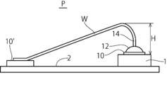
- a bonded portion formed on the electrode by crimping the melted FAB to the electrode 10 as shown in FIG. 1 (hereinafter, this bonded portion is referred to as a “1st bond portion”).
- the strength at the boundary portion 14 between the wire 12 and the wire W (hereinafter, this boundary portion may be referred to as “1st neck portion”) 14 can be improved.
- the strength at the 1st neck portion 14 can be improved, so the thermal shock resistance is improved. Can be good.
- Pd and Cu can improve the normal temperature tensile strength and the strength of the 1st neck portion 14 with any element. Therefore, even when it does not contain any one element of Pd and Cu, or even when the content of one element is less than a predetermined amount, the room temperature tensile strength and the 1st neck portion 14 can be obtained by adding the other element. The strength of can be improved.
- the content of Pd can be 0.1% by mass or more and 10% by mass or less.
- the Cu content can be 0.05 mass% or more and 2 mass% or less.
- the bonding wire can improve the heat resistance of the wire.
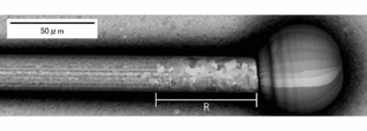
- a large region R of crystal grains called HAZ is generated in the wire portion immediately adjacent to the FAB due to heat at the time of FAB formation (see FIG. 2).
- a bonding wire made of high-purity Ag has low heat resistance and is easily affected by heat, and therefore has a long HAZ. Therefore, the bonding wire made of high-purity Ag has a large loop height H when the electrodes 10 and 10 'are connected (see FIG. 1). When the loop height H increases, the semiconductor device cannot be thinned and the loop shape tends to become abnormal.
- first additive element group one or more elements selected from the group consisting of Ca, Y, Sm, La, Ce, Nd, Eu, Gd, and Sc (hereinafter sometimes referred to as “first additive element group”)
- the first additive element group In a bonding wire mainly composed of Ag, when the Pd content is 0.1% by mass or more and 10% by mass or less and the Cu content is 0.05% by mass or more and 2% by mass or less, the first additive element group
- the total content of can be 20 mass ppm or more and 500 mass ppm or less.
- the total content of the first additive element group is 20 mass ppm or more, the heat resistance is improved and the length of the HAZ generated during FAB formation is shortened, so the loop height H at the time of connection is reduced. Can do.
- the total content of the first additive element group is 500 ppm by mass or less, a FAB having a high sphericity is easily obtained.
- first element in addition to the above-described Pd, Cu, and first additive element group, one or more elements selected from the group consisting of Ge, Bi, and Mg (hereinafter referred to as “first element”). It may also be added additionally. That is, the second additive element group is an optional component. If the total content of the second additive element group is 500 ppm by mass or less, the above-described operational effects due to the addition of Pd, Cu, and the first additive element group are not impaired. Further, if the total content of the second additive element group is 20 mass ppm or more, the heat resistance of the wire is improved, and HAZ is less likely to occur during FAB formation, and the height of the loop during connection may be reduced. it can. Therefore, when adding a 2nd additive element group, it is preferable that the sum total of content of a 2nd additive element group is 20 mass ppm or more and 500 mass ppm or less.
- Ag having a purity of 99.9% by mass or more, a Pd content of 0.1% by mass to 10% by mass, a Cu content of 0.05% by mass to 2% by mass, a first additive element group
- An Ag alloy to which Pd, Cu, and the first additive element group have been added so as to have a total content of 20 ppm to 500 ppm in mass is prepared.
- the total content of the second additive element group in addition to Pd, Cu and the first additive element group is 20 mass ppm or more and 500 mass ppm or less.
- the second additive element group is also added to produce an Ag alloy.
- the obtained Ag alloy is cast into a rod-shaped ingot having a predetermined diameter by a continuous casting method.
- the rod-shaped ingot is drawn to reduce the diameter until it reaches a predetermined diameter to obtain a bonding wire.
- a tempering heat treatment is performed by running in a heat treatment furnace as necessary to obtain a bonding wire.
- the bonding wire of the present embodiment has a Pd content of 0.1% by mass to 10% by mass, a Cu content of 0.05% by mass to 2% by mass, Ca, Y, Sm, La, Ce,
- the total content of one or more elements selected from the group consisting of Nd, Eu, Gd, and Sc is 20 mass ppm or more and 500 mass ppm or less, and the balance is made of Ag.
- the height of the loop that can be formed at the time of connection can be reduced, and the semiconductor device can be made thinner.
- the bonding wire of this embodiment when the total of the Pd content C Pd and the Cu content C Cu (C Pd + C Cu ) is 10.05% by mass or less, the light reflectance of the bonding wire is reduced. Can be suppressed. Therefore, when the bonding wire is used for connecting a light emitting element such as an LED, a light emitting element with high luminous efficiency can be obtained.
- the bonding wire of this embodiment you may contain the 1 type (s) or 2 or more types of element selected from the group which consists of Ge, Bi, and Mg, and the sum total of content of these elements is 20 mass ppm. The amount is preferably 500 ppm by mass or less.
- a loop formed at the time of connection by additionally containing one or more elements selected from the group consisting of Ge, Bi, and Mg
- the semiconductor device can be thinned.
- an Ag raw material having a purity of 99.9% by mass or more an Ag alloy having a composition as shown in Table 1 below was dissolved, and a rod-shaped ingot was produced by a continuous casting method.
- the produced rod-shaped ingot was drawn to reduce the diameter until reaching a diameter of 25 ⁇ m, and then subjected to a tempering heat treatment to obtain bonding wires of Examples 1 to 10 and Comparative Examples 1 to 7.
- the wire diameters (diameters) of the bonding wires in Examples 1 to 10 and Comparative Examples 1 to 7 are all 25 ⁇ m.
- the appearance was observed, and the lengths of the fabricated FAB in the wire parallel direction and the vertical direction were measured.
- the ratio (X / Y) of the length X of the FAB in the wire parallel direction to the length Y in the vertical direction is used as an index of true sphericity.
- the number of FABs judged to be spherical was counted.
- the results show the ratio of the number of FABs judged to have true sphericity to the 500 FABs produced.
- (4) Length of HAZ The appearance of the wire from which the FAB was produced in the above (3) was observed with the above-mentioned general-purpose electron microscope, the length of the HAZ generated in the wire portion closest to the FAB was measured, and the average value was calculated.
- the results are as shown in Table 2.
- the normal temperature tensile strength is 10.0 gf or more
- the 1st neck portion strength is 10.5 gf or more
- the HAZ length is 150 ⁇ m or less
- the FAB sphericity is 100. %
- the thermal cycle test was “A”, and the light reflectance was 90% or more, and good results were obtained for all the evaluation items.
- Comparative Example 4 the Cu content is less than 0.05% by mass, but since the Pd content is larger than that in Comparative Example 3, the room temperature tensile strength and the strength of the 1st neck portion are high, and good results are obtained. It was. However, in Comparative Example 4, FAB sphericity deteriorated. Further, in Comparative Example 4, the evaluation of the thermal cycle test was “D” because the adhesion between the 1st bond and the electrode was deteriorated as the FAB sphericity deteriorated. That is, in Comparative Example 4, since the Cu content was less than 0.05% by mass, it was impossible to achieve both normal temperature tensile strength, 1st neck portion strength, and FAB sphericity.
- Comparative Example 6 since the Pd content exceeds 10% by mass, the light reflectivity was lowered. In Comparative Example 6, since the total content of one or more elements selected from the group consisting of Ge, Bi, and Mg exceeds 500 ppm by mass, FAB sphericity deteriorates, The evaluation of the cycle test was “D”.
- Comparative Example 7 since the Pd content exceeded 10% by mass, the light reflectance was lowered. In Comparative Example 7, the total content of one or more elements selected from the group consisting of Ca, Y, Sm, La, Ce, Nd, Eu, Gd, and Sc is 500 mass ppm. Therefore, the FAB sphericity deteriorated.
Landscapes
- Chemical & Material Sciences (AREA)
- Engineering & Computer Science (AREA)
- Materials Engineering (AREA)
- Mechanical Engineering (AREA)
- Metallurgy (AREA)
- Organic Chemistry (AREA)
- Wire Bonding (AREA)
- Powder Metallurgy (AREA)
- Internal Circuitry In Semiconductor Integrated Circuit Devices (AREA)
Abstract
FABの真球性や耐熱衝撃性を良好にすることができるとともに、結線時にできるループの高さを小さく設けることができ半導体装置の薄型化が可能となるAgを主成分とするボンディングワイヤ及び半導体装置を提供することを目的とする。
Pdの含有量が0.1質量%以上10質量%以下、Cuの含有量が0.05質量%以上2質量%以下、Ca、Y、Sm、La、Ce、Nd、Eu、Gd、及びScからなる群から選択された1種又は2種以上の元素の含有量の合計が20質量ppm以上500質量ppm以下、Ge、Bi、及びMgからなる群から選択された1種又は2種以上の元素の含有量の合計が0質量ppm以上500質量ppm以下であり、残部がAgからなるものとする。
Description
本発明は、Ag(銀)を主成分とするボンディングワイヤ及び半導体装置に関する。
半導体素子上の電極と基板の電極との結線に用いられるボンディングワイヤは、一般に非常に細いため、導電性が良好で加工性に優れた金属材料により製造されている。特に、化学的な安定性や大気中での取り扱いやすさから、従来からAu(金)を主成分とするボンディングワイヤが広く用いられている。しかし、従来のAuを主成分とするボンディングワイヤは質量の99%以上がAuであり非常に高価である。そこで、Auに比べて安価なAgを主成分とするボンディングワイヤが提案されている(例えば、下記特許文献1)。
上記特許文献1のボンディングワイヤでは、放電加熱等によりボンディングワイヤの先端に形成されるフリーエアボール(以下、「FAB」と記載することもある)の真球性や耐熱性を良好にするため、Pd(パラジウム)、Au、Ca(カルシウム)、Ge(ゲルマニウム)、Bi(ビスマス)、Mg(マグネシウム)、Cu(銅)などの元素が主成分のAgに添加されている。
近年、半導体装置では、より過酷な熱環境における使用や薄型化に対する要求が高い。これに伴い、Agを主成分とするボンディングワイヤでは、周囲温度の変化に対する耐性(耐熱衝撃性)や、電極間を結線した時にできるループの高さを小さくすることが求められている。しかし、上記特許文献1のボンディングワイヤでは、これらの要求を充分に満足できない場合がある。
本発明は、上記事情に鑑みてなされたものであり、Agを主成分とするボンディングワイヤ及び半導体装置において、FABの真球性や耐熱衝撃性を良好にするとともに、結線時にできるループの高さを小さく設けることができ半導体装置の薄型化を可能とすることを目的とする。
上記課題を解決するため、本発明のボンディングワイヤは、Pdの含有量が0.1質量%以上10質量%以下、Cuの含有量が0.05質量%以上2質量%以下、Ca、Y、Sm、La、Ce、Nd、Eu、Gd、及びScからなる群から選択された1種又は2種以上の元素の含有量の合計が20質量ppm以上500質量ppm以下、Ge、Bi、及びMgからなる群から選択された1種又は2種以上の元素の含有量の合計が0質量ppm以上500質量ppm以下であり、残部がAgからなるものである。
本発明に係るボンディングワイヤにおいて、Cuの含有量CCuに対するPdの含有量CPdの比率(CPd/CCu)が2以上とすることができる。
本発明に係るボンディングワイヤにおいて、Cuの含有量CCuとPdの含有量CPdの合計が10.05質量%以下とすることができる。
本発明に係るボンディングワイヤのGe、Bi、及びMgからなる群から選択された1種又は2種以上の元素の含有量の合計は0質量ppmとすることができる。
また、本発明に係るボンディングのGe、Bi、及びMgからなる群から選択された1種又は2種以上の元素の含有量の合計は20質量ppm以上500質量ppm以下とすることができる。
本発明の半導体装置は、上記の本発明のいずれか1つに係るボンディングワイヤを使用した半導体装置である。
本発明のAgを主成分とするボンディングワイヤでは、FABの真球性や耐熱衝撃性を良好にすることができるとともに、結線時にできるループの高さを小さく設けることができ半導体装置の薄型化が可能となる。
以下、本発明の一実施形態に係るボンディングワイヤWについて図面を参照して説明する。
本実施形態のボンディングワイヤWは、図1に例示するように、半導体装置(パワーIC、LSI、トランジスタ、BGA(Ball Grid Array package)、QFN(Quad Flat Nonlead package)、LED(発光ダイオード)等)における半導体素子1上の電極(例えば、Al合金電極、ニッケル・パラジウム・金被覆電極、Au被覆電極等)10と、回路配線基板(リードフレーム、セラミック基板、プリント基板等)2の導体配線(電極)10‘とをボールボンディング法によって接続するためのボンディングワイヤである。なお、本実施形態のボンディングワイヤWは、半導体装置以外にも種々の態様のボンディングワイヤとして使用することができる。
このボンディングワイヤWは、0.1質量%以上10質量%以下のPdと、0.05質量%以上2質量%以下のCuと、20質量ppm以上500質量ppm以下のCa、Y、Sm、La、Ce、Nd、Eu、Gd、及びScからなる群から選択された1種又は2種以上の元素とを含有し、残部がAgからなるものである。
ボンディングワイヤWの線径は用途に応じて種々の大きさとしてよい。例えば、ボンディングワイヤWの線径は5μm以上150μm以下とすることができる。
具体的には、ボンディングワイヤWを構成するAgは、精製上不可避的に存在する不純物、例えば、Pd、Bi(ビスマス)、Cu(銅)、Fe(鉄)等を含有してもよく、純度99.9質量%以上のAgを用いてボンディングワイヤWを構成するAg合金を製作することが好ましい。
Pd及びCuを含有することにより、ワイヤWの常温での引張強度(以下、この引張強度を「常温引張強度」ということもある)を向上させることができる。常温引張強度が向上することで、ワイヤボンディング後の樹脂封止の際に流入してきた樹脂によるワイヤループの変形(いわゆる、ワイヤフロー)が発生しにくくなる。
また、Pd及びCuを含有することにより、図1に示すような電極10に溶融したFABを圧着することで電極上に形成された接合部(以下、この接合部を「1stボンド部」ということもある)12とワイヤWとの境界部分(以下、この境界部分を「1stネック部」ということもある)14における強度を向上させることができる。ボンディングワイヤが周囲温度の変化により断線する場合、その多くが1stネック部14で破断するが、Pd及びCuを含有することにより1stネック部14における強度を向上させることができるため、耐熱衝撃性を良好にすることができる。
Pd及びCuは、いずれの元素も常温引張強度及び1stネック部14の強度を向上させることができる。そのため、Pd及びCuのいずれか一方の元素を含有しない場合や、一方の元素の含有量が所定量より少ない場合であっても、他方の元素を添加することで常温引張強度及び1stネック部14の強度を向上させることができる。
しかし、Pd及びCuのいずれか一方の元素を含有しない場合、あるいは、一方の元素の含有量が所定量より少ない場合、一方の元素を所定量以上含有する場合に比べて、Ag以外の元素の添加によってFABの真球性が悪化しやすくなる。言い換えれば、Pdを少なくとも0.1質量%以上、Cuを少なくとも0.05質量%以上、それぞれ含有することで、Ag以外の添加元素の含有量が増えてもFABの真球性が悪化しにくくなり、真球度の高いFABが得やすくなる。
一方、Pdの含有量が10質量%を越えると、固有抵抗値が大きくなってIC用途の場合に半導体装置が過熱するような不具合が出たり、LED用途の場合にボンディングワイヤの光線反射率が低下する。また、Cuの含有量が2質量%を超えるとFABの真球性が悪化する。
よって、Pdの含有量は0.1質量%以上10質量%以下とすることができる。Cuの含有量は0.05質量%以上2質量%以下とすることができる。このような範囲内にPd及びCuの含有量を設定することで、FABの形成性を良好に保ちつつ、常温引張強度及び1stネック部14の強度を向上させてワイヤフローの抑制及び耐熱衝撃性の向上を図ることができる。特に、真球度の高いFABが安定して得られることから、Cuの含有量CCuに対するPdの含有量CPdの比率(CPd/CCu)が2以上になるように、Pd及びCuを含有することが好ましい。また、ボンディングワイヤの光線反射率の低下を抑えることができるため、Pdの含有量CPdとCuの含有量CCuの合計(CPd+CCu)が10.05質量%以下であることが好ましい。
Ca、Y、Sm、La、Ce、Nd、Eu、Gd、及びScは、ワイヤの耐熱性を向上させることができる。ボンディングワイヤは、FAB形成時の熱によってFAB直近のワイヤ部分にHAZと呼ばれる結晶粒の大きな領域Rが発生する(図2参照)。高純度のAgからなるボンディングワイヤは、耐熱性が低く熱の影響を受けやすいため、HAZが長くなる。そのため、高純度のAgからなるボンディングワイヤは、電極10,10‘を結線した時にできるループ高さHが大きくなる(図1参照)。ループ高さHが大きくなると、半導体装置を薄型化できなくなるとともに、ループ形状が異常となりやすい。
しかし、Ca、Y、Sm、La、Ce、Nd、Eu、Gd、及びScからなる群から選択された1種又は2種以上の元素(以下、「第1添加元素群」ということもある)を含有することにより、耐熱性が向上するとともにFAB形成時に発生するHAZの長さが短くなるため、結線時のループ高さHを小さくすることができる。
Agを主成分とするボンディングワイヤにおいて、Pdの含有量が0.1質量%以上10質量%以下で、Cuの含有量が0.05質量%以上2質量%以下の場合、第1添加元素群の含有量の合計が20質量ppm以上500質量ppm以下とすることができる。
第1添加元素群の含有量の合計が20質量ppm以上であると、耐熱性が向上するとともにFAB形成時に発生するHAZの長さが短くなるため、結線時のループ高さHを小さくすることができる。第1添加元素群の含有量の合計が500質量ppm以下であると真球度の高いFABが得やすくなる。
なお、本発明では、上記したPd、Cu、及び第1添加元素群に加えて、更に、Ge、Bi、及びMgからなる群から選択された1種又は2種以上の元素(以下、「第2添加元素群」ということもある)を追加的に添加してもよい。つまり、第2添加元素群は任意成分である。この第2添加元素群の含有量の合計が500質量ppm以下であれば、Pd、Cu、及び第1添加元素群を添加したことによる上記した作用効果を損なうことがない。また、第2添加元素群の含有量の合計が20質量ppm以上であると、ワイヤの耐熱性が向上するとともにFAB形成時にHAZが発生しにくくなり結線時のループの高さを小さくすることができる。よって、第2添加元素群を添加する場合、第2添加元素群の含有量の合計は、20質量ppm以上500質量ppm以下であることが好ましい。
次に、このような構成のボンディングワイヤの製造方法の一例を説明する。
まず、純度99.9質量%以上のAgに、Pdの含有量が0.1質量%以上10質量%以下、Cuの含有量が0.05質量%以上2質量%以下、第1添加元素群の含有量の合計が20質量ppm以上500質量ppm以下となるようにPdとCuと第1添加元素群を添加したAg合金を作製する。なお、第2添加元素群を含有するボンディングワイヤを製造する場合は、PdとCuと第1添加元素群に加えて、第2添加元素群の含有量の合計が20質量ppm以上500質量ppm以下となるように第2添加元素群も添加してAg合金を作製する。得られたAg合金は、連続鋳造法にて所定の直径の棒状インゴットに鋳造される。
次いで、棒状インゴットを伸線加工して所定の直径に達するまで縮径してボンディングワイヤとする。なお、必要に応じて伸線加工の途中で軟化熱処理を行っても良い。
そして、所定の直径まで伸線加工を行った後、必要に応じて熱処理炉中を走行させて調質熱処理を行い、ボンディングワイヤが得られる。
本実施形態のボンディングワイヤは、Pdの含有量が0.1質量%以上10質量%以下、Cuの含有量が0.05質量%以上2質量%以下、Ca、Y、Sm、La、Ce、Nd、Eu、Gd、及びScからなる群から選択された1種又は2種以上の元素の含有量の合計が20質量ppm以上500質量ppm以下であり、残部がAgからなるので、FABの真球性や耐熱衝撃性を良好にするとともに、結線時にできるループの高さを小さく設けることができ半導体装置の薄型化を可能とすることができる。
本実施形態のボンディングワイヤにおいて、Cuの含有量CCuに対するPdの含有量CPdの比率(CPd/CCu)が2以上になるように、Pd及びCuの含有量を設定することで、真球度の高いFABを安定して得ることができる。
また、本実施形態のボンディングワイヤにおいて、Pdの含有量CPdとCuの含有量CCuの合計(CPd+CCu)が10.05質量%以下であると、ボンディングワイヤの光線反射率の低下を抑えることができる。そのため、当該ボンディングワイヤをLED等の発光素子の結線に用いると高い発光効率の発光素子を得ることができる。
また、本実施形態のボンディングワイヤにおいて、Ge、Bi、及びMgからなる群から選択された1種又は2種以上の元素を含有してもよく、これらの元素の含有量の合計は20質量ppm以上500質量ppm以下であることが好ましい。Pd、Cu、及び第1添加元素群に加えて、更に、Ge、Bi、及びMgからなる群から選択された1種又は2種以上の元素を追加的に含有することで、結線時にできるループの高さを小さく設けることができ半導体装置の薄型化が可能となる。
以上、本発明の実施形態を説明したが、これらの実施形態は例として提示したものであり、発明の範囲を限定することを意図していない。これらの実施形態は、その他の様々な形態で実施されることが可能であり、発明の趣旨を逸脱しない範囲で、種々の省略、置き換え、変更を行うことができる。これらの実施形態やその変形は、発明の範囲や要旨に含まれると同様に、特許請求の範囲に記載された発明とその均等の範囲に含まれるものである。
以下、本発明を実施例によって更に具体的に説明するが、本発明はこれら実施例に限定されるものではない。
純度99.9質量%以上のAg原料を用いて、下記表1に示すような組成のAg合金を溶解し、連続鋳造法にて棒状インゴットを作製した。作製した棒状インゴットに対して伸線加工を施して直径25μmに達するまで縮径し、その後、調質熱処理を施し、実施例1~10及び比較例1~7のボンディングワイヤを得た。なお、実施例1~10及び比較例1~7のボンディングワイヤの線径(直径)はいずれも25μmである。
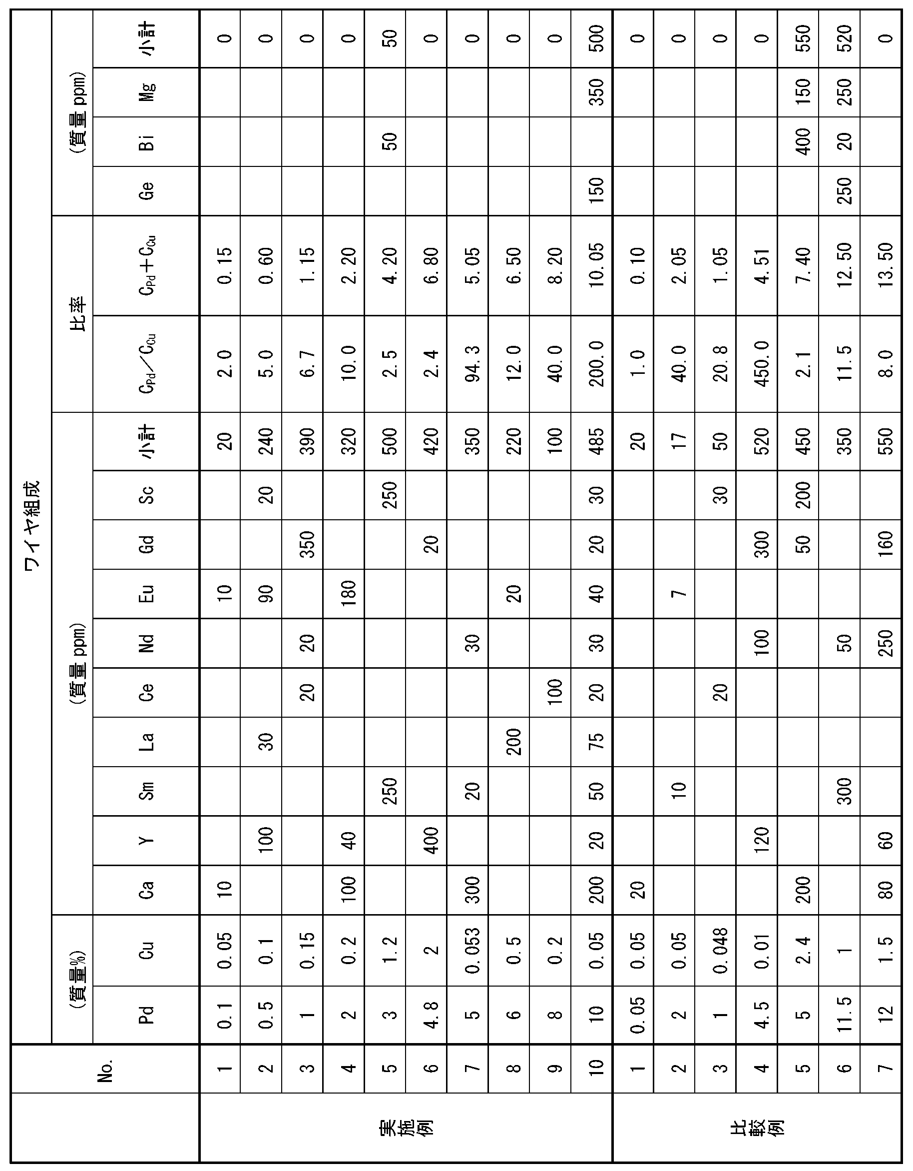
得られた実施例1~10及び比較例1~7のボンディングワイヤにつき、(1)常温引張強度、(2)1stネック部の強度、(3)FAB真球性、(4)FAB形成時の熱によってFAB直近のワイヤ部分に生じたHAZの長さ、(5)熱サイクル試験、及び(6)光線反射率について評価を行った。具体的な評価方法は以下のとおりである。
(1)常温引張強度
15~25℃の室温(常温)中で長さ100mmのワイヤを破断するまで引っ張り、破断した時の荷重を測定した。
(2)1stネック部の強度
図1に示すように電極間をボンディングワイヤで結線した後、ピール試験機によって、1stネック部14からワイヤWが破断するまで1stボンド12を引き離す方向へワイヤWを引っ張り、ワイヤWが1stネック部14から破断した時の荷重を測定した。
(3)FAB真球性
実施例1~10及び比較例1~7のボンディングワイヤに対して、ワイヤボンダー(K&S社製、IConn)にてワイヤ直径の2.0倍の大きさのFABを窒素ガス雰囲気で作製した。FAB形成性の評価としては、実施例1~10及び比較例1~7のボンディングワイヤ毎にFABを500個ずつ作製した後、汎用型電子顕微鏡(日本電子(株)製、JSM-6510LA)にて外観観察を行い、作製したFABのワイヤ平行方向と垂直方向の長さをそれぞれ測定した。FABのワイヤ平行方向の長さXと垂直方向の長さYの比(X/Y)を真球性の指標として、95%~100%であれば「真球性有り」と判断し、真球性有りと判断したFABの個数をカウントした。結果は、作製した500個のFABに対する真球性有りと判断したFABの個数の比率を示す。
(4)HAZの長さ
上記(3)においてFABを作製したワイヤを上記汎用型電子顕微鏡にて外観観察を行い、FAB直近のワイヤ部分に発生したHAZの長さを測定し、その平均値を算出した。
(5)熱サイクル試験
電極間をボンディングワイヤで結線した後、シリコーン樹脂封止をした半導体試料を市販の熱サイクル試験装置を用いて評価した。温度履歴は-40℃で60分間保持した後、125℃まで昇温しこの温度で60分間保持する。これを1サイクルとして、1000サイクルの試験を行った。試験後に電気的測定を行い、導通評価をした。評価したワイヤ数は500本であり、不良率が1%以下の場合は「A」、1%を超える場合は耐性が低いことから「D」とした。
(6)光線反射率
同種のLEDに実施例1~10、比較例1~7及び純銀のボンディングワイヤを結線し、樹脂封止をして各実施例、比較例及び純銀のボンディングワイヤによって結線したLED素子を作製した。作製した素子をJIS C8152に規定の方法により全光束測定を行った。測定結果は、純銀のワイヤで結線したLEDの光量を100%としたときの各実施例、比較例の光量を百分率に換算して示した。
(1)常温引張強度
15~25℃の室温(常温)中で長さ100mmのワイヤを破断するまで引っ張り、破断した時の荷重を測定した。
(2)1stネック部の強度
図1に示すように電極間をボンディングワイヤで結線した後、ピール試験機によって、1stネック部14からワイヤWが破断するまで1stボンド12を引き離す方向へワイヤWを引っ張り、ワイヤWが1stネック部14から破断した時の荷重を測定した。
(3)FAB真球性
実施例1~10及び比較例1~7のボンディングワイヤに対して、ワイヤボンダー(K&S社製、IConn)にてワイヤ直径の2.0倍の大きさのFABを窒素ガス雰囲気で作製した。FAB形成性の評価としては、実施例1~10及び比較例1~7のボンディングワイヤ毎にFABを500個ずつ作製した後、汎用型電子顕微鏡(日本電子(株)製、JSM-6510LA)にて外観観察を行い、作製したFABのワイヤ平行方向と垂直方向の長さをそれぞれ測定した。FABのワイヤ平行方向の長さXと垂直方向の長さYの比(X/Y)を真球性の指標として、95%~100%であれば「真球性有り」と判断し、真球性有りと判断したFABの個数をカウントした。結果は、作製した500個のFABに対する真球性有りと判断したFABの個数の比率を示す。
(4)HAZの長さ
上記(3)においてFABを作製したワイヤを上記汎用型電子顕微鏡にて外観観察を行い、FAB直近のワイヤ部分に発生したHAZの長さを測定し、その平均値を算出した。
(5)熱サイクル試験
電極間をボンディングワイヤで結線した後、シリコーン樹脂封止をした半導体試料を市販の熱サイクル試験装置を用いて評価した。温度履歴は-40℃で60分間保持した後、125℃まで昇温しこの温度で60分間保持する。これを1サイクルとして、1000サイクルの試験を行った。試験後に電気的測定を行い、導通評価をした。評価したワイヤ数は500本であり、不良率が1%以下の場合は「A」、1%を超える場合は耐性が低いことから「D」とした。
(6)光線反射率
同種のLEDに実施例1~10、比較例1~7及び純銀のボンディングワイヤを結線し、樹脂封止をして各実施例、比較例及び純銀のボンディングワイヤによって結線したLED素子を作製した。作製した素子をJIS C8152に規定の方法により全光束測定を行った。測定結果は、純銀のワイヤで結線したLEDの光量を100%としたときの各実施例、比較例の光量を百分率に換算して示した。
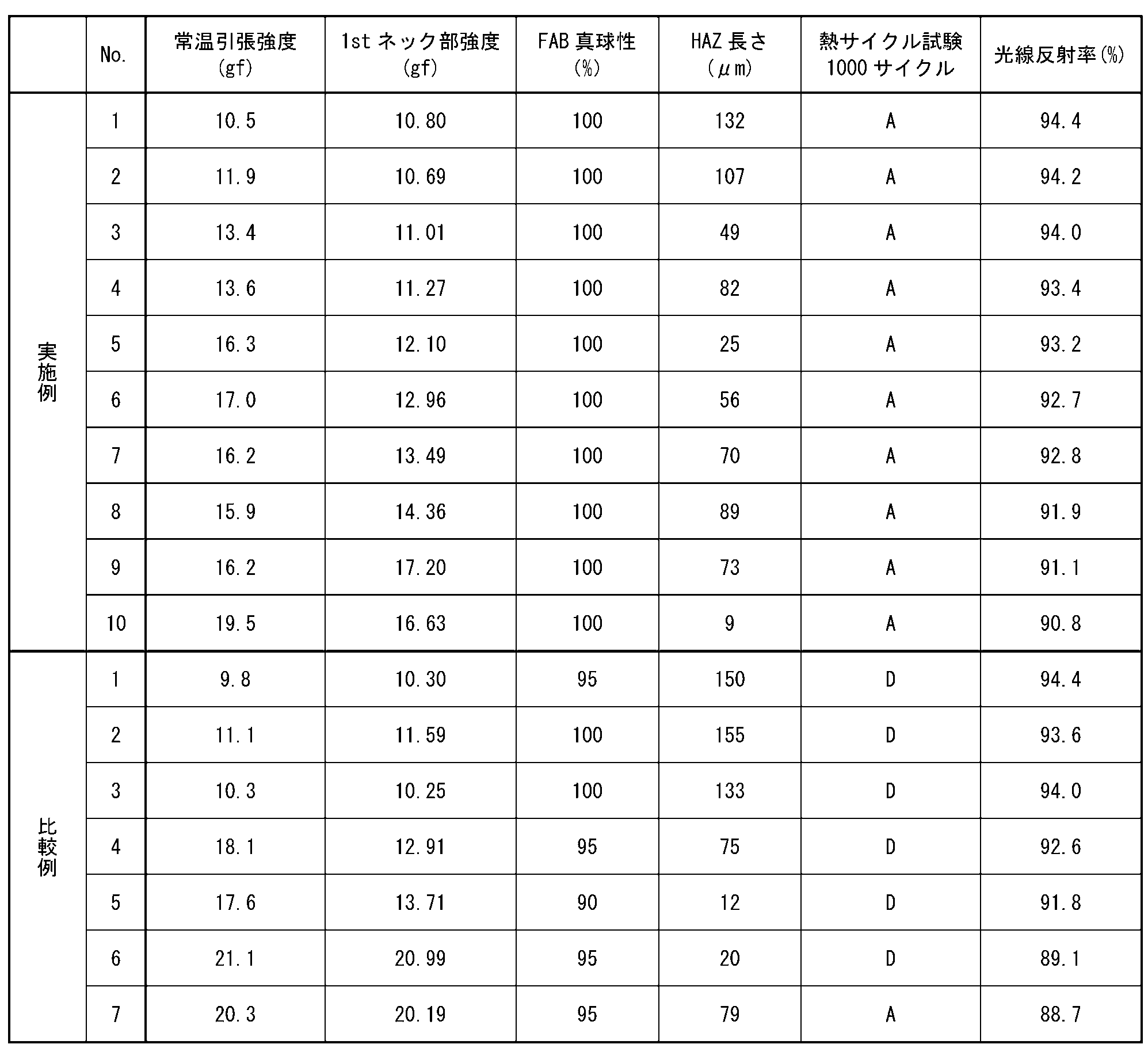
結果は、表2に示すとおりであり、実施例1~10では、常温引張強度が10.0gf以上、1stネック部の強度が10.5gf以上、HAZ長さ150μm以下、FAB真球性が100%、熱サイクル試験が「A」、光線反射率が90%以上となり、いずれの評価項目も良好な結果が得られた。
比較例1では、Pdの含有量が0.1質量%未満であるため、常温引張強度及び1stネック部の強度が低く、熱サイクル試験の評価が「D」となった。
比較例2では、Ca、Y、Sm、La、Ce、Nd、Eu、Gd、及びScからなる群から選択された1種又は2種以上の元素の含有量の合計が20質量ppm未満であるため、耐熱性が低く熱サイクル試験の評価が「D」となった。
比較例3では、Cuの含有量が0.05質量%未満であるため、1stネック部の強度が低く、熱サイクル試験の評価が「D」となった。
比較例4では、Cuの含有量が0.05質量%未満であるが、Pdの含有量が比較例3に比べて多いため常温引張強度及び1stネック部の強度が高く良好な結果が得られた。しかし、比較例4ではFAB真球性が悪化した。また、比較例4では、FAB真球性の悪化に伴い、1stボンドと電極との接着性が悪化するため熱サイクル試験の評価が「D」となった。つまり、比較例4では、Cuの含有量が0.05質量%未満であるため、常温引張強度及び1stネック部の強度とFAB真球性とを両立させることができなかった。
比較例5では、Cuの含有量が2質量%を越えるため、FAB真球性が悪化し、熱サイクル試験の評価が「D」となった。
比較例6では、Pdの含有量が10質量%を越えるため、光線反射率が低下した。また、比較例6では、Ge、Bi、及びMgからなる群から選択された1種又は2種以上の元素の含有量の合計が500質量ppmを越えるため、FAB真球性が悪化し、熱サイクル試験の評価が「D」となった。
比較例7では、Pdの含有量が10質量%を越えるため、光線反射率が低下した。また、比較例7では、Ca、Y、Sm、La、Ce、Nd、Eu、Gd、及びScからなる群から選択された1種又は2種以上の元素の含有量の合計が500質量ppmを越えるため、FAB真球性が悪化した。
Claims (6)
- Pdの含有量が0.1質量%以上10質量%以下、
Cuの含有量が0.05質量%以上2質量%以下、
Ca、Y、Sm、La、Ce、Nd、Eu、Gd、及びScからなる群から選択された1種又は2種以上の元素の含有量の合計が20質量ppm以上500質量ppm以下、
Ge、Bi、及びMgからなる群から選択された1種又は2種以上の元素の含有量の合計が0質量ppm以上500質量ppm以下であり、
残部がAgからなるボンディングワイヤ。 - Cuの含有量CCuに対するPdの含有量CPdの比率(CPd/CCu)が2以上である請求項1に記載のボンディングワイヤ。
- Cuの含有量CCuとPdの含有量CPdの合計が10.05質量%以下である請求項1又は2に記載のボンディングワイヤ。
- Ge、Bi、及びMgからなる群から選択された1種又は2種以上の元素の含有量の合計が0質量ppmである請求項1~3のいずれか1項に記載のボンディングワイヤ。
- Ge、Bi、及びMgからなる群から選択された1種又は2種以上の元素の含有量の合計が20質量ppm以上500質量ppm以下である請求項1~3のいずれか1項に記載のボンディングワイヤ。
- 請求項1~5のいずれか1項に記載のボンディングワイヤを使用した半導体装置。
Priority Applications (1)
| Application Number | Priority Date | Filing Date | Title |
|---|---|---|---|
| JP2019509050A JP6714150B2 (ja) | 2017-03-31 | 2018-03-02 | ボンディングワイヤ及び半導体装置 |
Applications Claiming Priority (2)
| Application Number | Priority Date | Filing Date | Title |
|---|---|---|---|
| JP2017-072394 | 2017-03-31 | ||
| JP2017072394 | 2017-03-31 |
Publications (1)
| Publication Number | Publication Date |
|---|---|
| WO2018180189A1 true WO2018180189A1 (ja) | 2018-10-04 |
Family
ID=63675539
Family Applications (1)
| Application Number | Title | Priority Date | Filing Date |
|---|---|---|---|
| PCT/JP2018/007938 Ceased WO2018180189A1 (ja) | 2017-03-31 | 2018-03-02 | ボンディングワイヤ及び半導体装置 |
Country Status (3)
| Country | Link |
|---|---|
| JP (1) | JP6714150B2 (ja) |
| TW (1) | TWI802555B (ja) |
| WO (1) | WO2018180189A1 (ja) |
Cited By (1)
| Publication number | Priority date | Publication date | Assignee | Title |
|---|---|---|---|---|
| CN113518687A (zh) * | 2019-04-26 | 2021-10-19 | 贺利氏材料新加坡有限公司 | 经涂覆线材 |
Citations (2)
| Publication number | Priority date | Publication date | Assignee | Title |
|---|---|---|---|---|
| JP2013048169A (ja) * | 2011-08-29 | 2013-03-07 | Tatsuta Electric Wire & Cable Co Ltd | ボールボンディング用ワイヤ |
| WO2015115241A1 (ja) * | 2014-01-31 | 2015-08-06 | タツタ電線株式会社 | ワイヤボンディング及びその製造方法 |
Family Cites Families (2)
| Publication number | Priority date | Publication date | Assignee | Title |
|---|---|---|---|---|
| JPH11288962A (ja) * | 1998-04-01 | 1999-10-19 | Sumitomo Metal Mining Co Ltd | ボンディングワイヤ |
| KR101513493B1 (ko) * | 2013-02-19 | 2015-04-20 | 엠케이전자 주식회사 | 은 합금 본딩 와이어 |
-
2017
- 2017-12-19 TW TW106144543A patent/TWI802555B/zh active
-
2018
- 2018-03-02 WO PCT/JP2018/007938 patent/WO2018180189A1/ja not_active Ceased
- 2018-03-02 JP JP2019509050A patent/JP6714150B2/ja active Active
Patent Citations (2)
| Publication number | Priority date | Publication date | Assignee | Title |
|---|---|---|---|---|
| JP2013048169A (ja) * | 2011-08-29 | 2013-03-07 | Tatsuta Electric Wire & Cable Co Ltd | ボールボンディング用ワイヤ |
| WO2015115241A1 (ja) * | 2014-01-31 | 2015-08-06 | タツタ電線株式会社 | ワイヤボンディング及びその製造方法 |
Cited By (2)
| Publication number | Priority date | Publication date | Assignee | Title |
|---|---|---|---|---|
| CN113518687A (zh) * | 2019-04-26 | 2021-10-19 | 贺利氏材料新加坡有限公司 | 经涂覆线材 |
| CN113518687B (zh) * | 2019-04-26 | 2023-03-10 | 贺利氏材料新加坡有限公司 | 经涂覆线材 |
Also Published As
| Publication number | Publication date |
|---|---|
| TWI802555B (zh) | 2023-05-21 |
| JPWO2018180189A1 (ja) | 2019-12-12 |
| TW201842201A (zh) | 2018-12-01 |
| JP6714150B2 (ja) | 2020-06-24 |
Similar Documents
| Publication | Publication Date | Title |
|---|---|---|
| JP5616165B2 (ja) | 銀ボンディングワイヤ | |
| CN104380446B (zh) | 焊接用线 | |
| JP5671512B2 (ja) | ボンディング用ワイヤ | |
| JP7573138B1 (ja) | ボンディングワイヤ | |
| JP7542583B2 (ja) | ボンディングワイヤ及び半導体装置 | |
| CN103842529B (zh) | 金(Au)合金键合线 | |
| CN100557784C (zh) | 接合引线用金合金线 | |
| JP6714150B2 (ja) | ボンディングワイヤ及び半導体装置 | |
| WO2017154453A1 (ja) | ボンディングワイヤ | |
| JP6103806B2 (ja) | ボールボンディング用ワイヤ | |
| CN111656501B (zh) | 接合线 | |
| TWI643274B (zh) | Copper alloy thin wire for ball bonding | |
| CN100550333C (zh) | 接合引线用金合金线 | |
| CN101238564A (zh) | 具有高初始接合性、高接合可靠性、压接球的高真圆性、高直进性、高耐树脂流动性及低电阻率的接合引线用金合金线 | |
| TWI391503B (zh) | Wire with gold alloy wire | |
| TW202548036A (zh) | 接合線 | |
| JP5339101B2 (ja) | バンプ用ワイヤ | |
| JPH1126491A (ja) | 半導体素子用金合金細線 | |
| JPS6329938A (ja) | 半導体装置 | |
| JP2008027951A (ja) | 半導体装置接続用金合金 |
Legal Events
| Date | Code | Title | Description |
|---|---|---|---|
| 121 | Ep: the epo has been informed by wipo that ep was designated in this application |
Ref document number: 18774273 Country of ref document: EP Kind code of ref document: A1 |
|
| ENP | Entry into the national phase |
Ref document number: 2019509050 Country of ref document: JP Kind code of ref document: A |
|
| NENP | Non-entry into the national phase |
Ref country code: DE |
|
| 122 | Ep: pct application non-entry in european phase |
Ref document number: 18774273 Country of ref document: EP Kind code of ref document: A1 |