WO2018179337A1 - ワイヤレス受電装置及びワイヤレス電力伝送システム - Google Patents
ワイヤレス受電装置及びワイヤレス電力伝送システム Download PDFInfo
- Publication number
- WO2018179337A1 WO2018179337A1 PCT/JP2017/013602 JP2017013602W WO2018179337A1 WO 2018179337 A1 WO2018179337 A1 WO 2018179337A1 JP 2017013602 W JP2017013602 W JP 2017013602W WO 2018179337 A1 WO2018179337 A1 WO 2018179337A1
- Authority
- WO
- WIPO (PCT)
- Prior art keywords
- voltage
- wireless power
- circuit
- power
- power transmission
- Prior art date
- Legal status (The legal status is an assumption and is not a legal conclusion. Google has not performed a legal analysis and makes no representation as to the accuracy of the status listed.)
- Ceased
Links
Images


Classifications
-
- H—ELECTRICITY
- H02—GENERATION; CONVERSION OR DISTRIBUTION OF ELECTRIC POWER
- H02J—ELECTRIC POWER NETWORKS; CIRCUIT ARRANGEMENTS OR SYSTEMS FOR SUPPLYING OR DISTRIBUTING ELECTRIC POWER; SYSTEMS FOR STORING ELECTRIC ENERGY
- H02J7/00—Circuit arrangements for charging or discharging batteries or for supplying loads from batteries
- H02J7/80—Circuit arrangements for charging or discharging batteries or for supplying loads from batteries including monitoring or indicating arrangements
- H02J7/82—Control of state of charge [SOC]
-
- H—ELECTRICITY
- H02—GENERATION; CONVERSION OR DISTRIBUTION OF ELECTRIC POWER
- H02J—ELECTRIC POWER NETWORKS; CIRCUIT ARRANGEMENTS OR SYSTEMS FOR SUPPLYING OR DISTRIBUTING ELECTRIC POWER; SYSTEMS FOR STORING ELECTRIC ENERGY
- H02J50/00—Circuit arrangements or systems for wireless supply or distribution of electric power
- H02J50/10—Circuit arrangements or systems for wireless supply or distribution of electric power using inductive coupling
-
- H—ELECTRICITY
- H02—GENERATION; CONVERSION OR DISTRIBUTION OF ELECTRIC POWER
- H02J—ELECTRIC POWER NETWORKS; CIRCUIT ARRANGEMENTS OR SYSTEMS FOR SUPPLYING OR DISTRIBUTING ELECTRIC POWER; SYSTEMS FOR STORING ELECTRIC ENERGY
- H02J50/00—Circuit arrangements or systems for wireless supply or distribution of electric power
- H02J50/80—Circuit arrangements or systems for wireless supply or distribution of electric power involving the exchange of data, concerning supply or distribution of electric power, between transmitting devices and receiving devices
-
- H—ELECTRICITY
- H02—GENERATION; CONVERSION OR DISTRIBUTION OF ELECTRIC POWER
- H02M—APPARATUS FOR CONVERSION BETWEEN AC AND AC, BETWEEN AC AND DC, OR BETWEEN DC AND DC, AND FOR USE WITH MAINS OR SIMILAR POWER SUPPLY SYSTEMS; CONVERSION OF DC OR AC INPUT POWER INTO SURGE OUTPUT POWER; CONTROL OR REGULATION THEREOF
- H02M3/00—Conversion of DC power input into DC power output
- H02M3/22—Conversion of DC power input into DC power output with intermediate conversion into AC
- H02M3/24—Conversion of DC power input into DC power output with intermediate conversion into AC by static converters
- H02M3/28—Conversion of DC power input into DC power output with intermediate conversion into AC by static converters using discharge tubes with control electrode or semiconductor devices with control electrode to produce the intermediate AC
-
- H—ELECTRICITY
- H02—GENERATION; CONVERSION OR DISTRIBUTION OF ELECTRIC POWER
- H02M—APPARATUS FOR CONVERSION BETWEEN AC AND AC, BETWEEN AC AND DC, OR BETWEEN DC AND DC, AND FOR USE WITH MAINS OR SIMILAR POWER SUPPLY SYSTEMS; CONVERSION OF DC OR AC INPUT POWER INTO SURGE OUTPUT POWER; CONTROL OR REGULATION THEREOF
- H02M7/00—Conversion of AC power input into DC power output; Conversion of DC power input into AC power output
- H02M7/02—Conversion of AC power input into DC power output without possibility of reversal
- H02M7/04—Conversion of AC power input into DC power output without possibility of reversal by static converters
- H02M7/12—Conversion of AC power input into DC power output without possibility of reversal by static converters using discharge tubes with control electrode or semiconductor devices with control electrode
- H02M7/21—Conversion of AC power input into DC power output without possibility of reversal by static converters using discharge tubes with control electrode or semiconductor devices with control electrode using devices of a triode or transistor type requiring continuous application of a control signal
- H02M7/217—Conversion of AC power input into DC power output without possibility of reversal by static converters using discharge tubes with control electrode or semiconductor devices with control electrode using devices of a triode or transistor type requiring continuous application of a control signal using semiconductor devices only
- H02M7/2176—Conversion of AC power input into DC power output without possibility of reversal by static converters using discharge tubes with control electrode or semiconductor devices with control electrode using devices of a triode or transistor type requiring continuous application of a control signal using semiconductor devices only comprising a passive stage to generate a rectified sinusoidal voltage and a controlled switching element in series between such stage and the output
-
- H—ELECTRICITY
- H02—GENERATION; CONVERSION OR DISTRIBUTION OF ELECTRIC POWER
- H02J—ELECTRIC POWER NETWORKS; CIRCUIT ARRANGEMENTS OR SYSTEMS FOR SUPPLYING OR DISTRIBUTING ELECTRIC POWER; SYSTEMS FOR STORING ELECTRIC ENERGY
- H02J50/00—Circuit arrangements or systems for wireless supply or distribution of electric power
- H02J50/10—Circuit arrangements or systems for wireless supply or distribution of electric power using inductive coupling
- H02J50/12—Circuit arrangements or systems for wireless supply or distribution of electric power using inductive coupling of the resonant type
Definitions
- the present invention relates to a wireless power receiving apparatus and a wireless power transmission system.
- a wireless power transmission system configured to perform power transmission using wireless power transmission technology.
- the wireless power transmission system is configured to include a wireless power transmitting device that transmits power and a wireless power receiving device that receives the power transmitted by the wireless power transmitting device.
- Wireless power transmission technology is used to charge a load (for example, a secondary battery) mounted on a smartphone or an electric vehicle, for example.
- the wireless power transmission device is a charger
- the wireless power reception device is mounted on a smartphone or an electric vehicle.
- a lithium ion battery is mainstream.
- Patent Document 1 discloses an example of a wireless power transmission system.
- a filter circuit is provided after the rectifier circuit in the wireless power receiving apparatus. This filter circuit plays a role of reducing the ripple voltage generated by the operation of the switching power supply in the wireless power transmission apparatus.
- the inventors of the present application are considering performing feedback control of a voltage applied to a load in a wireless power transmission system. Specifically, it is considered to control the output of the wireless power transmission device so that the voltage applied to the load is equal to the target voltage.
- one of the objects of the present invention is to provide a wireless power receiving apparatus and a wireless power transmission system that can favorably perform feedback control when a filter circuit is provided in front of a load.
- a wireless power receiving device is a wireless power receiving device that wirelessly receives power transmitted from a wireless power transmitting device, and includes a power receiving coil that takes in AC power through an AC magnetic field, and AC power received by the power receiving coil.
- a rectifier circuit that converts DC power into DC power and outputs it to a load, a filter circuit provided between the rectifier circuit and the load, an input voltage detection circuit that detects an input voltage of the filter circuit, and the filter circuit
- An output voltage detection circuit that detects an output voltage, and a target voltage that generates a second target voltage that is a target value of the input voltage based on the output voltage and a first target voltage that is a target value of the output voltage A generation circuit; and a power-receiving-side transmitter that transmits difference information indicating a difference between the input voltage and the second target voltage to the wireless power transmission device. It is a Iyaresu powered device.
- the second target voltage when the output voltage is lower than the first target voltage, the second target voltage is generated in the direction of increasing the input voltage, and when the output voltage is higher than the first target voltage, the input voltage is increased. It becomes possible to generate the second target voltage in the decreasing direction, and as a result, the output voltage can be converged to the first target voltage while the input voltage is targeted for feedback control. Therefore, it is possible to suitably perform feedback control when a filter circuit is provided in front of the load.
- the target voltage generation circuit includes a subtraction circuit that calculates a differential voltage between the input voltage and the output voltage, and the second target by adding the differential voltage to the first target voltage. And an adder circuit for generating a voltage. Accordingly, the second target voltage can be suitably generated by the target voltage generation circuit.
- the target voltage generation circuit includes a subtraction circuit that calculates a differential voltage between the output voltage and the first target voltage, and the second target by adding the differential voltage to the input voltage. And an adder circuit for generating a voltage. Also by this, the second target voltage can be suitably generated by the target voltage generation circuit.
- the power receiving side transmitter may transmit an error signal to the wireless power transmitting apparatus when the second target voltage exceeds a reference value. According to this, it becomes possible to detect a failure of the filter circuit.
- the wireless power receiving apparatus may further include a charge state detection circuit that determines a charge state of the load based on a change in the differential voltage. According to this, it becomes possible to grasp
- the input voltage detection circuit may detect the input voltage with an effective value
- the output voltage detection circuit may detect the output voltage with an effective value. According to this, since the influence of the ripple voltage on the input voltage and the output voltage can be reduced, the second target voltage can be generated with high accuracy.
- a wireless power transmission system is a wireless power transmission system that wirelessly transmits power from a wireless power transmission device to a wireless power reception device, and the wireless power transmission device converts an input DC power into an AC power. And a power transmission coil that receives the AC power from the power conversion circuit to generate an AC magnetic field, and a power transmission side transmitter that transmits information to and from the wireless power reception device.
- the power conversion circuit is a wireless device that controls AC power supplied to the power transmission coil based on the difference information transmitted from the power transmission side transmitter and received by the power transmission side transmitter. It is a power transmission system.
- the second target voltage when the output voltage is lower than the first target voltage, the second target voltage is generated in the direction of increasing the input voltage, and when the output voltage is higher than the first target voltage, the input voltage is increased. It becomes possible to generate the second target voltage in the decreasing direction. Then, the power conversion circuit performs output control of the power transmission coil so that the second target voltage thus generated and the input voltage are equal, whereby the output voltage can be converged to the first target voltage. Therefore, it is possible to suitably perform feedback control when a filter circuit is provided in front of the load.
- a wireless power transmission system is a wireless power transmission system that wirelessly transmits power from a wireless power transmission device to a wireless power reception device, wherein the wireless power transmission device converts input DC power to AC power.
- a power conversion circuit for conversion; a power transmission coil that receives the AC power from the power conversion circuit to generate an AC magnetic field; and a power transmission side transmitter that transmits information to and from the wireless power reception device, and the wireless power reception device Is provided between the rectifier circuit and the load, a power receiving coil that takes in AC power via an AC magnetic field, a rectifier circuit that converts AC power received by the power receiving coil into DC power, and outputs the DC power to a load.
- a filter circuit ; an input voltage detection circuit for detecting an input voltage of the filter circuit; and an output voltage of the filter circuit. And an output voltage detection circuit that transmits the input voltage and the output voltage to the wireless power transmission device, wherein the wireless power transmission device has a first value that is the output voltage and a target value of the output voltage.
- a target voltage generation circuit that generates a second target voltage that is a target value of the input voltage based on a target voltage of 1; and the power conversion circuit includes: the input voltage and the second target voltage;
- the wireless power transmission system controls AC power supplied to the power transmission coil based on difference information indicating a difference.
- the second target voltage when the output voltage is smaller than the first target voltage, the second target voltage is generated in the direction of increasing the input voltage, and when the output voltage is larger than the first target voltage, the input voltage is decreased. It becomes possible to generate the second target voltage in the direction. Then, the power conversion circuit performs output control of the power transmission coil so that the second target voltage thus generated and the input voltage are equal, whereby the output voltage can be converged to the first target voltage. Therefore, it is possible to suitably perform feedback control when a filter circuit is provided in front of the load.
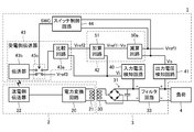
- FIG. 1 is a diagram showing a configuration of a wireless power transmission system 1 according to a first embodiment of the present invention.
- a wireless power transmission system 1 according to this embodiment includes a wireless power transmission device 2 and a wireless power reception device 3.
- the wireless power receiving device 3 is connected to a load 4 as shown in FIG.
- the load 4 is, for example, a secondary battery such as a lithium ion battery, and is mounted as a driving power source in a rechargeable device such as an electric vehicle or a smartphone.
- the wireless power transmission system 1 has a function of transmitting power wirelessly from the wireless power transmitting device 2 to the wireless power receiving device 3, and uses this function to charge the load 4.
- the wireless power transmission apparatus 2 includes a power conversion circuit 20, a power transmission coil 21, and a power transmission side transmitter 22.
- the wireless power receiving device 3 includes a power receiving coil 30, a rectifier circuit 31, a filter circuit 33, an input voltage detection circuit 40, an output voltage detection circuit 41, a target voltage generation circuit 42, and a power reception side transmitter 43. It is comprised.
- the power conversion circuit 20 has a function of converting DC power (not shown) supplied from the outside into AC power, and is configured to supply AC power obtained by the conversion to the power transmission coil 21. Specifically, the function of converting DC power into AC power is constituted by a switching power supply. The power conversion circuit 20 also has a function of controlling the output of the power transmission coil 21 by controlling AC power supplied to the power transmission coil 21 based on difference information described later. This will be described again later.
- the power transmission coil 21 is configured to receive AC power from the power conversion circuit 20 and generate an AC magnetic field. Power transmission by the wireless power transmission device 2 is realized by this alternating magnetic field. In addition, you may provide the capacitor
- the power transmission side transmitter 22 is a device having a communication function by, for example, Bluetooth (registered trademark), wireless LAN, optical coupling (photocoupler), magnetic coupling (coil), and the like, and receives differential information described later from the wireless power receiving device 3. And serves to supply the power conversion circuit 20.
- the power receiving coil 30 is configured to take in AC power via the AC magnetic field generated by the power transmitting coil 21. That is, when the AC magnetic field generated by the power transmission coil 21 is linked to the power receiving coil 30, AC power is generated in the power receiving coil 30 by electromagnetic induction.
- the power receiving coil 30 outputs the AC power thus generated to the rectifier circuit 31.
- a capacitor that forms a resonance circuit together with the power receiving coil 30 may be provided.
- the rectifier circuit 31 includes a bridge diode and a smoothing capacitor, and is a circuit that converts AC power received by the power receiving coil 30 into DC power and outputs the DC power to the load 4. Power transmission from the rectifier circuit 31 to the load 4 is realized using two transmission paths on the high-order side and the low-order side.
- the DC power output from the rectifier circuit 31 is not complete DC power but includes a certain amount of ripple voltage. This is because the power conversion circuit 20 is configured by a switching power supply.
- the filter circuit 33 is a low-pass filter provided to reduce the ripple voltage superimposed on the DC power output from the rectifier circuit 31, and is provided between the rectifier circuit 31 and the load 4. In the filter circuit 33, a delay and a voltage drop occur as described above.
- the wireless power receiving device 3 according to the present embodiment enables the feedback control of the voltage applied to the load 4 to be suitably performed while providing the filter circuit 33 having such properties in the previous stage of the load 4. is there.
- the input voltage detection circuit 40 is a circuit that detects the input voltage Vi of the filter circuit 33, and its input terminal is connected to the plus side input terminal of the filter circuit 33.
- the output voltage detection circuit 41 is a circuit that detects the output voltage Vo of the filter circuit 33, and its input terminal is connected to the plus side output terminal of the filter circuit 33.
- the input voltage detection circuit 40 is configured to detect the input voltage Vi as an effective value
- the output voltage detection circuit 41 is configured to detect the output voltage Vo as an effective value.
- the effective values of the input voltage Vi and the output voltage Vo alleviate the influence of the ripple voltage on the input voltage Vi and the output voltage Vo, thereby accurately setting the second target voltage Vref2 described later. This is so that it can be generated.
- the target voltage generation circuit 42 is a circuit that generates a second target voltage Vref2 that is a target value of the input voltage Vi based on the output voltage Vo and the first target voltage Vref1 that is the target value of the output voltage Vo. , A subtracting circuit 50a and an adding circuit 51.
- the first target voltage Vref1 is a fixed potential supplied from a power source (not shown) provided in the wireless power receiving apparatus 3.
- a specific value of the first target voltage Vref1 is set to an arbitrary positive value.
- the subtraction circuit 50a is a circuit that has two input terminals and calculates a difference between voltages supplied to them.
- the input voltage Vi and the output voltage Vo are respectively supplied to the two input terminals, and the subtraction circuit 50a is configured to calculate the difference between them. More specifically, the differential voltage Vi ⁇ Vo is calculated by subtracting the output voltage Vo from the input voltage Vi.
- the addition circuit 51 is a circuit that has two input terminals and adds the voltages supplied to them.
- each of the first target voltage Vref1 and the differential voltage Vi ⁇ Vo output from the subtraction circuit 50a is supplied to the two input terminals, and the adder circuit 51 adds them, Configured to output results.
- the output voltage of the adder circuit 51 is supplied to the power receiving side transmitter 43 as the second target voltage Vref2.
- the power-receiving-side transmitter 43 is a device having a communication function using, for example, Bluetooth (registered trademark), wireless LAN, optical coupling (photocoupler), magnetic coupling (coil), and the like, and the power-transmitting-side transmitter 22 in the wireless power transmission device 2. It is configured to be able to communicate with each other.
- the power-receiving-side transmitter 43 in the present embodiment receives the supply of the input voltage Vi from the input voltage detection circuit 40 and the supply of the second target voltage Vref2 from the target voltage generation circuit 42, and shows a difference indicating these differences. It plays a role of transmitting information to the wireless power transmission device 2.
- the difference information may be the input voltage Vi and the second target voltage Vref2 itself, or may be the difference voltage Vi ⁇ Vref2 between the input voltage Vi and the second target voltage Vref2.
- FIG. 2 is a diagram illustrating an internal configuration of the power-receiving-side transmitter 43 when the differential voltage Vi-Vref2 is transmitted as the differential information.
- the power receiving side transmitter 43 receives the input voltage Vi and the second target voltage Vref2, and generates a differential voltage Vi ⁇ Vref2, and a generated differential voltage Vi ⁇ .
- a transmission unit 43b configured to transmit Vref2 to the wireless power transmission device 2;
- FIG. 2B shows a detailed circuit configuration of the comparison circuit 43a.
- the comparison circuit 43a is configured by an error amplifier that detects, amplifies and outputs the difference between the input voltage Vi and the second target voltage Vref2. More specifically, the comparison circuit 43a includes an inverting input terminal to which the input voltage Vi is input, a non-inverting input terminal to which the second target voltage Vref2 is input, and an output from which the differential voltage Vi ⁇ Vref2 is output.
- An operational amplifier OP having a terminal, resistors R1, R2 and a capacitor C1 connected to the inverting input terminal of the operational amplifier, a resistor R3 and capacitors C2, C3 connected between the inverting input terminal and the output terminal of the operational amplifier.
- the resistor R1 and the capacitor C1 are connected in series, and the resistor R2 is connected in parallel with this series circuit.
- the resistor R3 and the capacitor C3 are connected in series, and the capacitor C2 is connected in parallel with this series circuit.
- the resistor R3 and the capacitors C2 and C3 constitute a negative feedback circuit of the operational amplifier OP.
- the time (target arrival time) required for the output of the comparison circuit 43a to reach the differential voltage Vi-Vref2 is determined by the values of the resistors R1 to R3 and the capacitors C1 to C3. fluctuate. That is, the ratio of the combined resistance value of the resistors R1 and R2 and the resistor R3 determines the magnification of the inverting amplifier circuit constituted by the operational amplifier OP, and the capacitor C3 is charged by the amount of negative feedback current depending on the value of the resistor R3. Since the time is determined, the target arrival time varies gently. As a result, sudden fluctuations in received power are suppressed. Therefore, stable power transmission is possible by appropriately setting the magnification and the charge time.
- the power conversion circuit 20 in the wireless power transmission device 2 controls the output of the power transmission coil 21 based on the difference information received from the wireless power reception device 3 in this way.
- the power transmission coil is set so that the input voltage Vi and the second target voltage Vref2 are equal (that is, the differential voltage Vi ⁇ Vref2 between the input voltage Vi and the second target voltage Vref2 is zero). 21 is controlled.
- Equation (1) above when the input voltage Vi is equal to the second target voltage Vref2, the output voltage Vo is equal to the first target voltage Vref1. Further, when the output voltage Vo decreases, the second target voltage Vref2 increases. Therefore, when the power conversion circuit 20 performs the above control, the input voltage Vi increases, and the output voltage Vo increases accordingly.
- the second voltage is increased in the direction of increasing the input voltage Vi.
- the second target voltage Vref2 can be generated in the direction of decreasing the input voltage Vi.
- the power converter circuit 20 in the wireless power transmission apparatus 2 performs output control of the power transmission coil 21 so that the 2nd target voltage Vref2 produced
- the target of feedback control is the input voltage Vi
- the above-described problem of lowering the feedback speed when the output voltage Vo is the target of feedback control does not occur.
- the output voltage Vo converges to the first target voltage Vref1
- the load is reduced by the drop voltage in the filter circuit 33 even though the feedback control target is the input voltage Vi.
- the problem that the voltage applied to 4 becomes small does not arise. Therefore, according to the wireless power receiving device 3 and the wireless power transmission system 1 according to the present embodiment, it can be said that feedback control when the filter circuit 33 is provided in the front stage of the load 4 can be suitably performed.
- the target voltage generation circuit 42 can suitably generate the second target voltage Vref2. It becomes possible.
- the input voltage Vi and the output voltage Vo are effective values, the influence of the ripple voltage on the input voltage Vi and the output voltage Vo can be reduced. Therefore, the second target voltage Vref2 can be generated with high accuracy.
- the power receiving side transmitter 43 may transmit an error signal to the wireless power transmitting apparatus 2 when the second target voltage Vref2 exceeds a predetermined reference value. According to this, it becomes possible to detect a failure of the filter circuit 33 on the wireless power transmitting apparatus 2 side.
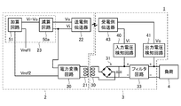
- FIG. 3 is a diagram showing a configuration of the wireless power transmission system 1 according to the second embodiment of the present invention.
- the input terminal of the input voltage detection circuit 40 is connected to the negative input terminal of the filter circuit 33
- the input terminal of the output voltage detection circuit 41 is the negative side of the filter circuit 33.
- the wireless power transmission system 1 according to the first embodiment is different from the wireless power transmission system 1 according to the first embodiment in that it is connected to the output terminal and the target voltage generation circuit 42 includes a subtraction circuit 50b instead of the subtraction circuit 50a.
- the same components as those of the first embodiment will be denoted by the same reference numerals, and description will be made focusing on differences from the first embodiment.
- the input terminal of the input voltage detection circuit 40 according to the present embodiment is connected to the negative input terminal of the filter circuit 33 as described above. Therefore, the voltage output from the input voltage detection circuit 40 in the present embodiment has a sign opposite to that in the first embodiment. That is, ⁇ Vi.
- the input terminal of the output voltage detection circuit 41 according to the present embodiment is connected to the negative output terminal of the filter circuit 33 as described above. Therefore, the voltage output from the output voltage detection circuit 41 in the present embodiment has a sign opposite to that in the first embodiment. That is, ⁇ Vo.
- the filter circuit 33 is a circuit that generates a voltage drop, Vi> Vo always holds. Therefore, the voltage
- the power receiving-side transmitter 43 in the present embodiment receives the supply of the voltage ⁇ Vi from the input voltage detection circuit 40 and the supply of the second target voltage Vref2 from the target voltage generation circuit 42, and based on these, the input voltage It plays a role of transmitting difference information indicating the difference between Vi (the voltage obtained by inverting the sign of the voltage ⁇ Vi supplied from the input voltage detection circuit 40) and the second target voltage Vref2 to the wireless power transmitting apparatus 2.
- the processing on the wireless power transmitting apparatus 2 side that has received this transmission is the same as that in the first embodiment.
- the wireless power transmission apparatus 2 performs the same processing as in the first embodiment, so that in the present embodiment as well, in the previous stage of the load 4 Feedback control when the filter circuit 33 is provided can be suitably performed.
- the input terminal of the input voltage detection circuit 40 is connected to the negative input terminal of the filter circuit 33, and the output voltage detection circuit
- the feedback control when the filter circuit 33 is provided in the front stage of the load 4 is preferably performed as in the first embodiment. It becomes possible to do.
- FIG. 4 is a diagram showing a configuration of a wireless power transmission system 1 according to the third embodiment of the present invention.
- the wireless power transmission system 1 according to the present embodiment differs from the wireless power transmission system 1 according to the first embodiment in terms of inputs of the subtraction circuit 50a and the addition circuit 51.
- the same components as those of the first embodiment will be denoted by the same reference numerals, and description will be made focusing on differences from the first embodiment.
- the first target voltage Vref1 and the output voltage Vo are supplied to the two input terminals of the subtraction circuit 50a according to the present embodiment. Based on these, the subtraction circuit 50a is configured to calculate a differential voltage Vref1-Vo obtained by subtracting the output voltage Vo from the first target voltage Vref1.
- the input voltage Vi and the differential voltage Vref1-Vo output from the subtraction circuit 50a are supplied to the two input terminals of the adder circuit 51 according to the present embodiment. Based on these, the adding circuit 51 is configured to add the differential voltage Vref1-Vo to the input voltage Vi. The result of the addition is supplied to the power receiving side transmitter 43 as the second target voltage Vref2.
- the second target voltage Vref2 supplied to the power-receiving-side transmitter 43 is expressed by the above formula (1). Therefore, when the wireless power transmission apparatus 2 performs the same processing as in the first embodiment, also in this embodiment, it is possible to suitably perform feedback control when the filter circuit 33 is provided in the previous stage of the load 4. become.
- the wireless power receiving apparatus 3 and the wireless power transmission system 1 according to the present embodiment are also suitable for the feedback control when the filter circuit 33 is provided in the front stage of the load 4 as in the first embodiment. It becomes possible to do.
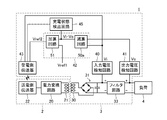
- FIG. 5 is a diagram showing a configuration of a wireless power transmission system 1 according to the fourth embodiment of the present invention.
- the wireless power transmission system 1 according to the present embodiment is different from the wireless power transmission system 1 according to the third embodiment in that it has a switch control circuit 44 and a switching circuit 43c in the power receiving side transmitter 43.
- a switch control circuit 44 and a switching circuit 43c in the power receiving side transmitter 43.
- Different the same components as those in the third embodiment will be denoted by the same reference numerals, and description will be made focusing on differences from the third embodiment.
- the power-receiving-side transmitter 43 includes a comparison circuit 43a, a transmission unit 43b, and a switching circuit 43c. Details of the comparison circuit 43a and the transmission unit 43b are the same as described with reference to FIG.
- the switching circuit 43c is a circuit that selects either the differential voltage Vi-Vref2 supplied from the comparison circuit 43a or the third target voltage Vref3 and supplies the selected voltage to the transmission unit 43b.
- the third target voltage Vref3 is a fixed potential supplied from a power source (not shown) provided in the wireless power receiving apparatus 3.
- a specific value of the third target voltage Vref3 is set to an arbitrary negative value.
- the transmission unit 43b transmits only one of the supplied voltages to the wireless power transmission device 2.
- the switch control circuit 44 is a circuit that generates a control signal SWC based on the first target voltage Vref1 and the output voltage Vo and supplies the control signal SWC to the switching circuit 43c.
- the switching circuit 43c is configured to select one of the differential voltage Vi ⁇ Vref2 and the third target voltage Vref3 according to the control signal SWC.
- the switching circuit 43c selects the third target voltage Vref3. In other cases (that is, when Vref1 ⁇ Vo), the switching circuit 43c generates the control signal SWC so as to select the differential voltage Vi ⁇ Vref2.
- the third target voltage Vref3 is transmitted to the wireless power transmitting apparatus 2 when Vref1> Vo, and the differential voltage Vi ⁇ Vref2 when Vref1 ⁇ Vo.
- the output control of the power transmission coil 21 is performed so that the third target voltage Vref3, which is a negative value, becomes zero. Will be executed. Since the third target voltage Vref3 is a fixed value, the output of the power transmission coil 21 gradually increases in this control, and as a result, the output voltage Vo also gradually increases. When the output voltage Vo thus increasing satisfies Vref1 ⁇ Vo, the differential voltage Vi ⁇ Vref2 is transmitted to the wireless power transmitting apparatus 2, and this time, control is performed in the direction of decreasing the output voltage Vo. As a result, the value of the output voltage Vo converges to the first target voltage Vref1.
- control different from that in the third embodiment is performed only when the output voltage Vo is smaller than the first target voltage Vref1. Since the control in that case is to fix the input of the wireless power transmitting apparatus 2 to the third target voltage Vref3, according to the present embodiment, the value of the third target voltage Vref3 is appropriately set. By doing so, it is possible to appropriately control the rate of increase of the output voltage Vo per unit time.
- the feedback control when the filter circuit 33 is provided in the previous stage of the load 4 can be suitably performed.
- FIG. 6 is a diagram showing a configuration of a wireless power transmission system 1 according to the fifth embodiment of the present invention.
- the wireless power transmission system 1 according to the present embodiment is different from the wireless power transmission system 1 according to the first embodiment in that a target voltage generation circuit 23 is provided instead of the target voltage generation circuit 42.
- a target voltage generation circuit 23 is provided instead of the target voltage generation circuit 42.
- the power receiving-side transmitter 43 is configured to transmit the input voltage Vi and the output voltage Vo to the wireless power transmitting apparatus 2 instead of the difference information indicating the difference between the input voltage Vi and the second target voltage Vref2. Is done.
- the power transmission side transmitter 22 receives the input voltage Vi and the output voltage Vo thus transmitted, and supplies them to the target voltage generation circuit 23.
- the target voltage generation circuit 23 is arranged in the wireless power transmitting apparatus 2 unlike the target voltage generation circuit 42 described in the first embodiment.
- the configuration and operation of the target voltage generation circuit 23 are the same as those of the target voltage generation circuit 42 described in the first embodiment, and the second target voltage Vref2 is generated using the subtraction circuit 50a and the addition circuit 51. It is configured as follows.
- the subtracting circuit 50 a is configured to calculate a differential voltage Vi ⁇ Vo between the input voltage Vi and the output voltage Vo supplied from the power transmission side transmitter 22.
- the adder circuit 51 is configured to add the first target voltage Vref1 and the differential voltage Vi ⁇ Vo output from the subtractor circuit 50a and output the sum as a second target voltage Vref2.
- the second target voltage Vref2 output from the adder circuit 51 is supplied to the power conversion circuit 20.
- the control performed by the power conversion circuit 20 that receives the supply of the second target voltage Vref2 is as described in the first embodiment, whereby the output voltage Vo can be converged to the first target voltage Vref1. Realized. Therefore, according to the present embodiment, it is possible to suitably perform feedback control when the filter circuit 33 is provided in the previous stage of the load 4.
- the wireless power receiving apparatus 3 and the wireless power transmission system 1 according to the present embodiment are also suitable for the feedback control when the filter circuit 33 is provided in the front stage of the load 4 as in the first embodiment. It becomes possible to do.
- the target voltage generation circuit 42 according to the first embodiment is replaced by the target voltage generation circuit 23 in the wireless power transmitting apparatus 2
- the first to fourth embodiments are described.
- the target voltage generation circuit 42 may be replaced with the target voltage generation circuit 23 in the wireless power transmitting apparatus 2 in the same manner.
- the switch control circuit 44, the comparison circuit 43a, and the switching circuit 43c are preferably replaced with similar circuits in the wireless power transmitting apparatus 2.
- FIG. 7 is a diagram showing a configuration of a wireless power transmission system 1 according to the sixth embodiment of the present invention.
- the wireless power transmission system 1 according to the present embodiment is different from the wireless power transmission system 1 according to the first embodiment in that it further includes a charging state detection circuit 45.
- the same components as those of the first embodiment will be denoted by the same reference numerals, and description will be made focusing on differences from the first embodiment.
- the charging state detection circuit 45 is a circuit that determines a charging state of the load 4 that is a secondary battery, based on a change in the differential voltage Vi ⁇ Vo output from the subtraction circuit 50a.
- the charge state detection circuit 45 makes this determination by utilizing the property of the differential voltage Vi ⁇ Vo that the value decreases as the charging of the load 4 proceeds.
- the charging state detection circuit 45 is configured to transmit information indicating the determination result to the wireless power transmission device 2 via the power receiving side transmitter 43.
- the wireless power transmission device 2 is configured to notify the user of the charging status of the load 4 based on the information thus transmitted.
- the wireless power receiving device 3 may notify the user of the charging status of the load 4 based on the determination result of the charging status detection circuit 45.
- the output of the feedback control circuit (specifically, the subtraction circuit 50a) is used to obtain the secondary battery. It becomes possible to grasp the charging status of a certain load 4. In addition, it becomes possible to notify the user of the grasped charging status.
- the target voltage generation circuit may be constituted by a microprocessor having functions of a subtraction circuit and an addition circuit.
- the first target voltage Vref1 is a fixed value stored in advance in a storage circuit (not shown).
Landscapes
- Engineering & Computer Science (AREA)
- Power Engineering (AREA)
- Computer Networks & Wireless Communication (AREA)
- Charge And Discharge Circuits For Batteries Or The Like (AREA)
- Transmitters (AREA)
Abstract
【課題】負荷4の前段にフィルタ回路33を設ける場合のフィードバック制御を好適に行う。 【解決手段】ワイヤレス受電装置3は、交流磁界を介して交流電力を取り込む受電コイル30と、受電コイル30が受電した交流電力を直流電力に変換して負荷に出力する整流回路31と、整流回路31と負荷4との間に設けられるフィルタ回路33と、フィルタ回路33の入力電圧Viを検出する入力電圧検知回路40と、フィルタ回路33の出力電圧Voを検出する出力電圧検知回路41と、出力電圧Vo及び該出力電圧Voの目標値である第1の目標電圧Vref1に基づいて、入力電圧Viの目標値である第2の目標電圧Vref2を生成する目標電圧生成回路42と、入力電圧Viと第2の目標電圧Vref2の差分を示す差分情報をワイヤレス送電装置2に伝達する受電側伝送器43と、を備える。
Description
本発明は、ワイヤレス受電装置及びワイヤレス電力伝送システムに関する。
ワイヤレス電力伝送技術による電力伝送を行えるように構成されたワイヤレス電力伝送システムが知られている。ワイヤレス電力伝送システムは、電力を送電する側のワイヤレス送電装置と、ワイヤレス送電装置によって送電された電力を受電するワイヤレス受電装置とを含んで構成される。
ワイヤレス電力伝送技術は、例えば、スマートフォンや電気自動車などに搭載される負荷(例えば、二次電池)の充電を行うために使用される。この場合、ワイヤレス送電装置は充電器であり、ワイヤレス受電装置はスマートフォンや電気自動車などに搭載される。ワイヤレス電力伝送技術により充電すべき負荷としては、リチウムイオンバッテリが主流である。
特許文献1には、ワイヤレス電力伝送システムの一例が開示されている。この例では、ワイヤレス受電装置内において、整流回路の後段にフィルタ回路が設けられる。このフィルタ回路は、ワイヤレス送電装置内のスイッチング電源の動作により発生するリップル電圧を軽減する役割を果たしている。
ところで、本願の発明者は、ワイヤレス電力伝送システムにおいて、負荷に印加する電圧のフィードバック制御を行うことを検討している。具体的には、負荷に印加する電圧がその目標電圧に等しくなるよう、ワイヤレス送電装置の出力を制御することを検討している。
しかしながら、検討を進めるうちに、特許文献1に記載されるようなフィルタ回路がワイヤレス受電装置内に存在すると、フィードバック制御が好適に行えなくなる場合があることが判明した。以下、詳しく説明する。
特許文献1に記載されるようなフィルタ回路をワイヤレス受電装置内に設ける場合、負荷にはフィルタ回路の出力電圧が印加されることになる。したがって、フィルタ回路の出力電圧をワイヤレス送電装置側に送れば一応はフィードバック制御が可能になるが、フィルタ回路では一般に遅延が発生するため、フィードバック速度が遅くなり、電力制御の安定性の確保が困難になる。そこで、フィルタ回路の入力電圧をワイヤレス送電装置側に送ることも考えられるが、そうすると今度は、負荷に印加される電圧が小さくなるという問題が発生する。すなわち、入力電圧は一般に、フィルタ回路での降下電圧分だけ出力電圧より大きくなる。したがって、入力電圧が目標電圧に等しくなるということは、フィルタ回路での降下電圧分だけ負荷に印加される電圧が小さくなる、ということを意味する。
したがって、本発明の目的の一つは、負荷の前段にフィルタ回路を設ける場合のフィードバック制御を好適に行えるワイヤレス受電装置及びワイヤレス電力伝送システムを提供することにある。
本発明によるワイヤレス受電装置は、ワイヤレス送電装置から伝送される電力をワイヤレスにて受電するワイヤレス受電装置であって、交流磁界を介して交流電力を取り込む受電コイルと、前記受電コイルが受電した交流電力を直流電力に変換して負荷に出力する整流回路と、前記整流回路と前記負荷との間に設けられるフィルタ回路と、前記フィルタ回路の入力電圧を検出する入力電圧検知回路と、前記フィルタ回路の出力電圧を検出する出力電圧検知回路と、前記出力電圧及び該出力電圧の目標値である第1の目標電圧に基づいて、前記入力電圧の目標値である第2の目標電圧を生成する目標電圧生成回路と、前記入力電圧と前記第2の目標電圧の差分を示す差分情報を前記ワイヤレス送電装置に伝達する受電側伝送器と、を備える、ワイヤレス受電装置である。
本発明によれば、出力電圧が第1の目標電圧より小さい場合には入力電圧を上げる方向に第2の目標電圧を生成し、出力電圧が第1の目標電圧より大きい場合には入力電圧を下げる方向に第2の目標電圧を生成することが可能になり、その結果として、入力電圧をフィードバック制御の対象としつつ、出力電圧を第1の目標電圧に収束させることが可能になる。したがって、負荷の前段にフィルタ回路を設ける場合のフィードバック制御を好適に行うことが可能になる。
上記ワイヤレス受電装置において、前記目標電圧生成回路は、前記入力電圧と前記出力電圧の差分電圧を算出する減算回路と、前記第1の目標電圧に前記差分電圧を加算することにより前記第2の目標電圧を生成する加算回路と、を有する、こととしてもよい。これによれば、目標電圧生成回路により、第2の目標電圧を好適に生成することが可能になる。
上記ワイヤレス受電装置において、前記目標電圧生成回路は、前記出力電圧と前記第1の目標電圧の差分電圧を算出する減算回路と、前記入力電圧に前記差分電圧を加算することにより前記第2の目標電圧を生成する加算回路と、を有する、こととしてもよい。これによっても、目標電圧生成回路により、第2の目標電圧を好適に生成することが可能になる。
上記各ワイヤレス受電装置においてさらに、前記受電側伝送器は、前記第2の目標電圧が基準値を超えたとき、前記ワイヤレス送電装置にエラー信号を伝達する、こととしてもよい。これによれば、フィルタ回路の故障を検知することが可能になる。
上記ワイヤレス受電装置においてさらに、前記差分電圧の変化に基づき、前記負荷の充電状況を判定する充電状態検出回路をさらに備える、こととしてもよい。これによれば、フィードバック制御用の回路の出力を利用して、二次電池である負荷の充電状況を把握することが可能になる。
上記各ワイヤレス受電装置においてさらに、前記入力電圧検知回路は前記入力電圧を実効値にて検出し、前記出力電圧検知回路は前記出力電圧を実効値にて検出する、こととしてもよい。これによれば、入力電圧及び出力電圧におけるリップル電圧の影響を軽減できるので、第2の目標電圧を精度よく生成することが可能になる。
本発明によるワイヤレス電力伝送システムは、ワイヤレス送電装置からワイヤレス受電装置にワイヤレスにて電力を伝送するワイヤレス電力伝送システムであって、前記ワイヤレス送電装置は、入力直流電力を交流電力に変換する電力変換回路と、前記電力変換回路から前記交流電力を受けて交流磁界を発生する送電コイルと、前記ワイヤレス受電装置と情報の伝達を行う送電側伝送器と、を備え、前記ワイヤレス受電装置は、上記各ワイヤレス受電装置のいずれかであり、前記電力変換回路は、前記受電側伝送器が送信し前記送電側伝送器が受信した前記差分情報に基づいて、前記送電コイルに供給する交流電力を制御する、ワイヤレス電力伝送システムである。
本発明によれば、出力電圧が第1の目標電圧より小さい場合には入力電圧を上げる方向に第2の目標電圧を生成し、出力電圧が第1の目標電圧より大きい場合には入力電圧を下げる方向に第2の目標電圧を生成することが可能になる。そして、こうして生成された第2の目標電圧と入力電圧とが等しくなるよう電力変換回路が送電コイルの出力制御を行うことにより、出力電圧を第1の目標電圧に収束させることが可能になる。したがって、負荷の前段にフィルタ回路を設ける場合のフィードバック制御を好適に行うことが可能になる。
本発明の他の一側面によるワイヤレス電力伝送システムは、ワイヤレス送電装置からワイヤレス受電装置にワイヤレスにて電力を伝送するワイヤレス電力伝送システムであって、前記ワイヤレス送電装置は、入力直流電力を交流電力に変換する電力変換回路と、前記電力変換回路から前記交流電力を受けて交流磁界を発生する送電コイルと、前記ワイヤレス受電装置と情報の伝達を行う送電側伝送器と、を備え、前記ワイヤレス受電装置は、交流磁界を介して交流電力を取り込む受電コイルと、前記受電コイルが受電した交流電力を直流電力に変換して負荷に出力する整流回路と、前記整流回路と前記負荷との間に設けられるフィルタ回路と、前記フィルタ回路の入力電圧を検出する入力電圧検知回路と、前記フィルタ回路の出力電圧を検出する出力電圧検知回路と、前記入力電圧及び前記出力電圧を前記ワイヤレス送電装置に伝達する受電側伝送器と、を備え、前記ワイヤレス送電装置は、前記出力電圧及び該出力電圧の目標値である第1の目標電圧に基づいて、前記入力電圧の目標値である第2の目標電圧を生成する目標電圧生成回路、をさらに備え、前記電力変換回路は、前記入力電圧と前記第2の目標電圧の差分を示す差分情報に基づいて、前記送電コイルに供給する交流電力を制御する、ワイヤレス電力伝送システムである。
本発明によっても、出力電圧が第1の目標電圧より小さい場合には入力電圧を上げる方向に第2の目標電圧を生成し、出力電圧が第1の目標電圧より大きい場合には入力電圧を下げる方向に第2の目標電圧を生成することが可能になる。そして、こうして生成された第2の目標電圧と入力電圧とが等しくなるよう電力変換回路が送電コイルの出力制御を行うことにより、出力電圧を第1の目標電圧に収束させることが可能になる。したがって、負荷の前段にフィルタ回路を設ける場合のフィードバック制御を好適に行うことが可能になる。
本発明によれば、負荷の前段にフィルタ回路を設ける場合のフィードバック制御を好適に行うことが可能になる。
以下、添付図面を参照しながら、本発明の実施の形態について詳細に説明する。
図1は、本発明の第1の実施の形態によるワイヤレス電力伝送システム1の構成を示す図である。同図に示すように、本実施の形態によるワイヤレス電力伝送システム1は、ワイヤレス送電装置2と、ワイヤレス受電装置3とを備えて構成される。
ワイヤレス受電装置3は、図1に示すように負荷4に接続される。負荷4は、例えばリチウムイオンバッテリなどの二次電池であり、電気自動車やスマートフォンなどの充電式装置に駆動用電源として搭載される。ワイヤレス電力伝送システム1は、ワイヤレス送電装置2からワイヤレス受電装置3に対してワイヤレスで送電を行う機能を有しており、この機能を利用して負荷4の充電を行う。
ワイヤレス送電装置2は、電力変換回路20と、送電コイル21と、送電側伝送器22とを有して構成される。また、ワイヤレス受電装置3は、受電コイル30と、整流回路31と、フィルタ回路33と、入力電圧検知回路40と、出力電圧検知回路41と、目標電圧生成回路42と、受電側伝送器43とを有して構成される。
電力変換回路20は、外部から供給される直流電力(図示せず)を交流電力に変換する機能を有し、変換によって得た交流電力を送電コイル21に供給するよう構成される。直流電力を交流電力に変換する機能は、具体的にはスイッチング電源によって構成される。電力変換回路20はまた、後述する差分情報に基づいて送電コイル21に供給する交流電力を制御することにより、送電コイル21の出力を制御する機能を有する。この点については、後ほど再度説明する。
送電コイル21は、電力変換回路20から交流電力を受けて交流磁界を発生するよう構成される。ワイヤレス送電装置2による電力の送電は、この交流磁界によって実現される。なお、送電コイル21と共に共振回路を構成するコンデンサを設けても構わない。
送電側伝送器22は、例えばブルートゥース(登録商標)、無線LAN、光結合(フォトカプラ)、磁気結合(コイル)などによる通信機能を有する装置であり、ワイヤレス受電装置3から後述する差分情報を受信し、電力変換回路20に供給する役割を果たす。
受電コイル30は、送電コイル21が生成した交流磁界を介して、交流電力を取り込むよう構成される。つまり、送電コイル21が生成した交流磁界が受電コイル30に鎖交すると、電磁誘導により受電コイル30に交流電力が発生する。受電コイル30は、こうして発生した交流電力を整流回路31に出力する。なお、受電コイル30と共に共振回路を構成するコンデンサを設けても構わない。
整流回路31は、ブリッジダイオードと平滑コンデンサを有し、受電コイル30が受電した交流電力を直流電力に変換して負荷4に出力する回路である。整流回路31から負荷4への電力伝送は、高位側と低位側の2本の伝送路を用いて実現される。整流回路31が出力する直流電力は完全な直流電力ではなく、ある程度のリップル電圧を含む。これは、電力変換回路20がスイッチング電源により構成されることによるものである。
フィルタ回路33は、整流回路31が出力する直流電力に重畳されるリップル電圧を軽減するために設けられるローパスフィルタであり、整流回路31と負荷4との間に設けられる。フィルタ回路33においては、上述したように遅延と電圧降下が発生する。本実施の形態によるワイヤレス受電装置3は、このような性質を有するフィルタ回路33を負荷4の前段に設けつつも、負荷4に印加する電圧のフィードバック制御を好適に行うことを可能にするものである。
入力電圧検知回路40は、フィルタ回路33の入力電圧Viを検出する回路であり、その入力端子はフィルタ回路33のプラス側入力端子に接続される。また、出力電圧検知回路41は、フィルタ回路33の出力電圧Voを検出する回路であり、その入力端子はフィルタ回路33のプラス側出力端子に接続される。入力電圧検知回路40は入力電圧Viを実効値にて検出し、出力電圧検知回路41は出力電圧Voを実効値にて検出するよう構成される。このように入力電圧Vi及び出力電圧Voのそれぞれを実効値とするのは、入力電圧Vi及び出力電圧Voにおけるリップル電圧の影響を軽減し、それによって、後述する第2の目標電圧Vref2を精度よく生成できるようにするためである。
目標電圧生成回路42は、出力電圧Vo及び該出力電圧Voの目標値である第1の目標電圧Vref1に基づいて、入力電圧Viの目標値である第2の目標電圧Vref2を生成する回路であり、減算回路50a及び加算回路51を有して構成される。なお、第1の目標電圧Vref1は、ワイヤレス受電装置3内に設けられる図示しない電源から供給される固定電位である。第1の目標電圧Vref1の具体的な値は、任意の正の値に設定される。
減算回路50aは、2つの入力端子を有し、これらに供給される電圧の差分を算出する回路である。本実施の形態においては、2つの入力端子には入力電圧Vi及び出力電圧Voのそれぞれが供給されており、減算回路50aは、これらの差分を算出するよう構成される。より具体的に言えば、入力電圧Viから出力電圧Voを減じてなる差分電圧Vi-Voを算出するよう構成される。
加算回路51は、2つの入力端子を有し、これらに供給される電圧を加算する回路である。本実施の形態においては、2つの入力端子には第1の目標電圧Vref1及び減算回路50aから出力される差分電圧Vi-Voのそれぞれが供給されており、加算回路51はこれらを加算し、その結果を出力するよう構成される。加算回路51の出力電圧は、第2の目標電圧Vref2として受電側伝送器43に供給される。
以上のようにして目標電圧生成回路42により生成される第2の目標電圧Vref2を数式を用いて表すと、次の式(1)となる。
Vref2=Vref1+Vi-Vo
=Vi-(Vo-Vref1) ・・・(1)
Vref2=Vref1+Vi-Vo
=Vi-(Vo-Vref1) ・・・(1)
受電側伝送器43は、例えばブルートゥース(登録商標)、無線LAN、光結合(フォトカプラ)、磁気結合(コイル)などによる通信機能を有する装置であり、ワイヤレス送電装置2内の送電側伝送器22と相互に通信可能に構成される。本実施の形態における受電側伝送器43は、入力電圧検知回路40から入力電圧Viの供給を受けるとともに、目標電圧生成回路42から第2の目標電圧Vref2の供給を受け、これらの差分を示す差分情報をワイヤレス送電装置2に伝達する役割を担う。差分情報は、具体的には、入力電圧Viと第2の目標電圧Vref2そのものであってもよいし、入力電圧Viと第2の目標電圧Vref2の差分電圧Vi-Vref2であってもよい。
図2は、差分情報として差分電圧Vi-Vref2を送信する場合における受電側伝送器43の内部構成を示す図である。同図(a)に示すように、受電側伝送器43は、入力電圧Vi及び第2の目標電圧Vref2を受けて差分電圧Vi-Vref2を生成する比較回路43aと、生成された差分電圧Vi-Vref2をワイヤレス送電装置2に向けて送信する伝送部43bとを有して構成される。
図2(b)には、比較回路43aの詳細な回路構成を示している。同図に示すように、比較回路43aは、入力電圧Viと第2の目標電圧Vref2の差を検出し、増幅して出力するエラーアンプによって構成される。より具体的に言えば、比較回路43aは、入力電圧Viが入力される反転入力端子、第2の目標電圧Vref2が入力される非反転入力端子、及び、差分電圧Vi-Vref2が出力される出力端子を有するオペアンプOPと、オペアンプの反転入力端子に接続される抵抗R1,R2及びキャパシタC1と、オペアンプの反転入力端子と出力端子の間に接続される抵抗R3及びキャパシタC2,C3とによって構成される。抵抗R1及びキャパシタC1は直列に接続され、抵抗R2は、この直列回路と並列に接続される。また、抵抗R3及びキャパシタC3は直列に接続され、キャパシタC2は、この直列回路と並列に接続される。抵抗R3及びキャパシタC2,C3は、オペアンプOPの負帰還回路を構成する。
このような比較回路43aの構成によれば、抵抗R1~R3及びキャパシタC1~C3それぞれの値によって、比較回路43aの出力が差分電圧Vi-Vref2に到達するまでに要する時間(目標到達時間)が変動する。つまり、抵抗R1,R2の合成抵抗値と抵抗R3との比率によりオペアンプOPによって構成される反転増幅回路の倍率が決まり、かつ、抵抗R3の値に依存する負帰還電流量によってキャパシタC3へのチャージ時間が決まることから、目標到達時間がなだらかに変動することになる。これにより、受電電力の急峻な変動が抑制される。したがって、倍率とチャージ時間の適切な設定によって、安定的な電力伝送が可能となる。
ワイヤレス送電装置2内の電力変換回路20は、こうしてワイヤレス受電装置3から受信される差分情報に基づいて、送電コイル21の出力を制御する。具体的には、入力電圧Viと第2の目標電圧Vref2とが等しくなるように(すなわち、入力電圧Viと第2の目標電圧Vref2の差分電圧Vi-Vref2がゼロとなるように)、送電コイル21の出力を制御する。上掲した式(1)によれば、入力電圧Viと第2の目標電圧Vref2とが等しいとき、出力電圧Voが第1の目標電圧Vref1に等しくなる。また、出力電圧Voが減少すると第2の目標電圧Vref2が増加するので、電力変換回路20が上記制御を行うと入力電圧Viが増加し、それに伴って出力電圧Voも増加する。逆に、出力電圧Voが増加すると第2の目標電圧Vref2が減少するので、電力変換回路20が上記制御を行うと入力電圧Viが減少し、それに伴って出力電圧Voも減少する。したがって、電力変換回路20が上記制御を行うことにより、出力電圧Voを第1の目標電圧Vref1に収束させることが実現される。
以上説明したように、本実施の形態によるワイヤレス受電装置3及びワイヤレス電力伝送システム1によれば、出力電圧Voが第1の目標電圧Vref1より小さい場合には入力電圧Viを上げる方向に第2の目標電圧Vref2を生成し、出力電圧Voが第1の目標電圧Vref1より大きい場合には入力電圧Viを下げる方向に第2の目標電圧Vref2を生成することが可能になる。そして、こうして生成された第2の目標電圧Vref2と入力電圧Viとが等しくなるようワイヤレス送電装置2内の電力変換回路20が送電コイル21の出力制御を行うので、出力電圧Voを第1の目標電圧Vref1に収束させることが可能になる。
フィードバック制御の対象が入力電圧Viであることから、本実施の形態では、上述したフィードバック速度の低下という、出力電圧Voをフィードバック制御の対象とする場合の問題は発生しない。また、出力電圧Voが第1の目標電圧Vref1に収束するのであるから、本実施の形態では、フィードバック制御の対象が入力電圧Viであるにも関わらず、フィルタ回路33での降下電圧分だけ負荷4に印加される電圧が小さくなるという問題も生じない。したがって、本実施の形態によるワイヤレス受電装置3及びワイヤレス電力伝送システム1によれば、負荷4の前段にフィルタ回路33を設ける場合のフィードバック制御を好適に行うことが可能になると言える。
また、本実施の形態によれば、目標電圧生成回路42内に減算回路50a及び加算回路51を設けているので、目標電圧生成回路42により、第2の目標電圧Vref2を好適に生成することが可能になる。
また、本実施の形態によれば、入力電圧Vi及び出力電圧Voのそれぞれを実効値としているので、入力電圧Vi及び出力電圧Voにおけるリップル電圧の影響を軽減できる。したがって、第2の目標電圧Vref2を精度よく生成することが可能になる。
なお、受電側伝送器43は、第2の目標電圧Vref2が予め定められた基準値を超えたとき、ワイヤレス送電装置2にエラー信号を伝達することとしてもよい。これによれば、ワイヤレス送電装置2側において、フィルタ回路33の故障を検知することが可能になる。
図3は、本発明の第2の実施の形態によるワイヤレス電力伝送システム1の構成を示す図である。本実施の形態によるワイヤレス電力伝送システム1は、入力電圧検知回路40の入力端子がフィルタ回路33のマイナス側入力端子に接続される点、出力電圧検知回路41の入力端子がフィルタ回路33のマイナス側出力端子に接続される点、及び、目標電圧生成回路42が減算回路50aに代えて減算回路50bを有する点で、第1の実施の形態によるワイヤレス電力伝送システム1と異なる。以下、第1の実施の形態と同一の構成には同一の符号を付し、第1の実施の形態との相違点を中心に説明する。
本実施の形態による入力電圧検知回路40の入力端子は、上記したようにフィルタ回路33のマイナス側入力端子に接続される。したがって、本実施の形態において入力電圧検知回路40から出力される電圧は、第1の実施の形態とは逆の符号を有することになる。つまり、-Viとなる。
同様に、本実施の形態による出力電圧検知回路41の入力端子は、上記したようにフィルタ回路33のマイナス側出力端子に接続される。したがって、本実施の形態において出力電圧検知回路41から出力される電圧は、第1の実施の形態とは逆の符号を有することになる。つまり、-Voとなる。
本実施の形態による減算回路50bは、入力電圧検知回路40の出力電圧(=-Vi)から出力電圧検知回路41の出力電圧(=-Vo)を減じてなる差分電圧-Vi-(-Vo)の絶対値|-Vi-(-Vo)|を算出する回路である。ここで、フィルタ回路33は電圧降下を発生させる回路であるので、Vi>Voが常に成り立つ。したがって、減算回路50bが出力する電圧|-Vi-(-Vo)|は、第1の実施の形態において減算回路50aが出力する差分電圧Vi-Voと常に同じ値になるので、上掲した式(1)は本実施の形態でも成立する。
本実施の形態における受電側伝送器43は、入力電圧検知回路40から電圧-Viの供給を受けるとともに、目標電圧生成回路42から第2の目標電圧Vref2の供給を受け、これらに基づき、入力電圧Vi(入力電圧検知回路40から供給を受けた電圧-Viの符号を反転させてなる電圧)と第2の目標電圧Vref2の差分を示す差分情報をワイヤレス送電装置2に伝達する役割を担う。この伝達を受けたワイヤレス送電装置2側の処理は、第1の実施の形態と同様である。上掲した式(1)が本実施の形態でも成立することから、ワイヤレス送電装置2が第1の実施の形態と同様の処理を行うことにより、本実施の形態においても、負荷4の前段にフィルタ回路33を設ける場合のフィードバック制御を好適に行うことが可能になる。
以上説明したように、本実施の形態によるワイヤレス受電装置3及びワイヤレス電力伝送システム1によれば、入力電圧検知回路40の入力端子をフィルタ回路33のマイナス側入力端子に接続し、出力電圧検知回路41の入力端子をフィルタ回路33のマイナス側出力端子に接続しているにも関わらず、第1の実施の形態と同様に、負荷4の前段にフィルタ回路33を設ける場合のフィードバック制御を好適に行うことが可能になる。
図4は、本発明の第3の実施の形態によるワイヤレス電力伝送システム1の構成を示す図である。本実施の形態によるワイヤレス電力伝送システム1は、減算回路50a及び加算回路51それぞれの入力の点で、第1の実施の形態によるワイヤレス電力伝送システム1と異なる。以下、第1の実施の形態と同一の構成には同一の符号を付し、第1の実施の形態との相違点を中心に説明する。
本実施の形態による減算回路50aの2つの入力端子には、第1の目標電圧Vref1及び出力電圧Voのそれぞれが供給される。減算回路50aは、これらに基づき、第1の目標電圧Vref1から出力電圧Voを減じてなる差分電圧Vref1-Voを算出するよう構成される。
本実施の形態による加算回路51の2つの入力端子には、入力電圧Vi及び減算回路50aから出力される差分電圧Vref1-Voのそれぞれが供給される。加算回路51は、これらに基づき、入力電圧Viに差分電圧Vref1-Voを加算するよう構成される。加算の結果は、第2の目標電圧Vref2として受電側伝送器43に供給される。
こうして受電側伝送器43に供給される第2の目標電圧Vref2は、上掲した式(1)で表される。したがって、ワイヤレス送電装置2が第1の実施の形態と同様の処理を行うことにより、本実施の形態においても、負荷4の前段にフィルタ回路33を設ける場合のフィードバック制御を好適に行うことが可能になる。
以上説明したように、本実施の形態によるワイヤレス受電装置3及びワイヤレス電力伝送システム1によっても、第1の実施の形態と同様に、負荷4の前段にフィルタ回路33を設ける場合のフィードバック制御を好適に行うことが可能になる。
図5は、本発明の第4の実施の形態によるワイヤレス電力伝送システム1の構成を示す図である。本実施の形態によるワイヤレス電力伝送システム1は、スイッチ制御回路44を有する点、及び、受電側伝送器43内に切替回路43cを有する点で、第3の実施の形態によるワイヤレス電力伝送システム1と異なる。以下、第3の実施の形態と同一の構成には同一の符号を付し、第3の実施の形態との相違点を中心に説明する。
本実施の形態による受電側伝送器43は、比較回路43aと、伝送部43bと、切替回路43cとを有して構成される。このうち比較回路43a及び伝送部43bの詳細は、図2を参照して説明したとおりである。
切替回路43cは、比較回路43aから供給される差分電圧Vi-Vref2と、第3の目標電圧Vref3とのいずれか一方を選択し、伝送部43bに供給する回路である。なお、第3の目標電圧Vref3は、ワイヤレス受電装置3内に設けられる図示しない電源から供給される固定電位である。第3の目標電圧Vref3の具体的な値は、任意の負の値に設定される。伝送部43bは、こうして供給された一方の電圧のみをワイヤレス送電装置2に伝送する。
スイッチ制御回路44は、第1の目標電圧Vref1及び出力電圧Voに基づいて制御信号SWCを生成し、切替回路43cに供給する回路である。切替回路43cは、この制御信号SWCに従って、差分電圧Vi-Vref2と第3の目標電圧Vref3とのいずれか一方を選択するよう構成される。
具体的に説明すると、スイッチ制御回路44は、第1の目標電圧Vref1が出力電圧Voより大きい場合(すなわち、Vref1>Voである場合)に、切替回路43cが第3の目標電圧Vref3を選択するよう制御信号SWCを生成し、それ以外の場合(すなわち、Vref1≦Voである場合)に、切替回路43cが差分電圧Vi-Vref2を選択するよう制御信号SWCを生成する。これにより、ワイヤレス送電装置2に伝送されるのは、Vref1>Voである場合には第3の目標電圧Vref3となり、Vref1≦Voである場合には差分電圧Vi-Vref2となる。
ワイヤレス送電装置2に差分電圧Vi-Vref2が伝送される場合のワイヤレス電力伝送システム1の動作は、第3の実施の形態と同様である。すなわち、差分電圧Vi-Vref2がゼロとなるように送電コイル21の出力制御が実行され、その結果として、出力電圧Voの値が第1の目標電圧Vref1に収束する。この制御は、差分電圧Vi-Vref2の値(=Vo-Vref1)が常に非負であることから、出力電圧Voを下げる方向での制御となる。
一方、ワイヤレス送電装置2に第3の目標電圧Vref3が伝送される場合のワイヤレス電力伝送システム1は、負の値である第3の目標電圧Vref3がゼロとなるように、送電コイル21の出力制御を実行することになる。第3の目標電圧Vref3は固定値であるので、この制御では送電コイル21の出力が徐々に増加し、その結果として、出力電圧Voも徐々に増加する。こうして増加する出力電圧VoがVref1≦Voを満たしたとき、ワイヤレス送電装置2に差分電圧Vi-Vref2が伝送されるようになり、今度は出力電圧Vo下げる方向に制御が行われることになる。結果として、出力電圧Voの値は第1の目標電圧Vref1に収束する。
つまり、本実施の形態では、出力電圧Voが第1の目標電圧Vref1より小さい場合にのみ、第3の実施の形態と異なる制御を行うようにしている。そして、その場合の制御は、ワイヤレス送電装置2の入力を第3の目標電圧Vref3に固定するというものであるので、本実施の形態によれば、第3の目標電圧Vref3の値を適切に設定することにより、出力電圧Voの単位時間あたりの上昇率を適切に制御することが可能になる。
以上説明したように、本実施の形態によるワイヤレス受電装置3及びワイヤレス電力伝送システム1によれば、負荷4の前段にフィルタ回路33を設ける場合のフィードバック制御を好適に行うことが可能になるという第3の実施の形態と同様の効果に加え、出力電圧Voの単位時間あたりの上昇率を適切に制御できる、というさらなる効果を得ることが可能になる。
図6は、本発明の第5の実施の形態によるワイヤレス電力伝送システム1の構成を示す図である。本実施の形態によるワイヤレス電力伝送システム1は、目標電圧生成回路42に代えて目標電圧生成回路23を有する点で、第1の実施の形態によるワイヤレス電力伝送システム1と異なる。以下、第1の実施の形態と同一の構成には同一の符号を付し、第1の実施の形態との相違点を中心に説明する。
本実施の形態による受電側伝送器43は、入力電圧Viと第2の目標電圧Vref2の差分を示す差分情報ではなく、入力電圧Vi及び出力電圧Voをワイヤレス送電装置2に対して送信するよう構成される。送電側伝送器22は、こうして送信された入力電圧Vi及び出力電圧Voを受信し、目標電圧生成回路23に供給する。
目標電圧生成回路23は、第1の実施の形態で説明した目標電圧生成回路42とは異なり、ワイヤレス送電装置2内に配置される。目標電圧生成回路23の構成及び動作は第1の実施の形態で説明した目標電圧生成回路42のものと同一であり、減算回路50a及び加算回路51を用いて第2の目標電圧Vref2を生成するよう構成される。
すなわち、減算回路50aは、送電側伝送器22から供給される入力電圧Vi及び出力電圧Voの差分電圧Vi-Voを算出するよう構成される。また、加算回路51は、第1の目標電圧Vref1及び減算回路50aから出力される差分電圧Vi-Voを加算し、第2の目標電圧Vref2として出力するよう構成される。加算回路51から出力された第2の目標電圧Vref2は、電力変換回路20に供給される。第2の目標電圧Vref2の供給を受けた電力変換回路20が行う制御は第1の実施の形態で説明したとおりであり、これにより、出力電圧Voを第1の目標電圧Vref1に収束させることが実現される。したがって、本実施の形態によっても、負荷4の前段にフィルタ回路33を設ける場合のフィードバック制御を好適に行うことが可能になる。
以上説明したように、本実施の形態によるワイヤレス受電装置3及びワイヤレス電力伝送システム1によっても、第1の実施の形態と同様に、負荷4の前段にフィルタ回路33を設ける場合のフィードバック制御を好適に行うことが可能になる。
なお、本実施の形態では、第1の実施の形態による目標電圧生成回路42をワイヤレス送電装置2内の目標電圧生成回路23により置き換えた例を説明したが、第1~第4の実施の形態による目標電圧生成回路42を同様にワイヤレス送電装置2内の目標電圧生成回路23に置き換えてもよいことは勿論である。なお、この場合において、図5に示した第4の実施の形態に関しては、スイッチ制御回路44、比較回路43a、及び切替回路43cもワイヤレス送電装置2内の同様の回路に置き換えることが好ましい。
図7は、本発明の第6の実施の形態によるワイヤレス電力伝送システム1の構成を示す図である。本実施の形態によるワイヤレス電力伝送システム1は、充電状態検出回路45をさらに有する点で、第1の実施の形態によるワイヤレス電力伝送システム1と異なる。以下、第1の実施の形態と同一の構成には同一の符号を付し、第1の実施の形態との相違点を中心に説明する。
充電状態検出回路45は、減算回路50aが出力する差分電圧Vi-Voの変化に基づき、二次電池である負荷4の充電状況を判定する回路である。充電状態検出回路45は、負荷4の充電が進行するにつれて値が小さくなるという差分電圧Vi-Voの性質を利用して、この判定を行う。
充電状態検出回路45は、判定結果を示す情報を、受電側伝送器43を介してワイヤレス送電装置2に伝達するよう構成される。ワイヤレス送電装置2は、こうして伝達された情報に基づき、ユーザに対して負荷4の充電状況を通知するよう構成される。なお、ワイヤレス受電装置3においても同様に、充電状態検出回路45の判定結果に基づき、ユーザに対して負荷4の充電状況を通知することとしてもよい。
以上説明したように、本実施の形態によるワイヤレス受電装置3及びワイヤレス電力伝送システム1によれば、フィードバック制御用の回路(具体的には減算回路50a)の出力を利用して、二次電池である負荷4の充電状況を把握することが可能になる。また、把握した充電状況をユーザに通知することが可能になる。
以上、本発明の好ましい実施の形態について説明したが、本発明はこうした実施の形態に何等限定されるものではなく、本発明が、その要旨を逸脱しない範囲において、種々なる態様で実施され得ることは勿論である。
例えば、目標電圧生成回路は、減算回路と加算回路の機能を有するマイクロプロセッサ等から構成されていても構わない。この場合、第1の目標電圧Vref1は、図示しない記憶回路に予め記憶される固定値となる。
1 ワイヤレス電力伝送システム
2 ワイヤレス送電装置
3 ワイヤレス受電装置
4 負荷
20 電力変換回路
21 送電コイル
22 送電側伝送器
23,42 目標電圧生成回路
30 受電コイル
31 整流回路
33 フィルタ回路
40 入力電圧検知回路
41 出力電圧検知回路
43 受電側伝送器
43a 比較回路
43b 伝送部
43c 切替回路
44 スイッチ制御回路
45 充電状態検出回路
50a,50b 減算回路
51 加算回路
SWC 制御信号
Vi フィルタ回路33の入力電圧
Vo フィルタ回路33の出力電圧
Vref1 第1の目標電圧
Vref2 第2の目標電圧
Vref3 第3の目標電圧
2 ワイヤレス送電装置
3 ワイヤレス受電装置
4 負荷
20 電力変換回路
21 送電コイル
22 送電側伝送器
23,42 目標電圧生成回路
30 受電コイル
31 整流回路
33 フィルタ回路
40 入力電圧検知回路
41 出力電圧検知回路
43 受電側伝送器
43a 比較回路
43b 伝送部
43c 切替回路
44 スイッチ制御回路
45 充電状態検出回路
50a,50b 減算回路
51 加算回路
SWC 制御信号
Vi フィルタ回路33の入力電圧
Vo フィルタ回路33の出力電圧
Vref1 第1の目標電圧
Vref2 第2の目標電圧
Vref3 第3の目標電圧
Claims (8)
- ワイヤレス送電装置から伝送される電力をワイヤレスにて受電するワイヤレス受電装置であって、
交流磁界を介して交流電力を取り込む受電コイルと、
前記受電コイルが受電した交流電力を直流電力に変換して負荷に出力する整流回路と、
前記整流回路と前記負荷との間に設けられるフィルタ回路と、
前記フィルタ回路の入力電圧を検出する入力電圧検知回路と、
前記フィルタ回路の出力電圧を検出する出力電圧検知回路と、
前記出力電圧及び該出力電圧の目標値である第1の目標電圧に基づいて、前記入力電圧の目標値である第2の目標電圧を生成する目標電圧生成回路と、
前記入力電圧と前記第2の目標電圧の差分を示す差分情報を前記ワイヤレス送電装置に伝達する受電側伝送器と、
を備える、ワイヤレス受電装置。 - 前記目標電圧生成回路は、
前記入力電圧と前記出力電圧の差分電圧を算出する減算回路と、
前記第1の目標電圧に前記差分電圧を加算することにより前記第2の目標電圧を生成する加算回路と、を有する、
請求項1に記載のワイヤレス受電装置。 - 前記目標電圧生成回路は、
前記出力電圧と前記第1の目標電圧の差分電圧を算出する減算回路と、
前記入力電圧に前記差分電圧を加算することにより前記第2の目標電圧を生成する加算回路と、を有する、
請求項1に記載のワイヤレス受電装置。 - 前記受電側伝送器は、前記第2の目標電圧が基準値を超えたとき、前記ワイヤレス送電装置にエラー信号を伝達する、
請求項2又は3に記載のワイヤレス受電装置。 - 前記差分電圧の変化に基づき、前記負荷の充電状況を判定する充電状態検出回路をさらに備える、
請求項2に記載のワイヤレス受電装置。 - 前記入力電圧検知回路は前記入力電圧を実効値にて検出し、
前記出力電圧検知回路は前記出力電圧を実効値にて検出する、
請求項1乃至5のいずれか一項に記載のワイヤレス受電装置。 - ワイヤレス送電装置からワイヤレス受電装置にワイヤレスにて電力を伝送するワイヤレス電力伝送システムであって、
前記ワイヤレス送電装置は、
入力直流電力を交流電力に変換する電力変換回路と、
前記電力変換回路から前記交流電力を受けて交流磁界を発生する送電コイルと、
前記ワイヤレス受電装置と情報の伝達を行う送電側伝送器と、を備え、
前記ワイヤレス受電装置は、請求項1乃至6のいずれか一項に記載のワイヤレス受電装置であり、
前記電力変換回路は、前記受電側伝送器が送信し前記送電側伝送器が受信した前記差分情報に基づいて、前記送電コイルに供給する交流電力を制御する、
ワイヤレス電力伝送システム。 - ワイヤレス送電装置からワイヤレス受電装置にワイヤレスにて電力を伝送するワイヤレス電力伝送システムであって、
前記ワイヤレス送電装置は、
入力直流電力を交流電力に変換する電力変換回路と、
前記電力変換回路から前記交流電力を受けて交流磁界を発生する送電コイルと、
前記ワイヤレス受電装置と情報の伝達を行う送電側伝送器と、を備え、
前記ワイヤレス受電装置は、
交流磁界を介して交流電力を取り込む受電コイルと、
前記受電コイルが受電した交流電力を直流電力に変換して負荷に出力する整流回路と、
前記整流回路と前記負荷との間に設けられるフィルタ回路と、
前記フィルタ回路の入力電圧を検出する入力電圧検知回路と、
前記フィルタ回路の出力電圧を検出する出力電圧検知回路と、
前記入力電圧及び前記出力電圧を前記ワイヤレス送電装置に伝達する受電側伝送器と、を備え、
前記ワイヤレス送電装置は、前記出力電圧及び該出力電圧の目標値である第1の目標電圧に基づいて、前記入力電圧の目標値である第2の目標電圧を生成する目標電圧生成回路、をさらに備え、
前記電力変換回路は、前記入力電圧と前記第2の目標電圧の差分を示す差分情報に基づいて、前記送電コイルに供給する交流電力を制御する、
ワイヤレス電力伝送システム。
Priority Applications (4)
| Application Number | Priority Date | Filing Date | Title |
|---|---|---|---|
| US16/488,827 US10910887B2 (en) | 2017-03-31 | 2017-03-31 | Wireless power receiving device and wireless power transmission system |
| CN201780089120.5A CN110462975B (zh) | 2017-03-31 | 2017-03-31 | 无线受电装置和无线电力传输系统 |
| JP2019508109A JP6741144B2 (ja) | 2017-03-31 | 2017-03-31 | ワイヤレス受電装置及びワイヤレス電力伝送システム |
| PCT/JP2017/013602 WO2018179337A1 (ja) | 2017-03-31 | 2017-03-31 | ワイヤレス受電装置及びワイヤレス電力伝送システム |
Applications Claiming Priority (1)
| Application Number | Priority Date | Filing Date | Title |
|---|---|---|---|
| PCT/JP2017/013602 WO2018179337A1 (ja) | 2017-03-31 | 2017-03-31 | ワイヤレス受電装置及びワイヤレス電力伝送システム |
Publications (1)
| Publication Number | Publication Date |
|---|---|
| WO2018179337A1 true WO2018179337A1 (ja) | 2018-10-04 |
Family
ID=63677761
Family Applications (1)
| Application Number | Title | Priority Date | Filing Date |
|---|---|---|---|
| PCT/JP2017/013602 Ceased WO2018179337A1 (ja) | 2017-03-31 | 2017-03-31 | ワイヤレス受電装置及びワイヤレス電力伝送システム |
Country Status (4)
| Country | Link |
|---|---|
| US (1) | US10910887B2 (ja) |
| JP (1) | JP6741144B2 (ja) |
| CN (1) | CN110462975B (ja) |
| WO (1) | WO2018179337A1 (ja) |
Cited By (1)
| Publication number | Priority date | Publication date | Assignee | Title |
|---|---|---|---|---|
| JP2021510052A (ja) * | 2018-11-30 | 2021-04-08 | 北京小米移動軟件有限公司Beijing Xiaomi Mobile Software Co.,Ltd. | 無線充電装置の制御方法、制御装置及び無線充電装置 |
Citations (3)
| Publication number | Priority date | Publication date | Assignee | Title |
|---|---|---|---|---|
| WO2015182274A1 (ja) * | 2014-05-30 | 2015-12-03 | 株式会社Ihi | 送電装置及び非接触給電システム |
| JP2015231308A (ja) * | 2014-06-06 | 2015-12-21 | 株式会社Ihi | 受電装置及び非接触給電システム |
| JP2016119759A (ja) * | 2014-12-19 | 2016-06-30 | 株式会社Ihi | 非接触給電システム及び送電装置 |
Family Cites Families (15)
| Publication number | Priority date | Publication date | Assignee | Title |
|---|---|---|---|---|
| FI20095973A0 (fi) * | 2009-09-22 | 2009-09-22 | Powerkiss Oy | Induktiivinen tehonsyöttö |
| CN102195366B (zh) * | 2010-03-19 | 2014-03-12 | Tdk株式会社 | 无线馈电装置以及无线电力传输系统 |
| KR101222749B1 (ko) * | 2010-12-14 | 2013-01-16 | 삼성전기주식회사 | 무선 전력 전송 장치 및 그 전송 방법 |
| JP5884698B2 (ja) | 2012-09-28 | 2016-03-15 | トヨタ自動車株式会社 | 非接触受電装置 |
| KR101979459B1 (ko) * | 2012-12-03 | 2019-05-16 | 엘에스전선 주식회사 | 무선 전력 전송 시스템, 무선 전력 수신 장치 및 무선 전력 수신 방법 |
| CN105340154B (zh) * | 2013-07-12 | 2018-06-19 | 株式会社 Ihi | 电力传输系统 |
| EP3032698B1 (en) * | 2013-07-31 | 2018-10-24 | Panasonic Corporation | Wireless power-transfer system and power-transmission device |
| JP6141171B2 (ja) * | 2013-11-08 | 2017-06-07 | 京セラ株式会社 | 送電装置及び無線電力伝送システム |
| US9692238B2 (en) * | 2014-02-18 | 2017-06-27 | Panasonic Corporation | Wireless power transmission system and power transmitting device |
| KR102187437B1 (ko) * | 2014-03-11 | 2020-12-08 | 엘지이노텍 주식회사 | 무선전력 전송 장치를 구비한 무선전력전송 시스템 |
| JP2015203684A (ja) * | 2014-04-16 | 2015-11-16 | 株式会社豊田自動織機 | 非接触電力伝送装置、送電機器及び受電機器 |
| JP6328479B2 (ja) * | 2014-04-28 | 2018-05-23 | マクセルホールディングス株式会社 | ワイヤレス電力伝送装置 |
| JP6707526B2 (ja) * | 2015-04-14 | 2020-06-10 | 東海旅客鉄道株式会社 | コンバータ及び受電装置 |
| CN104993621A (zh) * | 2015-07-27 | 2015-10-21 | 南京理工大学紫金学院 | 一种基于zvs谐振磁耦合式无线输电装置 |
| WO2017042904A1 (ja) * | 2015-09-09 | 2017-03-16 | 株式会社 東芝 | 無線電力伝送システム、送電装置および受電装置 |
-
2017
- 2017-03-31 JP JP2019508109A patent/JP6741144B2/ja not_active Expired - Fee Related
- 2017-03-31 US US16/488,827 patent/US10910887B2/en active Active
- 2017-03-31 WO PCT/JP2017/013602 patent/WO2018179337A1/ja not_active Ceased
- 2017-03-31 CN CN201780089120.5A patent/CN110462975B/zh active Active
Patent Citations (3)
| Publication number | Priority date | Publication date | Assignee | Title |
|---|---|---|---|---|
| WO2015182274A1 (ja) * | 2014-05-30 | 2015-12-03 | 株式会社Ihi | 送電装置及び非接触給電システム |
| JP2015231308A (ja) * | 2014-06-06 | 2015-12-21 | 株式会社Ihi | 受電装置及び非接触給電システム |
| JP2016119759A (ja) * | 2014-12-19 | 2016-06-30 | 株式会社Ihi | 非接触給電システム及び送電装置 |
Cited By (3)
| Publication number | Priority date | Publication date | Assignee | Title |
|---|---|---|---|---|
| JP2021510052A (ja) * | 2018-11-30 | 2021-04-08 | 北京小米移動軟件有限公司Beijing Xiaomi Mobile Software Co.,Ltd. | 無線充電装置の制御方法、制御装置及び無線充電装置 |
| JP7002553B2 (ja) | 2018-11-30 | 2022-01-20 | 北京小米移動軟件有限公司 | 無線充電装置の制御方法、制御装置及び無線充電装置 |
| US11342779B2 (en) | 2018-11-30 | 2022-05-24 | Beijing Xiaomi Mobile Software Co., Ltd. | Wireless charging apparatus and control method and control device therefor |
Also Published As
| Publication number | Publication date |
|---|---|
| JP6741144B2 (ja) | 2020-08-19 |
| CN110462975A (zh) | 2019-11-15 |
| US20200067354A1 (en) | 2020-02-27 |
| US10910887B2 (en) | 2021-02-02 |
| JPWO2018179337A1 (ja) | 2020-02-06 |
| CN110462975B (zh) | 2023-02-28 |
Similar Documents
| Publication | Publication Date | Title |
|---|---|---|
| JP6391144B2 (ja) | ワイヤレス充電システム、デバイス、および方法 | |
| US9866051B2 (en) | Adaptive charger to maximize charge rate | |
| JP6206579B2 (ja) | 給電装置及び非接触給電システム | |
| US11139700B2 (en) | Leakage detector, wireless power transmitting device, wireless power receiving device, and wireless power transmission system | |
| US9627986B2 (en) | Power conversion device and power conversion method | |
| US9438126B2 (en) | Power conversion device and power conversion method | |
| JP2013192326A (ja) | 非接触給電装置 | |
| WO2014061241A1 (ja) | 受電制御回路、ワイヤレス受電装置の制御方法、電子機器 | |
| US20150295502A1 (en) | Power conversion device and power conversion method | |
| JP2018102054A (ja) | 非接触受電装置及び非接触電力伝送システム | |
| CN103091532A (zh) | 用于汽车的基于零磁通补偿的电流传感器 | |
| CN107959358B (zh) | 一种无线充电装置的控制方法及无线充电装置 | |
| US10985616B2 (en) | Contactless transmitter | |
| JP2015220817A (ja) | 直流電力供給装置 | |
| JP6741144B2 (ja) | ワイヤレス受電装置及びワイヤレス電力伝送システム | |
| JP2017060328A (ja) | 非接触受電装置及び電力伝送システム | |
| JP2017032349A (ja) | 二次電池状態検出装置 | |
| EP3989397B1 (en) | Foreign objection detection sensing circuit for wireless power transmission systems | |
| JP6565809B2 (ja) | 送電装置及び電力伝送システム | |
| JP2016220293A (ja) | 非接触送電装置 | |
| WO2014069148A1 (ja) | 非接触電力伝送装置および受電機器 | |
| JP2016208630A (ja) | 充電装置 | |
| US12573884B2 (en) | Wireless power transmission system comprising wireless power receiver and wireless power device | |
| JP2017093089A (ja) | 送電装置、受電装置及び電力伝送システム | |
| TWM331243U (en) | Power supply equipment, and its cooperative receiver |
Legal Events
| Date | Code | Title | Description |
|---|---|---|---|
| 121 | Ep: the epo has been informed by wipo that ep was designated in this application |
Ref document number: 17904188 Country of ref document: EP Kind code of ref document: A1 |
|
| ENP | Entry into the national phase |
Ref document number: 2019508109 Country of ref document: JP Kind code of ref document: A |
|
| NENP | Non-entry into the national phase |
Ref country code: DE |
|
| 122 | Ep: pct application non-entry in european phase |
Ref document number: 17904188 Country of ref document: EP Kind code of ref document: A1 |