WO2018173144A1 - 電力変換装置 - Google Patents
電力変換装置 Download PDFInfo
- Publication number
- WO2018173144A1 WO2018173144A1 PCT/JP2017/011405 JP2017011405W WO2018173144A1 WO 2018173144 A1 WO2018173144 A1 WO 2018173144A1 JP 2017011405 W JP2017011405 W JP 2017011405W WO 2018173144 A1 WO2018173144 A1 WO 2018173144A1
- Authority
- WO
- WIPO (PCT)
- Prior art keywords
- voltage
- level
- control
- signal
- inverter
- Prior art date
Links
Images


Classifications
-
- H—ELECTRICITY
- H02—GENERATION; CONVERSION OR DISTRIBUTION OF ELECTRIC POWER
- H02M—APPARATUS FOR CONVERSION BETWEEN AC AND AC, BETWEEN AC AND DC, OR BETWEEN DC AND DC, AND FOR USE WITH MAINS OR SIMILAR POWER SUPPLY SYSTEMS; CONVERSION OF DC OR AC INPUT POWER INTO SURGE OUTPUT POWER; CONTROL OR REGULATION THEREOF
- H02M1/00—Details of apparatus for conversion
- H02M1/32—Means for protecting converters other than automatic disconnection
-
- H—ELECTRICITY
- H02—GENERATION; CONVERSION OR DISTRIBUTION OF ELECTRIC POWER
- H02J—CIRCUIT ARRANGEMENTS OR SYSTEMS FOR SUPPLYING OR DISTRIBUTING ELECTRIC POWER; SYSTEMS FOR STORING ELECTRIC ENERGY
- H02J3/00—Circuit arrangements for ac mains or ac distribution networks
- H02J3/18—Arrangements for adjusting, eliminating or compensating reactive power in networks
- H02J3/1821—Arrangements for adjusting, eliminating or compensating reactive power in networks using shunt compensators
- H02J3/1835—Arrangements for adjusting, eliminating or compensating reactive power in networks using shunt compensators with stepless control
- H02J3/1842—Arrangements for adjusting, eliminating or compensating reactive power in networks using shunt compensators with stepless control wherein at least one reactive element is actively controlled by a bridge converter, e.g. active filters
- H02J3/1857—Arrangements for adjusting, eliminating or compensating reactive power in networks using shunt compensators with stepless control wherein at least one reactive element is actively controlled by a bridge converter, e.g. active filters wherein such bridge converter is a multilevel converter
-
- H—ELECTRICITY
- H02—GENERATION; CONVERSION OR DISTRIBUTION OF ELECTRIC POWER
- H02M—APPARATUS FOR CONVERSION BETWEEN AC AND AC, BETWEEN AC AND DC, OR BETWEEN DC AND DC, AND FOR USE WITH MAINS OR SIMILAR POWER SUPPLY SYSTEMS; CONVERSION OF DC OR AC INPUT POWER INTO SURGE OUTPUT POWER; CONTROL OR REGULATION THEREOF
- H02M1/00—Details of apparatus for conversion
- H02M1/42—Circuits or arrangements for compensating for or adjusting power factor in converters or inverters
-
- H—ELECTRICITY
- H02—GENERATION; CONVERSION OR DISTRIBUTION OF ELECTRIC POWER
- H02M—APPARATUS FOR CONVERSION BETWEEN AC AND AC, BETWEEN AC AND DC, OR BETWEEN DC AND DC, AND FOR USE WITH MAINS OR SIMILAR POWER SUPPLY SYSTEMS; CONVERSION OF DC OR AC INPUT POWER INTO SURGE OUTPUT POWER; CONTROL OR REGULATION THEREOF
- H02M7/00—Conversion of ac power input into dc power output; Conversion of dc power input into ac power output
- H02M7/42—Conversion of dc power input into ac power output without possibility of reversal
- H02M7/44—Conversion of dc power input into ac power output without possibility of reversal by static converters
- H02M7/48—Conversion of dc power input into ac power output without possibility of reversal by static converters using discharge tubes with control electrode or semiconductor devices with control electrode
- H02M7/483—Converters with outputs that each can have more than two voltages levels
- H02M7/4835—Converters with outputs that each can have more than two voltages levels comprising two or more cells, each including a switchable capacitor, the capacitors having a nominal charge voltage which corresponds to a given fraction of the input voltage, and the capacitors being selectively connected in series to determine the instantaneous output voltage
-
- H—ELECTRICITY
- H02—GENERATION; CONVERSION OR DISTRIBUTION OF ELECTRIC POWER
- H02M—APPARATUS FOR CONVERSION BETWEEN AC AND AC, BETWEEN AC AND DC, OR BETWEEN DC AND DC, AND FOR USE WITH MAINS OR SIMILAR POWER SUPPLY SYSTEMS; CONVERSION OF DC OR AC INPUT POWER INTO SURGE OUTPUT POWER; CONTROL OR REGULATION THEREOF
- H02M7/00—Conversion of ac power input into dc power output; Conversion of dc power input into ac power output
- H02M7/42—Conversion of dc power input into ac power output without possibility of reversal
- H02M7/44—Conversion of dc power input into ac power output without possibility of reversal by static converters
- H02M7/48—Conversion of dc power input into ac power output without possibility of reversal by static converters using discharge tubes with control electrode or semiconductor devices with control electrode
- H02M7/483—Converters with outputs that each can have more than two voltages levels
- H02M7/4837—Flying capacitor converters
-
- H—ELECTRICITY
- H02—GENERATION; CONVERSION OR DISTRIBUTION OF ELECTRIC POWER
- H02M—APPARATUS FOR CONVERSION BETWEEN AC AND AC, BETWEEN AC AND DC, OR BETWEEN DC AND DC, AND FOR USE WITH MAINS OR SIMILAR POWER SUPPLY SYSTEMS; CONVERSION OF DC OR AC INPUT POWER INTO SURGE OUTPUT POWER; CONTROL OR REGULATION THEREOF
- H02M7/00—Conversion of ac power input into dc power output; Conversion of dc power input into ac power output
- H02M7/42—Conversion of dc power input into ac power output without possibility of reversal
- H02M7/44—Conversion of dc power input into ac power output without possibility of reversal by static converters
- H02M7/48—Conversion of dc power input into ac power output without possibility of reversal by static converters using discharge tubes with control electrode or semiconductor devices with control electrode
- H02M7/53—Conversion of dc power input into ac power output without possibility of reversal by static converters using discharge tubes with control electrode or semiconductor devices with control electrode using devices of a triode or transistor type requiring continuous application of a control signal
- H02M7/537—Conversion of dc power input into ac power output without possibility of reversal by static converters using discharge tubes with control electrode or semiconductor devices with control electrode using devices of a triode or transistor type requiring continuous application of a control signal using semiconductor devices only, e.g. single switched pulse inverters
- H02M7/5387—Conversion of dc power input into ac power output without possibility of reversal by static converters using discharge tubes with control electrode or semiconductor devices with control electrode using devices of a triode or transistor type requiring continuous application of a control signal using semiconductor devices only, e.g. single switched pulse inverters in a bridge configuration
- H02M7/53871—Conversion of dc power input into ac power output without possibility of reversal by static converters using discharge tubes with control electrode or semiconductor devices with control electrode using devices of a triode or transistor type requiring continuous application of a control signal using semiconductor devices only, e.g. single switched pulse inverters in a bridge configuration with automatic control of output voltage or current
-
- H—ELECTRICITY
- H02—GENERATION; CONVERSION OR DISTRIBUTION OF ELECTRIC POWER
- H02M—APPARATUS FOR CONVERSION BETWEEN AC AND AC, BETWEEN AC AND DC, OR BETWEEN DC AND DC, AND FOR USE WITH MAINS OR SIMILAR POWER SUPPLY SYSTEMS; CONVERSION OF DC OR AC INPUT POWER INTO SURGE OUTPUT POWER; CONTROL OR REGULATION THEREOF
- H02M1/00—Details of apparatus for conversion
- H02M1/0003—Details of control, feedback or regulation circuits
- H02M1/0025—Arrangements for modifying reference values, feedback values or error values in the control loop of a converter
-
- H—ELECTRICITY
- H02—GENERATION; CONVERSION OR DISTRIBUTION OF ELECTRIC POWER
- H02M—APPARATUS FOR CONVERSION BETWEEN AC AND AC, BETWEEN AC AND DC, OR BETWEEN DC AND DC, AND FOR USE WITH MAINS OR SIMILAR POWER SUPPLY SYSTEMS; CONVERSION OF DC OR AC INPUT POWER INTO SURGE OUTPUT POWER; CONTROL OR REGULATION THEREOF
- H02M1/00—Details of apparatus for conversion
- H02M1/0067—Converter structures employing plural converter units, other than for parallel operation of the units on a single load
- H02M1/007—Plural converter units in cascade
-
- H—ELECTRICITY
- H02—GENERATION; CONVERSION OR DISTRIBUTION OF ELECTRIC POWER
- H02M—APPARATUS FOR CONVERSION BETWEEN AC AND AC, BETWEEN AC AND DC, OR BETWEEN DC AND DC, AND FOR USE WITH MAINS OR SIMILAR POWER SUPPLY SYSTEMS; CONVERSION OF DC OR AC INPUT POWER INTO SURGE OUTPUT POWER; CONTROL OR REGULATION THEREOF
- H02M1/00—Details of apparatus for conversion
- H02M1/32—Means for protecting converters other than automatic disconnection
- H02M1/322—Means for rapidly discharging a capacitor of the converter for protecting electrical components or for preventing electrical shock
-
- H—ELECTRICITY
- H02—GENERATION; CONVERSION OR DISTRIBUTION OF ELECTRIC POWER
- H02M—APPARATUS FOR CONVERSION BETWEEN AC AND AC, BETWEEN AC AND DC, OR BETWEEN DC AND DC, AND FOR USE WITH MAINS OR SIMILAR POWER SUPPLY SYSTEMS; CONVERSION OF DC OR AC INPUT POWER INTO SURGE OUTPUT POWER; CONTROL OR REGULATION THEREOF
- H02M1/00—Details of apparatus for conversion
- H02M1/32—Means for protecting converters other than automatic disconnection
- H02M1/325—Means for protecting converters other than automatic disconnection with means for allowing continuous operation despite a fault, i.e. fault tolerant converters
-
- Y—GENERAL TAGGING OF NEW TECHNOLOGICAL DEVELOPMENTS; GENERAL TAGGING OF CROSS-SECTIONAL TECHNOLOGIES SPANNING OVER SEVERAL SECTIONS OF THE IPC; TECHNICAL SUBJECTS COVERED BY FORMER USPC CROSS-REFERENCE ART COLLECTIONS [XRACs] AND DIGESTS
- Y02—TECHNOLOGIES OR APPLICATIONS FOR MITIGATION OR ADAPTATION AGAINST CLIMATE CHANGE
- Y02E—REDUCTION OF GREENHOUSE GAS [GHG] EMISSIONS, RELATED TO ENERGY GENERATION, TRANSMISSION OR DISTRIBUTION
- Y02E40/00—Technologies for an efficient electrical power generation, transmission or distribution
- Y02E40/20—Active power filtering [APF]
Definitions
- the present invention relates to a power conversion device, and more particularly to a power conversion device coupled to a power system.
- Patent Document 1 discloses a power converter called MMCC (Modular Multilevel Cascade Converter).
- MMCC Modular Multilevel Cascade Converter
- This power conversion device is used as, for example, a reactive power compensation device, and includes three arms that are delta-connected.
- Each arm includes a plurality of capacitors and a plurality of cascaded inverters.
- Each inverter includes a plurality of semiconductor switching elements, and exchanges power between a corresponding capacitor and a power system.
- the inverter operation is stopped when the DC voltage of the capacitor exceeds the protection level below the allowable level, and the inverter operation is restarted when the DC voltage of the capacitor drops to a return level below the protection level due to natural discharge.
- a method is conceivable. However, this method has a problem that the time for reducing the DC voltage of the capacitor to the return level becomes long and the stop time of the inverter becomes long.
- a series connection of a resistor element and a switch is connected in parallel to the capacitor, the switch is turned on when the DC voltage of the capacitor exceeds the protection level, and a current flows from the capacitor to the resistor element.
- a method for rapidly reducing the DC voltage is conceivable (see FIG. 12).
- a main object of the present invention is to provide a small-sized power conversion device capable of quickly restarting the operation of the inverter even when an accident occurs in the power system.
- the power conversion device includes a capacitor, an inverter that transfers power between the capacitor and the power system, and a first DC voltage control for the inverter so that the DC voltage of the capacitor becomes a first command value. And a second control unit that performs reactive power control of the inverter so that the reactive power exchanged between the capacitor and the power system becomes the second command value.
- the first and second control units stop the DC voltage control and the reactive power control, respectively, in response to the DC voltage exceeding a protection level higher than the first command value.
- the first control unit resumes the DC voltage control in response to the DC voltage having dropped below the first return level below the protection level.
- the second control unit resumes the reactive power control in response to the direct current voltage dropping below the second return level that is lower than the first return level.
- the inverter operation is stopped when the DC voltage of the capacitor exceeds the protection level, and only the DC voltage control of the inverter is resumed when the DC voltage drops below the first return level.
- the DC voltage is quickly reduced, and the inverter reactive power control is resumed when the DC voltage drops below the second return level. Therefore, even when an accident occurs in the power system, the operation of the inverter can be resumed quickly.
- the apparatus can be reduced in size as compared with the case where the series connection body of the resistor element and the switch is connected in parallel to the capacitor.
- FIG. 2 is a circuit block diagram illustrating a configuration of a signal generation circuit included in the control device illustrated in FIG. 1. It is a block diagram which shows the structure of the reactive power deviation calculating part contained in the control apparatus shown in FIG. It is a block diagram which shows the structure of the direct-current voltage control part and the reactive power control part which are contained in the control apparatus shown in FIG. It is a block diagram which shows the structure of the electric current control part contained in the control apparatus shown in FIG. It is a block diagram which shows the structure of the inverse DQ converter contained in the control apparatus shown in FIG.
- FIG. 9 It is a circuit diagram which shows the structure of the gate signal generation circuit contained in the control apparatus shown in FIG. 9 is a time chart illustrating waveforms of the AC voltage command value Vuvr, the carrier signal Cuv, and the gate signals Auv and Buv illustrated in FIG. 8. 10 is a time chart illustrating the operation of the power conversion device shown in FIGS. 1 to 9; It is a time chart for demonstrating the comparative example of this Embodiment. It is a circuit diagram which shows the other comparative example of this Embodiment.
- FIG. 1 is a circuit block diagram showing a configuration of a power converter according to an embodiment of the present invention.
- this power converter is used as a reactive power compensator for compensating reactive power of the power system 1, and switches S1 to S6, transformers 2 and 3, current limiting resistors R1 to R3, AC line UL, VL, WL, current transformers C1 to C3, reactors L1 to L3, arms A1 to A3, and a control device 4 are provided.
- switches S1 to S3 are connected to the three-phase transmission lines 1u, 1v, 1w of the power system 1, respectively, and the other terminals are connected to the three primary windings of the transformer 2, respectively.
- Switches S1 to S3 are normally turned on, and are turned off, for example, during maintenance of the power converter.
- the transformer 2 includes three primary windings and three secondary windings, and transmits and receives three-phase AC power.
- One terminals of the current limiting resistors R1 to R3 are respectively connected to three secondary windings of the transformer 2, and the other terminals thereof are respectively connected to one terminals of the AC lines UL, VL, WL.
- Current limiting resistors R1 to R3 limit the current flowing from power system 1 to arms A1 to A3 when the power converter is activated.
- the switches S4 to S6 are connected in parallel to the current limiting resistors R1 to R3, respectively, and are turned on after the current flowing through the arms A1 to A3 is stabilized when the power converter is activated.
- the transformer 3 feeds back the AC voltages Vu, Vv, Vw having values corresponding to the AC voltages of the AC lines UL, VL, WL to the control device 4.
- Reactor L1 and arm A1 are connected in series between the other terminal of AC line UL and the other terminal of AC line VL.
- Reactor L2 and arm A2 are connected in series between the other terminal of AC line VL and the other terminal of AC line WL.
- Reactor L3 and arm A3 are connected in series between the other terminal of AC line WL and the other terminal of AC line UL. That is, the arms A1 to A3 are delta connected.
- Reactors L1 to L3 suppress the circulating current flowing through arms A1 to A3.
- Reactors L1 to L3 may be provided separately from arms A1 to A3, or may be inductance components of arms A1 to A3.
- the arms A1 to A3 are controlled by the control device 4 and generate three-phase AC power.
- Current transformers C1 to C3 feed back AC currents Iuv, Ivw, and Iwu having values corresponding to the AC currents flowing through arms A1 to A3 to control device 4, respectively.
- Each of the arms A1 to A3 includes a plurality (for example, 20) of unit converters 5 connected in cascade.
- Each of the plurality of unit converters 5 generates AC power in accordance with a control signal from the control device 4 or the like.
- FIG. 2 is a circuit block diagram showing the configuration of the unit converter 5.
- the unit converter 5 includes AC terminals 5 a and 5 b, a switch S ⁇ b> 7, an inverter 10, DC lines PL and NL, a capacitor 15, a voltage detector 16 (first detector), and a control unit 17.
- the AC terminals 5a of the first stage unit converters 5 of the arms A1 to A3 are connected to the other terminals of the AC lines UL, VL, and WL through the reactors L1 to L3, respectively.
- the AC terminal 5b of the final stage unit converter 5 of the arms A1 to A3 is connected to the other terminal of the AC lines VL, WL, and UL, respectively.
- the AC terminal 5a of each other unit converter 5 is connected to the AC terminal 5b of the previous unit converter 5, and the AC terminal 5b is connected to the AC terminal 5a of the next unit converter 5.
- the switch S7 is connected between the AC terminals 5a and 5b and is controlled by the control device 4, for example.
- the switch S7 is turned off when the corresponding unit converter 5 is normal, and is turned on when the corresponding unit converter 5 fails.
- the switch S7 is turned on, the AC terminals 5a and 5b are short-circuited, and the corresponding unit converter 5 is bypassed.
- the inverter 10 includes IGBTs (Insulated Gate Bipolar Transistors) 11 to 14 and diodes D1 to D4.
- the collectors of IGBTs 11 and 12 are both connected to positive DC line PL, and their emitters are connected to AC terminals 5a and 5b, respectively.
- the collectors of the IGBTs 13 and 14 are connected to the AC terminals 5a and 5b, respectively, and their emitters are both connected to the negative DC line NL.
- Each gate of IGBTs 11 to 14 receives a gate signal from control unit 17.
- Diodes D1-D4 are connected in antiparallel to IGBTs 11-14, respectively.
- the inverter 10 is subjected to DC voltage control and reactive power control by the control device 4 and the control unit 17, and transfers power between the power system 1 and the capacitor 15.
- Capacitor 15 is connected between DC lines PL and NL and stores DC power.
- the voltage detector 16 outputs a DC voltage VDC having a value corresponding to the DC voltage between the terminals of the capacitor 15 to the control unit 17.
- the control unit 17 is connected to the DC lines PL and NL, and is driven by the DC power stored in the capacitor 15.
- the control unit 17 operates the inverter 10 based on the gate signals Auv, Buv, Avw, Bvw, Awu, and Bwu from the control device 4, and sends a signal indicating the DC voltage VDC from the voltage detector 16 to the control device 4. Send.
- the control device 4 includes a reactive power command value Qr, AC voltages Vu, Vv, Vw from the transformer 3, AC currents Iuv, Ivw, Iwu from the current transformers C1 to C3, and unit converters. 5, each of the three arms A1 to A3 (that is, each of the 60 unit converters 5) is controlled.
- Reactive power command value Qr is given from the central command room of power system 1, for example.
- the power converter supplies reactive power having a value corresponding to the reactive power command value Qr to the power system 1.
- FIG. 3 is a circuit block diagram showing the configuration of the signal generation circuit 20 included in the control device 4.
- the signal generation circuit 20 includes a monitor voltage generation unit 21 and comparators 22-24.
- the monitor voltage generation unit 21 generates the monitor voltage VM based on the DC voltage VDC from the 60 unit converters 5. For example, the monitor voltage generator 21 selects the highest DC voltage VDC among the 60 DC voltages VDC, and outputs the selected DC voltage VDC as the monitor voltage VM.
- the comparator 22 compares the monitor voltage VM with the level of the protection level VH, and generates a protection signal P based on the comparison result.
- the protection signal P is set to the “H” level of the inactivation level.
- monitor voltage VM is higher than protection level VH (VM> VH)
- protection signal P is set to the “L” level of the activation level.
- the protection level VH is lower than the allowable level and higher than the rated value and command value of the DC voltage VDC.
- the comparator 23 compares the monitor voltage VM with the level of the return level V1 ( ⁇ VH), and generates the return signal B1 based on the comparison result.
- the return signal B1 is set to the inactivation level “H” level.
- the return signal B1 is set to the “L” level of the activation level.
- the return level V1 is a voltage lower than the protection level VH and higher than the rated value and the command value of the DC voltage VDC. After the electric power system 1 returns to normal from the accident, it is necessary to quickly restart the operation of the power converter. However, if the reactive power control of the inverter 10 is resumed immediately when the DC voltage VDC of the capacitor 15 becomes lower than the protection level VH, the reactive power is supplied from the power converter to the power system 1 and the voltage of the power system 1 increases. Then, the DC voltage VDC of the capacitor 15 rises again and exceeds the protection level VH. As a result, the operation and stop of the inverter 10 are repeated, and the power conversion device does not operate normally.
- the comparator 24 compares the monitor voltage VM with the level of the return level V2 ( ⁇ V1), and generates the return signal B2 based on the comparison result.
- monitor voltage VM is higher than return level V2 (VM> V2)
- return signal B2 is set to the inactivation level “H” level.
- the monitor voltage VM is equal to or lower than the return level V2 (VM ⁇ V2)
- the return signal B2 is set to the “L” level of the activation level.
- the return level V2 is a voltage lower than the return level V1 and higher than the rated value and the command value of the DC voltage VDC. Even if the voltage of the electric power system 1 rises and the DC voltage VDC of the capacitor 15 rises again because the reactive power control of the inverter 10 is resumed, the return level V2 does not cause the DC voltage VDC to exceed the protection level VH. It is set to such a value.
- FIG. 4 is a block diagram illustrating a configuration of the reactive power deviation calculation unit 30 included in the control device 4.
- the reactive power deviation calculation unit 30 includes a calculator 31, DQ converters 32 and 33, a reactive power calculator 34, and a subtractor 35.
- the computing unit 31 obtains AC currents Iu, Iv, Iw at a level corresponding to the AC current flowing in the AC lines UL, VL, WL based on the AC currents Iuv, Ivw, Iwu from the current transformers C1 to C3.
- the DQ converter 32 converts the three-phase alternating currents Iu, Iv, and Iw into a d-axis current Id and a q-axis current Iq.
- the DQ converter 33 converts the three-phase AC voltages Vu, Vv, Vw from the transformer 3 into a d-axis voltage Vd and a q-axis voltage Vq.
- the reactive power calculator 34 determines the reactive power Q based on the d-axis current Id, the q-axis current Iq, the d-axis voltage Vd, and the q-axis voltage Vq.
- the control device 4 further generates a DC voltage command value VDCr corresponding to the 60 unit converters 5.
- the DC voltage command value VDCr is given to 60 unit converters 5.
- DC voltage command value VDCr is normally set to a rated DC voltage.
- FIGS. 5A and 5B are block diagrams showing configurations of the DC voltage control unit 40 and the reactive power control unit 45.
- the DC voltage control unit 40 includes a flip-flop 41, a subtractor 42, a switching circuit 43, and a PI (Proportional Integral) control unit 44.
- DC voltage control unit 40 constitutes a first control unit that performs DC voltage control of inverter 10 such that DC voltage VDC of capacitor 15 becomes DC voltage command value VDCr.
- the flip-flop 41 is reset when both the protection signal P and the return signal B1 are at “H” level, and sets the output signal ⁇ 41 to “L” level (0).
- the flip-flop 41 is set when the protection signal P falls from the “H” level to the “L” level, and raises the output signal ⁇ 41 from the “L” level (0) to the “H” level (1).
- Signal ⁇ 41 is applied to each of switching circuit 43 and PI control unit 44.
- the switching circuit 43 gives the deviation ⁇ VDC from the subtractor 42 to the PI control unit 44 when the signal ⁇ 41 is at the “L” level (0), and “0” when the signal ⁇ 41 is at the “H” level (1). Is given to the PI control unit 44.
- the PI control unit 44 adds a value proportional to the output value ( ⁇ VDC or 0) of the switching circuit 43 and a value obtained by integrating the output value to generate a d-axis current command value Idr.
- signal ⁇ 41 is at “L” level (0)
- PI control unit 44 adds a value proportional to deviation ⁇ VDC from switching circuit 43 and a value obtained by integrating deviation ⁇ VDC to obtain d-axis current command value Idr. And the DC voltage of the inverter 10 is controlled.
- the reactive power control unit 45 includes a flip-flop 46, a switching circuit 47, and a PI control unit 48, as shown in FIG.
- the reactive power control unit 45 and the reactive power deviation calculation unit 30 of FIG. 4 perform reactive power control of the inverter 10 so that the reactive power Q exchanged between the capacitor 15 and the power system 1 becomes the reactive power command value Qr.
- the 2nd control part to perform is comprised.
- the flip-flop 46 is reset when the protection signal P and the return signal B2 are both at the “H” level, and sets the output signal ⁇ 46 to the “L” level (0).
- the flip-flop 46 is set when the protection signal P falls from the “H” level to the “L” level, and raises the output signal ⁇ 46 from the “L” level (0) to the “H” level (1).
- Signal ⁇ 46 is applied to each of switching circuit 47 and PI control unit 48.
- Switching circuit 47 provides reactive power deviation ⁇ Q from control device 4 to PI controller 48 when signal ⁇ 46 is at “L” level (0), and when signal ⁇ 46 is at “H” level (1). “0” is given to the PI control unit 48.
- the PI controller 48 adds a value proportional to the output value ( ⁇ Q or 0) of the switching circuit 47 and a value obtained by integrating the output value to generate a q-axis current command value Iqr.
- the PI control unit 48 adds the value proportional to the deviation ⁇ Q from the switching circuit 47 and the value obtained by integrating the deviation ⁇ Q to obtain the q-axis current command value Iqr. And the reactive power control of the inverter 10 is performed.
- FIGS. 6A and 6B are block diagrams showing the configuration of the current control units 50 and 60.
- the current control unit 50 includes a subtractor 51, a PI control unit 52, and an adder 53, as shown in FIG.
- the PI control unit 52 is controlled by the output signal ⁇ 41 of the flip-flop 41 (FIG. 5A).
- the PI control unit 52 adds the value proportional to the deviation ⁇ Id and the value obtained by integrating the deviation ⁇ Id to generate the d-axis voltage Vd1.
- the integral value in PI control unit 52 is reset to 0, and d-axis voltage Vd1 is fixed to 0.
- the adder 53 adds the d-axis voltage Vd from the DQ converter 33 to the d-axis voltage Vd1 from the PI control unit 52 to generate a d-axis voltage command value Vdr.
- the current control unit 60 includes a subtractor 61, a PI control unit 62, and an adder 63, as shown in FIG.
- the PI control unit 62 is controlled by the output signal ⁇ 41 of the flip-flop 41.
- the PI control unit 62 adds the value proportional to the deviation ⁇ Iq and the value obtained by integrating the deviation ⁇ Iq to generate the q-axis voltage Vq1.
- the signal ⁇ 41 is at “H” level (1), the integral value in the PI control unit 62 is reset to 0, and the q-axis voltage Vq1 is fixed to 0.
- Adder 63 adds q-axis voltage Vq from DQ converter 33 to q-axis voltage Vq1 from PI control unit 62 to generate q-axis voltage command value Vqr.
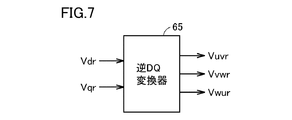
- FIG. 7 is a block diagram showing the configuration of the inverse DQ converter 65.
- the inverse DQ converter 65 performs inverse DQ conversion on the d-axis voltage command value Vdr and the q-axis voltage command value Vqr from the current control units 50 and 60 to obtain three-phase AC voltage command values Vuvr, Vvwr, and Vwur. Convert.
- Each of the three-phase AC voltage command values Vuvr, Vvwr, and Vwur is a sine wave, and the phases of the three-phase AC voltage command values Vuvr, Vvwr, and Vwur are shifted by 120 degrees.
- FIG. 8A, 8B, and 8C are circuit diagrams showing the configuration of the gate signal generation circuits 70, 80, and 90.
- the gate signal generation circuit 70 includes a comparator 72, a buffer 73, inverters 74 and 75, and AND gates 76 and 77.
- the comparator 72 compares the level of the AC voltage command value Vuvr and the level of the carrier signal Cuv, and outputs a signal ⁇ 72 of a level corresponding to the comparison result.
- the carrier signal Cuv is a triangular wave signal having a frequency higher than the AC voltage command value Vuvr and synchronized with the AC voltage command value Vuvr.
- Buffer 73 provides signal ⁇ 72 to one input node of AND gate 76.
- Inverter 74 inverts signal ⁇ 72 and applies the inverted signal to one input node of AND gate 77.
- Inverter 75 inverts output signal ⁇ 41 of flip-flop 41 (FIG. 5A) and applies the inverted signal to the other input node of AND gates 76 and 77.
- the output signals of the AND gates 76 and 77 are gate signals Auv and Buv, respectively.
- the gate signal Auv is applied to the gates of the IGBTs 11 and 14 included in the corresponding inverter 10, and the gate signal Buv is applied to the gates of the IGBTs 12 and 13 included in the corresponding inverter 10.
- the corresponding inverter 10 is operated by the gate signals Auv and Buv.
- the gate signals Auv and Buv are fixed at “L” level, and the operation of the corresponding inverter 10 is stopped.
- the gate signal generation circuit 80 includes a comparator 82, a buffer 83, inverters 84 and 85, and AND gates 86 and 87.
- the comparator 82 compares the level of the AC voltage command value Vvwr with the level of the carrier signal Cvw, and outputs a signal ⁇ 82 having a level corresponding to the comparison result.
- the carrier signal Cvw is a triangular wave signal having a frequency higher than the AC voltage command value Vvwr and synchronized with the AC voltage command value Vvwr.
- Buffer 83 provides signal ⁇ 82 to one input node of AND gate 86.
- Inverter 84 inverts signal ⁇ 82 and applies the inverted signal to one input node of AND gate 87.
- Inverter 85 inverts output signal ⁇ 41 of flip-flop 41 (FIG. 5A) and applies the inverted signal to the other input nodes of AND gates 86 and 87. Output signals of the AND gates 86 and 87 become gate signals Avw and Bvw, respectively.
- the gate signal Avw is applied to the gates of the IGBTs 11 and 14 included in the corresponding inverter 10, and the gate signal Bvw is applied to the gates of the IGBTs 12 and 13 included in the corresponding inverter 10.
- the corresponding inverter 10 is operated by the gate signals Avw and Bvw.
- signal ⁇ 41 is at “H” level, gate signals Avw and Bvw are fixed at “L” level, and operation of corresponding inverter 10 is stopped.
- the gate signal generation circuit 90 includes a comparator 92, a buffer 93, inverters 94 and 95, and AND gates 96 and 97.
- the comparator 92 compares the level of the AC voltage command value Vwur with the level of the carrier signal Cwu and outputs a signal ⁇ 92 having a level corresponding to the comparison result.
- the carrier signal Cwu is a triangular wave signal having a frequency higher than the AC voltage command value Vwur and synchronized with the AC voltage command value Vwur.
- Buffer 93 provides signal ⁇ 92 to one input node of AND gate 96.
- Inverter 94 inverts signal ⁇ 92 and applies the inverted signal to one input node of AND gate 97.
- Inverter 95 inverts output signal ⁇ 41 of flip-flop 41 (FIG. 5A) and applies the inverted signal to the other input nodes of AND gates 96 and 97.
- the output signals of the AND gates 96 and 97 become gate signals Awu and Bwu, respectively.
- the gate signal Awu is applied to the gates of the IGBTs 11 and 14 included in the corresponding inverter 10, and the gate signal Bwu is applied to the gates of the IGBTs 12 and 13 included in the corresponding inverter 10.
- the corresponding inverter 10 is operated by the gate signals Awu and Bwu.
- signal ⁇ 41 is at “H” level, gate signals Awu and Bwu are fixed at “L” level, and operation of corresponding inverter 10 is stopped.
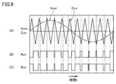
- FIGS. 9A, 9B and 9C are time charts showing waveforms of the AC voltage command value Vuvr, the carrier signal Cuv, and the gate signals Auv and Buv shown in FIG. 8A.
- the AC voltage command value Vuvr is a sine wave signal
- the carrier signal Cuv is a triangular wave signal.
- the cycle of the carrier signal Cuv is shorter than the cycle of the AC voltage command value Vuvr, and the amplitude of the carrier signal Cuv is larger than the amplitude of the AC voltage command value Vuvr.
- the gate signal Auv becomes “L” level, and the level of the carrier signal Cuv becomes AC voltage command.
- the gate signal Auv becomes “H” level.
- the gate signal Auv is a positive pulse signal train.
- the pulse width of the gate signal Auv is large during the period in which the AC voltage command value Vuvr is positive, and the pulse width of the gate signal Auv is small during the period in which the AC voltage command value Vuvr is negative.
- the gate signal Buv is an inverted signal of the gate signal Auv.
- the IGBTs 11 and 14 included in the corresponding inverter 10 are turned on and the IGBTs 12 and 13 are turned off.
- the positive terminal (positive DC line PL) of the capacitor 15 is connected to the AC terminal 5a via the IGBT 11
- the AC terminal 5b is connected to the negative terminal (negative) of the capacitor 15 via the IGBT 14.
- Side voltage line NL Side voltage line NL
- the terminal voltage of the capacitor 15 is output between the AC terminals 5a and 5b. That is, a positive DC voltage is output between the AC terminals 5a and 5b.
- the IGBTs 12 and 13 included in the corresponding inverter 10 are turned on and the IGBTs 11 and 14 are turned off.
- the positive terminal (positive DC line PL) of the capacitor 15 is connected to the AC terminal 5b via the IGBT 12
- the AC terminal 5a is connected to the negative terminal (negative DC line) of the capacitor 15 via the IGBT 13. NL)
- the inter-terminal voltage of the capacitor 15 is output between the AC terminals 5b and 5a. That is, a negative DC voltage is output between the AC terminals 5a and 5b.
- the waveforms of the AC voltage command value Vvwr, the carrier signal Cvw, and the gate signals Avw and Bvw shown in FIG. 8B, and the AC voltage command value Vur, the carrier signal Cwu, and the gate signal Awu shown in FIG. , Bwu waveforms are the same as those of AC voltage command value Vuvr, carrier signal Cuv, and gate signals Auv, Buv shown in FIGS. 9A to 9C, and description thereof will not be repeated.
- FIGS. 10A, 10B, and 10C are time charts showing the operation of the power conversion apparatus shown in FIGS.
- FIGS. 10A and 10B show the signals ⁇ 41 and ⁇ 46 of FIGS. 5A and 5B, respectively
- FIG. 10C shows the DC voltage VDC selected as the monitor voltage VM. .
- the power system 1 switches S1 to S3, transformer 2, switches S4 to S6, AC lines UL, VL, WL in FIG.
- the effective current flows to the capacitor 15 of each unit converter 5 through the reactors L1 to L3, and the DC voltage VDC of the capacitor 15 rises.
- d-axis current command value Idr for performing DC voltage control of inverter 10 is set to 0, and gate signal generating circuits 70, 80, 90 are inactivated. And the gate signals Auv, Buv, Avw, Bvw, Awu, Bwu are all fixed at the “L” level.
- q-axis current command value Iqr for performing reactive power control of inverter 10 is set to zero. That is, the DC voltage control and reactive power control of the inverter 10 are stopped, and the switching of the IGBTs 11 to 14 is stopped.
- the return level V2 and the protection level VH are set so that the DC voltage VDC does not exceed the protection level VH. Therefore, even if DC voltage VDC exceeds return level V2, DC voltage control and reactive power control are continued, DC voltage VDC gradually decreases, and DC voltage VDC again coincides with DC voltage command value VDCr at time t5.
- a dotted line in FIG. 10C indicates a change in the DC voltage VDC of the capacitor 15 in the first comparative example.
- the DC voltage control and reactive power control of the inverter 10 are stopped, and when the DC voltage VDC drops below the return level V2, the DC voltage control and invalidity are performed. Power control is resumed at the same time.
- the DC voltage control of the inverter 10 since the DC voltage control of the inverter 10 is resumed when the DC voltage VDC drops below the return level V1, the DC voltage VDC is rapidly reduced from the return level V1 to the return level V2. be able to. Therefore, in the present embodiment, even when an accident occurs in the power system 1, the operation of the inverter 10 can be restarted quickly, and the reactive power compensation can be restarted quickly.
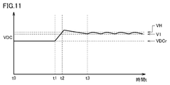
- FIG. 11 is a time chart showing the DC voltage VDC of the capacitor 15 in Comparative Example 2 of the present embodiment, which is compared with FIG. 10C.
- Comparative Example 2 when the DC voltage VDC exceeds the protection level VH (time t2), the DC voltage control and reactive power control of the inverter 10 are stopped, and when the DC voltage VDC drops below the return level V1 (time t3). ) Both DC voltage control and reactive power control are resumed.
- the reactive power control is restarted after the DC voltage VDC is lowered to the restoration level V2 that is sufficiently lower than the protection level VH by the DC voltage control. Does not vibrate between the protection level VH and the return level V1.
- FIG. 12 is a circuit diagram illustrating a main part of a power conversion device that is a third comparative example of the present embodiment.
- a resistance element 101 and a switch 102 are connected in series between the DC lines PL and NL of each unit converter.
- the switch 102 is normally turned off.
- Comparative Example 3 even when an accident occurs in the power system 1, the operation of the inverter 10 can be restarted quickly.
- the comparative example 3 it is necessary to provide the resistance element 101 and the switch 102 corresponding to each of the large number of capacitors 15, and there is a problem that the apparatus becomes large.
- the apparatus size since it is not necessary to provide the resistance element 101 and the switch 102, the apparatus size may be smaller than that of the comparative example 3.
- the apparatus can be reduced in size as compared with the case where the series connection body of the resistor element 101 and the switch 102 is connected in parallel to the capacitor 15.
- each of the arms A1 to A3 includes a plurality of unit converters 5
- each of the arms A1 to A3 includes only one unit converter 5. It can be applied to the case of inclusion.
- the return level V1 is set to a level lower than the protection level VH (V1 ⁇ VH).
- V1 VH
- 1 Power system 1u, 1v, 1w transmission line, S1 to S7,102 switch, 2,3 transformer, R1 to R3 current limiting resistor, UL, VL, WL AC line, C1 to C3 current transformer, L1 to L3 reactor, A1 to A3 arm, 4 control device, 5 unit converter, 5a, 5b AC terminal, 10, 74, 75, 84, 85, 94, 95 inverter, 11-14 IGBT, PL, NL DC line, 15 Capacitor, 16 voltage detector, 17 controller, 20 signal generator, 21 monitor voltage generator, 22-24, 72, 82, 92 comparator, 30 reactive power deviation calculator, 31 calculator, 32, 33 DQ conversion , 34 reactive power calculator, 35, 42, 51, 61 subtractor, 40 DC voltage controller, 41, 46 flip-flop, 43, 7 switching circuit, 44, 48, 52, 62 PI control unit, 45 reactive power control unit, 50, 60 current control unit, 53, 63 adder, 65 inverse DQ converter, 70, 80, 90 gate signal generation
Abstract
この電力変換装置では、電力系統(1)で事故が発生して単位変換器(5)に含まれるコンデンサ(15)の直流電圧(VDC)が保護レベル(VH)を超えた場合はインバータ(10)の運転を停止し、直流電圧(VDC)が復帰レベル(V1)以下に低下した場合はインバータ(10)の直流電圧制御を再開して直流電圧(VDC)を迅速に低下させ、直流電圧(VDC)が復帰レベル(V2)以下に低下した場合はインバータ(10)の無効電力制御を再開する。したがって、電力系統(1)で事故が発生した場合でも、インバータ(10)の運転を迅速に再開できる。
Description
この発明は電力変換装置に関し、特に、電力系統に結合される電力変換装置に関する。
国際公開2012/099176号明細書(特許文献1)には、MMCC(Modular Multilevel Cascade Converter)と呼ばれる電力変換装置が開示されている。この電力変換装置は、たとえば無効電力補償装置として使用され、デルタ接続された3個のアームを備える。各アームは、複数のコンデンサと、カスケード接続された複数のインバータとを含む。各インバータは、複数の半導体スイッチング素子を含み、対応するコンデンサと電力系統との間で電力を授受する。
このような電力変換装置では、電力系統で事故が発生して電力系統の電圧が上昇すると、電力系統からインバータを介してコンデンサに有効電流が流入し、コンデンサの直流電圧が許容レベルを超えてしまう場合がある。その場合にインバータを運転すると、サージ電圧が発生して半導体スイッチング素子が破壊されてしまう。
そこで、コンデンサの直流電圧が許容レベル以下の保護レベルを超えたときにインバータの運転を停止し、自然放電によってコンデンサの直流電圧が保護レベル以下の復帰レベルまで低下したときにインバータの運転を再開する方法が考えられる。しかし、この方法では、コンデンサの直流電圧を復帰レベルまで低下させるための時間が長くなり、インバータの停止時間が長くなるという問題がある。
その対策として、抵抗素子とスイッチとの直列接続体をコンデンサに並列接続し、コンデンサの直流電圧が保護レベルを超えたことに応じてスイッチをオンし、コンデンサから抵抗素子に電流を流し、コンデンサの直流電圧を迅速に低下させる方法が考えられる(図12参照)。
しかし、この方法では、コンデンサと同数の抵抗素子およびスイッチを設ける必要があり、装置寸法が大型化するという問題がある。
それゆえに、この発明の主たる目的は、電力系統で事故が発生した場合でも、インバータの運転を迅速に再開することが可能で小型の電力変換装置を提供することである。
この発明に係る電力変換装置は、コンデンサと、コンデンサと電力系統との間で電力を授受するインバータと、コンデンサの直流電圧が第1の指令値になるようにインバータの直流電圧制御を行なう第1の制御部と、コンデンサと電力系統の間で授受される無効電力が第2の指令値になるようにインバータの無効電力制御を行なう第2の制御部とを備えたものである。第1および第2の制御部は、直流電圧が第1の指令値よりも高い保護レベルを超えたことに応じて、それぞれ直流電圧制御および無効電力制御を停止する。第1の制御部は、直流電圧が保護レベル以下の第1の復帰レベル以下に低下したことに応じて直流電圧制御を再開する。第2の制御部は、直流電圧が第1の復帰レベルよりも低い第2の復帰レベル以下に低下したことに応じて無効電力制御を再開する。
この発明に係る電力変換装置では、コンデンサの直流電圧が保護レベルを超えたときにインバータの運転を停止し、直流電圧が第1の復帰レベル以下に低下したときにインバータの直流電圧制御のみを再開して直流電圧を迅速に低下させ、直流電圧が第2の復帰レベル以下に低下したときにインバータの無効電力制御を再開する。したがって、電力系統で事故が発生した場合でも、インバータの運転を迅速に再開することができる。また、抵抗素子およびスイッチの直列接続体をコンデンサに並列接続する場合に比べ、装置の小型化を図ることができる。
図1は、この発明の一実施の形態による電力変換装置の構成を示す回路ブロック図である。図1において、この電力変換装置は、電力系統1の無効電力を補償する無効電力補償装置として使用され、スイッチS1~S6、変圧器2,3、限流抵抗器R1~R3、交流ラインUL,VL,WL、変流器C1~C3、リアクトルL1~L3、アームA1~A3、および制御装置4を備える。
スイッチS1~S3の一方端子はそれぞれ電力系統1の三相の送電線1u,1v,1wに接続され、それらの他方端子はそれぞれ変圧器2の3つの一次巻線に接続される。スイッチS1~S3は、通常はオンされ、たとえば電力変換装置のメンテナンス時にオフされる。変圧器2は、3つの一次巻線と3つの二次巻線とを含み、三相交流電力を授受する。
限流抵抗器R1~R3の一方端子はそれぞれ変圧器2の3つの二次巻線に接続され、それらの他方端子はそれぞれ交流ラインUL,VL,WLの一方端子に接続される。限流抵抗器R1~R3は、電力変換装置の起動時に電力系統1からアームA1~A3に流れる電流を制限する。
スイッチS4~S6は、それぞれ限流抵抗器R1~R3に並列接続され、電力変換装置の起動時においてアームA1~A3に流れる電流が安定した後にオンされる。変圧器3は、交流ラインUL,VL,WLの交流電圧に応じた値の交流電圧Vu,Vv,Vwを制御装置4にフィードバックする。
リアクトルL1およびアームA1は、交流ラインULの他方端子と交流ラインVLの他方端子との間に直列接続される。リアクトルL2およびアームA2は、交流ラインVLの他方端子と交流ラインWLの他方端子との間に直列接続される。リアクトルL3およびアームA3は、交流ラインWLの他方端子と交流ラインULの他方端子との間に直列接続される。すなわち、アームA1~A3はデルタ接続されている。
リアクトルL1~L3は、アームA1~A3に流れる循環電流を抑制する。リアクトルL1~L3は、アームA1~A3とは別に設けられていてもよいし、アームA1~A3のインダクタンス成分であっても構わない。アームA1~A3は、制御装置4によって制御され、三相交流電力を発生する。変流器C1~C3は、それぞれアームA1~A3に流れる交流電流に応じた値の交流電流Iuv,Ivw,Iwuを制御装置4にフィードバックする。
アームA1~A3の各々は、カスケード接続された複数(たとえば20個)の単位変換器5を含む。複数の単位変換器5の各々は、制御装置4からの制御信号などに従って交流電力を発生する。
図2は、単位変換器5の構成を示す回路ブロック図である。図2において、単位変換器5は、交流端子5a,5b、スイッチS7、インバータ10、直流ラインPL,NL、コンデンサ15、電圧検出器16(第1の検出器)、および制御部17を含む。
アームA1~A3の初段の単位変換器5の交流端子5aは、それぞれ、リアクトルL1~L3を介して交流ラインUL,VL,WLの他方端子に接続される。アームA1~A3の最終段の単位変換器5の交流端子5bは、それぞれ交流ラインVL,WL,ULの他方端子に接続される。他の各単位変換器5の交流端子5aは前段の単位変換器5の交流端子5bに接続され、交流端子5bは次段の単位変換器5の交流端子5aに接続される。
スイッチS7は、交流端子5a,5b間に接続され、たとえば制御装置4によって制御される。スイッチS7は、対応する単位変換器5が正常である場合はオフされ、対応する単位変換器5が故障した場合はオンされる。スイッチS7がオンされると、交流端子5a,5b間が短絡され、対応する単位変換器5がバイパスされる。
インバータ10は、IGBT(Insulated Gate Bipolar Transistor)11~14およびダイオードD1~D4を含む。IGBT11,12のコレクタはともに正側の直流ラインPLに接続され、それらのエミッタはそれぞれ交流端子5a,5bに接続される。IGBT13,14のコレクタはそれぞれ交流端子5a,5bに接続され、それらのエミッタはともに負側の直流ラインNLに接続される。IGBT11~14の各々のゲートは、制御部17からのゲート信号を受ける。ダイオードD1~D4は、それぞれIGBT11~14に逆並列に接続される。
インバータ10は、制御装置4および制御部17によって直流電圧制御および無効電力制御され、電力系統1とコンデンサ15との間で電力を授受する。コンデンサ15は、直流ラインPL,NL間に接続され、直流電力を蓄える。電圧検出器16は、コンデンサ15の端子間の直流電圧に応じた値の直流電圧VDCを制御部17に出力する。
制御部17は、直流ラインPL,NLに接続され、コンデンサ15に蓄えられた直流電力によって駆動される。制御部17は、制御装置4からのゲート信号Auv,Buv,Avw,Bvw,Awu,Bwuに基づいてインバータ10を運転するとともに、電圧検出器16からの直流電圧VDCを示す信号を制御装置4に送信する。
図1に戻って、制御装置4は、無効電力指令値Qr、変圧器3からの交流電圧Vu,Vv,Vw、変流器C1~C3からの交流電流Iuv,Ivw,Iwu、各単位変換器5からの直流電圧VDCなどに基づいて、3つのアームA1~A3の各々(すなわち60個の単位変換器5の各々)を制御する。無効電力指令値Qrは、たとえば電力系統1の中央指令室から与えられる。電力変換装置は、無効電力指令値Qrに応じた値の無効電力を電力系統1に供給する。
図3は、制御装置4に含まれる信号発生回路20の構成を示す回路ブロック図である。図3において、信号発生回路20は、モニタ電圧生成部21および比較器22~24を含む。モニタ電圧生成部21は、60個の単位変換器5からの直流電圧VDCに基づいてモニタ電圧VMを生成する。モニタ電圧生成部21は、たとえば、60個の直流電圧VDCのうちの最も高い直流電圧VDCを選択し、選択した直流電圧VDCをモニタ電圧VMとして出力する。
比較器22は、モニタ電圧VMと保護レベルVHの高低を比較し、比較結果に基づいて保護信号Pを生成する。モニタ電圧VMが保護レベルVH以下の場合(VM≦VH)、保護信号Pは非活性化レベルの「H」レベルにされる。モニタ電圧VMが保護レベルVHよりも高い場合(VM>VH)、保護信号Pは活性化レベルの「L」レベルにされる。
保護レベルVHは、許容レベル以下で、直流電圧VDCの定格値および指令値よりも高い電圧である。電力系統1で事故が発生した場合、電力系統1からインバータ10を介してコンデンサ15に有効電流が流入し、コンデンサ15の直流電圧VDCが上昇して許容レベルを超える場合がある。
その場合に、インバータ10のIGBT11~14を駆動させると、サージ電圧が発生してIGBT11~14が破壊される恐れがある。そこで、この電力変換装置では、モニタ電圧VMが保護レベルVHを超えた場合は、保護信号Pを「H」レベルから「L」レベルに立ち下げて、全インバータ10の運転を停止させる。
比較器23は、モニタ電圧VMと復帰レベルV1(<VH)の高低を比較し、比較結果に基づいて復帰信号B1を生成する。モニタ電圧VMが復帰レベルV1よりも高い場合(VM>V1)、復帰信号B1は非活性化レベルの「H」レベルにされる。モニタ電圧VMが復帰レベルV1以下の場合(VM≦V1)、復帰信号B1は活性化レベルの「L」レベルにされる。
復帰レベルV1は、保護レベルVHよりも低く、直流電圧VDCの定格値および指令値よりも高い電圧である。電力系統1が事故から正常に復帰した後は、電力変換装置の運転を迅速に再開する必要がある。しかし、コンデンサ15の直流電圧VDCが保護レベルVH以下になったときに直ぐにインバータ10の無効電力制御を再開すると、電力変換装置から電力系統1に無効電力が供給されて電力系統1の電圧が上昇し、コンデンサ15の直流電圧VDCが再度、上昇して保護レベルVHを超えてしまう。その結果、インバータ10の運転と停止が繰り返され、電力変換装置が正常に動作しなくなってしまう。
そこで、この電力変換装置では、インバータ10の運転が停止されている場合にモニタ電圧VMが復帰レベルV1以下に低下したときには、復帰信号B1を「H」レベルから「L」レベルに立ち下げて、インバータ10の直流電圧制御のみを再開させる。これにより、電力系統1の電圧を上昇させることなく、コンデンサ15の直流電圧VDCを迅速に低下させることが可能となる。
比較器24は、モニタ電圧VMと復帰レベルV2(<V1)の高低を比較し、比較結果に基づいて復帰信号B2を生成する。モニタ電圧VMが復帰レベルV2よりも高い場合(VM>V2)、復帰信号B2は非活性化レベルの「H」レベルにされる。モニタ電圧VMが復帰レベルV2以下の場合(VM≦V2)、復帰信号B2は活性化レベルの「L」レベルにされる。
復帰レベルV2は、復帰レベルV1よりも低く、直流電圧VDCの定格値および指令値よりも高い電圧である。復帰レベルV2は、インバータ10の無効電力制御を再開したために電力系統1の電圧が上昇し、コンデンサ15の直流電圧VDCが再度、上昇したとしても、直流電圧VDCが保護レベルVHを超える恐れがないような値に設定される。
したがって、モニタ電圧VMが復帰レベルV2以下に低下した場合には、インバータ10の直流電圧制御および無効電力制御が再開され、電力変換装置の運転が定常状態に復帰される。
図4は、制御装置4に含まれる無効電力偏差演算部30の構成を示すブロック図である。図4において、無効電力偏差演算部30は、演算器31、DQ変換器32,33、無効電力演算器34、および減算器35を含む。
演算器31は、変流器C1~C3からの交流電流Iuv,Ivw,Iwuに基づいて、交流ラインUL,VL,WLに流れる交流電流に応じたレベルの交流電流Iu,Iv,Iwを求める。
DQ変換器32は、三相交流電流Iu,Iv,Iwをd軸電流Idおよびq軸電流Iqに変換する。DQ変換器33は、変圧器3からの三相交流電圧Vu,Vv,Vwをd軸電圧Vdおよびq軸電圧Vqに変換する。無効電力演算器34は、d軸電流Id、q軸電流Iq、d軸電圧Vd、およびq軸電圧Vqに基づいて無効電力Qを求める。減算器35は、無効電力指令値Qrと無効電力Qの偏差ΔQ=Qr-Qを求める。
制御装置4は、さらに、60個の単位変換器5に対応する直流電圧指令値VDCrを生成する。直流電圧指令値VDCrは、60個の単位変換器5に与えられる。直流電圧指令値VDCrは通常、定格直流電圧に設定される。
図5(A),(B)は、直流電圧制御部40および無効電力制御部45の構成を示すブロック図である。直流電圧制御部40は、図5(A)に示すように、フリップフロップ41、減算器42、切換回路43、およびPI(Proportional Integral)制御部44を含む。直流電圧制御部40は、コンデンサ15の直流電圧VDCが直流電圧指令値VDCrになるようにインバータ10の直流電圧制御を行なう第1の制御部を構成する。
フリップフロップ41は、保護信号Pおよび復帰信号B1がともに「H」レベルである場合はリセットされ、出力信号φ41を「L」レベル(0)にする。フリップフロップ41は、保護信号Pが「H」レベルから「L」レベルに立ち下げられるとセットされ、出力信号φ41を「L」レベル(0)から「H」レベル(1)に立ち上げる。信号φ41は、切換回路43およびPI制御部44の各々に与えられる。
減算器42は、直流電圧指令値VDCrと直流電圧VDCの偏差ΔVDC=VDCr-VDCを求める。切換回路43は、信号φ41が「L」レベル(0)である場合は減算器42からの偏差ΔVDCをPI制御部44に与え、信号φ41が「H」レベル(1)である場合は「0」をPI制御部44に与える。
PI制御部44は、切換回路43の出力値(ΔVDCまたは0)に比例した値と出力値を積分した値とを加算してd軸電流指令値Idrを生成する。信号φ41が「L」レベル(0)である場合、PI制御部44は、切換回路43からの偏差ΔVDCに比例した値と偏差ΔVDCを積分した値とを加算してd軸電流指令値Idrを生成し、インバータ10の直流電圧制御を行なう。
信号φ41が「H」レベル(1)である場合、PI制御部44における積分値は0にリセットされ、d軸電流指令値Idrは0に固定され、インバータ10の直流電圧制御が停止される。信号φ41が「H」レベル(1)から「L」レベル(0)に変化すると、インバータ10の直流電圧制御が再開される。
無効電力制御部45は、図5(B)に示すように、フリップフロップ46、切換回路47、およびPI制御部48を含む。無効電力制御部45と図4の無効電力偏差演算部30とは、コンデンサ15と電力系統1の間で授受される無効電力Qが無効電力指令値Qrになるようにインバータ10の無効電力制御を行なう第2の制御部を構成する。
フリップフロップ46は、保護信号Pおよび復帰信号B2がともに「H」レベルである場合はリセットされ、出力信号φ46を「L」レベル(0)にする。フリップフロップ46は、保護信号Pが「H」レベルから「L」レベルに立ち下げられるとセットされ、出力信号φ46を「L」レベル(0)から「H」レベル(1)に立ち上げる。信号φ46は、切換回路47およびPI制御部48の各々に与えられる。
切換回路47は、信号φ46が「L」レベル(0)である場合は制御装置4からの無効電力偏差ΔQをPI制御部48に与え、信号φ46が「H」レベル(1)である場合は「0」をPI制御部48に与える。
PI制御部48は、切換回路47の出力値(ΔQまたは0)に比例した値と出力値を積分した値とを加算してq軸電流指令値Iqrを生成する。信号φ46が「L」レベル(0)である場合、PI制御部48は、切換回路47からの偏差ΔQに比例した値と偏差ΔQを積分した値とを加算してq軸電流指令値Iqrを生成し、インバータ10の無効電力制御を行なう。
信号φ46が「H」レベル(1)である場合、PI制御部48における積分値は0にリセットされ、q軸電流指令値Iqrは0に固定され、インバータ10の無効電力制御が停止される。信号φ46が「H」レベル(1)から「L」レベル(0)に変化すると、インバータ10の無効電力制御が再開される。
図6(A),(B)は、電流制御部50,60の構成を示すブロック図である。電流制御部50は、図6(A)に示すように、減算器51、PI制御部52、および加算器53を含む。減算器51は、直流電圧制御部40(図5(A))からのd軸電流指令値IdrとDQ変換器32(図4)からのd軸電流Idとの偏差ΔId=Idr-Idを求める。
PI制御部52は、フリップフロップ41(図5(A))の出力信号φ41によって制御される。信号φ41が「L」レベル(0)である場合、PI制御部52は、偏差ΔIdに比例した値と偏差ΔIdを積分した値とを加算してd軸電圧Vd1を生成する。信号φ41が「H」レベル(1)である場合、PI制御部52における積分値は0にリセットされ、d軸電圧Vd1は0に固定される。加算器53は、PI制御部52からのd軸電圧Vd1にDQ変換器33からのd軸電圧Vdを加算してd軸電圧指令値Vdrを生成する。
電流制御部60は、図6(B)に示すように、減算器61、PI制御部62、および加算器63を含む。減算器61は、無効電力制御部45(図5(A))からのq軸電流指令値IqrとDQ変換器32(図4)からのq軸電流Iqとの偏差ΔIq=Iqr-Iqを求める。
PI制御部62は、フリップフロップ41の出力信号φ41によって制御される。信号φ41が「L」レベル(0)である場合、PI制御部62は、偏差ΔIqに比例した値と偏差ΔIqを積分した値とを加算してq軸電圧Vq1を生成する。信号φ41が「H」レベル(1)である場合、PI制御部62における積分値は0にリセットされ、q軸電圧Vq1は0に固定される。加算器63は、PI制御部62からのq軸電圧Vq1にDQ変換器33からのq軸電圧Vqを加算してq軸電圧指令値Vqrを生成する。
図7は、逆DQ変換器65の構成を示すブロック図である。図7において、逆DQ変換器65は、電流制御部50,60からのd軸電圧指令値Vdrおよびq軸電圧指令値Vqrを逆DQ変換して三相交流電圧指令値Vuvr,Vvwr,Vwurに変換する。三相交流電圧指令値Vuvr,Vvwr,Vwurの各々は正弦波であり、三相交流電圧指令値Vuvr,Vvwr,Vwurの位相は120度ずつずれている。
図8(A),(B),(C)は、ゲート信号発生回路70,80,90の構成を示す回路図である。ゲート信号発生回路70は、図8(A)に示すように、比較器72、バッファ73、インバータ74,75、およびANDゲート76,77を含む。
比較器72は、交流電圧指令値Vuvrのレベルとキャリア信号Cuvのレベルとの高低を比較し、比較結果に応じたレベルの信号φ72を出力する。キャリア信号Cuvは、交流電圧指令値Vuvrよりも高い周波数を有し、交流電圧指令値Vuvrに同期した三角波信号である。
Vuvr>Cuvである場合は信号φ72は「H」レベルとなり、Vuvr<Cuvである場合は信号φ72は「L」レベルとなる。バッファ73は、信号φ72をANDゲート76の一方入力ノードに与える。インバータ74は、信号φ72を反転させてANDゲート77の一方入力ノードに与える。インバータ75は、フリップフロップ41(図5(A))の出力信号φ41を反転させてANDゲート76,77の他方入力ノードに与える。ANDゲート76,77の出力信号は、それぞれゲート信号Auv,Buvとなる。
信号φ41が「L」レベルである場合は、比較器72の出力信号φ72がバッファ73およびANDゲート76を通過してゲート信号Auvとなるとともに、比較器72の出力信号φ72がインバータ74によって反転され、ANDゲート77を通過してゲート信号Buvとなる。信号φ41が「H」レベルである場合は、ANDゲート76,77の出力信号であるゲート信号Auv,Buvはともに「L」レベルに固定される。
ゲート信号Auvは対応のインバータ10に含まれるIGBT11,14の各々のゲートに与えられ、ゲート信号Buvは対応のインバータ10に含まれるIGBT12,13の各々のゲートに与えられる。信号φ41が「L」レベルである場合は、ゲート信号Auv,Buvによって対応のインバータ10が運転される。信号φ41が「H」レベルである場合は、ゲート信号Auv,Buvが「L」レベルに固定されて対応のインバータ10の運転が停止される。
ゲート信号発生回路80は、図8(B)に示すように、比較器82、バッファ83、インバータ84,85、およびANDゲート86,87を含む。比較器82は、交流電圧指令値Vvwrのレベルとキャリア信号Cvwのレベルとの高低を比較し、比較結果に応じたレベルの信号φ82を出力する。キャリア信号Cvwは、交流電圧指令値Vvwrよりも高い周波数を有し、交流電圧指令値Vvwrに同期した三角波信号である。
Vvwr>Cvwである場合は信号φ82は「H」レベルとなり、Vvwr<Cvwである場合は信号φ82は「L」レベルとなる。バッファ83は、信号φ82をANDゲート86の一方入力ノードに与える。インバータ84は、信号φ82を反転させてANDゲート87の一方入力ノードに与える。インバータ85は、フリップフロップ41(図5(A))の出力信号φ41を反転させてANDゲート86,87の他方入力ノードに与える。ANDゲート86,87の出力信号は、それぞれゲート信号Avw,Bvwとなる。
信号φ41が「L」レベルである場合は、比較器82の出力信号φ82がバッファ83およびANDゲート86を通過してゲート信号Avwとなるとともに、比較器82の出力信号φ82がインバータ84によって反転され、ANDゲート87を通過してゲート信号Bvwとなる。信号φ41が「H」レベルである場合は、ANDゲート86,87の出力信号であるゲート信号Avw,Bvwはともに「L」レベルに固定される。
ゲート信号Avwは対応のインバータ10に含まれるIGBT11,14の各々のゲートに与えられ、ゲート信号Bvwは対応のインバータ10に含まれるIGBT12,13の各々のゲートに与えられる。信号φ41が「L」レベルである場合は、ゲート信号Avw,Bvwによって対応のインバータ10が運転される。信号φ41が「H」レベルである場合は、ゲート信号Avw,Bvwが「L」レベルに固定されて対応のインバータ10の運転が停止される。
ゲート信号発生回路90は、図8(C)に示すように、比較器92、バッファ93、インバータ94,95、およびANDゲート96,97を含む。比較器92は、交流電圧指令値Vwurのレベルとキャリア信号Cwuのレベルとの高低を比較し、比較結果に応じたレベルの信号φ92を出力する。キャリア信号Cwuは、交流電圧指令値Vwurよりも高い周波数を有し、交流電圧指令値Vwurに同期した三角波信号である。
Vwur>Cwuである場合は信号φ92は「H」レベルとなり、Vwur<Cwuである場合は信号φ92は「L」レベルとなる。バッファ93は、信号φ92をANDゲート96の一方入力ノードに与える。インバータ94は、信号φ92を反転させてANDゲート97の一方入力ノードに与える。インバータ95は、フリップフロップ41(図5(A))の出力信号φ41を反転させてANDゲート96,97の他方入力ノードに与える。ANDゲート96,97の出力信号は、それぞれゲート信号Awu,Bwuとなる。
信号φ41が「L」レベルである場合は、比較器92の出力信号φ92がバッファ93およびANDゲート96を通過してゲート信号Awuとなるとともに、比較器92の出力信号φ92がインバータ94によって反転され、ANDゲート97を通過してゲート信号Bwuとなる。信号φ41が「H」レベルである場合は、ANDゲート96,97の出力信号であるゲート信号Awu,Bwuはともに「L」レベルに固定される。
ゲート信号Awuは対応のインバータ10に含まれるIGBT11,14の各々のゲートに与えられ、ゲート信号Bwuは対応のインバータ10に含まれるIGBT12,13の各々のゲートに与えられる。信号φ41が「L」レベルである場合は、ゲート信号Awu,Bwuによって対応のインバータ10が運転される。信号φ41が「H」レベルである場合は、ゲート信号Awu,Bwuが「L」レベルに固定されて対応のインバータ10の運転が停止される。
図9(A),(B),(C)は、図8(A)に示した交流電圧指令値Vuvr、キャリア信号Cuv、およびゲート信号Auv,Buvの波形を示すタイムチャートである。図9(A)に示すように、交流電圧指令値Vuvrは正弦波信号であり、キャリア信号Cuvは三角波信号である。キャリア信号Cuvの周期は交流電圧指令値Vuvrの周期よりも短く、キャリア信号Cuvの振幅は交流電圧指令値Vuvrの振幅よりも大きい。
図9(A),(B)に示すように、キャリア信号Cuvのレベルが交流電圧指令値Vuvrよりも高い場合はゲート信号Auvは「L」レベルになり、キャリア信号Cuvのレベルが交流電圧指令値Vuvrよりも低い場合はゲート信号Auvは「H」レベルになる。ゲート信号Auvは、正パルス信号列となる。交流電圧指令値Vuvrが正極性である期間ではゲート信号Auvのパルス幅は大きく、交流電圧指令値Vuvrが負極性である期間ではゲート信号Auvのパルス幅は小さい。図9(B),(C)に示すように、ゲート信号Buvはゲート信号Auvの反転信号となる。
ゲート信号Auv,Buvがそれぞれ「H」レベルおよび「L」レベルである場合は、対応のインバータ10に含まれるIGBT11,14がオンするとともにIGBT12,13がオフする。この場合は図2において、コンデンサ15の正側端子(正側直流ラインPL)がIGBT11を介して交流端子5aに接続されるとともに、交流端子5bがIGBT14を介してコンデンサ15の負側端子(負側直流ラインNL)に接続され、交流端子5a,5b間にコンデンサ15の端子間電圧が出力される。すなわち、交流端子5a,5b間に正の直流電圧が出力される。
ゲート信号Auv,Buvがそれぞれ「L」レベルおよび「H」レベルである場合は、対応のインバータ10に含まれるIGBT12,13がオンするとともにIGBT11,14がオフする。この場合は、コンデンサ15の正側端子(正側直流ラインPL)がIGBT12を介して交流端子5bに接続されるとともに、交流端子5aがIGBT13を介してコンデンサ15の負側端子(負側直流ラインNL)に接続され、交流端子5b,5a間にコンデンサ15の端子間電圧が出力される。すなわち、交流端子5a,5b間に負の直流電圧が出力される。
図9(B),(C)に示すようにゲート信号Auv,Buvの波形が変化すると、図9(A)に示した交流電圧指令値Vuvrと同じ位相の交流電圧が交流端子5a,5b間に出力される。アームA1では20個の単位変換器5がカスケード接続されているので、20個の単位変換器5の交流端子5a,5b間に現れる交流電圧を加算した値の交流電圧がアームA1の端子間に現れる。
図8(B)に示した交流電圧指令値Vvwr、キャリア信号Cvw、およびゲート信号Avw,Bvwの波形と、図8(C)に示した交流電圧指令値Vwur、キャリア信号Cwu、およびゲート信号Awu,Bwuの波形とについては、図9(A)~(C)に示した交流電圧指令値Vuvr、キャリア信号Cuv、およびゲート信号Auv,Buvの波形と同様であるので、その説明は繰り返さない。
図10(A),(B),(C)は、図1~図9に示した電力変換装置の動作を示すタイムチャートである。特に、図10(A),(B)はそれぞれ図5(A),(B)の信号φ41,φ46を示し、図10(C)はモニタ電圧VMとして選択された直流電圧VDCを示している。
図10(A)~(C)において、初期状態(時刻t0)では電力系統1は正常であり、インバータ10の無効電力制御および直流電圧制御が実行され、直流電圧VDCは直流電圧指令値VDCrに一致しており、信号φ41,φ46はともに「L」レベル(0)であるものとする。
ある時刻t1において電力系統1で事故が発生して電力系統1の電圧が上昇すると、図1において電力系統1からスイッチS1~S3、変圧器2、スイッチS4~S6、交流ラインUL,VL,WL、リアクトルL1~L3を介して各単位変換器5のコンデンサ15に有効電流が流れ、コンデンサ15の直流電圧VDCが上昇する。
直流電圧VDCが復帰レベルV2、復帰レベルV1、および保護レベルVHを超えると、図3において復帰信号B2,B1および保護信号Pが「H」レベルから「L」レベルに立ち下げられる。保護信号Pが「H」レベルから「L」レベルに立ち下げられると、図5(A),(B)においてフリップフロップ41,46がセットされ、信号φ41,φ46がともに「H」レベル(1)に立ち上げられる。
信号φ41が「H」レベル(1)にされると、インバータ10の直流電圧制御を行なうためのd軸電流指令値Idrが0に設定され、さらにゲート信号発生回路70,80,90が非活性化されてゲート信号Auv,Buv,Avw,Bvw,Awu,Bwuがともに「L」レベルに固定される。信号φ46が「H」レベル(1)に設定されると、インバータ10の無効電力制御を行なうためのq軸電流指令値Iqrが0に設定される。すなわち、インバータ10の直流電圧制御および無効電力制御が停止され、IGBT11~14のスイッチングが停止される。
電力系統1が正常に復帰すると、コンデンサ15の電荷が制御部17によって消費されたり、自然放電され、コンデンサ15の直流電圧VDCが徐々に低下する。直流電圧VDCが保護レベルVH以下に低下すると保護信号Pが「L」レベルから「H」レベルに立ち上げられる。
時刻t3において直流電圧VDCが復帰レベルV1以下に低下すると復帰信号B1が「L」レベルから「H」レベルに立ち上げられる。復帰信号B1が「H」レベルに立ち上げられると、図5(A)のフリップフロップ41がリセットされて信号φ41が「L」レベル(0)に立ち下げられる。
信号φ41が「L」レベル(0)にされると、直流電圧指令値VDCrと直流電圧VDCの偏差ΔVDCが切換回路43を介してPI制御部44に与えられるとともに、PI制御部44が活性化され、さらにゲート信号発生回路70,80,90が活性化されて、インバータ10の直流電圧制御が再開される。これにより、直流電圧VDCは直流電圧指令値VDCrに向かって迅速に低下する。なお、直流電圧制御による電力系統1の電圧変動は少ない。
時刻t4において直流電圧VDCが復帰レベルV2以下に低下すると、復帰信号B2が「L」レベルから「H」レベルに立ち上げられる。復帰信号B2が「H」レベルに立ち上げられると、図5(B)のフリップフロップ46がリセットされて信号φ46が「L」レベル(0)に立ち下げられる。
信号φ46が「L」レベル(0)にされると、無効電力偏差ΔQが切換回路47を介してPI制御部48に与えられるとともに、PI制御部48が活性化され、インバータ10の無効電力制御が再開される。無効電力制御が再開されると、電力系統1の電圧が少し上昇し、電力系統1からコンデンサ15に有効電流が流入し、直流電圧VDCが少し上昇する。
このとき直流電圧VDCが保護レベルVHを超えないように、復帰レベルV2および保護レベルVHが設定されている。したがって、直流電圧VDCが復帰レベルV2を超えても直流電圧制御および無効電力制御が継続され、直流電圧VDCが徐々に低下し、時刻t5において直流電圧VDCが直流電圧指令値VDCrに再び一致する。
[比較例1]
図10(C)の点線は、比較例1におけるコンデンサ15の直流電圧VDCの変化を示している。この比較例1では、直流電圧VDCが保護レベルVHを超えたときにインバータ10の直流電圧制御および無効電力制御が停止され、直流電圧VDCが復帰レベルV2以下に低下したときに直流電圧制御および無効電力制御が同時に再開される。
図10(C)の点線は、比較例1におけるコンデンサ15の直流電圧VDCの変化を示している。この比較例1では、直流電圧VDCが保護レベルVHを超えたときにインバータ10の直流電圧制御および無効電力制御が停止され、直流電圧VDCが復帰レベルV2以下に低下したときに直流電圧制御および無効電力制御が同時に再開される。
時刻t0~t3において本願発明の直流電圧VDCと比較例1の直流電圧VDCは同様に変化したものとする。比較例1では、時刻t3を過ぎた後も自然放電および制御部17によってコンデンサ15の電荷を消費させるだけであるので、直流電圧VDCを復帰レベルV1から復帰レベルV2まで低下させるために必要な時間が長くなる。したがって、比較例1では、電力系統1で事故が発生してからインバータ10の運転を再開するまでの時間が長くなる。
これに対して本実施の形態では、直流電圧VDCが復帰レベルV1以下に低下したときにインバータ10の直流電圧制御を再開するので、直流電圧VDCを復帰レベルV1から復帰レベルV2まで迅速に低下させることができる。したがって、本実施の形態では、電力系統1で事故が発生した場合でも、インバータ10の運転を迅速に再開することができ、無効電力補償を迅速に再開することができる。
[比較例2]
図11は、本実施の形態の比較例2におけるコンデンサ15の直流電圧VDCを示すタイムチャートであって、図10(C)と対比される図である。比較例2では、直流電圧VDCが保護レベルVHを超えたとき(時刻t2)にインバータ10の直流電圧制御および無効電力制御が停止され、直流電圧VDCが復帰レベルV1以下に低下したとき(時刻t3)に直流電圧制御および無効電力制御がともに再開される。
図11は、本実施の形態の比較例2におけるコンデンサ15の直流電圧VDCを示すタイムチャートであって、図10(C)と対比される図である。比較例2では、直流電圧VDCが保護レベルVHを超えたとき(時刻t2)にインバータ10の直流電圧制御および無効電力制御が停止され、直流電圧VDCが復帰レベルV1以下に低下したとき(時刻t3)に直流電圧制御および無効電力制御がともに再開される。
時刻t0~t3において本願発明の直流電圧VDCと比較例2の直流電圧VDCは同様に変化したものとする。時刻t3において直流電圧制御および無効電力制御を再開すると、無効電力によって電力系統1の電圧が上昇し、電力系統1からコンデンサ15に有効電流が流入し、直流電圧VDCが上昇する。保護レベルVHと復帰レベルV1の差が小さいので、直流電圧VDCが保護レベルVHを超え、直流電圧制御および無効電力制御が再び停止される。以降、同様の動作が繰り返され、直流電圧VDCが保護レベルVHと復帰レベルV1の間で振動し、直流電圧VDCは直流電圧指令値VDCrに一致しなくなる。
これに対して本願発明では、直流電圧制御によって直流電圧VDCを保護レベルVHよりも十分に低い復帰レベルV2以下に低下させた後に無効電力制御を再開するので、比較例2のように直流電圧VDCが保護レベルVHと復帰レベルV1の間で振動することはない。
[比較例3]
図12は、本実施の形態の比較例3となる電力変換装置の要部を示す回路図である。図12において、この比較例3では、各単位変換器の直流ラインPL,NL間に抵抗素子101およびスイッチ102が直列接続される。スイッチ102は、通常はオフされている。
図12は、本実施の形態の比較例3となる電力変換装置の要部を示す回路図である。図12において、この比較例3では、各単位変換器の直流ラインPL,NL間に抵抗素子101およびスイッチ102が直列接続される。スイッチ102は、通常はオフされている。
電力系統1で事故が発生してコンデンサ15の直流電圧VDCが保護レベルVHを超えた場合は、インバータ10の運転が停止されるとともにスイッチ102がオンされる。スイッチ102がオンされると、コンデンサ15から抵抗素子101に電流が流れ、直流電圧VDCが迅速に低下する。直流電圧VDCが復帰レベルV2以下に低下した場合は、スイッチ102がオフされ、インバータ10の直流電圧制御および無効電力制御が再開される。
この比較例3では、電力系統1で事故が発生した場合でも、インバータ10の運転を迅速に再開することができる。しかし、この比較例3では、多数のコンデンサ15の各々に対応して抵抗素子101およびスイッチ102を設ける必要があり、装置が大型化するという問題がある。これに対して本実施の形態では、抵抗素子101およびスイッチ102を設ける必要がないので、比較例3と比べ装置寸法が小さくて済む。
以上のように、本実施の形態では、コンデンサ15の直流電圧VDCが保護レベルVHを超えた場合はインバータ10の運転を停止し、直流電圧VDCが復帰レベルV1以下に低下した場合はインバータ10の直流電圧制御を再開して直流電圧VDCを低下させ、直流電圧VDCが復帰レベルV2以下に低下した場合はインバータ10の無効電力制御を再開する。したがって、電力系統1で事故が発生した場合でも、インバータ10の運転を迅速に再開することができる。また、抵抗素子101およびスイッチ102の直列接続体をコンデンサ15に並列接続する場合に比べ、装置の小型化を図ることができる。
なお、本実施の形態では、アームA1~A3の各々が複数段の単位変換器5を含む場合について説明したが、本願発明は、アームA1~A3の各々が1段の単位変換器5のみを含む場合にも適用することができる。
また、本実施の形態では、復帰レベルV1を保護レベルVHよりも低いレベルに設定した場合(V1<VH)について説明したが、復帰レベルV1を保護レベルVHと同レベルに設定してもよい(V1=VH)。ただし、この場合はインバータ10の直流電圧制御を再開して直流電圧VDCが若干変動したときに、直流電圧VDCが再度、保護レベルVHを超え、インバータ10の運転が停止される恐れがある。
今回開示された実施の形態はすべての点で例示であって制限的なものではないと考えられるべきである。本発明の範囲は上記した説明ではなくて請求の範囲によって示され、請求の範囲と均等の意味および範囲内でのすべての変更が含まれることが意図される。
1 電力系統、1u,1v,1w 送電線、S1~S7,102 スイッチ、2,3 変圧器、R1~R3 限流抵抗器、UL,VL,WL 交流ライン、C1~C3 変流器、L1~L3 リアクトル、A1~A3 アーム、4 制御装置、5 単位変換器、5a,5b 交流端子、10,74,75,84,85,94,95 インバータ、11~14 IGBT、PL,NL 直流ライン、15 コンデンサ、16 電圧検出器、17 制御部、20 信号発生回路、21 モニタ電圧生成部、22~24,72,82,92 比較器、30 無効電力偏差演算部、31 演算器、32,33 DQ変換器、34 無効電力演算器、35,42,51,61 減算器、40 直流電圧制御部、41,46 フリップフロップ、43,47 切換回路、44,48,52,62 PI制御部、45 無効電力制御部、50,60 電流制御部、53,63 加算器、65 逆DQ変換器、70,80,90 ゲート信号発生回路、73,83,93 バッファ、76,77,86,87,96,97 ANDゲート、101 抵抗素子。
Claims (8)
- コンデンサと、
前記コンデンサと電力系統との間で電力を授受するインバータと、
前記コンデンサの直流電圧が第1の指令値になるように前記インバータの直流電圧制御を行なう第1の制御部と、
前記コンデンサと前記電力系統の間で授受される無効電力が第2の指令値になるように前記インバータの無効電力制御を行なう第2の制御部とを備え、
前記第1および第2の制御部は、前記直流電圧が前記第1の指令値よりも高い保護レベルを超えたことに応じて、それぞれ前記直流電圧制御および前記無効電力制御を停止し、
前記第1の制御部は、前記直流電圧が前記保護レベル以下の第1の復帰レベル以下に低下したことに応じて前記直流電圧制御を再開し、
前記第2の制御部は、前記直流電圧が前記第1の復帰レベルよりも低い第2の復帰レベル以下に低下したことに応じて前記無効電力制御を再開する、電力変換装置。 - 前記電力系統に事故が発生して前記電力系統から前記インバータを介して前記コンデンサに電流が流入すると前記直流電圧が上昇し、
前記直流電圧が前記保護レベルよりも高い許容レベルを超えた場合に前記インバータを運転すると前記インバータが破壊される、請求項1に記載の電力変換装置。 - さらに、前記直流電圧を検出する第1の検出器と、
前記無効電力を検出する第2の検出器とを備え、
前記第1の制御部は、前記第1の検出器の検出結果に基づいて前記直流電圧制御を行ない、
前記第2の制御部は、前記第2の検出器の検出結果に基づいて前記無効電力制御を行なう、請求項1に記載の電力変換装置。 - さらに、前記直流電圧が前記保護レベルを超えたことに応じて保護信号を出力し、前記直流電圧が前記第1の復帰レベル以下に低下したことに応じて第1の復帰信号を出力し、前記直流電圧が前記第2の復帰レベル以下に低下したことに応じて第2の復帰信号を出力する信号発生回路を備え、
前記第1および第2の制御部は、前記保護信号に応答して、それぞれ前記直流電圧制御および前記無効電力制御を停止し、
前記第1の制御部は、前記第1の復帰信号に応答して前記直流電圧制御を再開し、
前記第2の制御部は、前記第2の復帰信号に応答して前記無効電力制御を再開する、請求項1に記載の電力変換装置。 - 各々が前記コンデンサおよび前記インバータを含む複数の単位変換器を備え、
前記複数の単位変換器に含まれる複数の前記インバータはカスケード接続され、
前記第1の制御部は対応する前記インバータの前記直流電圧制御を行ない、
前記第2の制御部は対応する前記インバータの前記無効電力制御を行なう、請求項1に記載の電力変換装置。 - さらに、複数の前記直流電圧のうちのいずれかの直流電圧が前記保護レベルを超えたことに応じて保護信号を出力し、当該直流電圧が前記第1の復帰レベル以下に低下したことに応じて第1の復帰信号を出力し、当該直流電圧が前記第2の復帰レベル以下に低下したことに応じて第2の復帰信号を出力する信号発生回路を備え、
前記第1の制御部は、前記保護信号に応答して、対応する前記インバータの前記直流電圧制御を停止し、
前記第2の制御部は、前記保護信号に応答して、対応する前記インバータの前記無効電力制御を停止し、
前記第1の制御部は、前記第1の復帰信号に応答して、対応する前記インバータの前記直流電圧制御を再開し、
前記第2の制御部は、前記第2の復帰信号に応答して、対応する前記インバータの前記無効電力制御を再開する、請求項5に記載の電力変換装置。 - 各々が前記複数の単位変換器を含む3個のアームを備え、
前記3個のアームはデルタ接続されている、請求項5に記載の電力変換装置。 - 前記電力変換装置は、前記電力系統の無効電力を補償する無効電力補償装置として使用される、請求項7に記載の電力変換装置。
Priority Applications (4)
| Application Number | Priority Date | Filing Date | Title |
|---|---|---|---|
| JP2019506789A JP6748290B2 (ja) | 2017-03-22 | 2017-03-22 | 電力変換装置 |
| PCT/JP2017/011405 WO2018173144A1 (ja) | 2017-03-22 | 2017-03-22 | 電力変換装置 |
| EP17901397.4A EP3605822B1 (en) | 2017-03-22 | 2017-03-22 | Power conversion device |
| US16/494,923 US10826383B2 (en) | 2017-03-22 | 2017-03-22 | Power conversion device |
Applications Claiming Priority (1)
| Application Number | Priority Date | Filing Date | Title |
|---|---|---|---|
| PCT/JP2017/011405 WO2018173144A1 (ja) | 2017-03-22 | 2017-03-22 | 電力変換装置 |
Publications (1)
| Publication Number | Publication Date |
|---|---|
| WO2018173144A1 true WO2018173144A1 (ja) | 2018-09-27 |
Family
ID=63585083
Family Applications (1)
| Application Number | Title | Priority Date | Filing Date |
|---|---|---|---|
| PCT/JP2017/011405 WO2018173144A1 (ja) | 2017-03-22 | 2017-03-22 | 電力変換装置 |
Country Status (4)
| Country | Link |
|---|---|
| US (1) | US10826383B2 (ja) |
| EP (1) | EP3605822B1 (ja) |
| JP (1) | JP6748290B2 (ja) |
| WO (1) | WO2018173144A1 (ja) |
Cited By (1)
| Publication number | Priority date | Publication date | Assignee | Title |
|---|---|---|---|---|
| WO2021166164A1 (ja) * | 2020-02-20 | 2021-08-26 | 三菱電機株式会社 | 電力変換装置および航空機の電力システム |
Families Citing this family (1)
| Publication number | Priority date | Publication date | Assignee | Title |
|---|---|---|---|---|
| EP3637573B1 (en) * | 2017-06-08 | 2021-06-02 | Mitsubishi Electric Corporation | Power control system and control device |
Citations (4)
| Publication number | Priority date | Publication date | Assignee | Title |
|---|---|---|---|---|
| JP2002281670A (ja) * | 2001-03-19 | 2002-09-27 | Mitsubishi Electric Corp | 電力変換装置 |
| WO2012099176A1 (ja) | 2011-01-18 | 2012-07-26 | 国立大学法人東京工業大学 | 電力変換器およびその制御方法 |
| JP2016100926A (ja) * | 2014-11-19 | 2016-05-30 | 三菱電機株式会社 | 電力変換装置 |
| WO2016167117A1 (ja) * | 2015-04-13 | 2016-10-20 | 三菱電機株式会社 | 電力変換装置および電力システム |
Family Cites Families (4)
| Publication number | Priority date | Publication date | Assignee | Title |
|---|---|---|---|---|
| US5642275A (en) * | 1995-09-14 | 1997-06-24 | Lockheed Martin Energy System, Inc. | Multilevel cascade voltage source inverter with seperate DC sources |
| JP6099951B2 (ja) * | 2012-11-29 | 2017-03-22 | 株式会社東芝 | 電力変換装置 |
| CN104753043B (zh) * | 2015-03-27 | 2017-05-17 | 山东大学 | 一种具有直流故障穿越能力的多电平换流器及工作方法 |
| FR3038796B1 (fr) * | 2015-07-09 | 2017-08-11 | Moteurs Leroy-Somer | Systeme de generation d'energie a traitement ameliore des impacts a charge, des delestages et des harmoniques |
-
2017
- 2017-03-22 WO PCT/JP2017/011405 patent/WO2018173144A1/ja unknown
- 2017-03-22 US US16/494,923 patent/US10826383B2/en active Active
- 2017-03-22 EP EP17901397.4A patent/EP3605822B1/en active Active
- 2017-03-22 JP JP2019506789A patent/JP6748290B2/ja active Active
Patent Citations (4)
| Publication number | Priority date | Publication date | Assignee | Title |
|---|---|---|---|---|
| JP2002281670A (ja) * | 2001-03-19 | 2002-09-27 | Mitsubishi Electric Corp | 電力変換装置 |
| WO2012099176A1 (ja) | 2011-01-18 | 2012-07-26 | 国立大学法人東京工業大学 | 電力変換器およびその制御方法 |
| JP2016100926A (ja) * | 2014-11-19 | 2016-05-30 | 三菱電機株式会社 | 電力変換装置 |
| WO2016167117A1 (ja) * | 2015-04-13 | 2016-10-20 | 三菱電機株式会社 | 電力変換装置および電力システム |
Non-Patent Citations (1)
| Title |
|---|
| See also references of EP3605822A4 |
Cited By (2)
| Publication number | Priority date | Publication date | Assignee | Title |
|---|---|---|---|---|
| WO2021166164A1 (ja) * | 2020-02-20 | 2021-08-26 | 三菱電機株式会社 | 電力変換装置および航空機の電力システム |
| JPWO2021166164A1 (ja) * | 2020-02-20 | 2021-08-26 |
Also Published As
| Publication number | Publication date |
|---|---|
| EP3605822B1 (en) | 2022-03-02 |
| JP6748290B2 (ja) | 2020-08-26 |
| EP3605822A4 (en) | 2020-12-16 |
| JPWO2018173144A1 (ja) | 2020-01-16 |
| US10826383B2 (en) | 2020-11-03 |
| EP3605822A1 (en) | 2020-02-05 |
| US20200287455A1 (en) | 2020-09-10 |
Similar Documents
| Publication | Publication Date | Title |
|---|---|---|
| Ceballos et al. | Three-level converter topologies with switch breakdown fault-tolerance capability | |
| JP5894777B2 (ja) | 電力変換装置 | |
| JP5049964B2 (ja) | 電力変換装置 | |
| Sepahvand et al. | Start-up procedure and switching loss reduction for a single-phase flying capacitor active rectifier | |
| WO2007129456A1 (ja) | 電力変換装置 | |
| WO2018179145A1 (ja) | 電力変換装置およびそのテスト方法 | |
| JP6666058B2 (ja) | 系統連系インバータ装置及びその運転方法 | |
| JP2018129963A (ja) | 電力変換器の制御装置 | |
| JP2011193589A (ja) | 電力変換装置 | |
| JP2016174490A (ja) | 電力変換装置 | |
| Abarzadeh et al. | A modified static ground power unit based on active natural point clamped converter | |
| JP6748290B2 (ja) | 電力変換装置 | |
| JP6676830B1 (ja) | 電力変換装置 | |
| JP2012257361A (ja) | 電力変換装置 | |
| JP2012196119A (ja) | 電流形電力変換装置 | |
| JP5490263B2 (ja) | 電力変換装置 | |
| JP6690880B2 (ja) | 電力変換装置 | |
| Sekhar et al. | Novel multilevel inverter with minimum number of switches | |
| JP6512710B2 (ja) | 電力変換装置 | |
| JP2013106368A (ja) | 電力変換装置 | |
| JP5894031B2 (ja) | 電力変換装置 | |
| JP5752580B2 (ja) | 電力変換装置 | |
| WO2023214462A1 (ja) | 電力変換装置 | |
| JP6614704B2 (ja) | 電力変換装置 | |
| JP2017175862A (ja) | 電力変換装置 |
Legal Events
| Date | Code | Title | Description |
|---|---|---|---|
| 121 | Ep: the epo has been informed by wipo that ep was designated in this application |
Ref document number: 17901397 Country of ref document: EP Kind code of ref document: A1 |
|
| ENP | Entry into the national phase |
Ref document number: 2019506789 Country of ref document: JP Kind code of ref document: A |
|
| NENP | Non-entry into the national phase |
Ref country code: DE |
|
| ENP | Entry into the national phase |
Ref document number: 2017901397 Country of ref document: EP Effective date: 20191022 |