WO2018173144A1 - Dispositif de conversion de puissance - Google Patents
Dispositif de conversion de puissance Download PDFInfo
- Publication number
- WO2018173144A1 WO2018173144A1 PCT/JP2017/011405 JP2017011405W WO2018173144A1 WO 2018173144 A1 WO2018173144 A1 WO 2018173144A1 JP 2017011405 W JP2017011405 W JP 2017011405W WO 2018173144 A1 WO2018173144 A1 WO 2018173144A1
- Authority
- WO
- WIPO (PCT)
- Prior art keywords
- voltage
- level
- control
- signal
- inverter
- Prior art date
Links
Images


Classifications
-
- H—ELECTRICITY
- H02—GENERATION; CONVERSION OR DISTRIBUTION OF ELECTRIC POWER
- H02M—APPARATUS FOR CONVERSION BETWEEN AC AND AC, BETWEEN AC AND DC, OR BETWEEN DC AND DC, AND FOR USE WITH MAINS OR SIMILAR POWER SUPPLY SYSTEMS; CONVERSION OF DC OR AC INPUT POWER INTO SURGE OUTPUT POWER; CONTROL OR REGULATION THEREOF
- H02M1/00—Details of apparatus for conversion
- H02M1/32—Means for protecting converters other than automatic disconnection
-
- H—ELECTRICITY
- H02—GENERATION; CONVERSION OR DISTRIBUTION OF ELECTRIC POWER
- H02J—CIRCUIT ARRANGEMENTS OR SYSTEMS FOR SUPPLYING OR DISTRIBUTING ELECTRIC POWER; SYSTEMS FOR STORING ELECTRIC ENERGY
- H02J3/00—Circuit arrangements for ac mains or ac distribution networks
- H02J3/18—Arrangements for adjusting, eliminating or compensating reactive power in networks
- H02J3/1821—Arrangements for adjusting, eliminating or compensating reactive power in networks using shunt compensators
- H02J3/1835—Arrangements for adjusting, eliminating or compensating reactive power in networks using shunt compensators with stepless control
- H02J3/1842—Arrangements for adjusting, eliminating or compensating reactive power in networks using shunt compensators with stepless control wherein at least one reactive element is actively controlled by a bridge converter, e.g. active filters
- H02J3/1857—Arrangements for adjusting, eliminating or compensating reactive power in networks using shunt compensators with stepless control wherein at least one reactive element is actively controlled by a bridge converter, e.g. active filters wherein such bridge converter is a multilevel converter
-
- H—ELECTRICITY
- H02—GENERATION; CONVERSION OR DISTRIBUTION OF ELECTRIC POWER
- H02M—APPARATUS FOR CONVERSION BETWEEN AC AND AC, BETWEEN AC AND DC, OR BETWEEN DC AND DC, AND FOR USE WITH MAINS OR SIMILAR POWER SUPPLY SYSTEMS; CONVERSION OF DC OR AC INPUT POWER INTO SURGE OUTPUT POWER; CONTROL OR REGULATION THEREOF
- H02M1/00—Details of apparatus for conversion
- H02M1/42—Circuits or arrangements for compensating for or adjusting power factor in converters or inverters
-
- H—ELECTRICITY
- H02—GENERATION; CONVERSION OR DISTRIBUTION OF ELECTRIC POWER
- H02M—APPARATUS FOR CONVERSION BETWEEN AC AND AC, BETWEEN AC AND DC, OR BETWEEN DC AND DC, AND FOR USE WITH MAINS OR SIMILAR POWER SUPPLY SYSTEMS; CONVERSION OF DC OR AC INPUT POWER INTO SURGE OUTPUT POWER; CONTROL OR REGULATION THEREOF
- H02M7/00—Conversion of ac power input into dc power output; Conversion of dc power input into ac power output
- H02M7/42—Conversion of dc power input into ac power output without possibility of reversal
- H02M7/44—Conversion of dc power input into ac power output without possibility of reversal by static converters
- H02M7/48—Conversion of dc power input into ac power output without possibility of reversal by static converters using discharge tubes with control electrode or semiconductor devices with control electrode
- H02M7/483—Converters with outputs that each can have more than two voltages levels
- H02M7/4835—Converters with outputs that each can have more than two voltages levels comprising two or more cells, each including a switchable capacitor, the capacitors having a nominal charge voltage which corresponds to a given fraction of the input voltage, and the capacitors being selectively connected in series to determine the instantaneous output voltage
-
- H—ELECTRICITY
- H02—GENERATION; CONVERSION OR DISTRIBUTION OF ELECTRIC POWER
- H02M—APPARATUS FOR CONVERSION BETWEEN AC AND AC, BETWEEN AC AND DC, OR BETWEEN DC AND DC, AND FOR USE WITH MAINS OR SIMILAR POWER SUPPLY SYSTEMS; CONVERSION OF DC OR AC INPUT POWER INTO SURGE OUTPUT POWER; CONTROL OR REGULATION THEREOF
- H02M7/00—Conversion of ac power input into dc power output; Conversion of dc power input into ac power output
- H02M7/42—Conversion of dc power input into ac power output without possibility of reversal
- H02M7/44—Conversion of dc power input into ac power output without possibility of reversal by static converters
- H02M7/48—Conversion of dc power input into ac power output without possibility of reversal by static converters using discharge tubes with control electrode or semiconductor devices with control electrode
- H02M7/483—Converters with outputs that each can have more than two voltages levels
- H02M7/4837—Flying capacitor converters
-
- H—ELECTRICITY
- H02—GENERATION; CONVERSION OR DISTRIBUTION OF ELECTRIC POWER
- H02M—APPARATUS FOR CONVERSION BETWEEN AC AND AC, BETWEEN AC AND DC, OR BETWEEN DC AND DC, AND FOR USE WITH MAINS OR SIMILAR POWER SUPPLY SYSTEMS; CONVERSION OF DC OR AC INPUT POWER INTO SURGE OUTPUT POWER; CONTROL OR REGULATION THEREOF
- H02M7/00—Conversion of ac power input into dc power output; Conversion of dc power input into ac power output
- H02M7/42—Conversion of dc power input into ac power output without possibility of reversal
- H02M7/44—Conversion of dc power input into ac power output without possibility of reversal by static converters
- H02M7/48—Conversion of dc power input into ac power output without possibility of reversal by static converters using discharge tubes with control electrode or semiconductor devices with control electrode
- H02M7/53—Conversion of dc power input into ac power output without possibility of reversal by static converters using discharge tubes with control electrode or semiconductor devices with control electrode using devices of a triode or transistor type requiring continuous application of a control signal
- H02M7/537—Conversion of dc power input into ac power output without possibility of reversal by static converters using discharge tubes with control electrode or semiconductor devices with control electrode using devices of a triode or transistor type requiring continuous application of a control signal using semiconductor devices only, e.g. single switched pulse inverters
- H02M7/5387—Conversion of dc power input into ac power output without possibility of reversal by static converters using discharge tubes with control electrode or semiconductor devices with control electrode using devices of a triode or transistor type requiring continuous application of a control signal using semiconductor devices only, e.g. single switched pulse inverters in a bridge configuration
- H02M7/53871—Conversion of dc power input into ac power output without possibility of reversal by static converters using discharge tubes with control electrode or semiconductor devices with control electrode using devices of a triode or transistor type requiring continuous application of a control signal using semiconductor devices only, e.g. single switched pulse inverters in a bridge configuration with automatic control of output voltage or current
-
- H—ELECTRICITY
- H02—GENERATION; CONVERSION OR DISTRIBUTION OF ELECTRIC POWER
- H02M—APPARATUS FOR CONVERSION BETWEEN AC AND AC, BETWEEN AC AND DC, OR BETWEEN DC AND DC, AND FOR USE WITH MAINS OR SIMILAR POWER SUPPLY SYSTEMS; CONVERSION OF DC OR AC INPUT POWER INTO SURGE OUTPUT POWER; CONTROL OR REGULATION THEREOF
- H02M1/00—Details of apparatus for conversion
- H02M1/0003—Details of control, feedback or regulation circuits
- H02M1/0025—Arrangements for modifying reference values, feedback values or error values in the control loop of a converter
-
- H—ELECTRICITY
- H02—GENERATION; CONVERSION OR DISTRIBUTION OF ELECTRIC POWER
- H02M—APPARATUS FOR CONVERSION BETWEEN AC AND AC, BETWEEN AC AND DC, OR BETWEEN DC AND DC, AND FOR USE WITH MAINS OR SIMILAR POWER SUPPLY SYSTEMS; CONVERSION OF DC OR AC INPUT POWER INTO SURGE OUTPUT POWER; CONTROL OR REGULATION THEREOF
- H02M1/00—Details of apparatus for conversion
- H02M1/0067—Converter structures employing plural converter units, other than for parallel operation of the units on a single load
- H02M1/007—Plural converter units in cascade
-
- H—ELECTRICITY
- H02—GENERATION; CONVERSION OR DISTRIBUTION OF ELECTRIC POWER
- H02M—APPARATUS FOR CONVERSION BETWEEN AC AND AC, BETWEEN AC AND DC, OR BETWEEN DC AND DC, AND FOR USE WITH MAINS OR SIMILAR POWER SUPPLY SYSTEMS; CONVERSION OF DC OR AC INPUT POWER INTO SURGE OUTPUT POWER; CONTROL OR REGULATION THEREOF
- H02M1/00—Details of apparatus for conversion
- H02M1/32—Means for protecting converters other than automatic disconnection
- H02M1/322—Means for rapidly discharging a capacitor of the converter for protecting electrical components or for preventing electrical shock
-
- H—ELECTRICITY
- H02—GENERATION; CONVERSION OR DISTRIBUTION OF ELECTRIC POWER
- H02M—APPARATUS FOR CONVERSION BETWEEN AC AND AC, BETWEEN AC AND DC, OR BETWEEN DC AND DC, AND FOR USE WITH MAINS OR SIMILAR POWER SUPPLY SYSTEMS; CONVERSION OF DC OR AC INPUT POWER INTO SURGE OUTPUT POWER; CONTROL OR REGULATION THEREOF
- H02M1/00—Details of apparatus for conversion
- H02M1/32—Means for protecting converters other than automatic disconnection
- H02M1/325—Means for protecting converters other than automatic disconnection with means for allowing continuous operation despite a fault, i.e. fault tolerant converters
-
- Y—GENERAL TAGGING OF NEW TECHNOLOGICAL DEVELOPMENTS; GENERAL TAGGING OF CROSS-SECTIONAL TECHNOLOGIES SPANNING OVER SEVERAL SECTIONS OF THE IPC; TECHNICAL SUBJECTS COVERED BY FORMER USPC CROSS-REFERENCE ART COLLECTIONS [XRACs] AND DIGESTS
- Y02—TECHNOLOGIES OR APPLICATIONS FOR MITIGATION OR ADAPTATION AGAINST CLIMATE CHANGE
- Y02E—REDUCTION OF GREENHOUSE GAS [GHG] EMISSIONS, RELATED TO ENERGY GENERATION, TRANSMISSION OR DISTRIBUTION
- Y02E40/00—Technologies for an efficient electrical power generation, transmission or distribution
- Y02E40/20—Active power filtering [APF]
Definitions
- the present invention relates to a power conversion device, and more particularly to a power conversion device coupled to a power system.
- Patent Document 1 discloses a power converter called MMCC (Modular Multilevel Cascade Converter).
- MMCC Modular Multilevel Cascade Converter
- This power conversion device is used as, for example, a reactive power compensation device, and includes three arms that are delta-connected.
- Each arm includes a plurality of capacitors and a plurality of cascaded inverters.
- Each inverter includes a plurality of semiconductor switching elements, and exchanges power between a corresponding capacitor and a power system.
- the inverter operation is stopped when the DC voltage of the capacitor exceeds the protection level below the allowable level, and the inverter operation is restarted when the DC voltage of the capacitor drops to a return level below the protection level due to natural discharge.
- a method is conceivable. However, this method has a problem that the time for reducing the DC voltage of the capacitor to the return level becomes long and the stop time of the inverter becomes long.
- a series connection of a resistor element and a switch is connected in parallel to the capacitor, the switch is turned on when the DC voltage of the capacitor exceeds the protection level, and a current flows from the capacitor to the resistor element.
- a method for rapidly reducing the DC voltage is conceivable (see FIG. 12).
- a main object of the present invention is to provide a small-sized power conversion device capable of quickly restarting the operation of the inverter even when an accident occurs in the power system.
- the power conversion device includes a capacitor, an inverter that transfers power between the capacitor and the power system, and a first DC voltage control for the inverter so that the DC voltage of the capacitor becomes a first command value. And a second control unit that performs reactive power control of the inverter so that the reactive power exchanged between the capacitor and the power system becomes the second command value.
- the first and second control units stop the DC voltage control and the reactive power control, respectively, in response to the DC voltage exceeding a protection level higher than the first command value.
- the first control unit resumes the DC voltage control in response to the DC voltage having dropped below the first return level below the protection level.
- the second control unit resumes the reactive power control in response to the direct current voltage dropping below the second return level that is lower than the first return level.
- the inverter operation is stopped when the DC voltage of the capacitor exceeds the protection level, and only the DC voltage control of the inverter is resumed when the DC voltage drops below the first return level.
- the DC voltage is quickly reduced, and the inverter reactive power control is resumed when the DC voltage drops below the second return level. Therefore, even when an accident occurs in the power system, the operation of the inverter can be resumed quickly.
- the apparatus can be reduced in size as compared with the case where the series connection body of the resistor element and the switch is connected in parallel to the capacitor.
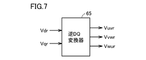
- FIG. 2 is a circuit block diagram illustrating a configuration of a signal generation circuit included in the control device illustrated in FIG. 1. It is a block diagram which shows the structure of the reactive power deviation calculating part contained in the control apparatus shown in FIG. It is a block diagram which shows the structure of the direct-current voltage control part and the reactive power control part which are contained in the control apparatus shown in FIG. It is a block diagram which shows the structure of the electric current control part contained in the control apparatus shown in FIG. It is a block diagram which shows the structure of the inverse DQ converter contained in the control apparatus shown in FIG.
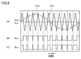
- FIG. 9 It is a circuit diagram which shows the structure of the gate signal generation circuit contained in the control apparatus shown in FIG. 9 is a time chart illustrating waveforms of the AC voltage command value Vuvr, the carrier signal Cuv, and the gate signals Auv and Buv illustrated in FIG. 8. 10 is a time chart illustrating the operation of the power conversion device shown in FIGS. 1 to 9; It is a time chart for demonstrating the comparative example of this Embodiment. It is a circuit diagram which shows the other comparative example of this Embodiment.
- FIG. 1 is a circuit block diagram showing a configuration of a power converter according to an embodiment of the present invention.
- this power converter is used as a reactive power compensator for compensating reactive power of the power system 1, and switches S1 to S6, transformers 2 and 3, current limiting resistors R1 to R3, AC line UL, VL, WL, current transformers C1 to C3, reactors L1 to L3, arms A1 to A3, and a control device 4 are provided.
- switches S1 to S3 are connected to the three-phase transmission lines 1u, 1v, 1w of the power system 1, respectively, and the other terminals are connected to the three primary windings of the transformer 2, respectively.
- Switches S1 to S3 are normally turned on, and are turned off, for example, during maintenance of the power converter.
- the transformer 2 includes three primary windings and three secondary windings, and transmits and receives three-phase AC power.
- One terminals of the current limiting resistors R1 to R3 are respectively connected to three secondary windings of the transformer 2, and the other terminals thereof are respectively connected to one terminals of the AC lines UL, VL, WL.
- Current limiting resistors R1 to R3 limit the current flowing from power system 1 to arms A1 to A3 when the power converter is activated.
- the switches S4 to S6 are connected in parallel to the current limiting resistors R1 to R3, respectively, and are turned on after the current flowing through the arms A1 to A3 is stabilized when the power converter is activated.
- the transformer 3 feeds back the AC voltages Vu, Vv, Vw having values corresponding to the AC voltages of the AC lines UL, VL, WL to the control device 4.
- Reactor L1 and arm A1 are connected in series between the other terminal of AC line UL and the other terminal of AC line VL.
- Reactor L2 and arm A2 are connected in series between the other terminal of AC line VL and the other terminal of AC line WL.
- Reactor L3 and arm A3 are connected in series between the other terminal of AC line WL and the other terminal of AC line UL. That is, the arms A1 to A3 are delta connected.
- Reactors L1 to L3 suppress the circulating current flowing through arms A1 to A3.
- Reactors L1 to L3 may be provided separately from arms A1 to A3, or may be inductance components of arms A1 to A3.
- the arms A1 to A3 are controlled by the control device 4 and generate three-phase AC power.
- Current transformers C1 to C3 feed back AC currents Iuv, Ivw, and Iwu having values corresponding to the AC currents flowing through arms A1 to A3 to control device 4, respectively.
- Each of the arms A1 to A3 includes a plurality (for example, 20) of unit converters 5 connected in cascade.
- Each of the plurality of unit converters 5 generates AC power in accordance with a control signal from the control device 4 or the like.
- FIG. 2 is a circuit block diagram showing the configuration of the unit converter 5.
- the unit converter 5 includes AC terminals 5 a and 5 b, a switch S ⁇ b> 7, an inverter 10, DC lines PL and NL, a capacitor 15, a voltage detector 16 (first detector), and a control unit 17.
- the AC terminals 5a of the first stage unit converters 5 of the arms A1 to A3 are connected to the other terminals of the AC lines UL, VL, and WL through the reactors L1 to L3, respectively.
- the AC terminal 5b of the final stage unit converter 5 of the arms A1 to A3 is connected to the other terminal of the AC lines VL, WL, and UL, respectively.
- the AC terminal 5a of each other unit converter 5 is connected to the AC terminal 5b of the previous unit converter 5, and the AC terminal 5b is connected to the AC terminal 5a of the next unit converter 5.
- the switch S7 is connected between the AC terminals 5a and 5b and is controlled by the control device 4, for example.
- the switch S7 is turned off when the corresponding unit converter 5 is normal, and is turned on when the corresponding unit converter 5 fails.
- the switch S7 is turned on, the AC terminals 5a and 5b are short-circuited, and the corresponding unit converter 5 is bypassed.
- the inverter 10 includes IGBTs (Insulated Gate Bipolar Transistors) 11 to 14 and diodes D1 to D4.
- the collectors of IGBTs 11 and 12 are both connected to positive DC line PL, and their emitters are connected to AC terminals 5a and 5b, respectively.
- the collectors of the IGBTs 13 and 14 are connected to the AC terminals 5a and 5b, respectively, and their emitters are both connected to the negative DC line NL.
- Each gate of IGBTs 11 to 14 receives a gate signal from control unit 17.
- Diodes D1-D4 are connected in antiparallel to IGBTs 11-14, respectively.
- the inverter 10 is subjected to DC voltage control and reactive power control by the control device 4 and the control unit 17, and transfers power between the power system 1 and the capacitor 15.
- Capacitor 15 is connected between DC lines PL and NL and stores DC power.
- the voltage detector 16 outputs a DC voltage VDC having a value corresponding to the DC voltage between the terminals of the capacitor 15 to the control unit 17.
- the control unit 17 is connected to the DC lines PL and NL, and is driven by the DC power stored in the capacitor 15.
- the control unit 17 operates the inverter 10 based on the gate signals Auv, Buv, Avw, Bvw, Awu, and Bwu from the control device 4, and sends a signal indicating the DC voltage VDC from the voltage detector 16 to the control device 4. Send.
- the control device 4 includes a reactive power command value Qr, AC voltages Vu, Vv, Vw from the transformer 3, AC currents Iuv, Ivw, Iwu from the current transformers C1 to C3, and unit converters. 5, each of the three arms A1 to A3 (that is, each of the 60 unit converters 5) is controlled.
- Reactive power command value Qr is given from the central command room of power system 1, for example.
- the power converter supplies reactive power having a value corresponding to the reactive power command value Qr to the power system 1.
- FIG. 3 is a circuit block diagram showing the configuration of the signal generation circuit 20 included in the control device 4.
- the signal generation circuit 20 includes a monitor voltage generation unit 21 and comparators 22-24.
- the monitor voltage generation unit 21 generates the monitor voltage VM based on the DC voltage VDC from the 60 unit converters 5. For example, the monitor voltage generator 21 selects the highest DC voltage VDC among the 60 DC voltages VDC, and outputs the selected DC voltage VDC as the monitor voltage VM.
- the comparator 22 compares the monitor voltage VM with the level of the protection level VH, and generates a protection signal P based on the comparison result.
- the protection signal P is set to the “H” level of the inactivation level.
- monitor voltage VM is higher than protection level VH (VM> VH)
- protection signal P is set to the “L” level of the activation level.
- the protection level VH is lower than the allowable level and higher than the rated value and command value of the DC voltage VDC.
- the comparator 23 compares the monitor voltage VM with the level of the return level V1 ( ⁇ VH), and generates the return signal B1 based on the comparison result.
- the return signal B1 is set to the inactivation level “H” level.
- the return signal B1 is set to the “L” level of the activation level.
- the return level V1 is a voltage lower than the protection level VH and higher than the rated value and the command value of the DC voltage VDC. After the electric power system 1 returns to normal from the accident, it is necessary to quickly restart the operation of the power converter. However, if the reactive power control of the inverter 10 is resumed immediately when the DC voltage VDC of the capacitor 15 becomes lower than the protection level VH, the reactive power is supplied from the power converter to the power system 1 and the voltage of the power system 1 increases. Then, the DC voltage VDC of the capacitor 15 rises again and exceeds the protection level VH. As a result, the operation and stop of the inverter 10 are repeated, and the power conversion device does not operate normally.
- the comparator 24 compares the monitor voltage VM with the level of the return level V2 ( ⁇ V1), and generates the return signal B2 based on the comparison result.
- monitor voltage VM is higher than return level V2 (VM> V2)
- return signal B2 is set to the inactivation level “H” level.
- the monitor voltage VM is equal to or lower than the return level V2 (VM ⁇ V2)
- the return signal B2 is set to the “L” level of the activation level.
- the return level V2 is a voltage lower than the return level V1 and higher than the rated value and the command value of the DC voltage VDC. Even if the voltage of the electric power system 1 rises and the DC voltage VDC of the capacitor 15 rises again because the reactive power control of the inverter 10 is resumed, the return level V2 does not cause the DC voltage VDC to exceed the protection level VH. It is set to such a value.
- FIG. 4 is a block diagram illustrating a configuration of the reactive power deviation calculation unit 30 included in the control device 4.
- the reactive power deviation calculation unit 30 includes a calculator 31, DQ converters 32 and 33, a reactive power calculator 34, and a subtractor 35.
- the computing unit 31 obtains AC currents Iu, Iv, Iw at a level corresponding to the AC current flowing in the AC lines UL, VL, WL based on the AC currents Iuv, Ivw, Iwu from the current transformers C1 to C3.
- the DQ converter 32 converts the three-phase alternating currents Iu, Iv, and Iw into a d-axis current Id and a q-axis current Iq.
- the DQ converter 33 converts the three-phase AC voltages Vu, Vv, Vw from the transformer 3 into a d-axis voltage Vd and a q-axis voltage Vq.
- the reactive power calculator 34 determines the reactive power Q based on the d-axis current Id, the q-axis current Iq, the d-axis voltage Vd, and the q-axis voltage Vq.
- the control device 4 further generates a DC voltage command value VDCr corresponding to the 60 unit converters 5.
- the DC voltage command value VDCr is given to 60 unit converters 5.
- DC voltage command value VDCr is normally set to a rated DC voltage.
- FIGS. 5A and 5B are block diagrams showing configurations of the DC voltage control unit 40 and the reactive power control unit 45.
- the DC voltage control unit 40 includes a flip-flop 41, a subtractor 42, a switching circuit 43, and a PI (Proportional Integral) control unit 44.
- DC voltage control unit 40 constitutes a first control unit that performs DC voltage control of inverter 10 such that DC voltage VDC of capacitor 15 becomes DC voltage command value VDCr.
- the flip-flop 41 is reset when both the protection signal P and the return signal B1 are at “H” level, and sets the output signal ⁇ 41 to “L” level (0).
- the flip-flop 41 is set when the protection signal P falls from the “H” level to the “L” level, and raises the output signal ⁇ 41 from the “L” level (0) to the “H” level (1).
- Signal ⁇ 41 is applied to each of switching circuit 43 and PI control unit 44.
- the switching circuit 43 gives the deviation ⁇ VDC from the subtractor 42 to the PI control unit 44 when the signal ⁇ 41 is at the “L” level (0), and “0” when the signal ⁇ 41 is at the “H” level (1). Is given to the PI control unit 44.
- the PI control unit 44 adds a value proportional to the output value ( ⁇ VDC or 0) of the switching circuit 43 and a value obtained by integrating the output value to generate a d-axis current command value Idr.
- signal ⁇ 41 is at “L” level (0)
- PI control unit 44 adds a value proportional to deviation ⁇ VDC from switching circuit 43 and a value obtained by integrating deviation ⁇ VDC to obtain d-axis current command value Idr. And the DC voltage of the inverter 10 is controlled.
- the reactive power control unit 45 includes a flip-flop 46, a switching circuit 47, and a PI control unit 48, as shown in FIG.
- the reactive power control unit 45 and the reactive power deviation calculation unit 30 of FIG. 4 perform reactive power control of the inverter 10 so that the reactive power Q exchanged between the capacitor 15 and the power system 1 becomes the reactive power command value Qr.
- the 2nd control part to perform is comprised.
- the flip-flop 46 is reset when the protection signal P and the return signal B2 are both at the “H” level, and sets the output signal ⁇ 46 to the “L” level (0).
- the flip-flop 46 is set when the protection signal P falls from the “H” level to the “L” level, and raises the output signal ⁇ 46 from the “L” level (0) to the “H” level (1).
- Signal ⁇ 46 is applied to each of switching circuit 47 and PI control unit 48.
- Switching circuit 47 provides reactive power deviation ⁇ Q from control device 4 to PI controller 48 when signal ⁇ 46 is at “L” level (0), and when signal ⁇ 46 is at “H” level (1). “0” is given to the PI control unit 48.
- the PI controller 48 adds a value proportional to the output value ( ⁇ Q or 0) of the switching circuit 47 and a value obtained by integrating the output value to generate a q-axis current command value Iqr.
- the PI control unit 48 adds the value proportional to the deviation ⁇ Q from the switching circuit 47 and the value obtained by integrating the deviation ⁇ Q to obtain the q-axis current command value Iqr. And the reactive power control of the inverter 10 is performed.
- FIGS. 6A and 6B are block diagrams showing the configuration of the current control units 50 and 60.
- the current control unit 50 includes a subtractor 51, a PI control unit 52, and an adder 53, as shown in FIG.
- the PI control unit 52 is controlled by the output signal ⁇ 41 of the flip-flop 41 (FIG. 5A).
- the PI control unit 52 adds the value proportional to the deviation ⁇ Id and the value obtained by integrating the deviation ⁇ Id to generate the d-axis voltage Vd1.
- the integral value in PI control unit 52 is reset to 0, and d-axis voltage Vd1 is fixed to 0.
- the adder 53 adds the d-axis voltage Vd from the DQ converter 33 to the d-axis voltage Vd1 from the PI control unit 52 to generate a d-axis voltage command value Vdr.
- the current control unit 60 includes a subtractor 61, a PI control unit 62, and an adder 63, as shown in FIG.
- the PI control unit 62 is controlled by the output signal ⁇ 41 of the flip-flop 41.
- the PI control unit 62 adds the value proportional to the deviation ⁇ Iq and the value obtained by integrating the deviation ⁇ Iq to generate the q-axis voltage Vq1.
- the signal ⁇ 41 is at “H” level (1), the integral value in the PI control unit 62 is reset to 0, and the q-axis voltage Vq1 is fixed to 0.
- Adder 63 adds q-axis voltage Vq from DQ converter 33 to q-axis voltage Vq1 from PI control unit 62 to generate q-axis voltage command value Vqr.
- FIG. 7 is a block diagram showing the configuration of the inverse DQ converter 65.
- the inverse DQ converter 65 performs inverse DQ conversion on the d-axis voltage command value Vdr and the q-axis voltage command value Vqr from the current control units 50 and 60 to obtain three-phase AC voltage command values Vuvr, Vvwr, and Vwur. Convert.
- Each of the three-phase AC voltage command values Vuvr, Vvwr, and Vwur is a sine wave, and the phases of the three-phase AC voltage command values Vuvr, Vvwr, and Vwur are shifted by 120 degrees.
- FIG. 8A, 8B, and 8C are circuit diagrams showing the configuration of the gate signal generation circuits 70, 80, and 90.
- the gate signal generation circuit 70 includes a comparator 72, a buffer 73, inverters 74 and 75, and AND gates 76 and 77.
- the comparator 72 compares the level of the AC voltage command value Vuvr and the level of the carrier signal Cuv, and outputs a signal ⁇ 72 of a level corresponding to the comparison result.
- the carrier signal Cuv is a triangular wave signal having a frequency higher than the AC voltage command value Vuvr and synchronized with the AC voltage command value Vuvr.
- Buffer 73 provides signal ⁇ 72 to one input node of AND gate 76.
- Inverter 74 inverts signal ⁇ 72 and applies the inverted signal to one input node of AND gate 77.
- Inverter 75 inverts output signal ⁇ 41 of flip-flop 41 (FIG. 5A) and applies the inverted signal to the other input node of AND gates 76 and 77.
- the output signals of the AND gates 76 and 77 are gate signals Auv and Buv, respectively.
- the gate signal Auv is applied to the gates of the IGBTs 11 and 14 included in the corresponding inverter 10, and the gate signal Buv is applied to the gates of the IGBTs 12 and 13 included in the corresponding inverter 10.
- the corresponding inverter 10 is operated by the gate signals Auv and Buv.
- the gate signals Auv and Buv are fixed at “L” level, and the operation of the corresponding inverter 10 is stopped.
- the gate signal generation circuit 80 includes a comparator 82, a buffer 83, inverters 84 and 85, and AND gates 86 and 87.
- the comparator 82 compares the level of the AC voltage command value Vvwr with the level of the carrier signal Cvw, and outputs a signal ⁇ 82 having a level corresponding to the comparison result.
- the carrier signal Cvw is a triangular wave signal having a frequency higher than the AC voltage command value Vvwr and synchronized with the AC voltage command value Vvwr.
- Buffer 83 provides signal ⁇ 82 to one input node of AND gate 86.
- Inverter 84 inverts signal ⁇ 82 and applies the inverted signal to one input node of AND gate 87.
- Inverter 85 inverts output signal ⁇ 41 of flip-flop 41 (FIG. 5A) and applies the inverted signal to the other input nodes of AND gates 86 and 87. Output signals of the AND gates 86 and 87 become gate signals Avw and Bvw, respectively.
- the gate signal Avw is applied to the gates of the IGBTs 11 and 14 included in the corresponding inverter 10, and the gate signal Bvw is applied to the gates of the IGBTs 12 and 13 included in the corresponding inverter 10.
- the corresponding inverter 10 is operated by the gate signals Avw and Bvw.
- signal ⁇ 41 is at “H” level, gate signals Avw and Bvw are fixed at “L” level, and operation of corresponding inverter 10 is stopped.
- the gate signal generation circuit 90 includes a comparator 92, a buffer 93, inverters 94 and 95, and AND gates 96 and 97.
- the comparator 92 compares the level of the AC voltage command value Vwur with the level of the carrier signal Cwu and outputs a signal ⁇ 92 having a level corresponding to the comparison result.
- the carrier signal Cwu is a triangular wave signal having a frequency higher than the AC voltage command value Vwur and synchronized with the AC voltage command value Vwur.
- Buffer 93 provides signal ⁇ 92 to one input node of AND gate 96.
- Inverter 94 inverts signal ⁇ 92 and applies the inverted signal to one input node of AND gate 97.
- Inverter 95 inverts output signal ⁇ 41 of flip-flop 41 (FIG. 5A) and applies the inverted signal to the other input nodes of AND gates 96 and 97.
- the output signals of the AND gates 96 and 97 become gate signals Awu and Bwu, respectively.
- the gate signal Awu is applied to the gates of the IGBTs 11 and 14 included in the corresponding inverter 10, and the gate signal Bwu is applied to the gates of the IGBTs 12 and 13 included in the corresponding inverter 10.
- the corresponding inverter 10 is operated by the gate signals Awu and Bwu.
- signal ⁇ 41 is at “H” level, gate signals Awu and Bwu are fixed at “L” level, and operation of corresponding inverter 10 is stopped.
- FIGS. 9A, 9B and 9C are time charts showing waveforms of the AC voltage command value Vuvr, the carrier signal Cuv, and the gate signals Auv and Buv shown in FIG. 8A.
- the AC voltage command value Vuvr is a sine wave signal
- the carrier signal Cuv is a triangular wave signal.
- the cycle of the carrier signal Cuv is shorter than the cycle of the AC voltage command value Vuvr, and the amplitude of the carrier signal Cuv is larger than the amplitude of the AC voltage command value Vuvr.
- the gate signal Auv becomes “L” level, and the level of the carrier signal Cuv becomes AC voltage command.
- the gate signal Auv becomes “H” level.
- the gate signal Auv is a positive pulse signal train.
- the pulse width of the gate signal Auv is large during the period in which the AC voltage command value Vuvr is positive, and the pulse width of the gate signal Auv is small during the period in which the AC voltage command value Vuvr is negative.
- the gate signal Buv is an inverted signal of the gate signal Auv.
- the IGBTs 11 and 14 included in the corresponding inverter 10 are turned on and the IGBTs 12 and 13 are turned off.
- the positive terminal (positive DC line PL) of the capacitor 15 is connected to the AC terminal 5a via the IGBT 11
- the AC terminal 5b is connected to the negative terminal (negative) of the capacitor 15 via the IGBT 14.
- Side voltage line NL Side voltage line NL
- the terminal voltage of the capacitor 15 is output between the AC terminals 5a and 5b. That is, a positive DC voltage is output between the AC terminals 5a and 5b.
- the IGBTs 12 and 13 included in the corresponding inverter 10 are turned on and the IGBTs 11 and 14 are turned off.
- the positive terminal (positive DC line PL) of the capacitor 15 is connected to the AC terminal 5b via the IGBT 12
- the AC terminal 5a is connected to the negative terminal (negative DC line) of the capacitor 15 via the IGBT 13. NL)
- the inter-terminal voltage of the capacitor 15 is output between the AC terminals 5b and 5a. That is, a negative DC voltage is output between the AC terminals 5a and 5b.
- the waveforms of the AC voltage command value Vvwr, the carrier signal Cvw, and the gate signals Avw and Bvw shown in FIG. 8B, and the AC voltage command value Vur, the carrier signal Cwu, and the gate signal Awu shown in FIG. , Bwu waveforms are the same as those of AC voltage command value Vuvr, carrier signal Cuv, and gate signals Auv, Buv shown in FIGS. 9A to 9C, and description thereof will not be repeated.
- FIGS. 10A, 10B, and 10C are time charts showing the operation of the power conversion apparatus shown in FIGS.
- FIGS. 10A and 10B show the signals ⁇ 41 and ⁇ 46 of FIGS. 5A and 5B, respectively
- FIG. 10C shows the DC voltage VDC selected as the monitor voltage VM. .
- the power system 1 switches S1 to S3, transformer 2, switches S4 to S6, AC lines UL, VL, WL in FIG.
- the effective current flows to the capacitor 15 of each unit converter 5 through the reactors L1 to L3, and the DC voltage VDC of the capacitor 15 rises.
- d-axis current command value Idr for performing DC voltage control of inverter 10 is set to 0, and gate signal generating circuits 70, 80, 90 are inactivated. And the gate signals Auv, Buv, Avw, Bvw, Awu, Bwu are all fixed at the “L” level.
- q-axis current command value Iqr for performing reactive power control of inverter 10 is set to zero. That is, the DC voltage control and reactive power control of the inverter 10 are stopped, and the switching of the IGBTs 11 to 14 is stopped.
- the return level V2 and the protection level VH are set so that the DC voltage VDC does not exceed the protection level VH. Therefore, even if DC voltage VDC exceeds return level V2, DC voltage control and reactive power control are continued, DC voltage VDC gradually decreases, and DC voltage VDC again coincides with DC voltage command value VDCr at time t5.
- a dotted line in FIG. 10C indicates a change in the DC voltage VDC of the capacitor 15 in the first comparative example.
- the DC voltage control and reactive power control of the inverter 10 are stopped, and when the DC voltage VDC drops below the return level V2, the DC voltage control and invalidity are performed. Power control is resumed at the same time.
- the DC voltage control of the inverter 10 since the DC voltage control of the inverter 10 is resumed when the DC voltage VDC drops below the return level V1, the DC voltage VDC is rapidly reduced from the return level V1 to the return level V2. be able to. Therefore, in the present embodiment, even when an accident occurs in the power system 1, the operation of the inverter 10 can be restarted quickly, and the reactive power compensation can be restarted quickly.
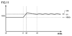
- FIG. 11 is a time chart showing the DC voltage VDC of the capacitor 15 in Comparative Example 2 of the present embodiment, which is compared with FIG. 10C.
- Comparative Example 2 when the DC voltage VDC exceeds the protection level VH (time t2), the DC voltage control and reactive power control of the inverter 10 are stopped, and when the DC voltage VDC drops below the return level V1 (time t3). ) Both DC voltage control and reactive power control are resumed.
- the reactive power control is restarted after the DC voltage VDC is lowered to the restoration level V2 that is sufficiently lower than the protection level VH by the DC voltage control. Does not vibrate between the protection level VH and the return level V1.
- FIG. 12 is a circuit diagram illustrating a main part of a power conversion device that is a third comparative example of the present embodiment.
- a resistance element 101 and a switch 102 are connected in series between the DC lines PL and NL of each unit converter.
- the switch 102 is normally turned off.
- Comparative Example 3 even when an accident occurs in the power system 1, the operation of the inverter 10 can be restarted quickly.
- the comparative example 3 it is necessary to provide the resistance element 101 and the switch 102 corresponding to each of the large number of capacitors 15, and there is a problem that the apparatus becomes large.
- the apparatus size since it is not necessary to provide the resistance element 101 and the switch 102, the apparatus size may be smaller than that of the comparative example 3.
- the apparatus can be reduced in size as compared with the case where the series connection body of the resistor element 101 and the switch 102 is connected in parallel to the capacitor 15.
- each of the arms A1 to A3 includes a plurality of unit converters 5
- each of the arms A1 to A3 includes only one unit converter 5. It can be applied to the case of inclusion.
- the return level V1 is set to a level lower than the protection level VH (V1 ⁇ VH).
- V1 VH
- 1 Power system 1u, 1v, 1w transmission line, S1 to S7,102 switch, 2,3 transformer, R1 to R3 current limiting resistor, UL, VL, WL AC line, C1 to C3 current transformer, L1 to L3 reactor, A1 to A3 arm, 4 control device, 5 unit converter, 5a, 5b AC terminal, 10, 74, 75, 84, 85, 94, 95 inverter, 11-14 IGBT, PL, NL DC line, 15 Capacitor, 16 voltage detector, 17 controller, 20 signal generator, 21 monitor voltage generator, 22-24, 72, 82, 92 comparator, 30 reactive power deviation calculator, 31 calculator, 32, 33 DQ conversion , 34 reactive power calculator, 35, 42, 51, 61 subtractor, 40 DC voltage controller, 41, 46 flip-flop, 43, 7 switching circuit, 44, 48, 52, 62 PI control unit, 45 reactive power control unit, 50, 60 current control unit, 53, 63 adder, 65 inverse DQ converter, 70, 80, 90 gate signal generation
Landscapes
- Engineering & Computer Science (AREA)
- Power Engineering (AREA)
- Inverter Devices (AREA)
- Control Of Electrical Variables (AREA)
Abstract
Dans un dispositif de conversion de puissance selon l'invention, le fonctionnement d'un onduleur (10) est arrêté lorsqu'un défaut se produit dans un système d'alimentation (1) et que la tension continue (Vcc) d'un condensateur (15) compris dans un convertisseur unitaire (5) dépasse un niveau de protection (VH), la commande de tension continue de l'onduleur (10) est redémarrée et la tension continue (Vcc) est rapidement abaissée lorsque la tension continue (Vcc) descend à un niveau de retour (V1) ou en dessous de celui-ci, et la commande de puissance réactive de l'onduleur (10) est redémarrée lorsque la tension continue (Vcc) descend à un niveau de retour (V2) ou en dessous de celui-ci. Par conséquent, le fonctionnement de l'onduleur (10) peut être redémarré rapidement même lorsqu'un défaut se produit dans le système d'alimentation (1).
Priority Applications (4)
| Application Number | Priority Date | Filing Date | Title |
|---|---|---|---|
| US16/494,923 US10826383B2 (en) | 2017-03-22 | 2017-03-22 | Power conversion device |
| JP2019506789A JP6748290B2 (ja) | 2017-03-22 | 2017-03-22 | 電力変換装置 |
| PCT/JP2017/011405 WO2018173144A1 (fr) | 2017-03-22 | 2017-03-22 | Dispositif de conversion de puissance |
| EP17901397.4A EP3605822B1 (fr) | 2017-03-22 | 2017-03-22 | Dispositif de conversion de puissance |
Applications Claiming Priority (1)
| Application Number | Priority Date | Filing Date | Title |
|---|---|---|---|
| PCT/JP2017/011405 WO2018173144A1 (fr) | 2017-03-22 | 2017-03-22 | Dispositif de conversion de puissance |
Publications (1)
| Publication Number | Publication Date |
|---|---|
| WO2018173144A1 true WO2018173144A1 (fr) | 2018-09-27 |
Family
ID=63585083
Family Applications (1)
| Application Number | Title | Priority Date | Filing Date |
|---|---|---|---|
| PCT/JP2017/011405 WO2018173144A1 (fr) | 2017-03-22 | 2017-03-22 | Dispositif de conversion de puissance |
Country Status (4)
| Country | Link |
|---|---|
| US (1) | US10826383B2 (fr) |
| EP (1) | EP3605822B1 (fr) |
| JP (1) | JP6748290B2 (fr) |
| WO (1) | WO2018173144A1 (fr) |
Cited By (1)
| Publication number | Priority date | Publication date | Assignee | Title |
|---|---|---|---|---|
| WO2021166164A1 (fr) * | 2020-02-20 | 2021-08-26 | 三菱電機株式会社 | Dispositif de conversion de puissance et système d'alimentation d'avion |
Families Citing this family (2)
| Publication number | Priority date | Publication date | Assignee | Title |
|---|---|---|---|---|
| US11201461B2 (en) * | 2017-06-08 | 2021-12-14 | Mitsubishi Electric Corporation | Power control system and control device for restoring AC system from power failure |
| CN116470820A (zh) * | 2022-01-12 | 2023-07-21 | 台达电子工业股份有限公司 | 三相功率转换器的输出电流的箝位控制方法 |
Citations (4)
| Publication number | Priority date | Publication date | Assignee | Title |
|---|---|---|---|---|
| JP2002281670A (ja) * | 2001-03-19 | 2002-09-27 | Mitsubishi Electric Corp | 電力変換装置 |
| WO2012099176A1 (fr) | 2011-01-18 | 2012-07-26 | 国立大学法人東京工業大学 | Convertisseur de secteur et son procédé de commande |
| JP2016100926A (ja) * | 2014-11-19 | 2016-05-30 | 三菱電機株式会社 | 電力変換装置 |
| WO2016167117A1 (fr) * | 2015-04-13 | 2016-10-20 | 三菱電機株式会社 | Dispositif de conversion d'énergie électrique et système d'énergie électrique |
Family Cites Families (4)
| Publication number | Priority date | Publication date | Assignee | Title |
|---|---|---|---|---|
| US5642275A (en) * | 1995-09-14 | 1997-06-24 | Lockheed Martin Energy System, Inc. | Multilevel cascade voltage source inverter with seperate DC sources |
| JP6099951B2 (ja) * | 2012-11-29 | 2017-03-22 | 株式会社東芝 | 電力変換装置 |
| CN104753043B (zh) * | 2015-03-27 | 2017-05-17 | 山东大学 | 一种具有直流故障穿越能力的多电平换流器及工作方法 |
| FR3038796B1 (fr) * | 2015-07-09 | 2017-08-11 | Moteurs Leroy-Somer | Systeme de generation d'energie a traitement ameliore des impacts a charge, des delestages et des harmoniques |
-
2017
- 2017-03-22 JP JP2019506789A patent/JP6748290B2/ja active Active
- 2017-03-22 WO PCT/JP2017/011405 patent/WO2018173144A1/fr unknown
- 2017-03-22 EP EP17901397.4A patent/EP3605822B1/fr active Active
- 2017-03-22 US US16/494,923 patent/US10826383B2/en active Active
Patent Citations (4)
| Publication number | Priority date | Publication date | Assignee | Title |
|---|---|---|---|---|
| JP2002281670A (ja) * | 2001-03-19 | 2002-09-27 | Mitsubishi Electric Corp | 電力変換装置 |
| WO2012099176A1 (fr) | 2011-01-18 | 2012-07-26 | 国立大学法人東京工業大学 | Convertisseur de secteur et son procédé de commande |
| JP2016100926A (ja) * | 2014-11-19 | 2016-05-30 | 三菱電機株式会社 | 電力変換装置 |
| WO2016167117A1 (fr) * | 2015-04-13 | 2016-10-20 | 三菱電機株式会社 | Dispositif de conversion d'énergie électrique et système d'énergie électrique |
Non-Patent Citations (1)
| Title |
|---|
| See also references of EP3605822A4 |
Cited By (2)
| Publication number | Priority date | Publication date | Assignee | Title |
|---|---|---|---|---|
| WO2021166164A1 (fr) * | 2020-02-20 | 2021-08-26 | 三菱電機株式会社 | Dispositif de conversion de puissance et système d'alimentation d'avion |
| JPWO2021166164A1 (fr) * | 2020-02-20 | 2021-08-26 |
Also Published As
| Publication number | Publication date |
|---|---|
| JPWO2018173144A1 (ja) | 2020-01-16 |
| EP3605822B1 (fr) | 2022-03-02 |
| US10826383B2 (en) | 2020-11-03 |
| US20200287455A1 (en) | 2020-09-10 |
| EP3605822A4 (fr) | 2020-12-16 |
| EP3605822A1 (fr) | 2020-02-05 |
| JP6748290B2 (ja) | 2020-08-26 |
Similar Documents
| Publication | Publication Date | Title |
|---|---|---|
| Ceballos et al. | Three-level converter topologies with switch breakdown fault-tolerance capability | |
| JP5894777B2 (ja) | 電力変換装置 | |
| JP5049964B2 (ja) | 電力変換装置 | |
| Sepahvand et al. | Start-up procedure and switching loss reduction for a single-phase flying capacitor active rectifier | |
| WO2007129456A1 (fr) | Convertisseur de puissance | |
| WO2018179145A1 (fr) | Dispositif de conversion de puissance et son procédé d'essai | |
| JP6666058B2 (ja) | 系統連系インバータ装置及びその運転方法 | |
| JP6748290B2 (ja) | 電力変換装置 | |
| JP2018129963A (ja) | 電力変換器の制御装置 | |
| JP2011193589A (ja) | 電力変換装置 | |
| JP2016174490A (ja) | 電力変換装置 | |
| JP5459304B2 (ja) | 電流形電力変換装置 | |
| JP5739734B2 (ja) | 電力変換装置 | |
| JP6676830B1 (ja) | 電力変換装置 | |
| JP5490263B2 (ja) | 電力変換装置 | |
| JP6690880B2 (ja) | 電力変換装置 | |
| JP6512710B2 (ja) | 電力変換装置 | |
| JP2013106368A (ja) | 電力変換装置 | |
| JP5894031B2 (ja) | 電力変換装置 | |
| JP5752580B2 (ja) | 電力変換装置 | |
| WO2023214462A1 (fr) | Dispositif de conversion de puissance | |
| JP6614704B2 (ja) | 電力変換装置 | |
| JP2017175862A (ja) | 電力変換装置 | |
| WO2019102610A1 (fr) | Dispositif de conversion de puissance |
Legal Events
| Date | Code | Title | Description |
|---|---|---|---|
| 121 | Ep: the epo has been informed by wipo that ep was designated in this application |
Ref document number: 17901397 Country of ref document: EP Kind code of ref document: A1 |
|
| ENP | Entry into the national phase |
Ref document number: 2019506789 Country of ref document: JP Kind code of ref document: A |
|
| NENP | Non-entry into the national phase |
Ref country code: DE |
|
| ENP | Entry into the national phase |
Ref document number: 2017901397 Country of ref document: EP Effective date: 20191022 |