WO2018131285A1 - フレキシブルプリント基板の製造方法及びフレキシブルプリント基板 - Google Patents
フレキシブルプリント基板の製造方法及びフレキシブルプリント基板 Download PDFInfo
- Publication number
- WO2018131285A1 WO2018131285A1 PCT/JP2017/041053 JP2017041053W WO2018131285A1 WO 2018131285 A1 WO2018131285 A1 WO 2018131285A1 JP 2017041053 W JP2017041053 W JP 2017041053W WO 2018131285 A1 WO2018131285 A1 WO 2018131285A1
- Authority
- WO
- WIPO (PCT)
- Prior art keywords
- layer
- insulating resin
- hole
- photosensitive insulating
- conductive
- Prior art date
- Legal status (The legal status is an assumption and is not a legal conclusion. Google has not performed a legal analysis and makes no representation as to the accuracy of the status listed.)
- Ceased
Links
Images







Classifications
-
- H—ELECTRICITY
- H05—ELECTRIC TECHNIQUES NOT OTHERWISE PROVIDED FOR
- H05K—PRINTED CIRCUITS; CASINGS OR CONSTRUCTIONAL DETAILS OF ELECTRIC APPARATUS; MANUFACTURE OF ASSEMBLAGES OF ELECTRICAL COMPONENTS
- H05K1/00—Printed circuits
- H05K1/02—Details
- H05K1/11—Printed elements for providing electric connections to or between printed circuits
-
- H—ELECTRICITY
- H05—ELECTRIC TECHNIQUES NOT OTHERWISE PROVIDED FOR
- H05K—PRINTED CIRCUITS; CASINGS OR CONSTRUCTIONAL DETAILS OF ELECTRIC APPARATUS; MANUFACTURE OF ASSEMBLAGES OF ELECTRICAL COMPONENTS
- H05K3/00—Apparatus or processes for manufacturing printed circuits
- H05K3/40—Forming printed elements for providing electric connections to or between printed circuits
-
- H—ELECTRICITY
- H05—ELECTRIC TECHNIQUES NOT OTHERWISE PROVIDED FOR
- H05K—PRINTED CIRCUITS; CASINGS OR CONSTRUCTIONAL DETAILS OF ELECTRIC APPARATUS; MANUFACTURE OF ASSEMBLAGES OF ELECTRICAL COMPONENTS
- H05K3/00—Apparatus or processes for manufacturing printed circuits
- H05K3/46—Manufacturing multilayer circuits
Definitions
- the present invention relates to a method for manufacturing a flexible printed circuit board and a flexible printed circuit board.
- via holes may be formed to connect wirings of different layers, and conductive members may be embedded in the via holes.
- the via hole was previously formed by a mechanical drill, but recently, it is often formed by a laser.
- the present invention has been made in view of the above points, and an object of the present invention is to provide a method for manufacturing a flexible printed board including a step of forming via holes in a short time without leaving smears.
- One aspect of a method for manufacturing a flexible printed circuit board that solves the above-described problems includes a step of providing a first photosensitive insulating resin layer on one surface of a first conductive layer, and a step of providing the first photosensitive insulating resin layer A step of forming a first hole reaching the first conductive layer by photolithography, and a surface of the first photosensitive insulating resin layer opposite to the surface in contact with the first conductive layer.
- Providing the first wiring layer, and in the step of providing the first wiring layer the first wiring layer is formed by the first conductive member provided in the first hole.
- the conductive layer is electrically connected.
- a wiring pattern may be formed on the first conductive layer.
- the opening area on the first wiring layer side of the first hole may be smaller than the opening area on the first conductive layer side.
- An insulating resin film is provided on the other surface of the first conductive layer, and a second conductive layer is formed on the surface of the insulating resin film opposite to the surface in contact with the first conductive layer. And providing a second photosensitive insulating resin layer on a surface of the second conductive layer opposite to the surface in contact with the insulating resin film, and the second photosensitive insulation.
- Providing a second wiring layer on the surface of the second wiring layer, and in the step of providing the second wiring layer, the second wiring layer is formed by a second conductive member provided in the second hole. May be electrically connected to the second conductive layer.
- a wiring pattern may be formed on the second conductive layer.
- a through-hole may be provided in the insulating resin film to make the first conductive layer and the second conductive layer conductive.
- the opening area on the second wiring layer side of the second hole may be smaller than the opening area on the second conductive layer side.
- Providing a layer with a third hole reaching the first wiring layer by photolithography, and a surface of the third photosensitive insulating resin layer opposite to the surface in contact with the first wiring layer A step of providing a third wiring layer on the surface, and in the step of providing the third wiring layer, the third wiring layer is formed by a third conductive member provided in the third hole.
- the first wiring layer may be electrically connected.
- the first hole and the second hole may be provided at the same time.
- mode of the flexible printed circuit board which solves the above-mentioned subject is the insulating resin film, the conductive layer provided on the said insulating resin film, and the photosensitive insulating resin layer provided on the said conductive layer,
- a wiring layer provided on the photosensitive insulating resin layer, and the photosensitive insulating resin layer includes a hole reaching the conductive layer, and the conductive layer and the wiring layer are provided in the hole. And a conductive member for electrically connecting the two.
- the photosensitive insulating resin layer is cured by light irradiation, and the opening area of the hole on the wiring layer side may be smaller than the opening area on the conductive layer side.
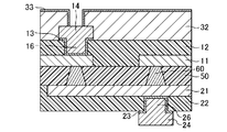
- FIG. 1 It is a schematic diagram which shows the cross section of 2 layer CCL. It is typical sectional drawing of FPC which has the 2 layer wiring pattern by which the interlayer connection was made
- Embodiment 1 The manufacturing method of the flexible printed circuit board concerning Embodiment 1 is demonstrated based on FIGS. 1-7.
- a flexible two-layer CCL in which metal layers 10 and 20 are provided on both surfaces of an insulating resin film 50 is prepared.
- the insulating resin film 50 is made of, for example, a polyimide film, and preferably has a thickness of about 5 ⁇ m to 50 ⁇ m so that it can be bent.
- the metal layers 10 and 20 are made of a metal thin film, and are preferably a copper thin film from the viewpoint of cost and conductivity, and the thickness is preferably 0.2 ⁇ m to 2 ⁇ m.
- the first conductive layer 11 and the second conductive layer 21 having a wiring pattern are formed on both surfaces of the two-layer CCL, and a through hole is provided in the insulating resin film 50 to fill the through hole with a conductive material.
- the conduction between the conductive layer 11 and the second conductive layer 21 is ensured (FIG. 2).
- the metal layer 20 is etched to form a hole, and a portion of the insulating resin film 50 exposed from the hole is etched to form a through hole.
- pattern etching is performed on the metal layers 10 and 20 to form a wiring pattern, and metal plating is further performed on the wiring pattern to increase the thickness of the conductive layer.
- a method of forming the conductive layer 11 and the second conductive layer 21 may be performed. This method is one example, and another method may be used.
- the first photosensitive insulating resin layer 12 is provided on the upper surface of the first conductive layer 11 (the surface opposite to the surface in contact with the insulating resin film 50).
- the second photosensitive insulating resin layer 22 is provided on the lower surface of the conductive layer 21 (the surface opposite to the surface in contact with the insulating resin film 50).
- the first and second photosensitive insulating resin layers 12 and 22 may be formed, for example, by laminating a photosensitive polyimide film or by applying a photosensitive varnish, and the thickness thereof is 5 ⁇ m to 50 ⁇ m. The degree is preferred.
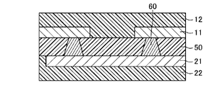
- the first hole 15 is provided in the first photosensitive insulating resin layer 12 and the second hole 25 is provided in the second photosensitive insulating resin layer 22 by photolithography. That is, the first hole 15 and the second hole 25 are formed by performing masking / exposure so that only the portions of the first hole 15 and the second hole 25 are not cured, and removing with a chemical solution.
- the first hole 15 that is a via hole reaches the first conductive layer 11, and the second hole 25 reaches the second conductive layer 21.
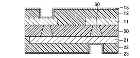
- the conductive thin films 13, 25 are formed by sputtering or the like on the entire exposed surfaces of the first and second photosensitive insulating resin layers 12, 22 in which the first and second holes 15, 25 are formed. 23 is formed. Then, a pattern mask is formed on both surfaces by photolithography, and the first hole 15 is embedded using the first conductive member 16 and the second hole 25 is embedded using the second conductive member 26 by plating.
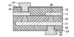
- first wiring layer 14 and the second wiring layer 24 are respectively formed on the first photosensitive insulating resin layer 12 (on the side opposite to the surface in contact with the first conductive layer 11), and the second It is provided under the photosensitive insulating resin layer 22 (on the side opposite to the surface in contact with the second conductive layer 21) (FIG. 6). Thereafter, by leaving only the conductive thin films 13 and 23 existing immediately below the first wiring layer 14 and immediately above the second wiring layer 24, the other conductive thin films 13 and 23 are removed by etching. A four-layer wiring pattern shown in FIG. 7 is laminated, and a flexible printed circuit board in which adjacent upper and lower wiring patterns are connected is completed.
- the first photosensitive insulating resin layer 12 is provided between the first conductive layer 11 and the first wiring layer 14 and between the second conductive layer 21 and the second wiring layer 24.
- the first hole 15 and the second hole 25 for via connection between the two can be formed by photolithography.
- the uncured photosensitive insulating resin dissolves in the chemical solution and is reliably removed, so that the inside of the hole and the first photosensitive insulating material are removed.
- Residue of the photosensitive insulating resin does not remain on the surfaces of the resin layer 12 and the second photosensitive insulating resin layer 22, and the via connection is reliably performed, and the first wiring layer 14 and the second wiring layer 24 are also reliable.
- the wiring pattern can be high. Furthermore, since no residue remains, the inspection after the formation of the hole can be easily performed, and depending on the formation conditions, the inspection can be omitted, the manufacturing time can be shortened, and the cost can be reduced. Moreover, since the hole making by lithography can process all the holes in the substrate at once, the manufacturing time can be similarly reduced and the cost can be reduced.
- the material types and thicknesses of the first and second photosensitive insulating resin layers 12 and 22, the first and second conductive layers 11 and 21, and the first and second wiring layers 14 and 24 are appropriately set. This makes it possible to manufacture a flexible printed board that is thin and easy to bend.
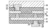
- the third photosensitive insulating resin layer 32 is provided.
- a third hole 35 is provided in the third photosensitive insulating resin layer 32 by photolithography.
- the third hole 35 that is a via hole reaches the first wiring layer 14.
- a conductive thin film 33 is formed by sputtering or the like on the entire exposed upper surface of the third photosensitive insulating resin layer 32 in which the third hole 35 is formed.
- a pattern mask is formed on the conductive thin film 33 by photolithography, and the third hole 35 is embedded by using the third conductive member 36 by plating, and the third wiring layer 34 is third photosensitive.
- 11 is provided on the insulating insulating resin layer 32 (on the side opposite to the surface in contact with the first wiring layer 14) (FIG. 11).
- another wiring layer may be formed on the surface of the second wiring layer 24 by the same method, and a wiring layer may be further overlapped on both surfaces in the same manner.
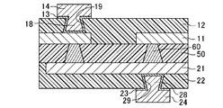
- the third embodiment differs from the first embodiment in the shapes of the first hole 15 and the second hole 25, and therefore the shapes of the first conductive member 16 and the second conductive member 26 are different. Since the other points are the same as those in the first embodiment, the points different from the first embodiment will be described below.
- the opening area on the first wiring layer 14 side of the first hole 19 is smaller than the opening area on the first conductive layer 11 side.
- the opening area on the second wiring layer 24 side is smaller than the opening area on the second conductive layer 21 side. That is, when the first hole 19 and the second hole 29 are formed, the holes 19 and 29 have a tapered shape whose diameter decreases toward the opening. Since the 1st hole 19 and the 2nd hole 29 have such a shape, the 1st conductive member 18 and the 2nd conductive member 28 which were embed
- the first wiring layer 14 and the second wiring layer 24 are firmly formed and have high reliability.
- the raw materials of the first photosensitive insulating resin layer 12 and the second photosensitive insulating resin layer 22 are irradiated with light.
- a method of controlling the amount of light irradiation in the photolithography process to be a small amount can be considered.
- the photosensitive insulating resin layer in the portion irradiated with light outside the edge becomes insufficiently cured as it approaches the bottom, and the bottom in the development for opening the hole It is because the part which is not masked will also melt
- the material prepared first is not limited to the two-layer CCL, and may be a three-layer CCL or a CCL having a metal layer only on one side.
- copper foil may be sufficient.
- a photosensitive insulating resin layer or a wiring layer may be laminated only on them, or a photosensitive insulating resin layer is also formed on the lower surface side.
- a wiring layer may be laminated, and in the case of a thin film, it may be supported by a support material such as PET, or a pre-laminated material may be used.
- each photosensitive insulating resin layer may be positive or negative.
- the same thing for example, the photosensitive coverlay film of the same product number
- the thing from which a kind, material, and thickness differ may be used, respectively.
- each conductive member It is not necessary to fill the first hole, the second hole, and the third hole with each conductive member.
- a conductive thin film may be used as each conductive member, and the conductive thin film may be electrically connected to the first wiring layer, the second wiring layer, and the third wiring layer.
- first hole and the second hole are formed separately.
- the conductive thin film formed in each hole is preferably formed to have a thickness of 2 ⁇ m or less by using, for example, nichrome sputtering or a combination of nichrome sputtering and copper sputtering.
- a conductive thin film forming method can be used.
- the plating layer provided on a conductive thin film is not specifically limited, For example, using copper is mentioned. In this case, the conductive member is copper by plating.
Landscapes
- Engineering & Computer Science (AREA)
- Microelectronics & Electronic Packaging (AREA)
- Manufacturing & Machinery (AREA)
- Printing Elements For Providing Electric Connections Between Printed Circuits (AREA)
- Production Of Multi-Layered Print Wiring Board (AREA)
Abstract
ビアホール形成をスミアを残さず短時間で行う工程を含むフレキシブルプリント 基板の製造方法を提供する。 具体的には、フレキシブルプリント基板の製造方法は、第1の導電層の一方の面に第1の感光性絶縁樹脂層を設ける工程と、前記第1の感光性絶縁樹脂層に、フォトリソグラフィによって前記第1の導電層に達する第1の穴を設ける工程と、前記第1の感光性絶縁樹脂層の、前記第1の導電層に接している面とは反対側の面に第1の配線層を設ける工程とを含み、前記第1の配線層を設ける工程では、前記第1の穴の中に設けられた第1の導電部材によって前記第1の配線層を前記第1の導電層に電気的に導通させている。
Description
本発明は、フレキシブルプリント基板の製造方法及びフレキシブルプリント基板に関するものである。
電子機器の小型化の要請は近年益々強まっており、電子機器内の部品や部品を搭載する基板を小さくする技術開発が進められている。基板を多層プリント基板とすることで電子機器を小型化することができるため、多層プリント基板の開発が進められている。
多層プリント基板では、層の異なる配線同士を接続させるためビアホールを形成し、ビアホール内に導電性の部材を埋設している場合がある。このような場合、以前はビアホールを機械式のドリルで形成していたが、最近はレーザにより形成することが多くなっている。
レーザによるビアホールの穴開けでは、スミアと呼ばれる残渣がビアホールの底やビアホール近傍の表面に残るという問題があった。スミアが残ったまま後工程を行うと、導通不良及び層間の密着不良の原因となってしまうので、湿式法によってスミアを除去する工程およびスミア残りがないことを確認する検査工程が穴開け工程の後に設けられるためコスト増となっている。さらに、ビア径が小さくなるとビアホールの底に残ったスミアを除去することが困難になり、スミアが除去されたか否かの検査も困難になり、且つ検査に時間がかかってしまう。この問題を緩和するために特許文献1,2に開示されている技術が提案されている。
しかしながら、特許文献1,2に開示された技術をもってしてもレーザ加工だけではスミアを完全に取り除くことはできず、レーザ加工を行った後に湿式法によってスミアを除去する工程が必要であり、ビア径が小さくなると生じる問題にも対応が不完全で、コストと加工時間が増大してしまうという問題があった。
本発明は、かかる点に鑑みてなされたものであり、その目的とするところは、ビアホール形成をスミアを残さず短時間で行う工程を含むフレキシブルプリント基板の製造方法を提供することにある。
上述の課題を解決するフレキシブルプリント基板の製造方法の一態様は、第1の導電層の一方の面に第1の感光性絶縁樹脂層を設ける工程と、前記第1の感光性絶縁樹脂層に、フォトリソグラフィによって前記第1の導電層に達する第1の穴を設ける工程と、前記第1の感光性絶縁樹脂層の、前記第1の導電層に接している面とは反対側の面に第1の配線層を設ける工程とを含み、前記第1の配線層を設ける工程では、前記第1の穴の中に設けられた第1の導電部材によって前記第1の配線層を前記第1の導電層に電気的に導通させている。第1の導電層には配線パターンが形成されていてもよい。
前記第1の穴は、前記第1の導電層側の開口面積よりも前記第1の配線層側の開口面積の方が小さくてもよい。
前記第1の導電層の他方の面には絶縁樹脂フィルムが設けられており、前記絶縁樹脂フィルムの、前記第1の導電層に接している面とは反対側の面に第2の導電層が設けられているとともに、前記第2の導電層の、前記絶縁樹脂フィルムに接した面とは反対側の面に第2の感光性絶縁樹脂層を設ける工程と、前記第2の感光性絶縁樹脂層に、フォトリソグラフィによって前記第2の導電層に達する第2の穴を設ける工程と、前記第2の感光性絶縁樹脂層の、前記第2の導電層に接している面とは反対側の面に第2の配線層を設ける工程とをさらに含み、前記第2の配線層を設ける工程では、前記第2の穴の中に設けられた第2の導電部材によって前記第2の配線層を前記第2の導電層に電気的に導通させていてもよい。第2の導電層には配線パターンが形成されていてもよい。また、絶縁樹脂フィルムに貫通孔を設けて第1の導電層と第2の導電層とを導通させてもよい。
前記第2の穴は、前記第2の導電層側の開口面積よりも前記第2の配線層側の開口面積の方が小さくてもよい。
前記第1の配線層の、前記第1の感光性絶縁樹脂層に接している面とは反対側の面に第3の感光性絶縁樹脂層を設ける工程と、前記第3の感光性絶縁樹脂層に、フォトリソグラフィによって前記第1の配線層に達する第3の穴を設ける工程と、前記第3の感光性絶縁樹脂層の、前記第1の配線層に接している面とは反対側の面に第3の配線層を設ける工程とをさらに含み、前記第3の配線層を設ける工程では、前記第3の穴の中に設けられた第3の導電部材によって前記第3の配線層を前記第1の配線層に電気的に導通させていてもよい。
前記第1の穴と前記第2の穴とは同時に設けられてもよい。
また、上述の課題を解決するフレキシブルプリント基板の一態様は、絶縁樹脂フィルムと、前記絶縁樹脂フィルムの上に設けられた導電層と、前記導電層の上に設けられた感光性絶縁樹脂層と、前記感光性絶縁樹脂層の上に設けられた配線層とを備え、前記感光性絶縁樹脂層は前記導電層に達する穴を備えており、前記穴の中には前記導電層と前記配線層とを電気的に導通させる導電部材が配されている。
前記感光性絶縁樹脂層は光照射によって硬化しており、前記穴は前記導電層側の開口面積よりも前記配線層側の開口面積の方が小さくてもよい。
感光性絶縁樹脂層を用い、フォトリソグラフィによって穴を開けるので、スミアが残らず、低コストで信頼性の高いビア接続を備えたフレキシブルプリント基板を作成することができる。
以下、本発明の実施形態を図面に基づいて詳細に説明する。以下の好ましい実施形態の説明は、本質的に例示に過ぎず、本発明、その適用物或いはその用途を制限することを意図するものではない。以下の図面においては、説明の簡潔化のため、実質的に同一の機能を有する構成要素を同一の参照符号で示す。また、以下の説明における上下関係は、図面における上下の関係を指している。
(実施形態1)
実施形態1に係るフレキシブルプリント基板の製造方法を図1から図7に基づいて説明する。
実施形態1に係るフレキシブルプリント基板の製造方法を図1から図7に基づいて説明する。
図1に示すように、まず絶縁樹脂フィルム50の両面に金属層10,20を設けたフレキシブル2層CCLを用意する。絶縁樹脂フィルム50は例えばポリイミドフィルムからなり、曲げられるように厚みは5μm~50μm程度であることが好ましい。金属層10,20は金属薄膜からなり、コストおよび導電性の高さから銅薄膜であることが好ましく、その厚みは0.2μm~2μmであることが好ましい。
この2層CCLの両面に、配線パターンを有する第1の導電層11及び第2の導電層21を形成すると共に、絶縁樹脂フィルム50に貫通孔を設けその貫通孔を導電物質によって埋めて第1の導電層11及び第2の導電層21の間の導通を確保する(図2)。このような層間接続されたFPCを作成するには、例えば、金属層20をエッチングして穴を形成し、その穴から露出した絶縁樹脂フィルム50の部分をエッチングにより貫通孔を形成し、その貫通孔にめっきにより銅を埋め込んだ後、金属層10,20に対してパターンエッチングを行って配線パターンを形成し、さらにその配線パターン上に金属めっきを行って導電層厚みを大きくして第1の導電層11及び第2の導電層21を形成する、という方法で行えばよい。なお、この方法は1つの例であり、別の方法で行っても構わない。
次に、図3に示すように、第1の導電層11の上面(絶縁樹脂フィルム50に接した面とは反対側の面)に第1の感光性絶縁樹脂層12を設けるとともに、第2の導電層21の下面(絶縁樹脂フィルム50に接した面とは反対側の面)に第2の感光性絶縁樹脂層22を設ける。第1及び第2の感光性絶縁樹脂層12,22は、例えば感光性ポリイミドフィルムを貼り合わせて形成したり、感光性のワニスを塗布して形成したりすればよく、その厚みは5μm~50μm程度が好ましい。
それから図4に示すように、フォトリソグラフィによって第1の感光性絶縁樹脂層12に第1の穴15を、第2の感光性絶縁樹脂層22に第2の穴25を設ける。即ち、第1の穴15,第2の穴25の部分のみが硬化しないようにマスク・露光を行って、薬液によって除去することにより、第1の穴15,第2の穴25を形成する。ビアホールである第1の穴15は第1の導電層11にまで達しており、第2の穴25は第2の導電層21にまで達している。
さらに図5に示すように第1及び第2の穴15,25を形成した第1及び第2の感光性絶縁樹脂層12,22の露出している面の全面にスパッタ等により導電薄膜13,23を形成する。そして、フォトリソグラフィにより両面にパターンマスクを形成し、めっきによって、第1の穴15を第1の導電部材16を用いて埋設し、第2の穴25を第2の導電部材26を用いて埋設すると共に、第1の配線層14及び第2の配線層24をそれぞれ第1の感光性絶縁樹脂層12の上(第1の導電層11に接している面とは反対側)、第2の感光性絶縁樹脂層22の下(第2の導電層21に接している面とは反対側)に設ける(図6)。その後、第1の配線層14の直下及び第2の配線層24の直上に存在している導電薄膜13,23のみを残して、それ以外の導電薄膜13,23をエッチングによって除去することにより、図7に示す4層の配線パターンが積層されて、隣接する上下の配線パターン同士が接続されたフレキシブルプリント基板が出来上がる。
本実施形態では、第1の導電層11と第1の配線層14との間、及び第2の導電層21と第2の配線層24との間にそれぞれ第1の感光性絶縁樹脂層12及び第2の感光性絶縁樹脂層22を介在させることにより、第1の導電層11と第1の配線層14との間のビア接続及び第2の導電層21と第2の配線層24との間のビア接続のための第1の穴15及び第2の穴25をフォトリソグラフィによって形成することができる。このように第1の穴15及び第2の穴25をフォトリソグラフィによって形成すると、未硬化の感光性絶縁樹脂は薬液に溶解して確実に取り除かれるため、穴の中及び第1の感光性絶縁樹脂層12及び第2の感光性絶縁樹脂層22の表面に感光性絶縁樹脂の残渣が残らず、ビア接続が確実に行われ、第1の配線層14及び第2の配線層24も信頼性の高い配線パターンとすることができる。さらに残渣が残らないので穴の形成後の検査も容易に行うことができ、形成条件によっては検査を省略することも可能となり、製造時間が短縮でき、コストも下げることができる。また、リソグラフィによる穴開けは、基板の全ての穴の加工を一括して行えるため、同様に製造時間が短縮でき、コストも下げることができる。そして、第1と第2の感光性絶縁樹脂層12,22や、第1と第2の導電層11,21、第1と第2の配線層14,24の材料の種類や厚みなどを適切に選択することにより、薄くて曲げやすいフレキシブルプリント基板を製造することが可能になる。
(実施形態2)
実施形態2は実施形態1により作成された図7に示すフレキシブルプリント基板の第1の配線配線層14の上に、さらにもう一つの配線層を形成しているので、図7に示されたフレキシブルプリント基板以降の製造方法について以下に説明する。
実施形態2は実施形態1により作成された図7に示すフレキシブルプリント基板の第1の配線配線層14の上に、さらにもう一つの配線層を形成しているので、図7に示されたフレキシブルプリント基板以降の製造方法について以下に説明する。
本実施形態では、まず、図7に示すフレキシブルプリント基板の第1の配線配線層14の上(第1の感光性絶縁樹脂層12に接している面とは反対側)に、図8に示すように第3の感光性絶縁樹脂層32を設ける。
次に図9に示すように、フォトリソグラフィによって第3の感光性絶縁樹脂層32に第3の穴35を設ける。ビアホールである第3の穴35は第1の配線層14にまで達している。
それから図10に示すように第3の穴35を形成した第3の感光性絶縁樹脂層32の露出している上側の面の全面にスパッタ等により導電薄膜33を形成する。そして、フォトリソグラフィにより導電薄膜33の上にパターンマスクを形成し、めっきによって、第3の穴35を第3の導電部材36を用いて埋設すると共に、第3の配線層34を第3の感光性絶縁樹脂層32の上(第1の配線層14に接している面とは反対側)に設ける(図11)。その後、第3の配線層34の直下に存在している導電薄膜33のみを残して、それ以外の導電薄膜33をエッチングによって除去することにより、図12に示す5層の配線パターンを積層し、隣接する上下の配線パターン同士が接続されたフレキシブルプリント基板が出来上がる。
本実施形態においても実施形態1と同じ効果を奏する。また、同様の方法で第2の配線層24の表面にさらにもう一つの配線層を形成してもよく、同じようにして両面にさらに配線層を重ねていっても構わない。
(実施形態3)
実施形態3は、実施形態1とは第1の穴15及び第2の穴25の形状が異なっており、従って第1の導電部材16及び第2の導電部材26の形状が異なっていて、それ以外は実施形態1と同じであるので、実施形態1とは異なっている点について以下に説明をする。
実施形態3は、実施形態1とは第1の穴15及び第2の穴25の形状が異なっており、従って第1の導電部材16及び第2の導電部材26の形状が異なっていて、それ以外は実施形態1と同じであるので、実施形態1とは異なっている点について以下に説明をする。
図13に示すように、本実施形態では第1の穴19は第1の導電層11側の開口面積よりも第1の配線層14側の開口面積の方が小さくなっている。同様に第2の穴29は第2の導電層21側の開口面積よりも第2の配線層24側の開口面積の方が小さくなっている。即ち第1の穴19及び第2の穴29が形成された時点では、これらの穴19,29は開口に向かうに連れて径が小さくなるテーパ形状を有している。第1の穴19及び第2の穴29がこのような形状を有しているので、これらの穴19,29に埋設された第1の導電部材18及び第2の導電部材28は実施形態1に比較して第1の感光性絶縁樹脂層12及び第2の感光性絶縁樹脂層22から抜け落ちにくくなっている。従って、第1の配線層14及び第2の配線層24は強固に形成されて高い信頼性を有している。なお、このような第1の穴19及び第2の穴29の形状を形成するには、例えば、第1の感光性絶縁樹脂層12及び第2の感光性絶縁樹脂層22の原材料を光照射により硬化する樹脂とし、フォトリソグラフィの工程において光の照射量を少なめにコントロールする方法が考えられる。そうすると、穴を形成するためのマスクの端部において、端部の外側の光が照射される部分の感光性絶縁樹脂層は底に近づくにつれて硬化が不十分となり、穴を開けるための現像において底側に近づくほどマスクされていない部分も薬液に溶解するようになるからである。
(その他の実施形態)
上述の実施形態は本願発明の例示であって、本願発明はこれらの例に限定されず、これらの例に周知技術や慣用技術、公知技術を組み合わせたり、一部置き換えたりしてもよい。また当業者であれば容易に思いつく改変発明も本願発明に含まれる。
上述の実施形態は本願発明の例示であって、本願発明はこれらの例に限定されず、これらの例に周知技術や慣用技術、公知技術を組み合わせたり、一部置き換えたりしてもよい。また当業者であれば容易に思いつく改変発明も本願発明に含まれる。
最初に用意する材料は2層CCLに限定されず、3層CCLや片面のみに金属層を備えたCCLであってもよい。また、銅箔であってもよい。金属層が1層のみの場合や銅箔をスタート材料とする場合、それらの上にのみ感光性絶縁樹脂層や配線層を積層していってもよいし、下面側にも感光性絶縁樹脂層や配線層を積層してもよく、それらが薄膜の場合、PET等の支持材によって支持を行ったり、あらかじめ積層されている材料を用いても構わない。
各感光性絶縁樹脂層の感光性は、ポジ型であってもネガ型であっても構わない。また、各感光性絶縁樹脂層は同じもの(例えば同じ品番の感光性カバーレイフィルム)を用いてもよいし、種類や材料、厚みが異なるものをそれぞれ用いても構わない。
第1の穴、第2の穴、第3の穴を各導電部材によって埋めてしまう必要はない。例えば、各導電部材として導電薄膜を用いてその導電薄膜と、第1の配線層、第2の配線層、第3の配線層とが電気的に導通している構造としても構わない。
第1の穴と第2の穴は同じフォトリソグラフィ工程によって同時に形成すると、コストが低下するため好ましいが、別々に形成しても構わない。
各穴に形成する導電薄膜は、例えば、ニクロムスパッタや、ニクロムスパッタと銅スパッタの併用により厚みが2μm以下に形成することが好ましいが、この形成方法に限定されることはなく、公知の種々の導電薄膜形成方法を用いることができる。また、導電薄膜の上に設けるめっき層は特に限定されないが、例えば銅を用いることが挙げられる。この場合、導電部材はめっきによる銅ということになる。
実施形態3における穴の形成方法は、別の方法を用いても構わない。
11 第1の導電層
12 第1の感光性絶縁樹脂層
14 第1の配線層
15、19 第1の穴
16、18 第1の導電部材
21 第2の導電層
22 第2の感光性絶縁樹脂層
24 第2の配線層
25、29 第2の穴
26、28 第2の導電部材
32 第3の感光性絶縁樹脂層
34 第3の配線層
35 第3の穴
36 第3の導電部材
50 絶縁樹脂フィルム
12 第1の感光性絶縁樹脂層
14 第1の配線層
15、19 第1の穴
16、18 第1の導電部材
21 第2の導電層
22 第2の感光性絶縁樹脂層
24 第2の配線層
25、29 第2の穴
26、28 第2の導電部材
32 第3の感光性絶縁樹脂層
34 第3の配線層
35 第3の穴
36 第3の導電部材
50 絶縁樹脂フィルム
Claims (8)
- 第1の導電層の一方の面に第1の感光性絶縁樹脂層を設ける工程と、
前記第1の感光性絶縁樹脂層に、フォトリソグラフィによって前記第1の導電層に達する第1の穴を設ける工程と、
前記第1の感光性絶縁樹脂層の、前記第1の導電層に接している面とは反対側の面に第1の配線層を設ける工程と
を含み、
前記第1の配線層を設ける工程では、前記第1の穴の中に設けられた第1の導電部材によって前記第1の配線層を前記第1の導電層に電気的に導通させている、フレキシブルプリント基板の製造方法。 - 前記第1の穴は、前記第1の導電層側の開口面積よりも前記第1の配線層側の開口面積の方が小さい、請求項1に記載されているフレキシブルプリント基板の製造方法。
- 前記第1の導電層の他方の面には絶縁樹脂フィルムが設けられており、
前記絶縁樹脂フィルムの、前記第1の導電層に接している面とは反対側の面に第2の導電層が設けられているとともに、
前記第2の導電層の、前記絶縁樹脂フィルムに接した面とは反対側の面に第2の感光性絶縁樹脂層を設ける工程と、
前記第2の感光性絶縁樹脂層に、フォトリソグラフィによって前記第2の導電層に達する第2の穴を設ける工程と、
前記第2の感光性絶縁樹脂層の、前記第2の導電層に接している面とは反対側の面に第2の配線層を設ける工程と
をさらに含み、
前記第2の配線層を設ける工程では、前記第2の穴の中に設けられた第2の導電部材によって前記第2の配線層を前記第2の導電層に電気的に導通させている、請求項1又は2に記載されているフレキシブルプリント基板の製造方法。 - 前記第2の穴は、前記第2の導電層側の開口面積よりも前記第2の配線層側の開口面積の方が小さい、請求項3に記載されているフレキシブルプリント基板の製造方法。
- 前記第1の配線層の、前記第1の感光性絶縁樹脂層に接している面とは反対側の面に第3の感光性絶縁樹脂層を設ける工程と、
前記第3の感光性絶縁樹脂層に、フォトリソグラフィによって前記第1の配線層に達する第3の穴を設ける工程と、
前記第3の感光性絶縁樹脂層の、前記第1の配線層に接している面とは反対側の面に第3の配線層を設ける工程と
をさらに含み、
前記第3の配線層を設ける工程では、前記第3の穴の中に設けられた第3の導電部材によって前記第3の配線層を前記第1の配線層に電気的に導通させている、請求項1から4のいずれか一つに記載されているフレキシブルプリント基板の製造方法。 - 前記第1の穴と前記第2の穴とは同時に設けられる、請求項3又は4に記載されているフレキシブルプリント基板の製造方法。
- 絶縁樹脂フィルムと、
前記絶縁樹脂フィルムの上に設けられた導電層と、
前記導電層の上に設けられた感光性絶縁樹脂層と、
前記感光性絶縁樹脂層の上に設けられた配線層と
を備え、
前記感光性絶縁樹脂層は前記導電層に達する穴を備えており、
前記穴の中には前記導電層と前記配線層とを電気的に導通させる導電部材が配されている、フレキシブルプリント基板。 - 前記感光性絶縁樹脂層は光照射によって硬化しており、
前記穴は前記導電層側の開口面積よりも前記配線層側の開口面積の方が小さい、請求項7に記載されているフレキシブルプリント基板。
Applications Claiming Priority (2)
| Application Number | Priority Date | Filing Date | Title |
|---|---|---|---|
| JP2017-004133 | 2017-01-13 | ||
| JP2017004133A JP2018113396A (ja) | 2017-01-13 | 2017-01-13 | フレキシブルプリント基板の製造方法及びフレキシブルプリント基板 |
Publications (1)
| Publication Number | Publication Date |
|---|---|
| WO2018131285A1 true WO2018131285A1 (ja) | 2018-07-19 |
Family
ID=62840433
Family Applications (1)
| Application Number | Title | Priority Date | Filing Date |
|---|---|---|---|
| PCT/JP2017/041053 Ceased WO2018131285A1 (ja) | 2017-01-13 | 2017-11-15 | フレキシブルプリント基板の製造方法及びフレキシブルプリント基板 |
Country Status (2)
| Country | Link |
|---|---|
| JP (1) | JP2018113396A (ja) |
| WO (1) | WO2018131285A1 (ja) |
Cited By (1)
| Publication number | Priority date | Publication date | Assignee | Title |
|---|---|---|---|---|
| CN114731766A (zh) * | 2019-11-13 | 2022-07-08 | 松下知识产权经营株式会社 | 用于制造多层印刷线路板的方法以及多层印刷线路板 |
Citations (7)
| Publication number | Priority date | Publication date | Assignee | Title |
|---|---|---|---|---|
| JPH04179297A (ja) * | 1990-11-14 | 1992-06-25 | Hitachi Cable Ltd | 多層配線基板における回路パターン接続方法 |
| JPH0964543A (ja) * | 1995-08-29 | 1997-03-07 | Hitachi Chem Co Ltd | 多層フレキシブルプリント配線板の製造方法 |
| JPH1131885A (ja) * | 1997-07-14 | 1999-02-02 | Hitachi Chem Co Ltd | 多層プリント配線板の製造方法 |
| JPH1197847A (ja) * | 1997-09-16 | 1999-04-09 | Kyocera Corp | 多層配線基板 |
| JPH11145621A (ja) * | 1997-11-04 | 1999-05-28 | Sumitomo Metal Ind Ltd | 多層配線基板とその製造方法 |
| WO2013145043A1 (ja) * | 2012-03-27 | 2013-10-03 | パナソニック株式会社 | ビルドアップ基板およびその製造方法ならびに半導体集積回路パッケージ |
| JP2016133661A (ja) * | 2015-01-20 | 2016-07-25 | 日立化成株式会社 | 感光性樹脂組成物、感光性エレメント、レジストパターンの形成方法、及び、構造体の製造方法 |
-
2017
- 2017-01-13 JP JP2017004133A patent/JP2018113396A/ja active Pending
- 2017-11-15 WO PCT/JP2017/041053 patent/WO2018131285A1/ja not_active Ceased
Patent Citations (7)
| Publication number | Priority date | Publication date | Assignee | Title |
|---|---|---|---|---|
| JPH04179297A (ja) * | 1990-11-14 | 1992-06-25 | Hitachi Cable Ltd | 多層配線基板における回路パターン接続方法 |
| JPH0964543A (ja) * | 1995-08-29 | 1997-03-07 | Hitachi Chem Co Ltd | 多層フレキシブルプリント配線板の製造方法 |
| JPH1131885A (ja) * | 1997-07-14 | 1999-02-02 | Hitachi Chem Co Ltd | 多層プリント配線板の製造方法 |
| JPH1197847A (ja) * | 1997-09-16 | 1999-04-09 | Kyocera Corp | 多層配線基板 |
| JPH11145621A (ja) * | 1997-11-04 | 1999-05-28 | Sumitomo Metal Ind Ltd | 多層配線基板とその製造方法 |
| WO2013145043A1 (ja) * | 2012-03-27 | 2013-10-03 | パナソニック株式会社 | ビルドアップ基板およびその製造方法ならびに半導体集積回路パッケージ |
| JP2016133661A (ja) * | 2015-01-20 | 2016-07-25 | 日立化成株式会社 | 感光性樹脂組成物、感光性エレメント、レジストパターンの形成方法、及び、構造体の製造方法 |
Cited By (3)
| Publication number | Priority date | Publication date | Assignee | Title |
|---|---|---|---|---|
| CN114731766A (zh) * | 2019-11-13 | 2022-07-08 | 松下知识产权经营株式会社 | 用于制造多层印刷线路板的方法以及多层印刷线路板 |
| US20220408568A1 (en) * | 2019-11-13 | 2022-12-22 | Panasonic Intellectual Property Management Co., Ltd. | Method for manufacturing multilayer printed wiring board and multilayer printed wiring board |
| CN114731766B (zh) * | 2019-11-13 | 2025-09-23 | 松下知识产权经营株式会社 | 用于制造多层印刷线路板的方法以及多层印刷线路板 |
Also Published As
| Publication number | Publication date |
|---|---|
| JP2018113396A (ja) | 2018-07-19 |
Similar Documents
| Publication | Publication Date | Title |
|---|---|---|
| JP4126052B2 (ja) | プリント基板の製造方法および薄型プリント基板 | |
| CN102271463B (zh) | 电路板制作方法 | |
| US9713267B2 (en) | Method for manufacturing printed wiring board with conductive post and printed wiring board with conductive post | |
| JP5778825B2 (ja) | リジッドフレキシブル印刷回路基板及びその製造方法 | |
| JP2008131036A (ja) | 印刷回路基板及びその製造方法 | |
| JP2008109140A (ja) | 回路基板及びその製造方法 | |
| CN104754855A (zh) | 柔性电路板及其制作方法 | |
| CN101878679A (zh) | 多层印刷布线板的制造方法 | |
| TWI442861B (zh) | 多層電路板及其製作方法 | |
| US20150327371A1 (en) | Method of making a flexible multilayer circuit board | |
| TWI469706B (zh) | 可撓折的電路板及其製作方法 | |
| KR100897650B1 (ko) | 다층 인쇄회로기판의 제조방법 | |
| CN103108491A (zh) | 电路板及其制作方法 | |
| KR100993342B1 (ko) | 인쇄회로기판 및 그 제조방법 | |
| CN103717014B (zh) | 基板结构的制作方法 | |
| JP2009272444A (ja) | フレックスリジッド配線基板とその製造方法 | |
| CN101562945A (zh) | 内埋式线路结构及其制作方法 | |
| KR102873275B1 (ko) | 연성인쇄회로기판의 제조 방법 | |
| JP2006148038A (ja) | 高密度プリント基板の製造方法 | |
| CN102026489B (zh) | 电路板的制作方法 | |
| CN105359633B (zh) | 将嵌入在印制电路板中的电子构件电连接和重新接线的方法 | |
| KR20090011528A (ko) | 인쇄회로기판의 제조방법 | |
| WO2018131285A1 (ja) | フレキシブルプリント基板の製造方法及びフレキシブルプリント基板 | |
| KR101067204B1 (ko) | 인쇄회로기판 및 그 제조방법 | |
| TWI449147B (zh) | 內埋元件之多層基板的製造方法 |
Legal Events
| Date | Code | Title | Description |
|---|---|---|---|
| 121 | Ep: the epo has been informed by wipo that ep was designated in this application |
Ref document number: 17891372 Country of ref document: EP Kind code of ref document: A1 |
|
| NENP | Non-entry into the national phase |
Ref country code: DE |
|
| 122 | Ep: pct application non-entry in european phase |
Ref document number: 17891372 Country of ref document: EP Kind code of ref document: A1 |