WO2018130920A1 - 表示装置およびその作製方法 - Google Patents
表示装置およびその作製方法 Download PDFInfo
- Publication number
- WO2018130920A1 WO2018130920A1 PCT/IB2018/050073 IB2018050073W WO2018130920A1 WO 2018130920 A1 WO2018130920 A1 WO 2018130920A1 IB 2018050073 W IB2018050073 W IB 2018050073W WO 2018130920 A1 WO2018130920 A1 WO 2018130920A1
- Authority
- WO
- WIPO (PCT)
- Prior art keywords
- conductive layer
- wiring
- transistor
- layer
- semiconductor layer
- Prior art date
Links
- 238000000034 method Methods 0.000 title claims description 88
- 238000004519 manufacturing process Methods 0.000 title claims description 63
- 239000000463 material Substances 0.000 claims abstract description 57
- 239000004065 semiconductor Substances 0.000 claims description 344
- 229910044991 metal oxide Inorganic materials 0.000 claims description 100
- 239000011701 zinc Substances 0.000 claims description 94
- 150000004706 metal oxides Chemical class 0.000 claims description 89
- 229910021417 amorphous silicon Inorganic materials 0.000 claims description 42
- 229910052733 gallium Inorganic materials 0.000 claims description 25
- 229910052738 indium Inorganic materials 0.000 claims description 23
- 229910052725 zinc Inorganic materials 0.000 claims description 21
- 229910021420 polycrystalline silicon Inorganic materials 0.000 claims description 20
- 229910052782 aluminium Inorganic materials 0.000 claims description 17
- XAGFODPZIPBFFR-UHFFFAOYSA-N aluminium Chemical group [Al] XAGFODPZIPBFFR-UHFFFAOYSA-N 0.000 claims description 17
- RTAQQCXQSZGOHL-UHFFFAOYSA-N Titanium Chemical group [Ti] RTAQQCXQSZGOHL-UHFFFAOYSA-N 0.000 claims description 14
- 229910052719 titanium Inorganic materials 0.000 claims description 14
- 239000010936 titanium Chemical group 0.000 claims description 14
- GYHNNYVSQQEPJS-UHFFFAOYSA-N Gallium Chemical group [Ga] GYHNNYVSQQEPJS-UHFFFAOYSA-N 0.000 claims description 9
- 229910021424 microcrystalline silicon Inorganic materials 0.000 claims description 8
- QCWXUUIWCKQGHC-UHFFFAOYSA-N Zirconium Chemical group [Zr] QCWXUUIWCKQGHC-UHFFFAOYSA-N 0.000 claims description 7
- APFVFJFRJDLVQX-UHFFFAOYSA-N indium atom Chemical compound [In] APFVFJFRJDLVQX-UHFFFAOYSA-N 0.000 claims description 7
- 229910052726 zirconium Inorganic materials 0.000 claims description 7
- 229910052684 Cerium Inorganic materials 0.000 claims description 6
- 229910052779 Neodymium Inorganic materials 0.000 claims description 6
- 229910052732 germanium Inorganic materials 0.000 claims description 6
- GNPVGFCGXDBREM-UHFFFAOYSA-N germanium atom Chemical group [Ge] GNPVGFCGXDBREM-UHFFFAOYSA-N 0.000 claims description 6
- 229910052735 hafnium Chemical group 0.000 claims description 6
- VBJZVLUMGGDVMO-UHFFFAOYSA-N hafnium atom Chemical group [Hf] VBJZVLUMGGDVMO-UHFFFAOYSA-N 0.000 claims description 6
- 229910052746 lanthanum Inorganic materials 0.000 claims description 6
- FZLIPJUXYLNCLC-UHFFFAOYSA-N lanthanum atom Chemical group [La] FZLIPJUXYLNCLC-UHFFFAOYSA-N 0.000 claims description 6
- QEFYFXOXNSNQGX-UHFFFAOYSA-N neodymium atom Chemical group [Nd] QEFYFXOXNSNQGX-UHFFFAOYSA-N 0.000 claims description 6
- 229910052727 yttrium Inorganic materials 0.000 claims description 6
- VWQVUPCCIRVNHF-UHFFFAOYSA-N yttrium atom Chemical group [Y] VWQVUPCCIRVNHF-UHFFFAOYSA-N 0.000 claims description 6
- ATJFFYVFTNAWJD-UHFFFAOYSA-N Tin Chemical group [Sn] ATJFFYVFTNAWJD-UHFFFAOYSA-N 0.000 claims description 5
- HCHKCACWOHOZIP-UHFFFAOYSA-N Zinc Chemical compound [Zn] HCHKCACWOHOZIP-UHFFFAOYSA-N 0.000 claims description 5
- 229910052718 tin Inorganic materials 0.000 claims description 5
- GWXLDORMOJMVQZ-UHFFFAOYSA-N cerium Chemical group [Ce] GWXLDORMOJMVQZ-UHFFFAOYSA-N 0.000 claims 1
- 239000010410 layer Substances 0.000 description 1008
- 239000010408 film Substances 0.000 description 93
- 239000004973 liquid crystal related substance Substances 0.000 description 73
- 229910052760 oxygen Inorganic materials 0.000 description 68
- QVGXLLKOCUKJST-UHFFFAOYSA-N atomic oxygen Chemical compound [O] QVGXLLKOCUKJST-UHFFFAOYSA-N 0.000 description 66
- 239000001301 oxygen Substances 0.000 description 66
- 239000000758 substrate Substances 0.000 description 65
- 230000003071 parasitic effect Effects 0.000 description 45
- 239000012535 impurity Substances 0.000 description 42
- 230000005669 field effect Effects 0.000 description 36
- MWUXSHHQAYIFBG-UHFFFAOYSA-N Nitric oxide Chemical compound O=[N] MWUXSHHQAYIFBG-UHFFFAOYSA-N 0.000 description 33
- 230000015572 biosynthetic process Effects 0.000 description 32
- 230000001965 increasing effect Effects 0.000 description 29
- 229910052751 metal Inorganic materials 0.000 description 27
- 239000003990 capacitor Substances 0.000 description 25
- XUIMIQQOPSSXEZ-UHFFFAOYSA-N Silicon Chemical compound [Si] XUIMIQQOPSSXEZ-UHFFFAOYSA-N 0.000 description 24
- 229910052710 silicon Inorganic materials 0.000 description 24
- 239000010703 silicon Substances 0.000 description 24
- 239000002184 metal Substances 0.000 description 22
- 238000005530 etching Methods 0.000 description 18
- 230000007246 mechanism Effects 0.000 description 18
- 230000008569 process Effects 0.000 description 17
- 239000013078 crystal Substances 0.000 description 16
- IJGRMHOSHXDMSA-UHFFFAOYSA-N Atomic nitrogen Chemical compound N#N IJGRMHOSHXDMSA-UHFFFAOYSA-N 0.000 description 15
- 239000010409 thin film Substances 0.000 description 15
- RYGMFSIKBFXOCR-UHFFFAOYSA-N Copper Chemical compound [Cu] RYGMFSIKBFXOCR-UHFFFAOYSA-N 0.000 description 13
- 229910052802 copper Inorganic materials 0.000 description 13
- 239000010949 copper Substances 0.000 description 13
- 238000010586 diagram Methods 0.000 description 13
- 230000005684 electric field Effects 0.000 description 13
- XLOMVQKBTHCTTD-UHFFFAOYSA-N Zinc monoxide Chemical compound [Zn]=O XLOMVQKBTHCTTD-UHFFFAOYSA-N 0.000 description 12
- 239000001257 hydrogen Substances 0.000 description 12
- 229910052739 hydrogen Inorganic materials 0.000 description 12
- 239000000203 mixture Substances 0.000 description 12
- 238000000206 photolithography Methods 0.000 description 12
- 230000007547 defect Effects 0.000 description 11
- 238000012545 processing Methods 0.000 description 11
- QGZKDVFQNNGYKY-UHFFFAOYSA-N Ammonia Chemical compound N QGZKDVFQNNGYKY-UHFFFAOYSA-N 0.000 description 10
- UFHFLCQGNIYNRP-UHFFFAOYSA-N Hydrogen Chemical compound [H][H] UFHFLCQGNIYNRP-UHFFFAOYSA-N 0.000 description 9
- 125000004429 atom Chemical group 0.000 description 9
- 230000003287 optical effect Effects 0.000 description 9
- PXHVJJICTQNCMI-UHFFFAOYSA-N Nickel Chemical compound [Ni] PXHVJJICTQNCMI-UHFFFAOYSA-N 0.000 description 8
- 239000007789 gas Substances 0.000 description 8
- 238000005259 measurement Methods 0.000 description 8
- 238000012986 modification Methods 0.000 description 8
- 230000004048 modification Effects 0.000 description 8
- 239000002356 single layer Substances 0.000 description 8
- ZOKXTWBITQBERF-UHFFFAOYSA-N Molybdenum Chemical compound [Mo] ZOKXTWBITQBERF-UHFFFAOYSA-N 0.000 description 7
- 229910052581 Si3N4 Inorganic materials 0.000 description 7
- 238000005229 chemical vapour deposition Methods 0.000 description 7
- 229910052750 molybdenum Inorganic materials 0.000 description 7
- 239000011733 molybdenum Substances 0.000 description 7
- 229910052757 nitrogen Inorganic materials 0.000 description 7
- 239000011347 resin Substances 0.000 description 7
- 229920005989 resin Polymers 0.000 description 7
- HQVNEWCFYHHQES-UHFFFAOYSA-N silicon nitride Chemical compound N12[Si]34N5[Si]62N3[Si]51N64 HQVNEWCFYHHQES-UHFFFAOYSA-N 0.000 description 7
- 238000004544 sputter deposition Methods 0.000 description 7
- WFKWXMTUELFFGS-UHFFFAOYSA-N tungsten Chemical compound [W] WFKWXMTUELFFGS-UHFFFAOYSA-N 0.000 description 7
- 229910052721 tungsten Inorganic materials 0.000 description 7
- 239000010937 tungsten Substances 0.000 description 7
- XEEYBQQBJWHFJM-UHFFFAOYSA-N Iron Chemical compound [Fe] XEEYBQQBJWHFJM-UHFFFAOYSA-N 0.000 description 6
- 230000009471 action Effects 0.000 description 6
- 239000002131 composite material Substances 0.000 description 6
- 238000010894 electron beam technology Methods 0.000 description 6
- 239000011521 glass Substances 0.000 description 6
- 238000010438 heat treatment Methods 0.000 description 6
- 230000001678 irradiating effect Effects 0.000 description 6
- 238000000623 plasma-assisted chemical vapour deposition Methods 0.000 description 6
- VYPSYNLAJGMNEJ-UHFFFAOYSA-N silicon dioxide Inorganic materials O=[Si]=O VYPSYNLAJGMNEJ-UHFFFAOYSA-N 0.000 description 6
- 238000003860 storage Methods 0.000 description 6
- 239000011787 zinc oxide Substances 0.000 description 6
- 238000002441 X-ray diffraction Methods 0.000 description 5
- 229910021529 ammonia Inorganic materials 0.000 description 5
- 230000005540 biological transmission Effects 0.000 description 5
- 239000000969 carrier Substances 0.000 description 5
- ZMIGMASIKSOYAM-UHFFFAOYSA-N cerium Chemical group [Ce][Ce][Ce][Ce][Ce][Ce][Ce][Ce][Ce][Ce][Ce][Ce][Ce][Ce][Ce][Ce][Ce][Ce][Ce][Ce][Ce][Ce][Ce][Ce][Ce][Ce][Ce][Ce][Ce][Ce][Ce][Ce][Ce][Ce][Ce][Ce][Ce][Ce] ZMIGMASIKSOYAM-UHFFFAOYSA-N 0.000 description 5
- 150000001875 compounds Chemical class 0.000 description 5
- 238000013461 design Methods 0.000 description 5
- 230000000694 effects Effects 0.000 description 5
- 238000005499 laser crystallization Methods 0.000 description 5
- 239000007769 metal material Substances 0.000 description 5
- 239000002105 nanoparticle Substances 0.000 description 5
- TWNQGVIAIRXVLR-UHFFFAOYSA-N oxo(oxoalumanyloxy)alumane Chemical compound O=[Al]O[Al]=O TWNQGVIAIRXVLR-UHFFFAOYSA-N 0.000 description 5
- 238000000059 patterning Methods 0.000 description 5
- 238000005477 sputtering target Methods 0.000 description 5
- XKRFYHLGVUSROY-UHFFFAOYSA-N Argon Chemical compound [Ar] XKRFYHLGVUSROY-UHFFFAOYSA-N 0.000 description 4
- OKTJSMMVPCPJKN-UHFFFAOYSA-N Carbon Chemical compound [C] OKTJSMMVPCPJKN-UHFFFAOYSA-N 0.000 description 4
- FYYHWMGAXLPEAU-UHFFFAOYSA-N Magnesium Chemical compound [Mg] FYYHWMGAXLPEAU-UHFFFAOYSA-N 0.000 description 4
- BLRPTPMANUNPDV-UHFFFAOYSA-N Silane Chemical compound [SiH4] BLRPTPMANUNPDV-UHFFFAOYSA-N 0.000 description 4
- 239000000956 alloy Substances 0.000 description 4
- 238000004891 communication Methods 0.000 description 4
- 238000009792 diffusion process Methods 0.000 description 4
- 239000011777 magnesium Substances 0.000 description 4
- 229910052759 nickel Inorganic materials 0.000 description 4
- 229910052715 tantalum Inorganic materials 0.000 description 4
- GUVRBAGPIYLISA-UHFFFAOYSA-N tantalum atom Chemical compound [Ta] GUVRBAGPIYLISA-UHFFFAOYSA-N 0.000 description 4
- UWCWUCKPEYNDNV-LBPRGKRZSA-N 2,6-dimethyl-n-[[(2s)-pyrrolidin-2-yl]methyl]aniline Chemical compound CC1=CC=CC(C)=C1NC[C@H]1NCCC1 UWCWUCKPEYNDNV-LBPRGKRZSA-N 0.000 description 3
- ZOXJGFHDIHLPTG-UHFFFAOYSA-N Boron Chemical compound [B] ZOXJGFHDIHLPTG-UHFFFAOYSA-N 0.000 description 3
- MYMOFIZGZYHOMD-UHFFFAOYSA-N Dioxygen Chemical compound O=O MYMOFIZGZYHOMD-UHFFFAOYSA-N 0.000 description 3
- 239000004983 Polymer Dispersed Liquid Crystal Substances 0.000 description 3
- BQCADISMDOOEFD-UHFFFAOYSA-N Silver Chemical compound [Ag] BQCADISMDOOEFD-UHFFFAOYSA-N 0.000 description 3
- NRTOMJZYCJJWKI-UHFFFAOYSA-N Titanium nitride Chemical compound [Ti]#N NRTOMJZYCJJWKI-UHFFFAOYSA-N 0.000 description 3
- 238000000231 atomic layer deposition Methods 0.000 description 3
- 229910052796 boron Inorganic materials 0.000 description 3
- 229910052799 carbon Inorganic materials 0.000 description 3
- 239000004020 conductor Substances 0.000 description 3
- 238000000151 deposition Methods 0.000 description 3
- 230000008021 deposition Effects 0.000 description 3
- 229910001882 dioxygen Inorganic materials 0.000 description 3
- 238000002149 energy-dispersive X-ray emission spectroscopy Methods 0.000 description 3
- 230000001747 exhibiting effect Effects 0.000 description 3
- 239000005262 ferroelectric liquid crystals (FLCs) Substances 0.000 description 3
- 150000002431 hydrogen Chemical class 0.000 description 3
- 229910003437 indium oxide Inorganic materials 0.000 description 3
- PJXISJQVUVHSOJ-UHFFFAOYSA-N indium(iii) oxide Chemical compound [O-2].[O-2].[O-2].[In+3].[In+3] PJXISJQVUVHSOJ-UHFFFAOYSA-N 0.000 description 3
- 230000001939 inductive effect Effects 0.000 description 3
- 239000011810 insulating material Substances 0.000 description 3
- 229910052742 iron Inorganic materials 0.000 description 3
- 230000033001 locomotion Effects 0.000 description 3
- 229910052749 magnesium Inorganic materials 0.000 description 3
- 239000011159 matrix material Substances 0.000 description 3
- 239000011156 metal matrix composite Substances 0.000 description 3
- 229910021421 monocrystalline silicon Inorganic materials 0.000 description 3
- 238000004549 pulsed laser deposition Methods 0.000 description 3
- 239000002994 raw material Substances 0.000 description 3
- 229910052814 silicon oxide Inorganic materials 0.000 description 3
- 229910052709 silver Inorganic materials 0.000 description 3
- 239000004332 silver Substances 0.000 description 3
- 239000003381 stabilizer Substances 0.000 description 3
- XLYOFNOQVPJJNP-UHFFFAOYSA-N water Substances O XLYOFNOQVPJJNP-UHFFFAOYSA-N 0.000 description 3
- 229910018137 Al-Zn Inorganic materials 0.000 description 2
- 229910018573 Al—Zn Inorganic materials 0.000 description 2
- VYZAMTAEIAYCRO-UHFFFAOYSA-N Chromium Chemical compound [Cr] VYZAMTAEIAYCRO-UHFFFAOYSA-N 0.000 description 2
- GQPLMRYTRLFLPF-UHFFFAOYSA-N Nitrous Oxide Chemical compound [O-][N+]#N GQPLMRYTRLFLPF-UHFFFAOYSA-N 0.000 description 2
- KDLHZDBZIXYQEI-UHFFFAOYSA-N Palladium Chemical compound [Pd] KDLHZDBZIXYQEI-UHFFFAOYSA-N 0.000 description 2
- XYFCBTPGUUZFHI-UHFFFAOYSA-N Phosphine Chemical compound P XYFCBTPGUUZFHI-UHFFFAOYSA-N 0.000 description 2
- 239000012790 adhesive layer Substances 0.000 description 2
- 229910052783 alkali metal Inorganic materials 0.000 description 2
- 150000001340 alkali metals Chemical class 0.000 description 2
- 229910052784 alkaline earth metal Inorganic materials 0.000 description 2
- 150000001342 alkaline earth metals Chemical class 0.000 description 2
- 229910045601 alloy Inorganic materials 0.000 description 2
- 238000013459 approach Methods 0.000 description 2
- 229910052786 argon Inorganic materials 0.000 description 2
- 239000012298 atmosphere Substances 0.000 description 2
- GPBUGPUPKAGMDK-UHFFFAOYSA-N azanylidynemolybdenum Chemical compound [Mo]#N GPBUGPUPKAGMDK-UHFFFAOYSA-N 0.000 description 2
- 229910052790 beryllium Inorganic materials 0.000 description 2
- ATBAMAFKBVZNFJ-UHFFFAOYSA-N beryllium atom Chemical compound [Be] ATBAMAFKBVZNFJ-UHFFFAOYSA-N 0.000 description 2
- 230000003098 cholesteric effect Effects 0.000 description 2
- 229910052804 chromium Inorganic materials 0.000 description 2
- 239000011651 chromium Substances 0.000 description 2
- 239000011248 coating agent Substances 0.000 description 2
- 238000000576 coating method Methods 0.000 description 2
- 230000000295 complement effect Effects 0.000 description 2
- 238000002425 crystallisation Methods 0.000 description 2
- 238000005520 cutting process Methods 0.000 description 2
- 230000007423 decrease Effects 0.000 description 2
- 238000001514 detection method Methods 0.000 description 2
- 230000006866 deterioration Effects 0.000 description 2
- 238000000605 extraction Methods 0.000 description 2
- 230000012447 hatching Effects 0.000 description 2
- AMGQUBHHOARCQH-UHFFFAOYSA-N indium;oxotin Chemical compound [In].[Sn]=O AMGQUBHHOARCQH-UHFFFAOYSA-N 0.000 description 2
- 239000011261 inert gas Substances 0.000 description 2
- 239000002159 nanocrystal Substances 0.000 description 2
- 150000004767 nitrides Chemical class 0.000 description 2
- 229910052698 phosphorus Inorganic materials 0.000 description 2
- BASFCYQUMIYNBI-UHFFFAOYSA-N platinum Chemical compound [Pt] BASFCYQUMIYNBI-UHFFFAOYSA-N 0.000 description 2
- 229920000642 polymer Polymers 0.000 description 2
- 230000001681 protective effect Effects 0.000 description 2
- 239000010453 quartz Substances 0.000 description 2
- 238000005546 reactive sputtering Methods 0.000 description 2
- 238000001004 secondary ion mass spectrometry Methods 0.000 description 2
- 239000000126 substance Substances 0.000 description 2
- 238000002230 thermal chemical vapour deposition Methods 0.000 description 2
- 229910052720 vanadium Inorganic materials 0.000 description 2
- GPPXJZIENCGNKB-UHFFFAOYSA-N vanadium Chemical compound [V]#[V] GPPXJZIENCGNKB-UHFFFAOYSA-N 0.000 description 2
- YVTHLONGBIQYBO-UHFFFAOYSA-N zinc indium(3+) oxygen(2-) Chemical compound [O--].[Zn++].[In+3] YVTHLONGBIQYBO-UHFFFAOYSA-N 0.000 description 2
- 229910001316 Ag alloy Inorganic materials 0.000 description 1
- 229910000838 Al alloy Inorganic materials 0.000 description 1
- JBRZTFJDHDCESZ-UHFFFAOYSA-N AsGa Chemical compound [As]#[Ga] JBRZTFJDHDCESZ-UHFFFAOYSA-N 0.000 description 1
- ZAMOUSCENKQFHK-UHFFFAOYSA-N Chlorine atom Chemical compound [Cl] ZAMOUSCENKQFHK-UHFFFAOYSA-N 0.000 description 1
- 239000004986 Cholesteric liquid crystals (ChLC) Substances 0.000 description 1
- 229910052692 Dysprosium Inorganic materials 0.000 description 1
- 239000004593 Epoxy Substances 0.000 description 1
- 229910052691 Erbium Inorganic materials 0.000 description 1
- 229910052693 Europium Inorganic materials 0.000 description 1
- PXGOKWXKJXAPGV-UHFFFAOYSA-N Fluorine Chemical compound FF PXGOKWXKJXAPGV-UHFFFAOYSA-N 0.000 description 1
- 229910052688 Gadolinium Inorganic materials 0.000 description 1
- 229910001218 Gallium arsenide Inorganic materials 0.000 description 1
- 239000005264 High molar mass liquid crystal Substances 0.000 description 1
- 229910052689 Holmium Inorganic materials 0.000 description 1
- 206010021143 Hypoxia Diseases 0.000 description 1
- 229910052765 Lutetium Inorganic materials 0.000 description 1
- PWHULOQIROXLJO-UHFFFAOYSA-N Manganese Chemical compound [Mn] PWHULOQIROXLJO-UHFFFAOYSA-N 0.000 description 1
- 229910000861 Mg alloy Inorganic materials 0.000 description 1
- OAICVXFJPJFONN-UHFFFAOYSA-N Phosphorus Chemical compound [P] OAICVXFJPJFONN-UHFFFAOYSA-N 0.000 description 1
- 229910052777 Praseodymium Inorganic materials 0.000 description 1
- 229910052772 Samarium Inorganic materials 0.000 description 1
- 239000004990 Smectic liquid crystal Substances 0.000 description 1
- 229910020833 Sn-Al-Zn Inorganic materials 0.000 description 1
- 229910020868 Sn-Ga-Zn Inorganic materials 0.000 description 1
- 229910020994 Sn-Zn Inorganic materials 0.000 description 1
- 229910009069 Sn—Zn Inorganic materials 0.000 description 1
- NINIDFKCEFEMDL-UHFFFAOYSA-N Sulfur Chemical compound [S] NINIDFKCEFEMDL-UHFFFAOYSA-N 0.000 description 1
- 229910052771 Terbium Inorganic materials 0.000 description 1
- 239000004974 Thermotropic liquid crystal Substances 0.000 description 1
- 229910052775 Thulium Inorganic materials 0.000 description 1
- 229910052769 Ytterbium Inorganic materials 0.000 description 1
- 230000001133 acceleration Effects 0.000 description 1
- 239000002253 acid Substances 0.000 description 1
- NIXOWILDQLNWCW-UHFFFAOYSA-N acrylic acid group Chemical group C(C=C)(=O)O NIXOWILDQLNWCW-UHFFFAOYSA-N 0.000 description 1
- 230000003321 amplification Effects 0.000 description 1
- RBFQJDQYXXHULB-UHFFFAOYSA-N arsane Chemical compound [AsH3] RBFQJDQYXXHULB-UHFFFAOYSA-N 0.000 description 1
- 229910052785 arsenic Inorganic materials 0.000 description 1
- 239000006229 carbon black Substances 0.000 description 1
- 229910052800 carbon group element Inorganic materials 0.000 description 1
- 230000015556 catabolic process Effects 0.000 description 1
- 239000000919 ceramic Substances 0.000 description 1
- 229910052801 chlorine Inorganic materials 0.000 description 1
- 239000000460 chlorine Substances 0.000 description 1
- 229910017052 cobalt Inorganic materials 0.000 description 1
- 239000010941 cobalt Substances 0.000 description 1
- GUTLYIVDDKVIGB-UHFFFAOYSA-N cobalt atom Chemical compound [Co] GUTLYIVDDKVIGB-UHFFFAOYSA-N 0.000 description 1
- PMHQVHHXPFUNSP-UHFFFAOYSA-M copper(1+);methylsulfanylmethane;bromide Chemical compound Br[Cu].CSC PMHQVHHXPFUNSP-UHFFFAOYSA-M 0.000 description 1
- -1 copper-magnesium-aluminum Chemical compound 0.000 description 1
- 229910021419 crystalline silicon Inorganic materials 0.000 description 1
- 230000008025 crystallization Effects 0.000 description 1
- 238000007766 curtain coating Methods 0.000 description 1
- 238000003795 desorption Methods 0.000 description 1
- 238000011161 development Methods 0.000 description 1
- 230000018109 developmental process Effects 0.000 description 1
- AJNVQOSZGJRYEI-UHFFFAOYSA-N digallium;oxygen(2-) Chemical compound [O-2].[O-2].[O-2].[Ga+3].[Ga+3] AJNVQOSZGJRYEI-UHFFFAOYSA-N 0.000 description 1
- 229910001873 dinitrogen Inorganic materials 0.000 description 1
- 238000007599 discharging Methods 0.000 description 1
- 238000006073 displacement reaction Methods 0.000 description 1
- 238000009826 distribution Methods 0.000 description 1
- 238000001312 dry etching Methods 0.000 description 1
- 230000009977 dual effect Effects 0.000 description 1
- 239000000975 dye Substances 0.000 description 1
- KBQHZAAAGSGFKK-UHFFFAOYSA-N dysprosium atom Chemical compound [Dy] KBQHZAAAGSGFKK-UHFFFAOYSA-N 0.000 description 1
- 238000002524 electron diffraction data Methods 0.000 description 1
- UYAHIZSMUZPPFV-UHFFFAOYSA-N erbium Chemical compound [Er] UYAHIZSMUZPPFV-UHFFFAOYSA-N 0.000 description 1
- OGPBJKLSAFTDLK-UHFFFAOYSA-N europium atom Chemical compound [Eu] OGPBJKLSAFTDLK-UHFFFAOYSA-N 0.000 description 1
- 238000007687 exposure technique Methods 0.000 description 1
- 239000000284 extract Substances 0.000 description 1
- 230000002349 favourable effect Effects 0.000 description 1
- 239000000835 fiber Substances 0.000 description 1
- 229910052731 fluorine Inorganic materials 0.000 description 1
- 239000011737 fluorine Substances 0.000 description 1
- UIWYJDYFSGRHKR-UHFFFAOYSA-N gadolinium atom Chemical compound [Gd] UIWYJDYFSGRHKR-UHFFFAOYSA-N 0.000 description 1
- 229910001195 gallium oxide Inorganic materials 0.000 description 1
- 238000004868 gas analysis Methods 0.000 description 1
- PCHJSUWPFVWCPO-UHFFFAOYSA-N gold Chemical compound [Au] PCHJSUWPFVWCPO-UHFFFAOYSA-N 0.000 description 1
- 229910052737 gold Inorganic materials 0.000 description 1
- 239000010931 gold Substances 0.000 description 1
- 229910021389 graphene Inorganic materials 0.000 description 1
- 239000001307 helium Substances 0.000 description 1
- 229910052734 helium Inorganic materials 0.000 description 1
- SWQJXJOGLNCZEY-UHFFFAOYSA-N helium atom Chemical compound [He] SWQJXJOGLNCZEY-UHFFFAOYSA-N 0.000 description 1
- KJZYNXUDTRRSPN-UHFFFAOYSA-N holmium atom Chemical compound [Ho] KJZYNXUDTRRSPN-UHFFFAOYSA-N 0.000 description 1
- 238000003384 imaging method Methods 0.000 description 1
- 238000007654 immersion Methods 0.000 description 1
- 238000007641 inkjet printing Methods 0.000 description 1
- 229910010272 inorganic material Inorganic materials 0.000 description 1
- 239000011147 inorganic material Substances 0.000 description 1
- 238000009413 insulation Methods 0.000 description 1
- 239000012212 insulator Substances 0.000 description 1
- 229910052743 krypton Inorganic materials 0.000 description 1
- DNNSSWSSYDEUBZ-UHFFFAOYSA-N krypton atom Chemical compound [Kr] DNNSSWSSYDEUBZ-UHFFFAOYSA-N 0.000 description 1
- 229910052747 lanthanoid Inorganic materials 0.000 description 1
- 150000002602 lanthanoids Chemical class 0.000 description 1
- 239000007788 liquid Substances 0.000 description 1
- 238000001459 lithography Methods 0.000 description 1
- OHSVLFRHMCKCQY-UHFFFAOYSA-N lutetium atom Chemical compound [Lu] OHSVLFRHMCKCQY-UHFFFAOYSA-N 0.000 description 1
- 230000005389 magnetism Effects 0.000 description 1
- 229910052748 manganese Inorganic materials 0.000 description 1
- 239000011572 manganese Substances 0.000 description 1
- 238000013507 mapping Methods 0.000 description 1
- 238000000691 measurement method Methods 0.000 description 1
- 150000002739 metals Chemical class 0.000 description 1
- 238000002156 mixing Methods 0.000 description 1
- 229910052754 neon Inorganic materials 0.000 description 1
- GKAOGPIIYCISHV-UHFFFAOYSA-N neon atom Chemical compound [Ne] GKAOGPIIYCISHV-UHFFFAOYSA-N 0.000 description 1
- 229960001730 nitrous oxide Drugs 0.000 description 1
- 235000013842 nitrous oxide Nutrition 0.000 description 1
- 238000003199 nucleic acid amplification method Methods 0.000 description 1
- 238000007645 offset printing Methods 0.000 description 1
- 230000010355 oscillation Effects 0.000 description 1
- 230000001151 other effect Effects 0.000 description 1
- 125000004430 oxygen atom Chemical group O* 0.000 description 1
- 229910052763 palladium Inorganic materials 0.000 description 1
- 239000002245 particle Substances 0.000 description 1
- 230000035699 permeability Effects 0.000 description 1
- 239000011574 phosphorus Substances 0.000 description 1
- 229910000073 phosphorus hydride Inorganic materials 0.000 description 1
- 239000000049 pigment Substances 0.000 description 1
- 229910052697 platinum Inorganic materials 0.000 description 1
- 238000005498 polishing Methods 0.000 description 1
- 238000010248 power generation Methods 0.000 description 1
- PUDIUYLPXJFUGB-UHFFFAOYSA-N praseodymium atom Chemical compound [Pr] PUDIUYLPXJFUGB-UHFFFAOYSA-N 0.000 description 1
- 238000007639 printing Methods 0.000 description 1
- 230000000750 progressive effect Effects 0.000 description 1
- 239000011241 protective layer Substances 0.000 description 1
- 230000005855 radiation Effects 0.000 description 1
- 230000004044 response Effects 0.000 description 1
- KZUNJOHGWZRPMI-UHFFFAOYSA-N samarium atom Chemical compound [Sm] KZUNJOHGWZRPMI-UHFFFAOYSA-N 0.000 description 1
- 239000000523 sample Substances 0.000 description 1
- 239000004576 sand Substances 0.000 description 1
- 238000005488 sandblasting Methods 0.000 description 1
- 239000010980 sapphire Substances 0.000 description 1
- 229910052594 sapphire Inorganic materials 0.000 description 1
- 238000007650 screen-printing Methods 0.000 description 1
- 238000007493 shaping process Methods 0.000 description 1
- 238000004904 shortening Methods 0.000 description 1
- 229910000077 silane Inorganic materials 0.000 description 1
- 239000007787 solid Substances 0.000 description 1
- 239000006104 solid solution Substances 0.000 description 1
- 239000000243 solution Substances 0.000 description 1
- 238000004528 spin coating Methods 0.000 description 1
- 238000005507 spraying Methods 0.000 description 1
- 229910052717 sulfur Inorganic materials 0.000 description 1
- 239000011593 sulfur Substances 0.000 description 1
- 238000010345 tape casting Methods 0.000 description 1
- GZCRRIHWUXGPOV-UHFFFAOYSA-N terbium atom Chemical compound [Tb] GZCRRIHWUXGPOV-UHFFFAOYSA-N 0.000 description 1
- XOLBLPGZBRYERU-UHFFFAOYSA-N tin dioxide Chemical compound O=[Sn]=O XOLBLPGZBRYERU-UHFFFAOYSA-N 0.000 description 1
- 229910001887 tin oxide Inorganic materials 0.000 description 1
- 230000007704 transition Effects 0.000 description 1
- 238000001771 vacuum deposition Methods 0.000 description 1
- 238000001039 wet etching Methods 0.000 description 1
- 229910052724 xenon Inorganic materials 0.000 description 1
- FHNFHKCVQCLJFQ-UHFFFAOYSA-N xenon atom Chemical compound [Xe] FHNFHKCVQCLJFQ-UHFFFAOYSA-N 0.000 description 1
- NAWDYIZEMPQZHO-UHFFFAOYSA-N ytterbium Chemical compound [Yb] NAWDYIZEMPQZHO-UHFFFAOYSA-N 0.000 description 1
Images


Classifications
-
- H—ELECTRICITY
- H01—ELECTRIC ELEMENTS
- H01L—SEMICONDUCTOR DEVICES NOT COVERED BY CLASS H10
- H01L27/00—Devices consisting of a plurality of semiconductor or other solid-state components formed in or on a common substrate
- H01L27/02—Devices consisting of a plurality of semiconductor or other solid-state components formed in or on a common substrate including semiconductor components specially adapted for rectifying, oscillating, amplifying or switching and having potential barriers; including integrated passive circuit elements having potential barriers
- H01L27/12—Devices consisting of a plurality of semiconductor or other solid-state components formed in or on a common substrate including semiconductor components specially adapted for rectifying, oscillating, amplifying or switching and having potential barriers; including integrated passive circuit elements having potential barriers the substrate being other than a semiconductor body, e.g. an insulating body
- H01L27/1214—Devices consisting of a plurality of semiconductor or other solid-state components formed in or on a common substrate including semiconductor components specially adapted for rectifying, oscillating, amplifying or switching and having potential barriers; including integrated passive circuit elements having potential barriers the substrate being other than a semiconductor body, e.g. an insulating body comprising a plurality of TFTs formed on a non-semiconducting substrate, e.g. driving circuits for AMLCDs
- H01L27/124—Devices consisting of a plurality of semiconductor or other solid-state components formed in or on a common substrate including semiconductor components specially adapted for rectifying, oscillating, amplifying or switching and having potential barriers; including integrated passive circuit elements having potential barriers the substrate being other than a semiconductor body, e.g. an insulating body comprising a plurality of TFTs formed on a non-semiconducting substrate, e.g. driving circuits for AMLCDs with a particular composition, shape or layout of the wiring layers specially adapted to the circuit arrangement, e.g. scanning lines in LCD pixel circuits
-
- H—ELECTRICITY
- H01—ELECTRIC ELEMENTS
- H01L—SEMICONDUCTOR DEVICES NOT COVERED BY CLASS H10
- H01L29/00—Semiconductor devices specially adapted for rectifying, amplifying, oscillating or switching and having potential barriers; Capacitors or resistors having potential barriers, e.g. a PN-junction depletion layer or carrier concentration layer; Details of semiconductor bodies or of electrodes thereof ; Multistep manufacturing processes therefor
- H01L29/66—Types of semiconductor device ; Multistep manufacturing processes therefor
- H01L29/66007—Multistep manufacturing processes
- H01L29/66969—Multistep manufacturing processes of devices having semiconductor bodies not comprising group 14 or group 13/15 materials
-
- G—PHYSICS
- G02—OPTICS
- G02F—OPTICAL DEVICES OR ARRANGEMENTS FOR THE CONTROL OF LIGHT BY MODIFICATION OF THE OPTICAL PROPERTIES OF THE MEDIA OF THE ELEMENTS INVOLVED THEREIN; NON-LINEAR OPTICS; FREQUENCY-CHANGING OF LIGHT; OPTICAL LOGIC ELEMENTS; OPTICAL ANALOGUE/DIGITAL CONVERTERS
- G02F1/00—Devices or arrangements for the control of the intensity, colour, phase, polarisation or direction of light arriving from an independent light source, e.g. switching, gating or modulating; Non-linear optics
- G02F1/01—Devices or arrangements for the control of the intensity, colour, phase, polarisation or direction of light arriving from an independent light source, e.g. switching, gating or modulating; Non-linear optics for the control of the intensity, phase, polarisation or colour
- G02F1/13—Devices or arrangements for the control of the intensity, colour, phase, polarisation or direction of light arriving from an independent light source, e.g. switching, gating or modulating; Non-linear optics for the control of the intensity, phase, polarisation or colour based on liquid crystals, e.g. single liquid crystal display cells
- G02F1/133—Constructional arrangements; Operation of liquid crystal cells; Circuit arrangements
- G02F1/136—Liquid crystal cells structurally associated with a semi-conducting layer or substrate, e.g. cells forming part of an integrated circuit
- G02F1/1362—Active matrix addressed cells
- G02F1/136286—Wiring, e.g. gate line, drain line
-
- G—PHYSICS
- G02—OPTICS
- G02F—OPTICAL DEVICES OR ARRANGEMENTS FOR THE CONTROL OF LIGHT BY MODIFICATION OF THE OPTICAL PROPERTIES OF THE MEDIA OF THE ELEMENTS INVOLVED THEREIN; NON-LINEAR OPTICS; FREQUENCY-CHANGING OF LIGHT; OPTICAL LOGIC ELEMENTS; OPTICAL ANALOGUE/DIGITAL CONVERTERS
- G02F1/00—Devices or arrangements for the control of the intensity, colour, phase, polarisation or direction of light arriving from an independent light source, e.g. switching, gating or modulating; Non-linear optics
- G02F1/01—Devices or arrangements for the control of the intensity, colour, phase, polarisation or direction of light arriving from an independent light source, e.g. switching, gating or modulating; Non-linear optics for the control of the intensity, phase, polarisation or colour
- G02F1/13—Devices or arrangements for the control of the intensity, colour, phase, polarisation or direction of light arriving from an independent light source, e.g. switching, gating or modulating; Non-linear optics for the control of the intensity, phase, polarisation or colour based on liquid crystals, e.g. single liquid crystal display cells
- G02F1/133—Constructional arrangements; Operation of liquid crystal cells; Circuit arrangements
- G02F1/136—Liquid crystal cells structurally associated with a semi-conducting layer or substrate, e.g. cells forming part of an integrated circuit
- G02F1/1362—Active matrix addressed cells
- G02F1/1368—Active matrix addressed cells in which the switching element is a three-electrode device
-
- H—ELECTRICITY
- H01—ELECTRIC ELEMENTS
- H01L—SEMICONDUCTOR DEVICES NOT COVERED BY CLASS H10
- H01L27/00—Devices consisting of a plurality of semiconductor or other solid-state components formed in or on a common substrate
- H01L27/02—Devices consisting of a plurality of semiconductor or other solid-state components formed in or on a common substrate including semiconductor components specially adapted for rectifying, oscillating, amplifying or switching and having potential barriers; including integrated passive circuit elements having potential barriers
- H01L27/12—Devices consisting of a plurality of semiconductor or other solid-state components formed in or on a common substrate including semiconductor components specially adapted for rectifying, oscillating, amplifying or switching and having potential barriers; including integrated passive circuit elements having potential barriers the substrate being other than a semiconductor body, e.g. an insulating body
- H01L27/1214—Devices consisting of a plurality of semiconductor or other solid-state components formed in or on a common substrate including semiconductor components specially adapted for rectifying, oscillating, amplifying or switching and having potential barriers; including integrated passive circuit elements having potential barriers the substrate being other than a semiconductor body, e.g. an insulating body comprising a plurality of TFTs formed on a non-semiconducting substrate, e.g. driving circuits for AMLCDs
- H01L27/1222—Devices consisting of a plurality of semiconductor or other solid-state components formed in or on a common substrate including semiconductor components specially adapted for rectifying, oscillating, amplifying or switching and having potential barriers; including integrated passive circuit elements having potential barriers the substrate being other than a semiconductor body, e.g. an insulating body comprising a plurality of TFTs formed on a non-semiconducting substrate, e.g. driving circuits for AMLCDs with a particular composition, shape or crystalline structure of the active layer
- H01L27/1225—Devices consisting of a plurality of semiconductor or other solid-state components formed in or on a common substrate including semiconductor components specially adapted for rectifying, oscillating, amplifying or switching and having potential barriers; including integrated passive circuit elements having potential barriers the substrate being other than a semiconductor body, e.g. an insulating body comprising a plurality of TFTs formed on a non-semiconducting substrate, e.g. driving circuits for AMLCDs with a particular composition, shape or crystalline structure of the active layer with semiconductor materials not belonging to the group IV of the periodic table, e.g. InGaZnO
-
- H—ELECTRICITY
- H01—ELECTRIC ELEMENTS
- H01L—SEMICONDUCTOR DEVICES NOT COVERED BY CLASS H10
- H01L27/00—Devices consisting of a plurality of semiconductor or other solid-state components formed in or on a common substrate
- H01L27/02—Devices consisting of a plurality of semiconductor or other solid-state components formed in or on a common substrate including semiconductor components specially adapted for rectifying, oscillating, amplifying or switching and having potential barriers; including integrated passive circuit elements having potential barriers
- H01L27/12—Devices consisting of a plurality of semiconductor or other solid-state components formed in or on a common substrate including semiconductor components specially adapted for rectifying, oscillating, amplifying or switching and having potential barriers; including integrated passive circuit elements having potential barriers the substrate being other than a semiconductor body, e.g. an insulating body
- H01L27/1214—Devices consisting of a plurality of semiconductor or other solid-state components formed in or on a common substrate including semiconductor components specially adapted for rectifying, oscillating, amplifying or switching and having potential barriers; including integrated passive circuit elements having potential barriers the substrate being other than a semiconductor body, e.g. an insulating body comprising a plurality of TFTs formed on a non-semiconducting substrate, e.g. driving circuits for AMLCDs
- H01L27/1255—Devices consisting of a plurality of semiconductor or other solid-state components formed in or on a common substrate including semiconductor components specially adapted for rectifying, oscillating, amplifying or switching and having potential barriers; including integrated passive circuit elements having potential barriers the substrate being other than a semiconductor body, e.g. an insulating body comprising a plurality of TFTs formed on a non-semiconducting substrate, e.g. driving circuits for AMLCDs integrated with passive devices, e.g. auxiliary capacitors
-
- H—ELECTRICITY
- H01—ELECTRIC ELEMENTS
- H01L—SEMICONDUCTOR DEVICES NOT COVERED BY CLASS H10
- H01L27/00—Devices consisting of a plurality of semiconductor or other solid-state components formed in or on a common substrate
- H01L27/02—Devices consisting of a plurality of semiconductor or other solid-state components formed in or on a common substrate including semiconductor components specially adapted for rectifying, oscillating, amplifying or switching and having potential barriers; including integrated passive circuit elements having potential barriers
- H01L27/12—Devices consisting of a plurality of semiconductor or other solid-state components formed in or on a common substrate including semiconductor components specially adapted for rectifying, oscillating, amplifying or switching and having potential barriers; including integrated passive circuit elements having potential barriers the substrate being other than a semiconductor body, e.g. an insulating body
- H01L27/1214—Devices consisting of a plurality of semiconductor or other solid-state components formed in or on a common substrate including semiconductor components specially adapted for rectifying, oscillating, amplifying or switching and having potential barriers; including integrated passive circuit elements having potential barriers the substrate being other than a semiconductor body, e.g. an insulating body comprising a plurality of TFTs formed on a non-semiconducting substrate, e.g. driving circuits for AMLCDs
- H01L27/1259—Multistep manufacturing methods
-
- H—ELECTRICITY
- H01—ELECTRIC ELEMENTS
- H01L—SEMICONDUCTOR DEVICES NOT COVERED BY CLASS H10
- H01L29/00—Semiconductor devices specially adapted for rectifying, amplifying, oscillating or switching and having potential barriers; Capacitors or resistors having potential barriers, e.g. a PN-junction depletion layer or carrier concentration layer; Details of semiconductor bodies or of electrodes thereof ; Multistep manufacturing processes therefor
- H01L29/02—Semiconductor bodies ; Multistep manufacturing processes therefor
- H01L29/12—Semiconductor bodies ; Multistep manufacturing processes therefor characterised by the materials of which they are formed
- H01L29/24—Semiconductor bodies ; Multistep manufacturing processes therefor characterised by the materials of which they are formed including, apart from doping materials or other impurities, only semiconductor materials not provided for in groups H01L29/16, H01L29/18, H01L29/20, H01L29/22
-
- H—ELECTRICITY
- H01—ELECTRIC ELEMENTS
- H01L—SEMICONDUCTOR DEVICES NOT COVERED BY CLASS H10
- H01L29/00—Semiconductor devices specially adapted for rectifying, amplifying, oscillating or switching and having potential barriers; Capacitors or resistors having potential barriers, e.g. a PN-junction depletion layer or carrier concentration layer; Details of semiconductor bodies or of electrodes thereof ; Multistep manufacturing processes therefor
- H01L29/66—Types of semiconductor device ; Multistep manufacturing processes therefor
- H01L29/68—Types of semiconductor device ; Multistep manufacturing processes therefor controllable by only the electric current supplied, or only the electric potential applied, to an electrode which does not carry the current to be rectified, amplified or switched
- H01L29/76—Unipolar devices, e.g. field effect transistors
- H01L29/772—Field effect transistors
- H01L29/78—Field effect transistors with field effect produced by an insulated gate
- H01L29/786—Thin film transistors, i.e. transistors with a channel being at least partly a thin film
- H01L29/78651—Silicon transistors
- H01L29/7866—Non-monocrystalline silicon transistors
- H01L29/78663—Amorphous silicon transistors
- H01L29/78666—Amorphous silicon transistors with normal-type structure, e.g. with top gate
-
- H—ELECTRICITY
- H01—ELECTRIC ELEMENTS
- H01L—SEMICONDUCTOR DEVICES NOT COVERED BY CLASS H10
- H01L29/00—Semiconductor devices specially adapted for rectifying, amplifying, oscillating or switching and having potential barriers; Capacitors or resistors having potential barriers, e.g. a PN-junction depletion layer or carrier concentration layer; Details of semiconductor bodies or of electrodes thereof ; Multistep manufacturing processes therefor
- H01L29/66—Types of semiconductor device ; Multistep manufacturing processes therefor
- H01L29/68—Types of semiconductor device ; Multistep manufacturing processes therefor controllable by only the electric current supplied, or only the electric potential applied, to an electrode which does not carry the current to be rectified, amplified or switched
- H01L29/76—Unipolar devices, e.g. field effect transistors
- H01L29/772—Field effect transistors
- H01L29/78—Field effect transistors with field effect produced by an insulated gate
- H01L29/786—Thin film transistors, i.e. transistors with a channel being at least partly a thin film
- H01L29/78651—Silicon transistors
- H01L29/7866—Non-monocrystalline silicon transistors
- H01L29/78672—Polycrystalline or microcrystalline silicon transistor
- H01L29/78675—Polycrystalline or microcrystalline silicon transistor with normal-type structure, e.g. with top gate
-
- H—ELECTRICITY
- H01—ELECTRIC ELEMENTS
- H01L—SEMICONDUCTOR DEVICES NOT COVERED BY CLASS H10
- H01L29/00—Semiconductor devices specially adapted for rectifying, amplifying, oscillating or switching and having potential barriers; Capacitors or resistors having potential barriers, e.g. a PN-junction depletion layer or carrier concentration layer; Details of semiconductor bodies or of electrodes thereof ; Multistep manufacturing processes therefor
- H01L29/66—Types of semiconductor device ; Multistep manufacturing processes therefor
- H01L29/68—Types of semiconductor device ; Multistep manufacturing processes therefor controllable by only the electric current supplied, or only the electric potential applied, to an electrode which does not carry the current to be rectified, amplified or switched
- H01L29/76—Unipolar devices, e.g. field effect transistors
- H01L29/772—Field effect transistors
- H01L29/78—Field effect transistors with field effect produced by an insulated gate
- H01L29/786—Thin film transistors, i.e. transistors with a channel being at least partly a thin film
- H01L29/7869—Thin film transistors, i.e. transistors with a channel being at least partly a thin film having a semiconductor body comprising an oxide semiconductor material, e.g. zinc oxide, copper aluminium oxide, cadmium stannate
-
- G—PHYSICS
- G02—OPTICS
- G02F—OPTICAL DEVICES OR ARRANGEMENTS FOR THE CONTROL OF LIGHT BY MODIFICATION OF THE OPTICAL PROPERTIES OF THE MEDIA OF THE ELEMENTS INVOLVED THEREIN; NON-LINEAR OPTICS; FREQUENCY-CHANGING OF LIGHT; OPTICAL LOGIC ELEMENTS; OPTICAL ANALOGUE/DIGITAL CONVERTERS
- G02F1/00—Devices or arrangements for the control of the intensity, colour, phase, polarisation or direction of light arriving from an independent light source, e.g. switching, gating or modulating; Non-linear optics
- G02F1/01—Devices or arrangements for the control of the intensity, colour, phase, polarisation or direction of light arriving from an independent light source, e.g. switching, gating or modulating; Non-linear optics for the control of the intensity, phase, polarisation or colour
- G02F1/13—Devices or arrangements for the control of the intensity, colour, phase, polarisation or direction of light arriving from an independent light source, e.g. switching, gating or modulating; Non-linear optics for the control of the intensity, phase, polarisation or colour based on liquid crystals, e.g. single liquid crystal display cells
- G02F1/133—Constructional arrangements; Operation of liquid crystal cells; Circuit arrangements
- G02F1/136—Liquid crystal cells structurally associated with a semi-conducting layer or substrate, e.g. cells forming part of an integrated circuit
- G02F1/1362—Active matrix addressed cells
- G02F1/136213—Storage capacitors associated with the pixel electrode
-
- G—PHYSICS
- G02—OPTICS
- G02F—OPTICAL DEVICES OR ARRANGEMENTS FOR THE CONTROL OF LIGHT BY MODIFICATION OF THE OPTICAL PROPERTIES OF THE MEDIA OF THE ELEMENTS INVOLVED THEREIN; NON-LINEAR OPTICS; FREQUENCY-CHANGING OF LIGHT; OPTICAL LOGIC ELEMENTS; OPTICAL ANALOGUE/DIGITAL CONVERTERS
- G02F2202/00—Materials and properties
- G02F2202/10—Materials and properties semiconductor
- G02F2202/103—Materials and properties semiconductor a-Si
-
- G—PHYSICS
- G02—OPTICS
- G02F—OPTICAL DEVICES OR ARRANGEMENTS FOR THE CONTROL OF LIGHT BY MODIFICATION OF THE OPTICAL PROPERTIES OF THE MEDIA OF THE ELEMENTS INVOLVED THEREIN; NON-LINEAR OPTICS; FREQUENCY-CHANGING OF LIGHT; OPTICAL LOGIC ELEMENTS; OPTICAL ANALOGUE/DIGITAL CONVERTERS
- G02F2202/00—Materials and properties
- G02F2202/10—Materials and properties semiconductor
- G02F2202/104—Materials and properties semiconductor poly-Si
-
- G—PHYSICS
- G09—EDUCATION; CRYPTOGRAPHY; DISPLAY; ADVERTISING; SEALS
- G09G—ARRANGEMENTS OR CIRCUITS FOR CONTROL OF INDICATING DEVICES USING STATIC MEANS TO PRESENT VARIABLE INFORMATION
- G09G2300/00—Aspects of the constitution of display devices
- G09G2300/04—Structural and physical details of display devices
- G09G2300/0421—Structural details of the set of electrodes
- G09G2300/0426—Layout of electrodes and connections
-
- G—PHYSICS
- G09—EDUCATION; CRYPTOGRAPHY; DISPLAY; ADVERTISING; SEALS
- G09G—ARRANGEMENTS OR CIRCUITS FOR CONTROL OF INDICATING DEVICES USING STATIC MEANS TO PRESENT VARIABLE INFORMATION
- G09G2300/00—Aspects of the constitution of display devices
- G09G2300/08—Active matrix structure, i.e. with use of active elements, inclusive of non-linear two terminal elements, in the pixels together with light emitting or modulating elements
- G09G2300/0809—Several active elements per pixel in active matrix panels
- G09G2300/0842—Several active elements per pixel in active matrix panels forming a memory circuit, e.g. a dynamic memory with one capacitor
-
- G—PHYSICS
- G09—EDUCATION; CRYPTOGRAPHY; DISPLAY; ADVERTISING; SEALS
- G09G—ARRANGEMENTS OR CIRCUITS FOR CONTROL OF INDICATING DEVICES USING STATIC MEANS TO PRESENT VARIABLE INFORMATION
- G09G3/00—Control arrangements or circuits, of interest only in connection with visual indicators other than cathode-ray tubes
- G09G3/20—Control arrangements or circuits, of interest only in connection with visual indicators other than cathode-ray tubes for presentation of an assembly of a number of characters, e.g. a page, by composing the assembly by combination of individual elements arranged in a matrix no fixed position being assigned to or needed to be assigned to the individual characters or partial characters
- G09G3/34—Control arrangements or circuits, of interest only in connection with visual indicators other than cathode-ray tubes for presentation of an assembly of a number of characters, e.g. a page, by composing the assembly by combination of individual elements arranged in a matrix no fixed position being assigned to or needed to be assigned to the individual characters or partial characters by control of light from an independent source
- G09G3/36—Control arrangements or circuits, of interest only in connection with visual indicators other than cathode-ray tubes for presentation of an assembly of a number of characters, e.g. a page, by composing the assembly by combination of individual elements arranged in a matrix no fixed position being assigned to or needed to be assigned to the individual characters or partial characters by control of light from an independent source using liquid crystals
- G09G3/3611—Control of matrices with row and column drivers
- G09G3/3648—Control of matrices with row and column drivers using an active matrix
-
- G—PHYSICS
- G09—EDUCATION; CRYPTOGRAPHY; DISPLAY; ADVERTISING; SEALS
- G09G—ARRANGEMENTS OR CIRCUITS FOR CONTROL OF INDICATING DEVICES USING STATIC MEANS TO PRESENT VARIABLE INFORMATION
- G09G3/00—Control arrangements or circuits, of interest only in connection with visual indicators other than cathode-ray tubes
- G09G3/20—Control arrangements or circuits, of interest only in connection with visual indicators other than cathode-ray tubes for presentation of an assembly of a number of characters, e.g. a page, by composing the assembly by combination of individual elements arranged in a matrix no fixed position being assigned to or needed to be assigned to the individual characters or partial characters
- G09G3/34—Control arrangements or circuits, of interest only in connection with visual indicators other than cathode-ray tubes for presentation of an assembly of a number of characters, e.g. a page, by composing the assembly by combination of individual elements arranged in a matrix no fixed position being assigned to or needed to be assigned to the individual characters or partial characters by control of light from an independent source
- G09G3/36—Control arrangements or circuits, of interest only in connection with visual indicators other than cathode-ray tubes for presentation of an assembly of a number of characters, e.g. a page, by composing the assembly by combination of individual elements arranged in a matrix no fixed position being assigned to or needed to be assigned to the individual characters or partial characters by control of light from an independent source using liquid crystals
- G09G3/3611—Control of matrices with row and column drivers
- G09G3/3685—Details of drivers for data electrodes
- G09G3/3688—Details of drivers for data electrodes suitable for active matrices only
Definitions
- One embodiment of the present invention relates to a display device and a manufacturing method thereof.
- one embodiment of the present invention is not limited to the above technical field.
- Technical fields of one embodiment of the present invention disclosed in this specification and the like include semiconductor devices, display devices, light-emitting devices, power storage devices, memory devices, electronic devices, lighting devices, input devices, input / output devices, and driving methods thereof , Or a method for producing them, can be cited as an example.
- a semiconductor device refers to any device that can function by utilizing semiconductor characteristics.
- a transistor, a semiconductor circuit, an arithmetic device, a memory device, or the like is one embodiment of a semiconductor device.
- An imaging device, an electro-optical device, a power generation device (including a thin film solar cell, an organic thin film solar cell, and the like) and an electronic device may include a semiconductor device.
- high-resolution display devices have been demanded.
- a television device for home use also referred to as a television or a television receiver
- the resolution is full high-definition (pixel number 1920 ⁇ 1080), but 4K (pixel number 3840 ⁇ 2160).
- high-resolution display devices such as 8K (the number of pixels: 7680 ⁇ 4320) is in progress.
- a liquid crystal display device is known as one of display devices.
- a transmissive liquid crystal display device displays contrast by controlling the amount of light transmitted from a backlight using the optical modulation action of liquid crystal, and performs image display.
- Patent Document 1 discloses a technique in which amorphous silicon is used for a semiconductor film used in a channel formation region of a thin film transistor.
- a thin film transistor is used as a switching transistor for each pixel.
- An object of one embodiment of the present invention is to provide a high-resolution display device and a manufacturing method thereof. Another object is to provide a display device suitable for an increase in size and a manufacturing method thereof. Another object is to provide a low-cost display device and a manufacturing method thereof. Another object is to provide a display device with high productivity and a manufacturing method thereof. Another object is to provide a highly reliable display device and a manufacturing method thereof. Another object is to provide a display device using amorphous silicon or the like and a manufacturing method thereof. Another object is to provide a display device using a metal oxide or the like and a manufacturing method thereof. Another object is to provide a novel display device and a manufacturing method thereof.
- One embodiment of the present invention includes a first wiring, a second wiring, and a third wiring, a first transistor, a first conductive layer, a second conductive layer, and a third conductive layer, A first pixel electrode, wherein the first wiring extends in the first direction and intersects with the second wiring and the third wiring, and the second wiring and The third wiring extends in a second direction that intersects the first direction, and the gate of the first transistor is electrically connected to the first wiring, and the source or drain of the first transistor Is electrically connected to the second wiring through the first conductive layer, the second conductive layer, and the third conductive layer, and the second conductive layer overlaps with the third wiring.
- first conductive layer, the third conductive layer, and the first pixel electrode include the same material, the first wiring, and the second wiring
- the conductive layer comprises a same material, the first wiring is supplied with a selection signal, the second wiring and the third wiring is a display device different signals each are supplied.
- the second wiring and the third wiring may be electrically connected to the first source driver and the second source driver.
- the fifth wiring and the sixth wiring each extend in a second direction crossing the first direction, and the gate of the second transistor is electrically connected to the fourth wiring, and the second wiring One of the source and the drain of the transistor is electrically connected to the fifth wiring through the fourth conductive layer, the fifth conductive layer, and the sixth conductive layer.
- the fourth conductive layer, the sixth conductive layer, and the second pixel electrode include the same material, and overlap with the fourth wiring.
- the fifth conductive layer include the same material
- the fourth wiring is supplied with the same selection signal as the first wiring, the second wiring, the third wiring, the fifth wiring, and Different signals may be supplied to the sixth wirings.
- the fifth wiring and the sixth wiring may be electrically connected to the first source driver and the second source driver.
- the first transistor includes a first semiconductor layer
- the second transistor includes a second semiconductor layer
- the first semiconductor layer and the second semiconductor layer are , Each may have a portion located between the third wiring and the sixth wiring.
- the first semiconductor layer and the second semiconductor layer may each contain amorphous silicon.
- each of the first semiconductor layer and the second semiconductor layer may include microcrystalline silicon or polycrystalline silicon.
- each of the first semiconductor layer and the second semiconductor layer may include a metal oxide.
- the metal oxide may contain indium, zinc, and M (M is aluminum, titanium, gallium, germanium, yttrium, zirconium, lanthanum, cerium, tin, neodymium, or hafnium).
- Another embodiment of the present invention is a method for manufacturing a display device, which includes a step of forming a gate line and a first conductive layer, a step of forming a first insulating layer, and a semiconductor layer. Forming a first source line, a second source line, a second conductive layer having a region in contact with the semiconductor layer, and a third conductive layer; and a second insulating layer.
- a pixel electrode is formed so as to be electrically connected to the second conductive layer through the first opening
- a fourth conductive layer is formed so as to be electrically connected to the third conductive layer through the fourth opening and electrically connected to the first conductive layer through the fourth opening.
- Forming a fifth conductive layer so as to be electrically connected to the second source line via the first opening and electrically connected to the first conductive layer via the fifth opening.
- a high-resolution display device and a manufacturing method thereof can be provided.
- a display device suitable for an increase in size and a manufacturing method thereof can be provided.
- a low-cost display device and a manufacturing method thereof can be provided.
- a display device with high productivity and a manufacturing method thereof can be provided.
- a highly reliable display device and a manufacturing method thereof can be provided.
- a display device using amorphous silicon or the like and a manufacturing method thereof can be provided.
- a display device using a metal oxide or the like and a manufacturing method thereof can be provided.
- a novel display device and a manufacturing method thereof can be provided.
- 2 shows a configuration example of a display device. 2 shows a configuration example of a display device. 2 shows a configuration example of a display device. 2 shows a configuration example of a display device. 2 shows a configuration example of a display device. 2 shows a configuration example of a display device. 2 shows a configuration example of a display device. 2 shows a configuration example of a display device. 2 shows a configuration example of a display device. 2 shows a configuration example of a display device. 2 shows a configuration example of a display device. 2 shows a configuration example of a display device. 2 shows a configuration example of a display device. 2 shows a configuration example of a display device. 2 shows a configuration example of a display device. 2 shows a configuration example of a display device. 2 shows a configuration example of a display device. 2 shows a configuration example of a display device. 2 shows a configuration example of a display device. 2 shows a configuration example of a display device. 2 shows a configuration example of a display device. 2 shows
- An example of a method for manufacturing a display device An example of a method for manufacturing a display device. An example of a method for manufacturing a display device. An example of a method for manufacturing a display device. An example of a method for manufacturing a display device. An example of a method for manufacturing a display device. 2 shows a configuration example of a display device. 2 shows a structure example of a transistor. 2 shows a structure example of a transistor. 2 shows a structure example of a transistor. 2 shows a structure example of a transistor. 2 shows a structure example of a transistor. 2 shows a structure example of a transistor. 2 shows a structure example of a transistor. An example of a structure example of a transistor. An example of a laser irradiation method and a laser crystallization apparatus. An example of a laser irradiation method.
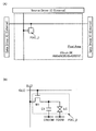
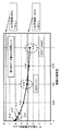
- FIG. 2 is a block diagram showing a display module of Example 1, and a circuit diagram showing a pixel of Example 1.
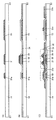
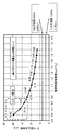
- FIG. FIG. 3 is a top view illustrating a pixel layout of Example 1; The rough result of the data writing time of Example 1. The rough result of the data writing time of Example 1.
- FIG. 2 is a block diagram showing a display module of Example 1, and a circuit diagram showing a pixel of Example 1.
- FIG. 3 is a top view illustrating a pixel layout of Example 1; The rough result of the data writing time of Example 1. The rough result of the data writing time of Example 1. The rough result of the data writing time of Example 1. The rough result of the data writing time of Example 1. The rough result of the data writing time of Example 1. The rough result of the data writing time of Example 1.
- ordinal numbers such as “first” and “second” are used for avoiding confusion between components, and are not limited numerically.
- a transistor is a kind of semiconductor element, and can realize amplification of current and voltage, switching operation for controlling conduction or non-conduction, and the like.
- the transistors in this specification include an IGFET (Insulated Gate Field Effect Transistor) and a thin film transistor (TFT: Thin Film Transistor).
- source and drain may be switched when transistors having different polarities are employed, or when the direction of current changes during circuit operation. Therefore, in this specification, the terms “source” and “drain” can be used interchangeably.
- source may be referred to as “source electrode”, “drain electrode”, and “gate electrode”, respectively.
- “electrically connected” includes a case of being connected via “thing having some electric action”.
- the “thing having some electric action” is not particularly limited as long as it can exchange electric signals between connection targets.
- “things having some electric action” include electrodes, wirings, switching elements such as transistors, resistance elements, coils, capacitive elements, and other elements having various functions.
- a display panel which is one embodiment of a display device has a function of displaying (outputting) an image or the like on a display surface. Therefore, the display panel is one mode of the output device.
- the display panel substrate is attached with a connector such as FPC (Flexible Printed Circuit) or TCP (Tape Carrier Package), or the substrate is integrated with a COG (Chip On Glass) method or the like.
- a connector such as FPC (Flexible Printed Circuit) or TCP (Tape Carrier Package)
- COG Chip On Glass
- the display panel substrate is mounted with a connector such as FPC (Flexible Printed Circuit) or TCP (Tape Carrier Package), or the substrate is integrated with a COG (Chip On Glass) method or the like.
- COG Chip On Glass
- the touch sensor has a function of detecting that a detection target such as a finger or a stylus touches, presses, or approaches. Moreover, you may have the function to detect the positional information. Therefore, the touch sensor is an aspect of the input device.
- the touch sensor can be configured to have one or more sensor elements.
- a substrate having a touch sensor may be referred to as a touch sensor panel or simply a touch sensor.
- a touch sensor panel substrate for example, an FPC or TCP connector attached, or a substrate on which an IC is mounted by a COG method, etc. is referred to as a touch sensor panel module, a touch sensor. It may be called a module, a sensor module, or simply a touch sensor.
- a touch panel that is one embodiment of a display device has a function of displaying (outputting) an image or the like on a display surface, and a detection target such as a finger or a stylus touches, presses, or approaches the display surface. And a function as a touch sensor for detecting the above. Accordingly, the touch panel is an embodiment of an input / output device.
- the touch panel can also be referred to as, for example, a display panel with a touch sensor (or display device) or a display panel with a touch sensor function (or display device).
- the touch panel can be configured to include a display panel and a touch sensor panel.
- the display panel may have a function as a touch sensor inside or on the surface.
- a touch panel substrate a connector such as an FPC or TCP, or an IC mounted on the substrate by a COG method, a touch panel module, a display module, or simply a touch panel is used. And so on.
- One embodiment of the present invention is a display device including a display portion in which a plurality of pixels are arranged in a matrix.
- a wiring to which a selection signal is supplied also referred to as a gate line or a scanning line
- a wiring to which a signal written to a pixel also referred to as a video signal
- a source line, a signal line, a data line, or the like are also provided in plurality.
- the gate lines and the source lines are provided in parallel to each other, and the gate line and the source line intersect each other.
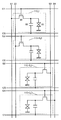
- One pixel includes at least one transistor and one display element.
- the display element includes a conductive layer functioning as a pixel electrode, and the conductive layer is electrically connected to one of a source and a drain of the transistor.
- the gate is electrically connected to the gate line, and the other of the source and the drain is electrically connected to the source line.
- the extending direction of the gate line is referred to as the row direction or the first direction
- the extending direction of the source line is referred to as the column direction or the second direction.
- the same selection signal is supplied to three or more adjacent gate lines. That is, it is preferable that the selection periods of these gate lines be the same. In particular, a set of four gate lines is preferable because the configuration of the drive circuit can be simplified.
- the structure is such that four source lines are arranged for each column.
- one horizontal period can be made longer than the conventional one. For example, when the same selection signal is supplied to four gate lines, the length of one horizontal period can be quadrupled. Furthermore, since the parasitic capacitance between the source lines can be reduced, the load on the source lines can be reduced. Accordingly, even a display device with extremely high resolution such as 4K or 8K can be operated using a transistor with low field-effect mobility. Needless to say, a display device with a resolution exceeding 8K (eg, 10K, 12K, or 16K) can be operated with the structure of one embodiment of the present invention. Further, the above-described configuration can be applied to a large display device having a screen size of 50 inches diagonal or larger, 60 inches diagonal or larger, or 70 inches diagonal or larger.
- two source lines can be arranged on the left side of the pixel and two source lines can be arranged on the right side of the pixel. That is, source lines can be arranged on the left outer side, left inner side, right inner side, and right outer side of the pixel, respectively.
- the source of the transistor electrically connected to the source line on the left outer side of the pixel intersects with the source line on the left inner side of the pixel.
- the source of the transistor electrically connected to the source line on the right outer side of the pixel intersects with the source line on the right inner side of the pixel.
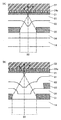
- a conductive layer that can be formed in the same process as a pixel electrode and a conductive layer that can be formed in the same process as a gate of a transistor are used.
- the short circuit between the source of the transistor electrically connected to the line and the left inner source line of the pixel is suppressed.
- a conductive layer that can be formed in the same step as the pixel electrode and a conductive layer that can be formed in the same step as the gate of the transistor are used.
- the short circuit between the source of the transistor electrically connected to the source line and the source line on the right inner side of the pixel is suppressed.
- the configuration is such that four source lines are arranged for each column
- the number of processes more specifically, compared to the configuration where one or two source lines are arranged for each column.
- the increase in the number of photolithography processes can be suppressed. That is, an increase in the number of photomasks can be suppressed. Thereby, an increase in manufacturing cost of the display device can be suppressed.
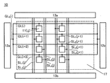
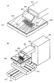
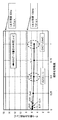
- FIG. 1 is a block diagram of a display device 10 of one embodiment of the present invention.
- the display device 10 includes a display unit 17, a gate driver 12a, a gate driver 12b, a source driver 13a, and a source driver 13b.
- the display unit 17 is provided with pixels 11 in a matrix. Note that in this specification and the like, the pixel 11 in the i-th row and the j-th column is described as a pixel 11 (i, j).
- FIG. 1 shows an example in which the gate driver 12a and the gate driver 12b are provided at positions facing each other with the display unit 17 interposed therebetween.
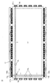
- the gate driver 12a and the gate driver 12b a plurality of wirings GL 0 is connected.
- the wiring GL 0 (i) is shown.
- the wiring GL 0 (i) is electrically connected to four wirings (wiring GL (i), wiring GL (i + 1), wiring GL (i + 2), and wiring GL (i + 3)). Therefore, the same selection signal is given to these four wirings.
- the wiring GL 0 and line GL functions as a gate line.
- the gate driver 12a and the gate driver 12b has a function of supplying the same selection signal to the same line GL 0. This makes it possible to display device 10 than with only one gate driver, shortening the charging and discharging time of the wiring GL 0. Accordingly, even a display device with extremely high resolution such as 4K or 8K can be operated using a transistor with low field-effect mobility.
- the display device of one embodiment of the present invention can be applied to a large display device having a screen size of 50 inches diagonal, 60 inches diagonal, or 70 inches diagonal.
- FIG. 1 illustrates an example in which the source driver 13a and the source driver 13b are provided with the display unit 17 interposed therebetween.
- a plurality of wirings are connected to the source driver 13a and the source driver 13b.
- Four wirings are provided for one pixel column.
- four wirings (wiring SL 1 (j), wiring SL 2 (j), wiring SL 3 (j), wiring SL 4 (j)) corresponding to the j-th pixel column, Four wirings (a wiring SL 1 (j + 1), a wiring SL 2 (j + 1), a wiring SL 3 (j + 1), and a wiring SL 4 (j + 1)) corresponding to the pixel column are illustrated.
- Different signals can be supplied to different wirings.
- different signals can be supplied to the wiring SL 1 (j), the wiring SL 2 (j), the wiring SL 3 (j), and the wiring SL 4 (j).
- the wiring SL (the wiring SL 1 , the wiring SL 2 , the wiring SL 3 , and the wiring SL 4 ) functions as a source line.
- the source driver 13a and the source driver 13b have a function of supplying the same signal to the same wiring SL. Thereby, the charge / discharge time of the wiring SL can be shortened compared with the case where the display device 10 has only one source driver. Accordingly, even a display device with extremely high resolution such as 4K or 8K can be operated using a transistor with low field-effect mobility.
- the display device of one embodiment of the present invention can be applied to a large display device having a screen size of 50 inches diagonal, 60 inches diagonal, or 70 inches diagonal.
- One pixel 11 is a pixel corresponding to one color. Therefore, in the case where color display is performed using a color mixture of light exhibited by a plurality of pixels, the pixel 11 can also be referred to as a sub-pixel.
- the plurality of pixels arranged in a line in the column direction are preferably pixels that exhibit the same color.
- a pixel layer arranged in a line in the column direction is provided with a colored layer that overlaps with the liquid crystal element and transmits the same color light.
- the display portion of the display device can be driven by being divided into a plurality of display regions.
- the boundary portion of the divided display area may be visually recognized due to variations in characteristics of the drive circuit, and visibility may be deteriorated.
- image processing or the like for dividing input image data in advance is required, and a high-speed and large-scale image processing apparatus is required.
- the display device of one embodiment of the present invention can be driven without dividing the display portion into a plurality of display regions even when a transistor with relatively low field-effect mobility is used.
- the display device 10 may be provided with a protection circuit.
- FIG. 2 is a block diagram of the display device 10 when the display device 10 having the configuration shown in FIG. 1 is provided with a protection circuit 18a, a protection circuit 18b, a protection circuit 19a, and a protection circuit 19b. Protection circuit 18a and the protection circuit 18b, the wiring GL 0 and are electrically connected. Protection circuit 19a and the protection circuit 19b, the wiring SL 1, line SL 2, lines SL 3, and the wiring SL 4 are electrically connected to the.
- the protection circuit 18a can be provided on the gate driver 12a side, and the protection circuit 18b can be provided on the gate driver 12b side. That is, the protection circuit 18a and the protection circuit 18b can be provided at positions facing each other with the display unit 17 interposed therebetween.
- the protection circuit 19a can be provided on the source driver 13a side, and the protection circuit 19b can be provided on the source driver 13b side. That is, the protection circuit 19a and the protection circuit 19b can be provided at positions facing each other with the display unit 17 interposed therebetween.
- the pixel 11 can be protected from noise, surge, electrostatic discharge, or the like. Thereby, the reliability of the display apparatus 10 can be improved.
- FIG. 3 illustrates a configuration in which three source lines (a wiring SL 1 , a wiring SL 2 , and a wiring SL 3 ) are provided per pixel column.
- the wiring GL 0 (i) is electrically connected to three wirings (the wiring GL (i), the wiring GL (i + 1), and the wiring GL (i + 2)).
- the same selection signal is given to the wiring. Note that in one embodiment of the present invention, five or more source lines may be provided per pixel column.
- FIG. 1 shows an example in which two gate drivers and two source drivers are arranged, only one or both of the gate driver and the source driver may be arranged.
- FIG. 4 shows an example in which one source driver 13a and one source driver 13b are arranged for each pixel column. That is, the same number of source drivers 13 a as the pixel columns are provided along one side of the rectangular display unit 17, and the same number of source drivers 13 b as the pixel columns are provided at positions facing the source driver 13 a and the display unit 17. It is done. Further, FIG. 4 shows an example of a gate driver 12a and the gate driver 12b, and arranged one by one per line GL 0 of one, respectively. In other words, the number of gate drivers 12 a obtained by dividing the pixel row by 4 is provided along one side of the rectangular display unit 17, and the pixel row is divided by 4 at a position facing the gate driver 12 a and the display unit 17. A number of gate drivers 12b are provided. With such a structure, display unevenness due to a potential drop caused by wiring resistance can be reduced even in a large display device.
- the display device 10 can be provided with a reference voltage generation circuit.
- the reference voltage generation circuit has a function of generating a reference voltage of a signal supplied from the source driver.
- a reference voltage generation circuit for example, a gamma reference generation circuit can be used.
- FIG. 5 shows a reference voltage generation circuit 16a having a function of supplying a reference voltage to the source driver 13a and a reference voltage generation circuit having a function of supplying a reference voltage to the source driver 13b in the display device 10 having the configuration shown in FIG. 16b are provided.
- FIG. 6 shows a case where the display device 10 having the configuration shown in FIG. 4 is provided with a reference voltage generation circuit 16 having a function of supplying a reference voltage to the source driver 13a and the source driver 13b. Even when the display device 10 has the configuration shown in FIG. 6, the accuracy of the voltage of the signal generated from each source driver 13a and the accuracy of the voltage of the signal generated from each source driver 13b can be improved. .
- a circuit diagram including this is shown.
- One pixel 11 includes a transistor 30, a liquid crystal element 20, and a capacitor element 60.
- the wirings S1 to S4 each correspond to a source line, and the wirings G1 to G4 each correspond to a gate line.
- the wiring S1 corresponds to the wiring SL 1 (j)
- the wiring S2 corresponds to the wiring SL 2 (j)
- the wiring S3 corresponds to the wiring SL 3 (j)
- the wiring S4. Corresponds to the wiring SL 4 (j).
- the wiring G1 corresponds to the wiring GL (i)
- the wiring G2 corresponds to the wiring GL (i + 1)
- the wiring G3 corresponds to the wiring GL (i + 2)
- the wiring G4 corresponds to the wiring GL.
- a wiring S1 is electrically connected to one of a source and a drain of the transistor 30 included in the pixel 11 (i, j), and a wiring G1 is electrically connected to the gate of the transistor 30 included in the pixel 11 (i, j).
- a wiring S2 is electrically connected to one of a source and a drain of the transistor 30 included in the pixel 11 (i + 1, j), and a wiring G2 is electrically connected to the gate of the transistor 30 included in the pixel 11 (i + 1, j). Connected to.
- a wiring S3 is electrically connected to one of a source and a drain of the transistor 30 included in the pixel 11 (i + 2, j), and a wiring G3 is electrically connected to the gate of the transistor 30 included in the pixel 11 (i + 2, j).
- a wiring S4 is electrically connected to one of a source and a drain of the transistor 30 included in the pixel 11 (i + 3, j), and a wiring G4 is electrically connected to the gate of the transistor 30 included in the pixel 11 (i + 3, j). Connected to.
- the other of the source and the drain of the transistor 30 is electrically connected to one electrode of the capacitor 60 and one electrode (pixel electrode) of the liquid crystal element 20.
- a wiring CS is electrically connected to the other electrode of the capacitor 60, and a common potential is supplied to the wiring CS.
- the transistor 30 has a function of controlling writing of a signal supplied from the source line to the pixel 11 by switching between an on state and an off state. Specifically, when the transistor 30 is turned on, electric charge corresponding to a signal supplied from the source line can be written to the capacitor 60 electrically connected to the transistor 30. Further, the charge written in the capacitor 60 can be held by turning off the transistor 30.
- the transistor 30 can be a transistor using amorphous silicon.
- a transistor using amorphous silicon has difficulty in increasing field-effect mobility
- the display device of one embodiment of the present invention has an extremely high value of 4K, 8K, or the like even when such a transistor is used. It can be a resolution.
- a large display device with a screen size of 50 inches or more, 60 inches or more, or 70 inches or more can be provided.
- the transistor 30 can be a transistor including a metal oxide in a channel formation region (hereinafter also referred to as an OS transistor).
- a metal oxide has a larger energy gap than a semiconductor such as silicon, and an OS transistor can have a low minority carrier density. Therefore, when the OS transistor is in an off state, a current flowing between the source and the drain of the OS transistor (hereinafter also referred to as an off current) is extremely small. Therefore, by using an OS transistor as the transistor 30, electric charge can be held in the capacitor 60 for a long time. Thereby, the frequency of charge writing into the capacitor element 60, that is, the frequency of the refresh operation can be reduced, and the power consumption of the display device 10 can be reduced.
- a metal oxide is a metal oxide in a broad expression.
- Metal oxides are classified into oxide insulators, oxide conductors (including transparent oxide conductors), and oxide semiconductors (also referred to as oxide semiconductors or simply OS).
- oxide semiconductors also referred to as oxide semiconductors or simply OS.
- the metal oxide may be referred to as an oxide semiconductor. That is, when a metal oxide has at least one of an amplifying function, a rectifying function, and a switching function, the metal oxide can be referred to as a metal oxide semiconductor, or OS for short.
- OS FET refers to a transistor including a metal oxide or an oxide semiconductor.
- metal oxides containing nitrogen may be collectively referred to as metal oxides.
- a metal oxide containing nitrogen may be referred to as a metal oxynitride.
- CAAC c-axis aligned crystal
- CAC Cloud-aligned Composite
- a CAC-OS or a CAC-metal oxide has a conductive function in part of a material and an insulating function in part of the material, and the whole material is a semiconductor. It has the function of.
- the conductive function is a function of flowing electrons (or holes) serving as carriers
- the insulating function is an electron serving as carriers. It is a function that does not flow.
- a function of switching (a function of turning on / off) can be imparted to CAC-OS or CAC-metal oxide by causing the conductive function and the insulating function to act complementarily.
- CAC-OS or CAC-metaloxide the functions of both can be maximized by separating the functions.
- CAC-OS or CAC-metal oxide includes a conductive region and an insulating region.
- the conductive region has the above-described conductive function
- the insulating region has the above-described insulating function.
- the conductive region and the insulating region may be separated at the nanoparticle level.
- the conductive region and the insulating region may be unevenly distributed in the material, respectively.
- the conductive region may be observed with the periphery blurred and connected in a cloud shape.
- the conductive region and the insulating region are dispersed in the material with a size of 0.5 nm to 10 nm, preferably 0.5 nm to 3 nm, respectively. There is.
- CAC-OS or CAC-metal oxide is composed of components having different band gaps.
- CAC-OS or CAC-metal oxide includes a component having a wide gap caused by an insulating region and a component having a narrow gap caused by a conductive region.
- the carrier when the carrier flows, the carrier mainly flows in the component having the narrow gap.
- the component having a narrow gap acts in a complementary manner to the component having a wide gap, and the carrier flows through the component having the wide gap in conjunction with the component having the narrow gap. Therefore, when the CAC-OS or the CAC-metal oxide is used for a channel formation region of a transistor, high current driving force, that is, high on-state current and high field-effect mobility can be obtained in the on-state of the transistor.
- CAC-OS or CAC-metal oxide can also be called a matrix composite material (metal matrix composite) or a metal matrix composite material (metal matrix composite).
- FIG. 8A shows an example of the layout of the pixel 11 (i + 2, j) and the pixel 11 (i + 3, j).
- FIG. 8A and the like the same hatching is given to the components provided in the same layer.
- the same hatching may be given to the components provided in the same layer.
- the wiring G3, the wiring G4, and the wiring CS extend in the row direction (lateral direction), and the wirings S1 to S4 extend in the column direction (vertical direction).
- the semiconductor layer 32 is provided over the wiring G3, and part of the wiring G3 functions as a gate. Further, part of the wiring S3 functions as one of a source and a drain.
- the semiconductor layer 32 has a region located between the wiring S2 and the wiring S3.
- a conductive layer 33 a that functions as the other of the source and the drain of the transistor 30 and one electrode of the capacitor 60 is provided so as to be electrically connected to the semiconductor layer 32.
- a conductive layer 21 having a function as a pixel electrode is provided, and the conductive layer 33 a and the conductive layer 21 are electrically connected through the opening 38.
- the semiconductor layer 32 is provided over the wiring G4, and part of the wiring G4 functions as a gate.
- the semiconductor layer 32 has a region located between the wiring S2 and the wiring S3.
- a conductive layer 33 a that functions as the other of the source and the drain of the transistor 30 and one electrode of the capacitor 60 is provided so as to be electrically connected to the semiconductor layer 32.
- a conductive layer 21 having a function as a pixel electrode is provided, and the conductive layer 33 a and the conductive layer 21 are electrically connected through the opening 38.
- a conductive layer 51 that functions as one of a source and a drain of the transistor 30 is provided so as to be electrically connected to the semiconductor layer 32.
- the conductive layer 51 is electrically connected to the conductive layer 52 formed in the same layer as the conductive layer 21 through the opening 71.
- the conductive layer 52 is electrically connected to the conductive layer 53 formed in the same layer as the wiring G4 through the opening 72.
- the conductive layer 53 is electrically connected to the conductive layer 54 formed in the same layer as the conductive layer 21 through the opening 73.
- the conductive layer 54 is electrically connected to the wiring S4 through the opening 74.
- the conductive layer 51 functioning as one of the source and the drain of the transistor 30 is electrically connected to the wiring S4 through the conductive layer 52, the conductive layer 53, and the conductive layer 54. It is connected.
- the conductive layer 51, the wiring S3, and the wiring S4 are provided in the same layer, and the conductive layer 53 has a region overlapping with the wiring S3. The one of the source and the drain of the transistor 30 can be prevented from being short-circuited with the wiring S3.
- the conductive layer 52 and the conductive layer 54 can be formed in the same step as the conductive layer 21 having a function as a pixel electrode, and the conductive layer 53 can be formed in the same step as the wiring G4.
- the number of processes more specifically, compared to the configuration where one or two source lines are arranged for each column.
- the increase in the number of photolithography processes can be suppressed. That is, an increase in the number of photomasks can be suppressed. Thereby, an increase in manufacturing cost of the display device can be suppressed.
- FIG. 8B shows an example of the layout of the pixel 11 (i, j) and the pixel 11 (i + 1, j). As shown in FIG. 8B, the wiring G1 and the wiring G2 extend in the row direction.
- the conductive layer 51 that functions as one of the source and the drain of the transistor 30 is electrically connected to the wiring S1 through the conductive layer 52, the conductive layer 53, and the conductive layer 54. ing. In other respects, the configuration of the pixel 11 (i, j) and the configuration of the pixel 11 (i + 3, j) are the same.
- part of the wiring S2 functions as one of the source and the drain of the transistor 30.
- the configuration of the pixel 11 (i + 1, j) and the configuration of the pixel 11 (i + 2, j) are the same.
- FIG. 9 shows an example of a cross section corresponding to the cutting line A1-A2 in FIG.
- a transmissive liquid crystal element 20 is applied as a display element is shown.
- the substrate 15 side is the display surface side.
- the display device 10 has a configuration in which a liquid crystal 22 is sandwiched between a substrate 14 and a substrate 15.
- the liquid crystal element 20 includes a conductive layer 21 provided on the substrate 14 side, a conductive layer 23 provided on the substrate 15 side, and a liquid crystal 22 sandwiched therebetween.
- An alignment film 24 a is provided between the liquid crystal 22 and the conductive layer 21, and an alignment film 24 b is provided between the liquid crystal 22 and the conductive layer 23.
- the conductive layer 21 has a function as a pixel electrode. Further, the conductive layer 23 functions as a common electrode or the like. Further, each of the conductive layer 21 and the conductive layer 23 has a function of transmitting visible light. Therefore, the liquid crystal element 20 is a transmissive liquid crystal element.
- a colored layer 41 and a light shielding layer 42 are provided on the surface of the substrate 15 on the substrate 14 side.
- An insulating layer 26 is provided so as to cover the colored layer 41 and the light shielding layer 42, and a conductive layer 23 is provided so as to cover the insulating layer 26.
- the colored layer 41 is provided in a region overlapping with the conductive layer 21.
- the light shielding layer 42 is provided so as to cover the transistor 30 and the opening 38.
- a polarizing plate 39 a is disposed outside the substrate 14, and a polarizing plate 39 b is disposed outside the substrate 15. Further, a backlight unit 90 is provided outside the polarizing plate 39a.
- a transistor 30, a capacitor element 60, and the like are provided over the substrate 14.
- the transistor 30 has a function as a selection transistor of the pixel 11.
- the transistor 30 is electrically connected to the liquid crystal element 20 through the opening 38.
- the transistor 30 shown in FIG. 9 is a so-called bottom-gate / channel-etched transistor.
- the transistor 30 includes a conductive layer 31 functioning as a gate, an insulating layer 34 functioning as a gate insulating layer, a semiconductor layer 32, and a pair of impurity semiconductor layers 35 functioning as a source region and a drain region. And a pair of conductive layers 33a and 33b having a function as a source and a drain.
- a portion of the semiconductor layer 32 that overlaps with the conductive layer 31 functions as a channel formation region.
- the impurity semiconductor layer 35 is provided in contact with the semiconductor layer 32, and the conductive layer 33 a and the conductive layer 33 b are provided in contact with the impurity semiconductor layer 35.
- the impurity semiconductor layer may be simply referred to as a semiconductor layer.
- the conductive layer 31 corresponds to part of the wiring G3 in FIG. 8A
- the conductive layer 33b corresponds to part of the wiring S3.
- a conductive layer 31a and a conductive layer 33c described later correspond to a part of the wiring CS and a part of the wiring S4, respectively.
- the semiconductor layer 32 is preferably a semiconductor containing silicon.
- amorphous silicon, microcrystalline silicon, polycrystalline silicon, or the like can be used.
- amorphous silicon is preferably used because it can be formed over a large substrate with a high yield.
- the display device of one embodiment of the present invention can perform favorable display even when a transistor to which amorphous silicon with relatively low field-effect mobility is used is used.
- the impurity semiconductor layer 35 is formed using a semiconductor to which an impurity element imparting one conductivity type is added.
- a semiconductor to which an impurity element imparting one conductivity type is added includes, for example, silicon to which P or As is added.
- B can be added as the impurity element imparting one conductivity type, but the transistor is preferably n-type.
- the impurity semiconductor layer 35 may be formed using an amorphous semiconductor or a crystalline semiconductor such as a microcrystalline semiconductor.
- the capacitive element 60 includes a conductive layer 31a, an insulating layer 34, and a conductive layer 33a.
- a conductive layer 33 c is provided on the conductive layer 31 with an insulating layer 34 interposed therebetween.
- An insulating layer 82 and an insulating layer 81 are stacked so as to cover the transistor 30 and the like.
- the conductive layer 21 having a function as a pixel electrode is provided over the insulating layer 81. Further, the conductive layer 21 and the conductive layer 33 a are electrically connected through the opening 38 provided in the insulating layer 81 and the insulating layer 82.
- the insulating layer 81 preferably has a function as a planarization layer.
- the insulating layer 82 preferably has a function as a protective film that suppresses diffusion of impurities and the like into the transistor 30 and the like.
- an inorganic insulating material can be used for the insulating layer 82 and an organic insulating material can be used for the insulating layer 81.
- the insulating layer 82 and the insulating layer 81 may be collectively regarded as one insulating layer.
- FIG. 10 shows an example of a cross section corresponding to the cutting line B1-B2 in FIG. 10 includes a conductive layer 31 functioning as a gate, an insulating layer 34 functioning as a gate insulating layer, a semiconductor layer 32, and a pair of impurities functioning as a source region and a drain region.
- the semiconductor layer 35 includes a pair of conductive layers 33 a and a conductive layer 51 that function as a source and a drain.
- a portion of the semiconductor layer 32 that overlaps with the conductive layer 31 functions as a channel formation region.
- the impurity semiconductor layer 35 is provided in contact with the semiconductor layer 32, and the conductive layer 33 a and the conductive layer 51 are provided in contact with the impurity semiconductor layer 35.
- the conductive layer 31 corresponds to part of the wiring G4 in FIG.
- the conductive layer 31a, the conductive layer 33b, and the conductive layer 33c correspond to a part of the wiring CS, a part of the wiring S3, and a part of the wiring S4, respectively.
- the conductive layer 33 b is provided so as to have a region overlapping with the conductive layer 53 with the insulating layer 34 interposed therebetween.
- the conductive layer 51 and the conductive layer 52 are electrically connected through the opening 71 provided in the insulating layer 81 and the insulating layer 82.
- the conductive layer 52 and the conductive layer 53 are electrically connected through the insulating layer 81, the insulating layer 82, and the opening 72 provided in the insulating layer 34.
- the conductive layer 53 and the conductive layer 54 are electrically connected through the insulating layer 81, the insulating layer 82, and the opening 73 provided in the insulating layer 34.
- the conductive layer 54 and the conductive layer 33 c are electrically connected through an opening 74 provided in the insulating layer 81 and the insulating layer 82.
- the layer 33c is electrically connected.
- the opening 72 and the opening 73 are formed with the conductive layer 33b interposed therebetween.
- the conductive layer 51 functioning as one of the source and the drain of the transistor 30 is suppressed from being short-circuited with the conductive layer 33b corresponding to part of the wiring S3.
- the conductive layer 52 and the conductive layer 54 are formed in the same layer as the conductive layer 21, and the conductive layer 53 is formed in the same layer as the conductive layer 31 and the conductive layer 31a. ing.
- the components formed in the same layer can have the same material. That is, for example, the conductive layer 21, the conductive layer 52, and the conductive layer 54 can each have the same material. Further, for example, the conductive layer 31, the conductive layer 31a, and the conductive layer 53 can each have the same material.
- FIG. 11 shows a modification of the configuration shown in FIG.
- FIG. 11 shows an example in which the colored layer 41 is provided on the substrate 14 side. Thereby, the structure by the side of the board
- the insulating layer 81 may not be provided. Thereby, the number of manufacturing steps of the display device 10 can be reduced, and the manufacturing cost of the display device 10 can be reduced.
- FIG. 12 shows a modification of the configuration shown in FIG. FIG. 12 illustrates an example in which the conductive layer 52, the conductive layer 53, the conductive layer 54, the opening 72, and the opening 73 are omitted.
- the conductive layer 51 and the conductive layer 33 c are electrically connected via the conductive layer 55 formed in the same layer as the conductive layer 21.
- the conductive layer 51 and the conductive layer 55 are electrically connected through the opening 71
- the conductive layer 33 c and the conductive layer 55 are electrically connected through the opening 74.
- FIG. 13 shows a modification of the configuration shown in FIG. 9, FIG. 14 shows a modification of the configuration shown in FIG. 10, FIG. 15 shows a modification of the configuration shown in FIG. 11, FIG. Each modification of the configuration is shown.
- the configuration shown in FIGS. 13 to 16 is different from the configuration shown in FIGS. 9 to 12 in that the impurity semiconductor layer 35 is not provided.
- a semiconductor containing a metal oxide for the semiconductor layer 32 it is preferable to use a semiconductor containing a metal oxide for the semiconductor layer 32.
- a semiconductor containing a metal oxide for the semiconductor layer 32 that is, by using the transistor 30 as an OS transistor, the charge corresponding to the signal supplied from the source line is held in the capacitor 60 for a long time as described above. be able to.
- the frequency of charge writing into the capacitor element 60 that is, the frequency of the refresh operation can be reduced, and the power consumption of the display device 10 can be reduced.
- a substrate having a flat surface can be used for the substrate included in the display panel.
- a substrate that extracts light from the display element is formed using a material that transmits the light.
- materials such as glass, quartz, ceramic, sapphire, and organic resin can be used.
- the display panel can be reduced in weight and thickness.
- a flexible display panel can be realized by using a flexible substrate.
- glass that is thin enough to be flexible can be used for the substrate.
- a composite material in which glass and a resin material are bonded to each other with an adhesive layer may be used.
- the transistor includes a conductive layer having a function as a gate, a semiconductor layer, a conductive layer having a function as a source, a conductive layer having a function as a drain, and an insulating layer having a function as a gate insulating layer.
- the structure of the transistor included in the display device of one embodiment of the present invention there is no particular limitation on the structure of the transistor included in the display device of one embodiment of the present invention.
- a planar transistor, a staggered transistor, or an inverted staggered transistor may be used.
- a top-gate or bottom-gate transistor structure may be employed.
- gates may be provided above and below the channel.
- crystallinity of the semiconductor layer used for the transistor there is no particular limitation on the crystallinity of the semiconductor layer used for the transistor, and any of an amorphous semiconductor and a semiconductor having crystallinity (a microcrystalline semiconductor, a polycrystalline semiconductor, a single crystal semiconductor, or a semiconductor partially including a crystal region) can be used. It may be used. It is preferable to use a crystalline semiconductor because deterioration of transistor characteristics can be suppressed.
- an element belonging to Group 14 can be used for the semiconductor layer of the transistor.
- silicon it is particularly preferable to use amorphous silicon as the silicon.
- amorphous silicon By using amorphous silicon, a transistor can be formed over a large substrate with high yield, so that the mass productivity of the display device of one embodiment of the present invention can be increased.
- crystalline silicon such as microcrystalline silicon, polycrystalline silicon, or single crystal silicon can be used.
- polycrystalline silicon can be formed at a lower temperature than single crystal silicon, and has higher field effect mobility and higher reliability than amorphous silicon.
- the bottom-gate transistor described in this embodiment is preferable because the number of manufacturing steps can be reduced.
- amorphous silicon can be used at a lower temperature than polycrystalline silicon, it is possible to use a material having low heat resistance as a material for wiring, electrodes, and substrates below the semiconductor layer. Can widen the choice of materials. For example, a glass substrate having a very large area can be suitably used.
- a top-gate transistor is preferable because an impurity region can be easily formed in a self-aligning manner and variation in characteristics can be reduced. In this case, it may be particularly suitable when polycrystalline silicon, single crystal silicon, or the like is used.
- a metal oxide can be used for a semiconductor layer of the transistor.
- a semiconductor containing silicon, a semiconductor containing gallium arsenide, a metal oxide containing indium, or the like can be used.
- a metal oxide having a larger band gap than silicon it is preferable to use a metal oxide having a larger band gap than silicon. It is preferable to use a semiconductor material having a wider band gap and lower carrier density than silicon because current in the off-state of the transistor can be reduced.
- a transistor using a metal oxide having a band gap larger than that of silicon can hold charge accumulated in a capacitor connected in series with the transistor for a long time because of the low off-state current.
- the driving circuit can be stopped while maintaining the gradation of an image displayed on each display portion. As a result, a display device with extremely reduced power consumption can be realized.
- the semiconductor layer is represented by an In-M-Zn-based oxide containing at least indium, zinc, and M (metal such as aluminum, titanium, gallium, germanium, yttrium, zirconium, lanthanum, cerium, tin, neodymium, or hafnium). It is preferable to include a film. In addition, in order to reduce variation in electric characteristics of a transistor including the semiconductor layer, a stabilizer is preferably included together with the transistor.
- Examples of the stabilizer include the metals described in M above, and examples include gallium, tin, hafnium, aluminum, and zirconium.
- Other stabilizers include lanthanoids such as lanthanum, cerium, praseodymium, neodymium, samarium, europium, gadolinium, terbium, dysprosium, holmium, erbium, thulium, ytterbium, and lutetium.
- an In—Ga—Zn-based oxide means an oxide containing In, Ga, and Zn as its main components, and there is no limitation on the atomic ratio of In, Ga, and Zn.
- the semiconductor layer and the conductive layer may have the same metal element among the above oxides.
- Manufacturing costs can be reduced by using the same metal element for the semiconductor layer and the conductive layer.
- the manufacturing cost can be reduced by using metal oxide targets having the same metal composition.
- an etching gas or an etching solution for processing the semiconductor layer and the conductive layer can be used in common.
- the semiconductor layer and the conductive layer may have different compositions even if they have the same metal element. For example, a metal element in a film may be detached during a manufacturing process of a transistor and a capacitor to have a different metal composition.
- the metal oxide constituting the semiconductor layer preferably has an energy gap of 2 eV or more, preferably 2.5 eV or more, more preferably 3 eV or more. In this manner, off-state current of a transistor can be reduced by using a metal oxide having a wide energy gap.
- the atomic ratio of the metal elements of the sputtering target used for forming the In-M-Zn oxide satisfies In ⁇ M. Is preferred.
- the atomic ratio of the metal element contained in the semiconductor layer to be deposited includes a variation of plus or minus 40% of the atomic ratio of the metal element contained in
- the metal oxide constituting the semiconductor layer is preferably a CAC-OS or a CAC-metal oxide described later.
- the field effect mobility of the transistor can be increased.
- the semiconductor layer has a carrier density of 1 ⁇ 10 17 / cm 3 or less, preferably 1 ⁇ 10 15 / cm 3 or less, more preferably 1 ⁇ 10 13 / cm 3 or less, more preferably 1 ⁇ 10 11 / cm 3. 3 or less, more preferably less than 1 ⁇ 10 10 / cm 3 , and a metal oxide of 1 ⁇ 10 ⁇ 9 / cm 3 or more can be used.
- a semiconductor layer has stable characteristics because it has a low impurity concentration and a low density of defect states.
- examples of the impurity include water and hydrogen.
- a metal oxide having a low impurity concentration and a low density of defect states may be referred to as a highly pure intrinsic metal oxide or a substantially highly purified intrinsic metal oxide.
- a transistor including the metal oxide rarely has electrical characteristics (also referred to as normally-on) in which the threshold voltage is negative.
- a metal oxide that is highly purified intrinsic or substantially highly purified intrinsic has a low defect level density, and thus may have a low trap level density.
- a transistor including a metal oxide having high purity intrinsic or substantially high purity intrinsic has an extremely small off-current, an element having a channel width W of 1 ⁇ 10 6 ⁇ m and a channel length L of 10 ⁇ m.
- the off-state current can be less than the measurement limit of the semiconductor parameter analyzer, that is, 1 ⁇ 10 ⁇ 13 A or less.
- a semiconductor layer that can be used in one embodiment of the present invention is not limited to the above, and a material having an appropriate composition can be used depending on required semiconductor characteristics and electrical characteristics (field-effect mobility, threshold voltage, and the like) of a transistor Use it.
- a semiconductor layer carrier density, impurity concentration, defect density, atomic ratio of metal element to oxygen, interatomic distance, density, and the like it is preferable to set the semiconductor layer carrier density, impurity concentration, defect density, atomic ratio of metal element to oxygen, interatomic distance, density, and the like to appropriate values. .
- the concentration of silicon or carbon in the semiconductor layer is 2 ⁇ 10 18 atoms / cm 3 or less, preferably 2 ⁇ 10 17 atoms / cm 3 or less. preferable.
- the concentration of alkali metal or alkaline earth metal obtained by secondary ion mass spectrometry in the semiconductor layer is set to 1 ⁇ 10 18 atoms / cm 3 or less, preferably 2 ⁇ 10 16 atoms / cm 3 or less. preferable.
- the semiconductor layer may have a non-single crystal structure, for example.
- the non-single crystal structure includes, for example, a polycrystalline structure, a microcrystalline structure, or an amorphous structure.
- the amorphous structure has the highest density of defect states.
- a metal oxide having an amorphous structure has, for example, disordered atomic arrangement and no crystal component.
- an amorphous oxide film has, for example, a completely amorphous structure and does not have a crystal part.
- the semiconductor layer may be a mixed film including two or more of an amorphous structure region, a microcrystalline structure region, a polycrystalline structure region, and a single crystal structure region.
- the mixed film may have a single-layer structure or a stacked structure including any two or more of the above-described regions.
- Conductive layer In addition to the gate, source, and drain of a transistor, materials that can be used for conductive layers such as various wirings and electrodes constituting a display device include aluminum, titanium, chromium, nickel, copper, yttrium, zirconium, molybdenum, silver, A metal such as tantalum or tungsten, or an alloy containing this as a main component can be used. A film containing any of these materials can be used as a single layer or a stacked structure.
- Two-layer structure to stack, two-layer structure to stack copper film on titanium film, two-layer structure to stack copper film on tungsten film, titanium film or titanium nitride film, and aluminum film or copper film on top of it A three-layer structure for forming a titanium film or a titanium nitride film thereon, a molybdenum film or a molybdenum nitride film, and an aluminum film or a copper film stacked thereon, and a molybdenum film or a There is a three-layer structure for forming a molybdenum nitride film.
- an oxide such as indium oxide, tin oxide, or zinc oxide may be used. Further, it is
- a light-transmitting conductive material that can be used for conductive layers such as various wirings and electrodes constituting a display device includes indium oxide, indium tin oxide, A conductive oxide such as indium zinc oxide, zinc oxide, zinc oxide to which gallium is added, or graphene can be used.
- a metal material such as gold, silver, platinum, magnesium, nickel, tungsten, chromium, molybdenum, iron, cobalt, copper, palladium, or titanium, or an alloy material containing the metal material can be used.
- a nitride (eg, titanium nitride) of the metal material may be used.
- a metal material or an alloy material (or a nitride thereof)
- it may be thin enough to have a light-transmitting property.
- a stacked film of the above materials can be used as a conductive layer.
- a laminated film of an alloy of silver and magnesium and indium tin oxide because the conductivity can be increased.
- conductive layers such as various wirings and electrodes constituting the display device and conductive layers (conductive layers having a function as a pixel electrode or a common electrode) included in the display element.
- Insulating materials that can be used for each insulating layer include, for example, resins such as acrylic and epoxy, resins having a siloxane bond, and inorganic insulation such as silicon oxide, silicon oxynitride, silicon nitride oxide, silicon nitride, and aluminum oxide. Materials can also be used.
- the insulating layer having a region in contact with the semiconductor layer preferably includes a region containing oxygen in excess of the stoichiometric composition (excess oxygen region).
- the insulating layer 34 and the insulating layer 82 having a region in contact with the semiconductor layer 32 preferably have an excess oxygen region. Thereby, oxygen can be supplied from the insulating layer 34 and the insulating layer 82 to the semiconductor layer 32.
- the semiconductor layer 32 includes a metal oxide
- when oxygen vacancies are formed in the metal oxide electrons such as carriers may be generated due to impurities such as hydrogen entering the oxygen vacancies. As a result, the electrical characteristics of the transistor may deteriorate.
- the insulating layer having a region in contact with the semiconductor layer has an excess oxygen region
- oxygen can be supplied from the insulating layer to the semiconductor layer, so that oxygen vacancies can be compensated. Thereby, deterioration of the electrical characteristics of the transistor can be suppressed.
- the insulating layer may be formed in an oxygen atmosphere.
- the insulating layer after deposition may be heat-treated in an oxygen atmosphere.
- liquid crystal element for example, a liquid crystal element to which a vertical alignment (VA: Vertical Alignment) mode is applied can be used.
- VA Vertical Alignment
- MVA Multi-Domain Vertical Alignment
- PVA Power Planed Vertical Alignment
- ASV Advanced Super View
- liquid crystal elements to which various modes are applied can be used.
- VA mode Transmission Nematic
- IPS In-Plane-Switching
- FFS Ringe Field Switching
- ASM Analy Symmetrical Aligned Micro-cell
- a liquid crystal element is an element that controls transmission or non-transmission of light by an optical modulation action of liquid crystal.
- the optical modulation action of the liquid crystal is controlled by an electric field applied to the liquid crystal (including a horizontal electric field, a vertical electric field, or an oblique electric field).
- a thermotropic liquid crystal a low molecular liquid crystal
- a polymer liquid crystal a polymer dispersed liquid crystal
- PNLC polymer network type liquid crystal
- Ferroelectric liquid crystals antiferroelectric liquid crystals, and the like can be used.
- These liquid crystal materials exhibit a cholesteric phase, a smectic phase, a cubic phase, a chiral nematic phase, an isotropic phase, and the like depending on conditions.
- liquid crystal material either a positive type liquid crystal or a negative type liquid crystal may be used, and an optimal liquid crystal material may be used according to an applied mode or design.
- An alignment film can be provided to control the alignment of the liquid crystal.
- liquid crystal exhibiting a blue phase for which an alignment film is unnecessary may be used.
- the blue phase is one of the liquid crystal phases.
- a liquid crystal composition mixed with several percent by weight or more of a chiral agent is used for the liquid crystal layer in order to improve the temperature range.
- a liquid crystal composition containing a liquid crystal exhibiting a blue phase and a chiral agent has a short response speed and is optically isotropic.
- a liquid crystal composition including a liquid crystal exhibiting a blue phase and a chiral agent does not require alignment treatment and has a small viewing angle dependency. Further, since it is not necessary to provide an alignment film, a rubbing process is not required, so that electrostatic breakdown caused by the rubbing process can be prevented, and defects or breakage of the liquid crystal display device during the manufacturing process can be reduced. .
- liquid crystal element examples include a transmissive liquid crystal element, a reflective liquid crystal element, and a transflective liquid crystal element.
- a transmissive liquid crystal element can be particularly preferably used.
- two polarizing plates are provided so as to sandwich a pair of substrates.
- a backlight is provided outside the polarizing plate.
- the backlight may be a direct type backlight or an edge light type backlight. It is preferable to use a direct type backlight having an LED (Light Emitting Diode) because local dimming is facilitated and contrast can be increased.
- An edge light type backlight is preferably used because the thickness of the module including the backlight can be reduced.
- see-through display can be performed by turning off the edge-light type backlight.
- Examples of materials that can be used for the colored layer include metal materials, resin materials, resin materials containing pigments or dyes, and the like.
- the light shielding layer examples include carbon black, titanium black, metal, metal oxide, and composite oxide containing a solid solution of a plurality of metal oxides.
- the light shielding layer may be a film containing a resin material or a thin film of an inorganic material such as a metal.
- a stacked film of a film containing a material for the colored layer can be used for the light shielding layer.
- a stacked structure of a film including a material used for a colored layer that transmits light of a certain color and a film including a material used for a colored layer that transmits light of another color can be used. It is preferable to form the colored layer and the light shielding layer with the same material because the same apparatus can be used and the process can be simplified.
- the thin films (insulating film, semiconductor film, conductive film, etc.) constituting the display device are respectively formed by sputtering, chemical vapor deposition (CVD), vacuum deposition, and pulsed laser deposition (PLD: Pulsed Laser Deposition).
- CVD chemical vapor deposition
- PLD Pulsed Laser Deposition
- Method atomic layer deposition
- ALD Atomic Layer Deposition
- CVD method include a plasma enhanced chemical vapor deposition (PECVD) method and a thermal CVD method.
- An example of the thermal CVD method is a metal organic chemical vapor deposition (MOCVD) method.
- the thin films (insulating film, semiconductor film, conductive film, etc.) constituting the display device are spin coating, dip, spray coating, ink jet printing, dispensing, screen printing, offset printing, etc., or doctor knife, slit coating, It can be formed by roll coating, curtain coating, or knife coating.
- a thin film included in the display device can be processed using a lithography method or the like.
- an island-shaped thin film may be formed by a film formation method using a shielding mask.
- the thin film may be processed by a nanoimprint method, a sand blast method, a lift-off method, or the like.
- examples of light used for exposure include i-line (wavelength 365 nm), g-line (wavelength 436 nm), h-line (wavelength 405 nm), and light obtained by mixing these.
- ultraviolet light, KrF laser light, ArF laser light, or the like can be used.
- exposure may be performed by an immersion exposure technique.
- Examples of light used for exposure include extreme ultraviolet light (EUV: Extreme Ultra-Violet) and X-rays.
- EUV Extreme Ultra-Violet
- an electron beam can be used for exposure instead of light. It is preferable to use extreme ultraviolet light, X-rays, or an electron beam because extremely fine processing is possible. Note that a photomask is not necessary when exposure is performed by scanning a beam such as an electron beam.
- etching the thin film For etching the thin film, a dry etching method, a wet etching method, a sand blasting method, or the like can be used.
- FIGS. 17A An example of a manufacturing method of the pixel 11 (i + 3, j) and the like having the structure shown in FIG. 10 is shown in FIGS.
- a conductive layer is formed on the substrate 14.
- patterning is performed by a photolithography method or the like, and the conductive layer is processed by an etching method or the like, so that the conductive layer 31, the conductive layer 31a, and the conductive layer 53 are formed (FIG. 17A).
- the conductive layer 31 corresponds to a part of the wiring G3, and the conductive layer 31a corresponds to a part of the wiring CS.
- the insulating layer 34 is formed. As described above, the insulating layer 34 functions as a gate insulating layer of a transistor provided in the display device 10.
- a semiconductor layer is formed over the insulating layer 34.
- amorphous silicon when used as the semiconductor layer, it can be formed by a CVD method or the like using monosilane or the like as a raw material.
- silicon dangling bonds (dangling bonds) contained in the semiconductor layer can be terminated with hydrogen and thermodynamically stabilized.
- amorphous silicon containing hydrogen is called hydrogenated amorphous silicon.
- an impurity semiconductor layer which is a semiconductor layer containing an impurity is formed over the semiconductor layer.
- hydrogenated amorphous silicon is used as the impurity semiconductor layer
- the transistor when it is n-type, it can be formed by a CVD method or the like by adding phosphine or arsine or the like to a raw material such as monosilane.
- an impurity semiconductor layer can be formed by a CVD method or the like by adding diborane or the like to a raw material such as monosilane.
- patterning is performed by a photolithography method or the like, and the formed semiconductor layer is processed by an etching method or the like, so that the semiconductor layer 32 and the impurity semiconductor layer 35 are formed (FIG. 17B).
- a conductive layer is formed over the insulating layer 34 and the impurity semiconductor layer 35.
- patterning is performed by a photolithography method or the like, and the conductive layer is processed by an etching method or the like, whereby the conductive layer 51, the conductive layer 33a, the conductive layer 33b, and the conductive layer 33c are formed (FIG. 17C).
- the conductive layer 51 functions as one of the source and the drain of the transistor 30, and the conductive layer 33 a functions as the other of the source and the drain of the transistor 30 and the one electrode of the capacitor 60.
- the conductive layer 33b corresponds to part of the wiring S3, and the conductive layer 33c corresponds to part of the wiring S4.
- the conductive layer 33 b is formed so as to have a region overlapping with the conductive layer 53.
- the insulating layer 82 is formed, and then the insulating layer 81 is formed. After the insulating layer 81 is formed, the insulating layer 81 is planarized by a chemical mechanical polishing (CMP) method or the like.
- CMP chemical mechanical polishing
- the insulating layer 81 and the insulating layer 82 are processed by an etching method or the like to form the opening 71 reaching the conductive layer 51, the opening 38 reaching the conductive layer 33a, and the opening 74 reaching the conductive layer 33c. Further, by processing the insulating layer 81, the insulating layer 82, and the insulating layer 34 by an etching method or the like, an opening 72 and an opening 73 reaching the conductive layer 53 are formed so as to sandwich the conductive layer 33b (FIG. 18). (A)). Thus, the opening 38 and the openings 71 to 74 are formed.
- a conductive layer is formed over the insulating layer 81, the opening 38, and the openings 71 to 74.
- patterning is performed by a photolithography method or the like, and the conductive layer is processed by an etching method or the like, so that the conductive layer 21, the conductive layer 52, and the conductive layer 54 are formed (FIG. 18B).
- the conductive layer 21 is electrically connected to the conductive layer 33a through the opening 38.
- the conductive layer 52 is electrically connected to the conductive layer 51 through the opening 71 and is electrically connected to the conductive layer 53 through the opening 72.
- the conductive layer 54 is electrically connected to the conductive layer 53 through the opening 73 and is electrically connected to the conductive layer 33 c through the opening 74.
- the conductive layer 21 has a function as a pixel electrode of a liquid crystal element provided in the display device 10.
- the conductive layer 51 functioning as one of the source and the drain of the transistor 30 is electrically connected to the conductive layer 33c corresponding to part of the wiring S4 through the conductive layer 52, the conductive layer 53, and the conductive layer 54. It is connected to the.
- an alignment film 24a is formed (FIG. 19A).
- a light shielding layer 42, a colored layer 41, an insulating layer 26, a conductive layer 23, and an alignment film 24b are formed over the substrate 15 (FIG. 19B).
- the colored layer 41 can be formed using a photolithography method, a printing method, or an inkjet method.
- the colored layer 41 can be formed at room temperature, formed at a low degree of vacuum, or formed on a large substrate. As a result, the colored layer 41 can be formed even in a display device having an extremely high resolution such as 4K or 8K.
- the colored layer 41 can also be formed on a large display device having a screen size of 50 inches diagonal or larger, 60 inches diagonal or larger, or 70 inches diagonal or larger. Further, since the colored layer 41 can be formed without using a resist mask, the number of manufacturing steps of the display device 10 can be reduced and manufacturing cost can be reduced.
- the liquid crystal 22 is sealed between the substrate 14 illustrated in FIG. 19A and the substrate 15 illustrated in FIG. 19B using an adhesive layer (not illustrated). Thereafter, the polarizing plate 39a, the polarizing plate 39b, and the backlight unit 90 are formed. As described above, the display device 10 having the configuration shown in FIG. 10 can be manufactured.
- the manufacturing cost can be reduced as the photolithography process in the manufacturing process is smaller, that is, as the number of photomasks is smaller.
- the step of forming the conductive layer 31 and the like (FIG. 17A) and the step of forming the semiconductor layer 32 and the like (FIG. 17B)
- a total of 5 steps are required for the formation process of the conductive layer 33a (FIG. 17C), the formation process of the opening 38 (FIG. 18A), and the formation process of the conductive layer 21 (FIG. 18B).
- the display device 10 can be manufactured through two photolithography steps, that is, a backplane substrate can be manufactured using five photomasks.
- the pixel 11 having the configuration illustrated in FIG. 10 may not be provided.
- the configuration of all the pixels 11 is illustrated in FIG. It can be configured. Even in this case, it is necessary to go through a total of five photolithography steps when manufacturing the backplane substrate. That is, five photomasks are required.
- a display device is manufactured using the same number of photomasks as in the case where one or two source lines are provided per pixel column. be able to. As a result, the manufacturing cost of a display device having four source lines per pixel column is prevented from increasing more than the manufacturing cost of a display device having one or two source lines per pixel column. can do.
- FIGS. 20 An example of a method for manufacturing the pixel 11 (i + 3, j) and the like having the structure shown in FIG. 14 is shown in FIGS. 20 (A), (B), (C), FIG. 21 (A), (B), and FIG. 22 (A), (B) are shown in FIG. 17 (A), (B), (C), respectively. 18A and 18B, and FIGS. 19A and 19B.
- the manufacturing method illustrated in FIGS. 20 to 22 is different from the above-described manufacturing method in that the impurity semiconductor layer 35 is not formed in the step illustrated in FIG.
- a metal oxide can be used as a semiconductor layer formed over the insulating layer 34.
- the semiconductor layer can be formed by a sputtering method.
- the semiconductor layer can be formed by a sputtering method using an In—Ga—Zn-based oxide as a target.
- Other steps can be performed in the same manner as the manufacturing method illustrated in FIGS.
- a conductive layer that can be used for a wiring such as a gate line or a source line
- a low-resistance material such as a metal or an alloy is preferably used because wiring resistance can be reduced.
- the width of the wiring itself may increase or the aperture ratio may decrease as the number of wirings increases. .
- the light from the backlight unit can be efficiently extracted by devising the shape of the end portion of the conductive layer.
- FIG. 23A shows a cross-sectional view of the conductive layer 33 constituting the source line and the vicinity thereof.
- the conductive layer 33 has an inverted taper at its end.
- the conductive layer 33 can be regarded as, for example, the conductive layer 33a, the conductive layer 33b, and the conductive layer 33c.
- the conductive layer 33 can be regarded as, for example, the conductive layer 51.
- the taper angle refers to the angle between the bottom surface (surface in contact with the surface to be formed) and the side surface at the end of the thin film.
- the taper angle is greater than 0 degrees and less than 180 degrees.
- a case where the taper angle is smaller than 90 degrees is called a forward taper, and a case where the taper angle is larger than 90 degrees is called a reverse taper.
- part of the light 50 incident from the backlight unit is reflected by the side surface of the conductive layer 33 and reaches the liquid crystal 22 because the conductive layer 33 has an inversely tapered shape. .
- the light extraction efficiency can be increased as compared with the case where the side surface of the conductive layer 33 is vertical and the case where the conductive layer 33 has a forward tapered shape.
- the taper angle of the conductive layer 33 is greater than 90 degrees and less than 135 degrees, preferably 91 degrees or more and 120 degrees or less, more preferably 95 degrees or more and 110 degrees or less.
- FIG. 23B illustrates an example in which the conductive layer 31 included in the gate line or the like has an inversely tapered shape.
- the conductive layer 31 also has an inversely tapered shape, so that the light extraction efficiency can be more effectively increased.
- the transistor illustrated in FIG. 24A includes a semiconductor layer 37 between the semiconductor layer 32 and the impurity semiconductor layer 35.
- the semiconductor layer 37 may be formed of a semiconductor film similar to the semiconductor layer 32.
- the semiconductor layer 37 functions as an etching stopper for preventing the semiconductor layer 32 from disappearing due to the etching when the impurity semiconductor layer 35 is etched. Note that, although FIG. 24A shows an example in which the semiconductor layer 37 is separated to the left and right, a part of the semiconductor layer 37 may cover the channel formation region of the semiconductor layer 32.
- the semiconductor layer 37 may contain impurities having a lower concentration than the impurity semiconductor layer 35. As a result, the semiconductor layer 37 can function as an LDD (Lightly Doped Drain) region, and the hot channel effect when the transistor is driven can be suppressed.
- LDD Lightly Doped Drain
- the insulating layer 84 is provided over the channel formation region of the semiconductor layer 32.
- the insulating layer 84 functions as an etching stopper when the impurity semiconductor layer 35 is etched.
- a transistor illustrated in FIG. 24C includes a semiconductor layer 32 p instead of the semiconductor layer 32.
- the semiconductor layer 32p includes a highly crystalline semiconductor film.
- the semiconductor layer 32p includes a polycrystalline semiconductor or a single crystal semiconductor. Thus, a transistor with high field effect mobility can be obtained.
- a transistor illustrated in FIG. 24D includes a semiconductor layer 32 p in a channel formation region of the semiconductor layer 32.
- the transistor illustrated in FIG. 24D can be formed by locally crystallization by irradiating a semiconductor film serving as the semiconductor layer 32 with laser light or the like. Thereby, a transistor with high field effect mobility can be realized.
- the transistor illustrated in FIG. 24E includes a crystalline semiconductor layer 32p in a channel formation region of the semiconductor layer 32 of the transistor illustrated in FIG.
- the transistor illustrated in FIG. 24F includes a crystalline semiconductor layer 32p in a channel formation region of the semiconductor layer 32 of the transistor illustrated in FIG.
- FIG. 25A is a top view of the transistor 200a.
- 25B corresponds to a cross-sectional view of a cross section taken along the dashed-dotted line X1-X2 in FIG. 25A, and
- FIG. 25C is between the dashed-dotted line Y1-Y2 shown in FIG. This corresponds to a cross-sectional view of the cut surface in FIG.
- some components such as an insulating layer having a function of a gate insulating layer
- the alternate long and short dash line X1-X2 direction may be referred to as a channel length direction
- the alternate long and short dash line Y1-Y2 direction may be referred to as a channel width direction. Note that in the top view of the transistor, some components may be omitted in the following drawings as in FIG. 25A.
- the transistor 200a includes a conductive layer 221 over the insulating layer 224, an insulating layer 211 over the insulating layer 224 and the conductive layer 221, a semiconductor layer 231 over the insulating layer 211, and a conductive layer over the semiconductor layer 231 and the insulating layer 211.
- the insulating layer 224 can be a substrate instead of an insulating layer.
- the substrate can be a substrate including a material similar to that of the substrate 14 described in Embodiment 1.
- the conductive layer 221 and the conductive layer 223 can include the same material as that of the conductive layer 31 described in Embodiment 1, for example.
- the insulating layer 211 can include a material similar to that of the insulating layer 34 described in Embodiment 1, for example.
- the conductive layer 222a and the conductive layer 222b can include the same material as that of the conductive layer 33 and the conductive layer 51 described in Embodiment 1, for example.
- the insulating layer 212 can include a material similar to that of the insulating layer 82 described in Embodiment 1.
- a semiconductor layer containing a metal oxide can be used as in the semiconductor layer 32 described in Embodiment 1.
- the semiconductor layer 231 is described as a semiconductor layer containing a metal oxide.
- the insulating layer 211 and the insulating layer 212 have an opening 235.
- the conductive layer 223 is electrically connected to the conductive layer 221 through the opening 235.
- the insulating layer 211 has a function as a first gate insulating layer of the transistor 200a
- the insulating layer 212 has a function as a second gate insulating layer of the transistor 200a.
- the conductive layer 221 functions as a first gate
- the conductive layer 222a functions as one of a source and a drain
- the conductive layer 222b functions as the other of the source and the drain. It has the function of.
- the conductive layer 223 functions as a second gate.
- the transistor 200a is a so-called channel etch transistor and has a dual gate structure.
- the transistor 200a can be formed without the conductive layer 223.
- the transistor 200a is a so-called channel etch type transistor and has a bottom gate structure.
- the semiconductor layer 231 is positioned so as to face the conductive layer 221 and the conductive layer 223, and is sandwiched between conductive layers having functions of two gates.
- the length of the conductive layer 223 in the channel length direction and the length of the conductive layer 223 in the channel width direction are longer than the length of the semiconductor layer 231 in the channel length direction and the length of the semiconductor layer 231 in the channel width direction, respectively.
- the entire semiconductor layer 231 is covered with the conductive layer 223 with the insulating layer 212 interposed therebetween.
- the conductive layer 221 and the conductive layer 223 have a region that is connected to the opening 235 provided in the insulating layer 211 and the insulating layer 212 and located outside the side end of the semiconductor layer 231.
- the semiconductor layer 231 included in the transistor 200a can be electrically surrounded by the electric fields of the conductive layer 221 and the conductive layer 223.
- a device structure of a transistor that electrically surrounds a semiconductor layer in which a channel formation region is formed by an electric field of the first gate and the second gate as in the transistor 200a is referred to as a surrounded channel (s-channel) structure. Can do.
- the transistor 200a Since the transistor 200a has an s-channel structure, an electric field for inducing a channel by the conductive layer 221 having the function of the first gate can be effectively applied to the semiconductor layer 231, and thus the current of the transistor 200a The driving capability is improved and high on-current characteristics can be obtained. Further, since the on-state current can be increased, the transistor 200a can be miniaturized. In addition, since the transistor 200a has a structure in which the semiconductor layer 231 is surrounded by the conductive layer 221 having the function of the first gate and the conductive layer 223 having the function of the second gate, the mechanical strength of the transistor 200a is increased. Can be increased.
- the frame width is narrow (also referred to as a narrow frame) by using the transistor 200a for a driver circuit, typically a gate driver.
- a display device can be provided.
- FIG. 26A is a top view of the transistor 200b.
- 26B corresponds to a cross-sectional view of a cross-sectional surface taken along the dashed-dotted line X1-X2 in FIG. 26A, and
- FIG. 26C is between the dashed-dotted line Y1-Y2 shown in FIG. This corresponds to a cross-sectional view of the cut surface in FIG.
- the transistor 200b is different from the transistor 200a in that the semiconductor layer 231, the conductive layer 222a, the conductive layer 222b, and the insulating layer 212 have a stacked structure.
- the insulating layer 212 includes an insulating layer 212a over the semiconductor layer 231, the conductive layer 222a, and the conductive layer 222b, and an insulating layer 212b over the insulating layer 212a.
- the insulating layer 212 has a function of supplying oxygen to the semiconductor layer 231. That is, the insulating layer 212 includes oxygen.
- the insulating layer 212a is an insulating layer that can transmit oxygen. Note that the insulating layer 212a also functions as a damage reducing film for the semiconductor layer 231 when the insulating layer 212b to be formed later is formed.
- a silicon oxide film, a silicon oxynitride film, or the like with a thickness of 5 nm to 150 nm, preferably 5 nm to 50 nm can be used.
- the insulating layer 212a preferably has a small amount of defects.
- oxygen that enters the insulating layer 212a from the outside may not move to the outside of the insulating layer 212a, and oxygen may remain in the insulating layer 212a. Further, oxygen enters the insulating layer 212a and oxygen contained in the insulating layer 212a moves to the outside of the insulating layer 212a, so that oxygen may move in the insulating layer 212a.
- oxygen released from the insulating layer 212b provided over the insulating layer 212a is moved to the semiconductor layer 231 through the insulating layer 212a. Can do.
- an oxide insulating layer having a low level density due to nitrogen oxide can be used as the insulating layer 212a.
- the level density attributed to the nitrogen oxide may be formed between the energy at the upper end of the valence band of the metal oxide and the energy at the lower end of the conduction band of the metal oxide.
- a silicon oxynitride film with a low emission amount of nitrogen oxide, an aluminum oxynitride film with a low emission amount of nitrogen oxide, or the like can be used.
- a silicon oxynitride film with a small amount of released nitrogen oxide is a film having a larger amount of released ammonia than a released amount of nitrogen oxide in a thermal desorption gas analysis (TDS) method.
- the released amount of ammonia is 1 ⁇ 10 18 / cm 3 or more and 5 ⁇ 10 19 / cm 3 or less.
- the amount of ammonia released is the amount released by heat treatment at a film surface temperature of 50 ° C. to 650 ° C., preferably 50 ° C. to 550 ° C.
- Nitrogen oxide (NO x , x is larger than 0 and 2 or less, preferably 1 or more and 2 or less), typically NO 2 or NO forms a level in the insulating layer 212a or the like.
- the level is located in the energy gap of the semiconductor layer 231. Therefore, when nitrogen oxide diffuses to the interface between the insulating layer 212a and the semiconductor layer 231, the level may trap electrons on the insulating layer 212a side. As a result, trapped electrons remain in the vicinity of the interface between the insulating layer 212a and the semiconductor layer 231 and shift the threshold voltage of the transistor in the positive direction.
- Nitrogen oxide reacts with ammonia and oxygen in heat treatment. Since nitrogen oxide contained in the insulating layer 212a reacts with ammonia contained in the insulating layer 212b in the heat treatment, nitrogen oxide contained in the insulating layer 212a is reduced. Therefore, electrons are not easily trapped at the interface between the insulating layer 212a and the semiconductor layer 231.
- the oxide insulating layer as the insulating layer 212a, a shift in threshold voltage of the transistor can be reduced, and variation in electrical characteristics of the transistor can be reduced.
- the oxide insulating layer has a nitrogen concentration of 6 ⁇ 10 20 atoms / cm 3 or less as measured by SIMS.
- oxide insulating layer By forming the oxide insulating layer using a PECVD method using silane and dinitrogen monoxide with a substrate temperature of 220 ° C. or higher and 350 ° C. or lower, a dense and high hardness film is formed. be able to.
- the insulating layer 212b is an oxide insulating layer containing more oxygen than oxygen that satisfies the stoichiometric composition. Part of oxygen is released from the oxide insulating layer by heating. Note that in TDS, the above oxide insulating layer has a region where the amount of released oxygen is 1.0 ⁇ 10 19 atoms / cm 3 or more, preferably 3.0 ⁇ 10 20 atoms / cm 3 or more.
- the amount of released oxygen is the total amount when the temperature of the heat treatment in TDS is 50 ° C. or higher and 650 ° C. or lower, or 50 ° C. or higher and 550 ° C. or lower.
- the amount of released oxygen is the total amount in terms of oxygen atoms in TDS.
- a silicon oxide film, a silicon oxynitride film, or the like with a thickness of 30 nm to 500 nm, preferably 50 nm to 400 nm can be used.
- the insulating layer 212b preferably has a small amount of defects.
- the interface between the insulating layer 212a and the insulating layer 212b may not be clearly confirmed. Therefore, in this embodiment, the interface between the insulating layer 212a and the insulating layer 212b is illustrated by a broken line. Note that although a two-layer structure of the insulating layer 212a and the insulating layer 212b has been described in this embodiment mode, the present invention is not limited thereto, and for example, a single-layer structure of the insulating layer 212a or a stacked structure of three or more layers may be used. Good.
- the semiconductor layer 231 includes a semiconductor layer 231_1 over the insulating layer 211 and a semiconductor layer 231_2 over the semiconductor layer 231_1.
- the semiconductor layer 231_1 and the semiconductor layer 231_2 each have the same element.
- the semiconductor layer 231_1 and the semiconductor layer 231_2 preferably include the element included in the semiconductor layer 231 described above.
- the semiconductor layer 231_1 and the semiconductor layer 231_2 have a region where the atomic ratio of In to the element M is large.
- the vicinity means that when In is 4, M is 1.5 or more and 2.5 or less, and Zn is 2 or more and 4 or less.
- the manufacturing cost can be reduced because the semiconductor layer 231_1 and the semiconductor layer 231_2 can be formed using the same sputtering target.
- the semiconductor layer 231_1 and the semiconductor layer 231_2 can be formed continuously in a vacuum in the same chamber; thus, impurities are taken into the interface between the semiconductor layer 231_1 and the semiconductor layer 231_2. Can be suppressed.
- the semiconductor layer 231_1 may have a region with lower crystallinity than the semiconductor layer 231_2.
- the crystallinity of the semiconductor layer 231_1 and the semiconductor layer 231_2 is analyzed using, for example, X-ray diffraction (XRD: X-Ray Diffraction), or using a transmission electron microscope (TEM: Transmission Electron Microscope). Can be analyzed.
- a region with low crystallinity of the semiconductor layer 231_1 serves as a diffusion path for excess oxygen, and excess oxygen can be diffused also into the semiconductor layer 231_2 with higher crystallinity than the semiconductor layer 231_1.
- a highly reliable transistor can be provided by using a stacked structure of semiconductor layers having different crystal structures and using a region with low crystallinity as an excess oxygen diffusion path.
- the semiconductor layer 231_2 includes a region having higher crystallinity than the semiconductor layer 231_1, impurities that can be mixed into the semiconductor layer 231 can be suppressed. In particular, by increasing the crystallinity of the semiconductor layer 231_2, damage in forming the conductive layer 222a and the conductive layer 222b can be suppressed.
- the surface of the semiconductor layer 231, that is, the surface of the semiconductor layer 231 ⁇ / b> _ ⁇ b> 2 is exposed to an etchant or an etching gas when forming the conductive layer 222 a and the conductive layer 222 b.
- the semiconductor layer 231_2 has a region with high crystallinity, the semiconductor layer 231_2 has excellent etching resistance as compared with the semiconductor layer 231_1 with low crystallinity. Therefore, the semiconductor layer 231_2 functions as an etching stopper.
- the semiconductor layer 231_1 may have a higher carrier density because it includes a region with lower crystallinity than the semiconductor layer 231_2.
- the Fermi level may be relatively higher than the conduction band of the semiconductor layer 231_1. Accordingly, the lower end of the conduction band of the semiconductor layer 231_1 is lowered, and the energy difference between the lower end of the conduction band of the semiconductor layer 231_1 and a trap level that can be formed in the gate insulating layer (here, the insulating layer 211) is increased. There is a case. When the energy difference is increased, the charge trapped in the gate insulating layer is reduced, and the variation in threshold voltage of the transistor may be reduced in some cases. Further, when the carrier density of the semiconductor layer 231_1 is increased, the field-effect mobility of the semiconductor layer 231 can be increased.
- the present invention is not limited to this, and a structure in which three or more layers are stacked may be employed.
- the conductive layer 222a included in the transistor 200b includes a conductive layer 222a_1, a conductive layer 222a_2 over the conductive layer 222a_1, and a conductive layer 222a_3 over the conductive layer 222a_2.
- the conductive layer 222b included in the transistor 200b includes a conductive layer 222b_1, a conductive layer 222b_2 over the conductive layer 222b_1, and a conductive layer 222b_3 over the conductive layer 222b_2.
- the conductive layer 222a_1, the conductive layer 222b_1, the conductive layer 222a_3, and the conductive layer 222b_3 include any one or more selected from titanium, tungsten, tantalum, molybdenum, indium, gallium, tin, and zinc. It is preferable.
- the conductive layer 222a_2 and the conductive layer 222b_2 preferably include one or more selected from copper, aluminum, and silver.
- an In—Sn oxide or an In—Zn oxide is used for the conductive layer 222a_1, the conductive layer 222b_1, the conductive layer 222a_3, and the conductive layer 222b_3, and copper is used for the conductive layer 222a_2 and the conductive layer 222b_2. it can.
- the end portion of the conductive layer 222a_1 has a region located outside the end portion of the conductive layer 222a_2, and the conductive layer 222a_3 covers a top surface and side surfaces of the conductive layer 222a_2 and is in contact with the conductive layer 222a_1.
- the end portion of the conductive layer 222b_1 has a region located outside the end portion of the conductive layer 222b_2, and the conductive layer 222b_3 covers a top surface and side surfaces of the conductive layer 222b_2 and is in contact with the conductive layer 222b_1.
- the above structure is preferable because the wiring resistance of the conductive layers 222a and 222b can be reduced and the diffusion of copper into the semiconductor layer 231 can be suppressed.
- FIG. 27A is a top view of the transistor 200c.
- 27B corresponds to a cross-sectional view of a cross section taken along the dashed-dotted line X1-X2 in FIG. 27A, and
- FIG. 27C is between the dashed-dotted line Y1-Y2 shown in FIG. This corresponds to a cross-sectional view of the cut surface in FIG.
- the transistor 200c includes a conductive layer 221 over the insulating layer 224, an insulating layer 211 over the conductive layer 221 and the insulating layer 224, a semiconductor layer 231 over the insulating layer 211, and an insulating layer over the semiconductor layer 231 and the insulating layer 211.
- the insulating layer 211, the insulating layer 216, and the insulating layer 212 have an opening 235.
- the conductive layer 221 having a function as the first gate of the transistor 200c is electrically connected to the conductive layer 223 having a function as the second gate of the transistor 200c through the opening 235.
- the insulating layer 216 includes an opening 238a and an opening 238b.
- the conductive layer 222a functioning as one of the source and the drain of the transistor 200c is electrically connected to the semiconductor layer 231 through the opening 238a.
- the conductive layer 222b functioning as the other of the source and the drain of the transistor 200c is electrically connected to the semiconductor layer 231 through the opening 238b.
- the insulating layer 216 functions as a channel protective layer of the transistor 200c.
- the channel formation region of the semiconductor layer 231 may be damaged when the conductive layer 222a and the conductive layer 222b are formed by an etching method or the like.
- the electrical characteristics of the transistor may become unstable.
- a semiconductor layer is formed by forming the insulating layer 216, providing the opening 238a and the opening 238b, forming a conductive layer, and processing the conductive layer by an etching method or the like to form the conductive layer 222a and the conductive layer 222b. Damage to the channel formation region of the layer 231 can be suppressed. Thereby, the electrical characteristics of the transistor can be stabilized and a highly reliable transistor can be realized.
- the insulating layer 216 can include a material similar to that of the insulating layer 212, for example.
- the insulating layer 216 preferably has an excess oxygen region.
- oxygen can be supplied to the channel formation region of the semiconductor layer 231. Accordingly, oxygen vacancies formed in the channel formation region can be filled with excess oxygen; thus, a highly reliable display device can be provided.
- an impurity element is preferably added to the semiconductor layer 231 after the opening 238a and the opening 238b are formed.
- an element that forms oxygen vacancies or an element that bonds with oxygen vacancies is preferably added.
- the transistor 200c is a so-called channel protection transistor and has a dual-gate structure.
- the transistor 200c has an s-channel structure like the transistors 200a and 200b. With such a structure, the semiconductor layer 231 included in the transistor 200c can be electrically surrounded by an electric field of the conductive layer 221 and the conductive layer 223.
- the transistor 200c Since the transistor 200c has an s-channel structure, an electric field for inducing a channel by the conductive layer 221 or the conductive layer 223 can be effectively applied to the semiconductor layer 231. Accordingly, the current driving capability of the transistor 200c is improved, and high on-current characteristics can be obtained. In addition, since the on-state current can be increased, the transistor 200c can be miniaturized. In addition, since the transistor 200c has a structure in which the semiconductor layer 231 is surrounded by the conductive layer 221 and the conductive layer 223, the mechanical strength of the transistor 200c can be increased.
- the transistor 200c can have a structure in which the conductive layer 223 is not provided.
- the transistor 200c is a so-called channel protection type transistor and has a bottom gate structure.
- FIGS. 28A, 28B, 28C, and 28D An example of a structure of the transistor will be described with reference to FIGS. 28A, 28B, 28C, and 28D.
- FIGS. 28A and 28B are cross-sectional views of the transistor 200d
- FIGS. 28C and 28D are cross-sectional views of the transistor 200e.
- the transistor 200d is a modification of the transistor 200b described above
- the transistor 200e is a modification of the transistor 200c described above. Therefore, in FIGS. 28A, 28B, 28C, and 28D, portions having functions similar to those of the transistors 200b and 200c are denoted by the same reference numerals, and detailed description thereof is omitted.
- FIG. 28A is a cross-sectional view of the transistor 200d in the channel length direction
- FIG. 28B is a cross-sectional view of the transistor 200d in the channel width direction
- FIG. 28C is a cross-sectional view of the transistor 200e in the channel length direction
- FIG. 28D is a cross-sectional view of the transistor 200e in the channel width direction.
- the transistor 200d illustrated in FIGS. 28A and 28B is not provided with the conductive layer 223 and the opening 235 as compared to the transistor 200b.
- the transistor 200d is different from the transistor 200b in the structure of the insulating layer 212, the conductive layer 222a, and the conductive layer 222b.
- the insulating layer 212 includes an insulating layer 212c and an insulating layer 212d over the insulating layer 212c.
- the insulating layer 212c has a function of supplying oxygen to the semiconductor layer 231 and a function of suppressing entry of impurities (typically water, hydrogen, and the like).
- impurities typically water, hydrogen, and the like.
- an aluminum oxide film, an aluminum oxynitride film, or an aluminum nitride oxide film can be used.
- the insulating layer 212c is preferably an aluminum oxide film formed by a reactive sputtering method.
- a method for forming an aluminum oxide film by a reactive sputtering method the following method can be given.
- a mixed gas of an inert gas (typically Ar gas) and oxygen gas is introduced into the sputtering chamber.
- an aluminum oxide film can be formed by applying a voltage to the aluminum target disposed in the sputtering chamber.
- a power supply which applies a voltage to an aluminum target DC power supply, AC power supply, or RF power supply is mentioned.
- use of a DC power source is preferable because productivity is improved.
- the insulating layer 212d has a function of suppressing entry of impurities (typically water, hydrogen, and the like).
- impurities typically water, hydrogen, and the like.
- a silicon nitride film, a silicon nitride oxide film, or a silicon oxynitride film can be used.
- a silicon nitride film formed by PECVD is preferable because a high film density can be easily obtained. Note that a silicon nitride film formed by PECVD may have a high hydrogen concentration in the film.
- the transistor 200d is a transistor having a single gate structure.
- the number of masks can be reduced, so that productivity can be increased.
- a transistor 200e illustrated in FIGS. 28C and 28D is different from the transistor 200c in the structures of the insulating layer 216 and the insulating layer 212.
- the transistor 200e includes an insulating layer 216a instead of the insulating layer 216, and includes an insulating layer 212d instead of the insulating layer 212.
- the semiconductor layer 231 includes a semiconductor layer 231_1 and a semiconductor layer 231_2.
- the insulating layer 216a has a function similar to that of the insulating layer 212c.
- the structure of the transistor 200d and the transistor 200e can be manufactured using an existing production line without much capital investment.
- a production line for hydrogenated amorphous silicon can be easily replaced with a production line for oxide semiconductors.
- FIG. 29A is a top view of the transistor 200f.
- 29B corresponds to a cross-sectional view of a cross-sectional surface taken along the dashed-dotted line X1-X2 in FIG. 29A
- FIG. 29C is between the dashed-dotted line Y1-Y2 shown in FIG. It corresponds to a cross-sectional view of a cut surface in
- a transistor 200f illustrated in FIGS. 29A, 29B, and 29C includes a conductive layer 221 over the insulating layer 224, an insulating layer 211 over the conductive layer 221 and the insulating layer 224, and a semiconductor over the insulating layer 211.
- the layer 231, the insulating layer 212 over the semiconductor layer 231, the conductive layer 223 over the insulating layer 212, and the insulating layer 215 over the insulating layer 211, the semiconductor layer 231, and the conductive layer 223 are provided.
- the semiconductor layer 231 includes a channel formation region 231 i overlapping with the conductive layer 223, a source region 231 s in contact with the insulating layer 215, and a drain region 231 d in contact with the insulating layer 215.
- the insulating layer 215 includes nitrogen or hydrogen.
- nitrogen or hydrogen in the insulating layer 215 is added to the source region 231s and the drain region 231d.
- the carrier density is increased by adding nitrogen or hydrogen.
- the transistor 200f may include a conductive layer 222a electrically connected to the source region 231s through an opening 236a provided in the insulating layer 215.
- the transistor 200f may include a conductive layer 222b that is electrically connected to the drain region 231d through an opening 236b provided in the insulating layer 215.
- the insulating layer 211 has a function as a first gate insulating layer, and the insulating layer 212 has a function as a second gate insulating layer.
- the insulating layer 215 functions as a protective insulating layer.
- the insulating layer 212 has an excess oxygen region.
- excess oxygen can be supplied to the channel formation region 231 i included in the semiconductor layer 231. Accordingly, oxygen vacancies that can be formed in the channel formation region 231i can be filled with excess oxygen; thus, a highly reliable display device can be provided.
- excess oxygen may be supplied to the insulating layer 211 formed below the semiconductor layer 231.
- excess oxygen contained in the insulating layer 211 can be supplied also to the source region 231s and the drain region 231d included in the semiconductor layer 231.
- the resistance of the source region 231s and the drain region 231d may increase.
- the insulating layer 212 formed above the semiconductor layer 231 has excess oxygen, it is possible to selectively supply excess oxygen only to the channel formation region 231i.
- excess oxygen is supplied to the channel formation region 231i, the source region 231s, and the drain region 231d, and then the carrier density of the source region 231s and the drain region 231d is selectively increased, whereby the source region 231s and the drain region 231d. It is possible to suppress the increase in resistance.
- the source region 231s and the drain region 231d included in the semiconductor layer 231 preferably each include an element that forms oxygen vacancies or an element that bonds to oxygen vacancies.
- an element that forms oxygen vacancies or an element that combines with oxygen vacancies typically, hydrogen, boron, carbon, nitrogen, fluorine, phosphorus, sulfur, chlorine, titanium, a rare gas element, or the like can be given.
- rare gas elements include helium, neon, argon, krypton, and xenon.
- one or more elements that form oxygen vacancies or oxygen deficiencies are included in the insulating layer 215, they diffuse from the insulating layer 215 to the source region 231s and the drain region 231d, and / or impurities
- the source region 231s and the drain region 231d are added by the addition process.
- the impurity element When the impurity element is added to the metal oxide, the bond between the metal element in the metal oxide and oxygen is cut, and oxygen vacancies are formed.
- oxygen bonded to the metal element in the metal oxide is bonded to the impurity element, oxygen is released from the metal element, and oxygen vacancies are formed.
- the carrier density is increased and the conductivity is increased.
- the conductive layer 221 has a function as a first gate
- the conductive layer 223 has a function as a second gate
- the conductive layer 222a has a function as a source
- the conductive layer 222b has a function as a drain.
- the insulating layer 211 and the insulating layer 212 are provided with openings 237.
- the conductive layer 221 is electrically connected to the conductive layer 223 through the opening 237. Therefore, the same potential is applied to the conductive layer 221 and the conductive layer 223. Note that different potentials may be applied to the conductive layer 221 and the conductive layer 223 without providing the opening 237.
- the conductive layer 221 may be used as a light-shielding film without providing the opening 237. For example, when the conductive layer 221 is formed using a light-blocking material, light from below irradiated to the channel formation region 231i can be suppressed.
- the semiconductor layer 231 includes a conductive layer 221 functioning as a first gate and a conductive layer 223 functioning as a second gate. It is located so as to face each other, and is sandwiched between conductive layers that function as two gates.
- the transistor 200f has an s-channel structure.
- the semiconductor layer 231 included in the transistor 200f is electrically connected by an electric field of the conductive layer 221 having a function as a first gate and the conductive layer 223 having a function as a second gate. Can be surrounded.
- the transistor 200f Since the transistor 200f has an s-channel structure, an electric field for inducing a channel by the conductive layer 221 or the conductive layer 223 can be effectively applied to the semiconductor layer 231. Accordingly, the current driving capability of the transistor 200f is improved, and high on-current characteristics can be obtained. In addition, since the on-state current can be increased, the transistor 200f can be miniaturized. In addition, since the transistor 200f has a structure in which the semiconductor layer 231 is surrounded by the conductive layer 221 and the conductive layer 223, the mechanical strength of the transistor 200f can be increased.
- the transistor 200f may be referred to as a TGSA (Top Gate Self-Aligned) FET because of the position of the conductive layer 223 with respect to the semiconductor layer 231 or the formation method of the conductive layer 223.
- TGSA Top Gate Self-Aligned
- the transistor 200f may have a structure in which two or more semiconductor layers 231 are stacked as in the transistor 200b.
- the insulating layer 212 is provided only in a portion overlapping with the conductive layer 223; however, the present invention is not limited to this, and the insulating layer 212 can cover the semiconductor layer 231. Alternatively, the conductive layer 221 may be omitted.
- This embodiment can be implemented in appropriate combination with the structures described in the other embodiments and the like.
- a polycrystalline silicon layer In order to form a polycrystalline silicon layer with good crystallinity, it is preferable to provide an amorphous silicon layer on a substrate and crystallize the amorphous silicon layer by irradiating it with laser light.
- a polycrystalline silicon layer can be formed in a desired region on the substrate by using a laser beam as a linear beam and moving the substrate while irradiating the amorphous silicon layer with the linear beam.
- a method using a linear beam has a relatively good throughput.
- a laser beam is irradiated a plurality of times while moving relatively to a certain region
- variations in crystallinity are likely to occur due to fluctuations in the output of the laser beam and changes in the beam profile resulting therefrom.
- a semiconductor layer crystallized by the above method is used for a transistor included in a pixel of a display device, a random stripe pattern due to variation in crystallinity may be displayed when an image is displayed.
- the length of the linear beam is ideally longer than the length of one side of the substrate, but the length of the linear beam is limited by the output of the laser oscillator and the configuration of the optical system. Therefore, in the processing of a large substrate, it is realistic to irradiate the laser by folding the substrate surface. For this reason, a region where laser light is overlapped and irradiated is generated. Since the crystallinity of the region is easily different from the crystallinity of other regions, display unevenness may occur in the region.
- the amorphous silicon layer formed on the substrate may be locally irradiated with laser to be crystallized. With local laser irradiation, it is easy to form a polycrystalline silicon layer with little variation in crystallinity.
- FIG. 30A illustrates a method for locally irradiating an amorphous silicon layer formed over a substrate with laser.
- Laser light 826 emitted from the optical system unit 821 is reflected by the mirror 822 and enters the microlens array 823.
- the microlens array 823 condenses the laser light 826 to form a plurality of laser beams 827.
- a substrate 830 on which an amorphous silicon layer 840 is formed is fixed to the stage 815.
- a plurality of polycrystalline silicon layers 841 can be formed at the same time.
- Each microlens included in the microlens array 823 is preferably provided in accordance with the pixel pitch of the display device. Alternatively, it may be provided at intervals of an integer multiple of the pixel pitch. In any case, a polycrystalline silicon layer can be formed in a region corresponding to all the pixels by repeating laser irradiation and movement of the stage 815 in the X direction or Y direction.
- the microlens array 823 has M rows and N columns (M and N are natural numbers) microlenses at a pixel pitch, first, laser light is irradiated at a predetermined start position, and M rows and N columns of the polycrystalline silicon layer 841. Can be formed. Then, the substrate is moved by a distance corresponding to N columns in the row direction and irradiated with laser light, and further, an M row and N column polycrystalline silicon layer 841 is formed, thereby forming an M row and 2N column polycrystalline silicon layer 841. be able to. By repeating this process, a plurality of polycrystalline silicon layers 841 can be formed in a desired region.
- M and N are natural numbers
- the laser irradiation may be performed by moving the distance by N columns in the row direction, and the movement of the distance for M rows in the column direction and the laser light irradiation may be repeated.
- a polycrystalline silicon layer can be formed at a pixel pitch even by a method of performing laser irradiation while moving the stage 815 in one direction.
- the size of the laser beam 827 can be set to an area that includes the entire semiconductor layer of one transistor, for example. Alternatively, the area can be such that the entire channel formation region of one transistor is included. Alternatively, the area can be such that part of a channel formation region of one transistor is included. These may be used properly according to the electrical characteristics of the required transistors.
- the size of the laser beam 827 can be an area enough to include the entire semiconductor layer of each transistor in one pixel.
- the size of the laser beam 827 may be an area that includes the entire semiconductor layer of the transistor included in the plurality of pixels.
- a mask 824 may be provided between the mirror 822 and the microlens array 823.
- the mask 824 is provided with a plurality of openings corresponding to the respective microlenses. The shape of the opening can be reflected in the shape of the laser beam 827.
- a circular opening as shown in FIG. 31A
- a circular laser beam 827 can be obtained.
- a rectangular laser beam 827 can be obtained.
- the mask 824 is effective when, for example, it is desired to crystallize only the channel formation region of the transistor. Note that the mask 824 may be provided between the optical system unit 821 and the mirror 822 as shown in FIG.
- FIG. 30B is a perspective view illustrating a main structure of a laser crystallization apparatus that can be used in the local laser irradiation process described above.
- the laser crystallization apparatus includes a moving mechanism 812, a moving mechanism 813, and a stage 815 that are components of the XY stage. Further, a laser oscillator 820 for shaping the laser beam 827, an optical system unit 821, a mirror 822, and a microlens array 823 are provided.
- the moving mechanism 812 and the moving mechanism 813 have a function of reciprocating linear motion in the horizontal direction.
- a mechanism for supplying power to the moving mechanism 812 and the moving mechanism 813 for example, a ball screw mechanism 816 driven by a motor can be used. Since the moving directions of the moving mechanism 812 and the moving mechanism 813 intersect each other vertically, the stage 815 fixed to the moving mechanism 813 can be freely moved in the X direction and the Y direction.
- the stage 815 has a fixing mechanism such as a vacuum suction mechanism, and can fix the substrate 830 and the like. Moreover, the stage 815 may have a heating mechanism as needed. Although not shown, the stage 815 includes a pusher pin and its vertical mechanism, and the substrate 830 and the like can be moved up and down when the substrate 830 and the like are carried in and out.
- the laser oscillator 820 only needs to be able to output light having a wavelength and intensity suitable for the purpose of processing, and is preferably a pulse laser but may be a CW laser.
- a pulse laser that can emit ultraviolet light with a wavelength of 351 nm to 353 nm (XeF), 308 nm (XeCl), or the like can be used.
- XeF 351 nm to 353 nm
- XeCl 308 nm
- a double wave (515 nm, 532 nm, etc.) or a triple wave (343 nm, 355 nm, etc.) of a solid laser (YAG laser, fiber laser, etc.) may be used.
- a plurality of laser oscillators 820 may be provided.
- the optical system unit 821 includes, for example, a mirror, a beam expander, a beam homogenizer, and the like, and can extend the laser light 825 output from the laser oscillator 820 while making the in-plane distribution of the energy uniform.
- a dielectric multilayer mirror can be used as the mirror 822, and the mirror 822 is installed so that the incident angle of the laser beam is approximately 45 °.
- the microlens array 823 can have a shape in which a plurality of convex lenses are provided on the upper surface or upper and lower surfaces of a quartz plate.
- the CAC-OS is one structure of a material in which elements forming a metal oxide are unevenly distributed with a size of 0.5 nm to 10 nm, preferably 1 nm to 2 nm, or the vicinity thereof.
- elements forming a metal oxide are unevenly distributed with a size of 0.5 nm to 10 nm, preferably 1 nm to 2 nm, or the vicinity thereof.
- the metal oxide one or more metal elements are unevenly distributed, and the region having the metal element has a size of 0.5 nm to 10 nm, preferably 1 nm to 2 nm, or the vicinity thereof.
- the state mixed with is also referred to as a mosaic or patch.
- the metal oxide preferably contains at least indium.
- One kind selected from the above or a plurality of kinds may be included.
- a CAC-OS in In-Ga-Zn oxide is an indium oxide (hereinafter referred to as InO).
- X1 (X1 is greater real than 0) and.), or indium zinc oxide (hereinafter, in X2 Zn Y2 O Z2 ( X2, Y2, and Z2 is larger real than 0) and a.) or the like, Gallium oxide (hereinafter referred to as GaO X3 (X3 is a real number greater than 0)) or gallium zinc oxide (hereinafter referred to as Ga X4 Zn Y4 O Z4 (where X4, Y4, and Z4 are greater than 0)) to.) and the like, the material becomes mosaic by separate into, mosaic InO X1 or in X2 Zn Y2 O Z2, is a configuration in which uniformly distributed in the film (hereinafter Also referred to as a cloud-like.) A.
- CAC-OS includes a region GaO X3 is the main component, and In X2 Zn Y2 O Z2, or InO X1 is the main component region is a composite metal oxide having a structure that is mixed.
- the first region indicates that the atomic ratio of In to the element M in the first region is larger than the atomic ratio of In to the element M in the second region. It is assumed that the concentration of In is higher than that in the second region.
- IGZO is a common name and may refer to one compound of In, Ga, Zn, and O.
- ZnO ZnO
- the crystalline compound has a single crystal structure, a polycrystalline structure, or a CAAC structure.
- the CAAC structure is a crystal structure in which a plurality of IGZO nanocrystals have c-axis orientation and are connected without being oriented in the ab plane.
- CAC-OS relates to a material structure of a metal oxide.
- CAC-OS refers to a region observed in the form of nanoparticles mainly composed of Ga in a material structure including In, Ga, Zn and O, and nanoparticles mainly composed of In.
- the region observed in a shape is a configuration in which the regions are randomly dispersed in a mosaic shape. Therefore, in the CAC-OS, the crystal structure is a secondary element.
- the CAC-OS does not include a stacked structure of two or more kinds of films having different compositions.
- a structure composed of two layers of a film mainly containing In and a film mainly containing Ga is not included.
- a region GaO X3 is the main component, and In X2 Zn Y2 O Z2 or InO X1 is the main component region, in some cases clear boundary can not be observed.
- the CAC-OS includes a region that is observed in a part of a nanoparticle mainly including the metal element and a nanoparticle mainly including In.
- the region observed in the form of particles refers to a configuration in which each region is randomly dispersed in a mosaic shape.
- the CAC-OS can be formed by a sputtering method under a condition where the substrate is not intentionally heated, for example.
- a CAC-OS is formed by a sputtering method
- any one or more selected from an inert gas (typically argon), an oxygen gas, and a nitrogen gas may be used as a deposition gas. Good.
- the flow rate ratio of the oxygen gas to the total flow rate of the deposition gas during film formation is preferably as low as possible. .
- the CAC-OS has a feature that a clear peak is not observed when measurement is performed using a ⁇ / 2 ⁇ scan by an out-of-plane method, which is one of X-ray diffraction (XRD) measurement methods. Have. That is, it can be seen from X-ray diffraction that no orientation in the ab plane direction and c-axis direction of the measurement region is observed.
- XRD X-ray diffraction
- an electron diffraction pattern obtained by irradiating an electron beam with a probe diameter of 1 nm (also referred to as a nanobeam electron beam) has a ring-like region having a high luminance and a plurality of bright regions in the ring region. A point is observed. Therefore, it can be seen from the electron beam diffraction pattern that the crystal structure of the CAC-OS has an nc (nano-crystal) structure having no orientation in the planar direction and the cross-sectional direction.
- a region in which GaO X3 is a main component is obtained by EDX mapping obtained by using energy dispersive X-ray spectroscopy (EDX). It can be confirmed that a region in which In X2 Zn Y2 O Z2 or InO X1 is a main component is unevenly distributed and mixed.
- EDX energy dispersive X-ray spectroscopy
- CAC-OS has a structure different from that of an IGZO compound in which metal elements are uniformly distributed, and has a property different from that of an IGZO compound. That is, in the CAC-OS, a region in which GaO X3 or the like is a main component and a region in which In X2 Zn Y2 O Z2 or InO X1 is a main component are phase-separated from each other, and each region is mainly composed of each element. Has a mosaic structure.
- the region containing In X2 Zn Y2 O Z2 or InO X1 as a main component is a region having higher conductivity than the region containing GaO X3 or the like as a main component. That, In X2 Zn Y2 O Z2 or InO X1, is an area which is the main component, by carriers flow, conductive metal oxide is expressed. Accordingly, a region where In X2 Zn Y2 O Z2 or InO X1 is a main component is distributed in a cloud shape in the metal oxide, so that high field-effect mobility ( ⁇ ) can be realized.
- regions GaO X3, etc. as a main component as compared to the In X2 Zn Y2 O Z2 or InO X1 is the main component area, it is highly regions insulating. That is, the region containing GaO X3 or the like as a main component is distributed in the metal oxide, so that a leakage current can be suppressed and a good switching operation can be realized.
- CAC-OS when CAC-OS is used for a semiconductor element, the insulating property caused by GaO X3 or the like and the conductivity caused by In X2 Zn Y2 O Z2 or InO X1 act in a complementary manner, resulting in high An on-current (I on ) and high field effect mobility ( ⁇ ) can be realized.
- CAC-OS is optimal for various semiconductor devices including a display.
- FIG. 32 shows a configuration example of the display device 10.
- the display device 10 includes a display unit 17 provided on the substrate 14.
- the display unit 17 includes a plurality of pixels 11 connected to the wiring GL and the wiring SL.
- the display device 10 is provided with a plurality of TAB (Tape Automated Bonding) tapes 121a and a plurality of TAB tapes 121b.
- the TAB tape 121a and the TAB tape 121b are provided at positions facing each other with the display unit 17 in between.
- An integrated circuit on which the gate driver 12a and the like are formed is mounted on the TAB tape 121a, and an integrated circuit on which the gate driver 12b and the like are formed is mounted on the TAB tape 121b.
- the gate driver 12a and the gate driver 12b are connected to a plurality of wirings GL and have a function of supplying a selection signal to the wiring GL.
- the display device 10 is provided with a plurality of printed circuit boards 131a and a plurality of TAB tapes 132a, and is provided with a plurality of printed circuit boards 131b and a plurality of TAB tapes 132b.
- the printed circuit board 131a and the TAB tape 132a, and the printed circuit board 131b and the TAB tape 132b are provided at positions facing each other with the display unit 17 in between.
- Each printed circuit board 131a is connected to a plurality of TAB tapes 132a and has a function of distributing signals input from the outside to the TAB tapes 132a.
- Each printed circuit board 131b is connected to a plurality of TAB tapes 132b and has a function of distributing signals input from the outside to the TAB tapes 132b.
- an integrated circuit on which the source driver 13a and the like are formed is mounted on the TAB tape 132a
- an integrated circuit on which the source driver 13b and the like are formed is mounted on the TAB tape 132b.
- the source driver 13a and the source driver 13b are connected to a plurality of wirings SL and have a function of supplying signals to the wirings SL.
- the gate driver 12a, the gate driver 12b, the source driver 13a, and the source driver 13b can be provided on the substrate 14 by a COG (Chip On Glass) method, a COF (Chip On Film) method, or the like.
- COG Chip On Glass
- COF Chip On Film
- An electronic device exemplified below includes the display device of one embodiment of the present invention in the display portion. Therefore, the electronic device has a high resolution. In addition, the electronic device can achieve both high resolution and a large screen.
- the display portion of the electronic device of one embodiment of the present invention can display an image having a resolution of, for example, full high vision, 4K2K, 8K4K, 16K8K, or higher.
- the screen size of the display unit may be 20 inches or more diagonal, 30 inches or more diagonal, 50 inches diagonal, 60 inches diagonal, or 70 inches diagonal.
- Examples of electronic devices include relatively large screens such as television devices, desktop or notebook personal computers, monitors for computers, digital signage (digital signage), and large game machines such as pachinko machines.
- digital cameras, digital video cameras, digital photo frames, mobile phones, portable game machines, portable information terminals, sound reproducing devices, and the like can be given.
- the electronic device or the lighting device of one embodiment of the present invention can be incorporated along a curved surface of an inner wall or an outer wall of a house or a building, or an interior or exterior of an automobile.
- the electronic device of one embodiment of the present invention may include an antenna. By receiving a signal with an antenna, video, information, and the like can be displayed on the display unit.
- the antenna may be used for non-contact power transmission.
- the electronic device of one embodiment of the present invention includes a sensor (force, displacement, position, velocity, acceleration, angular velocity, rotation speed, distance, light, liquid, magnetism, temperature, chemical substance, sound, time, hardness, electric field, current, It may have a function of measuring voltage, power, radiation, flow rate, humidity, gradient, vibration, odor, or infrared).
- the electronic device of one embodiment of the present invention can have a variety of functions. For example, a function for displaying various information (still images, moving images, text images, etc.) on a display unit, a touch panel function, a function for displaying a calendar, date or time, a function for executing various software (programs), and wireless communication A function, a function of reading a program or data recorded on a recording medium, and the like can be provided.
- FIG. 33A illustrates an example of a television device.
- a display portion 7000 is incorporated in a housing 7101.
- a structure in which the housing 7101 is supported by a stand 7103 is shown.
- the display device of one embodiment of the present invention can be applied to the display portion 7000. Accordingly, the television device 7100 can display a high-resolution image. In addition, the television device 7100 can display a high-resolution image on a large screen.
- Operation of the television device 7100 illustrated in FIG. 33A can be performed with an operation switch included in the housing 7101 or a separate remote controller 7111.
- the display unit 7000 may be provided with a touch sensor, and may be operated by touching the display unit 7000 with a finger or the like.
- the remote controller 7111 may include a display unit that displays information output from the remote controller 7111. Channels and volume can be operated with an operation key or a touch panel of the remote controller 7111, and an image displayed on the display portion 7000 can be operated.
- the television device 7100 is provided with a receiver, a modem, and the like.
- a general television broadcast can be received by the receiver.
- information communication is performed in one direction (sender to receiver) or two-way (between sender and receiver, or between receivers). It is also possible.
- FIG. 33B illustrates a laptop personal computer 7200.
- a laptop personal computer 7200 includes a housing 7211, a keyboard 7212, a pointing device 7213, an external connection port 7214, and the like.
- a display portion 7000 is incorporated in the housing 7211.
- the display device of one embodiment of the present invention can be applied to the display portion 7000.
- the notebook personal computer 7200 can display a high-resolution image.
- the notebook personal computer 7200 can display a high-resolution image on a large screen.
- FIGS. 33C and 33D show examples of digital signage (digital signage).
- a digital signage 7300 illustrated in FIG. 33C includes a housing 7301, a display portion 7000, a speaker 7303, and the like. Furthermore, an LED lamp, operation keys (including a power switch or an operation switch), a connection terminal, various sensors, a microphone, and the like can be provided.
- FIG. 33D illustrates a digital signage 7400 attached to a columnar column 7401.
- the digital signage 7400 includes a display portion 7000 provided along the curved surface of the column 7401.
- the display device of one embodiment of the present invention can be applied to the display portion 7000. Accordingly, the digital signage 7300 and the digital signage 7400 can display high-resolution images. In addition, the digital signage 7300 and the digital signage 7400 can display a high-resolution image on a large screen.
- the wider the display unit 7000 the more information can be provided at one time.
- the wider the display unit 7000 the more easily noticeable to the human eye.
- the advertising effect can be enhanced.
- a touch panel By applying a touch panel to the display unit 7000, not only an image or a moving image is displayed on the display unit 7000, but also a user can operate intuitively, which is preferable. In addition, when used for the purpose of providing information such as route information or traffic information, usability can be improved by an intuitive operation.
- the digital signage 7300 or the digital signage 7400 can be linked with the information terminal 7311 such as a smartphone or the information terminal 7411 owned by the user by wireless communication.
- the information terminal 7311 such as a smartphone or the information terminal 7411 owned by the user by wireless communication.
- advertisement information displayed on the display unit 7000 can be displayed on the screen of the information terminal 7311 or the information terminal 7411.
- the display on the display unit 7000 can be switched by operating the information terminal 7311 or the information terminal 7411.
- the digital signage 7300 or the digital signage 7400 can execute a game using the screen of the information terminal 7311 or the information terminal 7411 as an operation means (controller). Thereby, an unspecified number of users can participate and enjoy the game at the same time.
- a large-sized and high-resolution display using hydrogenated amorphous silicon (a-Si: H) for a semiconductor layer of a transistor can be operated by applying one embodiment of the present invention. Confirmed whether or not.
- a-Si: H hydrogenated amorphous silicon
- the 8K4K display has a very high resolution of 7680 for the horizontal resolution and 4320 for the vertical resolution.
- Recommendation ITU-R BT. 2020-2 As an international standard for 8K4K displays, Recommendation ITU-R BT. 2020-2.
- the driving method is a progressive method, and the maximum frame frequency is 120 Hz.
- the image rewriting operation may not be in time during the frame period and may not be driven.
- a structure in which a pixel region is divided into a plurality of (for example, four) pixels and a scan line driver circuit (also referred to as a gate driver) and a signal line driver circuit (also referred to as a source driver) are provided for each pixel region can be used.
- Such a configuration realizes rewriting of an image during a frame period even when a transistor with low field effect mobility is applied by rewriting the image simultaneously in a plurality of pixel regions.
- the cost increases due to the increase in the IC such as the source driver and the gate driver and its accompanying members, the aperture ratio decreases due to the increase in the number of wirings, and the frame area by mounting the IC
- a separate circuit for synchronizing the divided pixel areas is necessary, and that the visibility of the boundary portion between the divided pixel areas is reduced.
- image processing for dividing input image data is required, and there is a concern that a high-speed and large-scale image processing circuit is required.
- a selection signal is supplied to each gate line, and in addition to a configuration in which pixels are selected one by one, a selection signal is supplied to two or four gate lines at the same time.
- a configuration in which two or four pixels adjacent to each other are simultaneously selected was examined. Two or four pixels selected at the same time are connected to different source lines. That is, two or four source lines are arranged for each column.
- the data writing time is estimated using the pixel layout in these configurations.
- the data writing time was estimated from the measured value of the transistor fabricated using microcrystalline silicon, using the pseudo parameter that changed the field-effect mobility, which is a design parameter. .
- the following two types of configurations were studied.
- the metal oxide In—Ga—Zn oxide was used.
- CAC-OS Cloud-Aligned composite oxide semiconductor
- CAAC-OS c-axis-aligned crystalline oxide
- Table 1 shows the parameters of each layer used in this example. These are parameters assuming a transistor using a metal oxide as a semiconductor layer. In this example, the same parameters were used when hydrogenated amorphous silicon was used as a semiconductor layer.
- FIG. 34A is a block diagram showing the configuration of the display module used in this example.
- a selection signal is supplied to each gate line, and pixels are selected one by one.
- Both the gate driver and the source driver are externally attached.
- the same signal is supplied to the gate line from two gate driver ICs (Gate Driver IC (External)).
- a signal is supplied to the source line from one source driver IC (Source Driver IC (External)).
- the pixel area is not divided. The size of the pixel area is 65 inches diagonal, and the number of effective pixels is 7680 ⁇ RGB (H) ⁇ 4320 (V).
- FIG. 34B shows a circuit diagram of the pixel PIX (i, j).
- the pixel PIX (i, j) includes a transistor M1, a capacitor element C1, and a liquid crystal element LC.
- the gate of the transistor M1 is connected to the gate line GL (i).
- One of the source and the drain of the transistor M1 is connected to the source line SL (j), and the other is connected to one electrode of the capacitor C1 and one electrode of the liquid crystal element LC.
- the other electrode of the capacitive element C1 is connected to the wiring CSCOM.
- the other electrode of the liquid crystal element LC is connected to the wiring TCOM.
- FIGS. 35A and 35B show pixel layouts of the display module when pixels are selected one by one.
- FIG. 35A is a top view of the stacked structure from the gate line GL (i) to the pixel electrode as viewed from the pixel electrode side.
- FIG. 35B is a top view obtained by removing the pixel electrode from FIG.
- the pixel size is 62.5 ⁇ m ⁇ 187.5 ⁇ m.
- the transistor M1 is a channel etch type transistor having a bottom gate top contact structure.
- the transistor M1 has a channel length L of 4 ⁇ m, a channel width W of 8 ⁇ m, and an LDD region overlapping with the gate (hereinafter referred to as an overlap LDD region L ov ) of 2 ⁇ m.
- the width of the gate line GL (i) is 10 ⁇ m
- the width of the wiring CSCOM is 3.5 ⁇ m.
- the width of the source line SL (j) is 10 ⁇ m, but is 4 ⁇ m at the cross portion with other wiring (gate line GL (i) or wiring CSCOM).
- the aperture ratio is 45.6%.
- the parasitic resistance and parasitic capacitance are extracted from the pixel layout shown in FIG. 35A, and only the field effect mobility parameter of the transistor is changed to roughly estimate the charging time of the gate line of the pixel and the charging time of the source line and the pixel. did.
- the data writing time corresponds to the total charging time of the gate line and charging time of the source line and the pixel.
- the charging time of the gate line is the time until the potential of the gate line reaches 75% of the maximum value of the input voltage
- the charging time of the source line and the pixel is the input of the potential of the source line. This is the time to reach 99% of the maximum value of the voltage.
- the parasitic resistance Rgl of the gate line is 3.60 k ⁇
- the parasitic capacitance Cgl of the gate line is 255 pF
- the parasitic resistance Rsl of the source line is 5.80 k ⁇
- the parasitic capacitance Csl of the source line is 147 pF
- the parasitic capacitance Cpix of the pixel is 216.6 fF. is there.
- the parasitic capacitance Cpix of the pixel includes a storage capacitance of the capacitive element, a capacitance of the liquid crystal element, and a parasitic capacitance of the node A.
- the node A is a node to which the source or drain of the transistor, one electrode of the capacitor, and one electrode of the liquid crystal element are connected in each pixel.
- the data writing time was 3.55 ⁇ s, which was shorter than one horizontal period of 3.85 ⁇ s at 60 Hz driving, and was estimated to be operable at 60 Hz driving. Further, the data writing time is longer than 1.93 ⁇ s per horizontal period at 120 Hz driving, and it is estimated that the operation at 120 Hz driving is difficult.
- the data writing time is 4.17 ⁇ s, which is longer than one horizontal period of 3.85 ⁇ s at 60 Hz driving, and it is estimated that not only 120 Hz driving but also operation at 60 Hz driving is difficult.
- the parasitic resistance and parasitic capacitance are extracted from the pixel layout of FIG. 35A, and the field effect mobility, which is a design parameter, is changed from the actual measurement value of a transistor manufactured using microcrystalline silicon.
- the charging time and the charging time of the source line and the pixel were estimated.
- the size of the transistor and the size of the storage capacitor are not changed.
- the load on the entire pixel area is as follows.
- the parasitic resistance Rgl of the gate line is 3.60 k ⁇
- the parasitic capacitance Cgl of the gate line is 255 pF
- the parasitic resistance Rsl of the source line is 5.80 k ⁇
- the parasitic capacitance Csl of the source line is 147 pF
- the parasitic capacitance Cpix of the pixel is 216.6 fF. is there.
- the results of field effect mobility of 0.6, 0.7, and 0.8 [cm 2 / Vs] correspond to the case where hydrogenated amorphous silicon is used for the semiconductor layer.
- the data writing times are 19.66 ⁇ s, 16.19 ⁇ s, and 13.81 ⁇ s, respectively, longer than 1.93 ⁇ s for one horizontal period at 120 Hz driving and 3.85 ⁇ s for one horizontal period at 60 Hz driving, and only for 120 Hz driving.
- FIG. 38A is a block diagram showing the configuration of the display module used in this embodiment.
- selection signals are simultaneously supplied to two gate lines, and two adjacent pixels in the column direction are simultaneously selected.
- Both the gate driver and the source driver are externally attached.
- the same signal is supplied to the gate line from the two gate driver ICs.
- the gate line GL 0 (i) is electrically connected to the gate line GL (i) and the gate line GL (i + 1), and the pixels in the i-th row and the (i + 1) -th row are driven simultaneously.
- a signal is supplied from one source driver IC to the source line.
- the pixel area is not divided.
- the size of the pixel area is 65 inches diagonal, and the number of effective pixels is 7680 ⁇ RGB (H) ⁇ 4320 (V).
- FIG. 38B is a circuit diagram of the pixel PIX (i, j) and the pixel PIX (i + 1, j).
- the pixel PIX (i, j) includes a transistor M1, a capacitor element C1, and a liquid crystal element LC.
- the gate of the transistor M1 is connected to the gate line GL (i).
- One of the source and the drain of the transistor M1 is connected to the source line SL 1 (j), and the other is connected to one electrode of the capacitor C1 and one electrode of the liquid crystal element LC.
- the other electrode of the capacitive element C1 is connected to the wiring CSCOM.
- the other electrode of the liquid crystal element LC is connected to the wiring TCOM.
- the pixel PIX (i + 1, j) includes a transistor M2, a capacitor element C2, and a liquid crystal element LC.
- the gate of the transistor M2 is connected to the gate line GL (i + 1).
- One of the source and the drain of the transistor M2 is connected to the source line SL 2 (j), and the other is connected to one electrode of the capacitor C2 and one electrode of the liquid crystal element LC.
- the other electrode of the capacitive element C2 is connected to the wiring CSCOM.
- the other electrode of the liquid crystal element LC is connected to the wiring TCOM.
- FIG. 39A and 39B show pixel layouts of the display module when two pixels are selected at the same time.
- FIG. 39A is a top view of the stacked structure from the gate line GL (i) to the pixel electrode as viewed from the pixel electrode side.
- FIG. 39B is a top view in which the pixel electrode is removed from FIG.
- the pixel size is 62.5 ⁇ m ⁇ 187.5 ⁇ m.
- the transistor M1 is a channel etch type transistor having a bottom gate top contact structure.
- the channel length L of the transistor M1 is 4 ⁇ m
- the channel width W is 8 ⁇ m
- the overlap LDD region L ov is 2 ⁇ m.
- the width of the gate line GL (i) is 10 ⁇ m
- the width of the wiring CSCOM is 3.5 ⁇ m.
- the widths of the source line SL 1 (j) and the source line SL 2 (j) are both 10 ⁇ m, but both are 4 ⁇ m at the cross portion with the gate line.
- the aperture ratio is 37.3%.
- the parasitic resistance and parasitic capacitance are extracted from the pixel layout of FIG. 39A, and only the field effect mobility parameter of the transistor is changed, so that the charging time of the pixel gate line and the charging time of the source line and the pixel are estimated. did.
- a normalized value (normalized mobility) was used.
- the size of the transistor is not changed.
- the load on the entire pixel area is as follows.
- the parasitic resistance Rgl of the gate line is 3.60 k ⁇
- the parasitic capacitance Cgl of the gate line is 364 pF
- the parasitic resistance Rsl of the source line is 4.83 k ⁇
- the parasitic capacitance Csl of the source line is 182 pF
- the parasitic capacitance Cpix of the pixel is 191 fF.
- the data writing time is 3.49 ⁇ s, which is shorter than one horizontal period of 3.83 ⁇ s when driven at 120 Hz, and is estimated to be operable at 120 Hz.
- the data writing time is 4.02 ⁇ s, which is shorter than one horizontal period of 7.66 ⁇ s when driving at 60 Hz, and is estimated to be operable at 60 Hz.
- the data writing time is longer than one horizontal period of 3.83 ⁇ s when driven at 120 Hz, and it is estimated that the operation at 120 Hz is difficult.
- the parasitic resistance and parasitic capacitance are extracted from the pixel layout in FIG. 39A, and the field effect mobility, which is a design parameter, is changed from the actual measurement value of a transistor manufactured using microcrystalline silicon, whereby the gate line of the pixel is obtained.
- the charging time and the charging time of the source line and the pixel were estimated.
- the size of the transistor and the size of the storage capacitor are not changed.
- the load on the entire pixel area is as follows.
- the parasitic resistance Rgl of the gate line is 3.60 k ⁇
- the parasitic capacitance Cgl of the gate line is 364 pF
- the parasitic resistance Rsl of the source line is 4.83 k ⁇
- the parasitic capacitance Csl of the source line is 182 pF
- the parasitic capacitance Cpix of the pixel is 191 fF.
- the results of field effect mobility of 0.6, 0.7, and 0.8 [cm 2 / Vs] correspond to the case where hydrogenated amorphous silicon is used for the semiconductor layer.
- the data writing times are 17.98 ⁇ s, 14.89 ⁇ s, and 12.78 ⁇ s, respectively, longer than one horizontal period of 3.83 ⁇ s at 120 Hz driving and 7.66 ⁇ s of one horizontal period at 60 Hz driving, and only 120 Hz driving.
- the block diagram showing the configuration of the display module used in this embodiment is the same as that shown in FIG. 1 except that only one source driver 13 is provided.
- the size of the pixel area is 65 inches diagonal, and the number of effective pixels is 7680 ⁇ RGB (H) ⁇ 4320 (V).
- a circuit diagram of a pixel provided in the pixel region is the same as that in FIG. 7, and a pixel layout is the same as that in FIGS. 8A and 8B.
- the pixel size is 62.5 ⁇ m ⁇ 187.5 ⁇ m.
- Each of the transistors provided in the pixel is a channel etch type transistor having a bottom gate top contact structure, and the size is the same. Specifically, the channel length L of each transistor provided in the pixel is 4 ⁇ m, the channel width W is 8 ⁇ m, and the overlap LDD region L ov is 3 ⁇ m.
- the width of each gate line is 10 ⁇ m, and the width of each wiring CS is 5 ⁇ m.
- the width of each source line is 4 ⁇ m.
- the aperture ratio is 29%.
- the parasitic resistance and parasitic capacitance were extracted from the pixel layout of FIG. 8, and only the mobility parameter was changed to approximate the charging time of the gate line of the pixel and the charging time of the source line and the pixel.
- a normalized value (normalized mobility) was used.
- the size of the transistor is not changed.
- the load on the entire pixel area is as follows.
- the parasitic resistance Rgl of the gate line is 3.53 k ⁇
- the parasitic capacitance Cgl of the gate line is 518 pF
- the parasitic resistance Rsl of the source line is 10.28 k ⁇
- the parasitic capacitance Csl of the source line is 170 pF
- the parasitic capacitance Cpix of the pixel is 99.7 fF. is there.
- the data writing time is 5.05 ⁇ s, which is shorter than one horizontal period of 7.61 ⁇ s at the time of 120 Hz driving, and is estimated to be operable at 120 Hz driving.
- the data writing time is 5.22 ⁇ s, which is shorter than one horizontal period of 7.61 ⁇ s at the time of 120 Hz driving, and is estimated to be operable at 120 Hz driving.
- the parasitic resistance and parasitic capacitance are extracted from the pixel layout of FIG. 8, and the field effect mobility, which is a design parameter, is changed from the actual measurement value of a transistor manufactured using microcrystalline silicon.
- the source line and pixel charging time were estimated.
- the size of the transistor and the size of the storage capacitor are not changed.
- the load on the entire pixel area is as follows.
- the parasitic resistance Rgl of the gate line is 3.53 k ⁇
- the parasitic capacitance Cgl of the gate line is 518 pF
- the parasitic resistance Rsl of the source line is 10.28 k ⁇
- the parasitic capacitance Csl of the source line is 170 pF
- the parasitic capacitance Cpix of the pixel is 99.7 fF. is there.
- the results of field effect mobility of 0.6, 0.7, and 0.8 [cm 2 / Vs] correspond to the case where hydrogenated amorphous silicon is used for the semiconductor layer.
- the data writing times were 11.66 ⁇ s, 10.06 ⁇ s, and 9.01 ⁇ s, respectively, which was shorter than one horizontal period of 15.3 ⁇ s at the time of 60 Hz driving and estimated to be operable at 60 Hz driving. .
- the data writing time is longer than one horizontal period of 7.61 ⁇ s when driven at 120 Hz, and it was estimated that operation at 120 Hz is difficult.
- FIGS. 37, 41, and 43 show that, when hydrogenated amorphous silicon is used for the semiconductor layer, an operation at 60 Hz drive can be realized by applying a configuration in which four pixels are simultaneously written.
- a large, high-resolution display such as 65 inches diagonal and 8K4K resolution can be operated even when hydrogenated amorphous silicon is used for a semiconductor layer of a transistor. It was estimated that it could be
Landscapes
- Physics & Mathematics (AREA)
- Engineering & Computer Science (AREA)
- Power Engineering (AREA)
- Microelectronics & Electronic Packaging (AREA)
- General Physics & Mathematics (AREA)
- Nonlinear Science (AREA)
- Computer Hardware Design (AREA)
- Condensed Matter Physics & Semiconductors (AREA)
- Crystallography & Structural Chemistry (AREA)
- Chemical & Material Sciences (AREA)
- Mathematical Physics (AREA)
- Optics & Photonics (AREA)
- Ceramic Engineering (AREA)
- Manufacturing & Machinery (AREA)
- Theoretical Computer Science (AREA)
- Liquid Crystal (AREA)
- Devices For Indicating Variable Information By Combining Individual Elements (AREA)
- Thin Film Transistor (AREA)
- Liquid Crystal Display Device Control (AREA)
- Control Of Indicators Other Than Cathode Ray Tubes (AREA)
Abstract
Description
本実施の形態では、本発明の一態様の表示装置について説明する。
図1に、本発明の一態様の表示装置10のブロック図を示している。表示装置10は、表示部17と、ゲートドライバ12aと、ゲートドライバ12bと、ソースドライバ13aと、ソースドライバ13bと、を有する。表示部17には、画素11がマトリクス状に設けられる。なお、本明細書等において、i行j列目の画素11を画素11(i,j)と記載する。
以下では、表示装置10の表示部17に配置される画素の構成例について説明する。
以下では、表示装置の断面構成の一例について説明する。
図9に、図8(A)中の切断線A1−A2に対応する断面の一例を示す。ここでは、表示素子として透過型の液晶素子20を適用した場合の例を示している。図9において、基板15側が表示面側となる。
図10に、図8(A)中の切断線B1−B2に対応する断面の一例を示す。図10に示すトランジスタ30は、ゲートとしての機能を有する導電層31と、ゲート絶縁層としての機能を有する絶縁層34と、半導体層32と、ソース領域およびドレイン領域としての機能を有する一対の不純物半導体層35と、ソースおよびドレインとしての機能を有する一対の導電層33aおよび導電層51と、を有する。半導体層32の、導電層31と重畳する部分は、チャネル形成領域としての機能を有する。不純物半導体層35は半導体層32と接して設けられ、導電層33aおよび導電層51は不純物半導体層35と接して設けられる。
図11に、図10に示す構成の変形例を示す。図11では、着色層41を基板14側に設けた場合の例を示している。これにより、基板15側の構成を簡略化することができる。
図12に、図10に示す構成の変形例を示す。図12では、導電層52、導電層53、導電層54、開口部72、および開口部73を省略した場合の例を示している。この場合、導電層51と導電層33cは、導電層21と同一のレイヤーに形成された導電層55を介して電気的に接続されている。具体的には、開口部71を介して導電層51と導電層55が電気的に接続され、開口部74を介して導電層33cと導電層55が電気的に接続されている。図12に示す構成を用いる場合にも、導電層51と導電層33bが短絡することを抑制することができる。
図13に、図9に示す構成の変形例を、図14に、図10に示す構成の変形例を、図15に、図11に示す構成の変形例を、図16に、図12に示す構成の変形例をそれぞれ示す。図13乃至図16に示す構成は、不純物半導体層35を有しない点が、図9乃至図12に示す構成と異なる。
以下では、上記に示す各構成要素について説明する。
表示パネルが有する基板には、平坦面を有する材料を用いることができる。表示素子からの光を取り出す基板には、該光を透過する材料を用いる。例えば、ガラス、石英、セラミック、サファイヤ、有機樹脂等の材料を用いることができる。
トランジスタは、ゲートとしての機能を有する導電層と、半導体層と、ソースとしての機能を有する導電層と、ドレインとしての機能を有する導電層と、ゲート絶縁層としての機能を有する絶縁層と、を有する。
トランジスタに用いる半導体層の結晶性は特に限定されず、非晶質半導体、結晶性を有する半導体(微結晶半導体、多結晶半導体、単結晶半導体、または一部に結晶領域を有する半導体)のいずれを用いてもよい。結晶性を有する半導体を用いると、トランジスタ特性の劣化を抑制できるため好ましい。
トランジスタのゲート、ソースおよびドレインのほか、表示装置を構成する各種配線および電極等の導電層に用いることのできる材料としては、アルミニウム、チタン、クロム、ニッケル、銅、イットリウム、ジルコニウム、モリブデン、銀、タンタル、またはタングステン等の金属、またはこれを主成分とする合金等が挙げられる。またこれらの材料を含む膜を単層で、または積層構造として用いることができる。例えば、シリコンを含むアルミニウム膜の単層構造、チタン膜上にアルミニウム膜を積層する二層構造、タングステン膜上にアルミニウム膜を積層する二層構造、銅−マグネシウム−アルミニウム合金膜上に銅膜を積層する二層構造、チタン膜上に銅膜を積層する二層構造、タングステン膜上に銅膜を積層する二層構造、チタン膜または窒化チタン膜と、その上に重ねてアルミニウム膜または銅膜を積層し、さらにその上にチタン膜または窒化チタン膜を形成する三層構造、モリブデン膜または窒化モリブデン膜と、その上に重ねてアルミニウム膜または銅膜を積層し、さらにその上にモリブデン膜または窒化モリブデン膜を形成する三層構造等がある。なお、酸化インジウム、酸化錫または酸化亜鉛等の酸化物を用いてもよい。また、マンガンを含む銅を用いると、エッチングによる形状の制御性が高まるため好ましい。
各絶縁層に用いることのできる絶縁材料としては、例えば、アクリル、エポキシ等の樹脂、シロキサン結合を有する樹脂の他、酸化シリコン、酸化窒化シリコン、窒化酸化シリコン、窒化シリコン、酸化アルミニウム等の無機絶縁材料を用いることもできる。
液晶素子としては、例えば垂直配向(VA:Vertical Alignment)モードが適用された液晶素子を用いることができる。垂直配向モードとしては、MVA(Multi−Domain Vertical Alignment)モード、PVA(Patterned Vertical Alignment)モード、ASV(Advanced Super View)モード等を用いることができる。
着色層に用いることのできる材料としては、金属材料、樹脂材料、顔料または染料が含まれた樹脂材料等が挙げられる。
遮光層として用いることのできる材料としては、カーボンブラック、チタンブラック、金属、金属酸化物、複数の金属酸化物の固溶体を含む複合酸化物等が挙げられる。遮光層は、樹脂材料を含む膜であってもよいし、金属等の無機材料の薄膜であってもよい。また、遮光層に、着色層の材料を含む膜の積層膜を用いることもできる。例えば、ある色の光を透過する着色層に用いる材料を含む膜と、他の色の光を透過する着色層に用いる材料を含む膜との積層構造を用いることができる。着色層と遮光層とを同じ材料で形成することで、同じ装置を用いることができるほか工程を簡略化できるため好ましい。
以下では、表示装置10の作製方法例について説明する。
図10に示す構成の、画素11(i+3,j)等の作製方法の一例を図17乃至図19に示す。表示装置10の作製の際は、まず、基板14上に導電層を成膜する。次に、フォトリソグラフィ法等によりパターニングを行い、エッチング法等により当該導電層を加工することにより、導電層31、導電層31a、および導電層53を形成する(図17(A))。前述のように、導電層31は配線G3の一部に対応し、導電層31aは配線CSの一部に対応する。
図14に示す構成の、画素11(i+3,j)等の作製方法の一例を図20乃至図22に示す。図20(A)、(B)、(C)、図21(A)、(B)、および図22(A)、(B)は、それぞれ図17(A)、(B)、(C)、図18(A)、(B)、および図19(A)、(B)に対応する。図20乃至図22に示す作製方法は、図20(B)に示す工程において不純物半導体層35を形成しない点が、先述の作製方法と異なる。
ゲート線やソース線等の配線に用いることのできる導電層は、金属や合金等の低抵抗な材料を用いると、配線抵抗を低減することができるため好ましい。また、大画面の表示装置を作製する場合には、配線の幅を大きくすることも有効である。しかしながら、このような導電層は可視光を透過しないため、透過型の液晶表示装置においては、配線自体の幅が大きくなることや、配線数の増加に伴い、開口率の低下を招く場合がある。
本実施の形態では、上記実施の形態に示した表示装置等に用いることができるトランジスタの一例について、図面を用いて説明する。
以下では、図9乃至図12等に示したトランジスタの変形例について説明する。
以下では、図13乃至図16等に示したトランジスタの変形例について説明する。
本実施の形態では、トランジスタの半導体層に用いることのできる多結晶シリコンの結晶化方法およびレーザ結晶化装置の一例について説明する。
以下では、本発明の一態様で開示されるトランジスタに用いることができるCAC−OSの構成について説明する。
本実施の形態では、上記実施の形態で説明した表示装置の他の構成例について説明する。
本実施の形態では、本発明の一態様の電子機器について、図面を参照して説明する。

図34(A)は、本実施例で用いたディスプレイモジュールの構成を示すブロック図である。当該構成では、ゲート線1本ずつに選択信号が供給され、画素が1つずつ選択される。ゲートドライバおよびソースドライバはともに外付けである。ゲート線には、2つのゲートドライバIC(Gate Driver IC(External))から同じ信号が供給される。ソース線には、1つのソースドライバIC(Source Driver IC(External))から信号が供給される。画素領域は分割されていない。画素領域のサイズは対角65インチであり、有効画素数は7680×RGB(H)×4320(V)である。
図38(A)は、本実施例で用いたディスプレイモジュールの構成を示すブロック図である。当該構成では、2本のゲート線に同時に選択信号が供給され、列方向に隣接する画素が2つ同時に選択される。ゲートドライバおよびソースドライバはともに外付けである。ゲート線には、2つのゲートドライバICから同じ信号が供給される。ゲート線GL0(i)は、ゲート線GL(i)およびゲート線GL(i+1)と電気的に接続されており、i行目と(i+1)行目の2行の画素は同時に駆動する。ソース線には、1つのソースドライバICから信号が供給される。画素領域は分割されていない。画素領域のサイズは対角65インチであり、有効画素数は7680×RGB(H)×4320(V)である。
本実施例で用いたディスプレイモジュールの構成を示すブロック図は、ソースドライバ13が1個のみ設けられる構成とした他は図1と同様である。画素領域のサイズは対角65インチであり、有効画素数は7680×RGB(H)×4320(V)である。また、画素領域に設けられた画素の回路図は図7と同様であり、画素レイアウトは図8(A)、(B)と同様である。
11 画素
12a ゲートドライバ
12b ゲートドライバ
13 ソースドライバ
13a ソースドライバ
13b ソースドライバ
14 基板
15 基板
16 基準電圧生成回路
16a 基準電圧生成回路
16b 基準電圧生成回路
17 表示部
18a 保護回路
18b 保護回路
19a 保護回路
19b 保護回路
20 液晶素子
21 導電層
22 液晶
23 導電層
24a 配向膜
24b 配向膜
26 絶縁層
30 トランジスタ
31 導電層
31a 導電層
32 半導体層
32p 半導体層
33 導電層
33a 導電層
33b 導電層
33c 導電層
34 絶縁層
35 不純物半導体層
37 半導体層
38 開口部
39a 偏光板
39b 偏光板
41 着色層
42 遮光層
50 光
51 導電層
52 導電層
53 導電層
54 導電層
55 導電層
60 容量素子
71 開口部
72 開口部
73 開口部
74 開口部
81 絶縁層
82 絶縁層
84 絶縁層
90 バックライトユニット
121a TABテープ
121b TABテープ
131a プリント基板
131b プリント基板
132a TABテープ
132b TABテープ
200a トランジスタ
200b トランジスタ
200c トランジスタ
200d トランジスタ
200e トランジスタ
200f トランジスタ
211 絶縁層
212 絶縁層
212a 絶縁層
212b 絶縁層
212c 絶縁層
212d 絶縁層
215 絶縁層
216 絶縁層
216a 絶縁層
221 導電層
222a 導電層
222a_1 導電層
222a_2 導電層
222a_3 導電層
222b 導電層
222b_1 導電層
222b_2 導電層
222b_3 導電層
223 導電層
224 絶縁層
231 半導体層
231_1 半導体層
231_2 半導体層
231d ドレイン領域
231i チャネル形成領域
231s ソース領域
235 開口部
236a 開口部
236b 開口部
237 開口部
238a 開口部
238b 開口部
812 移動機構
813 移動機構
815 ステージ
816 ボールネジ機構
820 レーザ発振器
821 光学系ユニット
822 ミラー
823 マイクロレンズアレイ
824 マスク
825 レーザ光
826 レーザ光
827 レーザビーム
830 基板
840 非晶質シリコン層
841 多結晶シリコン層
7000 表示部
7100 テレビジョン装置
7101 筐体
7103 スタンド
7111 リモコン操作機
7200 ノート型パーソナルコンピュータ
7211 筐体
7212 キーボード
7213 ポインティングデバイス
7214 外部接続ポート
7300 デジタルサイネージ
7301 筐体
7303 スピーカ
7311 情報端末機
7400 デジタルサイネージ
7401 柱
7411 情報端末機
Claims (10)
- 第1の配線、第2の配線、および第3の配線と、第1のトランジスタと、第1の導電層、第2の導電層、および第3の導電層と、第1の画素電極と、を有する表示装置であって、
前記第1の配線は、第1の方向に延在し、かつ、前記第2の配線および前記第3の配線と交差し、
前記第2の配線および前記第3の配線は、それぞれ前記第1の方向と交差する第2の方向に延在し、
前記第1のトランジスタのゲートは、前記第1の配線と電気的に接続され、
前記第1のトランジスタのソースまたはドレインの一方は、前記第1の導電層、前記第2の導電層、および前記第3の導電層を介して前記第2の配線と電気的に接続され、
前記第2の導電層は、前記第3の配線と重なる領域を有し、
前記第1の導電層、前記第3の導電層、および前記第1の画素電極は、同一の材料を含み、
前記第1の配線、および前記第2の導電層は、同一の材料を含み、
前記第1の配線は、選択信号が供給され、
前記第2の配線および前記第3の配線は、それぞれ異なる信号が供給されることを特徴とする表示装置。 - 請求項1において、
前記第2の配線および前記第3の配線は、第1のソースドライバ、および第2のソースドライバと電気的に接続されていることを特徴とする表示装置。 - 請求項1において、
第4の配線、第5の配線、および第6の配線と、第2のトランジスタと、第4の導電層、第5の導電層、および第6の導電層と、第2の画素電極と、を有し、
前記第4の配線は、前記第1の方向に延在し、かつ、前記第2の配線、前記第3の配線、前記第5の配線、および前記第6の配線と交差し、
前記第5の配線および前記第6の配線は、それぞれ前記第1の方向と交差する前記第2の方向に延在し、
前記第2のトランジスタのゲートは、前記第4の配線と電気的に接続され、
前記第2のトランジスタのソースまたはドレインの一方は、前記第4の導電層、前記第5の導電層、および前記第6の導電層を介して前記第5の配線と電気的に接続され、
前記第5の導電層は、前記第6の配線と重なる領域を有し、
前記第4の導電層、前記第6の導電層、および前記第2の画素電極は、同一の材料を含み、
前記第4の配線、および前記第5の導電層は、同一の材料を含み、
前記第4の配線は、前記第1の配線と同一の選択信号が供給され、
前記第2の配線、前記第3の配線、前記第5の配線、および前記第6の配線は、それぞれ異なる信号が供給されることを特徴とする表示装置。 - 請求項3において、
前記第5の配線および前記第6の配線は、第1のソースドライバ、および第2のソースドライバと電気的に接続されていることを特徴とする表示装置。 - 請求項3において、
前記第1のトランジスタは、第1の半導体層を有し、
前記第2のトランジスタは、第2の半導体層を有し、
前記第1の半導体層と、前記第2の半導体層とは、それぞれ前記第3の配線と前記第6の配線の間に位置する部分を有することを特徴とする表示装置。 - 請求項5において、
前記第1の半導体層および前記第2の半導体層は、それぞれ非晶質シリコンを含むことを特徴とする表示装置。 - 請求項5において、
前記第1の半導体層および前記第2の半導体層は、それぞれ微結晶シリコン、または多結晶シリコンを含むことを特徴とする表示装置。 - 請求項5において、
前記第1の半導体層および前記第2の半導体層は、それぞれ金属酸化物を含むことを特徴とする表示装置。 - 請求項8において、
前記金属酸化物は、インジウム、亜鉛、およびM(Mはアルミニウム、チタン、ガリウム、ゲルマニウム、イットリウム、ジルコニウム、ランタン、セリウム、スズ、ネオジム、またはハフニウム)を含むことを特徴とする表示装置。 - 表示装置の作製方法であって、
前記作製方法は、
ゲート線および第1の導電層を形成する工程と、
第1の絶縁層を形成する工程と、
半導体層を形成する工程と、
第1のソース線および第2のソース線と、前記半導体層と接する領域を有する第2の導電層および第3の導電層と、を形成する工程と、
第2の絶縁層を形成する工程と、
前記第2の絶縁層に、前記第2の導電層に達する第1の開口部、前記第3の導電層に達する第2の開口部、および前記第2のソース線に達する第3の開口部を形成し、前記第1の絶縁層および前記第2の絶縁層に、前記第1の導電層に達する第4の開口部および第5の開口部を、前記第1のソース線を挟むように形成する工程と、
前記第1の開口部を介して前記第2の導電層と電気的に接続されるように画素電極を形成し、前記第2の開口部を介して前記第3の導電層と電気的に接続され、前記第4の開口部を介して前記第1の導電層と電気的に接続されるように第4の導電層を形成し、前記第3の開口部を介して前記第2のソース線と電気的に接続され、前記第5の開口部を介して前記第1の導電層と電気的に接続されるように第5の導電層を形成する工程と、を有することを特徴とする表示装置の作製方法。
Priority Applications (11)
| Application Number | Priority Date | Filing Date | Title |
|---|---|---|---|
| KR1020237033896A KR20230145527A (ko) | 2017-01-16 | 2018-01-05 | 표시 장치 및 그 제작 방법 |
| KR1020237006746A KR102587185B1 (ko) | 2017-01-16 | 2018-01-05 | 표시 장치 및 그 제작 방법 |
| KR1020197019607A KR102505685B1 (ko) | 2017-01-16 | 2018-01-05 | 표시 장치 및 그 제작 방법 |
| CN202311211309.0A CN117348302A (zh) | 2017-01-16 | 2018-01-05 | 显示装置 |
| JP2018561105A JP6995782B2 (ja) | 2017-01-16 | 2018-01-05 | 表示装置およびその作製方法 |
| US16/471,962 US11018161B2 (en) | 2017-01-16 | 2018-01-05 | Display device and manufacturing method thereof |
| CN201880005141.9A CN110114718B (zh) | 2017-01-16 | 2018-01-05 | 显示装置及其制造方法 |
| CN202311204850.9A CN117348303A (zh) | 2017-01-16 | 2018-01-05 | 显示装置 |
| US17/322,954 US11721703B2 (en) | 2017-01-16 | 2021-05-18 | Display device and manufacturing method thereof |
| JP2021203280A JP7273936B2 (ja) | 2017-01-16 | 2021-12-15 | 表示装置 |
| US18/229,226 US20240006419A1 (en) | 2017-01-16 | 2023-08-02 | Display device and manufacturing method thereof |
Applications Claiming Priority (4)
| Application Number | Priority Date | Filing Date | Title |
|---|---|---|---|
| JP2017004905 | 2017-01-16 | ||
| JP2017-004905 | 2017-01-16 | ||
| JP2017012927 | 2017-01-27 | ||
| JP2017-012927 | 2017-01-27 |
Related Child Applications (2)
| Application Number | Title | Priority Date | Filing Date |
|---|---|---|---|
| US16/471,962 A-371-Of-International US11018161B2 (en) | 2017-01-16 | 2018-01-05 | Display device and manufacturing method thereof |
| US17/322,954 Continuation US11721703B2 (en) | 2017-01-16 | 2021-05-18 | Display device and manufacturing method thereof |
Publications (1)
| Publication Number | Publication Date |
|---|---|
| WO2018130920A1 true WO2018130920A1 (ja) | 2018-07-19 |
Family
ID=62839739
Family Applications (1)
| Application Number | Title | Priority Date | Filing Date |
|---|---|---|---|
| PCT/IB2018/050073 WO2018130920A1 (ja) | 2017-01-16 | 2018-01-05 | 表示装置およびその作製方法 |
Country Status (5)
| Country | Link |
|---|---|
| US (3) | US11018161B2 (ja) |
| JP (4) | JP6995782B2 (ja) |
| KR (3) | KR102505685B1 (ja) |
| CN (3) | CN110114718B (ja) |
| WO (1) | WO2018130920A1 (ja) |
Cited By (3)
| Publication number | Priority date | Publication date | Assignee | Title |
|---|---|---|---|---|
| US10573261B2 (en) | 2017-02-17 | 2020-02-25 | Semiconductor Energy Laboratory Co., Ltd. | Display device |
| WO2020200128A1 (zh) * | 2019-04-02 | 2020-10-08 | 华为技术有限公司 | 一种移动终端 |
| WO2021161659A1 (ja) * | 2020-02-14 | 2021-08-19 | 株式会社ジャパンディスプレイ | 表示装置及び表示装置用アレイ基板 |
Families Citing this family (4)
| Publication number | Priority date | Publication date | Assignee | Title |
|---|---|---|---|---|
| CN112698522A (zh) * | 2019-10-23 | 2021-04-23 | 京东方科技集团股份有限公司 | 显示面板及显示装置 |
| WO2021203423A1 (zh) * | 2020-04-10 | 2021-10-14 | 京东方科技集团股份有限公司 | 显示基板及其制作方法、显示装置 |
| JP2023167716A (ja) * | 2022-05-12 | 2023-11-24 | 株式会社ジャパンディスプレイ | 表示装置 |
| JP2024010367A (ja) * | 2022-07-12 | 2024-01-24 | 株式会社ジャパンディスプレイ | 表示装置 |
Citations (4)
| Publication number | Priority date | Publication date | Assignee | Title |
|---|---|---|---|---|
| JP2009175564A (ja) * | 2008-01-28 | 2009-08-06 | Sony Corp | 表示装置 |
| JP2012014168A (ja) * | 2010-06-04 | 2012-01-19 | Semiconductor Energy Lab Co Ltd | 表示装置及び電子機器 |
| US20120050657A1 (en) * | 2010-08-31 | 2012-03-01 | Au Optronics Corporation | Pixel structure |
| US20120274869A1 (en) * | 2010-11-26 | 2012-11-01 | Shenzhen China Star Optoelectronics Technology Co Ltd | Lcd panel and method for forming the same |
Family Cites Families (42)
| Publication number | Priority date | Publication date | Assignee | Title |
|---|---|---|---|---|
| JP3513371B2 (ja) | 1996-10-18 | 2004-03-31 | キヤノン株式会社 | マトリクス基板と液晶装置とこれらを用いた表示装置 |
| JP2001053283A (ja) | 1999-08-12 | 2001-02-23 | Semiconductor Energy Lab Co Ltd | 半導体装置及びその作製方法 |
| US6825488B2 (en) | 2000-01-26 | 2004-11-30 | Semiconductor Energy Laboratory Co., Ltd. | Semiconductor device and manufacturing method thereof |
| JP4485078B2 (ja) | 2000-01-26 | 2010-06-16 | 株式会社半導体エネルギー研究所 | 半導体装置の作製方法 |
| JP3946547B2 (ja) | 2001-06-05 | 2007-07-18 | シャープ株式会社 | アクティブマトリクス基板および表示装置ならびに検出装置 |
| TWI294612B (en) | 2005-05-25 | 2008-03-11 | Novatek Microelectronics Corp | Apparatus for gate switch of amorphous lcd |
| KR101187207B1 (ko) | 2005-08-04 | 2012-10-02 | 삼성디스플레이 주식회사 | 디스플레이장치 |
| KR101189277B1 (ko) | 2005-12-06 | 2012-10-09 | 삼성디스플레이 주식회사 | 액정 표시 장치 |
| US8212953B2 (en) * | 2005-12-26 | 2012-07-03 | Semiconductor Energy Laboratory Co., Ltd. | Semiconductor device and method for manufacturing the same |
| KR20070084825A (ko) | 2006-02-22 | 2007-08-27 | 삼성전자주식회사 | 액정 표시 장치 |
| JP5376774B2 (ja) * | 2006-07-21 | 2013-12-25 | 三星ディスプレイ株式會社 | 液晶表示装置 |
| US7852446B2 (en) | 2006-09-18 | 2010-12-14 | Samsung Electronics Co., Ltd. | Liquid crystal display and method of driving the same |
| JP4989309B2 (ja) | 2007-05-18 | 2012-08-01 | 株式会社半導体エネルギー研究所 | 液晶表示装置 |
| KR101627724B1 (ko) | 2007-12-03 | 2016-06-07 | 가부시키가이샤 한도오따이 에네루기 켄큐쇼 | 표시장치 |
| KR20090095988A (ko) * | 2008-03-07 | 2009-09-10 | 삼성전자주식회사 | 표시 기판 및 이의 제조 방법 |
| US8816350B2 (en) | 2009-03-13 | 2014-08-26 | Sharp Kabushiki Kaisha | Array substrate, liquid crystal panel, liquid crystal display device, and television receiver |
| KR101460868B1 (ko) * | 2009-07-10 | 2014-11-11 | 가부시키가이샤 한도오따이 에네루기 켄큐쇼 | 반도체 장치 |
| KR101634744B1 (ko) | 2009-12-30 | 2016-07-11 | 삼성디스플레이 주식회사 | 표시 장치 |
| TWI464506B (zh) | 2010-04-01 | 2014-12-11 | Au Optronics Corp | 顯示器及其顯示面板 |
| BR112012032113A2 (pt) | 2010-06-28 | 2016-11-16 | Sharp Kk | painel de exibição e dispositivo de exibição |
| US8648975B2 (en) | 2010-07-09 | 2014-02-11 | Sharp Kabushiki Kaisha | Liquid crystal display device with potential varying capacitance electrode |
| JP5935238B2 (ja) | 2011-04-20 | 2016-06-15 | Nltテクノロジー株式会社 | 画像表示装置並びにこれを備える端末装置 |
| US9401247B2 (en) | 2011-09-21 | 2016-07-26 | Semiconductor Energy Laboratory Co., Ltd. | Negative electrode for power storage device and power storage device |
| US9019439B2 (en) | 2011-10-14 | 2015-04-28 | Japan Display Inc. | Liquid crystal display device |
| CN103163697B (zh) * | 2011-12-08 | 2015-12-09 | 上海天马微电子有限公司 | 像素阵列结构 |
| US9166054B2 (en) | 2012-04-13 | 2015-10-20 | Semiconductor Energy Laboratory Co., Ltd. | Semiconductor device and manufacturing method thereof |
| US20150301372A1 (en) | 2012-11-27 | 2015-10-22 | Sharp Kabushiki Kaisha | Liquid crystal display device |
| CN103077955B (zh) * | 2013-01-25 | 2016-03-30 | 京东方科技集团股份有限公司 | 一种有机发光二极管像素结构、显示装置 |
| US20150035741A1 (en) | 2013-07-30 | 2015-02-05 | Samsung Display Co., Ltd. | Display apparatus |
| KR102105370B1 (ko) | 2013-08-07 | 2020-04-29 | 삼성디스플레이 주식회사 | 표시 패널 및 이의 제조 방법 |
| KR102046848B1 (ko) * | 2013-12-20 | 2019-11-20 | 엘지디스플레이 주식회사 | 액정표시장치 |
| WO2015114970A1 (ja) * | 2014-01-30 | 2015-08-06 | シャープ株式会社 | 液晶表示装置 |
| TWI542932B (zh) * | 2014-07-22 | 2016-07-21 | 友達光電股份有限公司 | 顯示面板及曲面顯示器 |
| KR102339159B1 (ko) | 2015-02-03 | 2021-12-15 | 삼성디스플레이 주식회사 | 표시 패널 및 이를 포함하는 표시 장치 |
| TWI561890B (en) | 2015-08-10 | 2016-12-11 | Au Optronics Corp | Pixel array, display panel and curved display panel |
| CN105629614A (zh) | 2016-03-29 | 2016-06-01 | 京东方科技集团股份有限公司 | 阵列基板及其制造方法、显示面板和显示装置 |
| CN116203768A (zh) | 2017-01-11 | 2023-06-02 | 株式会社半导体能源研究所 | 显示装置 |
| US10692452B2 (en) | 2017-01-16 | 2020-06-23 | Semiconductor Energy Laboratory Co., Ltd. | Display device |
| CN110178170B (zh) | 2017-01-16 | 2021-12-07 | 株式会社半导体能源研究所 | 显示装置 |
| KR20180090731A (ko) | 2017-02-03 | 2018-08-13 | 가부시키가이샤 한도오따이 에네루기 켄큐쇼 | 반도체 장치, 표시 패널, 표시 장치, 입출력 장치, 정보 처리 장치 |
| DE112018000893T5 (de) | 2017-02-17 | 2019-10-24 | Semiconductor Energy Laboratory Co., Ltd. | Anzeigevorrichtung |
| JP2020166000A (ja) * | 2019-03-28 | 2020-10-08 | パナソニック液晶ディスプレイ株式会社 | 表示装置 |
-
2018
- 2018-01-05 CN CN201880005141.9A patent/CN110114718B/zh active Active
- 2018-01-05 WO PCT/IB2018/050073 patent/WO2018130920A1/ja active Application Filing
- 2018-01-05 KR KR1020197019607A patent/KR102505685B1/ko active IP Right Grant
- 2018-01-05 CN CN202311211309.0A patent/CN117348302A/zh active Pending
- 2018-01-05 KR KR1020237006746A patent/KR102587185B1/ko active IP Right Grant
- 2018-01-05 KR KR1020237033896A patent/KR20230145527A/ko not_active Application Discontinuation
- 2018-01-05 JP JP2018561105A patent/JP6995782B2/ja active Active
- 2018-01-05 US US16/471,962 patent/US11018161B2/en active Active
- 2018-01-05 CN CN202311204850.9A patent/CN117348303A/zh active Pending
-
2021
- 2021-05-18 US US17/322,954 patent/US11721703B2/en active Active
- 2021-12-15 JP JP2021203280A patent/JP7273936B2/ja active Active
-
2023
- 2023-01-23 JP JP2023007765A patent/JP7451784B2/ja active Active
- 2023-08-02 US US18/229,226 patent/US20240006419A1/en active Pending
-
2024
- 2024-01-19 JP JP2024006896A patent/JP2024041992A/ja active Pending
Patent Citations (4)
| Publication number | Priority date | Publication date | Assignee | Title |
|---|---|---|---|---|
| JP2009175564A (ja) * | 2008-01-28 | 2009-08-06 | Sony Corp | 表示装置 |
| JP2012014168A (ja) * | 2010-06-04 | 2012-01-19 | Semiconductor Energy Lab Co Ltd | 表示装置及び電子機器 |
| US20120050657A1 (en) * | 2010-08-31 | 2012-03-01 | Au Optronics Corporation | Pixel structure |
| US20120274869A1 (en) * | 2010-11-26 | 2012-11-01 | Shenzhen China Star Optoelectronics Technology Co Ltd | Lcd panel and method for forming the same |
Cited By (8)
| Publication number | Priority date | Publication date | Assignee | Title |
|---|---|---|---|---|
| US10573261B2 (en) | 2017-02-17 | 2020-02-25 | Semiconductor Energy Laboratory Co., Ltd. | Display device |
| US10902804B2 (en) | 2017-02-17 | 2021-01-26 | Semiconductor Energy Laboratory Co., Ltd. | Display device |
| US11176900B2 (en) | 2017-02-17 | 2021-11-16 | Semiconductor Energy Laboratory Co., Ltd. | Display device |
| US11735131B2 (en) | 2017-02-17 | 2023-08-22 | Semiconductor Energy Laboratory Co., Ltd. | Display device |
| WO2020200128A1 (zh) * | 2019-04-02 | 2020-10-08 | 华为技术有限公司 | 一种移动终端 |
| WO2021161659A1 (ja) * | 2020-02-14 | 2021-08-19 | 株式会社ジャパンディスプレイ | 表示装置及び表示装置用アレイ基板 |
| CN115087916A (zh) * | 2020-02-14 | 2022-09-20 | 株式会社日本显示器 | 显示装置以及显示装置用阵列基板 |
| US11914252B2 (en) | 2020-02-14 | 2024-02-27 | Japan Display Inc. | Display device and array substrate for display device |
Also Published As
| Publication number | Publication date |
|---|---|
| KR102587185B1 (ko) | 2023-10-10 |
| CN110114718B (zh) | 2023-10-10 |
| JP2022050416A (ja) | 2022-03-30 |
| CN117348303A (zh) | 2024-01-05 |
| KR20230145527A (ko) | 2023-10-17 |
| JP7451784B2 (ja) | 2024-03-18 |
| JP7273936B2 (ja) | 2023-05-15 |
| JPWO2018130920A1 (ja) | 2019-12-12 |
| US11018161B2 (en) | 2021-05-25 |
| US20210280611A1 (en) | 2021-09-09 |
| JP2024041992A (ja) | 2024-03-27 |
| US20240006419A1 (en) | 2024-01-04 |
| KR20190100230A (ko) | 2019-08-28 |
| KR102505685B1 (ko) | 2023-03-02 |
| US20200127011A1 (en) | 2020-04-23 |
| CN117348302A (zh) | 2024-01-05 |
| US11721703B2 (en) | 2023-08-08 |
| JP2023053965A (ja) | 2023-04-13 |
| KR20230035433A (ko) | 2023-03-13 |
| JP6995782B2 (ja) | 2022-01-17 |
| CN110114718A (zh) | 2019-08-09 |
Similar Documents
| Publication | Publication Date | Title |
|---|---|---|
| JP7451784B2 (ja) | 表示装置 | |
| TWI758417B (zh) | 顯示裝置 | |
| JP7199496B2 (ja) | 表示装置 | |
| TWI753988B (zh) | 顯示裝置 | |
| TWI829155B (zh) | 顯示裝置 | |
| JP7297984B2 (ja) | 表示装置、表示モジュールおよび電子機器 | |
| TW201611302A (zh) | 半導體裝置 | |
| JP2011100988A (ja) | 半導体装置及び半導体装置の作製方法 | |
| JP6856398B2 (ja) | 表示装置の作製方法 |
Legal Events
| Date | Code | Title | Description |
|---|---|---|---|
| 121 | Ep: the epo has been informed by wipo that ep was designated in this application |
Ref document number: 18739029 Country of ref document: EP Kind code of ref document: A1 |
|
| ENP | Entry into the national phase |
Ref document number: 20197019607 Country of ref document: KR Kind code of ref document: A |
|
| ENP | Entry into the national phase |
Ref document number: 2018561105 Country of ref document: JP Kind code of ref document: A |
|
| NENP | Non-entry into the national phase |
Ref country code: DE |
|
| 122 | Ep: pct application non-entry in european phase |
Ref document number: 18739029 Country of ref document: EP Kind code of ref document: A1 |