WO2018110112A1 - 検査装置、検査方法、およびプログラム - Google Patents
検査装置、検査方法、およびプログラム Download PDFInfo
- Publication number
- WO2018110112A1 WO2018110112A1 PCT/JP2017/038687 JP2017038687W WO2018110112A1 WO 2018110112 A1 WO2018110112 A1 WO 2018110112A1 JP 2017038687 W JP2017038687 W JP 2017038687W WO 2018110112 A1 WO2018110112 A1 WO 2018110112A1
- Authority
- WO
- WIPO (PCT)
- Prior art keywords
- inspection
- luminance
- light emitting
- emitting surface
- light source
- Prior art date
Links
- 238000007689 inspection Methods 0.000 title claims abstract description 140
- 238000000034 method Methods 0.000 title claims description 32
- 238000011156 evaluation Methods 0.000 claims abstract description 68
- 230000007547 defect Effects 0.000 claims abstract description 35
- 238000012545 processing Methods 0.000 claims description 9
- 238000004364 calculation method Methods 0.000 claims description 8
- 230000008859 change Effects 0.000 claims description 3
- 238000003384 imaging method Methods 0.000 description 17
- 230000008569 process Effects 0.000 description 14
- 230000001953 sensory effect Effects 0.000 description 14
- 238000010586 diagram Methods 0.000 description 12
- 238000012360 testing method Methods 0.000 description 12
- 230000006870 function Effects 0.000 description 11
- 230000010365 information processing Effects 0.000 description 6
- 238000011002 quantification Methods 0.000 description 4
- 239000011347 resin Substances 0.000 description 4
- 229920005989 resin Polymers 0.000 description 4
- 238000009792 diffusion process Methods 0.000 description 3
- 239000004973 liquid crystal related substance Substances 0.000 description 3
- 230000002093 peripheral effect Effects 0.000 description 3
- 239000000853 adhesive Substances 0.000 description 2
- 230000001070 adhesive effect Effects 0.000 description 2
- 239000002390 adhesive tape Substances 0.000 description 2
- 239000003086 colorant Substances 0.000 description 2
- 238000012790 confirmation Methods 0.000 description 2
- 238000012937 correction Methods 0.000 description 2
- 238000005516 engineering process Methods 0.000 description 2
- 239000000284 extract Substances 0.000 description 2
- 238000000465 moulding Methods 0.000 description 2
- 229920005668 polycarbonate resin Polymers 0.000 description 2
- 239000004431 polycarbonate resin Substances 0.000 description 2
- 238000011179 visual inspection Methods 0.000 description 2
- PXFBZOLANLWPMH-UHFFFAOYSA-N 16-Epiaffinine Natural products C1C(C2=CC=CC=C2N2)=C2C(=O)CC2C(=CC)CN(C)C1C2CO PXFBZOLANLWPMH-UHFFFAOYSA-N 0.000 description 1
- 241000282412 Homo Species 0.000 description 1
- 239000004820 Pressure-sensitive adhesive Substances 0.000 description 1
- GWEVSGVZZGPLCZ-UHFFFAOYSA-N Titan oxide Chemical compound O=[Ti]=O GWEVSGVZZGPLCZ-UHFFFAOYSA-N 0.000 description 1
- 230000001419 dependent effect Effects 0.000 description 1
- 238000013461 design Methods 0.000 description 1
- 238000001514 detection method Methods 0.000 description 1
- 230000000694 effects Effects 0.000 description 1
- 238000002474 experimental method Methods 0.000 description 1
- 239000011888 foil Substances 0.000 description 1
- 238000009499 grossing Methods 0.000 description 1
- 230000003760 hair shine Effects 0.000 description 1
- 238000005286 illumination Methods 0.000 description 1
- 238000004519 manufacturing process Methods 0.000 description 1
- 239000000463 material Substances 0.000 description 1
- 229910052751 metal Inorganic materials 0.000 description 1
- 239000002184 metal Substances 0.000 description 1
- 238000012986 modification Methods 0.000 description 1
- 230000004048 modification Effects 0.000 description 1
- 238000010606 normalization Methods 0.000 description 1
- 230000003287 optical effect Effects 0.000 description 1
- 229920003229 poly(methyl methacrylate) Polymers 0.000 description 1
- 239000004926 polymethyl methacrylate Substances 0.000 description 1
- OGIDPMRJRNCKJF-UHFFFAOYSA-N titanium oxide Inorganic materials [Ti]=O OGIDPMRJRNCKJF-UHFFFAOYSA-N 0.000 description 1
- 230000009466 transformation Effects 0.000 description 1
- 230000000007 visual effect Effects 0.000 description 1
Images


Classifications
-
- G—PHYSICS
- G06—COMPUTING; CALCULATING OR COUNTING
- G06T—IMAGE DATA PROCESSING OR GENERATION, IN GENERAL
- G06T7/00—Image analysis
- G06T7/0002—Inspection of images, e.g. flaw detection
- G06T7/0004—Industrial image inspection
-
- G—PHYSICS
- G01—MEASURING; TESTING
- G01N—INVESTIGATING OR ANALYSING MATERIALS BY DETERMINING THEIR CHEMICAL OR PHYSICAL PROPERTIES
- G01N21/00—Investigating or analysing materials by the use of optical means, i.e. using sub-millimetre waves, infrared, visible or ultraviolet light
- G01N21/84—Systems specially adapted for particular applications
- G01N21/88—Investigating the presence of flaws or contamination
- G01N21/8851—Scan or image signal processing specially adapted therefor, e.g. for scan signal adjustment, for detecting different kinds of defects, for compensating for structures, markings, edges
-
- F—MECHANICAL ENGINEERING; LIGHTING; HEATING; WEAPONS; BLASTING
- F21—LIGHTING
- F21S—NON-PORTABLE LIGHTING DEVICES; SYSTEMS THEREOF; VEHICLE LIGHTING DEVICES SPECIALLY ADAPTED FOR VEHICLE EXTERIORS
- F21S2/00—Systems of lighting devices, not provided for in main groups F21S4/00 - F21S10/00 or F21S19/00, e.g. of modular construction
-
- G—PHYSICS
- G01—MEASURING; TESTING
- G01J—MEASUREMENT OF INTENSITY, VELOCITY, SPECTRAL CONTENT, POLARISATION, PHASE OR PULSE CHARACTERISTICS OF INFRARED, VISIBLE OR ULTRAVIOLET LIGHT; COLORIMETRY; RADIATION PYROMETRY
- G01J1/00—Photometry, e.g. photographic exposure meter
- G01J1/42—Photometry, e.g. photographic exposure meter using electric radiation detectors
- G01J1/44—Electric circuits
-
- G—PHYSICS
- G01—MEASURING; TESTING
- G01M—TESTING STATIC OR DYNAMIC BALANCE OF MACHINES OR STRUCTURES; TESTING OF STRUCTURES OR APPARATUS, NOT OTHERWISE PROVIDED FOR
- G01M11/00—Testing of optical apparatus; Testing structures by optical methods not otherwise provided for
-
- G—PHYSICS
- G02—OPTICS
- G02B—OPTICAL ELEMENTS, SYSTEMS OR APPARATUS
- G02B6/00—Light guides; Structural details of arrangements comprising light guides and other optical elements, e.g. couplings
- G02B6/0001—Light guides; Structural details of arrangements comprising light guides and other optical elements, e.g. couplings specially adapted for lighting devices or systems
- G02B6/0011—Light guides; Structural details of arrangements comprising light guides and other optical elements, e.g. couplings specially adapted for lighting devices or systems the light guides being planar or of plate-like form
-
- G—PHYSICS
- G02—OPTICS
- G02F—OPTICAL DEVICES OR ARRANGEMENTS FOR THE CONTROL OF LIGHT BY MODIFICATION OF THE OPTICAL PROPERTIES OF THE MEDIA OF THE ELEMENTS INVOLVED THEREIN; NON-LINEAR OPTICS; FREQUENCY-CHANGING OF LIGHT; OPTICAL LOGIC ELEMENTS; OPTICAL ANALOGUE/DIGITAL CONVERTERS
- G02F1/00—Devices or arrangements for the control of the intensity, colour, phase, polarisation or direction of light arriving from an independent light source, e.g. switching, gating or modulating; Non-linear optics
- G02F1/01—Devices or arrangements for the control of the intensity, colour, phase, polarisation or direction of light arriving from an independent light source, e.g. switching, gating or modulating; Non-linear optics for the control of the intensity, phase, polarisation or colour
- G02F1/13—Devices or arrangements for the control of the intensity, colour, phase, polarisation or direction of light arriving from an independent light source, e.g. switching, gating or modulating; Non-linear optics for the control of the intensity, phase, polarisation or colour based on liquid crystals, e.g. single liquid crystal display cells
- G02F1/1306—Details
- G02F1/1309—Repairing; Testing
-
- G—PHYSICS
- G02—OPTICS
- G02F—OPTICAL DEVICES OR ARRANGEMENTS FOR THE CONTROL OF LIGHT BY MODIFICATION OF THE OPTICAL PROPERTIES OF THE MEDIA OF THE ELEMENTS INVOLVED THEREIN; NON-LINEAR OPTICS; FREQUENCY-CHANGING OF LIGHT; OPTICAL LOGIC ELEMENTS; OPTICAL ANALOGUE/DIGITAL CONVERTERS
- G02F1/00—Devices or arrangements for the control of the intensity, colour, phase, polarisation or direction of light arriving from an independent light source, e.g. switching, gating or modulating; Non-linear optics
- G02F1/01—Devices or arrangements for the control of the intensity, colour, phase, polarisation or direction of light arriving from an independent light source, e.g. switching, gating or modulating; Non-linear optics for the control of the intensity, phase, polarisation or colour
- G02F1/13—Devices or arrangements for the control of the intensity, colour, phase, polarisation or direction of light arriving from an independent light source, e.g. switching, gating or modulating; Non-linear optics for the control of the intensity, phase, polarisation or colour based on liquid crystals, e.g. single liquid crystal display cells
- G02F1/133—Constructional arrangements; Operation of liquid crystal cells; Circuit arrangements
- G02F1/1333—Constructional arrangements; Manufacturing methods
- G02F1/1335—Structural association of cells with optical devices, e.g. polarisers or reflectors
- G02F1/1336—Illuminating devices
- G02F1/133615—Edge-illuminating devices, i.e. illuminating from the side
-
- G—PHYSICS
- G06—COMPUTING; CALCULATING OR COUNTING
- G06T—IMAGE DATA PROCESSING OR GENERATION, IN GENERAL
- G06T1/00—General purpose image data processing
-
- G—PHYSICS
- G06—COMPUTING; CALCULATING OR COUNTING
- G06T—IMAGE DATA PROCESSING OR GENERATION, IN GENERAL
- G06T7/00—Image analysis
- G06T7/0002—Inspection of images, e.g. flaw detection
- G06T7/0004—Industrial image inspection
- G06T7/0008—Industrial image inspection checking presence/absence
-
- G—PHYSICS
- G02—OPTICS
- G02B—OPTICAL ELEMENTS, SYSTEMS OR APPARATUS
- G02B6/00—Light guides; Structural details of arrangements comprising light guides and other optical elements, e.g. couplings
- G02B6/0001—Light guides; Structural details of arrangements comprising light guides and other optical elements, e.g. couplings specially adapted for lighting devices or systems
- G02B6/0011—Light guides; Structural details of arrangements comprising light guides and other optical elements, e.g. couplings specially adapted for lighting devices or systems the light guides being planar or of plate-like form
- G02B6/0065—Manufacturing aspects; Material aspects
-
- G—PHYSICS
- G02—OPTICS
- G02F—OPTICAL DEVICES OR ARRANGEMENTS FOR THE CONTROL OF LIGHT BY MODIFICATION OF THE OPTICAL PROPERTIES OF THE MEDIA OF THE ELEMENTS INVOLVED THEREIN; NON-LINEAR OPTICS; FREQUENCY-CHANGING OF LIGHT; OPTICAL LOGIC ELEMENTS; OPTICAL ANALOGUE/DIGITAL CONVERTERS
- G02F1/00—Devices or arrangements for the control of the intensity, colour, phase, polarisation or direction of light arriving from an independent light source, e.g. switching, gating or modulating; Non-linear optics
- G02F1/01—Devices or arrangements for the control of the intensity, colour, phase, polarisation or direction of light arriving from an independent light source, e.g. switching, gating or modulating; Non-linear optics for the control of the intensity, phase, polarisation or colour
- G02F1/13—Devices or arrangements for the control of the intensity, colour, phase, polarisation or direction of light arriving from an independent light source, e.g. switching, gating or modulating; Non-linear optics for the control of the intensity, phase, polarisation or colour based on liquid crystals, e.g. single liquid crystal display cells
- G02F1/1303—Apparatus specially adapted to the manufacture of LCDs
-
- G—PHYSICS
- G06—COMPUTING; CALCULATING OR COUNTING
- G06T—IMAGE DATA PROCESSING OR GENERATION, IN GENERAL
- G06T2207/00—Indexing scheme for image analysis or image enhancement
- G06T2207/30—Subject of image; Context of image processing
- G06T2207/30108—Industrial image inspection
-
- G—PHYSICS
- G06—COMPUTING; CALCULATING OR COUNTING
- G06T—IMAGE DATA PROCESSING OR GENERATION, IN GENERAL
- G06T2207/00—Indexing scheme for image analysis or image enhancement
- G06T2207/30—Subject of image; Context of image processing
- G06T2207/30108—Industrial image inspection
- G06T2207/30121—CRT, LCD or plasma display
Definitions
- the present invention relates to a technique for inspecting a defect of an edge light type surface light source device.
- An edge-lit type surface light source device is used as a backlight of a liquid crystal display device.
- the edge light type is a light source such as LED (Light Emitting Diode) arranged along the edge of the light emitting surface of the surface light source device, and the light emitted from the light source is a plate-shaped light guide (with a light guide plate). This is a structure that leads to the light emitting surface.
- the edge light type surface light source device is widely used in small electronic devices such as smartphones because it is relatively easy to reduce the size and thickness.
- a defect related to uneven brightness may occur due to various causes such as a mold of a light guide plate, a molding defect, and a deviation during assembly.
- One such defect is that a portion that is extremely brighter than the standard brightness appears at the end except the portion where the light source is arranged (this specification is referred to as “Bright edge”). ) ").
- Patent Document 1 proposes a method of automatically inspecting luminance unevenness (referred to as “spot defect” in the same document) of a liquid crystal panel by image processing.
- spot defect a method of automatically inspecting luminance unevenness (referred to as “spot defect” in the same document) of a liquid crystal panel by image processing.
- the present inventor tried to apply the method of the same literature to the bright edge inspection, but could not obtain a result close to human sensory inspection.
- the present invention has been made in view of the above circumstances, and an object of the present invention is to provide a technique for objectively and automatically inspecting a defect related to luminance non-uniformity occurring in an edge light type surface light source device. To do.
- the present invention introduces a new evaluation value (evaluation index) for quantifying the degree of occurrence of bright edges.
- the present invention proposes an algorithm for automatically calculating an evaluation value from an image obtained by photographing a light emitting surface of a surface light source device and automatically inspecting a bright edge based on the evaluation value.
- a first aspect of the present invention is an inspection device that inspects a defect related to luminance non-uniformity in a light emitting surface of a surface light source device, wherein the surface light source device is along one side of the light emitting surface.
- An edge light type surface light source device having an arranged light source and a light guide plate that guides light emitted from the light source to the light emitting surface, and the inconvenience is that the light source is arranged in the light emitting surface. It is a problem that a brighter part than the reference brightness appears at the edges excluding the part.
- the inspection apparatus sets an inspection range at a position where the defect can appear in the light emitting surface image, and obtains a light emitting surface image that is an image obtained by photographing the light emitting surface.
- An inspection unit that detects a bright region that is a brighter region, calculates an evaluation value that evaluates both the size of the bright region and the brightness of the bright region, and determines the presence or absence of the defect based on the evaluation value; And an output unit that outputs information obtained by the inspection unit.
- the present invention uses evaluation values that evaluate both the size of the bright area and the brightness of the bright area, it is possible to obtain a result close to the conventional sensory test (human visual inspection).
- the inspection unit may evaluate the luminance of the portion brighter than the upper threshold value in the calculation of the evaluation value smaller than the actual luminance when the bright region includes a portion brighter than the upper threshold value. For example, when the bright area includes a portion brighter than the upper threshold, the inspection unit regards the luminance of the portion brighter than the upper threshold as the same luminance as the upper threshold in the evaluation value calculation. Also good.
- Exceptionally bright spots may appear locally at the bright edge. In such a case, if the brightness of the spot is reflected in the evaluation value as it is, the evaluation value becomes excessive and may deviate from the result of the human sensory test. Therefore, by setting an upper threshold as in the present invention and reducing the influence of the luminance of the brighter part than the upper threshold on the evaluation value, it is appropriate even when extremely bright spots exist (for human sensory tests). A close evaluation value can be obtained.
- the inspection unit When the light emitting surface image is a rectangular image having a side parallel to the first direction and a side parallel to the second direction, and the defect appears along a side parallel to the second direction, the inspection unit, Generating a one-dimensional luminance profile indicating a change in luminance value in the first direction within the inspection range, detecting a range in the first direction in which the luminance value exceeds the lower limit threshold in the luminance profile as the bright region; The area of the closed region surrounded by the luminance profile in the bright region, the two straight lines indicating the range in the first direction of the bright region, the straight line indicating the reference luminance, and the straight line indicating the upper limit threshold value, It may be calculated as an evaluation value.
- the range in the first direction of the bright region corresponds to the size of the bright region, the width between the “straight line indicating the reference luminance” and the “luminance profile”, and the “straight line indicating the reference luminance”
- the width between the “straight line indicating the upper threshold” corresponds to the brightness of the bright area (the brightness difference from the reference brightness). Therefore, the area of the closed region corresponds to one of evaluation values for evaluating both the size of the bright region and the luminance of the bright region. By using the area of such a closed region as an evaluation value, a reasonable evaluation value can be obtained with a simple calculation.
- the reference luminance may be the smallest luminance value in the luminance profile in the inspection range. Humans easily perceive relative luminance fluctuations within a local area as luminance unevenness. Therefore, by setting the reference luminance based on the minimum luminance within the inspection range, it is possible to appropriately evaluate local (that is, within the inspection range) luminance unevenness.
- the lower limit threshold and the upper limit threshold may be set based on the reference luminance. For example, when the lower limit threshold is set to a value about 1.025 times the reference luminance and the upper limit threshold is set to a value about 1.15 times the reference luminance, an evaluation value very close to human sensory test Can be obtained.
- the width of the inspection range in the second direction may be smaller than the width of the light emitting surface image in the second direction. This is because a bright edge may appear only in a part of the width of the light emitting surface image in the second direction.
- the output unit may output the evaluation value and a determination result of the presence or absence of the defect. Based on the output of the determination result, it is possible to immediately determine whether there is a bright edge and whether the surface light source device is good or bad. In addition, since the evaluation value is also output, the basis of the determination result can be confirmed, and the satisfaction and objectivity of the determination result are improved.
- the output unit may output an image in which information indicating a position where the defect appears is superimposed on the light emitting surface image or an image obtained by processing the light emitting surface image.
- the output unit may output a luminance profile of the inspection range. By outputting the luminance profile, it is possible to grasp the size of the bright region, the luminance difference with respect to the reference luminance, and the like.
- the present invention can be understood as an inspection apparatus or a bright edge quantification apparatus having at least a part of the above configuration or function.
- the present invention also includes an inspection method, an inspection apparatus control method, a bright edge quantification method, a program for causing a computer to execute these methods, or such a program, including at least a part of the above processing. It can also be understood as a non-temporarily recorded computer-readable recording medium.
- the present invention it is possible to automatically and objectively inspect defects relating to luminance non-uniformity occurring in an edge light type surface light source device.
- FIG. 1 is a perspective view illustrating a basic configuration of a surface light source device.
- 2A and 2B are diagrams illustrating an example of a bright edge.
- FIG. 3 is a diagram illustrating a hardware configuration of the inspection apparatus.
- FIG. 4 is a block diagram showing functions related to the bright edge inspection process of the inspection apparatus.
- FIG. 5 is a flowchart of the bright edge inspection process in the inspection apparatus.
- FIG. 6A is a diagram illustrating an example of an input image
- FIG. 6B is a diagram illustrating an example of a light emitting surface image extracted from the input image.
- FIG. 7A is a diagram illustrating an example of an image within the inspection range
- FIG. 7B is a diagram illustrating an example of one-dimensional luminance data.
- FIG. 8A is a diagram showing an example of normalized luminance data (luminance profile), and
- FIG. 8B is a diagram for explaining bright edge evaluation values.
- FIG. 9 is a diagram showing an example of an inspection
- the present invention evaluates whether or not a defect called a bright edge has occurred in an edge light type surface light source device using an objective (quantitative) evaluation value, and an inspection for automatically inspecting the presence or absence of a bright edge Regarding technology.
- This inspection technique can be preferably applied to, for example, in-line inspection at the final process in a surface light source device production line, or acceptance inspection of a part (surface light source device) in a manufacturer that manufactures a product incorporating the surface light source device.
- an example of a surface light source device used as a backlight of a liquid crystal display device will be described.
- the inspection technique of the present invention is a surface light source device used for other applications such as an illumination device and digital signage. It can also be applied to inspection.
- FIG. 1 is a perspective view illustrating the basic configuration of the surface light source device 1.
- the surface light source device 1 includes a light guide plate (light guide) 10, a plurality of light sources 11, a flexible printed circuit board (hereinafter also referred to as “FPC”) 12, a frame 13, and a fixing member 14. Further, the surface light source device 1 includes a reflection sheet 15 disposed on the lower surface side of the light guide plate 10. Furthermore, the surface light source device 1 includes a diffusion sheet 16, prism sheets 17 a and 17 b, and a light shielding sheet 18 that are sequentially stacked on the upper surface side of the light guide plate 10.
- FPC flexible printed circuit board
- the light guide plate 10 has a substantially plate shape and is formed of a light-transmitting material such as polycarbonate resin or polymethyl methacrylate resin.
- the upper surface of the light guide plate 10 is a light emitting surface from which light is emitted (also referred to as a light emitting surface).
- the light guide plate 10 guides light introduced from the light source 11 into the light guide plate 10 to the light emitting surface using total reflection so that the entire light emitting surface shines substantially uniformly.
- the light source 11 is, for example, an LED light source that emits white light. However, LED light sources other than white and light sources other than LED light sources may be used, and light sources of multiple colors (for example, RGB) may be used.
- the light source 11 is mounted on the FPC 12 and is driven by receiving power from the FPC 12. In the present embodiment, eight light sources 11 are arranged in a line at equal intervals along one short side (referred to as “first side”) of the light emitting surface of the light guide plate 10.
- the frame 13 is a frame-shaped member having an opening and having four sides.
- the frame 13 is molded from a polycarbonate resin containing titanium oxide or the like.
- the light guide plate 10 is fitted into the frame 13, and the inner peripheral surface of the frame 13 surrounds the side surface forming the outer peripheral surface of the light guide plate 10.
- the frame 13 has a high reflectance, and reflects light so that light in the light guide plate 10 does not leak from the outer peripheral surface of the light guide plate 10.
- a housing part that houses the light source 11 is provided on one side of the frame 13, and a reflecting wall that reflects light from the light source 11 is provided in the housing part.
- the fixing member 14 is disposed on the lower surface of the FPC 12 and fixes the FPC 12, the frame 13, and the light guide plate 10.
- the fixing member 14 is, for example, a double-sided adhesive tape whose upper and lower surfaces are adhesive surfaces, but is not limited to a double-sided adhesive tape.
- the reflection sheet 15 is a smooth sheet made of a highly reflective white resin sheet, metal foil, or the like, and reflects light so that light in the light guide plate 10 does not leak from the lower surface of the light guide plate 10.
- the diffusion sheet 16 is a translucent resin film, and diffuses the light emitted from the light emitting surface of the light guide plate 10 to widen the directional characteristics of the light.
- the prism sheets 17a and 17b are transparent resin films having a triangular prism-like fine pattern formed on the upper surface, condensing the light diffused by the diffusion sheet 16, and viewing the surface light source device 1 from the upper surface side. Increase the brightness.
- the light shielding sheet 18 is a black pressure-sensitive adhesive sheet whose upper and lower surfaces are adhesive surfaces. The light shielding sheet 18 has a frame shape and suppresses light from leaking out.
- the light guide plate may have a shape other than a rectangle (for example, a circle, an ellipse, a polygon, an asymmetric shape, etc.). That is, there is a possibility that a bright edge occurs at an end portion excluding a portion where light from the light source is incident.
- the present inventor analyzed the procedure and test results of conventional sensory tests and realized the following knowledge in order to construct a bright edge quantification algorithm and automate the test.
- the inspector pays attention to an area significantly brighter than the surrounding area (referred to as “bright area”). As long as it is slightly brighter than the surroundings, uneven brightness is not noticeable and does not matter. (2) The inspector determines that the uneven brightness is more conspicuous as the area of the bright region is larger. (3) The inspector determines that the uneven brightness is more conspicuous as the brightness difference between the bright area and the surrounding area is larger. However, when the luminance difference exceeds a certain level, the degree of non-uniformity in luminance felt by the inspector hardly changes.
- the present inventor designed an evaluation value (referred to as “bright edge evaluation value”) for evaluating both the size of the bright area and the luminance of the bright area, and the degree of occurrence of the bright edge based on this evaluation value.
- the evaluation value for evaluating both the size of the bright region and the luminance of the bright region is, for example, that the evaluation value depends on both the size of the bright region and the luminance of the bright region, or the evaluation value is the same as the size of the bright region. This means that there is a positive correlation with each of the brightness in the bright area.
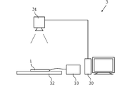
- FIG. 3 is a diagram illustrating a hardware configuration of the inspection apparatus 3.
- the inspection device 3 is a device that quantitatively evaluates the degree of occurrence of bright edges in the surface light source device 1 and automatically determines the presence or absence of bright edges that should be excluded as defects.
- the inspection device 3 generally includes an information processing device (computer) 30, an imaging device 31, a stage 32, and a constant current power source 33.
- the information processing apparatus 30 includes a CPU (central processing unit) that is a hardware processor, a memory that is a main memory, a storage device (such as a hard disk and a flash memory) that temporarily stores programs and data, and an input device (such as a mouse, Keyboard, touch panel, and the like), a display device, an interface with the imaging device 31, a network interface, and the like.
- a CPU central processing unit
- the information processing apparatus 30 includes a CPU (central processing unit) that is a hardware processor, a memory that is a main memory, a storage device (such as a hard disk and a flash memory) that temporarily stores programs and data, and an input device (such as a mouse, Keyboard, touch panel, and the like), a display device, an interface with the imaging device 31, a network interface, and the like.
- the imaging device 31 is a device that photographs the surface light source device 1 placed on the stage 32 and outputs a digital image.
- a digital camera having an optical system, an imaging device, an interface with the information processing device 30, and the like can be used.
- a monochrome camera may be used if the surface light source device 1 is a monochromatic light source, and a color camera is preferable if the surface light source device 1 is a light source of multiple colors.
- the stage 32 is a table on which the surface light source device 1 to be inspected is placed.
- the constant current power source 33 is a device that supplies power to the surface light source device 1.
- the imaging device 31 and the stage 32 may be provided in a clean bench.
- the size of the light emitting surface (vertical and horizontal dimensions) and light emission luminance may be different. Therefore, by adjusting the distance between the stage 32 and the imaging device 31 or the zoom of the imaging device 31 according to the size of the light emitting surface to be inspected, light emission from one pixel of the image obtained by the imaging device 31 is performed. It is also preferable to calibrate the correspondence with the actual size on the surface. It is also preferable to calibrate the average luminance of the image obtained by the imaging device 31 by adjusting the exposure time of the imaging device 31 according to the emission luminance of the inspection target. These calibrations may be automatically executed by the information processing apparatus 30 or manually performed by an operator.
- FIG. 4 is a block diagram showing functions related to the bright edge inspection process of the inspection apparatus 3.
- the inspection device 3 includes an image acquisition unit 40, an inspection unit 41, an output unit 42, and a storage unit 43.
- the image acquisition unit 40 has a function of acquiring image data obtained by photographing the surface light source device 1 to be inspected from the imaging device 31.
- the inspection unit 41 has a function of inspecting the presence or absence of a bright edge by analyzing the image data acquired by the image acquisition unit 40.
- the output unit 42 has a function of outputting information such as image data and inspection results to the display device.
- the storage unit 43 is a function that stores setting data such as a threshold value used for inspection processing. Details of these functions will be described later.
- the function shown in FIG. 4 is basically realized by loading a program required by the CPU of the information processing device 30 from the storage device and executing it. However, some or all of these functions may be replaced with a circuit such as an ASIC or FPGA. Also, by using cloud computing or distributed computing technology, some or all of these functions may be executed by another computer.
- FIG. 5 is a flowchart of the bright edge inspection process in the inspection apparatus 3.
- the inspector arranges the surface light source device 1 at a predetermined position on the stage 32 and the light emitting surface facing the imaging device 31 side. And the surface light source device 1 is connected to the constant current power supply 33, the light source 11 is driven, and the surface light source device 1 is made into a lighting state.
- the inspection object is manually set, but introduction, positioning, connection to and discharge from the power supply, and the like may be automated.
- step S50 the imaging device 31 captures the surface light source device 1 in the lighting state, and the image acquisition unit 40 captures the image data from the imaging device 31.
- the resolution of the image is arbitrary, but in the present embodiment, an image having a resolution of about 0.1 mm (actual size on the light emitting surface) for one pixel is used.
- step S51 the image acquisition unit 40 extracts only the area of the light emitting surface from the input image captured in step S50.
- the image of the light emitting surface area extracted here is hereinafter referred to as a light emitting surface image.
- 6A is an example of the input image 60
- FIG. 6B is an example of the light emitting surface image 61 extracted from the input image 60.
- the light emitting surface image 61 is generated so that the long side of the light emitting surface is parallel to the X axis of the image.
- the image acquisition unit 40 (1) binarizes the original image, (2) removes noise in the background region (region other than the light emitting surface) by closing processing, and (3) extracts the contour of the light emitting surface. May be. Further, when the contour of the light emitting surface is tilted with respect to the image coordinate system, tilt correction (rotation correction) may be performed. Alternatively, when the positioning accuracy on the stage to be inspected is sufficiently high, only a predetermined range in the original image may be cut out.
- the inspection unit 41 inspects the light emitting surface image 61.
- the bright edge that appears along the side parallel to the Y direction of the light emitting surface image as shown in FIG. 6B is the inspection target (that is, the X direction corresponds to the “first direction” of the present invention, The Y direction corresponds to the “second direction” of the present invention).
- the inspection unit 41 sets an inspection range (also referred to as a window) for the light emitting surface image 61.
- the inspection range is a local region used for defect detection and evaluation calculation, and is set to a position where the defect in the light emitting surface image 61 may appear.
- the inspection range 62 may be set along the right end of the light emitting surface image 61.
- a rectangular inspection range 62 having a width in the X direction: 100 pixels (corresponding to about 10 mm) and a width in the Y direction: 200 pixels (corresponding to about 20 mm) will be described.
- the size and shape of the inspection range 62 are arbitrary, and may be appropriately designed according to the size of the light emitting surface to be inspected, the bright edge appearance range, and the like.
- the inspection unit 41 In step S53, the inspection unit 41 generates a one-dimensional luminance profile indicating a change in the luminance value in the X direction in the inspection range 62 based on the image in the inspection range 62. For example, the inspection unit 41 calculates the average of the luminance values (pixel values) for each column of the image within the inspection range 62 (the column indicates 200 pixels arranged in the Y direction), and calculates one-dimensional luminance data (for 100 columns). (Brightness average value data).
- FIG. 7A shows an example of an image in the inspection range 62
- FIG. 7B shows an example of one-dimensional luminance data. The horizontal axis of the graph in FIG.
- the inspection unit 41 performs smoothing processing on the one-dimensional luminance data to reduce noise, and then normalizes the reference luminance value.
- the reference luminance value is a luminance value (normal luminance value) in an area where there is no bright edge.
- the smallest luminance value in the one-dimensional luminance data is used as the reference luminance value.
- the method of determining the reference luminance value is not limited to this.
- the luminance value at the left end (most light source side) in the one-dimensional luminance data may be selected as the reference luminance value, or the average value or the mode value of the luminance in the whole or central portion of the light emitting surface image is used as the reference luminance value. You may choose Alternatively, a fixed value preset in the storage unit 43 may be used.
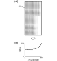
- FIG. 8A is an example of luminance data after normalization. The vertical axis represents the normalized luminance value when the reference luminance value is 1.0. In the present embodiment, the normalized luminance data is referred to as a luminance profile 80.
- the inspection unit 41 detects a bright area from the luminance profile.
- the bright area is an area brighter than the lower limit threshold in the inspection range.
- the lower limit threshold is set to a value 1.025 times the reference luminance value, and an X-direction range in which the luminance value exceeds the lower limit threshold in the luminance profile is detected as a bright region (FIG. 8A).
- the lower threshold value is set because the brightness non-uniformity is not noticeable if the luminance difference from the reference luminance value (that is, the luminance value of the surrounding area) is small (below the lower threshold value). It is because it is not necessary to consider in this.
- step S54 the process proceeds to step S55. If a bright area is not detected, the process proceeds to step S56.
- the inspection unit 41 calculates a bright edge evaluation value from the brightness profile of the bright region. Specifically, as illustrated in FIG. 8B, the inspection unit 41 includes a luminance profile 80 in the bright area, two straight lines 81 and 82 indicating the X-direction range of the bright area, and a straight line 83 indicating the reference luminance value. The area of the closed region (hatched region) 85 surrounded by the straight line 84 indicating the upper threshold is calculated, and this area value is used as the bright edge evaluation value of the inspection range.
- the horizontal width of the closed region 85 corresponds to the size of the bright region
- the vertical width of the closed region 85 corresponds to the luminance of the bright region (luminance difference from the reference luminance value). Therefore, the area value of the closed region 85 corresponds to an evaluation value for evaluating both the size of the bright region and the luminance of the bright region.
- the reason why the upper threshold is set here is as follows. An extremely bright spot may appear locally at the bright edge. In such a case, if the brightness of the spot is used as it is in the calculation of the bright edge evaluation value, the evaluation value becomes excessive and may deviate from the result of the human sensory test. In the human sensory test, if the luminance exceeds a certain level, the evaluation of the luminance unevenness has little effect (that is, if the luminance exceeds a certain level, the human will have the same luminance unevenness regardless of the actual luminance value). It is a tendency to feel.) Therefore, by setting an upper threshold as in this embodiment and reducing the influence of the brightness of the brighter part than the upper threshold on the evaluation value, it is appropriate even when extremely bright spots exist (human sensory test). An evaluation value close to () can be obtained.
- the upper threshold value may be set to an appropriate value based on sensory test results, experimental results, and the like. In the present embodiment, the upper threshold is set to a value 1.15 times the reference luminance value.
- step S56 it is determined whether the inspection unit 41 has obtained evaluation values for all inspection ranges. If there is an unprocessed inspection range, the process returns to step S52, and the inspection range is set to a predetermined pitch (for example, 5 mm) in the Y direction. Shifting and repeating the generation of the brightness profile and the calculation of the bright edge evaluation value (steps S53 to S55). After executing the processing of steps S52 to S55 for all the inspection ranges, the process proceeds to step S57.
- a predetermined pitch for example, 5 mm
- the inspection unit 41 selects the largest one of the bright edge evaluation values of all inspection ranges as a representative evaluation value (step S57), and compares the representative evaluation value with a determination threshold value (step S58).
- the determination threshold value is a threshold value for determining the presence or absence of a bright edge, and may be determined in advance based on the result of sensory inspection or the result of an experiment. If the representative evaluation value is larger than the determination threshold, the inspection unit 41 determines “with bright edge” (step S59), and otherwise determines “without bright edge” (step S60).
- step S61 the output unit 42 generates a screen for outputting information obtained by the inspection unit 41, and outputs the screen to the display device.
- FIG. 9 is an example of an inspection result output screen.
- the input image 90 captured from the imaging device 31, the light-emitting surface image 91 cut out from the input image 90, and the processed image (the light-emitting surface image 91 processed to make the luminance unevenness conspicuous ( 92 (for example, a pseudo color image) is displayed.
- information 93 indicating the position where the bright edge appears (for example, information indicating the inspection range in which the bright edge evaluation value exceeds the determination threshold) 93 is superimposed on the light emitting surface image 91.
- the bright edge evaluation value maximum value (representative evaluation value) 94, the determination result 95, and the luminance profile 96 of the inspection range in which the representative evaluation value is observed are also displayed.
- an evaluation value representing the degree of occurrence of bright edges is calculated based on an image obtained by photographing the light emitting surface of the surface light source device 1, and based on this evaluation value.
- the presence or absence of a bright edge can be determined. Therefore, the bright edge can be inspected objectively and automatically.
- luminance of a bright area is used, the result close
- the inspector can immediately determine the presence / absence of the bright edge and the good / bad of the surface light source device 1. Further, since the bright edge evaluation value is also output, the basis of the determination result can be confirmed, and the satisfaction and objectivity of the determination result are improved.
- the information 93 indicating the position of the bright edge is superimposed on the light emitting surface image 91, it is possible to intuitively and easily grasp the problem portion where the bright edge appears, and for the actual confirmation work. Useful.
- the luminance profile 96 is also displayed, it is possible to grasp the size of the bright region, the luminance difference with respect to the reference luminance, and the like.
- an edge may be an inspection target.
- an inspection range may be set along the upper end and / or lower end of the light emitting surface image, and the bright edge evaluation value may be obtained based on the luminance profile in the Y direction within the inspection range.
- both the bright edge appearing along the side parallel to the Y direction and the bright edge appearing along the side parallel to the X direction may be subject to inspection.
- the bright edge can be inspected by the same method as in the above embodiment.
Abstract
検査装置は、面光源装置の発光面を撮影した画像である発光面画像を取得する画像取得部と、発光面画像内の不具合が現れ得る位置に検査範囲を設定し、検査範囲から下限閾値よりも明るい領域である明領域を検出し、明領域の大きさと明領域の輝度の両方を評価する評価値を計算し、評価値に基づいて不具合の有無を判定する検査部と、検査部により得られた情報を出力する出力部と、を有する。
Description
本発明は、エッジライト型の面光源装置の不具合を検査するための技術に関する。
液晶表示装置のバックライトとして、エッジライト型(Edge-lit)の面光源装置が用いられている。エッジライト型とは、面光源装置の発光面の端縁(エッジ)に沿ってLED(Light Emitting Diode)などの光源を配置し、光源から出射された光を板状のライトガイド(導光板と呼ばれる)により発光面に導く構成である。エッジライト型の面光源装置は、小型化・薄型化が比較的容易であることから、例えばスマートフォンのような小型の電子機器において広く採用されている。
エッジライト型の面光源装置では、導光板の金型や成形の不良、アセンブル時のズレなどの様々な原因により、輝度の不均一に関する不具合が発生することがある。そのような不具合の一つに、光源が配置された部分を除く端部に基準の輝度よりも極端に明るい部分が現れる、というものがある(本明細書ではこの不具合を「ブライトエッジ(Bright edge)」と呼ぶ)。
現状、この種の不具合の検査は、ヒト(検査員)の目視による官能検査に依存しているのが実情である。それゆえ、検査に要する手間及びコスト、属人性の高さなどの課題があり、検査の自動化と客観化(定量化)が求められている。
なお、面光源装置の検査ではないが、特許文献1には、液晶パネルの輝度ムラ(同文献では「シミ欠陥」と称している)を画像処理によって自動で検査する方法が提案されている。しかしながら、本発明者が同文献の方法をブライトエッジの検査に応用できないか試行したが、ヒトの官能検査に近い結果を得ることはできなかった。
本発明は上記実情に鑑みてなされたものであって、エッジライト型の面光源装置において発生する輝度の不均一に関する不具合を客観的かつ自動的に検査するための技術を提供することを目的とする。
上記目的を達成するために、本発明では、ブライトエッジの発生度合いを定量化するための新規の評価値(評価指標)を導入する。そして、本発明は、面光源装置の発光面を撮影した画像から評価値を自動的に計算し、この評価値に基づいてブライトエッジの検査を自動で行うアルゴリズムを提案する。
具体的には、本発明の第一態様は、面光源装置の発光面内の輝度の不均一に関する不具合を検査する検査装置であって、前記面光源装置は、前記発光面の一辺に沿って配置された光源と、前記光源から出射された光を前記発光面に導く導光板と、を有するエッジライト型の面光源装置であり、前記不具合は、前記発光面のうち前記光源が配置された部分を除く端部に、基準輝度よりも明るい部分が現れる不具合であり、
前記検査装置は、前記発光面を撮影した画像である発光面画像を取得する画像取得部と、前記発光面画像内の前記不具合が現れ得る位置に検査範囲を設定し、前記検査範囲から下限閾値よりも明るい領域である明領域を検出し、前記明領域の大きさと前記明領域の輝度の両方を評価する評価値を計算し、前記評価値に基づいて前記不具合の有無を判定する検査部と、前記検査部により得られた情報を出力する出力部と、を有する検査装置を提供する。
前記検査装置は、前記発光面を撮影した画像である発光面画像を取得する画像取得部と、前記発光面画像内の前記不具合が現れ得る位置に検査範囲を設定し、前記検査範囲から下限閾値よりも明るい領域である明領域を検出し、前記明領域の大きさと前記明領域の輝度の両方を評価する評価値を計算し、前記評価値に基づいて前記不具合の有無を判定する検査部と、前記検査部により得られた情報を出力する出力部と、を有する検査装置を提供する。
この構成によれば、面光源装置の発光面を撮影した画像を基に、ブライトエッジの発生度合いを表す評価値を計算し、かつ、この評価値に基づいてブライトエッジの有無を判定することができる。したがって、ブライトエッジを客観的かつ自動的に検査することが可能となる。しかも、本発明は、明領域の大きさと明領域の輝度の両方を評価する評価値を用いるので、従来の官能検査(ヒトの目視検査)に近い結果を得ることができる。
前記検査部は、前記明領域内に上限閾値よりも明るい部分が含まれる場合に、前記評価値の計算において、前記上限閾値よりも明るい部分の輝度を実際よりも小さく評価してもよい。例えば、前記検査部は、前記明領域内に上限閾値よりも明るい部分が含まれる場合に、前記評価値の計算において、前記上限閾値よりも明るい部分の輝度を前記上限閾値と同じ輝度とみなしてもよい。
ブライトエッジでは局所的に極端に明るいスポットが現れる場合がある。このような場合に、そのスポットの輝度をそのまま評価値に反映すると、評価値が過大になってしまい、ヒトの官能検査の結果と乖離する可能性がある。そこで、本発明のように上限閾値を設定し、上限閾値よりも明るい部分の輝度が評価値に与える影響を小さくすることで、極端に明るいスポットが存在する場合でも妥当な(ヒトの官能検査に近い)評価値を得ることができる。
前記発光面画像が第1方向に平行な辺と第2方向に平行な辺を有する矩形の画像であり、前記不具合が第2方向に平行な辺に沿って現れる場合に、前記検査部は、前記検査範囲内における第1方向の輝度値の変化を示す1次元の輝度プロファイルを生成し、前記輝度プロファイルにおいて輝度値が前記下限閾値を超える第1方向の範囲を前記明領域として検出し、前記明領域内の前記輝度プロファイルと、前記明領域の第1方向の範囲を示す2つの直線と、基準輝度を示す直線と、前記上限閾値を示す直線と、で囲まれる閉領域の面積を、前記評価値として計算してもよい。
ここで、「明領域の第1方向の範囲」が明領域の大きさに相当し、「基準輝度を示す直線」と「輝度プロファイル」の間の幅、及び、「基準輝度を示す直線」と「上限閾値を示す直線」の間の幅が明領域の輝度(基準輝度との輝度差)に相当する。したがって、閉領域の面積は、明領域の大きさと明領域の輝度の両方を評価する評価値の一つに該当する。このような閉領域の面積を評価値として用いることにより、簡易な計算で妥当な評価値を得ることができる。
前記基準輝度は、前記検査範囲の前記輝度プロファイルの内で最も小さい輝度値であってもよい。ヒトは局所的な領域内での相対的な輝度の変動を輝度ムラとして感知しやすい。したがって、検査範囲内の最小輝度に基づき基準輝度を設定することで、局所的な(つまり検査範囲内での)輝度ムラの妥当な評価が可能となる。
前記下限閾値及び前記上限閾値は、前記基準輝度に基づいて設定するとよい。例えば、前記下限閾値を前記基準輝度の約1.025倍の値に設定し、前記上限閾値を前記基準輝度の約1.15倍の値に設定すると、ヒトの官能検査に非常に近い評価値を得ることができる。
前記検査範囲の第2方向の幅は、前記発光面画像の第2方向の幅よりも小さいとよい。発光面画像の第2方向の幅の一部分にのみ、ブライトエッジが現れる場合があるからである。
前記出力部は、前記評価値と、前記不具合の有無の判定結果とを出力してもよい。判定結果の出力により、ブライトエッジの有無や面光源装置の良/不良を即座に判断することができる。また、評価値も出力されるので、判定結果の根拠が確認でき、判定結果の納得性・客観性が向上する。
前記出力部は、前記発光面画像又は前記発光面画像を加工した画像の上に、前記不具合が現れている位置を示す情報を重畳した画像を、出力してもよい。このような重畳画像を出力することにより、ブライトエッジが現れている問題箇所を直観的かつ簡易に把握することができ、現物の確認作業にも有用である。
前記出力部は、前記検査範囲の輝度プロファイルを出力してもよい。輝度プロファイルを出力することにより、明領域の大きさや基準輝度に対する輝度差などを把握することができる。
なお、本発明は、上記構成ないし機能の少なくとも一部を有する検査装置又はブライトエッジ定量化装置として捉えることができる。また、本発明は、上記処理の少なくとも一部を含む、検査方法、検査装置の制御方法、ブライトエッジ定量化方法や、これらの方法をコンピュータに実行させるためのプログラム、又は、そのようなプログラムを非一時的に記録したコンピュータ読取可能な記録媒体として捉えることもできる。上記構成及び処理の各々は技術的な矛盾が生じない限り互いに組み合わせて本発明を構成することができる。
本発明によれば、エッジライト型の面光源装置において発生する輝度の不均一に関する不具合を自動的かつ客観的に検査することができる。
本発明は、エッジライト型の面光源装置においてブライトエッジと呼ばれる不具合が発生しているか否かを客観的(定量的)な評価値により評価し、ブライトエッジの有無を自動で検査するための検査技術に関する。この検査技術は、例えば、面光源装置の製造ラインにおける最終工程でのインライン検査や、面光源装置を組み込んだ製品を製造するメーカにおける部品(面光源装置)の受入検査などに好ましく適用できる。なお、以下の実施形態では、液晶表示装置のバックライトとして用いられる面光源装置の例を述べるが、本発明の検査技術は、照明装置やデジタルサイネージなど、他の用途に用いられる面光源装置の検査にも応用することができる。
以下、図面を参照して本発明を実施するための好ましい形態の一例を説明する。ただし、以下の実施形態に記載されている装置の構成や動作は一例であり、本発明の範囲をそれらのみに限定する趣旨のものではない。
(面光源装置)
図1は、面光源装置1の基本的な構成を例示する斜視図である。面光源装置1は、導光板(ライトガイド)10、複数の光源11、フレキシブルプリント基板(以下、「FPC」とも表記する)12、フレーム13、及び固定部材14を備える。また、面光源装置1は、導光板10の下面側に配置される反射シート15を備える。さらに、面光源装置1は、導光板10の上面側に順に積層される拡散シート16、プリズムシート17a、17b、及び遮光シート18を備える。
図1は、面光源装置1の基本的な構成を例示する斜視図である。面光源装置1は、導光板(ライトガイド)10、複数の光源11、フレキシブルプリント基板(以下、「FPC」とも表記する)12、フレーム13、及び固定部材14を備える。また、面光源装置1は、導光板10の下面側に配置される反射シート15を備える。さらに、面光源装置1は、導光板10の上面側に順に積層される拡散シート16、プリズムシート17a、17b、及び遮光シート18を備える。
導光板10は、概略板状で、ポリカーボネート樹脂やポリメチルメタクリレート樹脂等の透光性の素材で成形される。導光板10の上側の面は、光が出射する発光面(光出射面とも称す)となっている。導光板10は、光源11から導光板10内へ導入された光を、全反射を利用して発光面に導き、発光面の全体が略均一に光るようにしたものである。
光源11は、例えば白色光を出射するLED光源である。ただし、白色以外のLED光源やLED光源以外の光源が用いられてもよいし、複数色(例えばRGB)の光源が用いられてもよい。光源11はFPC12に実装されており、FPC12からの給電を受けて駆動される。本実施形態では、導光板10の発光面の一の短辺(「第1の辺」と呼ぶ)に沿って8個の光源11が等間隔に一列に配置されている。
フレーム13は、開口を有し、四辺からなる枠状の部材である。フレーム13は、酸化チタンを含有したポリカーボネート樹脂等により成形される。フレーム13には、導光板10がはめ込まれ、フレーム13の内周面が導光板10の外周面を形成する側面を囲う。フレーム13は、高い反射率を有しており、導光板10内の光が導光板10の外周面から漏れないように光を反射する。フレーム13の一辺には、光源11を収容する収容部が設けられ、収容部には、光源11からの光を反射する反射壁が設けられる。
固定部材14は、FPC12の下面等に配置され、FPC12とフレーム13と導光板10を固定する。固定部材14は、例えば、上下面が粘着面となった両面粘着テープであるが、両面粘着テープに限られるものではない。反射シート15は、反射率の高い白色樹脂シートや金属箔などからなる平滑なシートであり、導光板10内の光が導光板10の下側面から漏れないように光を反射する。拡散シート16は、半透明な樹脂フィルムであり、導光板10の発光面から発せられた光を拡散させて光の指向特性を広げる。プリズムシート17a及び17bは、上面に三角プリズム状の微細なパターンが形成された透明な樹脂フィルムあり、拡散シート16によって拡散された光を集光し、面光源装置1を上面側から見た場合の輝度を上昇させる。遮光シート18は、上下両面が粘着面となった黒色の粘着シートである。遮光シート18は額縁状となっており、光が漏れ出ることを抑制する。
(ブライトエッジ)
図1に例示したエッジライト型の面光源装置では、導光板10の金型や成形の不良、各種部材のアセンブル時のズレ、各種シート15~18の貼り合せ時のズレなどの様々な原因により、輝度の不均一に関する不具合が発生することがある。そのような不具合の一つに、光源11が配置された部分を除く端部に基準輝度よりも極端に明るい部分が現れる「ブライトエッジ」と呼ばれる不具合がある。ブライトエッジは、光源11から導光板10に入射した光が、発光面側に抜けきらず、導光板10の端部まで到達してしまうことが原因で発生するものであり、発生頻度が最も高い不具合の一つである。図2Aのように、光源11が配置された辺(第1の辺)21に対向する辺22に沿ってブライトエッジ20が現れるケースや、図2Bのように、光源11が配置された辺21に直交する辺23,24に沿ってブライトエッジ20が現れるケースもある。なお、導光板が矩形以外の形状(例えば、円形、楕円形、多角形、非対称形状など)を有する場合もあるが、どのような形状の導光板であっても、光源が配置された部分(つまり、光源からの光が入射する部分)を除く端部においてブライトエッジが発生するおそれがある。
図1に例示したエッジライト型の面光源装置では、導光板10の金型や成形の不良、各種部材のアセンブル時のズレ、各種シート15~18の貼り合せ時のズレなどの様々な原因により、輝度の不均一に関する不具合が発生することがある。そのような不具合の一つに、光源11が配置された部分を除く端部に基準輝度よりも極端に明るい部分が現れる「ブライトエッジ」と呼ばれる不具合がある。ブライトエッジは、光源11から導光板10に入射した光が、発光面側に抜けきらず、導光板10の端部まで到達してしまうことが原因で発生するものであり、発生頻度が最も高い不具合の一つである。図2Aのように、光源11が配置された辺(第1の辺)21に対向する辺22に沿ってブライトエッジ20が現れるケースや、図2Bのように、光源11が配置された辺21に直交する辺23,24に沿ってブライトエッジ20が現れるケースもある。なお、導光板が矩形以外の形状(例えば、円形、楕円形、多角形、非対称形状など)を有する場合もあるが、どのような形状の導光板であっても、光源が配置された部分(つまり、光源からの光が入射する部分)を除く端部においてブライトエッジが発生するおそれがある。
本発明者は、ブライトエッジの定量化アルゴリズムの構築と検査の自動化を実現するにあたり、従来の官能検査の手順及び検査結果を分析し、次のような知見を得るに至った。
(1)検査員は、周りに比べて有意に明るい領域(「明領域」と呼ぶ)に注目する。周りに比べてわずかに明るい程度であれば、輝度の不均一は目立たないため問題としない。
(2)検査員は、明領域の面積が広いほど、輝度の不均一が目立つと判断する。
(3)検査員は、明領域とその周りとの輝度差が大きいほど、輝度の不均一が目立つと判断する。ただし、輝度差があるレベルを超えると、検査員が感じる輝度の不均一度合いはほとんど変わらない。
(2)検査員は、明領域の面積が広いほど、輝度の不均一が目立つと判断する。
(3)検査員は、明領域とその周りとの輝度差が大きいほど、輝度の不均一が目立つと判断する。ただし、輝度差があるレベルを超えると、検査員が感じる輝度の不均一度合いはほとんど変わらない。
以上の知見に基づき、本発明者は、明領域の大きさと明領域の輝度の両方を評価する評価値(「ブライトエッジ評価値」と呼ぶ)を設計し、この評価値によりブライトエッジの発生度合いを定量化した。明領域の大きさと明領域の輝度の両方を評価する評価値とは、例えば、評価値が明領域の大きさと明領域の輝度の両方に依存すること、あるいは、評価値が明領域の大きさと明領域の輝度のそれぞれと正の相関をもつことを意味する。このような評価値を導入したことにより、ブライトエッジの発生度合いを定量的かつ客観的に捉えることができるようになり、従来官能検査に頼っていたブライトエッジ検査を自動化できるようになる。以下、本実施形態のブライトエッジ評価値とそれを用いた検査処理の一具体例を詳しく説明する。
(検査装置)
図3を用いて、本発明の実施形態に係る検査装置3の構成を説明する。図3は検査装置3のハードウェア構成を示す図である。この検査装置3は、面光源装置1におけるブライトエッジの発生度合いを定量的に評価し、欠陥として排除すべきブライトエッジの有無を自動で判定する装置である。
図3を用いて、本発明の実施形態に係る検査装置3の構成を説明する。図3は検査装置3のハードウェア構成を示す図である。この検査装置3は、面光源装置1におけるブライトエッジの発生度合いを定量的に評価し、欠陥として排除すべきブライトエッジの有無を自動で判定する装置である。
図3に示すように、検査装置3は、概略、情報処理装置(コンピュータ)30と、撮像装置31と、ステージ32と、定電流電源33とを有している。情報処理装置30は、ハードウェアプロセッサであるCPU(中央演算処理装置)、主記憶であるメモリ、非一時的にプログラムやデータを記憶する記憶装置(ハードディスク、フラッシュメモリなど)、入力装置(マウス、キーボード、タッチパネルなど)、表示装置、撮像装置31とのインタフェース、ネットワークインタフェースなどを有する、汎用又は専用のコンピュータにより構成される。
撮像装置31は、ステージ32上に載置された面光源装置1を撮影し、デジタル画像を出力する装置である。撮像装置31としては、例えば、光学系、撮像素子、情報処理装置30とのインタフェースなどを有するデジタルカメラを用いることができる。面光源装置1の輝度計測が目的のため、面光源装置1が単色光源であればモノクロのカメラでも構わないし、面光源装置1が複数色の光源であればカラーのカメラであることが好ましい。ステージ32は、検査対象となる面光源装置1を載置する台である。定電流電源33は、面光源装置1に電力を供給する装置である。図示しないが、撮像装置31及びステージ32は、クリーンベンチ内に設けられていてもよい。
面光源装置1の型番が異なると、発光面の大きさ(縦横の寸法)や発光輝度が異なる可能性がある。したがって、検査対象の発光面の大きさに応じて、ステージ32と撮像装置31の間の距離、又は、撮像装置31のズームを調整することで、撮像装置31で得られる画像の1画素と発光面上の実寸との対応関係のキャリブレーションを行うことも好ましい。また、検査対象の発光輝度に応じて、撮像装置31の露光時間を調整することで、撮像装置31で得られる画像の平均輝度のキャリブレーションを行うことも好ましい。これらのキャリブレーションは、情報処理装置30が自動で実行してもよいし、作業者が手作業で行ってもよい。
図4は、検査装置3のブライトエッジ検査処理に関わる機能を示すブロック図である。検査装置3は、画像取得部40と、検査部41と、出力部42と、記憶部43とを有する。画像取得部40は、検査対象となる面光源装置1を撮影した画像データを撮像装置31から取得する機能である。検査部41は、画像取得部40により取得された画像データを解析することにより、ブライトエッジの有無を検査する機能である。出力部42は、画像データや検査結果などの情報を表示装置に出力する機能である。記憶部43は、検査処理に用いる閾値などの設定データを記憶している機能である。これらの機能の詳細は後述する。
図4に示す機能は、基本的に、情報処理装置30のCPUが必要なプログラムを記憶装置からロードし、実行することにより実現されるものである。ただし、これらの機能の一部又は全部を、ASICやFPGAなどの回路で代替しても構わない。また、クラウドコンピューティングや分散コンピューティングの技術を利用することで、これらの機能の一部又は全部を他のコンピュータにより実行しても構わない。
(検査処理)
図5を参照して、ブライトエッジ検査処理の流れを説明する。図5は検査装置3におけるブライトエッジ検査処理のフローチャートである。
図5を参照して、ブライトエッジ検査処理の流れを説明する。図5は検査装置3におけるブライトエッジ検査処理のフローチャートである。
まず、検査員が、面光源装置1をステージ32上の所定の位置に、発光面を撮像装置31側に向けて、配置する。そして、面光源装置1を定電流電源33に接続して光源11を駆動し、面光源装置1を点灯状態とする。なお、本実施形態の検査装置3では検査対象の設置を手作業により行うが、検査対象の導入・位置決め・電源との接続・排出などを自動化してもよい。
ステップS50において、撮像装置31が点灯状態の面光源装置1を撮影し、画像取得部40が画像データを撮像装置31から取り込む。画像の解像度は任意であるが、本実施形態では、1画素が約0.1mm(発光面上の実寸)の解像度の画像を用いる。
ステップS51において、画像取得部40が、ステップS50で取り込まれた入力画像から発光面の領域のみを抽出する。ここで抽出された発光面の領域の画像を、以後、発光面画像と呼ぶ。図6Aは入力画像60の一例であり、図6Bは入力画像60から抽出された発光面画像61の一例である。本実施形態では、発光面の長辺が画像のX軸と平行になるように、発光面画像61を生成する。
発光面の領域抽出はどのような方法を用いてもよい。例えば、画像取得部40が、(1)原画像を2値化し、(2)クロージング処理により背景領域(発光面以外の領域)のノイズを除去した後、(3)発光面の輪郭を抽出してもよい。さらに、発光面の輪郭が画像座標系に対して傾いている場合には、傾き補正(回転補正)を行ってもよい。あるいは、検査対象のステージ上の位置決め精度が十分高い場合には、原画像中の所定の範囲を切り出すだけでもよい。
次に、検査部41が発光面画像61の検査を行う。本実施形態では、図6Bのように発光面画像のY方向に平行な辺に沿って現れるブライトエッジを検査の対象とする(つまり、X方向が本発明の「第1方向」に対応し、Y方向が本発明の「第2方向」に対応する。)。
まずステップS52において、検査部41は、発光面画像61に対し検査範囲(ウィンドウとも呼ぶ)を設定する。検査範囲は、不具合の検出及び評価の計算に用いる局所領域であり、発光面画像61内の不具合が現れ得る位置に設定される。図6Bの例では、光源が発光面画像61の左側に配置されているため、発光面画像61の右端に沿って検査範囲62を設定するとよい。以下、一例として、X方向幅:100画素(約10mmに相当)、Y方向幅:200画素(約20mmに相当)の四角形の検査範囲62を用いる例を説明する。ただし、検査範囲62のサイズ及び形状は任意であり、検査対象の発光面の大きさやブライトエッジの出現範囲などに合わせて適宜設計すればよい。
ステップS53において、検査部41は、検査範囲62内の画像に基づいて、検査範囲62内におけるX方向の輝度値の変化を示す1次元の輝度プロファイルを生成する。例えば、検査部41は、検査範囲62内の画像の各列(列はY方向に並ぶ200画素を指す)について輝度値(画素値)の平均を計算し、1次元の輝度データ(100列分の輝度平均値のデータ)を得る。図7Aは検査範囲62内の画像の例、図7Bは1次元の輝度データの例を示す。図7Bのグラフの横軸は検査範囲62内のX方向の画素位置を示し、縦軸は平均輝度値を示している。次に検査部41は、1次元の輝度データに平滑化処理を施してノイズを低減した後、基準輝度値で正規化する。基準輝度値は、ブライトエッジが無い領域の輝度値(通常の輝度値)である。本実施形態では、1次元の輝度データの内で最も小さい輝度値を基準輝度値として用いる。ただし、基準輝度値の決め方はこれに限られない。例えば、1次元の輝度データの内の左端(最も光源側)の輝度値を基準輝度値に選んでもよいし、発光面画像の全体又は中央部分における輝度の平均値や最頻値を基準輝度値に選んでもよい。あるいは、記憶部43に予め設定された固定値を用いてもよい。図8Aは正規化後の輝度データの例である。縦軸は、基準輝度値を1.0としたときの正規化輝度値を示す。本実施形態では、正規化後の輝度データを輝度プロファイル80と呼ぶ。
ステップS54において、検査部41は、輝度プロファイルから明領域を検出する。明領域とは、検査範囲のなかで下限閾値よりも明るい領域である。本実施形態では、下限閾値を基準輝度値の1.025倍の値に設定し、輝度プロファイルにおいて輝度値が下限閾値を超えるX方向範囲を明領域として検出する(図8A)。ここで下限閾値を設けたのは、基準輝度値(すなわち周りの領域の輝度値)との輝度差がわずか(下限閾値以下)であれば、輝度の不均一は目立たないため、ブライトエッジの評価において考慮する必要がないからである。
ステップS54において明領域が検出された場合、ステップS55に進み、明領域が検出されなかった場合は、ステップS56に進む。ステップS55では、検査部41が、明領域の輝度プロファイルからブライトエッジ評価値を計算する。具体的には、図8Bに示すように、検査部41は、明領域内の輝度プロファイル80と、明領域のX方向範囲を示す2つの直線81、82と、基準輝度値を示す直線83と、上限閾値を示す直線84と、で囲まれる閉領域(ハッチングした領域)85の面積を計算し、この面積値を当該検査範囲のブライトエッジ評価値とする。
閉領域85の横幅は明領域の大きさに相当し、閉領域85の縦幅は明領域の輝度(基準輝度値との輝度差)に相当する。したがって、閉領域85の面積値は、明領域の大きさと明領域の輝度の両方を評価する評価値に該当する。
ここで上限閾値を設けたのは次のような理由による。ブライトエッジでは局所的に極端に明るいスポットが現れる場合がある。このような場合に、そのスポットの輝度をそのままブライトエッジ評価値の計算に用いると、評価値が過大になってしまい、ヒトの官能検査の結果と乖離する可能性がある。ヒトの官能検査では、輝度があるレベルを超えると、輝度ムラの評価にはほとんど影響を与えない(つまり、輝度があるレベルを超えると、ヒトは実際の輝度値によらず同程度の輝度ムラと感じる傾向にある。)からである。そこで、本実施形態のように上限閾値を設定し、上限閾値よりも明るい部分の輝度が評価値に与える影響を小さくすることで、極端に明るいスポットが存在する場合でも妥当な(ヒトの官能検査に近い)評価値を得ることができる。上限閾値は官能検査の結果や実験結果などに基づいて適当な値に設定すればよい。本実施形態では、上限閾値を基準輝度値の1.15倍の値に設定する。
ステップS56では、検査部41がすべての検査範囲について評価値を求めたかを判断し、未処理の検査範囲がある場合は、ステップS52に戻り、検査範囲をY方向に所定ピッチ(例えば5mm)だけずらして、輝度プロファイルの生成及びブライトエッジ評価値の計算(ステップS53~S55)を繰り返す。ステップS52~S55の処理をすべての検査範囲について実行した後、ステップS57に進む。
検査部41は、すべての検査範囲のブライトエッジ評価値のなかから最大のものを代表評価値として選択し(ステップS57)、代表評価値を判定閾値と比較する(ステップS58)。判定閾値はブライトエッジの有無を判定するための閾値であり、官能検査の結果や実験結果などに基づいて予め決めておけばよい。検査部41は、代表評価値が判定閾値より大きい場合は「ブライトエッジ有り」と判定し(ステップS59)、そうでない場合は「ブライトエッジ無し」と判定する(ステップS60)。
ステップS61において、出力部42は、検査部41により得られた情報を出力する画面を生成し、表示装置に出力する。図9は検査結果の出力画面の一例である。この出力画面では、撮像装置31から取り込まれた入力画像90と、入力画像90から切り出された発光面画像91と、発光面画像91に対し輝度ムラを目立たせるための加工を施した加工画像(例えば疑似カラー画像など)92が表示されている。また、発光面画像91の上に、ブライトエッジが現れている位置を示す情報(例えば、ブライトエッジ評価値が判定閾値を超えた検査範囲を示す情報)93が重畳表示されている。さらに、ブライトエッジ評価値の最大値(代表評価値)94と判定結果95、及び、その代表評価値が観測された検査範囲の輝度プロファイル96も表示される。
以上述べた本実施形態の検査装置3によれば、面光源装置1の発光面を撮影した画像を基に、ブライトエッジの発生度合いを表す評価値を計算し、かつ、この評価値に基づいてブライトエッジの有無を判定することができる。したがって、ブライトエッジを客観的かつ自動的に検査することが可能となる。しかも、明領域の大きさと明領域の輝度の両方を評価する評価値を用いるので、従来の官能検査(ヒトの目視検査)に近い結果を得ることができる。
また、図9に示す検査結果を出力することにより、検査員は、ブライトエッジの有無や面光源装置1の良/不良を即座に判断することができる。また、ブライトエッジ評価値も出力されるので、判定結果の根拠が確認でき、判定結果の納得性・客観性が向上する。また、発光面画像91の上にブライトエッジの位置を示す情報93が重畳表示されるので、ブライトエッジが現れている問題箇所を直観的かつ簡易に把握することができ、現物の確認作業にも有用である。さらに、輝度プロファイル96も表示されるので、明領域の大きさや基準輝度に対する輝度差などを把握することができる。
(その他)
上記の実施形態の説明は、本発明を例示的に説明するものに過ぎない。本発明は上記の具体的な形態には限定されることはなく、その技術的思想の範囲内で種々の変形が可能である。例えば、上記実施形態では矩形の発光面をもつ面光源装置を例示したが、発光面の形状は矩形に限られない。また、上述したブライトエッジ評価値はあくまで一例であり、明領域の大きさと輝度の両方を評価可能な評価値であればどのように設計してもよい。上述した図5の検査処理では、発光面画像のY方向に平行な辺に沿って現れるブライトエッジのみを検査の対象としたが、図2BのようにX方向に平行な辺に沿って現れるブライトエッジを検査の対象としてもよい。その場合には、例えば、発光面画像の上端及び/又は下端に沿って検査範囲を設定し、検査範囲内におけるY方向の輝度プロファイルを基にブライトエッジ評価値を求めればよい。もちろん、Y方向に平行な辺に沿って現れるブライトエッジとX方向に平行な辺に沿って現れるブライトエッジの両方を検査の対象としてもよい。また、ブライトエッジの現れる辺が、X方向とY方向のいずれとも非平行である場合や、曲線的な辺である場合でも、その辺に沿うように検査範囲を設定するか、あるいは、その辺がX方向又はY方向に平行な直線となるように発光面画像をアフィン変換することにより、上記実施形態と同様の方法でブライトエッジの検査を行うことができる。
上記の実施形態の説明は、本発明を例示的に説明するものに過ぎない。本発明は上記の具体的な形態には限定されることはなく、その技術的思想の範囲内で種々の変形が可能である。例えば、上記実施形態では矩形の発光面をもつ面光源装置を例示したが、発光面の形状は矩形に限られない。また、上述したブライトエッジ評価値はあくまで一例であり、明領域の大きさと輝度の両方を評価可能な評価値であればどのように設計してもよい。上述した図5の検査処理では、発光面画像のY方向に平行な辺に沿って現れるブライトエッジのみを検査の対象としたが、図2BのようにX方向に平行な辺に沿って現れるブライトエッジを検査の対象としてもよい。その場合には、例えば、発光面画像の上端及び/又は下端に沿って検査範囲を設定し、検査範囲内におけるY方向の輝度プロファイルを基にブライトエッジ評価値を求めればよい。もちろん、Y方向に平行な辺に沿って現れるブライトエッジとX方向に平行な辺に沿って現れるブライトエッジの両方を検査の対象としてもよい。また、ブライトエッジの現れる辺が、X方向とY方向のいずれとも非平行である場合や、曲線的な辺である場合でも、その辺に沿うように検査範囲を設定するか、あるいは、その辺がX方向又はY方向に平行な直線となるように発光面画像をアフィン変換することにより、上記実施形態と同様の方法でブライトエッジの検査を行うことができる。
1:面光源装置
10:導光板、11:光源、20:ブライトエッジ
3:検査装置、30:情報処理装置、31:撮像装置、32:ステージ、33:定電流電源
40:画像取得部、41:検査部、42:出力部、43:記憶部
60:入力画像、61:発光面画像
80:輝度プロファイル
10:導光板、11:光源、20:ブライトエッジ
3:検査装置、30:情報処理装置、31:撮像装置、32:ステージ、33:定電流電源
40:画像取得部、41:検査部、42:出力部、43:記憶部
60:入力画像、61:発光面画像
80:輝度プロファイル
Claims (13)
- 面光源装置の発光面内の輝度の不均一に関する不具合を検査する検査装置であって、
前記面光源装置は、前記発光面の一辺に沿って配置された光源と、前記光源から出射された光を前記発光面に導く導光板と、を有するエッジライト型の面光源装置であり、
前記不具合は、前記発光面のうち前記光源が配置された部分を除く端部に、基準輝度よりも明るい部分が現れる不具合であり、
前記検査装置は、
前記発光面を撮影した画像である発光面画像を取得する画像取得部と、
前記発光面画像内の前記不具合が現れ得る位置に検査範囲を設定し、前記検査範囲から下限閾値よりも明るい領域である明領域を検出し、前記明領域の大きさと前記明領域の輝度の両方を評価する評価値を計算し、前記評価値に基づいて前記不具合の有無を判定する検査部と、
前記検査部により得られた情報を出力する出力部と、を有する
ことを特徴とする検査装置。 - 前記検査部は、前記明領域内に上限閾値よりも明るい部分が含まれる場合に、前記評価値の計算において、前記上限閾値よりも明るい部分の輝度を実際よりも小さく評価する
ことを特徴とする請求項1に記載の検査装置。 - 前記検査部は、前記明領域内に上限閾値よりも明るい部分が含まれる場合に、前記評価値の計算において、前記上限閾値よりも明るい部分の輝度を前記上限閾値と同じ輝度とみなす
ことを特徴とする請求項1に記載の検査装置。 - 前記発光面画像が第1方向に平行な辺と第2方向に平行な辺を有する矩形の画像であり、前記不具合が第2方向に平行な辺に沿って現れる場合に、
前記検査部は、
前記検査範囲内における第1方向の輝度値の変化を示す1次元の輝度プロファイルを生成し、前記輝度プロファイルにおいて輝度値が前記下限閾値を超える第1方向の範囲を前記明領域として検出し、
前記明領域内の前記輝度プロファイルと、前記明領域の第1方向の範囲を示す2つの直線と、基準輝度を示す直線と、前記上限閾値を示す直線と、で囲まれる閉領域の面積を、前記評価値として計算する
ことを特徴とする請求項2又は3に記載の検査装置。 - 前記基準輝度は、前記検査範囲の前記輝度プロファイルの内で最も小さい輝度値であることを特徴とする請求項4に記載の検査装置。
- 前記下限閾値は、前記基準輝度の約1.025倍の値に設定される
ことを特徴とする請求項4又は5に記載の検査装置。 - 前記上限閾値は、前記基準輝度の約1.15倍の値に設定される
ことを特徴とする請求項4~6のうちいずれか1項に記載の検査装置。 - 前記検査範囲の第2方向の幅は、前記発光面画像の第2方向の幅よりも小さい
ことを特徴とする請求項4~7のうちいずれか1項に記載の検査装置。 - 前記出力部は、前記評価値と、前記不具合の有無の判定結果とを出力する
ことを特徴とする請求項4~8のうちいずれか1項に記載の検査装置。 - 前記出力部は、前記発光面画像又は前記発光面画像を加工した画像の上に、前記不具合が現れている位置を示す情報を重畳した画像を、出力する
ことを特徴とする請求項4~9のうちいずれか1項に記載の検査装置。 - 前記出力部は、前記検査範囲の輝度プロファイルを出力する
ことを特徴とする請求項4~10のうちいずれか1項に記載の検査装置。 - 面光源装置の発光面内の輝度の不均一に関する不具合を検査する検査方法であって、
前記面光源装置は、前記発光面の一辺に沿って配置された光源と、前記光源から出射された光を前記発光面に導く導光板と、を有するエッジライト型の面光源装置であり、
前記不具合は、前記発光面のうち前記光源が配置された部分を除く端部に、基準輝度よりも明るい部分が現れる不具合であり、
前記検査方法は、
前記発光面を撮影した画像である発光面画像を取得するステップと、
前記発光面画像内の前記不具合が現れ得る位置に検査範囲を設定するステップと、
前記検査範囲から下限閾値よりも明るい領域である明領域を検出するステップと、
前記明領域の大きさと前記明領域の輝度の両方を評価する評価値を計算するステップと、
前記評価値に基づいて前記不具合の有無を判定するステップと、
判定の結果を出力するステップと、を含む
ことを特徴とする検査方法。 - 請求項12に記載の検査方法の各ステップをコンピュータに実行させるためのプログラム。
Priority Applications (4)
| Application Number | Priority Date | Filing Date | Title |
|---|---|---|---|
| EP17881775.5A EP3557217B1 (en) | 2016-12-15 | 2017-10-26 | Inspecting device, inspecting method, and program |
| US16/339,510 US10585045B2 (en) | 2016-12-15 | 2017-10-26 | Inspecting device, inspecting method, and program |
| CN201780060501.0A CN109791089B (zh) | 2016-12-15 | 2017-10-26 | 检查装置、检查方法以及计算机可读取的记录介质 |
| KR1020197008959A KR20190041009A (ko) | 2016-12-15 | 2017-10-26 | 검사 장치, 검사 방법 및 프로그램 |
Applications Claiming Priority (2)
| Application Number | Priority Date | Filing Date | Title |
|---|---|---|---|
| JP2016243248A JP6265254B1 (ja) | 2016-12-15 | 2016-12-15 | 検査装置および検査方法 |
| JP2016-243248 | 2016-12-15 |
Publications (1)
| Publication Number | Publication Date |
|---|---|
| WO2018110112A1 true WO2018110112A1 (ja) | 2018-06-21 |
Family
ID=61020751
Family Applications (1)
| Application Number | Title | Priority Date | Filing Date |
|---|---|---|---|
| PCT/JP2017/038687 WO2018110112A1 (ja) | 2016-12-15 | 2017-10-26 | 検査装置、検査方法、およびプログラム |
Country Status (7)
| Country | Link |
|---|---|
| US (1) | US10585045B2 (ja) |
| EP (1) | EP3557217B1 (ja) |
| JP (1) | JP6265254B1 (ja) |
| KR (1) | KR20190041009A (ja) |
| CN (1) | CN109791089B (ja) |
| TW (1) | TWI639977B (ja) |
| WO (1) | WO2018110112A1 (ja) |
Families Citing this family (4)
| Publication number | Priority date | Publication date | Assignee | Title |
|---|---|---|---|---|
| US11132787B2 (en) * | 2018-07-09 | 2021-09-28 | Instrumental, Inc. | Method for monitoring manufacture of assembly units |
| US20220318667A1 (en) * | 2021-03-30 | 2022-10-06 | Accenture Global Solutions Limited | Intelligent real-time defect prediction, detection, and ai driven automated correction solution |
| CN113252557B (zh) * | 2021-04-08 | 2023-02-03 | 成都小淞科技有限公司 | 条纹结构光喷涂瑕疵检出光源装置 |
| JP2022187661A (ja) * | 2021-06-08 | 2022-12-20 | 富士フイルムビジネスイノベーション株式会社 | 表面検査装置及びプログラム |
Citations (3)
| Publication number | Priority date | Publication date | Assignee | Title |
|---|---|---|---|---|
| JP2005207808A (ja) * | 2004-01-21 | 2005-08-04 | Nidec Copal Corp | 欠陥検査装置及び欠陥検査方法 |
| US20090015825A1 (en) * | 2007-07-11 | 2009-01-15 | Han Rok Chung | Apparatus and method for inspecting liquid crystal display |
| JP2015042942A (ja) * | 2013-08-26 | 2015-03-05 | シャープ株式会社 | 画像処理装置、欠陥検出装置、画像処理方法、プログラム、及び、記録媒体 |
Family Cites Families (16)
| Publication number | Priority date | Publication date | Assignee | Title |
|---|---|---|---|---|
| TWI226959B (en) | 2003-09-30 | 2005-01-21 | Startech Co Ltd | Plane light-source device for identifying images |
| JP2006300913A (ja) * | 2005-04-20 | 2006-11-02 | Selcon Technologies Inc | 導光板外観検査装置 |
| JP2007172397A (ja) | 2005-12-22 | 2007-07-05 | Seiko Epson Corp | エッジ勾配検出方法、シミ欠陥検出方法、エッジ勾配検出装置、シミ欠陥検出装置 |
| JP2007333449A (ja) * | 2006-06-13 | 2007-12-27 | Heiwa Tokei Mfg Co Ltd | 検査装置 |
| US9651729B2 (en) * | 2010-04-16 | 2017-05-16 | Flex Lighting Ii, Llc | Reflective display comprising a frontlight with extraction features and a light redirecting optical element |
| CN102435618A (zh) | 2010-09-29 | 2012-05-02 | 旭硝子株式会社 | 透明板状体的缺陷检查方法及装置 |
| WO2013016729A1 (en) * | 2011-07-28 | 2013-01-31 | Massachusetts Institute Of Technology | Optical tactile sensor |
| CN102494304B (zh) * | 2011-11-30 | 2014-07-16 | 深圳市百得力电子有限公司 | 一种提高侧发光背光源亮度的系统及方法 |
| CN103925992B (zh) * | 2013-01-16 | 2016-03-16 | 光宝电子(广州)有限公司 | 具有背光的装置的亮度测量方法及系统 |
| CN108594342B (zh) * | 2013-12-19 | 2020-09-25 | 康宁股份有限公司 | 用于显示器应用的织构化表面 |
| JP6318694B2 (ja) * | 2014-02-25 | 2018-05-09 | オムロン株式会社 | 検査装置、検査方法、プログラムおよび記録媒体 |
| JP7026309B2 (ja) * | 2015-01-29 | 2022-02-28 | 株式会社 デクシス | 光学式外観検査装置、及びこれを用いた光学式外観検査システム |
| CN104791671A (zh) * | 2015-05-08 | 2015-07-22 | 京东方科技集团股份有限公司 | 一种背光源、测试系统及其测试方法和显示装置 |
| CN104898312A (zh) * | 2015-06-25 | 2015-09-09 | 京东方科技集团股份有限公司 | 一种背光源检测装置及检测方法 |
| JP6671044B2 (ja) * | 2016-03-10 | 2020-03-25 | パナソニックIpマネジメント株式会社 | 液晶バックライト装置 |
| CN106054309A (zh) | 2016-07-28 | 2016-10-26 | 滁州佳宏光电有限公司 | 一种高光效、亮度均匀的导光板及其制造方法 |
-
2016
- 2016-12-15 JP JP2016243248A patent/JP6265254B1/ja active Active
-
2017
- 2017-10-26 US US16/339,510 patent/US10585045B2/en active Active
- 2017-10-26 KR KR1020197008959A patent/KR20190041009A/ko not_active Application Discontinuation
- 2017-10-26 WO PCT/JP2017/038687 patent/WO2018110112A1/ja unknown
- 2017-10-26 EP EP17881775.5A patent/EP3557217B1/en active Active
- 2017-10-26 CN CN201780060501.0A patent/CN109791089B/zh active Active
- 2017-10-31 TW TW106137608A patent/TWI639977B/zh active
Patent Citations (3)
| Publication number | Priority date | Publication date | Assignee | Title |
|---|---|---|---|---|
| JP2005207808A (ja) * | 2004-01-21 | 2005-08-04 | Nidec Copal Corp | 欠陥検査装置及び欠陥検査方法 |
| US20090015825A1 (en) * | 2007-07-11 | 2009-01-15 | Han Rok Chung | Apparatus and method for inspecting liquid crystal display |
| JP2015042942A (ja) * | 2013-08-26 | 2015-03-05 | シャープ株式会社 | 画像処理装置、欠陥検出装置、画像処理方法、プログラム、及び、記録媒体 |
Non-Patent Citations (1)
| Title |
|---|
| See also references of EP3557217A4 * |
Also Published As
| Publication number | Publication date |
|---|---|
| KR20190041009A (ko) | 2019-04-19 |
| TWI639977B (zh) | 2018-11-01 |
| EP3557217B1 (en) | 2022-04-13 |
| CN109791089A (zh) | 2019-05-21 |
| CN109791089B (zh) | 2021-03-05 |
| US20190285554A1 (en) | 2019-09-19 |
| JP6265254B1 (ja) | 2018-01-24 |
| JP2018096904A (ja) | 2018-06-21 |
| EP3557217A4 (en) | 2020-05-20 |
| US10585045B2 (en) | 2020-03-10 |
| TW201824180A (zh) | 2018-07-01 |
| EP3557217A1 (en) | 2019-10-23 |
Similar Documents
| Publication | Publication Date | Title |
|---|---|---|
| JP6265253B1 (ja) | 検査装置および検査方法 | |
| WO2018110112A1 (ja) | 検査装置、検査方法、およびプログラム | |
| US11317067B2 (en) | Method and system for inspecting display image | |
| WO2017202114A1 (zh) | 确定用于检测的光照强度的方法和装置、及光学检测方法和装置 | |
| JP6337949B1 (ja) | スジ状領域検出装置およびスジ状領域検出方法 | |
| JP2000019064A (ja) | フィルム評価方法およびフィルム評価装置 | |
| TWI776275B (zh) | 影像辨識裝置以及影像辨識方法 | |
| JP2009204473A (ja) | 塗装状態検査装置および検査方法 | |
| JP2023121518A (ja) | 外観検査装置、外観検査装置の制御方法、および外観検査装置の制御プログラム | |
| JP4608399B2 (ja) | 照明用光学素子の検査装置 | |
| JP2001153752A (ja) | 拡散板の品質評価方法 | |
| JP2018013455A (ja) | モアレ評価装置およびモアレ評価方法 | |
| JP2004219702A (ja) | 液晶表示装置の検査装置 |
Legal Events
| Date | Code | Title | Description |
|---|---|---|---|
| 121 | Ep: the epo has been informed by wipo that ep was designated in this application |
Ref document number: 17881775 Country of ref document: EP Kind code of ref document: A1 |
|
| ENP | Entry into the national phase |
Ref document number: 20197008959 Country of ref document: KR Kind code of ref document: A |
|
| NENP | Non-entry into the national phase |
Ref country code: DE |
|
| ENP | Entry into the national phase |
Ref document number: 2017881775 Country of ref document: EP Effective date: 20190715 |