WO2018110112A1 - Dispositif d'inspection, procédé d'inspection et programme - Google Patents
Dispositif d'inspection, procédé d'inspection et programme Download PDFInfo
- Publication number
- WO2018110112A1 WO2018110112A1 PCT/JP2017/038687 JP2017038687W WO2018110112A1 WO 2018110112 A1 WO2018110112 A1 WO 2018110112A1 JP 2017038687 W JP2017038687 W JP 2017038687W WO 2018110112 A1 WO2018110112 A1 WO 2018110112A1
- Authority
- WO
- WIPO (PCT)
- Prior art keywords
- inspection
- luminance
- light emitting
- emitting surface
- light source
- Prior art date
Links
- 238000007689 inspection Methods 0.000 title claims abstract description 140
- 238000000034 method Methods 0.000 title claims description 32
- 238000011156 evaluation Methods 0.000 claims abstract description 68
- 230000007547 defect Effects 0.000 claims abstract description 35
- 238000012545 processing Methods 0.000 claims description 9
- 238000004364 calculation method Methods 0.000 claims description 8
- 230000008859 change Effects 0.000 claims description 3
- 238000003384 imaging method Methods 0.000 description 17
- 230000008569 process Effects 0.000 description 14
- 230000001953 sensory effect Effects 0.000 description 14
- 238000010586 diagram Methods 0.000 description 12
- 238000012360 testing method Methods 0.000 description 12
- 230000006870 function Effects 0.000 description 11
- 230000010365 information processing Effects 0.000 description 6
- 238000011002 quantification Methods 0.000 description 4
- 239000011347 resin Substances 0.000 description 4
- 229920005989 resin Polymers 0.000 description 4
- 238000009792 diffusion process Methods 0.000 description 3
- 239000004973 liquid crystal related substance Substances 0.000 description 3
- 230000002093 peripheral effect Effects 0.000 description 3
- 239000000853 adhesive Substances 0.000 description 2
- 230000001070 adhesive effect Effects 0.000 description 2
- 239000002390 adhesive tape Substances 0.000 description 2
- 239000003086 colorant Substances 0.000 description 2
- 238000012790 confirmation Methods 0.000 description 2
- 238000012937 correction Methods 0.000 description 2
- 238000005516 engineering process Methods 0.000 description 2
- 239000000284 extract Substances 0.000 description 2
- 238000000465 moulding Methods 0.000 description 2
- 229920005668 polycarbonate resin Polymers 0.000 description 2
- 239000004431 polycarbonate resin Substances 0.000 description 2
- 238000011179 visual inspection Methods 0.000 description 2
- PXFBZOLANLWPMH-UHFFFAOYSA-N 16-Epiaffinine Natural products C1C(C2=CC=CC=C2N2)=C2C(=O)CC2C(=CC)CN(C)C1C2CO PXFBZOLANLWPMH-UHFFFAOYSA-N 0.000 description 1
- 241000282412 Homo Species 0.000 description 1
- 239000004820 Pressure-sensitive adhesive Substances 0.000 description 1
- GWEVSGVZZGPLCZ-UHFFFAOYSA-N Titan oxide Chemical compound O=[Ti]=O GWEVSGVZZGPLCZ-UHFFFAOYSA-N 0.000 description 1
- 230000001419 dependent effect Effects 0.000 description 1
- 238000013461 design Methods 0.000 description 1
- 238000001514 detection method Methods 0.000 description 1
- 230000000694 effects Effects 0.000 description 1
- 238000002474 experimental method Methods 0.000 description 1
- 239000011888 foil Substances 0.000 description 1
- 238000009499 grossing Methods 0.000 description 1
- 230000003760 hair shine Effects 0.000 description 1
- 238000005286 illumination Methods 0.000 description 1
- 238000004519 manufacturing process Methods 0.000 description 1
- 239000000463 material Substances 0.000 description 1
- 229910052751 metal Inorganic materials 0.000 description 1
- 239000002184 metal Substances 0.000 description 1
- 238000012986 modification Methods 0.000 description 1
- 230000004048 modification Effects 0.000 description 1
- 238000010606 normalization Methods 0.000 description 1
- 230000003287 optical effect Effects 0.000 description 1
- 229920003229 poly(methyl methacrylate) Polymers 0.000 description 1
- 239000004926 polymethyl methacrylate Substances 0.000 description 1
- OGIDPMRJRNCKJF-UHFFFAOYSA-N titanium oxide Inorganic materials [Ti]=O OGIDPMRJRNCKJF-UHFFFAOYSA-N 0.000 description 1
- 230000009466 transformation Effects 0.000 description 1
- 230000000007 visual effect Effects 0.000 description 1
Images


Classifications
-
- G—PHYSICS
- G06—COMPUTING; CALCULATING OR COUNTING
- G06T—IMAGE DATA PROCESSING OR GENERATION, IN GENERAL
- G06T7/00—Image analysis
- G06T7/0002—Inspection of images, e.g. flaw detection
- G06T7/0004—Industrial image inspection
-
- G—PHYSICS
- G01—MEASURING; TESTING
- G01N—INVESTIGATING OR ANALYSING MATERIALS BY DETERMINING THEIR CHEMICAL OR PHYSICAL PROPERTIES
- G01N21/00—Investigating or analysing materials by the use of optical means, i.e. using sub-millimetre waves, infrared, visible or ultraviolet light
- G01N21/84—Systems specially adapted for particular applications
- G01N21/88—Investigating the presence of flaws or contamination
- G01N21/8851—Scan or image signal processing specially adapted therefor, e.g. for scan signal adjustment, for detecting different kinds of defects, for compensating for structures, markings, edges
-
- F—MECHANICAL ENGINEERING; LIGHTING; HEATING; WEAPONS; BLASTING
- F21—LIGHTING
- F21S—NON-PORTABLE LIGHTING DEVICES; SYSTEMS THEREOF; VEHICLE LIGHTING DEVICES SPECIALLY ADAPTED FOR VEHICLE EXTERIORS
- F21S2/00—Systems of lighting devices, not provided for in main groups F21S4/00 - F21S10/00 or F21S19/00, e.g. of modular construction
-
- G—PHYSICS
- G01—MEASURING; TESTING
- G01J—MEASUREMENT OF INTENSITY, VELOCITY, SPECTRAL CONTENT, POLARISATION, PHASE OR PULSE CHARACTERISTICS OF INFRARED, VISIBLE OR ULTRAVIOLET LIGHT; COLORIMETRY; RADIATION PYROMETRY
- G01J1/00—Photometry, e.g. photographic exposure meter
- G01J1/42—Photometry, e.g. photographic exposure meter using electric radiation detectors
- G01J1/44—Electric circuits
-
- G—PHYSICS
- G01—MEASURING; TESTING
- G01M—TESTING STATIC OR DYNAMIC BALANCE OF MACHINES OR STRUCTURES; TESTING OF STRUCTURES OR APPARATUS, NOT OTHERWISE PROVIDED FOR
- G01M11/00—Testing of optical apparatus; Testing structures by optical methods not otherwise provided for
-
- G—PHYSICS
- G02—OPTICS
- G02B—OPTICAL ELEMENTS, SYSTEMS OR APPARATUS
- G02B6/00—Light guides; Structural details of arrangements comprising light guides and other optical elements, e.g. couplings
- G02B6/0001—Light guides; Structural details of arrangements comprising light guides and other optical elements, e.g. couplings specially adapted for lighting devices or systems
- G02B6/0011—Light guides; Structural details of arrangements comprising light guides and other optical elements, e.g. couplings specially adapted for lighting devices or systems the light guides being planar or of plate-like form
-
- G—PHYSICS
- G02—OPTICS
- G02F—OPTICAL DEVICES OR ARRANGEMENTS FOR THE CONTROL OF LIGHT BY MODIFICATION OF THE OPTICAL PROPERTIES OF THE MEDIA OF THE ELEMENTS INVOLVED THEREIN; NON-LINEAR OPTICS; FREQUENCY-CHANGING OF LIGHT; OPTICAL LOGIC ELEMENTS; OPTICAL ANALOGUE/DIGITAL CONVERTERS
- G02F1/00—Devices or arrangements for the control of the intensity, colour, phase, polarisation or direction of light arriving from an independent light source, e.g. switching, gating or modulating; Non-linear optics
- G02F1/01—Devices or arrangements for the control of the intensity, colour, phase, polarisation or direction of light arriving from an independent light source, e.g. switching, gating or modulating; Non-linear optics for the control of the intensity, phase, polarisation or colour
- G02F1/13—Devices or arrangements for the control of the intensity, colour, phase, polarisation or direction of light arriving from an independent light source, e.g. switching, gating or modulating; Non-linear optics for the control of the intensity, phase, polarisation or colour based on liquid crystals, e.g. single liquid crystal display cells
- G02F1/1306—Details
- G02F1/1309—Repairing; Testing
-
- G—PHYSICS
- G02—OPTICS
- G02F—OPTICAL DEVICES OR ARRANGEMENTS FOR THE CONTROL OF LIGHT BY MODIFICATION OF THE OPTICAL PROPERTIES OF THE MEDIA OF THE ELEMENTS INVOLVED THEREIN; NON-LINEAR OPTICS; FREQUENCY-CHANGING OF LIGHT; OPTICAL LOGIC ELEMENTS; OPTICAL ANALOGUE/DIGITAL CONVERTERS
- G02F1/00—Devices or arrangements for the control of the intensity, colour, phase, polarisation or direction of light arriving from an independent light source, e.g. switching, gating or modulating; Non-linear optics
- G02F1/01—Devices or arrangements for the control of the intensity, colour, phase, polarisation or direction of light arriving from an independent light source, e.g. switching, gating or modulating; Non-linear optics for the control of the intensity, phase, polarisation or colour
- G02F1/13—Devices or arrangements for the control of the intensity, colour, phase, polarisation or direction of light arriving from an independent light source, e.g. switching, gating or modulating; Non-linear optics for the control of the intensity, phase, polarisation or colour based on liquid crystals, e.g. single liquid crystal display cells
- G02F1/133—Constructional arrangements; Operation of liquid crystal cells; Circuit arrangements
- G02F1/1333—Constructional arrangements; Manufacturing methods
- G02F1/1335—Structural association of cells with optical devices, e.g. polarisers or reflectors
- G02F1/1336—Illuminating devices
- G02F1/133615—Edge-illuminating devices, i.e. illuminating from the side
-
- G—PHYSICS
- G06—COMPUTING; CALCULATING OR COUNTING
- G06T—IMAGE DATA PROCESSING OR GENERATION, IN GENERAL
- G06T1/00—General purpose image data processing
-
- G—PHYSICS
- G06—COMPUTING; CALCULATING OR COUNTING
- G06T—IMAGE DATA PROCESSING OR GENERATION, IN GENERAL
- G06T7/00—Image analysis
- G06T7/0002—Inspection of images, e.g. flaw detection
- G06T7/0004—Industrial image inspection
- G06T7/0008—Industrial image inspection checking presence/absence
-
- G—PHYSICS
- G02—OPTICS
- G02B—OPTICAL ELEMENTS, SYSTEMS OR APPARATUS
- G02B6/00—Light guides; Structural details of arrangements comprising light guides and other optical elements, e.g. couplings
- G02B6/0001—Light guides; Structural details of arrangements comprising light guides and other optical elements, e.g. couplings specially adapted for lighting devices or systems
- G02B6/0011—Light guides; Structural details of arrangements comprising light guides and other optical elements, e.g. couplings specially adapted for lighting devices or systems the light guides being planar or of plate-like form
- G02B6/0065—Manufacturing aspects; Material aspects
-
- G—PHYSICS
- G02—OPTICS
- G02F—OPTICAL DEVICES OR ARRANGEMENTS FOR THE CONTROL OF LIGHT BY MODIFICATION OF THE OPTICAL PROPERTIES OF THE MEDIA OF THE ELEMENTS INVOLVED THEREIN; NON-LINEAR OPTICS; FREQUENCY-CHANGING OF LIGHT; OPTICAL LOGIC ELEMENTS; OPTICAL ANALOGUE/DIGITAL CONVERTERS
- G02F1/00—Devices or arrangements for the control of the intensity, colour, phase, polarisation or direction of light arriving from an independent light source, e.g. switching, gating or modulating; Non-linear optics
- G02F1/01—Devices or arrangements for the control of the intensity, colour, phase, polarisation or direction of light arriving from an independent light source, e.g. switching, gating or modulating; Non-linear optics for the control of the intensity, phase, polarisation or colour
- G02F1/13—Devices or arrangements for the control of the intensity, colour, phase, polarisation or direction of light arriving from an independent light source, e.g. switching, gating or modulating; Non-linear optics for the control of the intensity, phase, polarisation or colour based on liquid crystals, e.g. single liquid crystal display cells
- G02F1/1303—Apparatus specially adapted to the manufacture of LCDs
-
- G—PHYSICS
- G06—COMPUTING; CALCULATING OR COUNTING
- G06T—IMAGE DATA PROCESSING OR GENERATION, IN GENERAL
- G06T2207/00—Indexing scheme for image analysis or image enhancement
- G06T2207/30—Subject of image; Context of image processing
- G06T2207/30108—Industrial image inspection
-
- G—PHYSICS
- G06—COMPUTING; CALCULATING OR COUNTING
- G06T—IMAGE DATA PROCESSING OR GENERATION, IN GENERAL
- G06T2207/00—Indexing scheme for image analysis or image enhancement
- G06T2207/30—Subject of image; Context of image processing
- G06T2207/30108—Industrial image inspection
- G06T2207/30121—CRT, LCD or plasma display
Definitions
- the present invention relates to a technique for inspecting a defect of an edge light type surface light source device.
- An edge-lit type surface light source device is used as a backlight of a liquid crystal display device.
- the edge light type is a light source such as LED (Light Emitting Diode) arranged along the edge of the light emitting surface of the surface light source device, and the light emitted from the light source is a plate-shaped light guide (with a light guide plate). This is a structure that leads to the light emitting surface.
- the edge light type surface light source device is widely used in small electronic devices such as smartphones because it is relatively easy to reduce the size and thickness.
- a defect related to uneven brightness may occur due to various causes such as a mold of a light guide plate, a molding defect, and a deviation during assembly.
- One such defect is that a portion that is extremely brighter than the standard brightness appears at the end except the portion where the light source is arranged (this specification is referred to as “Bright edge”). ) ").
- Patent Document 1 proposes a method of automatically inspecting luminance unevenness (referred to as “spot defect” in the same document) of a liquid crystal panel by image processing.
- spot defect a method of automatically inspecting luminance unevenness (referred to as “spot defect” in the same document) of a liquid crystal panel by image processing.
- the present inventor tried to apply the method of the same literature to the bright edge inspection, but could not obtain a result close to human sensory inspection.
- the present invention has been made in view of the above circumstances, and an object of the present invention is to provide a technique for objectively and automatically inspecting a defect related to luminance non-uniformity occurring in an edge light type surface light source device. To do.
- the present invention introduces a new evaluation value (evaluation index) for quantifying the degree of occurrence of bright edges.
- the present invention proposes an algorithm for automatically calculating an evaluation value from an image obtained by photographing a light emitting surface of a surface light source device and automatically inspecting a bright edge based on the evaluation value.
- a first aspect of the present invention is an inspection device that inspects a defect related to luminance non-uniformity in a light emitting surface of a surface light source device, wherein the surface light source device is along one side of the light emitting surface.
- An edge light type surface light source device having an arranged light source and a light guide plate that guides light emitted from the light source to the light emitting surface, and the inconvenience is that the light source is arranged in the light emitting surface. It is a problem that a brighter part than the reference brightness appears at the edges excluding the part.
- the inspection apparatus sets an inspection range at a position where the defect can appear in the light emitting surface image, and obtains a light emitting surface image that is an image obtained by photographing the light emitting surface.
- An inspection unit that detects a bright region that is a brighter region, calculates an evaluation value that evaluates both the size of the bright region and the brightness of the bright region, and determines the presence or absence of the defect based on the evaluation value; And an output unit that outputs information obtained by the inspection unit.
- the present invention uses evaluation values that evaluate both the size of the bright area and the brightness of the bright area, it is possible to obtain a result close to the conventional sensory test (human visual inspection).
- the inspection unit may evaluate the luminance of the portion brighter than the upper threshold value in the calculation of the evaluation value smaller than the actual luminance when the bright region includes a portion brighter than the upper threshold value. For example, when the bright area includes a portion brighter than the upper threshold, the inspection unit regards the luminance of the portion brighter than the upper threshold as the same luminance as the upper threshold in the evaluation value calculation. Also good.
- Exceptionally bright spots may appear locally at the bright edge. In such a case, if the brightness of the spot is reflected in the evaluation value as it is, the evaluation value becomes excessive and may deviate from the result of the human sensory test. Therefore, by setting an upper threshold as in the present invention and reducing the influence of the luminance of the brighter part than the upper threshold on the evaluation value, it is appropriate even when extremely bright spots exist (for human sensory tests). A close evaluation value can be obtained.
- the inspection unit When the light emitting surface image is a rectangular image having a side parallel to the first direction and a side parallel to the second direction, and the defect appears along a side parallel to the second direction, the inspection unit, Generating a one-dimensional luminance profile indicating a change in luminance value in the first direction within the inspection range, detecting a range in the first direction in which the luminance value exceeds the lower limit threshold in the luminance profile as the bright region; The area of the closed region surrounded by the luminance profile in the bright region, the two straight lines indicating the range in the first direction of the bright region, the straight line indicating the reference luminance, and the straight line indicating the upper limit threshold value, It may be calculated as an evaluation value.
- the range in the first direction of the bright region corresponds to the size of the bright region, the width between the “straight line indicating the reference luminance” and the “luminance profile”, and the “straight line indicating the reference luminance”
- the width between the “straight line indicating the upper threshold” corresponds to the brightness of the bright area (the brightness difference from the reference brightness). Therefore, the area of the closed region corresponds to one of evaluation values for evaluating both the size of the bright region and the luminance of the bright region. By using the area of such a closed region as an evaluation value, a reasonable evaluation value can be obtained with a simple calculation.
- the reference luminance may be the smallest luminance value in the luminance profile in the inspection range. Humans easily perceive relative luminance fluctuations within a local area as luminance unevenness. Therefore, by setting the reference luminance based on the minimum luminance within the inspection range, it is possible to appropriately evaluate local (that is, within the inspection range) luminance unevenness.
- the lower limit threshold and the upper limit threshold may be set based on the reference luminance. For example, when the lower limit threshold is set to a value about 1.025 times the reference luminance and the upper limit threshold is set to a value about 1.15 times the reference luminance, an evaluation value very close to human sensory test Can be obtained.
- the width of the inspection range in the second direction may be smaller than the width of the light emitting surface image in the second direction. This is because a bright edge may appear only in a part of the width of the light emitting surface image in the second direction.
- the output unit may output the evaluation value and a determination result of the presence or absence of the defect. Based on the output of the determination result, it is possible to immediately determine whether there is a bright edge and whether the surface light source device is good or bad. In addition, since the evaluation value is also output, the basis of the determination result can be confirmed, and the satisfaction and objectivity of the determination result are improved.
- the output unit may output an image in which information indicating a position where the defect appears is superimposed on the light emitting surface image or an image obtained by processing the light emitting surface image.
- the output unit may output a luminance profile of the inspection range. By outputting the luminance profile, it is possible to grasp the size of the bright region, the luminance difference with respect to the reference luminance, and the like.
- the present invention can be understood as an inspection apparatus or a bright edge quantification apparatus having at least a part of the above configuration or function.
- the present invention also includes an inspection method, an inspection apparatus control method, a bright edge quantification method, a program for causing a computer to execute these methods, or such a program, including at least a part of the above processing. It can also be understood as a non-temporarily recorded computer-readable recording medium.
- the present invention it is possible to automatically and objectively inspect defects relating to luminance non-uniformity occurring in an edge light type surface light source device.
- FIG. 1 is a perspective view illustrating a basic configuration of a surface light source device.
- 2A and 2B are diagrams illustrating an example of a bright edge.
- FIG. 3 is a diagram illustrating a hardware configuration of the inspection apparatus.
- FIG. 4 is a block diagram showing functions related to the bright edge inspection process of the inspection apparatus.
- FIG. 5 is a flowchart of the bright edge inspection process in the inspection apparatus.
- FIG. 6A is a diagram illustrating an example of an input image
- FIG. 6B is a diagram illustrating an example of a light emitting surface image extracted from the input image.
- FIG. 7A is a diagram illustrating an example of an image within the inspection range
- FIG. 7B is a diagram illustrating an example of one-dimensional luminance data.
- FIG. 8A is a diagram showing an example of normalized luminance data (luminance profile), and
- FIG. 8B is a diagram for explaining bright edge evaluation values.
- FIG. 9 is a diagram showing an example of an inspection
- the present invention evaluates whether or not a defect called a bright edge has occurred in an edge light type surface light source device using an objective (quantitative) evaluation value, and an inspection for automatically inspecting the presence or absence of a bright edge Regarding technology.
- This inspection technique can be preferably applied to, for example, in-line inspection at the final process in a surface light source device production line, or acceptance inspection of a part (surface light source device) in a manufacturer that manufactures a product incorporating the surface light source device.
- an example of a surface light source device used as a backlight of a liquid crystal display device will be described.
- the inspection technique of the present invention is a surface light source device used for other applications such as an illumination device and digital signage. It can also be applied to inspection.
- FIG. 1 is a perspective view illustrating the basic configuration of the surface light source device 1.
- the surface light source device 1 includes a light guide plate (light guide) 10, a plurality of light sources 11, a flexible printed circuit board (hereinafter also referred to as “FPC”) 12, a frame 13, and a fixing member 14. Further, the surface light source device 1 includes a reflection sheet 15 disposed on the lower surface side of the light guide plate 10. Furthermore, the surface light source device 1 includes a diffusion sheet 16, prism sheets 17 a and 17 b, and a light shielding sheet 18 that are sequentially stacked on the upper surface side of the light guide plate 10.
- FPC flexible printed circuit board
- the light guide plate 10 has a substantially plate shape and is formed of a light-transmitting material such as polycarbonate resin or polymethyl methacrylate resin.
- the upper surface of the light guide plate 10 is a light emitting surface from which light is emitted (also referred to as a light emitting surface).
- the light guide plate 10 guides light introduced from the light source 11 into the light guide plate 10 to the light emitting surface using total reflection so that the entire light emitting surface shines substantially uniformly.
- the light source 11 is, for example, an LED light source that emits white light. However, LED light sources other than white and light sources other than LED light sources may be used, and light sources of multiple colors (for example, RGB) may be used.
- the light source 11 is mounted on the FPC 12 and is driven by receiving power from the FPC 12. In the present embodiment, eight light sources 11 are arranged in a line at equal intervals along one short side (referred to as “first side”) of the light emitting surface of the light guide plate 10.
- the frame 13 is a frame-shaped member having an opening and having four sides.
- the frame 13 is molded from a polycarbonate resin containing titanium oxide or the like.
- the light guide plate 10 is fitted into the frame 13, and the inner peripheral surface of the frame 13 surrounds the side surface forming the outer peripheral surface of the light guide plate 10.
- the frame 13 has a high reflectance, and reflects light so that light in the light guide plate 10 does not leak from the outer peripheral surface of the light guide plate 10.
- a housing part that houses the light source 11 is provided on one side of the frame 13, and a reflecting wall that reflects light from the light source 11 is provided in the housing part.
- the fixing member 14 is disposed on the lower surface of the FPC 12 and fixes the FPC 12, the frame 13, and the light guide plate 10.
- the fixing member 14 is, for example, a double-sided adhesive tape whose upper and lower surfaces are adhesive surfaces, but is not limited to a double-sided adhesive tape.
- the reflection sheet 15 is a smooth sheet made of a highly reflective white resin sheet, metal foil, or the like, and reflects light so that light in the light guide plate 10 does not leak from the lower surface of the light guide plate 10.
- the diffusion sheet 16 is a translucent resin film, and diffuses the light emitted from the light emitting surface of the light guide plate 10 to widen the directional characteristics of the light.
- the prism sheets 17a and 17b are transparent resin films having a triangular prism-like fine pattern formed on the upper surface, condensing the light diffused by the diffusion sheet 16, and viewing the surface light source device 1 from the upper surface side. Increase the brightness.
- the light shielding sheet 18 is a black pressure-sensitive adhesive sheet whose upper and lower surfaces are adhesive surfaces. The light shielding sheet 18 has a frame shape and suppresses light from leaking out.
- the light guide plate may have a shape other than a rectangle (for example, a circle, an ellipse, a polygon, an asymmetric shape, etc.). That is, there is a possibility that a bright edge occurs at an end portion excluding a portion where light from the light source is incident.
- the present inventor analyzed the procedure and test results of conventional sensory tests and realized the following knowledge in order to construct a bright edge quantification algorithm and automate the test.
- the inspector pays attention to an area significantly brighter than the surrounding area (referred to as “bright area”). As long as it is slightly brighter than the surroundings, uneven brightness is not noticeable and does not matter. (2) The inspector determines that the uneven brightness is more conspicuous as the area of the bright region is larger. (3) The inspector determines that the uneven brightness is more conspicuous as the brightness difference between the bright area and the surrounding area is larger. However, when the luminance difference exceeds a certain level, the degree of non-uniformity in luminance felt by the inspector hardly changes.
- the present inventor designed an evaluation value (referred to as “bright edge evaluation value”) for evaluating both the size of the bright area and the luminance of the bright area, and the degree of occurrence of the bright edge based on this evaluation value.
- the evaluation value for evaluating both the size of the bright region and the luminance of the bright region is, for example, that the evaluation value depends on both the size of the bright region and the luminance of the bright region, or the evaluation value is the same as the size of the bright region. This means that there is a positive correlation with each of the brightness in the bright area.
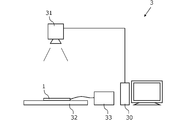
- FIG. 3 is a diagram illustrating a hardware configuration of the inspection apparatus 3.
- the inspection device 3 is a device that quantitatively evaluates the degree of occurrence of bright edges in the surface light source device 1 and automatically determines the presence or absence of bright edges that should be excluded as defects.
- the inspection device 3 generally includes an information processing device (computer) 30, an imaging device 31, a stage 32, and a constant current power source 33.
- the information processing apparatus 30 includes a CPU (central processing unit) that is a hardware processor, a memory that is a main memory, a storage device (such as a hard disk and a flash memory) that temporarily stores programs and data, and an input device (such as a mouse, Keyboard, touch panel, and the like), a display device, an interface with the imaging device 31, a network interface, and the like.
- a CPU central processing unit
- the information processing apparatus 30 includes a CPU (central processing unit) that is a hardware processor, a memory that is a main memory, a storage device (such as a hard disk and a flash memory) that temporarily stores programs and data, and an input device (such as a mouse, Keyboard, touch panel, and the like), a display device, an interface with the imaging device 31, a network interface, and the like.
- the imaging device 31 is a device that photographs the surface light source device 1 placed on the stage 32 and outputs a digital image.
- a digital camera having an optical system, an imaging device, an interface with the information processing device 30, and the like can be used.
- a monochrome camera may be used if the surface light source device 1 is a monochromatic light source, and a color camera is preferable if the surface light source device 1 is a light source of multiple colors.
- the stage 32 is a table on which the surface light source device 1 to be inspected is placed.
- the constant current power source 33 is a device that supplies power to the surface light source device 1.
- the imaging device 31 and the stage 32 may be provided in a clean bench.
- the size of the light emitting surface (vertical and horizontal dimensions) and light emission luminance may be different. Therefore, by adjusting the distance between the stage 32 and the imaging device 31 or the zoom of the imaging device 31 according to the size of the light emitting surface to be inspected, light emission from one pixel of the image obtained by the imaging device 31 is performed. It is also preferable to calibrate the correspondence with the actual size on the surface. It is also preferable to calibrate the average luminance of the image obtained by the imaging device 31 by adjusting the exposure time of the imaging device 31 according to the emission luminance of the inspection target. These calibrations may be automatically executed by the information processing apparatus 30 or manually performed by an operator.
- FIG. 4 is a block diagram showing functions related to the bright edge inspection process of the inspection apparatus 3.
- the inspection device 3 includes an image acquisition unit 40, an inspection unit 41, an output unit 42, and a storage unit 43.
- the image acquisition unit 40 has a function of acquiring image data obtained by photographing the surface light source device 1 to be inspected from the imaging device 31.
- the inspection unit 41 has a function of inspecting the presence or absence of a bright edge by analyzing the image data acquired by the image acquisition unit 40.
- the output unit 42 has a function of outputting information such as image data and inspection results to the display device.
- the storage unit 43 is a function that stores setting data such as a threshold value used for inspection processing. Details of these functions will be described later.
- the function shown in FIG. 4 is basically realized by loading a program required by the CPU of the information processing device 30 from the storage device and executing it. However, some or all of these functions may be replaced with a circuit such as an ASIC or FPGA. Also, by using cloud computing or distributed computing technology, some or all of these functions may be executed by another computer.
- FIG. 5 is a flowchart of the bright edge inspection process in the inspection apparatus 3.
- the inspector arranges the surface light source device 1 at a predetermined position on the stage 32 and the light emitting surface facing the imaging device 31 side. And the surface light source device 1 is connected to the constant current power supply 33, the light source 11 is driven, and the surface light source device 1 is made into a lighting state.
- the inspection object is manually set, but introduction, positioning, connection to and discharge from the power supply, and the like may be automated.
- step S50 the imaging device 31 captures the surface light source device 1 in the lighting state, and the image acquisition unit 40 captures the image data from the imaging device 31.
- the resolution of the image is arbitrary, but in the present embodiment, an image having a resolution of about 0.1 mm (actual size on the light emitting surface) for one pixel is used.
- step S51 the image acquisition unit 40 extracts only the area of the light emitting surface from the input image captured in step S50.
- the image of the light emitting surface area extracted here is hereinafter referred to as a light emitting surface image.
- 6A is an example of the input image 60
- FIG. 6B is an example of the light emitting surface image 61 extracted from the input image 60.
- the light emitting surface image 61 is generated so that the long side of the light emitting surface is parallel to the X axis of the image.
- the image acquisition unit 40 (1) binarizes the original image, (2) removes noise in the background region (region other than the light emitting surface) by closing processing, and (3) extracts the contour of the light emitting surface. May be. Further, when the contour of the light emitting surface is tilted with respect to the image coordinate system, tilt correction (rotation correction) may be performed. Alternatively, when the positioning accuracy on the stage to be inspected is sufficiently high, only a predetermined range in the original image may be cut out.
- the inspection unit 41 inspects the light emitting surface image 61.
- the bright edge that appears along the side parallel to the Y direction of the light emitting surface image as shown in FIG. 6B is the inspection target (that is, the X direction corresponds to the “first direction” of the present invention, The Y direction corresponds to the “second direction” of the present invention).
- the inspection unit 41 sets an inspection range (also referred to as a window) for the light emitting surface image 61.
- the inspection range is a local region used for defect detection and evaluation calculation, and is set to a position where the defect in the light emitting surface image 61 may appear.
- the inspection range 62 may be set along the right end of the light emitting surface image 61.
- a rectangular inspection range 62 having a width in the X direction: 100 pixels (corresponding to about 10 mm) and a width in the Y direction: 200 pixels (corresponding to about 20 mm) will be described.
- the size and shape of the inspection range 62 are arbitrary, and may be appropriately designed according to the size of the light emitting surface to be inspected, the bright edge appearance range, and the like.
- the inspection unit 41 In step S53, the inspection unit 41 generates a one-dimensional luminance profile indicating a change in the luminance value in the X direction in the inspection range 62 based on the image in the inspection range 62. For example, the inspection unit 41 calculates the average of the luminance values (pixel values) for each column of the image within the inspection range 62 (the column indicates 200 pixels arranged in the Y direction), and calculates one-dimensional luminance data (for 100 columns). (Brightness average value data).
- FIG. 7A shows an example of an image in the inspection range 62
- FIG. 7B shows an example of one-dimensional luminance data. The horizontal axis of the graph in FIG.
- the inspection unit 41 performs smoothing processing on the one-dimensional luminance data to reduce noise, and then normalizes the reference luminance value.
- the reference luminance value is a luminance value (normal luminance value) in an area where there is no bright edge.
- the smallest luminance value in the one-dimensional luminance data is used as the reference luminance value.
- the method of determining the reference luminance value is not limited to this.
- the luminance value at the left end (most light source side) in the one-dimensional luminance data may be selected as the reference luminance value, or the average value or the mode value of the luminance in the whole or central portion of the light emitting surface image is used as the reference luminance value. You may choose Alternatively, a fixed value preset in the storage unit 43 may be used.
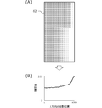
- FIG. 8A is an example of luminance data after normalization. The vertical axis represents the normalized luminance value when the reference luminance value is 1.0. In the present embodiment, the normalized luminance data is referred to as a luminance profile 80.
- the inspection unit 41 detects a bright area from the luminance profile.
- the bright area is an area brighter than the lower limit threshold in the inspection range.
- the lower limit threshold is set to a value 1.025 times the reference luminance value, and an X-direction range in which the luminance value exceeds the lower limit threshold in the luminance profile is detected as a bright region (FIG. 8A).
- the lower threshold value is set because the brightness non-uniformity is not noticeable if the luminance difference from the reference luminance value (that is, the luminance value of the surrounding area) is small (below the lower threshold value). It is because it is not necessary to consider in this.
- step S54 the process proceeds to step S55. If a bright area is not detected, the process proceeds to step S56.
- the inspection unit 41 calculates a bright edge evaluation value from the brightness profile of the bright region. Specifically, as illustrated in FIG. 8B, the inspection unit 41 includes a luminance profile 80 in the bright area, two straight lines 81 and 82 indicating the X-direction range of the bright area, and a straight line 83 indicating the reference luminance value. The area of the closed region (hatched region) 85 surrounded by the straight line 84 indicating the upper threshold is calculated, and this area value is used as the bright edge evaluation value of the inspection range.
- the horizontal width of the closed region 85 corresponds to the size of the bright region
- the vertical width of the closed region 85 corresponds to the luminance of the bright region (luminance difference from the reference luminance value). Therefore, the area value of the closed region 85 corresponds to an evaluation value for evaluating both the size of the bright region and the luminance of the bright region.
- the reason why the upper threshold is set here is as follows. An extremely bright spot may appear locally at the bright edge. In such a case, if the brightness of the spot is used as it is in the calculation of the bright edge evaluation value, the evaluation value becomes excessive and may deviate from the result of the human sensory test. In the human sensory test, if the luminance exceeds a certain level, the evaluation of the luminance unevenness has little effect (that is, if the luminance exceeds a certain level, the human will have the same luminance unevenness regardless of the actual luminance value). It is a tendency to feel.) Therefore, by setting an upper threshold as in this embodiment and reducing the influence of the brightness of the brighter part than the upper threshold on the evaluation value, it is appropriate even when extremely bright spots exist (human sensory test). An evaluation value close to () can be obtained.
- the upper threshold value may be set to an appropriate value based on sensory test results, experimental results, and the like. In the present embodiment, the upper threshold is set to a value 1.15 times the reference luminance value.
- step S56 it is determined whether the inspection unit 41 has obtained evaluation values for all inspection ranges. If there is an unprocessed inspection range, the process returns to step S52, and the inspection range is set to a predetermined pitch (for example, 5 mm) in the Y direction. Shifting and repeating the generation of the brightness profile and the calculation of the bright edge evaluation value (steps S53 to S55). After executing the processing of steps S52 to S55 for all the inspection ranges, the process proceeds to step S57.
- a predetermined pitch for example, 5 mm
- the inspection unit 41 selects the largest one of the bright edge evaluation values of all inspection ranges as a representative evaluation value (step S57), and compares the representative evaluation value with a determination threshold value (step S58).
- the determination threshold value is a threshold value for determining the presence or absence of a bright edge, and may be determined in advance based on the result of sensory inspection or the result of an experiment. If the representative evaluation value is larger than the determination threshold, the inspection unit 41 determines “with bright edge” (step S59), and otherwise determines “without bright edge” (step S60).
- step S61 the output unit 42 generates a screen for outputting information obtained by the inspection unit 41, and outputs the screen to the display device.
- FIG. 9 is an example of an inspection result output screen.
- the input image 90 captured from the imaging device 31, the light-emitting surface image 91 cut out from the input image 90, and the processed image (the light-emitting surface image 91 processed to make the luminance unevenness conspicuous ( 92 (for example, a pseudo color image) is displayed.
- information 93 indicating the position where the bright edge appears (for example, information indicating the inspection range in which the bright edge evaluation value exceeds the determination threshold) 93 is superimposed on the light emitting surface image 91.
- the bright edge evaluation value maximum value (representative evaluation value) 94, the determination result 95, and the luminance profile 96 of the inspection range in which the representative evaluation value is observed are also displayed.
- an evaluation value representing the degree of occurrence of bright edges is calculated based on an image obtained by photographing the light emitting surface of the surface light source device 1, and based on this evaluation value.
- the presence or absence of a bright edge can be determined. Therefore, the bright edge can be inspected objectively and automatically.
- luminance of a bright area is used, the result close
- the inspector can immediately determine the presence / absence of the bright edge and the good / bad of the surface light source device 1. Further, since the bright edge evaluation value is also output, the basis of the determination result can be confirmed, and the satisfaction and objectivity of the determination result are improved.
- the information 93 indicating the position of the bright edge is superimposed on the light emitting surface image 91, it is possible to intuitively and easily grasp the problem portion where the bright edge appears, and for the actual confirmation work. Useful.
- the luminance profile 96 is also displayed, it is possible to grasp the size of the bright region, the luminance difference with respect to the reference luminance, and the like.
- an edge may be an inspection target.
- an inspection range may be set along the upper end and / or lower end of the light emitting surface image, and the bright edge evaluation value may be obtained based on the luminance profile in the Y direction within the inspection range.
- both the bright edge appearing along the side parallel to the Y direction and the bright edge appearing along the side parallel to the X direction may be subject to inspection.
- the bright edge can be inspected by the same method as in the above embodiment.
Landscapes
- Physics & Mathematics (AREA)
- General Physics & Mathematics (AREA)
- Engineering & Computer Science (AREA)
- Nonlinear Science (AREA)
- Chemical & Material Sciences (AREA)
- Optics & Photonics (AREA)
- Theoretical Computer Science (AREA)
- Crystallography & Structural Chemistry (AREA)
- Analytical Chemistry (AREA)
- Computer Vision & Pattern Recognition (AREA)
- General Engineering & Computer Science (AREA)
- Quality & Reliability (AREA)
- Signal Processing (AREA)
- Spectroscopy & Molecular Physics (AREA)
- Life Sciences & Earth Sciences (AREA)
- Biochemistry (AREA)
- General Health & Medical Sciences (AREA)
- Immunology (AREA)
- Pathology (AREA)
- Health & Medical Sciences (AREA)
- Mathematical Physics (AREA)
- Investigating Materials By The Use Of Optical Means Adapted For Particular Applications (AREA)
- Liquid Crystal (AREA)
- Image Analysis (AREA)
- Testing Of Optical Devices Or Fibers (AREA)
- Planar Illumination Modules (AREA)
- Image Processing (AREA)
Abstract
La présente invention concerne un dispositif d'inspection qui comprend : une unité d'acquisition d'image destinée à acquérir une image de surface d'émission de lumière qui est une image obtenue par capture d'une surface d'émission de lumière d'un dispositif de source de lumière de surface; une unité d'inspection destinée à régler une plage d'inspection dans une position dans laquelle peuvent apparaître des défauts dans l'image de surface d'émission de lumière, à détecter, à partir de la plage d'inspection, une région lumineuse qui est une région plus lumineuse qu'un seuil limite inférieur, à calculer une valeur d'évaluation pour évaluer à la fois la taille de la région lumineuse et la luminosité de la région lumineuse et à déterminer la présence/l'absence d'un défaut sur la base de la valeur d'évaluation; et une unité de sortie destinée à délivrer des informations acquises par l'unité d'inspection.
Priority Applications (4)
| Application Number | Priority Date | Filing Date | Title |
|---|---|---|---|
| CN201780060501.0A CN109791089B (zh) | 2016-12-15 | 2017-10-26 | 检查装置、检查方法以及计算机可读取的记录介质 |
| KR1020197008959A KR20190041009A (ko) | 2016-12-15 | 2017-10-26 | 검사 장치, 검사 방법 및 프로그램 |
| US16/339,510 US10585045B2 (en) | 2016-12-15 | 2017-10-26 | Inspecting device, inspecting method, and program |
| EP17881775.5A EP3557217B1 (fr) | 2016-12-15 | 2017-10-26 | Dispositif d'inspection, procédé d'inspection et programme |
Applications Claiming Priority (2)
| Application Number | Priority Date | Filing Date | Title |
|---|---|---|---|
| JP2016243248A JP6265254B1 (ja) | 2016-12-15 | 2016-12-15 | 検査装置および検査方法 |
| JP2016-243248 | 2016-12-15 |
Publications (1)
| Publication Number | Publication Date |
|---|---|
| WO2018110112A1 true WO2018110112A1 (fr) | 2018-06-21 |
Family
ID=61020751
Family Applications (1)
| Application Number | Title | Priority Date | Filing Date |
|---|---|---|---|
| PCT/JP2017/038687 WO2018110112A1 (fr) | 2016-12-15 | 2017-10-26 | Dispositif d'inspection, procédé d'inspection et programme |
Country Status (7)
| Country | Link |
|---|---|
| US (1) | US10585045B2 (fr) |
| EP (1) | EP3557217B1 (fr) |
| JP (1) | JP6265254B1 (fr) |
| KR (1) | KR20190041009A (fr) |
| CN (1) | CN109791089B (fr) |
| TW (1) | TWI639977B (fr) |
| WO (1) | WO2018110112A1 (fr) |
Families Citing this family (5)
| Publication number | Priority date | Publication date | Assignee | Title |
|---|---|---|---|---|
| US11132787B2 (en) * | 2018-07-09 | 2021-09-28 | Instrumental, Inc. | Method for monitoring manufacture of assembly units |
| US20220318667A1 (en) * | 2021-03-30 | 2022-10-06 | Accenture Global Solutions Limited | Intelligent real-time defect prediction, detection, and ai driven automated correction solution |
| CN113252557B (zh) * | 2021-04-08 | 2023-02-03 | 成都小淞科技有限公司 | 条纹结构光喷涂瑕疵检出光源装置 |
| JP2022187661A (ja) * | 2021-06-08 | 2022-12-20 | 富士フイルムビジネスイノベーション株式会社 | 表面検査装置及びプログラム |
| CN117889751A (zh) * | 2024-03-18 | 2024-04-16 | 珠海新立电子科技有限公司 | 一种fpc的贴片精度检测方法及系统 |
Citations (3)
| Publication number | Priority date | Publication date | Assignee | Title |
|---|---|---|---|---|
| JP2005207808A (ja) * | 2004-01-21 | 2005-08-04 | Nidec Copal Corp | 欠陥検査装置及び欠陥検査方法 |
| US20090015825A1 (en) * | 2007-07-11 | 2009-01-15 | Han Rok Chung | Apparatus and method for inspecting liquid crystal display |
| JP2015042942A (ja) * | 2013-08-26 | 2015-03-05 | シャープ株式会社 | 画像処理装置、欠陥検出装置、画像処理方法、プログラム、及び、記録媒体 |
Family Cites Families (16)
| Publication number | Priority date | Publication date | Assignee | Title |
|---|---|---|---|---|
| TWI226959B (en) | 2003-09-30 | 2005-01-21 | Startech Co Ltd | Plane light-source device for identifying images |
| JP2006300913A (ja) * | 2005-04-20 | 2006-11-02 | Selcon Technologies Inc | 導光板外観検査装置 |
| JP2007172397A (ja) * | 2005-12-22 | 2007-07-05 | Seiko Epson Corp | エッジ勾配検出方法、シミ欠陥検出方法、エッジ勾配検出装置、シミ欠陥検出装置 |
| JP2007333449A (ja) * | 2006-06-13 | 2007-12-27 | Heiwa Tokei Mfg Co Ltd | 検査装置 |
| US9651729B2 (en) * | 2010-04-16 | 2017-05-16 | Flex Lighting Ii, Llc | Reflective display comprising a frontlight with extraction features and a light redirecting optical element |
| CN102435618A (zh) | 2010-09-29 | 2012-05-02 | 旭硝子株式会社 | 透明板状体的缺陷检查方法及装置 |
| US9127938B2 (en) * | 2011-07-28 | 2015-09-08 | Massachusetts Institute Of Technology | High-resolution surface measurement systems and methods |
| CN102494304B (zh) * | 2011-11-30 | 2014-07-16 | 深圳市百得力电子有限公司 | 一种提高侧发光背光源亮度的系统及方法 |
| CN103925992B (zh) * | 2013-01-16 | 2016-03-16 | 光宝电子(广州)有限公司 | 具有背光的装置的亮度测量方法及系统 |
| KR102396551B1 (ko) * | 2013-12-19 | 2022-05-12 | 코닝 인코포레이티드 | 디스플레이 응용을 위한 텍스쳐링된 표면 |
| JP6318694B2 (ja) * | 2014-02-25 | 2018-05-09 | オムロン株式会社 | 検査装置、検査方法、プログラムおよび記録媒体 |
| KR20170107952A (ko) * | 2015-01-29 | 2017-09-26 | 가부시키가이샤 데크시스 | 광학식 외관 검사 장치 및 이를 이용한 광학식 외관 검사 시스템 |
| CN104791671A (zh) * | 2015-05-08 | 2015-07-22 | 京东方科技集团股份有限公司 | 一种背光源、测试系统及其测试方法和显示装置 |
| CN104898312A (zh) * | 2015-06-25 | 2015-09-09 | 京东方科技集团股份有限公司 | 一种背光源检测装置及检测方法 |
| JP6671044B2 (ja) * | 2016-03-10 | 2020-03-25 | パナソニックIpマネジメント株式会社 | 液晶バックライト装置 |
| CN106054309A (zh) | 2016-07-28 | 2016-10-26 | 滁州佳宏光电有限公司 | 一种高光效、亮度均匀的导光板及其制造方法 |
-
2016
- 2016-12-15 JP JP2016243248A patent/JP6265254B1/ja active Active
-
2017
- 2017-10-26 WO PCT/JP2017/038687 patent/WO2018110112A1/fr unknown
- 2017-10-26 EP EP17881775.5A patent/EP3557217B1/fr active Active
- 2017-10-26 US US16/339,510 patent/US10585045B2/en active Active
- 2017-10-26 CN CN201780060501.0A patent/CN109791089B/zh active Active
- 2017-10-26 KR KR1020197008959A patent/KR20190041009A/ko not_active Application Discontinuation
- 2017-10-31 TW TW106137608A patent/TWI639977B/zh active
Patent Citations (3)
| Publication number | Priority date | Publication date | Assignee | Title |
|---|---|---|---|---|
| JP2005207808A (ja) * | 2004-01-21 | 2005-08-04 | Nidec Copal Corp | 欠陥検査装置及び欠陥検査方法 |
| US20090015825A1 (en) * | 2007-07-11 | 2009-01-15 | Han Rok Chung | Apparatus and method for inspecting liquid crystal display |
| JP2015042942A (ja) * | 2013-08-26 | 2015-03-05 | シャープ株式会社 | 画像処理装置、欠陥検出装置、画像処理方法、プログラム、及び、記録媒体 |
Non-Patent Citations (1)
| Title |
|---|
| See also references of EP3557217A4 * |
Also Published As
| Publication number | Publication date |
|---|---|
| EP3557217B1 (fr) | 2022-04-13 |
| CN109791089A (zh) | 2019-05-21 |
| TW201824180A (zh) | 2018-07-01 |
| JP2018096904A (ja) | 2018-06-21 |
| US10585045B2 (en) | 2020-03-10 |
| EP3557217A4 (fr) | 2020-05-20 |
| EP3557217A1 (fr) | 2019-10-23 |
| KR20190041009A (ko) | 2019-04-19 |
| JP6265254B1 (ja) | 2018-01-24 |
| US20190285554A1 (en) | 2019-09-19 |
| CN109791089B (zh) | 2021-03-05 |
| TWI639977B (zh) | 2018-11-01 |
Similar Documents
| Publication | Publication Date | Title |
|---|---|---|
| WO2018110112A1 (fr) | Dispositif d'inspection, procédé d'inspection et programme | |
| JP6265253B1 (ja) | 検査装置および検査方法 | |
| US11317067B2 (en) | Method and system for inspecting display image | |
| WO2017202114A1 (fr) | Procédé et appareil de détermination d'intensité d'éclairage pour une inspection, et procédé et appareil d'inspection optique | |
| JP6337949B1 (ja) | スジ状領域検出装置およびスジ状領域検出方法 | |
| JP2000019064A (ja) | フィルム評価方法およびフィルム評価装置 | |
| TWI776275B (zh) | 影像辨識裝置以及影像辨識方法 | |
| JP2009204473A (ja) | 塗装状態検査装置および検査方法 | |
| JP4608399B2 (ja) | 照明用光学素子の検査装置 | |
| JP2001153752A (ja) | 拡散板の品質評価方法 | |
| JP2018013455A (ja) | モアレ評価装置およびモアレ評価方法 | |
| JP2004219702A (ja) | 液晶表示装置の検査装置 | |
| JP2010133794A (ja) | 線幅測定方法 |
Legal Events
| Date | Code | Title | Description |
|---|---|---|---|
| 121 | Ep: the epo has been informed by wipo that ep was designated in this application |
Ref document number: 17881775 Country of ref document: EP Kind code of ref document: A1 |
|
| ENP | Entry into the national phase |
Ref document number: 20197008959 Country of ref document: KR Kind code of ref document: A |
|
| NENP | Non-entry into the national phase |
Ref country code: DE |
|
| ENP | Entry into the national phase |
Ref document number: 2017881775 Country of ref document: EP Effective date: 20190715 |