WO2018110071A1 - バスバ構造およびそれを用いた電力変換装置 - Google Patents
バスバ構造およびそれを用いた電力変換装置 Download PDFInfo
- Publication number
- WO2018110071A1 WO2018110071A1 PCT/JP2017/037542 JP2017037542W WO2018110071A1 WO 2018110071 A1 WO2018110071 A1 WO 2018110071A1 JP 2017037542 W JP2017037542 W JP 2017037542W WO 2018110071 A1 WO2018110071 A1 WO 2018110071A1
- Authority
- WO
- WIPO (PCT)
- Prior art keywords
- bus bar
- terminal
- capacitor
- bsb1
- bsb2
- Prior art date
- Legal status (The legal status is an assumption and is not a legal conclusion. Google has not performed a legal analysis and makes no representation as to the accuracy of the status listed.)
- Ceased
Links
Images





Classifications
-
- H—ELECTRICITY
- H02—GENERATION; CONVERSION OR DISTRIBUTION OF ELECTRIC POWER
- H02M—APPARATUS FOR CONVERSION BETWEEN AC AND AC, BETWEEN AC AND DC, OR BETWEEN DC AND DC, AND FOR USE WITH MAINS OR SIMILAR POWER SUPPLY SYSTEMS; CONVERSION OF DC OR AC INPUT POWER INTO SURGE OUTPUT POWER; CONTROL OR REGULATION THEREOF
- H02M7/00—Conversion of AC power input into DC power output; Conversion of DC power input into AC power output
- H02M7/003—Constructional details, e.g. physical layout, assembly, wiring or busbar connections
-
- H—ELECTRICITY
- H02—GENERATION; CONVERSION OR DISTRIBUTION OF ELECTRIC POWER
- H02M—APPARATUS FOR CONVERSION BETWEEN AC AND AC, BETWEEN AC AND DC, OR BETWEEN DC AND DC, AND FOR USE WITH MAINS OR SIMILAR POWER SUPPLY SYSTEMS; CONVERSION OF DC OR AC INPUT POWER INTO SURGE OUTPUT POWER; CONTROL OR REGULATION THEREOF
- H02M1/00—Details of apparatus for conversion
- H02M1/44—Circuits or arrangements for compensating for electromagnetic interference in converters or inverters
-
- H—ELECTRICITY
- H02—GENERATION; CONVERSION OR DISTRIBUTION OF ELECTRIC POWER
- H02M—APPARATUS FOR CONVERSION BETWEEN AC AND AC, BETWEEN AC AND DC, OR BETWEEN DC AND DC, AND FOR USE WITH MAINS OR SIMILAR POWER SUPPLY SYSTEMS; CONVERSION OF DC OR AC INPUT POWER INTO SURGE OUTPUT POWER; CONTROL OR REGULATION THEREOF
- H02M7/00—Conversion of AC power input into DC power output; Conversion of DC power input into AC power output
- H02M7/42—Conversion of DC power input into AC power output without possibility of reversal
- H02M7/44—Conversion of DC power input into AC power output without possibility of reversal by static converters
- H02M7/48—Conversion of DC power input into AC power output without possibility of reversal by static converters using discharge tubes with control electrode or semiconductor devices with control electrode
- H02M7/53—Conversion of DC power input into AC power output without possibility of reversal by static converters using discharge tubes with control electrode or semiconductor devices with control electrode using devices of a triode or transistor type requiring continuous application of a control signal
- H02M7/537—Conversion of DC power input into AC power output without possibility of reversal by static converters using discharge tubes with control electrode or semiconductor devices with control electrode using devices of a triode or transistor type requiring continuous application of a control signal using semiconductor devices only, e.g. single switched pulse inverters
- H02M7/5387—Conversion of DC power input into AC power output without possibility of reversal by static converters using discharge tubes with control electrode or semiconductor devices with control electrode using devices of a triode or transistor type requiring continuous application of a control signal using semiconductor devices only, e.g. single switched pulse inverters in a bridge configuration
Definitions
- the present invention relates to a bus bar structure and a power conversion device using the same, for example, a power conversion device mounted on an electric vehicle and a bus bar structure used therefor.
- a power conversion device mounted on an electric vehicle is connected to a high voltage battery by a cable, converts a DC voltage supplied from the high voltage battery into an AC voltage, supplies power to the electric motor, and rotates the electric motor.
- the power conversion device includes a plurality of switching elements, and converts the DC voltage into an AC voltage by, for example, periodically switching these switching elements.
- the power conversion device includes a bus bar that electrically connects the power input terminal to which the cable is connected and the switching element.
- Patent Document 1 An example of a power converter is described in Patent Document 1.
- the voltage / current in the bus bar fluctuates and electromagnetic noise is generated.
- the generated electromagnetic noise leaks from the casing of the power converter. That is, high voltage conduction noise is generated.
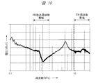
- FIG. 10 is a characteristic diagram showing noise frequency characteristics measured by the present inventors.
- the horizontal axis represents the frequency
- the vertical axis represents the noise peak voltage value at the frequency.
- noise exists in a wide frequency band.
- the frequency bands shown in FIG. 10 for example, 0.52 to 1.73 MHz is an AM broadcast frequency band, and for example 7.1 to 26.1 MHz is a SW (Short Wave) frequency band.
- FIG. 11 is an explanatory diagram for explaining the study of the present inventors.
- FIGS. 11A and 11B are block diagrams for explaining the relationship between the high voltage battery and the power converter, and FIG. 11C shows a change in the current flowing through the voltage wiring.
- HVBT indicates a high voltage battery
- HP indicates an anode terminal of the high voltage battery HVBT
- HN indicates a cathode terminal
- PWCS indicates a power converter
- PP indicates an anode power input terminal (hereinafter also referred to as an input terminal or a first power input terminal) of the power converter PWCS
- PN indicates a cathode power input terminal (input). Terminal or second power input terminal).
- the casings of the high voltage battery HVBT and the power converter PWCS are connected to a ground line GND such as a ground as a frame ground G.
- the anode terminal HP of the high voltage battery HVBT and the input terminal PP of the power converter PWCS are electrically connected by the voltage wiring VLP, and the cathode terminal HN of the high voltage battery HVBT and the input terminal of the power converter PWCS.
- the PN is electrically connected by a voltage wiring VLN.
- the power conversion device PWCS starts the conversion operation, current is supplied from the anode terminal HP of the high voltage battery HVBT to the voltage wiring VLP.
- the current flowing through the anode terminal HP can be regarded as being constituted by a normal mode current NMI and a common mode current CMI.
- the current flowing through the cathode terminal HN of the high voltage battery HVBT can also be regarded as being constituted by the normal mode current NMI and the common mode current CMI.
- the common mode current CMI supplied from the anode terminal HP and the cathode terminal HN to the voltage wirings VLP and VLN passes through the power conversion device PWCS via the input terminals PP and PN, and goes from the frame ground G to the ground line GND.
- the normal mode current NMI is supplied from the anode terminal HP to the voltage wiring VLP and the input terminal PP, and returns from the input terminal PN to the voltage wiring VLN and the anode terminal HN through the power converter PWCS.
- FIG. 11B is a diagram showing a normal mode voltage NMV corresponding to the normal mode current NMI and a common mode voltage CMV corresponding to the common mode current CMI. Since normal mode current NMI is a current that reciprocates between voltage lines VLP and VLN and returns to high voltage battery HVBT, normal mode voltage NMV is a potential difference between voltage lines VLP and VLN. On the other hand, the common mode current CMI is a current that returns from each of the voltage wirings VLP and VLN to the high voltage battery HVBT through the ground line GND. Therefore, the common mode voltage CMV is based on the voltage (ground voltage) of the ground line GND. Resulting in a potential difference.
- the common mode voltage CMV appears as a change in potential difference with respect to the ground voltage (ground line GND), and the normal mode voltage NMV is between the voltage wirings VLP and VLN. It appears as a change in potential difference.
- harmonic components constituting the noise are superimposed on each of the normal mode current NMI and the common mode current CMI, and change according to the noise. Similarly, the normal mode voltage NMV and the common mode voltage CMV are changed by superimposing harmonic components.
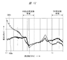
- FIG. 12 is a characteristic diagram showing noise frequency characteristics measured by the present inventors.
- the horizontal axis indicates the frequency
- the vertical axis indicates the noise peak current value at the frequency.
- a broken line CMIn is a characteristic curve indicating common mode current noise
- a solid line NMIn is a characteristic curve indicating normal mode current noise. That is, the characteristic curve CMIn shows a noise component (common mode noise current) in the common mode current CMI superimposed based on the harmonic component of noise
- the characteristic curve NMIn is a normal mode superimposed based on the harmonic component of noise.
- a noise component (normal mode noise current) in the current NMI is shown. 12 corresponds to the noise frequency characteristic shown in FIG. 10 divided into a normal mode noise current and a common mode noise current.
- the normal mode noise current is larger than the common mode noise current in the AM broadcast frequency band and the SW frequency band. Therefore, the present inventors considered that it is important to reduce the normal mode noise current.
- Patent Document 1 describes a power conversion device including a stubber circuit that can be miniaturized. However, Patent Document 1 does not disclose suppression of noise in the AM broadcast frequency band and SW frequency band.
- An object of the present invention is to provide a bus bar structure capable of suppressing noise in the AM broadcast frequency band and the SW frequency band, and a power conversion device having the bus bar structure.
- a power conversion device is connected between an anode terminal and a cathode terminal of a power supply, smoothes noise (voltage change) superimposed on a DC voltage, and converts the DC voltage into an AC voltage.
- a switching circuit that converts the power source, a first bus bar that electrically connects the anode terminal of the power source and the first terminal of the first capacitor unit, and a cathode terminal of the power source and the second terminal of the first capacitor unit.
- a second bus bar electrically connected to each other, and a second capacitor portion electrically connected between the first bus bar and the second bus bar.
- the first bus bar and the second bus bar have portions that face each other (opposing portions), and are arranged so that the directions of currents flowing in the opposing portions that face each other (opposing portions) are the same.
- FIG. 1 is a block diagram illustrating a configuration of a power conversion device according to a first embodiment.
- 1 is a plan view schematically showing the structure of a power converter according to Embodiment 1.
- FIG. (A) to (C) are diagrams showing the structure of the bus bar according to the first embodiment. It is a figure which shows the relationship between the structure of the bus bar concerning Embodiment 1, and an inductance.
- FIG. 6 is a characteristic diagram showing the attenuation amount of the LCL filter according to the first embodiment. 6 is a perspective view showing a structure of a bus bar according to Embodiment 2.
- FIG. (A) to (C) are diagrams showing the structure of a bus bar according to the second embodiment.
- FIG. 1 A) to (C) are diagrams showing the structure of the bus bar according to the third embodiment.
- (A) And (B) is a perspective view which shows the structure of the bus bar concerning Embodiment 4.
- FIG. It is a characteristic view which shows the noise frequency characteristic which the present inventors measured.
- (A)-(C) are explanatory drawings for demonstrating examination of the present inventors. It is a characteristic view which shows the noise frequency characteristic which the present inventors measured. It is a circuit diagram which shows the equivalent circuit of the noise filter which the present inventors considered. It is a characteristic view which shows the attenuation amount of a LCL filter.
- the present inventors considered combining a noise filter with the bus bar in order to reduce normal mode noise current and suppress noise in the AM broadcast frequency band and SW frequency band. That is, the capacitor is coupled to the bus bar that electrically connects the anode power input terminal and the switching element of the power converter and the bus bar that electrically connects the cathode power input terminal and the switching element. I thought.
- the capacitor is configured by a capacitor connected between the bus bars and a capacitor connected between each bus bar and the frame ground. Since the bus bar is made of, for example, a copper plate, it has a parasitic inductor. Therefore, a noise filter is constituted by the capacitor and the bus bar inductor.
- FIG. 13 is a circuit diagram showing an equivalent circuit of a noise filter considered by the present inventors.
- the power source V2 represents an equivalent circuit of the high voltage battery HVBT
- Gn represents an equivalent circuit of a switching element (switching circuit)
- V1 represents a power source formed by conversion by the power conversion circuit PWCS.
- the power source V2 is a high DC voltage
- the power source V1 is an AC voltage formed by switching of the switching element Gn.
- Resistors R4 and R5 indicate impedance matching resistors.
- the switching element Gn is shown as a noise generation source.
- BSB1 indicates a first bus bar that connects between the input terminal PP of the power converter PWCS and the switching element Gn
- BSB2 connects between the input terminal PN of the power converter PWCS and the switching element Gn.
- the 2nd bus bar is shown.
- Cxp represents a smoothing capacitive element (smoothing capacitor) that is connected between the first bus bar BSB1 and the second bus bar BSB2 and smoothes a voltage change superimposed on the DC voltage V2 due to noise.
- Cyp is a capacitive element Cyp1 (not shown) connected between the first bus bar BSB1 and the frame ground G, and a capacitive element Cyp2 (not shown) connected between the second bus bar BSB2 and the frame ground G.
- capacitance part comprised by these is shown.
- the capacitive elements Cyp1 and Cyp2 are equivalently connected in series between the first bus bar BSB1 and the second bus bar BSB2. Therefore, in the equivalent circuit diagram, the capacitive elements Cyp1 and Cyp2 are depicted as a capacitive part Cyp connected between the first bus bar BSB1 and the second bus bar BSB2.
- the capacitor part (filter capacitor part) Cx constituting the noise filter is connected to predetermined positions of the first bus bar BSB1 and the second bus bar BSB2. That is, in the first bus bar BSB1 and the second bus bar BSB2, the capacitor Cx is connected at a position between the input terminals PP and PN and the switching element Gn.
- the first bus bar BSB1 is equivalently composed of two inductors (first inductor portion and second inductor portion) Lp1 and Lp2 with the position where the capacitor portion Cx is connected as a boundary.
- the second bus bar BSB2 is equivalently constituted by two inductors (third inductor portion and fourth inductor portion) Ln1 and Ln2 with the position of the capacitor portion Cx as a boundary.
- the mark * attached to the inductors Lp1, Lp2, Ln1, and Ln2 indicates the direction of magnetic field generation.
- K1 represents a mutual coupling coefficient (hereinafter also simply referred to as a coupling coefficient) between the inductors Lp1 and Ln1
- k2 represents a coupling coefficient between the inductors Lp2 and Ln2.
- the capacitor unit Cx includes capacitive elements C1 to C3 and resistors R1 to R3.
- the capacitive element C1 and the resistor R1 are connected in series between the first bus bar BSB1 and the second bus bar BSB2.
- the capacitive element C2 and the resistor R2 are also connected in series between the first bus bar BSB1 and the second bus bar BSB2.
- the capacitive element C3 has two capacitive elements C31 (not shown) and C32 (not shown), and the resistor R3 also has two resistors R31 (not shown) and R32 (not shown).
- the capacitive element C31 and the resistor R31 are connected in series between the first bus bar BSB1 and the frame ground G, and the capacitive element C32 and the resistor R32 are also connected in series between the second bus bar BSB2 and the frame ground G.
- the capacitive element C31, the resistor R31, the capacitive element C32, and the resistor R32 are equivalently connected in series between the first bus bar BSB1 and the second bus bar BSB2 as in the above-described capacitive unit Cyp. It becomes the composition. Therefore, similarly to the capacitive part Cyp, these capacitive elements C31, C32 and resistors R31, R32 are depicted as a capacitive element C3 and a resistor R3 connected in series between the first bus bar BSB1 and the second bus bar BSB2. Yes.
- the resistors R1 to R3 included in the capacitor unit Cx function as dump resistors that suppress noise peaks.
- a noise filter in which a capacitor Cx is sandwiched between a first inductor unit La configured by inductors Lp1 and Ln1 and a second inductor unit Lb configured by inductors Lp2 and Ln2 is configured.
- a filter arranged so that the capacitor Cx is sandwiched between the two inductors La and Lb is also referred to as an LCL filter.
- the capacitor portion (for convenience, the capacitor portion Cxx) is configured by the capacitor portion Cyp and the smoothing capacitor element Cxp.
- the first filter circuit is configured by the first inductor unit La and the capacitor unit Cx
- the second filter circuit is configured by the second inductor unit Lb and the capacitor unit Cxx.
- the first filter circuit and the second filter circuit are coupled in series in this order between the input terminals PP and PN and the switching element Gn.
- such a filter is also referred to as an LCLC filter.
- the capacitance of the capacitive element constituting the capacitive part Cx is increased.
- the capacitance elements C1 to C3 become large, or each capacitance element is constituted by a plurality of capacitance elements.
- downsizing of the power conversion device PWCS is hindered.
- FIG. 14 is a characteristic diagram showing the attenuation of the LCL (LCLC) filter shown in FIG.
- the horizontal axis represents the frequency F
- the vertical axis represents the ratio of the voltages V1 and V2 shown in FIG. 13 in decibels (dBV).
- a characteristic curve GLb0 represented by an alternate long and short dash line indicates a change in attenuation accompanying a change in the frequency F when the inductances of the inductors Lp2 and Ln2 are set to 0 nH.
- a characteristic curve GLb1 represented by a solid line indicates a change in attenuation when the inductances of the inductors Lp2 and Ln2 are larger than 0 nH, and a two-dot chain line characteristic curve GLb2 indicates an inductance when the characteristic curve GLb1 is measured.
- the change in attenuation when an inductor having an inductance three times as large as that of the inductors Lp2 and Ln2 is shown. Note that the inductance of the inductor unit La and the capacitance of the capacitor unit Cx are the same when the characteristic curves GLb0 to GLB2 are obtained.
- the inductance of the inductor portion Lb constituting the LCL (LCLC) filter when the inductance of the inductor portion Lb constituting the LCL (LCLC) filter is increased, the amount of attenuation can be increased. That is, by increasing the value of the inductor Lb disposed between the capacitor Cx and the capacitor Cyp or / and the smoothing capacitor Cxp among the inductors constituting the LCL (LCLC) filter, it is effective. It is possible to increase the attenuation amount.
- the resonance frequency fp can be obtained by Expression (1).
- CCx represents the capacitance of the capacitive part Cx
- HLb represents the inductance of the inductor part Lb.
- the resonance unit fp and the inductor unit Lb are set so that the resonance frequency fp is smaller than 0.52 MHz which is the lowest frequency of the AM broadcast frequency band. The value of will be set.
- the inductance HLb of the inductor portion Lb can be obtained by Expression (2).
- HLp2 indicates the inductance of the inductor Lp2
- HLn2 indicates the inductance of the inductor Ln2
- k2 is a coupling coefficient of the inductors Lp2 and Ln2.
- the inductance HLb of the inductor Lb is obtained by multiplying the sum of the inductances HLp2 and HLn2 of the two inductors Lp2 and Ln2 by the product of the inductances HLp2 and HLn2. The value obtained by adding or subtracting the mutual inductance value obtained in this way. This addition or subtraction is determined by whether the directions of the magnetic fields generated by the inductors Lp2 and Ln2 are the same or opposite.
- each of the inductors Lp2 and Ln2 is considered to be composed of a plurality of partial inductors.
- the first bus bar BSB1 and the second bus bar BSB2 are arranged so as to generate magnetic fields in the same direction in a part of the plurality of partial inductors. Thereby, the inductance HLb in the inductor portion Lb increases.
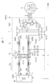
- FIG. 1 is a block diagram illustrating a configuration of the power conversion apparatus according to the first embodiment.
- 1 has shown the housing
- Various circuit blocks and elements are stored in the housing 1 to constitute a power conversion device PWCS.
- FIG. 1 only circuit blocks and elements stored in the housing 1 that are necessary for explanation are illustrated.
- the figure shows a high voltage battery HVBT that supplies a DC voltage to the power converter PWCS and an electric motor 4 that is driven by an AC voltage formed by the power converter PWCS.
- the high voltage battery HVBT includes a battery BT, the anode electrode of the battery BT is connected to the anode terminal HP of the high voltage battery HVBT, and the cathode electrode of the battery BT is connected to the cathode terminal HN of the high voltage battery HVBT.
- the casing of the high-voltage battery HVBT serves as a frame ground G and is connected to the ground line GND.
- Anode terminal HP and cathode terminal HN of high-voltage battery HVBT are electrically connected by cable 2 to input terminal (anode power input terminal) PP and input terminal (cathode power input terminal) PN of power converter PWCS. ing.
- the electric motor 4 is not particularly limited, but is constituted by a three-phase electric motor.
- the electric motor 4 includes a rotor (not shown) and a stator (not shown), and three coils 5-U, 5-V and 5-W are arranged on the stator.
- the power converter PWCS generates a three-phase AC voltage and supplies it to the three coils 5-U, 5-V and 5-W via the cable 3.
- the coils 5-U, 5-V and 5-W generate a magnetic field corresponding to the three-phase AC voltage, and the rotor rotates.
- the housing of the electric motor 4 has a frame ground G and is connected to the ground line GND.
- the power conversion device PWCS includes a switching circuit SWC, a first bus bar BSB1, a second bus bar BSB2, and capacitive elements C1, C2, C31, C32, Cxp, which electrically connect the switching circuit SWC and the input terminals PP, PN. Cyp1, Cyp2 and resistors R1, R2, R31, R32 are provided.
- the switching circuit SWC includes three unit switching circuits USW1 to USW3 having the same configuration.
- the unit switching circuit USW1 will be described as an example.
- the unit switching circuit USW1 includes insulated gate bipolar transistors (hereinafter simply referred to as transistors) TR1 and TR2 and diodes D1 and D2.
- Diodes D1 and D2 are connected between the collectors and emitters of the transistors TR1 and TR2, respectively.
- the emitter of the transistor TR1 is connected to the collector of the transistor TR2.
- a connection node between the emitter and the collector is an output node, and is connected to the coil of the electric motor 4 via the cable 3.
- the collector of the transistor TR1 is electrically connected to the input terminal PP by the first bus bar BSB1, and the emitter of the transistor TR2 is electrically connected to the input terminal PN by the second bus bar BSB2.
- a switch control signal from a switching control circuit (not shown) is supplied to the gates of the transistors TR1 and TR2, and the transistors TR1 and TR2 are controlled to be switched on and off in a complementary manner by the switch control signal.
- the transistors TR1 and TR2 are complementarily turned on / off, an anode voltage and a cathode voltage are periodically output to the output node. That is, an AC voltage is output from the output node. Since the same applies to the remaining unit switching circuits USW2 and USW3, the description thereof is omitted. Since the transistors are periodically turned on / off in this way, the voltage / current in the first bus bar BSB1 and the second bus bar BSB2 changes, and noise is generated.
- Each of the first bus bar BSB1 and the second bus bar BSB2 is not particularly limited, but is a copper plate made of copper, and both ends thereof constitute a pair of terminals.
- One terminal of the first bus bar BSB1 is connected to the input terminal PP of the power converter PWCS, and the other terminal PPO is the first terminal TCx1 of the smoothing capacitive element (first capacitive part) Cxp that functions as a smoothing capacitor.
- the other terminal PPO is connected to the collector of the transistor TR1 in the unit switching circuits USW1 to USW3.
- the second bus bar BSB2 has one terminal connected to the input terminal PN of the power converter PWCS, and the other terminal PNO connected to the second terminal TCx2 of the smoothing capacitive element Cxp, and the capacitance.
- the second terminal TCy12 of the element Cyp1 and the second terminal TCy22 of the capacitive element Cyp2 are connected.
- the other terminal PPO is connected to the emitter of the transistor TR2 in the unit switching circuits USW1 to USW3.
- the other terminals PPO and PNO of the first bus bar BSB1 and the second bus bar BSB2 are drawn separately from the capacitive elements Cxp, Cyp1, Cyp2 and the collectors and emitters of the transistors in order to make the drawing easier to see.
- the present invention is not limited to this.
- the first bus bar BSB1 and the second bus bar BSB2 extend to the collector of the transistor TR1 and the emitter of the transistor TR2, the other terminal PPO exists in the collector part of the transistor TR1, and the other terminal in the emitter part of the transistor TR2.
- a PPN may be present.
- the terminals of the capacitive elements Cxp, Cyp1 and Cyp2 are connected to the extending part.
- the input terminals PP and PN of the power conversion device PWCS are connected to one terminal of the first bus bar BSB1 and the second bus bar BSB2, the input terminals PP and PN are connected to the first bus bar BSB1 and the second bus bar. It can be considered that one of the terminals is shown.
- the second terminals TCy12 and TCy22 of the capacitive elements Cyp1 and Cyp2 are connected to the housing 1 and connected to the ground line GND.
- the smoothing capacitive element Cxp shown in FIG. 1 corresponds to the smoothing capacitive element Cxp described in FIG.
- the capacitive elements Cyp1 and Cyp2 correspond to the capacitive part Cyp shown in FIG. 13, and for the common mode noise current, the capacitive elements Cyp1 and Cyp2 are equivalently the first bus bar BSB1 and the second bus bar BSB2. Will be connected in series.
- the first terminals TC11, TC21, and TC311 of the filter capacitive elements C1, C2, and C31 are electrically connected to a portion (first portion) PT1 between the pair of terminals PP and PPO, respectively. It is connected.
- a resistor R1 connected to the second terminals TC12 and TC22 of the filter capacitance elements C1 and C2 is connected to a portion (second portion) PT2 between the pair of terminals PN and PNO.
- the terminals TRC1 and TRC2 of R2 are connected.
- the second terminals TC12 and TC22 of the filter capacitance elements C1 and C2 are electrically connected to the second bus bar BSB2 via the resistors R1 and R2.
- the first terminal TC321 of the filter capacitive element C32 is electrically connected to the portion PT2 of the second bus bar BSB2.
- the second terminals TC312 and TC322 of the filter capacitance elements C31 and C32 are connected to the housing 1 via the resistors R31 and R32, and are connected to the ground line GND.
- filter capacitive elements C1 and C2 correspond to the capacitive elements C1 and C2 described in FIG. 13
- resistors R1 and R2 also correspond to the resistors R1 and R2 described in FIG.
- the filter capacitive elements C31 and C32 correspond to the capacitive element C3 described in FIG. 13
- the resistors R31 and R32 correspond to the resistor R3 described in FIG.
- the second terminals TC312 and TC322 of the filter capacitance elements C31 and C32 are equivalently connected to the common mode noise current via the resistors R31 and R32.
- the filter capacitance elements C31 and C32 and the resistors R31 and R32 are connected in series between the first bus bar BSB1 and the second bus bar BSB2.
- the first terminal of the capacitor Cx is connected to the first part PT1 of the first bus bar BSB1, and the second terminal of the capacitor Cx is connected to the second part PT2 of the second bus bar BSB2. .
- Lp1 indicates a parasitic inductor of the first bus bar BSB1 existing between one terminal PP and a portion PT1 to which the filter capacitive element is connected.
- Ln1 indicates a parasitic inductor of the second bus bar BSB2 existing between the one terminal PN and the portion PT2 to which the filter capacitive element is connected.
- Lp2 indicates a parasitic inductor of the first bus bar BSB1 existing between the other terminal PPO and the portion PT1 to which the filter capacitive element is connected.
- Ln2 indicates a parasitic inductor of the second bus bar BSB2 existing between the other terminal PNO and the portion PT2 to which the filter capacitor element is connected.
- Parasitic inductors Lp1, Lp2, and Ln1, Ln2 correspond to the inductors described in FIG.
- the capacities (second capacities) Cx are formed by the portions PT1 and PT2, and the inductors La and Lb are arranged so as to sandwich the capacities Cx.
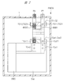
- FIG. 2 is a plan view schematically showing the structure of the power conversion device according to the first embodiment.
- the shape of the first bus bar BSB1 and the second bus bar BSB2, the arrangement and shape of the filter capacitive elements C1, C2, the capacitive elements Cyp1, Cyp2 and the smoothing capacitive element Cxp are drawn in accordance with the actual. Yes.
- each of the first bus bar BSB1 and the second bus bar BSB2 is configured by a flat plate made of a copper material having a predetermined width.
- the main surface of the first bus bar BSB1 extends between the input terminal PP and the smoothing capacitive element Cxp, and has a U-shaped bent portion in the middle.
- the main surface of the second bus bar BSB2 also has a structure extending between the input terminal PN and the smoothing capacitor Cxp and having a U-shaped bent portion in the middle.
- the insulating material is, for example, a gap between the first bus bar BSB1 and the second bus bar BSB2.
- the first bus bar BSB1 and the second bus bar BSB2 constitute a noise filter. It is connected to the capacitor Cx (FIG. 1).
- FIG. 2 only the filter capacitance elements C1 and C2 constituting the capacitance section Cx are depicted as one capacitance block, and one terminal TC11 and TC21 of the filter capacitance elements C1 and C2 are indicated by a circle. And connected to the first bus bar BSB1.
- the other terminals TC12 and TC22 of the filter capacitative elements C1 and C2 are indicated by ⁇ and are connected to the second bus bar BSB2 via resistors R1 and R2 (FIG. 1) (not shown).
- the connection between the first bus bar BSB1 and the second bus bar BSB2, the filter capacitor element and the resistor is not particularly limited, but is performed by fixing with a metal screw.
- the portions of the terminals TC11 and TC21 indicated by ⁇ are fixed to the first bus bar BSB1 with screws.
- the first bus bar BSB1 and the terminals TC11, TC21 of the capacitive elements C1, C2 are electrically connected.
- the other terminals TC12 and TC22 indicated by ⁇ are electrically connected to the second bus bar BSB2 by fixing the terminals TRC1 and TRC2 (FIG. 1) of the resistors R1 and R2 to the second bus bar BSB2 with screws.
- TRC1 and TRC2 FIG. 1
- the terminals TC311 and TC321 of the filter capacitive elements C31 and C32 not shown in FIG. 2 are also screwed into the first bus bar BSB1 and the second bus bar BSB2 in the portions PT1 and PT2 at the same positions as the filter capacitive elements C1 and C2. Fixed and electrically connected. Further, resistors R31 and R32 (not shown) are electrically connected between the housing 1 and the terminals TC312 and TC322 of the filter capacitors C31 and C32.
- Capacitance elements Cyp1 and Cyp2 indicated by circles are fixed to the portions between the bent portions of the first bus bar BSB1 and the second bus bar BSB2 and the smoothing capacitive element Cxp with screws TCy11 and TCy21. Are electrically connected. The other terminals TCy12 and TCy22 of the capacitive elements Cyp1 and Cyp2 are connected to the housing 1.
- the smoothing capacitive element Cxp is larger in size than other capacitive elements when viewed from above.
- the first bus bar BSB1 and the second bus bar BSB2 are not particularly limited, but extend so as to overlap with the pair of electrodes of the smoothing capacitive element Cxp.
- a pair of electrodes of the smoothing capacitive element Cxp includes a plurality of terminals TCx1 and TCx2 indicated by ⁇ , and is fixed to the first bus bar BSB1 and the second bus bar BSB2 arranged in an overlapping manner, and electrically It is connected.
- the first bus bar BSB1 and the second bus bar BSB2 are electrically connected to the switching circuit SWC.
- the input terminals PP and PN are fixed and electrically connected to the cable 2 described in FIG. 1 with screws.
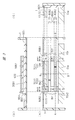
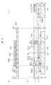
- FIG. 3 is a diagram showing a bus bar structure (bus bar structure) according to the first embodiment.
- FIG. 3A is a top view showing in detail the structure of the first bus bar BSB1 and the second bus bar BSB2.
- 3B is a cross-sectional view showing a cross section A-A ′ in FIG. 3A
- FIG. 3C is a cross-sectional view showing a cross section B-B ′ in FIG.
- FIG. 3 (A), (B), and (C) the broken line which shows a mutual relationship is attached
- the lengths of the first bus bar BSB1 and the second bus bar BSB2 are drawn shorter than those in FIG.
- FIG. 3A the capacitive elements Cyp1 and Cyp2 and the switching circuit SWC illustrated in FIG. 1 are omitted.
- BW1 indicates the width of the first bus bar BSB1
- BW2 indicates the width of the second bus bar BSB2.
- the first bus bar BSB1 and the second bus bar BSB2 have U-shaped bent portions.
- the bus bar BSB1 is bent to the left side and then bent to the right side in the middle of extending from the upper side to the lower side of the drawing, so that a U-shaped bent portion BU1 is formed.
- the second bus bar BSB2 is bent to the right side and bent again to the left side while extending from the upper side to the lower side of the drawing in parallel with the first bus bar BSB1 when viewed from above.
- a U-shaped bent portion BU2 is formed.
- Each of the U-shaped bent portions BU1 and BU2 has a side portion corresponding to the U-shaped side, a bottom portion corresponding to the U-shaped bottom side and connecting the side portions, and a side portion when viewed from above. It can be considered that it is provided with the opening part which is not connecting between.
- the bent portion BU1 formed in the first bus bar BSB1 has a U-shaped shape including an opening on the right side and a bottom portion on the left side in FIG.
- the bent portion BU2 formed on the two bus bars BSB2 has a U-shape having an opening on the left side and a bottom portion on the right side.
- the U-shaped bent portion BU1 formed on the first bus bar BSB1 and the U-shaped bent portion BU2 formed on the second bus bar BSB2 overlap each other when viewed from above. , They are opposite to each other. That is, in the first embodiment, the bent portion BU1 and the bent portion BU2 are arranged so as to overlap when viewed in a plan view, except for the openings of each other.
- an insulating layer formed of an insulating material between the first bus bar BSB1 and the second bus bar BSB2 ISO2 is present.
- the housing 1 is made of a metal material.
- An insulating layer ISO1 is interposed between the second bus bar BSB2 and the housing 1, and an insulating layer ISO2 is interposed between the first bus bar BSB1 and the second bus bar BSB1.
- BD1 and BD2 indicate the thicknesses of the first bus bar BSB1 and the second bus bar BSB2.
- the U-shaped bent portions BU1 and BU2 are arranged so as to be opposite to each other, the opening of one bent portion (for example, the bent portion BU1) is formed in the other bent portion ( It overlaps with the bottom part of BU2) and the respective side parts overlap. As a result, as shown in FIG. 3C, the side portions of the U-shaped bent portions BU1 and BU2 overlap each other.
- the insulating film ISO2 is interposed between the first bus bar BSB1 and the second bus bar BSB2, but is omitted in FIG.
- an insulating layer ISO1 is interposed between the casing 1 and these capacitive elements. is doing.
- the insulating material for forming the insulating layers ISO1 and ISO2 is not particularly limited.
- the bus bars BSB1 and BSB2 and the housing 1 may be physically separated.
- the main surfaces of the first bus bar BSB1 and the second bus bar BSB2 are overlapped at the side portions of the bent portions BU1 and BU2 when viewed from above. It is facing and other parts are arranged so as not to overlap.
- the anode terminal HP is connected to the input terminal PP via the cable 2
- the cathode terminal HN is connected to the input terminal PN via the cable 2. Therefore, the normal mode current (and normal mode noise current) flows in the direction from the input terminal PP toward the input terminal PN in the order of the first bus bar BSB1, the switching circuit SWC, and the second bus bar BSB2.
- a normal mode current flows in a direction from the input terminal PP toward the terminal TCx1 of the smoothing capacitive element Cxp.
- the normal mode current flows in the direction from the terminal TCx2 of the smoothing capacitive element Cxp to the input terminal PN. Therefore, the normal mode current flows in the direction of the solid arrow in the bent portion BU1 of the first bus bar BSB1, and flows in the direction of the alternate long and short dash line in the bent portion BU2 of the second bus bar BSB2.
- normal mode current flows in the same direction in each side portion of the U-shaped bent portions BU1 and BU2.
- the first bus bar BSB1 for example, between the input terminal PP and the terminals TC11 and TC21 are connected between the portion where the terminals TC11 and TC21 of the filter capacitance elements C1 and C2 are connected.
- a normal mode current flows toward the part.
- the second bus bar BSB2 a normal mode current flows from the portion where the terminals TC12 and TC22 are connected toward the input terminal PN. That is, the direction of the normal current that flows between the terminals TC11 and TC21 of the filter capacitors C1 and C2 and the input terminal PP flows between the terminals TC12 and TC22 of the filter capacitors C1 and C2 and the input terminal PN. The direction is opposite to the normal current direction.
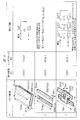
- FIG. 4 is a diagram showing a relationship between the structure of the bus bar and the inductance according to the first embodiment.
- FIG. 4 shows the inductance value measured by the present inventors.
- FIG. 4 shows the structure of the first bus bar BSB1 between the portion connected to the terminals TC11 and TC21 and the portion connected to the terminal TCx1 and the portion connected to the terminals TC12 and TC22 in FIGS.
- the inductance value when the structure of the second bus bar BSB2 between the terminal and the part to which the terminal TCx2 is connected is changed is shown. That is, the inductance value of the inductor portion Lb shown in FIG. 1 is shown.
- the symbol BSB1 (Lb) is assigned to the first bus bar
- the symbol BSB2 (Lb) is assigned to the second bus bar in order to indicate that the bus bar portion corresponds to the inductor portion Lb.
- the first bus bar BSB1 (Lb) and the second bus bar BSB2 (Lb) are overlapped so that the main surfaces face each other when viewed in a plan view.
- the widths BW1 and BW2 of the first bus bar BSB1 (Lb) and the second bus bar BSB2 (Lb) are 30 mm, and the length (the portion of the inductor portion Lb in FIG. 1) is 70 mm.
- the first bus bar BSB1 (Lb) and the second bus bar BSB2 (Lb) are separated by 3 mm.
- each of 1st bus bar BSB1 (Lb) and 2nd bus bar BSB2 (Lb) is comprised with the copper material, and thickness BD1, BD2 is 1.2 mm.
- the “coupling coefficient k2” between the parasitic inductors Lp2 and Ln2 constituting the inductor portion Lb is 0.814.
- a normal mode current flows in the direction of a solid line arrow
- a normal mode current flows in the direction of a one-dot chain line arrow.
- the first bus bar BSB1 (Lb) and the second bus bar BSB2 (Lb) are arranged to extend in parallel.
- a step of 3 mm is provided between the first bus bar BSB1 (Lb) and the second bus bar BSB2 (Lb) so as to occupy the same volume as the “bus bar structure” of number # 1, and is long with a width of 30 mm.
- the first bus bar BSB1 (Lb) and the second bus bar BSB2 (Lb) are arranged within a range of 70 mm.
- the material and thickness of the first bus bar BSB1 (Lb) and the second bus bar BSB2 (Lb) are the same as the “Bus bar structure” of number # 1, except that the widths BW1 and BW2 are 10 mm. .
- the “coupling coefficient k2” between the parasitic inductors Lp2 and Ln2 is 0.418.
- a normal mode current flows in the direction of a solid line arrow
- a normal mode current flows in the direction of a one-dot chain line arrow.
- the normal mode current flowing through the first bus bar BSB1 (Lb) and the normal mode current flowing through the second bus bar BSB2 (Lb) are in opposite directions. Therefore, in the “equivalent circuit”, the directions of the magnetic fields generated by the inductors Lp2 and Ln2 are also reversed, and in the above equation (2), the mutual inductance is a negative value, and the inductance HLb of the inductor portion Lb is small. Therefore, in the “bus bar structure” of number # 1, the inductance HLb of the inductor portion Lb is 10.4 nH, and in the “bus bar structure” of number # 2, the inductance HLb is 46.8 nH.
- the “bus bar structure” with the number # 3 has a U-shaped bent portion as the first bus bar BSB1 (Lb) and the second bus bar BSB2 (Lb). have. Also in the “bus bar structure” of number # 3, the width is 30 mm and long so that the first bus bar BSB1 (Lb) and the second bus bar BSB2 (Lb) are accommodated in the same volume as the numbers # 1 and # 2.
- the first bus bar BSB1 (Lb) and the second bus bar BSB2 (Lb) are arranged within a range of 70 mm.
- the first bus bar BSB1 (Lb) and the second bus bar BSB2 (Lb) are separated by 3 mm.
- the widths BW1, BW2 and the thicknesses BD1, BD2 of the first bus bar BSB1 (Lb) and the second bus bar BSB2 (Lb) are the same as the “bus bar structure” of number # 2.
- the material is also the same copper material.
- the direction in which the normal mode current flows is the same in at least the U-shaped side portion of the bent portion.
- the parasitic inductor Lp2 included in the first bus bar BSB1 (Lb) is considered to be configured by a plurality of partial parasitic inductors (hereinafter also referred to as partial inductors) Lp2-1 to Lp2-3. Can do.
- the parasitic inductor Ln2 included in the second bus bar BSB2 (Lb) can also be regarded as being constituted by a plurality of partial inductors Ln2-1 to Ln2-3.
- the inductance HLb of the inductor portion L2 can be increased. This is because the coupling coefficient k2-1 between the partial inductors Lp2-1 and Ln2-1, the coupling coefficient k2-2 between the partial inductors Lp2-2 and Ln2-2, and the partial inductors Lp2-3 and Ln2-3. This corresponds to a reduction in the overall coupling coefficient, which is the sum of the coupling coefficients k2-3. Thereby, in the bus bar structure according to the first embodiment indicated by the number # 3, the inductance of the inductor portion Lb can be increased to 52.2 nH.
- first bus bar BSB1 (Lb) and the second bus bar BSB2 (Lb) are arranged so that each “bus bar structure” of numbers # 1 to # 3 shown in FIG. 4 occupies the same volume. . That is, it is possible to increase the inductance HLb of the inductor portion L2 while suppressing an increase in size.
- the values of the coupling coefficient k2 and the inductance HLb described with reference to FIG. 4 indicate the case where the frequency of the normal mode current is 10 MHz.
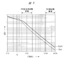
- FIG. 5 is a characteristic diagram showing the attenuation of the LCL (LCLC) filter according to the first embodiment.
- the horizontal axis indicates the frequency F
- the vertical axis indicates the ratio of the voltages V1 and V2 shown in FIG. 13 in decibels (dBV).
- FIG. 14 shows the characteristics when the inductor portion Lb shown in FIG. 13 has the “bus bar structure” of number # 2 in FIG. Also in FIG. 5, the characteristic curve GLb ⁇ b> 1 shows the characteristic when the inductor portion Lb has the “bus bar structure” of number # 2 in FIG. 4.
- the characteristic curve GLp shown in FIG. 2 shows the characteristic curve of an LCL (LCLC) filter with Lb). That is, in FIG. 13, the change with respect to the frequency of the attenuation when the inductor portion Lb has the configuration of the “equivalent circuit” indicated by the number # 3 in FIG. 4 is shown as a characteristic curve GLp.
- the volumes occupied by the first bus bar and the second bus bar when measuring the characteristic curves GLb1 and GLp are the same.
- the first bus bar BSB1 and the second bus bar BSB2 so that the normal mode current flows in the same direction at the opposing portions where the main surfaces face each other in the portion where the inductor portion Lb is formed, Since the inductance in the inductor portion Lb can be increased, the attenuation in the AM broadcast frequency band and the SW frequency band can be increased while suppressing an increase in size. As a result, it is possible to suppress leakage of AM broadcast frequency band and SW frequency band noise from the power conversion device PWCS.
- FIG. 6 is a perspective view showing structures of the first bus bar BSB1 and the second bus bar BSB2 according to the second embodiment.
- the first bus bar BSB1 and the second bus bar BSB2 are arranged three-dimensionally, and at two places, opposing portions whose main surfaces oppose each other are formed.
- BOV1 indicates a first facing portion
- BOV2 indicates a second facing portion.
- the first bus bar BSB1 and the second bus bar BSB2 have a first layer portion extending on the back side (referred to as a first layer for convenience) and a front side (referred to as a second layer for convenience) in the drawing. A second layer portion extending.
- an interlayer connection portion that connects the first layer portion and the second layer portion is formed.
- the interlayer connection part of the first bus bar BSB1 and the interlayer connection part of the second bus bar BSB2 are arranged to face each other.
- the first bus bar BSB1 and the second bus bar BSB2 are arranged so as to overlap and face each other when viewed from above.
- the opposed portion BOV2 is formed.
- the normal mode current indicated by the solid line arrow flowing through the first bus bar BSB1 and the normal mode current indicated by the alternate long and short dash line flowing through the second bus bar BSB2 are in the same direction in the first opposing part BOV1 and the second opposing part BOV2. It begins to flow.
- the direction in which the normal mode current flows is reversed. It has become.
- FIG. 7 shows the structure of the bus bar according to the second embodiment.
- FIG. 7A is a top view showing in detail the structure of first bus bar BSB1 and second bus bar BSB2 shown in FIG. 7B is a cross-sectional view showing a cross section A-A ′ of FIG. 7A
- FIG. 7C is a cross-sectional view showing a cross section B-B ′ of FIG. 7A.
- FIG. 7 (A), (B), and (C) the broken line which shows a mutual relationship is attached
- the lengths of the first bus bar BSB1 and the second bus bar BSB2 are drawn shorter than those in FIG. 6 in order to make the drawing easier to see, as in FIG.
- the first bus bar BSB1 and the second bus bar BSB2 shown are the same as in FIG. Since FIG. 7 is similar to FIG. 4, only the differences will be mainly described.
- the first bus bar BSB1 and the second bus bar BSB2 do not overlap when viewed from the upper surface side.
- a part of the main surface of the first bus bar BSB1 and a part of the main surface of the second bus bar BSB2 are arranged to face each other.
- the impedance at this part can be increased.
- the first bus bar BSB1 overlaps the second bus bar BSB2, and the main surface of the second bus bar BSB1 and the main surface of the second bus bar BSB2 face each other. Yes.
- the impedance in this portion can be increased.
- the interlayer connection portion may be a bent portion of the first bus bar BSB1 and the second bus bar BSB2.
- FIG. 8 is a diagram showing the structure of the bus bar according to the third embodiment.
- FIG. 8A is a top view showing the structure of the first bus bar BSB1 and the second bus bar BSB2.
- FIG. 8B is a cross-sectional view showing a cross-section A-A ′ of FIG. 8A
- FIG. 8C is a cross-sectional view showing a cross-section B-B ′ of FIG.
- FIG. 8 (A), (B), and (C) the broken line which shows a mutual relationship is attached
- each of the first bus bar BSB1 and the second bus bar BSB2 includes L-shaped bent portions BL1 and BL2 when viewed from above. That is, as shown in FIG. 8A, the first bus bar BSB1 extends from the upper side to the lower side, and bends to the left side in the middle to form an L-shaped bent portion BL1. Thereafter, it extends downward again and is connected to the smoothing capacitive element Cxp.
- the second bus bar BSB2 extends from the upper side to the lower side in parallel with the first bus bar BSB1, and is bent to the right side in the middle to form an L-shaped bent portion BL2. Thereafter, it extends downward again and is connected to the smoothing capacitive element Cxp.
- the main surfaces of the first bus bar BSB1 and the second bus bar BSB2 overlap each other.
- the normal mode current flows through the first bus bar BSB1 in the direction indicated by the solid line arrow, and flows through the second bus bar BSB2 in the direction indicated by the alternate long and short dash line arrow.
- the main surfaces of the first bus bar BSB1 and the second bus bar BSB2 are opposed to each other, so that the normal mode current flows in the same direction, thereby increasing the inductance in the opposed portion.
- the first bus bar BSB1 is formed on the housing 1 side with respect to the second bus bar BSB2.
- the second bus bar BSB2 is It may be formed close to the housing 1 side.
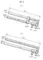
- FIG. 9 is a perspective view showing the structure of the bus bar according to the fourth embodiment.
- FIG. 9A is a perspective view showing a bus bar structure in which the first bus bar BSB1 and the second bus bar BSB2 are provided with bent portions having different shapes.
- the input terminals PP and PN are arranged on the upper side of the housing 1.
- the input terminals PP and PN are arranged on the left side of the housing 1 shown in FIG.
- the first bus bar BSB1 includes a bent portion that extends from the input terminal PP disposed on the left side of the housing 1 toward the right side and is then bent into a Z shape. ing. After bending in the Z shape, the first bus bar BSB1 is connected to the terminal TCx2 of the smoothing capacitive element Cxp.
- the second bus bar BSB2 extends from the input terminal PN toward the right side, is bent in a U shape, and is bent in an L shape.
- a part of the Z-shaped bent part in the first bus bar BSB1 and a part of the L-shaped bent part in the second bus bar BSB2 overlap when viewed from above, and the first opposing part BOV3 is formed. Further, a part of the Z-shaped bent part in the first bus bar BSB1 and a part of the U-shaped bent part in the second bus bar BSB2 overlap each other when viewed from above, and the second facing part BOV4. Will be formed.
- the first opposing part BOV3 and the second opposing part BOV4 Since the direction of the normal mode current flowing through the first bus bar BSB1 and the second bus bar BSB2 is the same in each of the first opposing part BOV3 and the second opposing part BOV4, the first opposing part BOV3 and the second opposing part It is possible to increase the inductance in the part BOV4. Also in the fourth embodiment, the solid arrow indicates the direction of the normal mode current flowing through the first bus bar BSB1, and the alternate long and short dash line indicates the direction of the normal mode current flowing through the second bus bar BSB2.
- the lateral length BL1 of the first bus bar BSB1 and the second bus bar BSB2 is 160 mm, for example, and the width, thickness and material of the first bus bar BSB1 and the second bus bar BSB2 are described with reference to number # 3 in FIG.
- the inductance of the first bus bar BSB1 is 126.83 nH
- the inductance of the second bus bar BSB2 is 123.45 nH.
- the coupling coefficient at this time is 0.36
- the overall inductance is 158.4 nH. Note that the frequency of the normal mode current at this time is 10 MHz.
- FIG. 9B shows a case where a bent portion is provided in the first bus bar BSB1 and the second bus bar BSB2 so that only one facing portion is formed.
- the first bus bar BSB1 extends rightward and then bends in an L shape.
- the second bus bar BSB2 is bent in an L shape and further bent in an L shape.
- FIG. 9B when a part of the L-shaped bent part in the first bus bar BSB1 and a part of the second L-shaped bent part in the second bus bar BSB2 are viewed in a top view.
- an opposing portion BOV5 is formed.
- the facing portion BOV5 the direction of the normal mode current flowing through the first bus bar BSB1 and the second bus bar BSB2 is the same, so that the inductance can be increased in the facing portion BOV5.
- the width, thickness, and material of the first bus bar BSB1 and the second bus bar BSB2 shown in FIG. 9B are the same as those of the first bus bar BSB1 and the second bus bar BSB2 shown in FIG.
- the lateral length BL2 of the first bus bar BSB1 and the second bus bar BSB2 is 176 mm. That is, since there are few facing parts, the inductance performance is about 10% lower than the shape shown in FIG. 9A, and the bus bar length BL2 is required to be about 10% longer. In other words, it is possible to reduce the size by increasing the number of facing portions.
- the inductance of the first bus bar BSB1 shown in FIG. 9B is 140.7 nH
- the inductance of the second bus bar BSB2 is 128.6 nH.
- the coupling coefficient is 0.41.
- connection between the first bus bar BSB1 and the second bus bar BSB2 and the terminal of the capacitive element may be a connection using solder or the like instead of a metallic screw.
Landscapes
- Engineering & Computer Science (AREA)
- Power Engineering (AREA)
- Physics & Mathematics (AREA)
- Electromagnetism (AREA)
- Inverter Devices (AREA)
- Power Conversion In General (AREA)
- Electric Propulsion And Braking For Vehicles (AREA)
Abstract
Description
<ノイズフィルタ>
本発明者らは、ノーマルモードノイズ電流を低減して、AM放送周波数帯域およびSW周波数帯域のノイズを抑制するために、バスバにノイズフィルタを結合することを考えた。すなわち、電力変換装置の陽極用電源入力端子とスイッチング素子との間を電気的に接続するバスバと、陰極用電源入力端子とスイッチング素子との間を電気的に接続するバスバに容量部を結合することを考えた。この場合、容量部は、例えば、バスバ間に接続された容量素子と、それぞれのバスバとフレームグランドとの間に接続された容量素子によって構成する。バスバは、例えば銅板によって構成されるため、寄生のインダクタを有する。そのため、容量部とバスバのインダクタによってノイズフィルタが構成されることになる。


図1は、実施の形態1に係わる電力変換装置の構成を示すブロック図である。同図において、1は電力変換装置PWCSの筐体を示している。この筐体1に、種々の回路ブロックおよび素子が格納されて、電力変換装置PWCSが構成されている。図1では、筐体1に格納された回路ブロックおよび素子のうち、説明に必要なもののみが描かれている。また、同図には、電力変換装置PWCSへ直流電圧を給電する高電圧バッテリHVBTと電力変換装置PWCSによって形成された交流電圧によって駆動される電気モータ4とが示されている。
図2は、実施の形態1に係わる電力変換装置の構造を模式的に示す平面図である。同図には、電力変換装置PWCSの筐体1に格納されている回路ブロックおよび部品のうち、第1バスバBSB1、第2バスバBSB2、フィルタ用容量素子C1、C2、容量素子Cyp1、Cyp2、平滑用容量素子Cxpおよびスイッチング回路SWCのみが描かれており、他の部分は省略されている。模式的ではあるが、第1バスバBSB1および第2バスバBSB2の形状、フィルタ用容量素子C1、C2、容量素子Cyp1、Cyp2および平滑用容量素子Cxpの配置および形状は、実際に合わせて描かれている。
図6は、実施の形態2に係わる第1バスバBSB1および第2バスバBSB2の構造を示す斜視図である。この実施の形態2において、第1バスバBSB1と第2バスバBSB2は、3次元的に配置され、2箇所において、互いに主面が対向する対向部が形成されている。同図において、BOV1は第1の対向部を示し、BOV2は第2の対向部を示している。
実施の形態1および2においては、第1バスバBSB1および第2バスバBSB2が、複数の対向部を備えている例を示したが、これに限定されるものではない。実施の形態3においては、1個の対向部を備えたバスバ構造が提供される。
実施の形態1では、第1バスバBSB1と第2バスバBSB2が、同じU字状の屈曲部を有する例を説明した。しかしながら、第1バスバBSB1と第2バスバBSB2とが同じ形状の屈曲部を備えていなくてもよい。
2、3 ケーブル
4 電気モータ
BSB1 第1バスバ
BSB2 第2バスバ
C1、C2 フィルタ用容量素子
Cxp 平滑用容量素子
HVBT 高電圧バッテリ
SWC スイッチング回路
Claims (12)
- 電源の陽極端子と陰極端子との間に接続され、直流電圧に重畳する電圧変化を平滑化する第1容量部と、
前記直流電圧を交流電圧に変換するスイッチング回路と、
前記電源の陽極端子と前記第1容量部の第1端子との間を電気的に接続する第1バスバと、
前記電源の陰極端子と前記第1容量部の第2端子との間を電気的に接続する第2バスバと、
前記第1バスバと前記第2バスバとの間に電気的に接続された第2容量部と、
を備え、
前記第1バスバと前記第2バスバは、互いに対向する対向部を有し、前記対向部において流れる電流の方向が同じとなるように配置されている、電力変換装置。 - 請求項1に記載の電力変換装置において、
前記電力変換装置は、ケーブルを介して前記陽極端子および前記陰極端子に接続される第1電源入力端子および第2電源入力端子を備え、
前記第1バスバは前記第1電源入力端子と前記第1容量部の第1端子との間に接続され、前記第2バスバは前記第2電源入力端子と前記第1容量部の第2端子との間に接続され、
前記第2容量部は、前記第1バスバにおいて前記第1電源入力端子と前記第1容量部の第1端子との間の第1部分に接続された第1端子と、前記第2バスバにおいて前記第2電源入力端子と前記第1容量部の第2端子との間の第2部分に接続された第2端子とを備え、
前記第1バスバは、前記第2容量部の第1端子が接続された部分と前記第1部分との間において、前記対向部を備え、前記第2バスバは、前記第2容量部の第2端子が接続された部分と前記第2部分との間において、前記対向部を備える、電力変換装置。 - 請求項2に記載の電力変換装置において、
前記第1バスバは、前記第1電源入力端子と前記第1部分との間で形成された等価的な第1インダクタ部と、前記第1部分と前記第1容量部の第1端子が接続された部分との間で形成された等価的な第2インダクタ部とを備え、
前記第2バスバは、前記第2電源入力端子と前記第2部分との間で形成された等価的な第3インダクタ部と、前記第2部分と前記第1容量部の第2端子が接続された部分との間で形成された等価的な第4インダクタ部とを備え、
前記電力変換装置は、前記第1インダクタ部、前記第3インダクタ部および前記第2容量部を有する第1フィルタ回路と、前記第2インダクタ部、前記第4インダクタ部および前記第1容量部を有し、前記第1フィルタ回路と直列的に結合された第2フィルタ回路を備える、電力変換装置。 - 請求項1から3のいずれか一つに記載の電力変換装置において、
前記第1バスバおよび前記第2バスバは、前記対向部において、それぞれの主面が対向するように配置されている、電力変換装置。 - 請求項4に記載の電力変換装置において、
前記第1バスバおよび前記第2バスバのそれぞれは、U字状の屈曲部を備え、U字状の屈曲部が逆向きで、離間して対向するように配置されている、電力変換装置。 - 電源の陽極端子および陰極端子と、直流電圧を交流電圧に変換するスイッチング回路との間を電気的に結合する第1バスバおよび第2バスバを備えたバスバ構造であって、
前記第1バスバおよび前記第2バスバは、フィルタ用容量部の端子が結合される部分と前記スイッチング回路が結合される部分との間で、同じ方向に電流が流れるように、対向して配置された対向部を備えている、バスバ構造。 - 請求項6に記載のバスバ構造において、
前記第1バスバと前記第2バスバとの間には、前記直流電圧に重畳される電圧変化を平滑化する平滑用容量部が結合され、
前記対向部は、前記フィルタ用容量部の端子が結合される部分と、前記平滑用容量部が結合される部分との間に配置される、バスバ構造。 - 請求項6または7に記載のバスバ構造において、
前記第1バスバおよび前記第2バスバは、前記対向部において、それぞれの主面が対向するように配置されている、バスバ構造。 - 請求項8に記載のバスバ構造において、
前記第1バスバおよび前記第2バスバのそれぞれは、U字状の屈曲部を備え、U字状の屈曲部が逆向きで、離間して対向するように配置されている、バスバ構造。 - 電源の陽極端子および陰極端子とスイッチング回路との間を電気的に接続する第1バスバおよび第2バスバと、
前記第1バスバにおける第1部分と前記第2バスバにおける第2部分との間に結合されたフィルタ用容量部と、
前記第1バスバおよび前記第2バスバにおいて、前記第1部分および前記第2部分と前記スイッチング回路が結合された部分との間であって、前記第1バスバと前記第2バスバとの間に結合された平滑用容量部と、
を備え、
前記電源の陽極端子から陰極端子に向けて電流が流れたとき、前記第1バスバにおける前記第1部分と前記平滑用容量部が結合された部分との間の部分と、前記第2バスバにおける前記第2部分と前記平滑用容量部が結合された部分との間の部分において、同じ方向の磁界を発生する部分を備えている、電力変換装置。 - 請求項10に記載の電力変換装置において、
同じ方向の磁界を発生する部分において、前記第1バスバの主面と前記第2バスバの主面は対向している、電力変換装置。 - 請求項11に記載の電力変換装置において、
前記電源の陽極端子から陰極端子に向けて電流が流れたとき、前記第1バスバにおいて前記陽極端子が結合された部分と前記第1部分との間と、前記第2バスバにおいて前記陽極端子が結合された部分と前記第2部分との間において、逆方向の磁界を発生する部分を、前記第1バスバおよび前記第2バスバは備えている、電力変換装置。
Priority Applications (3)
| Application Number | Priority Date | Filing Date | Title |
|---|---|---|---|
| DE112017005722.1T DE112017005722B4 (de) | 2016-12-13 | 2017-10-17 | Sammelschienenstruktur und Leistungswandlungsvorrichtung, welche diese verwendet |
| US16/469,000 US11043906B2 (en) | 2016-12-13 | 2017-10-17 | Bus bar structure and power conversion apparatus using the same |
| CN201780076928.XA CN110168903B (zh) | 2016-12-13 | 2017-10-17 | 母排构造和使用它的电力变换装置 |
Applications Claiming Priority (2)
| Application Number | Priority Date | Filing Date | Title |
|---|---|---|---|
| JP2016-240845 | 2016-12-13 | ||
| JP2016240845A JP6643972B2 (ja) | 2016-12-13 | 2016-12-13 | バスバ構造およびそれを用いた電力変換装置 |
Publications (1)
| Publication Number | Publication Date |
|---|---|
| WO2018110071A1 true WO2018110071A1 (ja) | 2018-06-21 |
Family
ID=62559414
Family Applications (1)
| Application Number | Title | Priority Date | Filing Date |
|---|---|---|---|
| PCT/JP2017/037542 Ceased WO2018110071A1 (ja) | 2016-12-13 | 2017-10-17 | バスバ構造およびそれを用いた電力変換装置 |
Country Status (5)
| Country | Link |
|---|---|
| US (1) | US11043906B2 (ja) |
| JP (1) | JP6643972B2 (ja) |
| CN (1) | CN110168903B (ja) |
| DE (1) | DE112017005722B4 (ja) |
| WO (1) | WO2018110071A1 (ja) |
Cited By (3)
| Publication number | Priority date | Publication date | Assignee | Title |
|---|---|---|---|---|
| JP2021182841A (ja) * | 2020-05-20 | 2021-11-25 | 株式会社日立製作所 | ノイズフィルタ、電力変換装置 |
| EP3934091A4 (en) * | 2019-03-01 | 2022-03-02 | Mitsubishi Electric Corporation | CURRENT TRANSFORMING DEVICE |
| WO2023036564A1 (de) * | 2021-09-10 | 2023-03-16 | Auto-Kabel Management Gmbh | Anschlussteil mit doppelten stromschienen |
Families Citing this family (9)
| Publication number | Priority date | Publication date | Assignee | Title |
|---|---|---|---|---|
| RU2697503C1 (ru) * | 2016-06-02 | 2019-08-15 | Ниссан Мотор Ко., Лтд. | Устройство преобразования мощности |
| CN107508455A (zh) * | 2017-08-25 | 2017-12-22 | 惠科股份有限公司 | 缓冲电路及其显示装置 |
| JP2020088888A (ja) * | 2018-11-15 | 2020-06-04 | 株式会社日立製作所 | 電圧フィルタおよび電力変換装置 |
| JP7280092B2 (ja) * | 2019-04-02 | 2023-05-23 | 双信電機株式会社 | ノイズフィルタ装置 |
| DE102019123197A1 (de) * | 2019-06-25 | 2020-12-31 | Tdk Electronics Ag | Elektrische Komponente |
| JP7363599B2 (ja) * | 2020-03-09 | 2023-10-18 | トヨタ自動車株式会社 | 車両用電源システム |
| JP7577987B2 (ja) * | 2020-12-07 | 2024-11-06 | 株式会社Ihi | 電力変換装置 |
| JP7678642B2 (ja) * | 2021-04-12 | 2025-05-16 | Astemo株式会社 | フィルタ装置及び電力変換装置 |
| JPWO2023079617A1 (ja) * | 2021-11-04 | 2023-05-11 |
Citations (3)
| Publication number | Priority date | Publication date | Assignee | Title |
|---|---|---|---|---|
| JP2000069766A (ja) * | 1998-08-24 | 2000-03-03 | Hitachi Ltd | 電力変換装置 |
| JP2006060876A (ja) * | 2004-08-17 | 2006-03-02 | Fuji Electric Holdings Co Ltd | コンデンサとその設置方法 |
| JP2009105178A (ja) * | 2007-10-23 | 2009-05-14 | Nichicon Corp | パワー半導体ユニット |
Family Cites Families (24)
| Publication number | Priority date | Publication date | Assignee | Title |
|---|---|---|---|---|
| DE19732402B4 (de) * | 1997-07-28 | 2004-07-15 | Danfoss Drives A/S | Elektrische Busanordnung zur Gleichstromversorgung von Schaltungselementen eines Wechselrichters |
| JP3424532B2 (ja) * | 1997-11-25 | 2003-07-07 | 株式会社日立製作所 | 電力変換装置 |
| RU2190919C2 (ru) * | 1998-04-28 | 2002-10-10 | Хитачи, Лтд. | Силовая цепь электрического силового преобразователя |
| EP1742265B1 (en) * | 2000-04-19 | 2013-08-07 | Denso Corporation | Coolant cooled type semiconductor device |
| JP2005237118A (ja) * | 2004-02-19 | 2005-09-02 | Toyota Motor Corp | バスバー構造体とそれが利用されている電力変換装置 |
| JP2007053839A (ja) | 2005-08-17 | 2007-03-01 | Toshiba Corp | スナバ回路及びこれを用いた電力変換装置 |
| JP4525554B2 (ja) * | 2005-10-21 | 2010-08-18 | 株式会社デンソー | 電流センサ |
| JP4859443B2 (ja) * | 2005-11-17 | 2012-01-25 | 日立オートモティブシステムズ株式会社 | 電力変換装置 |
| US7547987B2 (en) * | 2006-06-22 | 2009-06-16 | Hitachi, Ltd | EMI reduced power inverter |
| US7547848B2 (en) * | 2007-03-23 | 2009-06-16 | International Business Machines Corporation | Structure and method for a twisted bus bar for low impedance power distribution and electromagnetic field suppression |
| JP4561874B2 (ja) * | 2008-05-20 | 2010-10-13 | 株式会社豊田自動織機 | 電力変換装置 |
| JP4973697B2 (ja) * | 2009-06-29 | 2012-07-11 | 株式会社デンソー | 電力変換装置 |
| JP5336413B2 (ja) * | 2010-04-02 | 2013-11-06 | 株式会社豊田中央研究所 | パワーモジュール |
| JP5700022B2 (ja) * | 2012-10-29 | 2015-04-15 | 株式会社デンソー | 電力変換装置 |
| JP6214024B2 (ja) * | 2012-11-16 | 2017-10-18 | 北川工業株式会社 | バスバーアセンブリ |
| JP6416250B2 (ja) * | 2014-06-06 | 2018-10-31 | 日立オートモティブシステムズ株式会社 | 電力変換装置 |
| DE102014111421A1 (de) * | 2014-08-11 | 2016-02-11 | Woodward Kempen Gmbh | Niederinduktive Schaltungsanordnung eines Umrichters |
| WO2016084136A1 (ja) * | 2014-11-25 | 2016-06-02 | ルビコン株式会社 | 四端子スナバコンデンサ及びコンデンサモジュール |
| US9825522B2 (en) * | 2015-04-09 | 2017-11-21 | Ford Global Technologies, Llc | Method and apparatus for coupling cancellation |
| WO2016186101A1 (ja) * | 2015-05-18 | 2016-11-24 | カルソニックカンセイ株式会社 | 電力変換装置 |
| EP3185660A1 (de) * | 2015-12-22 | 2017-06-28 | Siemens Aktiengesellschaft | Stromschienenanordnung |
| US10277116B2 (en) * | 2016-03-31 | 2019-04-30 | Kabushiki Kaisha Toyota Jidoshokki | On-vehicle power conversion apparatus |
| CN105939554B (zh) * | 2016-06-03 | 2018-02-09 | 杭州士兰微电子股份有限公司 | Led调光装置及led驱动电源 |
| DE112017004401B4 (de) * | 2016-09-02 | 2024-05-08 | Mitsubishi Electric Corporation | Stromschienenstruktur und leistungswandlervorrichtung unter verwendung der stromschienenstruktur |
-
2016
- 2016-12-13 JP JP2016240845A patent/JP6643972B2/ja active Active
-
2017
- 2017-10-17 US US16/469,000 patent/US11043906B2/en active Active
- 2017-10-17 DE DE112017005722.1T patent/DE112017005722B4/de active Active
- 2017-10-17 CN CN201780076928.XA patent/CN110168903B/zh active Active
- 2017-10-17 WO PCT/JP2017/037542 patent/WO2018110071A1/ja not_active Ceased
Patent Citations (3)
| Publication number | Priority date | Publication date | Assignee | Title |
|---|---|---|---|---|
| JP2000069766A (ja) * | 1998-08-24 | 2000-03-03 | Hitachi Ltd | 電力変換装置 |
| JP2006060876A (ja) * | 2004-08-17 | 2006-03-02 | Fuji Electric Holdings Co Ltd | コンデンサとその設置方法 |
| JP2009105178A (ja) * | 2007-10-23 | 2009-05-14 | Nichicon Corp | パワー半導体ユニット |
Cited By (6)
| Publication number | Priority date | Publication date | Assignee | Title |
|---|---|---|---|---|
| EP3934091A4 (en) * | 2019-03-01 | 2022-03-02 | Mitsubishi Electric Corporation | CURRENT TRANSFORMING DEVICE |
| US11699959B2 (en) | 2019-03-01 | 2023-07-11 | Mitsubishi Electric Corporation | Power conversion device |
| JP2021182841A (ja) * | 2020-05-20 | 2021-11-25 | 株式会社日立製作所 | ノイズフィルタ、電力変換装置 |
| WO2021235150A1 (ja) * | 2020-05-20 | 2021-11-25 | 株式会社日立製作所 | ノイズフィルタ、電力変換装置 |
| JP7506522B2 (ja) | 2020-05-20 | 2024-06-26 | 株式会社日立製作所 | ノイズフィルタ、電力変換装置 |
| WO2023036564A1 (de) * | 2021-09-10 | 2023-03-16 | Auto-Kabel Management Gmbh | Anschlussteil mit doppelten stromschienen |
Also Published As
| Publication number | Publication date |
|---|---|
| DE112017005722B4 (de) | 2025-12-04 |
| US20190312522A1 (en) | 2019-10-10 |
| US11043906B2 (en) | 2021-06-22 |
| DE112017005722T5 (de) | 2019-08-08 |
| JP6643972B2 (ja) | 2020-02-12 |
| CN110168903A (zh) | 2019-08-23 |
| JP2018098891A (ja) | 2018-06-21 |
| CN110168903B (zh) | 2020-11-13 |
Similar Documents
| Publication | Publication Date | Title |
|---|---|---|
| JP6643972B2 (ja) | バスバ構造およびそれを用いた電力変換装置 | |
| US10979014B2 (en) | Voltage filter and power conversion device | |
| JP6602474B2 (ja) | 半導体装置および電力変換装置 | |
| JP6041583B2 (ja) | 電力変換装置 | |
| CN115699550B (zh) | 噪声滤波器及使用该噪声滤波器的电力转换装置 | |
| JP5235820B2 (ja) | 電力変換装置 | |
| JP7496434B2 (ja) | 電力変換装置 | |
| JP5134934B2 (ja) | 低ノイズ電力変換装置 | |
| CN112514224B (zh) | 高电压滤波器和电力转换装置 | |
| JP6447789B1 (ja) | ノイズフィルタ | |
| JP6528385B2 (ja) | 電力変換装置 | |
| JP7454952B2 (ja) | ノイズフィルタおよび電力変換装置 | |
| KR102702956B1 (ko) | 전자기 간섭 억제 컴포넌트 | |
| CN115516762B (zh) | 滤波装置及电力变换装置 | |
| CN108496303B (zh) | 电路装置 | |
| JP2010193546A (ja) | アクチュエータ駆動回路 | |
| JP7634461B2 (ja) | コンデンサモジュールおよび電力変換装置 | |
| WO2022219925A1 (ja) | フィルタ装置及び電力変換装置 | |
| JP6563081B1 (ja) | 電力変換装置 | |
| JP7802495B2 (ja) | 電力変換装置及びその製造方法 | |
| JP7095711B2 (ja) | スイッチング電源装置 | |
| CN109661708B (zh) | 扼流线圈 | |
| JP2014082845A (ja) | 回路装置 | |
| JP2016019458A (ja) | 電力変換装置 |
Legal Events
| Date | Code | Title | Description |
|---|---|---|---|
| 121 | Ep: the epo has been informed by wipo that ep was designated in this application |
Ref document number: 17881629 Country of ref document: EP Kind code of ref document: A1 |
|
| WWE | Wipo information: entry into national phase |
Ref document number: 112017005722 Country of ref document: DE |
|
| WWP | Wipo information: published in national office |
Ref document number: 112017005722 Country of ref document: DE |
|
| 122 | Ep: pct application non-entry in european phase |
Ref document number: 17881629 Country of ref document: EP Kind code of ref document: A1 |
|
| WWG | Wipo information: grant in national office |
Ref document number: 112017005722 Country of ref document: DE |