WO2018105474A1 - Dispositif d'imagerie à semi-conducteurs et dispositif d'imagerie - Google Patents
Dispositif d'imagerie à semi-conducteurs et dispositif d'imagerie Download PDFInfo
- Publication number
- WO2018105474A1 WO2018105474A1 PCT/JP2017/042988 JP2017042988W WO2018105474A1 WO 2018105474 A1 WO2018105474 A1 WO 2018105474A1 JP 2017042988 W JP2017042988 W JP 2017042988W WO 2018105474 A1 WO2018105474 A1 WO 2018105474A1
- Authority
- WO
- WIPO (PCT)
- Prior art keywords
- sensitivity
- signal
- pixel
- low
- frame
- Prior art date
Links
- 238000003384 imaging method Methods 0.000 title claims abstract description 123
- 230000035945 sensitivity Effects 0.000 claims abstract description 393
- 238000012545 processing Methods 0.000 claims abstract description 54
- 238000006243 chemical reaction Methods 0.000 claims abstract description 29
- 238000012937 correction Methods 0.000 claims description 87
- 238000009792 diffusion process Methods 0.000 claims description 53
- 238000012546 transfer Methods 0.000 claims description 29
- 239000011159 matrix material Substances 0.000 claims description 12
- 238000000034 method Methods 0.000 claims description 3
- 230000002194 synthesizing effect Effects 0.000 claims description 3
- 238000010586 diagram Methods 0.000 description 68
- 230000007274 generation of a signal involved in cell-cell signaling Effects 0.000 description 31
- 230000000875 corresponding effect Effects 0.000 description 29
- 230000015572 biosynthetic process Effects 0.000 description 26
- 238000003786 synthesis reaction Methods 0.000 description 26
- 230000001629 suppression Effects 0.000 description 16
- 238000009825 accumulation Methods 0.000 description 12
- 230000003321 amplification Effects 0.000 description 11
- 238000003199 nucleic acid amplification method Methods 0.000 description 11
- 230000006870 function Effects 0.000 description 10
- 238000001514 detection method Methods 0.000 description 7
- 238000005096 rolling process Methods 0.000 description 7
- 230000008859 change Effects 0.000 description 5
- 230000005484 gravity Effects 0.000 description 4
- 230000004044 response Effects 0.000 description 4
- 229920006395 saturated elastomer Polymers 0.000 description 4
- 230000002596 correlated effect Effects 0.000 description 3
- 238000005286 illumination Methods 0.000 description 3
- 238000012986 modification Methods 0.000 description 3
- 230000004048 modification Effects 0.000 description 3
- 230000001276 controlling effect Effects 0.000 description 2
- 239000002184 metal Substances 0.000 description 2
- 239000002131 composite material Substances 0.000 description 1
- 230000006835 compression Effects 0.000 description 1
- 238000007906 compression Methods 0.000 description 1
- 238000012790 confirmation Methods 0.000 description 1
- 239000000470 constituent Substances 0.000 description 1
- 230000002950 deficient Effects 0.000 description 1
- 238000013461 design Methods 0.000 description 1
- 239000000284 extract Substances 0.000 description 1
- 210000003127 knee Anatomy 0.000 description 1
- 230000007935 neutral effect Effects 0.000 description 1
- 230000009467 reduction Effects 0.000 description 1
- 238000005070 sampling Methods 0.000 description 1
Images


Classifications
-
- H—ELECTRICITY
- H01—ELECTRIC ELEMENTS
- H01L—SEMICONDUCTOR DEVICES NOT COVERED BY CLASS H10
- H01L27/00—Devices consisting of a plurality of semiconductor or other solid-state components formed in or on a common substrate
- H01L27/14—Devices consisting of a plurality of semiconductor or other solid-state components formed in or on a common substrate including semiconductor components sensitive to infrared radiation, light, electromagnetic radiation of shorter wavelength or corpuscular radiation and specially adapted either for the conversion of the energy of such radiation into electrical energy or for the control of electrical energy by such radiation
- H01L27/144—Devices controlled by radiation
- H01L27/146—Imager structures
- H01L27/14601—Structural or functional details thereof
- H01L27/14603—Special geometry or disposition of pixel-elements, address-lines or gate-electrodes
- H01L27/14605—Structural or functional details relating to the position of the pixel elements, e.g. smaller pixel elements in the center of the imager compared to pixel elements at the periphery
-
- H—ELECTRICITY
- H01—ELECTRIC ELEMENTS
- H01L—SEMICONDUCTOR DEVICES NOT COVERED BY CLASS H10
- H01L27/00—Devices consisting of a plurality of semiconductor or other solid-state components formed in or on a common substrate
- H01L27/14—Devices consisting of a plurality of semiconductor or other solid-state components formed in or on a common substrate including semiconductor components sensitive to infrared radiation, light, electromagnetic radiation of shorter wavelength or corpuscular radiation and specially adapted either for the conversion of the energy of such radiation into electrical energy or for the control of electrical energy by such radiation
- H01L27/142—Energy conversion devices
-
- H—ELECTRICITY
- H04—ELECTRIC COMMUNICATION TECHNIQUE
- H04N—PICTORIAL COMMUNICATION, e.g. TELEVISION
- H04N17/00—Diagnosis, testing or measuring for television systems or their details
- H04N17/002—Diagnosis, testing or measuring for television systems or their details for television cameras
-
- H—ELECTRICITY
- H04—ELECTRIC COMMUNICATION TECHNIQUE
- H04N—PICTORIAL COMMUNICATION, e.g. TELEVISION
- H04N23/00—Cameras or camera modules comprising electronic image sensors; Control thereof
- H04N23/50—Constructional details
- H04N23/54—Mounting of pick-up tubes, electronic image sensors, deviation or focusing coils
-
- H—ELECTRICITY
- H04—ELECTRIC COMMUNICATION TECHNIQUE
- H04N—PICTORIAL COMMUNICATION, e.g. TELEVISION
- H04N23/00—Cameras or camera modules comprising electronic image sensors; Control thereof
- H04N23/50—Constructional details
- H04N23/55—Optical parts specially adapted for electronic image sensors; Mounting thereof
-
- H—ELECTRICITY
- H04—ELECTRIC COMMUNICATION TECHNIQUE
- H04N—PICTORIAL COMMUNICATION, e.g. TELEVISION
- H04N23/00—Cameras or camera modules comprising electronic image sensors; Control thereof
- H04N23/70—Circuitry for compensating brightness variation in the scene
- H04N23/73—Circuitry for compensating brightness variation in the scene by influencing the exposure time
-
- H—ELECTRICITY
- H04—ELECTRIC COMMUNICATION TECHNIQUE
- H04N—PICTORIAL COMMUNICATION, e.g. TELEVISION
- H04N23/00—Cameras or camera modules comprising electronic image sensors; Control thereof
- H04N23/80—Camera processing pipelines; Components thereof
-
- H—ELECTRICITY
- H04—ELECTRIC COMMUNICATION TECHNIQUE
- H04N—PICTORIAL COMMUNICATION, e.g. TELEVISION
- H04N25/00—Circuitry of solid-state image sensors [SSIS]; Control thereof
- H04N25/50—Control of the SSIS exposure
- H04N25/53—Control of the integration time
-
- H—ELECTRICITY
- H04—ELECTRIC COMMUNICATION TECHNIQUE
- H04N—PICTORIAL COMMUNICATION, e.g. TELEVISION
- H04N25/00—Circuitry of solid-state image sensors [SSIS]; Control thereof
- H04N25/50—Control of the SSIS exposure
- H04N25/57—Control of the dynamic range
-
- H—ELECTRICITY
- H04—ELECTRIC COMMUNICATION TECHNIQUE
- H04N—PICTORIAL COMMUNICATION, e.g. TELEVISION
- H04N25/00—Circuitry of solid-state image sensors [SSIS]; Control thereof
- H04N25/50—Control of the SSIS exposure
- H04N25/57—Control of the dynamic range
- H04N25/58—Control of the dynamic range involving two or more exposures
- H04N25/581—Control of the dynamic range involving two or more exposures acquired simultaneously
- H04N25/583—Control of the dynamic range involving two or more exposures acquired simultaneously with different integration times
-
- H—ELECTRICITY
- H04—ELECTRIC COMMUNICATION TECHNIQUE
- H04N—PICTORIAL COMMUNICATION, e.g. TELEVISION
- H04N25/00—Circuitry of solid-state image sensors [SSIS]; Control thereof
- H04N25/50—Control of the SSIS exposure
- H04N25/57—Control of the dynamic range
- H04N25/58—Control of the dynamic range involving two or more exposures
- H04N25/581—Control of the dynamic range involving two or more exposures acquired simultaneously
- H04N25/585—Control of the dynamic range involving two or more exposures acquired simultaneously with pixels having different sensitivities within the sensor, e.g. fast or slow pixels or pixels having different sizes
-
- H—ELECTRICITY
- H04—ELECTRIC COMMUNICATION TECHNIQUE
- H04N—PICTORIAL COMMUNICATION, e.g. TELEVISION
- H04N25/00—Circuitry of solid-state image sensors [SSIS]; Control thereof
- H04N25/50—Control of the SSIS exposure
- H04N25/57—Control of the dynamic range
- H04N25/59—Control of the dynamic range by controlling the amount of charge storable in the pixel, e.g. modification of the charge conversion ratio of the floating node capacitance
-
- H—ELECTRICITY
- H04—ELECTRIC COMMUNICATION TECHNIQUE
- H04N—PICTORIAL COMMUNICATION, e.g. TELEVISION
- H04N25/00—Circuitry of solid-state image sensors [SSIS]; Control thereof
- H04N25/60—Noise processing, e.g. detecting, correcting, reducing or removing noise
- H04N25/65—Noise processing, e.g. detecting, correcting, reducing or removing noise applied to reset noise, e.g. KTC noise related to CMOS structures by techniques other than CDS
-
- H—ELECTRICITY
- H04—ELECTRIC COMMUNICATION TECHNIQUE
- H04N—PICTORIAL COMMUNICATION, e.g. TELEVISION
- H04N25/00—Circuitry of solid-state image sensors [SSIS]; Control thereof
- H04N25/60—Noise processing, e.g. detecting, correcting, reducing or removing noise
- H04N25/68—Noise processing, e.g. detecting, correcting, reducing or removing noise applied to defects
- H04N25/69—SSIS comprising testing or correcting structures for circuits other than pixel cells
-
- H—ELECTRICITY
- H04—ELECTRIC COMMUNICATION TECHNIQUE
- H04N—PICTORIAL COMMUNICATION, e.g. TELEVISION
- H04N25/00—Circuitry of solid-state image sensors [SSIS]; Control thereof
- H04N25/70—SSIS architectures; Circuits associated therewith
- H04N25/71—Charge-coupled device [CCD] sensors; Charge-transfer registers specially adapted for CCD sensors
- H04N25/75—Circuitry for providing, modifying or processing image signals from the pixel array
-
- B—PERFORMING OPERATIONS; TRANSPORTING
- B60—VEHICLES IN GENERAL
- B60R—VEHICLES, VEHICLE FITTINGS, OR VEHICLE PARTS, NOT OTHERWISE PROVIDED FOR
- B60R11/00—Arrangements for holding or mounting articles, not otherwise provided for
- B60R11/04—Mounting of cameras operative during drive; Arrangement of controls thereof relative to the vehicle
-
- B—PERFORMING OPERATIONS; TRANSPORTING
- B60—VEHICLES IN GENERAL
- B60R—VEHICLES, VEHICLE FITTINGS, OR VEHICLE PARTS, NOT OTHERWISE PROVIDED FOR
- B60R11/00—Arrangements for holding or mounting articles, not otherwise provided for
- B60R2011/0001—Arrangements for holding or mounting articles, not otherwise provided for characterised by position
- B60R2011/0003—Arrangements for holding or mounting articles, not otherwise provided for characterised by position inside the vehicle
- B60R2011/0033—Rear-view mirrors
-
- Y—GENERAL TAGGING OF NEW TECHNOLOGICAL DEVELOPMENTS; GENERAL TAGGING OF CROSS-SECTIONAL TECHNOLOGIES SPANNING OVER SEVERAL SECTIONS OF THE IPC; TECHNICAL SUBJECTS COVERED BY FORMER USPC CROSS-REFERENCE ART COLLECTIONS [XRACs] AND DIGESTS
- Y02—TECHNOLOGIES OR APPLICATIONS FOR MITIGATION OR ADAPTATION AGAINST CLIMATE CHANGE
- Y02E—REDUCTION OF GREENHOUSE GAS [GHG] EMISSIONS, RELATED TO ENERGY GENERATION, TRANSMISSION OR DISTRIBUTION
- Y02E10/00—Energy generation through renewable energy sources
- Y02E10/50—Photovoltaic [PV] energy
Definitions
- the present disclosure relates to a solid-state imaging device and an imaging device.
- a solid-state imaging device for example, a solid-state imaging device as shown in Patent Document 1 has been proposed in order to expand the dynamic range.
- the solid-state imaging device of Patent Document 1 includes both a high-sensitivity pixel and a low-sensitivity pixel that is less sensitive than the high-sensitivity pixel.
- a high-sensitivity pixel forms a deep charge storage region, Proposed that a wide dynamic range be realized from both the high sensitivity side and the low sensitivity side by forming the charge storage region shallow.
- LED light sources light emitting diode light sources
- LD light sources laser diode light sources
- These light sources often perform dynamic lighting that repeatedly turns on and off at a speed that cannot be perceived by the human eye.
- flicker occurs at a speed that cannot be perceived by the human eye.
- LED light sources are used for traffic lights, car headlights, stop lamps and the like in addition to lighting fixtures.
- dynamic lighting the light source appears to be constantly lit by human eyes, but flicker affects the solid-state imaging device.
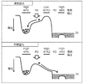
- an image in which the light source is lit is obtained (or a bright image is obtained).
- an image with the light source turned off is obtained (or a dark image is obtained). That is, a phenomenon in which flicker appears in the captured image itself occurs.
- flicker suppression suppressing such imaging failure caused by flicker is referred to as flicker suppression.
- Patent Document 1 in order to expand the dynamic range, at low illuminance, the exposure time is lengthened using high sensitivity pixels, and at high illuminance, the exposure time is shortened using low sensitivity pixels. ing.
- the present disclosure provides a solid-state imaging device and an imaging device that achieve both flicker suppression and dynamic range expansion.
- a solid-state imaging device includes a plurality of high-sensitivity pixels that are arranged in a matrix and photoelectrically convert with a predetermined sensitivity, and are arranged in a matrix in a gap between the plurality of high-sensitivity pixels.
- a plurality of low-sensitivity pixels that perform photoelectric conversion at a sensitivity lower than the sensitivity, a differential signal between the signal from the high-sensitivity pixel and the signal from the low-sensitivity pixel, and the signal of the high-sensitivity pixel is detected by the differential signal
- a signal processing unit that generates a pixel signal by performing correction.
- the solid-state imaging device and the imaging device of the present disclosure it is possible to achieve both flicker suppression and dynamic range expansion.
- FIG. 1 is a block diagram illustrating a configuration example of the solid-state imaging device according to the first embodiment.
- FIG. 2 is a diagram illustrating a circuit example of the pixel circuit according to the first embodiment.
- FIG. 3 is a time chart illustrating an operation example of pixel readout according to the first embodiment.
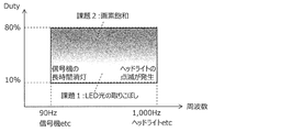
- FIG. 4 is an explanatory diagram of LED flicker.
- FIG. 5 is a time chart illustrating an operation example of pixel readout with gain control according to the first embodiment.
- FIG. 6A is a diagram showing a control voltage and a pixel saturation level of the low sensitivity pixel according to the first embodiment.
- 6B is a diagram showing illuminance / exposure time and charge accumulation level according to Embodiment 1.
- FIG. 7 is a diagram illustrating an arrangement example of high-sensitivity pixels and low-sensitivity pixels according to the first embodiment.
- FIG. 8A is a diagram showing an example of the exposure operation of the high-sensitivity pixel and the low-sensitivity pixel according to Embodiment 1.
- FIG. 8B is a diagram showing an example of the exposure operation and row scanning of the high-sensitivity pixel and the low-sensitivity pixel according to Embodiment 1.
- FIG. 9A is a diagram illustrating a configuration example of a signal processing unit according to Embodiment 1.
- FIG. 9B is a diagram illustrating a configuration example of a correction circuit according to the first embodiment.
- FIG. 9C is an explanatory diagram illustrating an operation example of the signal processing unit of FIG. 9A according to Embodiment 1.
- FIG. 9A is a diagram showing an example of the exposure operation of the high-sensitivity pixel and the low-sensitivity pixel according to Embodiment 1.
- FIG. 8B is a diagram showing an example of the exposure operation and row
- FIG. 10 is a diagram illustrating an example of characteristics of the high-sensitivity pixel and the low-sensitivity pixel with respect to subject illuminance according to the first embodiment.
- FIG. 11 is an explanatory diagram illustrating an example of WDR synthesis in the signal processing unit of FIG. 9A according to the first embodiment.
- FIG. 12A is a diagram illustrating another configuration example of the signal processing unit according to Embodiment 1.
- 12B is an explanatory diagram illustrating an operation example of the signal processing unit of FIG. 12A according to Embodiment 1.
- FIG. 13 is an explanatory diagram illustrating an example of WDR synthesis in the signal processing unit in FIG. 12A according to the first embodiment.
- FIG. 14 is a diagram illustrating a circuit example of the pixel circuit according to the second embodiment.
- FIG. 15 is a time chart illustrating an operation example of pixel readout with gain control according to the second embodiment.
- FIG. 16A is a diagram showing a control voltage and a pixel saturation level of the low sensitivity pixel according to the second embodiment.
- FIG. 16B is a diagram showing the illuminance / exposure time and the charge accumulation level according to the second embodiment.
- FIG. 17 is a diagram illustrating an arrangement example of high-sensitivity pixels and low-sensitivity pixels according to the second embodiment.
- FIG. 18A is a diagram showing an example of exposure times of high-sensitivity pixels and low-sensitivity pixels according to Embodiment 2.
- FIG. 18B is a diagram showing an example of exposure times and row scanning of high-sensitivity pixels and low-sensitivity pixels according to Embodiment 2.
- FIG. 19A is a diagram illustrating a configuration example of a signal processing unit according to Embodiment 2.
- FIG. 19B is an explanatory diagram illustrating an operation example of the signal processing unit of FIG. 19A according to the second embodiment.
- FIG. 20 is a diagram illustrating characteristics of a high-sensitivity pixel and a low-sensitivity pixel with respect to subject illuminance according to the second embodiment.
- FIG. 21 is an explanatory diagram illustrating an example of WDR synthesis in the signal processing unit of FIG. 19A according to the second embodiment.
- FIG. 22A is a time chart showing normal exposure and intermediate exposure according to Embodiment 3.
- FIG. 22B is an explanatory diagram showing an operation example of normal exposure and intermediate exposure according to Embodiment 3.
- FIG. 23A is a diagram showing an example of exposure times of high-sensitivity pixels and low-sensitivity pixels according to Embodiment 3.
- FIG. 23B is a diagram showing an example of exposure times and row scanning of high-sensitivity pixels and low-sensitivity pixels according to Embodiment 3.
- FIG. 24A is a diagram showing another example of the exposure time of the high-sensitivity pixel and the low-sensitivity pixel according to Embodiment 3.
- FIG. 24B is a diagram showing another example of exposure times and row scanning of high-sensitivity pixels and low-sensitivity pixels according to Embodiment 3.
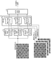
- FIG. 25A is a block diagram illustrating a configuration example of an imaging apparatus according to Embodiment 4.
- FIG. 25B is a block diagram illustrating another configuration example of the imaging apparatus according to Embodiment 4.
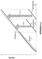
- FIG. 26A is a diagram illustrating an example in which the imaging apparatus according to Embodiment 4 is mounted on an automobile.
- FIG. 26B is a diagram illustrating an example of an imaging range in the mounting example of FIG. 26
- FIG. 4 is an explanatory diagram of LED flicker.
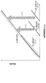
- the horizontal axis of the figure shows the flicker frequency, that is, the frequency with one cycle of turning on and off the LED.
- the vertical axis indicates the flicker duty, that is, the lighting ratio in the cycle of lighting and extinguishing.
- the flicker frequency of a traffic light is about 90 Hz
- the flicker frequency of a car headlight is about 1000 Hz.
- a plurality of pixels having different sensitivities are provided, and a correct image is output by processing output signals of the plurality of pixels.
- the first problem is to miss LED light (light emission that repeatedly turns on and off, pulsed light) (Problem 1).
- the cause is the discrepancy between the exposure timing by the rolling shutter and the LED lighting timing, particularly when the exposure time is short at the bright time (Cause 1).
- This can be solved by lengthening the low-sensitivity pixel exposure time with a high saturation / sensitivity ratio (for example, one vertical scanning period) (Countermeasure 1).
- the second problem is pixel saturation (task 2).
- the cause is that when the duty of the LED flicker is large or the exposure time is long, the pixel reaches a saturation level and the white balance is lost (Cause 2). For this, a plurality of pixels having different saturation / sensitivity ratios are mounted to make it difficult for pixel saturation to occur, and the dynamic range of low-sensitivity pixels is expanded (measure 2).
- the low-sensitivity pixel that captures the LED light may be equipped with a plurality of pixels having different saturation / sensitivity ratios (Countermeasure 2) from the constant exposure (Countermeasure 1) with respect to the above problems 1 and 2.
- the exposure time and gain parameters of the low-sensitivity pixels that image this discontinuous LED light may be set independently of the exposure time and gain parameters of the high-sensitivity pixels that image continuous light.
- both dynamic range expansion and flicker suppression are compatible with high-sensitivity pixels and low-sensitivity pixels with different sensitivities.
- High-sensitivity pixels and low-sensitivity pixels are exposed in parallel, and the exposure time of low-sensitivity pixels is high. This can be realized by generating a one-pixel signal by correcting the signal of the high-sensitivity pixel with the signal of the low-sensitivity pixel that is longer than the exposure time of the pixel.
- the specification of this low sensitivity pixel is that a photogate structure is used to increase the saturation level, and an ND filter (gray filter) is used to decrease the sensitivity, and the saturation / sensitivity ratio is increased. May be.
- the gain in the pixel is increased, and the noise generated in the pixel amplification transistor or the analog circuit is adjusted according to the amount of received light.
- the voltage (pixel signal) may be increased.
- a high-quality image with a high SN Simulal to Noise ratio
- the dynamic range is expanded and a long exposure time is possible.
- the gradation corresponding to the subject is accurately reproduced to enable output of an image without overexposure, and flicker can be suppressed.
- the present inventors have used a low sensitivity pixel with a high saturation / sensitivity ratio as a technique for expanding the dynamic range and suppressing flicker, thereby improving the image quality at low illumination and expanding the dynamic range at high illumination and flicker.
- the inventors have come up with a solid-state imaging device that achieves both suppression.
- FIG. 1 is a block diagram illustrating a configuration example of a solid-state imaging device 1 according to an embodiment.
- the solid-state imaging device 1 shown in FIG. 1 includes a pixel array unit 10, a horizontal scanning circuit 12, a vertical scanning circuit 14, a plurality of vertical signal lines 19, a timing control unit 20, a column processing unit 26, a reference signal generation unit 27, and an output circuit. 28 and a signal processing unit 70.
- the solid-state imaging device 1 also includes an MCLK terminal that receives an input of a master clock signal from the outside, a DATA terminal for transmitting / receiving commands or data to / from the outside, a D1 terminal for transmitting video data to the outside, and the like. In addition to this, terminals for supplying a power supply voltage and a ground voltage are provided.
- the pixel array unit 10 has a plurality of pixel circuits 3 arranged in a matrix.
- the plurality of pixel circuits 3 are arranged in n rows and m columns in FIG.
- Each pixel circuit 3 includes at least a pair of high sensitivity pixels and low sensitivity pixels. That is, each pixel circuit 3 includes at least one high-sensitivity pixel that performs photoelectric conversion with a predetermined sensitivity and at least one low-sensitivity pixel that performs photoelectric conversion with a sensitivity lower than the predetermined sensitivity.
- the horizontal scanning circuit 12 scans the memory 256 in the plurality of column AD circuits 25 in order, and outputs the AD-converted pixel signal to the horizontal signal line 18. This scanning may be the same as the arrangement order of the column AD circuits 25.
- the vertical scanning circuit 14 scans a horizontal scanning line group (also referred to as a row control line group) 15 provided for each row of the pixel circuit 3 in the pixel array unit 10 in units of rows. As a result, the vertical scanning circuit 14 selects the pixel circuits 3 in units of rows, and simultaneously outputs pixel signals from the pixel circuits 3 belonging to the selected row to m vertical signal lines 19.
- the horizontal scanning line groups 15 are provided in the same number as the rows of the pixel circuits 3. In FIG. 1, n horizontal scanning line groups 15 (V1, V2,..., Vn in FIG. 1) are provided.
- Each of the horizontal scanning line groups 15 includes a reset control line ⁇ RS, readout control lines ⁇ TR1, ⁇ TR2, a gain control line ⁇ GC, and a selection control line ⁇ SEL.
- the vertical signal line 19 is provided for each column of the pixel circuits 3 in the pixel array unit 10, and propagates pixel signals from the pixel circuits 3 belonging to the selected row to the column AD circuit 25.
- the plurality of vertical signal lines 19 are composed of m vertical signal lines H1 to Hm in FIG. In FIG. 1, the plurality of ADC input lines are composed of m ADC input lines ADIN1 to ADINm.
- the timing control unit 20 controls the entire solid-state imaging device 1 by generating various control signal groups.
- the various control signal groups include control signal groups CN1, CN2, CN4, CN5, CN8, and a counter clock signal CK0.
- the timing control unit 20 receives the master clock MCLK via a terminal, generates various internal clocks, and controls the horizontal scanning circuit 12, the vertical scanning circuit 14, and the like.
- the column processing unit 26 includes a column AD circuit 25 provided for each column.
- Each column AD circuit 25 AD converts the pixel signal from the vertical signal line 19.
- Each column AD circuit 25 includes a voltage comparator 252, a counter unit 254, and a memory 256.
- the voltage comparator 252 compares the analog pixel signal from the vertical signal line 19 with the reference signal RAMP including a ramp waveform (that is, a triangular wave) generated by the reference signal generation unit 27. For example, the former is more than the latter. When it becomes larger, the output signal indicating the comparison result is inverted.
- a ramp waveform that is, a triangular wave
- the counter unit 254 counts the time from the start of the change of the triangular wave in the reference signal RAMP until the output signal of the voltage comparator 252 is inverted. Since the time until inversion is determined according to the value of the analog pixel signal, the count value becomes the value of the digitized pixel signal.
- the memory 256 holds a count value of the counter unit 254, that is, a digital pixel signal.
- the reference signal generation unit 27 generates a reference signal RAMP including a triangular wave, and outputs the reference signal RAMP to the plus input terminal of the voltage comparator 252 in each column AD circuit 25.
- the output circuit 28 outputs a digital pixel signal to the video data terminal D1.
- the signal processing unit 70 includes a correction unit 75 and a WDR synthesis circuit 76, detects a difference signal between the signal from the high sensitivity pixel and the signal from the low sensitivity pixel, and corrects the signal of the high sensitivity pixel by the difference signal. As a result, a pixel signal is generated. Thereby, the signal processing unit 70 achieves both expansion of the dynamic range and flicker suppression.
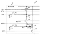
- FIG. 2 is a diagram illustrating a circuit example of the pixel circuit 3 according to the first embodiment.
- the pixel circuit 3 in the figure includes a pair of high-sensitivity pixels PD and low-sensitivity pixels K, a floating diffusion layer FD, a first transfer transistor TR1, a second transfer transistor TR2, a reset transistor RS, and a gain control transistor GC. And an amplification transistor SF and a selection transistor SEL.
- the high-sensitivity pixel PD is a photoelectric conversion element such as a photodiode, and performs photoelectric conversion with a predetermined sensitivity, that is, generates a charge corresponding to the amount of received light.
- the low sensitivity pixel K is a photoelectric conversion element such as a photodiode, and performs photoelectric conversion with a sensitivity lower than a predetermined sensitivity.
- the light receiving area of the low sensitivity pixel K is smaller than the light receiving area of the high sensitivity pixel PD.
- the low sensitivity pixel K is provided with a control electrode PG that covers a part of the low sensitivity pixel K.
- the control electrode PG controls the potential of the surface of the corresponding low-sensitivity pixel K in accordance with the voltage applied to the control electrode PG (control voltage ⁇ PG in the figure). Thereby, the control electrode PG can increase or decrease the saturation level of the low sensitivity pixel K.
- the floating diffusion layer FD holds a signal charge (for example, electrons) transferred from the high sensitivity pixel PD or the low sensitivity pixel K, converts the held signal charge into a voltage, and supplies the converted voltage to the gate of the amplification transistor SF. To do.
- the substantial capacitance of the floating diffusion layer FD is not only the capacitance of the floating diffusion layer FD itself but also the gate capacitance Cfd1 of the amplification transistor SF, the gate-drain capacitance Cp1 of the amplification transistor SF, and the gain control transistor GC. Including the stray capacitance Cfd2 of the drain wiring of the gain control transistor GC.
- the first transfer transistor TR1 is a switch transistor that is turned on and off in response to the read control signal ⁇ TR1.
- the first transfer transistor TR1 transfers the signal charge photoelectrically converted by the high sensitivity pixel PD to the floating diffusion layer FD when the read control signal ⁇ TR1 is at a high level (in other words, reads).
- the second transfer transistor TR2 is a switch transistor that is turned on and off in response to the read control signal ⁇ TR2.
- the second transfer transistor TR2 transfers the signal charge photoelectrically converted by the low sensitivity pixel K to the floating diffusion layer FD via the gain control transistor GC when the read control signal ⁇ TR2 is at the high level (in other words, reads). ).
- the reset transistor RS is a switch transistor that is turned on and off in response to the reset control signal ⁇ RS.
- the reset transistor RS sets the power supply voltage applied to the drain as the reset level to the floating diffusion layer FD via the gain control transistor GC. That is, the reset transistor RS resets the floating diffusion layer FD to the reset level when the reset control signal ⁇ RS is at the high level.
- the gain control transistor GC electrically disconnects or connects the second transfer transistor TR2 and the floating diffusion layer FD according to the gain control signal ⁇ GC. Thereby, the conversion gain for converting the signal charge in the floating diffusion layer FD into a voltage is changed. That is, in the transfer of signal charges from the high-sensitivity pixel PD to the floating diffusion layer FD, the conversion gain of the floating diffusion layer FD is further increased if the gain control transistor GC is turned off. Further, in the transfer of signal charges from the low sensitivity pixel K to the floating diffusion layer FD, the conversion gain of the floating diffusion layer FD is lowered by turning on the gain control transistor GC.
- the amplifying transistor SF forms a source follower together with the load current source 30 connected to the vertical signal line 19 and outputs the gate voltage, that is, the voltage of the floating diffusion layer FD to the vertical signal line 19 as an analog pixel signal.
- the selection transistor SEL is a switch transistor that is turned on and off in response to the selection control signal ⁇ SEL.
- the selection transistor SEL electrically connects the source of the amplification transistor SF and the vertical signal line 19 when the selection control signal ⁇ SEL is at a high level.
- the pixel circuit 3 shown in FIG. 2 shows an example of a 2-pixel 1-cell structure.
- “2 pixels” means that there are two high-sensitivity pixels PD and low-sensitivity pixels K, that is, two photoelectric conversion elements such as photodiodes.
- “1 cell” corresponds to a circuit unit including the floating diffusion layer FD, the reset transistor RS, the amplification transistor SF, and the selection transistor SEL shared by the “2 pixels”.
- FIG. 3 is a time chart showing an example of a signal reading operation accompanying one exposure operation of the solid-state imaging device 1 according to the embodiment.
- the solid-state imaging device 1 performs a plurality of exposure operations with different exposure times within one vertical scanning period for high-sensitivity pixels.
- the solid-state imaging device 1 performs one exposure operation within one vertical scanning period for the low-sensitivity pixels.
- the reference signal RAMP becomes a triangular wave in each of the down-count period (t10 to t14) and the up-count period (t20 to t24) in FIG.
- the down-count period is a period for AD converting the level of the reset component Vrst in the analog pixel signal output from the amplification transistor SF.
- the counter unit 254 counts down the time from the start of the down count period (start of change of the triangular wave) until the output of the voltage comparator 252 is inverted. This count value is the AD conversion result itself of the reset component Vrst of the analog pixel signal.
- the up-count period is a period for AD converting the level of the data component (signal component Vsig + reset component Vrst) of the analog pixel signal output from the amplification transistor SF.
- the time from the start of the up-count period (start of change of the triangular wave) until the output of the voltage comparator 252 is inverted is up-counted by the counter unit.
- This up-count converts the data component (Vsig + Vrst) of the analog pixel signal into a digital value. Since this up-count uses a down-count value indicating the reset component Vrst as an initial value, the count value at the end of the up-count period is a CDS (Correlated Double Sampling) that subtracts the reset component from the data component.
- CDS Correlated Double Sampling
- the column AD circuit 25 eliminates variations such as clock skew and counter delay of each column that cause an error, and extracts only the true signal component Vsig, that is, performs digital CDS.
- FIG. 5 is a time chart showing an operation example of pixel readout with gain control according to the first embodiment.
- the gain for converting the signal charge in the floating diffusion layer FD into a voltage can be switched between a high gain and a low gain according to the on / off of the gain control transistor GC.
- FIG. 5A shows a signal charge read operation from the high-sensitivity pixel PD to the floating diffusion layer FD in a state where the conversion gain of the floating diffusion layer FD is high.
- FIG. 5B shows a signal charge read operation from the low-sensitivity pixel K to the floating diffusion layer FD when the conversion gain of the floating diffusion layer FD is low.
- the floating diffusion layer FD is reset by the positive pulse of the reset control signal ⁇ RS, and the signal charge is transferred from the high sensitivity pixel PD by the positive pulse of the readout control signal ⁇ TR1.
- the read control signal ⁇ TR1 is at a high level
- the gain control signal ⁇ GC is at a low level
- the gain control transistor GC is off. That is, the capacitance of the floating diffusion layer FD is mainly Cfd1, and the FD conversion gain is increased.
- the floating diffusion layer FD is reset by the positive pulse of the reset control signal ⁇ RS, and the signal charge is transferred from the low-sensitivity pixel K by the positive pulse of the read control signal ⁇ TR2.
- the read control signal ⁇ TR2 is at a high level
- the gain control signal ⁇ GC is at a high level
- the gain control transistor GC is on. That is, the capacitance of the floating diffusion layer FD is mainly Cfd1 + Cfd2, and the FD conversion gain is lowered.
- the gain control transistor GC increases the conversion gain of the floating diffusion layer FD if the gain control signal ⁇ GC is at a low level during reading. Conversely, if it is at a high level during reading, it becomes low.
- the low-sensitivity pixel K can change the signal charge amount that can be accumulated near the surface of the low-sensitivity pixel K, and thus the saturation level, by the control voltage ⁇ PG.
- the control voltage ⁇ PG is at a high level during the exposure time, and more signal charges are accumulated.
- the control voltage ⁇ PG is at a low level, and the signal charge is discharged.
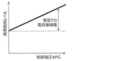
- FIG. 6A is a diagram showing a control voltage ⁇ PG and a pixel saturation level of the low sensitivity pixel K according to the first embodiment.
- the horizontal axis represents the control voltage ⁇ PG
- the vertical axis represents the pixel saturation level.
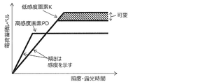
- FIG. 6B is a diagram showing the illuminance / exposure time and the charge accumulation level according to the first embodiment.
- the horizontal axis of the figure shows the product of illuminance and exposure time, illuminance for a fixed time, or exposure time at a fixed illuminance.
- the vertical axis represents the charge accumulation level.
- the charge accumulation region of the low-sensitivity pixel K is composed of a region formed deep like a conventional photodiode without the control electrode PG and a region newly formed near the surface by the control electrode PG.
- the control voltage ⁇ PG is a low voltage
- charges are mainly accumulated in a deep region
- the control voltage ⁇ PG is high
- charges are also accumulated in a shallow region near the surface.
- the saturation level of the low-sensitivity pixel K is variable as shown in FIGS. 6A and 6B in accordance with the potential of the control voltage ⁇ PG.
- the sensitivity of the low-sensitivity pixel K is obtained by stacking an ND (Neutral Density) filter, for example, a gray filter, on an on-chip filter (R, Gr, B, Gb), and adjusting the thickness and stacking region of the gray filter. Can be adjusted. Further, as an alternative to the ND filter, metal shading can be performed to adjust the opening area and adjust the sensitivity.
- the shutter and readout use rolling drive. As shown in FIG. 6B, the saturation level of the low sensitivity pixel K is higher than that of the high sensitivity pixel PD, and the sensitivity of the low sensitivity pixel K is lower than that of the high sensitivity pixel PD.
- the saturation level and the sensitivity level can be adjusted separately, the slope of the charge accumulation level and the saturation level can be set to appropriate values with respect to the product of illuminance and exposure time. As a result, the saturation / sensitivity ratio can be adjusted, and the dynamic range of the pixel can be arbitrarily adjusted.
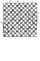
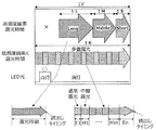
- FIG. 7 is a diagram illustrating an arrangement example of high-sensitivity pixels and low-sensitivity pixels according to the first embodiment.
- the solid-state imaging device 1 has a plurality of pixel groups G0 arranged in a matrix.
- the pixel group G0 has four high-sensitivity pixels PD arranged in the square area and four low-sensitivity pixels K arranged in the square area.
- R, Gr, B, and Gb in the pixel group G0 in the figure indicate four high-sensitivity pixels PD.
- Four K in the pixel group G0 in the figure indicate four low-sensitivity pixels K.
- the solid-state imaging device 1 according to the present embodiment has one high-sensitivity pixel PD and one low-sensitivity pixel K as a pair.
- the four high-sensitivity pixels PD (R, Gr, B, and Gb in the figure) and the four low-sensitivity pixels K corresponding to each of them are in a basic Bayer array.
- the sensitivity can be reduced by stacking a gray filter on the on-chip filter (R, Gr, B, Gb) to attenuate incident light.
- the saturation level of the low sensitivity pixel K is larger than that of the high sensitivity pixel PD, and the sensitivity of the low sensitivity pixel K can be made smaller than that of the high sensitivity pixel PD.
- the dynamic range for the lighting signal of the low-sensitivity pixel can be increased.
- a signal from a relatively low illuminance traffic light in the same frame is increased. It can receive light up to illuminance headlights.
- the pixel circuit 3 of two pixels and one cell shown in FIG. 2 corresponds to GS1 to GS4 in FIG.
- the solid-state imaging device 1 generates a plurality of high-sensitivity frames by performing a plurality of exposure operations with different exposure times within one vertical scanning period with respect to the high-sensitivity pixel PD.
- a low-sensitivity frame is generated by performing one exposure operation within one thrust operation period.
- the signal processing unit 70 corrects each signal of the plurality of high sensitivity frames with a signal from the low sensitivity pixel K, and synthesizes the plurality of corrected high sensitivity frames.
- FIG. 8A is a diagram showing an example of the exposure operation of the high-sensitivity pixel and the low-sensitivity pixel according to Embodiment 1.
- FIG. 8B is a diagram showing an example of the exposure operation and row scanning of the high sensitivity pixel and the low sensitivity pixel according to the first embodiment.
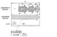
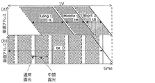
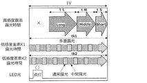
- the solid-state imaging device 1 performs the first exposure operation (Long), the second exposure for exposing the high-sensitivity pixel PD for the first exposure time (tL) within one vertical scanning period 1V.
- the first exposure operation Long
- the second exposure for exposing the exposure time (tM)
- a third exposure operation (Short) that exposes for the third exposure time tS
- the first high-sensitivity frame (L) and the second high-sensitivity frame (M) and a third high sensitivity frame (S) are generated.
- the solid-state imaging device 1 performs an exposure operation in which the low-sensitivity pixel K is exposed for an exposure period (tK) corresponding to one vertical scanning period within one vertical scanning period 1V, and a low-sensitivity frame (K) is obtained. Generate. In each of the first exposure operation, the second exposure operation, the third exposure operation, and the exposure operation for the low-sensitivity pixel K, the readout operation shown in FIG. 3 is performed.
- the solid-state imaging device 1 exposes the high-sensitivity pixel PD three times with different exposure times (tL, tM, tS) in a time-sharing manner in order to expand the dynamic range.
- exposure is performed with an exposure time tK longer than that of the high sensitivity pixel PD.
- the LED light in FIG. 8A cannot be exposed by the exposure operation (Long, Middle, Short) of the high-sensitivity pixel PD ( ⁇ mark), but can be exposed by the low-sensitivity pixel K ( ⁇ mark). It can be seen that flicker suppression can be achieved by correcting the pixel PD signal with the low-sensitivity pixel K signal.
- FIG. 8B shows an output sequence of the high-sensitivity pixel PD and the low-sensitivity pixel K as rolling shutter driving by row scanning.
- Each exposure time of the high sensitivity pixel PD and the low sensitivity pixel K can be arbitrarily set.
- the exposure time tK of the low-sensitivity pixel K substantially the same as one vertical scanning period, it is possible to ensure that the lighting signal is emitted when imaging a light emitting source (pulse light emitting source, LED light source) that periodically turns on and off. It can be captured by the low sensitivity pixel K.
- a light emitting source pulse light emitting source, LED light source
- the low-sensitivity pixel photodiode K which has a higher saturation / sensitivity ratio than the high-sensitivity pixel PD, has low to high illuminance external light (pulse light, LED light, LD light). ). That is, it is possible to continuously receive light on the time axis for the problem of the lighting signal, and to widely receive light by the low sensitivity pixel K for the problem of the dynamic range.
- the high saturation / sensitivity ratio has the following meaning. That is, the low sensitivity pixel K has a higher saturation level and / or a lower sensitivity than the high sensitivity pixel PD.
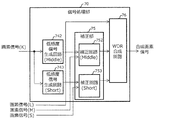
- FIG. 9A is a diagram illustrating a configuration example of the signal processing unit 70 according to the first embodiment.
- the signal processing unit 70 includes a low sensitivity signal generation circuit 742, a low sensitivity signal generation circuit 743, a correction unit 75, and a WDR synthesis circuit 76.
- the correction unit 75 includes a correction circuit 752 and a correction circuit 753.
- FIG. 9B is a diagram illustrating a configuration example of the correction circuit 752 according to the first embodiment.
- FIG. 9C is an explanatory diagram illustrating an operation example of the signal processing unit 70 of FIG. 9A according to Embodiment 1. Note that the correction circuit 753 may have the same configuration as that in FIG. 9B.
- the low-sensitivity signal generation circuit 742 generates a new second low-sensitivity frame signal by multiplying the pixel signal (K) of the low-sensitivity pixel K by the second coefficient.
- the second coefficient is a coefficient for scaling the pixel signal (K) of the low sensitivity pixel K to the pixel signal (M) of the second high sensitivity frame.
- the second coefficient is determined according to the exposure time tK, the second exposure time tM, the gain and sensitivity of the high sensitivity pixel PD, and the gain and sensitivity of the low sensitivity pixel K.
- the low sensitivity signal generation circuit 743 generates a new third low sensitivity frame signal by multiplying the pixel signal (K) of the low sensitivity pixel K by the third coefficient.
- the third coefficient is a coefficient for scaling the pixel signal (K) of the low sensitivity pixel K to the pixel signal (S) of the third high sensitivity frame.
- the third coefficient is determined according to the exposure time tK, the second exposure time tM, the gain and sensitivity of the high sensitivity pixel PD, and the gain and sensitivity of the low sensitivity pixel K.
- the correction circuit 752 detects a difference signal indicating a difference between the pixel signal (M) from the second high sensitivity frame and the signal from the second low sensitivity frame generated by the low sensitivity signal generation circuit 742, and outputs a second signal.
- a second correction signal is generated by correcting the pixel signal (M) from the high-sensitivity frame with the difference signal.
- the correction circuit 752 includes a difference detection circuit 757 and an addition circuit 758.
- the difference detection circuit 757 detects a difference signal between the pixel signal (M) of the second high sensitivity frame and the signal of the second low sensitivity frame.
- the addition circuit 758 adds the difference signal from the difference detection circuit 757 to the pixel signal (M) of the second high sensitivity frame and outputs the addition result as a second correction signal.
- the correction circuit 753 detects the difference signal between the pixel signal (S) from the third high sensitivity frame and the signal from the third low sensitivity frame, and the pixel signal (S) from the third high sensitivity frame is detected as the difference signal. To generate a third correction signal.
- the correction circuit 753 may be the same as that in FIG. 9B, detects the difference between the pixel signal (S) of the second high sensitivity frame and the signal of the third low sensitivity frame, and adds the difference to the pixel signal (S). The addition result is output as a third correction signal.
- the WDR synthesis circuit 76 generates a synthesized pixel signal by synthesizing the pixel signal (L) from the first high-sensitivity frame, the second correction signal from the correction circuit 752, and the third correction signal from the correction circuit 753.
- the low-sensitivity signal generation circuit 742 and the low-sensitivity signal generation circuit 743 generate the dynamic range for the wide dynamic range function (WDR function) from the pixel signal (K) of the low-sensitivity pixel K.
- WDR function wide dynamic range function
- the high-sensitivity pixel PD by performing the first exposure operation, the second exposure operation, and the third exposure operation with different exposure times, the first high-sensitivity pixel frame (L) and the second high-sensitivity frame (M ) And the third high sensitivity frame (S).
- the correcting unit 75 corrects the second high sensitivity frame (M) and the third high sensitivity frame (S) with the second low sensitivity frame and the third low sensitivity frame, and corrects the corrected second high sensitivity frame (M). ) And the corrected third high-sensitivity frame (S).
- the WDR synthesis circuit 76 corrects the pixel signal (L) of the first high-sensitivity frame that has not been corrected, the corrected pixel signal (M) of the corrected second high-sensitivity frame, and the corrected third high-sensitivity frame.
- the pixel signal (S) is synthesized. By this synthesis, a wide dynamic range function (WDR function) is realized, that is, the dynamic range is expanded.
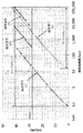
- FIG. 10 is a diagram illustrating an example of photoelectric conversion characteristics of the high-sensitivity pixel and the low-sensitivity pixel with respect to the object illuminance according to the first embodiment.
- FIG. 10 shows the SN of the image with respect to the subject illuminance by connecting the output signals of the pixel signal (L), the pixel signal (M), and the pixel signal (S) from the high-sensitivity pixel PD in FIG. 9C.
- the SN of the image with respect to the subject illuminance is shown with respect to the output signal of the pixel signal (K).
- a wide dynamic range can be secured in a state where the SN at each exposure boundary (Knee point) is satisfied.
- each exposure time tL: tM: tS may be about 256: 16: 1.
- the low sensitivity pixel K may be exposed in parallel with the high sensitivity pixel PD, and the exposure time may be tK> tL + tM + tS.
- FIG. 11 is an explanatory diagram illustrating a synthesis example in the signal processing unit of FIG. 9A according to the first embodiment.
- the WDR synthesis circuit 76 includes a pixel signal (L) of the first high sensitivity frame, a second correction signal (that is, a correction pixel signal (M)) from the low sensitivity signal generation circuit 742, a low
- the third correction signal that is, the correction pixel signal (S)) from the sensitivity signal generation circuit 743 is input and synthesized.
- L pixel signal
- M correction pixel signal
- S correction pixel signal
- the WDR synthesis circuit 76 includes a pixel signal (L), a signal obtained by multiplying the correction pixel signal (M) by the synthesis coefficient G1, and a signal obtained by multiplying the correction pixel signal (S) by the synthesis coefficient G2. Are combined to generate a combined pixel signal.
- the solid-state imaging device 1 includes a plurality of high-sensitivity pixels that are arranged in a matrix and photoelectrically convert with a predetermined sensitivity, and are arranged in a matrix in the plurality of high-sensitivity pixel gaps. Detecting a plurality of low-sensitivity pixels that perform photoelectric conversion at a sensitivity lower than a predetermined sensitivity, a difference signal between a signal from the high-sensitivity pixel and a signal from the low-sensitivity pixel, and converting the signal of the high-sensitivity pixel to the difference And a signal processing unit 70 that generates a pixel signal by correcting the signal.
- the high-sensitivity pixel is exposed in parallel with the low-sensitivity pixel, and the exposure time of the low-sensitivity pixel is longer than the exposure time of the high-sensitivity pixel and shorter than one vertical synchronization period, It may be longer than a predetermined flicker cycle.
- the predetermined flicker cycle may be the longest flashing cycle among general LED light source flashing cycles such as an LED traffic signal.
- the signal processing unit 70 may add the difference signal to the signal of the high sensitivity pixel as the correction.
- the configuration of the correction circuit is simplified and suitable for speeding up.
- the solid-state imaging device 1 generates a plurality of high-sensitivity frames by performing a plurality of exposure operations with different exposure times within one vertical scanning period with respect to the high-sensitivity pixels, and the signal processing unit 70 may correct the signals of each of the plurality of high-sensitivity frames with signals from the low-sensitivity pixels, and synthesize the plurality of high-sensitivity frames after correction.
- the dynamic range can be easily expanded by a plurality of signals having different exposure times within one vertical period from the high sensitivity pixel. Further, flicker can be suppressed by correction.
- the solid-state imaging device 1 has a first exposure operation in which exposure is performed for a first exposure time, a second exposure operation in which exposure is performed for a second exposure time, and a third in one vertical scanning period for the high-sensitivity pixels.
- a first high-sensitivity frame, a second high-sensitivity frame, and a third high-sensitivity frame are generated by performing a third exposure operation in which exposure is performed for the exposure time.
- the first exposure time is longer than the second exposure time
- the second exposure time The time is longer than the third exposure time
- the signal processing unit 70 adds the second coefficient and the third coefficient corresponding to the second exposure time and the third exposure time to the frame composed of the signal of the low sensitivity pixel.
- a second low-sensitivity frame and a third low-sensitivity frame are generated, a difference signal between the signal from the second high-sensitivity frame and the signal from the second low-sensitivity frame is detected, and the first 2 High sensitivity
- a second correction signal is generated by correcting the signal from the frame with the difference signal, a difference signal between the signal from the third high-sensitivity frame and the signal from the third low-sensitivity frame is detected;
- a signal from three high-sensitivity frames is corrected by the difference signal to generate a third correction signal, and the signal from the first high-sensitivity frame, the second correction signal, and the third correction signal are combined to generate the pixel.
- a signal may be generated.
- the solid-state imaging device 1 includes a plurality of pixel circuits 3 arranged in a matrix, and each of the plurality of pixel circuits 3 includes at least one high-sensitivity pixel and a floating diffusion that holds a signal charge.
- a first transfer transistor provided corresponding to each of the layer FD, the at least one high-sensitivity pixel, and transferring a signal charge of the corresponding high-sensitivity pixel to the floating diffusion layer; and at least one low-sensitivity pixel;
- a second transfer transistor provided corresponding to each of the at least one low-sensitivity pixel and transferring a signal charge of the corresponding low-sensitivity pixel to the floating diffusion layer, the second transfer transistor, and the floating diffusion layer;
- a transistor GC that electrically disconnects or connects the transistors.
- the solid-state imaging device 1 further includes a control electrode PG that is provided for each of the plurality of low-sensitivity pixels and covers a part of the corresponding low-sensitivity pixel, and the control electrode PG May control the surface potential of the corresponding low-sensitivity pixel according to the voltage applied to the control electrode PG.
- FIG. 12A is a diagram illustrating another configuration example of the signal processing unit 70 according to Embodiment 1.
- FIG. 12B is an explanatory diagram showing an operation example of the signal processing unit 70 of FIG. 12A.
- FIG. 12A is mainly different from FIG. 9A in that a low-sensitivity signal generation circuit 741 and a correction circuit 751 are added.
- a low-sensitivity signal generation circuit 741 and a correction circuit 751 are added.
- the low sensitivity signal generation circuit 741 generates a first low sensitivity frame from the pixel signal (K) of the low sensitivity pixel K. Specifically, the signal processing unit 70 adds the first exposure time (tL), the second exposure time (tM), and the third exposure time (tS) to the frame configured by the pixel signal (K) of the low sensitivity pixel K. ) To generate a first low sensitivity frame, a second low sensitivity frame, and a third low sensitivity frame, respectively.
- the first coefficient is a coefficient for scaling the pixel signal (K) of the low sensitivity pixel K to the pixel signal (L) of the first high sensitivity frame. For example, the first coefficient is determined according to the exposure time tK, the first exposure time tL, the gain and sensitivity of the high sensitivity pixel PD, and the gain and sensitivity of the low sensitivity pixel K.
- the correction circuit 751 has the same internal configuration as the correction circuit 752, and the difference between the pixel signal (L) from the first high sensitivity frame and the signal from the first low sensitivity frame generated by the low sensitivity signal generation circuit 741. Is detected, and the pixel signal (L) from the first high-sensitivity frame is corrected by the difference signal to generate a first correction signal.
- the WDR synthesis circuit 76 generates a synthesized pixel signal by synthesizing the first correction signal from the correction circuit 751, the second correction signal from the correction circuit 752, and the third correction signal from the correction circuit 753.
- the low-sensitivity signal generation circuits 741, 742, and 743 of FIG. 12A use the first low-sensitivity frame for the wide dynamic range function (WDR function) from the pixel signal (K) of the low-sensitivity pixel K. 3 frames of the third low sensitivity frame are generated.
- WDR function wide dynamic range function
- the correction unit 75 converts the first high sensitivity frame (L), the second high sensitivity frame (M), and the third high sensitivity frame (S) into the first low sensitivity frame, the second low sensitivity frame, and the third low sensitivity frame.
- the corrected first high-sensitivity frame (L), the corrected second high-sensitivity frame (M), and the corrected third high-sensitivity frame (S) are generated.
- the WDR synthesis circuit 76 corrects the corrected pixel signal (L) of the corrected first high sensitivity frame, the corrected pixel signal (M) of the corrected second high sensitivity frame, and the corrected pixel of the corrected third high sensitivity frame.
- the signal (S) is synthesized.
- FIG. 13 is an explanatory diagram illustrating a synthesis example in the signal processing unit 70 of FIG. 12A according to the second embodiment.
- the WDR synthesis circuit 76 has a first correction signal (that is, a correction pixel signal (L) from the low-sensitivity signal generation circuit 741 and a second correction signal (that is, a low-sensitivity signal generation circuit 742).
- the corrected pixel signal (M)) and the third correction signal (that is, the corrected pixel signal (S)) from the low-sensitivity signal generation circuit 743 are inputted and synthesized, and in the synthesis example of FIG.
- a corrected pixel signal (L), a signal obtained by multiplying the corrected pixel signal (M) by the synthesis coefficient G1, and a signal obtained by multiplying the corrected pixel signal (S) by the synthesis coefficient G2 are added together.
- a pixel signal is generated.
- the composite pixel signal in FIG. 13 uses the correction pixel signal (L) instead of the pixel signal (L), as compared with FIG.
- the solid-state imaging device 1 exposes the high-sensitivity pixels for the first exposure time within one vertical scanning period.
- the first high sensitivity frame, the second high sensitivity frame, and the third high sensitivity frame are generated by performing the exposure operation, the second exposure operation that exposes only for the second exposure time, and the third exposure operation that exposes for the third exposure time.
- the first exposure time is longer than the second exposure time
- the second exposure time is longer than the third exposure time
- the signal processing unit 70 applies the first exposure to the frame composed of the signals of the low-sensitivity pixels.
- the first low sensitivity frame, the second low sensitivity frame, and the third low sensitivity frame are generated by multiplying the first coefficient, the second coefficient, and the third coefficient according to the third exposure time from the time, respectively, High sensitivity frame And a signal from the first low-sensitivity frame is detected, the signal from the first high-sensitivity frame is corrected by the difference signal to generate a first correction signal, and the second Detecting a difference signal between the signal from the high sensitivity frame and the signal from the second low sensitivity frame, and correcting the signal from the second high sensitivity frame by the difference signal to generate a second correction signal; A difference signal between the signal from the third high sensitivity frame and the signal from the third low sensitivity frame is detected, and the signal from the third high sensitivity frame is corrected by the difference signal to obtain a third correction signal. And generating the pixel signal by combining the first correction signal, the second correction signal, and the third correction signal.
- Embodiment 2 Next, the solid-state imaging device 1 according to Embodiment 2 will be described.
- a configuration example of the solid-state imaging device 1 including two types of low-sensitivity pixels K1 and K2 instead of the low-sensitivity pixel K will be described.
- FIG. 14 is a diagram illustrating a circuit example of the pixel circuit 3 according to the second embodiment.
- the pixel circuit 3 has a four-pixel one-cell structure, high-sensitivity pixels PD1 and PD2, low-sensitivity pixels K1 and K2, readout transistors TR11 and TR12 corresponding to the high-sensitivity pixels PD1 and PD2, and low-sensitivity pixels K1 and K2.
- read transistors TR21 and TR22 a reset transistor RS, a gain control transistor GC, a floating diffusion layer FD, an amplification transistor SF, and a selection transistor SEL.
- the high-sensitivity pixels PD1 and PD2 and the low-sensitivity pixels K1 and K2 are light-receiving elements that perform photoelectric conversion, and generate charges according to the amount of light received.
- the sensitivity of the high sensitivity pixel PD1 and the high sensitivity pixel PD2 is the same.
- the sensitivity of the low sensitivity pixel K1 and the low sensitivity pixel K2 is different.
- the high sensitivity pixel PD1 and the low sensitivity pixel K1 are a pair, and the high sensitivity pixel PD2 and the low sensitivity pixel K2 are a pair.
- the floating diffusion layer FD temporarily holds charges read from the high-sensitivity pixels PD1 and PD2 and the low-sensitivity pixels K1 and K2 by the read transistors TR11, TR12, TR21, and TR22, respectively.
- FIG. 15 is a time chart showing an example of pixel readout operation with gain control.
- the gain for converting the signal charge in the floating diffusion layer FD into a voltage can be switched between a high gain and a low gain according to the on / off of the gain control transistor GC.
- FIG. 15A shows an operation of reading signal charges from the high-sensitivity pixel PD1 or PD2 to the floating diffusion layer FD in a state where the conversion gain of the floating diffusion layer FD is high.
- FIG. 15B shows an operation of reading signal charges from the low-sensitivity pixel K1 or K2 to the floating diffusion layer FD when the conversion gain of the floating diffusion layer FD is low.
- the floating diffusion layer FD is reset by the positive pulse of the reset control signal ⁇ RS, and the signal charge is transferred from the high sensitivity pixel PD1 or PD2 by the positive pulse of the read control signal ⁇ TR11 or ⁇ TR12.
- the gain control signal ⁇ GC is at a low level, and the gain control transistor GC is off. That is, the capacitance of the floating diffusion layer FD is mainly Cfd1, and the FD conversion gain is increased.
- the floating diffusion layer FD is reset by the positive pulse of the reset control signal ⁇ RS, and the signal charge is transferred from the low-sensitivity pixel K1 or K2 by the positive pulse of the read control signal ⁇ TR21 or ⁇ TR22.
- the gain control signal ⁇ GC is at a high level, and the gain control transistor GC is on. That is, the capacitance of the floating diffusion layer FD is mainly Cfd1 + Cfd2, and the FD conversion gain is lowered.
- the gain control transistor GC increases the conversion gain of the floating diffusion layer FD if the gain control signal ⁇ GC is at a low level during reading. Conversely, if it is at a high level during reading, it becomes low.
- the low-sensitivity pixels K1 and K2 can change the amount of signal charge that can be accumulated near the surface of the low-sensitivity pixel K, and thus the saturation level, by the control voltage ⁇ PG.
- the control voltage ⁇ PG is at a high level during the exposure time, and more signal charges are accumulated.
- the control voltage ⁇ PG is at a low level, and the signal charge is discharged.
- the pixel circuit 3 may have a multi-pixel 1-cell structure other than the 4-pixel 1-cell structure.
- the unit pixel of the multi-pixel 1-cell structure has, for example, a plurality of photoelectric conversion elements, and any or all of the floating diffusion layer FD, the reset transistor RS, the amplification transistor SF, and the selection transistor SEL are shared within the unit cell. It may be a structure.
- FIG. 16A is a diagram showing control voltages and pixel saturation levels of the low-sensitivity pixels K1 and K2 according to the second embodiment.
- FIG. 16B is a diagram showing the illuminance / exposure time and the charge accumulation level according to the second embodiment.
- FIG. 16A shows that the saturation levels of the low-sensitivity pixels K1 and K2 are variable by the control voltages ⁇ PG1 and ⁇ PG2, similarly to FIG. 6A. Since the control electrode PG of the low sensitivity pixel K has such characteristics, as shown in FIG. 16B, (saturation / sensitivity ratio of the low sensitivity pixel K1) ⁇ (saturation / sensitivity of the low sensitivity pixel K2). Ratio), (control voltage ⁇ PG1 ⁇ control voltage ⁇ PG2).
- the sensitivity of the low-sensitivity pixels K1 and K2 is determined by stacking an ND filter, for example, a gray filter, on the on-chip filter (R, Gr, B, Gb), and adjusting the thickness and stacking area of the gray filter. Sensitivity can be adjusted. Further, as an alternative to the ND filter, metal shading can be performed to adjust the opening area and adjust the sensitivity.
- the shutter and readout use rolling drive.
- the saturation level and the sensitivity level in FIG. 16B can be adjusted separately, the slope of the charge accumulation level and the saturation level can be set to appropriate values for the product of illuminance and exposure time. As a result, the saturation / sensitivity ratio can be adjusted, and the dynamic range of the pixel can be arbitrarily adjusted.
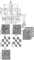
- FIG. 17 is a diagram illustrating an arrangement example of the high sensitivity pixels PD1 and PD2 and the low sensitivity pixels K1 and K2 according to the second embodiment.
- the solid-state imaging device 1 has a plurality of first pixel groups G1 and a plurality of second pixel groups G2.
- the first pixel group G1 has four high-sensitivity pixels PD1 arranged in the square area and four low-sensitivity pixels K1 arranged in the square area.
- the second pixel group G2 includes four high-sensitivity pixels PD2 arranged in the square area and four low-sensitivity pixels K2 arranged in the square area.
- the first pixel group G1 and the second pixel group G2 are alternately arranged in the row direction and the column direction.
- each of the first pixel groups G1 and G2 basically includes four high-sensitivity pixels and four low-sensitivity pixels.
- the four high sensitivity pixels PD1 or PD2 are indicated by (R, Gr, B, Gb).
- the low sensitivity pixels having a small saturation / sensitivity ratio are collectively referred to as K1, and the large pixels are collectively referred to as K2.
- the first pixel group G1 includes four high-sensitivity pixels (R, Gr, B, and Gb) and four low-sensitivity pixels K1 corresponding to the high-sensitivity pixels (R, Gr, B, and Gb).
- the second pixel group G2 includes four high-sensitivity pixels (R, Gr, B, Gb) and four low-sensitivity pixels K2 corresponding thereto.
- the four high-sensitivity pixels PD1 or PD2 in the first pixel group G1 or the second pixel group are in a Bayer array.
- the four low-sensitivity pixels K1 are also in a Bayer array.
- the four low-sensitivity pixels K2 are also in a Bayer array.
- the low sensitivity pixel K1 and the low sensitivity pixel K2 have different saturation / sensitivity ratios.
- the saturation / sensitivity ratio of the low sensitivity pixel K1 is smaller than that of the low sensitivity pixel K2.
- the dynamic range for the lighting signals of the low-sensitivity pixels K1 and K2 can be increased.
- a light source that repeatedly turns on and off (pulse light source, LED light source) has a relatively low illuminance in the same frame. It can receive signals from traffic lights to high-intensity headlights.
- the configuration example of the pixel circuit 3 illustrated in FIG. 14 corresponds to the pixel groups GS5 and GS6 in FIG.
- FIG. 18A is a diagram showing an example of exposure times of the high-sensitivity pixels PD1 and PD2 and the low-sensitivity pixels K1 and K2 according to Embodiment 2.
- FIG. 18B is a diagram showing an example of exposure times and row scanning of the high sensitivity pixels PD1 and PD2 and the low sensitivity pixels according to the second embodiment.
- the high sensitivity pixel PD1 has the same sensitivity and the same saturation level as the high sensitivity pixel PD2.
- the high-sensitivity pixels PD1 and PD2 perform a first exposure operation (Long) in which exposure is performed for a first exposure time (tL) within one vertical scanning period 1V,
- a second exposure operation Moddle
- a third exposure operation (Short) for exposure for the third exposure time tS
- the first high-sensitivity frame (L), the second high A sensitivity frame (M) and a third high sensitivity frame (S) are generated.
- the solid-state imaging device 1 performs an exposure operation in which the low-sensitivity pixel K1 is exposed for an exposure period (tK1) corresponding to one vertical scanning period within one vertical scanning period 1V, and the low-sensitivity frame (K1) is displayed. Generate. Similarly, the solid-state imaging device 1 performs an exposure operation in which the low-sensitivity pixel K2 is exposed for an exposure period (tK2) corresponding to one vertical scanning period within one vertical scanning period 1V, and the low-sensitivity frame (K2). Is generated.
- high-sensitivity pixels are exposed three times with different exposure times (tL, tM, tS) in a time-sharing manner in order to expand the dynamic range.
- the low sensitivity pixels K1 and K2 are exposed in parallel with a longer exposure time than the high sensitivity pixels. That is, tK1> tL + tM + tS and tK2> tL + tM + tS.
- the LED light in the figure cannot be exposed during the exposure period (Long, Middle, Short) of the high-sensitivity pixel ( ⁇ mark), but can be exposed at the low-sensitivity pixels K1 and K2 ( ⁇ mark). It can be seen that flicker suppression can be achieved by correcting the pixel signal with the low-sensitivity pixel signal.
- FIG. 18B shows an output sequence of high-sensitivity pixels and low-sensitivity pixels as rolling shutter drive, and each exposure time can be arbitrarily set for both K1 and K2.
- the exposure times tK1 and tK2 of the low-sensitivity pixels K1 and K2 substantially the same as one vertical scanning period, when the light source that repeatedly turns on and off (pulse light source, LED light source) is received, the lighting signal is surely received. It can be captured with low-sensitivity pixels.
- the saturation / sensitivity ratio of the low sensitivity pixel K1 is smaller than that of the low sensitivity pixel K2.
- the low-sensitivity pixel K1 saturation / sensitivity ratio: small
- the low-sensitivity pixel K2 saturation / sensitivity ratio: large
- the low-sensitivity pixel K2 saturation / sensitivity ratio: large
- FIG. 19A is a diagram illustrating a configuration example of the signal processing unit 70 according to the second embodiment.
- FIG. 19B is an explanatory diagram illustrating an operation example of the signal processing unit 70 of FIG. 19A according to the second embodiment.
- the correction circuits 751 and 753 may have the same configuration as that in FIG. 9B.
- FIG. 19A differs from FIG. 12A mainly in that a dividing circuit 721, an interpolation circuit 731 and an interpolation circuit 732 are added, and the low sensitivity signal generation circuits 741 to 743 perform different operations.
- a dividing circuit 721 an interpolation circuit 731 and an interpolation circuit 732 are added, and the low sensitivity signal generation circuits 741 to 743 perform different operations.
- different points will be mainly described.
- the dividing circuit 721 includes a low-sensitivity frame in which the pixel signal (K1) of the low-sensitivity pixel K1 and the pixel signal (K2) from the low-sensitivity pixel K2 are mixed, and is composed of the pixel signal (K1).
- the frame is divided into a low sensitivity frame (K1) and a low sensitivity frame (K2) made up of pixel signals (K2).
- Interpolation circuit 731 generates an interpolated low sensitivity frame (K1) by interpolating the missing pixel signal in the low sensitivity frame (K1).
- an interpolation composed of a plurality of pixel signals (K1) obtained from a plurality of low-sensitivity pixels K1 and a plurality of interpolation signals (P1) obtained by interpolation using the plurality of pixel signals (K1).
- a low sensitivity frame (K1) is generated.
- the interpolation signal P1 is generated by performing weighted interpolation according to the position of the center of gravity using at least four surrounding pixel signals (K1).
- Interpolation circuit 732 generates an interpolated low sensitivity frame (K2) by interpolating missing pixel signals in the low sensitivity frame (K2).
- an interpolation composed of a plurality of pixel signals (K2) obtained from a plurality of low-sensitivity pixels K2 and a plurality of interpolation signals (P2) obtained by interpolation using the plurality of pixel signals (K2).
- a low sensitivity frame (K2) is generated.
- the interpolation signal P2 is generated by performing weighted interpolation according to the position of the center of gravity using at least four surrounding pixel signals (K2).
- the low sensitivity signal generation circuit 741 synthesizes the pixel signal (K1 or P1) of the interpolation low sensitivity frame (K1) and the pixel signal (P2 or K2) of the interpolation low sensitivity frame (K2), thereby generating the first high signal.
- a first low sensitivity frame (L) for correcting the sensitivity frame (L) is generated.
- the low-sensitivity signal generation circuit 741 multiplies the pixel signal (K1 or P1) of the interpolation low-sensitivity frame (K1) by the first type first coefficient to obtain the pixel signal (P2) of the interpolation low-sensitivity frame (K2).
- K2 is multiplied by the second type first coefficient.
- the first type first coefficient is a coefficient corresponding to the first exposure time (tL) and the exposure time (tK1) of the low-sensitivity pixel K1, and is the pixel signal (K1 or K1) of the interpolation low-sensitivity frame (K1).
- P1) is a coefficient for scaling the pixel signal (L) of the first high sensitivity frame.
- the first type first coefficient is determined according to the exposure time tK1, the first exposure time tL, the gain and sensitivity of the high sensitivity pixel PD, and the gain and sensitivity of the low sensitivity pixel K1.
- the second type first coefficient is a coefficient corresponding to the first exposure time (tL) and the exposure time (tK2) of the low-sensitivity pixel K2, and is the pixel signal (K2 or P2) is a coefficient for scaling the pixel signal (L) of the first high sensitivity frame.
- the first type first coefficient is determined according to the exposure time tK2, the first exposure time tL, the gain and sensitivity of the high sensitivity pixel PD, and the gain and sensitivity of the low sensitivity pixel K2.
- the low sensitivity signal generation circuit 741 combines the interpolated low sensitivity frame (K1) multiplied by the first type first coefficient and the interpolated low sensitivity frame (K2) multiplied by the second type first coefficient.
- the first low sensitivity frame (L) is generated.
- the low sensitivity signal generation circuit 742 combines the pixel signal (K1 or P1) of the interpolation low sensitivity frame (K1) and the pixel signal (P2 or K2) of the interpolation low sensitivity frame (K2), thereby generating the second high signal.
- a second low sensitivity frame (M) for correcting the sensitivity frame (M) is generated.
- the low-sensitivity signal generation circuit 742 multiplies the pixel signal (K1 or P1) of the interpolated low-sensitivity frame (K1) by the first type second coefficient to obtain the pixel signal (P2) of the interpolated low-sensitivity frame (K2).
- K2 is multiplied by the second type second coefficient.
- the first type second coefficient is a coefficient corresponding to the second exposure time (tM) and the exposure time (tK1) of the low sensitivity pixel K1, and is the pixel signal (K1 or K1) of the interpolation low sensitivity frame (K1).
- P1) is a coefficient for scaling the pixel signal (M) of the second high sensitivity frame.
- the first type second coefficient is determined according to the exposure time tK1, the second exposure time tM, the gain and sensitivity of the high sensitivity pixel PD, and the gain and sensitivity of the low sensitivity pixel K1.
- the second type second coefficient is a coefficient corresponding to the second exposure time (tM) and the exposure time (tK2) of the low-sensitivity pixel K2, and is the pixel signal (K2 or P2) is a coefficient for scaling the pixel signal (M) of the second high sensitivity frame.
- the second type second coefficient is determined according to the exposure time tK2, the second exposure time tM, the gain and sensitivity of the high sensitivity pixel PD, and the gain and sensitivity of the low sensitivity pixel K2.
- the low sensitivity signal generation circuit 742 combines the interpolated low sensitivity frame (K1) multiplied by the first type second coefficient and the interpolated low sensitivity frame (K2) multiplied by the second type second coefficient.
- the second low sensitivity frame (M) is generated.
- the low sensitivity signal generation circuit 743 combines the pixel signal (K1 or P1) of the interpolation low sensitivity frame (K1) and the pixel signal (P2 or K2) of the interpolation low sensitivity frame (K2), thereby generating the third high signal.
- a third low sensitivity frame (S) for correcting the sensitivity frame (S) is generated.
- the low-sensitivity signal generation circuit 742 multiplies the pixel signal (K1 or P1) of the interpolation low-sensitivity frame (K1) by the first type and third coefficient to obtain the pixel signal (P2) of the interpolation low-sensitivity frame (K2).
- K2 is multiplied by the second type third coefficient.
- the first type third coefficient is a coefficient corresponding to the third exposure time (tS) and the exposure time (tK1) of the low sensitivity pixel K1, and is the pixel signal (K1 or K1) of the interpolation low sensitivity frame (K1).
- P1) is a coefficient for scaling the pixel signal (S) of the second high sensitivity frame.
- the first type third coefficient is determined according to the exposure time tK1, the third exposure time tS, the gain and sensitivity of the high sensitivity pixel PD, and the gain and sensitivity of the low sensitivity pixel K1.
- the second type third coefficient is a coefficient corresponding to the third exposure time (tS) and the exposure time (tK2) of the low-sensitivity pixel K2, and is the pixel signal (K2 or the interpolation low-sensitivity frame (K2)).
- P2) is a coefficient for scaling the pixel signal (S) of the third high sensitivity frame.
- the second type third coefficient is determined according to the exposure time tK2, the third exposure time tS, the gain and sensitivity of the high sensitivity pixel PD, and the gain and sensitivity of the low sensitivity pixel K2.
- the low sensitivity signal generation circuit 743 combines the interpolated low sensitivity frame (K1) multiplied by the first type third coefficient and the interpolated low sensitivity frame (K2) multiplied by the second type third coefficient.
- the third low sensitivity frame (S) is generated.
- the correction unit 75 and the WDR synthesis circuit 76 are the same as those in FIG. 12A.
- FIG. 20 is a diagram illustrating the characteristics of the high-sensitivity pixel and the low-sensitivity pixel with respect to subject illuminance according to the second embodiment.
- FIG. 21 is an explanatory diagram showing an example of WDR synthesis in the signal processing unit 70 of FIG. 19A according to the second embodiment. 20 and 21 are used for the pixel signal (K1) and the pixel signal (K2) instead of the pixel signal (K), as compared with FIGS. 10 and 11, the expansion of the dynamic range is more effective. It has become.
- the exposure times of the low-sensitivity pixels K1 and K2 are tK1> tL + tM + tS and tK2> tL + tM + tS. It may be about 1/90 Hz).
- saturation / sensitivity ratio of the low-sensitivity pixels K1, K2 “saturation / sensitivity ratio of the low-sensitivity pixel K1: saturation / sensitivity ratio of the low-sensitivity pixel K2” is, for example, 1:20, and the maximum subject illuminance ( Even if it receives 100,000 lux of the illuminance of sunlight, it may not be saturated.
- the dynamic range (DR) of the high-sensitivity pixel is calculated as follows.
- the DR of the low sensitivity pixels K1 and K2 is set to draw an SN curve from 100,000 lux.
- the solid-state imaging device adjusts the control voltage ⁇ PG of the control electrode PG so that the low-sensitivity pixel is not saturated and the saturation level is not too low in the signal processing of the low-sensitivity pixel.
- AE automatic exposure control
- white balance can be performed.
- the center of gravity is corrected so that the center of gravity of the pixel does not shift.
- control electrode PG has a problem of dark current because it accumulates charges near the surface, and the image quality (S / N) is poor, and in particular, it may be unacceptable as a low illuminance image quality that emphasizes S / N.
- the low-sensitivity pixel having the control electrode PG is used for correcting the high-sensitivity pixel signal for flicker suppression, and thus has no problem that the S / N deteriorates.
- the low-sensitivity pixels K, K1, and K2 have an example of having a control electrode PG having a photogate structure as a saturation level adjusting unit. However, if a desired saturation / sensitivity ratio can be adjusted only by sensitivity adjustment, It does not have to have a structure.
- the plurality of low-sensitivity pixels include the plurality of first low-sensitivity pixels K1 and the plurality of second low-sensitivity pixels K2, and the first low-sensitivity pixels K1. At least one of the signal saturation level and sensitivity of the sensitivity pixel K1 is different from that of the second low sensitivity pixel K2.
- the solid-state imaging device 1 includes a plurality of first pixel groups G1 and a plurality of second pixel groups G2, and the first pixel group G1 includes the four high-sensitivity pixels arranged in a square region. And the four first low-sensitivity pixels arranged in the square area, and the second pixel group G2 is arranged in the square area and the four high-sensitivity pixels arranged in the square area.
- the four second low-sensitivity pixels may be provided, and the first pixel group G1 and the second pixel group G2 may be alternately arranged in the row direction and the column direction.
- the signal processing unit 70 includes a plurality of first pixel signals obtained from the plurality of first pixel signals obtained from the plurality of first low-sensitivity pixels and a plurality of first interpolations obtained by interpolation using the plurality of first pixel signals.
- a second interpolation frame composed of the second interpolation signal is generated, and a difference signal between the signal from the high-sensitivity pixel and the signal obtained by combining the first interpolation frame and the second interpolation frame
- the pixel signal may be generated by correcting the signal of the high-sensitivity pixel with the difference signal.
- the solid-state imaging device 1 has a first exposure operation in which exposure is performed for a first exposure time, a second exposure operation in which exposure is performed for a second exposure time, and a third in one vertical scanning period for the high-sensitivity pixels.
- a first high-sensitivity frame, a second high-sensitivity frame, and a third high-sensitivity frame are generated by performing a third exposure operation in which exposure is performed for the exposure time.
- the first exposure time is longer than the second exposure time
- the second exposure time The time is longer than the third exposure time
- the signal processing unit 70 converts the first interpolation frame and the second interpolation frame from the first coefficient to the third coefficient corresponding to the third exposure time.
- a signal from the first high sensitivity frame and a signal from the first low sensitivity frame are generated.
- Difference with And a signal from the first high sensitivity frame is corrected by the difference signal to generate a first correction signal, and a signal from the second high sensitivity frame, a signal from the second low sensitivity frame, and And a second correction signal is generated by correcting the signal from the second high-sensitivity frame with the difference signal, and the signal from the third high-sensitivity frame and the third low-sensitivity frame are detected.
- a signal from the third high-sensitivity frame is corrected by the difference signal to generate a third correction signal, and the first correction signal, the second correction signal, and the third correction signal are detected.
- the pixel signal may be generated by combining signals.
- FIG. 22A is a time chart showing normal exposure and intermediate exposure according to the third embodiment.
- FIG. 22B is an explanatory diagram showing an operation example of normal exposure and intermediate exposure according to Embodiment 3.
- the sensitivity of the low-sensitivity pixel K is such that the accumulated charge is varied by adjusting the duty of the pulse of the control voltage ⁇ PG and transfer voltage ⁇ TR of the photodiode described above and repeatedly controlling normal exposure and intermediate exposure (charge discharge).
- the magnitude relationship of sensitivity is K1 if the normal exposure time of K1> the normal exposure time of K2. Sensitivity> K2, and K1 saturation / sensitivity ratio ⁇ K2 saturation / sensitivity ratio.
- the saturation level can be adjusted by the voltage level of ⁇ PG, and the sensitivity level can be adjusted by distributing the normal exposure time and the intermediate exposure time.
- the dynamic range by arbitrarily setting the saturation / sensitivity ratio can be determined arbitrarily.
- the sensitivity of the low-sensitivity pixel K at the time of multiple exposure can be expressed by the following equation.
- Multi-exposure sensitivity (sensitivity 1 ⁇ normal exposure time + sensitivity 2 ⁇ intermediate exposure time) / 1V
- Sensitivity 1 is the sensitivity of normal exposure per 1V.
- Sensitivity 2 is the sensitivity of intermediate exposure per 1V.
- the normal exposure and the intermediate exposure are performed simultaneously for all rows. This is because the rolling shutter drive complicates the design of the address decoding unit of the vertical scanning circuit 14.
- FIG. 23A is a diagram showing an example of exposure times of high-sensitivity pixels and low-sensitivity pixels according to Embodiment 3.
- FIG. 23B is a diagram showing an example of exposure times and row scanning of high-sensitivity pixels and low-sensitivity pixels according to Embodiment 3.
- the solid-state imaging device 1 exposes three times with different exposure times (tL, tM, tS) in a time-sharing manner in order to expand the dynamic range of high-sensitivity pixels.
- the low sensitivity pixel K is subjected to multiple exposure in parallel with an exposure time tK longer than that of the high sensitivity pixel. Multiple exposure is, for example, repetition of normal exposure and intermediate exposure.
- FIG. 23B shows a high-sensitivity pixel output sequence as a rolling shutter drive, and each exposure time can be arbitrarily set.
- the sensitivity of the low-sensitivity pixel K can be set according to the above formula according to the ratio of the sum of the normal exposure times E1 to En and the sum of the intermediate exposure times M1 to Mm.
- the sensitivity can be widely adjusted by the multiple exposure of the low-sensitivity pixel K to the problem of the dynamic range.
- the ratio of the exposure time and the intermediate exposure time of the photodiode K of the low sensitivity pixel can be adjusted.
- 1H exposure time and 3H intermediate exposure time, 1H exposure time and 7H intermediate exposure time, 1H exposure time and 15H intermediate exposure time, 1H exposure time and 31H intermediate exposure time can be set.
- the signal readout drive and the intermediate exposure drive are performed simultaneously, the signal readout drive is designed to have priority.
- the solid-state imaging device 1 includes a plurality of pixel circuits 3 arranged in a matrix, and each of the plurality of pixel circuits 3 includes at least one.
- the high-sensitivity pixels, the floating diffusion layer FD that holds signal charges, and the at least one high-sensitivity pixel are provided to transfer the signal charges of the corresponding high-sensitivity pixels to the floating diffusion layer.
- a second transfer is provided corresponding to each of the first transfer transistor, at least one of the low-sensitivity pixels, and the at least one of the low-sensitivity pixels, and transfers the signal charge of the corresponding low-sensitivity pixel to the floating diffusion layer.
- the solid-state imaging device 1 repeats a normal exposure operation and an intermediate exposure operation within one vertical scanning period for the low-sensitivity pixel, and the normal exposure operation Then, the gate electrode of the second transfer transistor is at a low level, and in the intermediate exposure operation, the gate electrode of the second transfer transistor is at a high level or a middle level, and switching from the normal exposure operation to the intermediate exposure operation is performed. Are performed simultaneously for all the lines, and switching from the intermediate exposure operation to the normal exposure operation is performed for all the lines simultaneously.
- the sensitivity can be widely adjusted by the multiple exposure of the low sensitivity pixel K.
- Embodiment 4 an imaging apparatus according to Embodiment 4 will be described with reference to the drawings.
- the imaging device provided in the present embodiment includes one or more solid-state imaging devices 1 according to Embodiments 1 to 3 described above. Details will be described below.
- FIG. 25A is a block diagram illustrating a configuration example of an imaging apparatus according to the fifth embodiment.
- the imaging apparatus shown in the figure includes a CIS (CMOS Image Sensor) 91, an ISP (Image Signal Processor) 92, and a monitor 93, and is, for example, a digital camera or a smartphone camera.
- CIS CMOS Image Sensor
- ISP Image Signal Processor
- CIS 91 is the solid-state imaging device 1 shown in each embodiment.
- the ISP 92 receives the image signal from the CIS 91 and performs image processing such as image enlargement, reduction, compression encoding, and decoding.
- the monitor 93 is a monitor for user confirmation at the time of imaging.
- the CIS 91 and the ISP 92 may be one-chip SoC (System on Chip) 90 or another chip.
- SoC System on Chip
- the signal processing unit 70 may be provided in the CIS 91 or may be provided in the CIS 92.
- a part of the signal processing unit 70 may be realized by software instead of a circuit.
- FIG. 25B is a block diagram illustrating another configuration example of the imaging apparatus according to Embodiment 5.
- the image pickup apparatus shown in FIG. 1 includes a CIS (CMOS Image Sensor) 91, an ISP (Image Signal Processor) 92, a sensor 94, a sensor ECU (Electronic Control Unit) 95, a warning unit 96, and a control unit 97. This is a camera system to be installed.
- CIS CMOS Image Sensor
- ISP Image Signal Processor
- CIS 91 and ISP 92 are the same as those in FIG. 25A.
- the sensor 94 is, for example, a radar sensor for ranging and a lidar (Light Detection and Ranging) sensor for measuring distance.
- a radar sensor for ranging
- a lidar (Light Detection and Ranging) sensor for measuring distance.
- the sensor ECU 95 controls the warning unit 96 and the control unit 97 that have received signals from the ISP 92 and the sensor 94.
- the warning unit 96 is, for example, various status display lights or warning lights in an instrument panel of a car.
- the control unit 97 controls, for example, an actuator that moves an automobile steering, a brake, or the like.
- 25B corresponds to a sensing system such as a view system, ADAS (Advanced Driver Assistance System) or automatic driving, and is connected to a monitor in the view system, and a sensor ECU in the sensing system. Warning or control (steering, braking, etc.) may be performed via ADAS (Advanced Driver Assistance System) or automatic driving.
- ADAS Advanced Driver Assistance System
- Warning or control may be performed via
- FIG. 26A is a diagram illustrating an example in which the imaging apparatus according to Embodiment 5 is mounted on the automobile M1.
- FIG. 26B is a diagram illustrating an example of an imaging range in the mounting example of FIG. 26A according to the fifth embodiment.
- the imaging device of FIG. 25A is attached to each of a plurality of attachment locations C1 to C9.
- the attachment location C1 is a front portion of the automobile M1.
- the attachment location C2 is a left side portion of the vehicle body of the automobile M1.
- the attachment location C3 is a right side portion of the vehicle body of the automobile M1.
- the attachment location C4 is a left door mirror.
- the attachment location C5 is a right door mirror.
- the attachment location C6 is a room mirror.
- the attachment location C7 is a rear center portion of the automobile M1.
- the attachment location C8 is a rear left portion of the automobile M1.
- the attachment location C9 is a rear right side portion of the automobile M1.
- the imaging ranges S1 to S9 shown in FIG. 26B correspond to the imaging cameras at the attachment points C1 to C9.
- the imaging device as a view camera or a sensing camera can operate the front, surround, side, rear, and intelligent rear of the transportation device (vehicle, automobile) according to the target range of imaging. Can be in the mounting position.
- the imaging apparatus includes the solid-state imaging apparatus 1 described above, and is any one of a view system, an ADAS (advanced driving assistance system) sensing system, and an automatic driving sensing system.
- ADAS advanced driving assistance system
- the imaging device may be mounted on one or more of the front, left side, right side, and rear mirror of the transport device.
- the solid-state imaging device of the present disclosure and the imaging device using the solid-state imaging device have been described based on the above-described embodiment.
- the solid-state imaging device of the present disclosure and the imaging device using the solid-state imaging device are limited to the above-described embodiment. Is not to be done.
- the solid-state imaging device of the present disclosure, and various devices incorporating the imaging device using the same are also included in the present invention.
- the present disclosure can be used for a solid-state imaging device and an imaging device.
Landscapes
- Engineering & Computer Science (AREA)
- Multimedia (AREA)
- Signal Processing (AREA)
- Power Engineering (AREA)
- Physics & Mathematics (AREA)
- Computer Hardware Design (AREA)
- General Physics & Mathematics (AREA)
- Condensed Matter Physics & Semiconductors (AREA)
- Electromagnetism (AREA)
- Microelectronics & Electronic Packaging (AREA)
- Health & Medical Sciences (AREA)
- Biomedical Technology (AREA)
- General Health & Medical Sciences (AREA)
- Life Sciences & Earth Sciences (AREA)
- Sustainable Development (AREA)
- Sustainable Energy (AREA)
- Transforming Light Signals Into Electric Signals (AREA)
- Studio Devices (AREA)
Abstract
La présente invention concerne un dispositif d'imagerie à semi-conducteurs (1) qui comprend : une pluralité de pixels à haute sensibilité qui sont agencés dans un réseau et réalisent une conversion photoélectrique à une sensibilité prescrite ; une pluralité de pixels à faible sensibilité qui sont agencés dans un réseau dans des espaces entre la pluralité de pixels à haute sensibilité et réalisent une conversion photoélectrique à une sensibilité inférieure à la sensibilité prescrite ; et une unité de traitement de signal (70) qui détecte un signal différentiel entre un signal provenant des pixels à haute sensibilité et un signal à partir des pixels à faible sensibilité, utilise le signal différentiel afin de corriger le signal à partir des pixels à haute sensibilité, et génère ainsi un signal de pixel.
Priority Applications (4)
| Application Number | Priority Date | Filing Date | Title |
|---|---|---|---|
| EP17878149.8A EP3554065B1 (fr) | 2016-12-08 | 2017-11-30 | Appareil d'imagerie à semi-conducteurs et appareil d'imagerie |
| CN201780074535.5A CN110036630B (zh) | 2016-12-08 | 2017-11-30 | 固体摄像装置以及摄像装置、输送设备的反射镜 |
| JP2018554955A JP7014734B2 (ja) | 2016-12-08 | 2017-11-30 | 固体撮像装置および撮像装置 |
| US16/431,277 US10847556B2 (en) | 2016-12-08 | 2019-06-04 | Solid-state imaging apparatus and imaging apparatus |
Applications Claiming Priority (2)
| Application Number | Priority Date | Filing Date | Title |
|---|---|---|---|
| US201662431603P | 2016-12-08 | 2016-12-08 | |
| US62/431,603 | 2016-12-08 |
Related Child Applications (1)
| Application Number | Title | Priority Date | Filing Date |
|---|---|---|---|
| US16/431,277 Continuation US10847556B2 (en) | 2016-12-08 | 2019-06-04 | Solid-state imaging apparatus and imaging apparatus |
Publications (1)
| Publication Number | Publication Date |
|---|---|
| WO2018105474A1 true WO2018105474A1 (fr) | 2018-06-14 |
Family
ID=62491024
Family Applications (2)
| Application Number | Title | Priority Date | Filing Date |
|---|---|---|---|
| PCT/JP2017/042989 WO2018105475A1 (fr) | 2016-12-08 | 2017-11-30 | Dispositif d'imagerie à semi-conducteurs et dispositif d'imagerie comprenant un dispositif d'imagerie à semi-conducteurs |
| PCT/JP2017/042988 WO2018105474A1 (fr) | 2016-12-08 | 2017-11-30 | Dispositif d'imagerie à semi-conducteurs et dispositif d'imagerie |
Family Applications Before (1)
| Application Number | Title | Priority Date | Filing Date |
|---|---|---|---|
| PCT/JP2017/042989 WO2018105475A1 (fr) | 2016-12-08 | 2017-11-30 | Dispositif d'imagerie à semi-conducteurs et dispositif d'imagerie comprenant un dispositif d'imagerie à semi-conducteurs |
Country Status (5)
| Country | Link |
|---|---|
| US (2) | US10847556B2 (fr) |
| EP (1) | EP3554065B1 (fr) |
| JP (2) | JP7014734B2 (fr) |
| CN (2) | CN110036630B (fr) |
| WO (2) | WO2018105475A1 (fr) |
Cited By (6)
| Publication number | Priority date | Publication date | Assignee | Title |
|---|---|---|---|---|
| CN110943099A (zh) * | 2018-09-25 | 2020-03-31 | 台湾积体电路制造股份有限公司 | 图像传感器器件及其操作方法 |
| WO2020093651A1 (fr) * | 2018-11-09 | 2020-05-14 | 浙江宇视科技有限公司 | Procédé et appareil de détection et de suppression automatiques de franges, dispositif électronique et support de stockage lisible par ordinateur |
| WO2020095544A1 (fr) * | 2018-11-07 | 2020-05-14 | ソニーセミコンダクタソリューションズ株式会社 | Dispositif d'imagerie et appareil électronique |
| WO2020230636A1 (fr) * | 2019-05-10 | 2020-11-19 | ソニーセミコンダクタソリューションズ株式会社 | Dispositif de reconnaissance d'images et procédé de reconnaissance d'images |
| WO2021199807A1 (fr) * | 2020-03-31 | 2021-10-07 | パナソニックIpマネジメント株式会社 | Dispositif d'imagerie et procédé d'imagerie |
| JP2022125060A (ja) * | 2020-07-20 | 2022-08-26 | 株式会社ユピテル | システム及びプログラム等 |
Families Citing this family (16)
| Publication number | Priority date | Publication date | Assignee | Title |
|---|---|---|---|---|
| JP7014734B2 (ja) | 2016-12-08 | 2022-02-01 | ヌヴォトンテクノロジージャパン株式会社 | 固体撮像装置および撮像装置 |
| JP6748622B2 (ja) * | 2017-02-16 | 2020-09-02 | ソニーセミコンダクタソリューションズ株式会社 | 撮像システムおよび撮像装置 |
| DE102017118160A1 (de) * | 2017-08-09 | 2019-02-14 | Valeo Schalter Und Sensoren Gmbh | Ermitteln der maximalen Reichweite eines LIDAR-Sensors |
| CN109005346B (zh) * | 2018-08-13 | 2020-04-03 | Oppo广东移动通信有限公司 | 控制方法、装置、电子设备和计算机可读存储介质 |
| US10999549B2 (en) * | 2019-06-20 | 2021-05-04 | Pixart Imaging Incorporation | Image sensor, column parallel ADC circuit and A/D conversion method thereof |
| TWI748460B (zh) * | 2019-06-21 | 2021-12-01 | 大陸商廣州印芯半導體技術有限公司 | 飛時測距裝置及飛時測距方法 |
| US11447063B2 (en) * | 2019-07-18 | 2022-09-20 | GM Global Technology Operations LLC | Steerable scanning and perception system with active illumination |
| US10863106B1 (en) * | 2019-10-21 | 2020-12-08 | GM Global Technology Operations LLC | Systems and methods for LED flickering and banding detection |
| US11196937B2 (en) | 2019-11-25 | 2021-12-07 | Qualcomm Incorporated | High frame rate in high dynamic range processing |
| DE102021113883A1 (de) * | 2020-06-04 | 2021-12-09 | Samsung Electronics Co., Ltd. | Bildsensor, elektronische vorrichtung, und betriebsverfahren eines bildsensors |
| CN111683212B (zh) * | 2020-07-20 | 2021-05-04 | 成都微光集电科技有限公司 | 一种图像传感器及其测试方法 |
| CN112165586A (zh) * | 2020-09-28 | 2021-01-01 | 成都微光集电科技有限公司 | Adc功能安全校验装置和方法、cmos图像传感器、参考像素单元 |
| CN114743226A (zh) * | 2020-12-23 | 2022-07-12 | 京东方科技集团股份有限公司 | 图像采集结构及其驱动方法、显示装置 |
| JP2022100908A (ja) * | 2020-12-24 | 2022-07-06 | ゼタテクノロジーズ株式会社 | 固体撮像装置、固体撮像装置の信号処理方法、および電子機器 |
| KR20230000673A (ko) | 2021-06-25 | 2023-01-03 | 삼성전자주식회사 | 듀얼 컨버전 게인을 이용한 노이즈 감소를 위한 이미지 처리 장치 및 그 동작 방법 |
| US11444630B1 (en) * | 2021-06-30 | 2022-09-13 | Novatek Microelectronics Corp. | Column analog-to-digital converter and local counting method thereof |
Citations (3)
| Publication number | Priority date | Publication date | Assignee | Title |
|---|---|---|---|---|
| JP2007266556A (ja) | 2006-03-30 | 2007-10-11 | Fujifilm Corp | 固体撮像装置 |
| JP2011188148A (ja) * | 2010-03-05 | 2011-09-22 | Toshiba Corp | 固体撮像装置 |
| JP2015231095A (ja) * | 2014-06-04 | 2015-12-21 | キヤノン株式会社 | 撮像装置、その制御方法、および制御プログラム |
Family Cites Families (41)
| Publication number | Priority date | Publication date | Assignee | Title |
|---|---|---|---|---|
| JPH07264488A (ja) * | 1995-02-15 | 1995-10-13 | Olympus Optical Co Ltd | 電子的撮像装置 |
| JP3031606B2 (ja) * | 1995-08-02 | 2000-04-10 | キヤノン株式会社 | 固体撮像装置と画像撮像装置 |
| JP2000083261A (ja) * | 1998-09-04 | 2000-03-21 | Advantest Corp | 画像切出装置及びこれを搭載した画像入力ボード |
| JP3730442B2 (ja) * | 1999-05-14 | 2006-01-05 | 株式会社東芝 | 固体撮像装置 |
| JP2002027196A (ja) * | 2000-07-04 | 2002-01-25 | Ricoh Co Ltd | 画像読取装置及び画像形成装置 |
| JP3962278B2 (ja) * | 2002-05-14 | 2007-08-22 | 富士フイルム株式会社 | ディジタルカメラおよびそのシェーディング補正方法 |
| JP2004112742A (ja) * | 2002-07-25 | 2004-04-08 | Fujitsu Ltd | 画像歪みを抑制したイメージセンサ |
| JP4150599B2 (ja) * | 2003-01-17 | 2008-09-17 | 富士フイルム株式会社 | 露出補正機能付きデジタルカメラ |
| JP4468657B2 (ja) * | 2003-04-28 | 2010-05-26 | オリンパス株式会社 | 撮像素子 |
| US7224388B2 (en) * | 2003-05-08 | 2007-05-29 | Micron Technology, Inc. | Wide dynamic range active pixel with knee response |
| JP4466319B2 (ja) * | 2004-10-25 | 2010-05-26 | パナソニック電工株式会社 | 空間情報の検出装置 |
| JP4654857B2 (ja) * | 2005-09-26 | 2011-03-23 | ソニー株式会社 | Da変換装置、ad変換装置、半導体装置 |
| JP4487944B2 (ja) * | 2006-02-09 | 2010-06-23 | ソニー株式会社 | 固体撮像装置 |
| KR101338353B1 (ko) * | 2007-05-30 | 2013-12-06 | 삼성전자주식회사 | 영상 촬상 장치 및 방법 |
| US7825966B2 (en) * | 2007-06-29 | 2010-11-02 | Omnivision Technologies, Inc. | High dynamic range sensor with blooming drain |
| TWI504256B (zh) * | 2008-04-07 | 2015-10-11 | Sony Corp | 固態成像裝置,其訊號處理方法,及電子設備 |
| JP2009278236A (ja) * | 2008-05-13 | 2009-11-26 | Panasonic Corp | 固体撮像装置 |
| JP5115335B2 (ja) * | 2008-05-27 | 2013-01-09 | ソニー株式会社 | 固体撮像素子及びカメラシステム |
| JP4975700B2 (ja) * | 2008-08-06 | 2012-07-11 | シャープ株式会社 | Dac測定方法および固体撮像装置 |
| ATE543215T1 (de) * | 2009-03-24 | 2012-02-15 | Sony Corp | Festkörper-abbildungsvorrichtung, ansteuerverfahren für festkörper- abbildungsvorrichtung und elektronische vorrichtung |
| JP2011044801A (ja) * | 2009-08-19 | 2011-03-03 | Toshiba Corp | 画像処理装置 |
| JP2011091775A (ja) * | 2009-10-26 | 2011-05-06 | Toshiba Corp | 固体撮像装置 |
| JP2012039299A (ja) * | 2010-08-05 | 2012-02-23 | Toshiba Corp | 固体撮像装置 |
| US8823850B2 (en) | 2010-12-30 | 2014-09-02 | Hynix Semiconductor Inc. | Image processing system with on-chip test mode for column ADCs |
| JP2012222529A (ja) * | 2011-04-06 | 2012-11-12 | Sony Corp | 固体撮像素子および駆動方法、並びに電子機器 |
| JP2013055500A (ja) * | 2011-09-02 | 2013-03-21 | Sony Corp | 固体撮像素子およびカメラシステム |
| JP6000589B2 (ja) * | 2012-03-21 | 2016-09-28 | キヤノン株式会社 | 固体撮像装置 |
| JP5980080B2 (ja) * | 2012-10-02 | 2016-08-31 | キヤノン株式会社 | 光電変換装置、撮像システム、光電変換装置の検査方法および撮像システムの製造方法 |
| JP5813067B2 (ja) * | 2012-12-20 | 2015-11-17 | キヤノン株式会社 | 撮像装置の駆動方法、デジタル信号の補正方法、撮像装置、撮像システムの駆動方法、撮像システム |
| JPWO2015033497A1 (ja) * | 2013-09-06 | 2017-03-02 | パナソニックIpマネジメント株式会社 | 固体撮像装置、撮像装置及びその駆動方法 |
| JP6437450B2 (ja) * | 2013-12-04 | 2018-12-12 | ソニーセミコンダクタソリューションズ株式会社 | 画像処理装置、画像処理方法、電子機器、並びにプログラム |
| JP6408372B2 (ja) | 2014-03-31 | 2018-10-17 | ソニーセミコンダクタソリューションズ株式会社 | 固体撮像装置及びその駆動制御方法、並びに、電子機器 |
| JP6406888B2 (ja) * | 2014-06-17 | 2018-10-17 | キヤノン株式会社 | アナログデジタル変換回路の駆動方法、アナログデジタル変換回路、撮像装置、撮像システム、アナログデジタル変換回路の検査方法 |
| JP6448340B2 (ja) | 2014-12-10 | 2019-01-09 | キヤノン株式会社 | 固体撮像装置、撮像システム及び固体撮像装置の駆動方法 |
| JP6700723B2 (ja) * | 2014-12-17 | 2020-05-27 | キヤノン株式会社 | 撮像装置及び撮像素子の駆動方法 |
| US9467633B2 (en) * | 2015-02-27 | 2016-10-11 | Semiconductor Components Industries, Llc | High dynamic range imaging systems having differential photodiode exposures |
| US10498983B2 (en) * | 2015-03-16 | 2019-12-03 | Sony Corporation | Solid-state imaging device, method for driving solid-state imaging device, and electronic apparatus |
| TWI717450B (zh) * | 2016-02-18 | 2021-02-01 | 日商新力股份有限公司 | 固體攝像裝置、固體攝像裝置之驅動方法、及電子機器 |
| KR102641555B1 (ko) * | 2016-03-31 | 2024-02-28 | 소니그룹주식회사 | 고체 촬상 소자, 고체 촬상 소자의 구동 방법, 및, 전자 기기 |
| JP2017183563A (ja) * | 2016-03-31 | 2017-10-05 | ソニー株式会社 | 撮像装置、駆動方法、および、電子機器 |
| JP7014734B2 (ja) * | 2016-12-08 | 2022-02-01 | ヌヴォトンテクノロジージャパン株式会社 | 固体撮像装置および撮像装置 |
-
2017
- 2017-11-30 JP JP2018554955A patent/JP7014734B2/ja active Active
- 2017-11-30 JP JP2018554956A patent/JP7064444B2/ja active Active
- 2017-11-30 EP EP17878149.8A patent/EP3554065B1/fr active Active
- 2017-11-30 WO PCT/JP2017/042989 patent/WO2018105475A1/fr active Application Filing
- 2017-11-30 WO PCT/JP2017/042988 patent/WO2018105474A1/fr unknown
- 2017-11-30 CN CN201780074535.5A patent/CN110036630B/zh active Active
- 2017-11-30 CN CN201780075076.2A patent/CN110036632B/zh active Active
-
2019
- 2019-06-04 US US16/431,277 patent/US10847556B2/en active Active
- 2019-06-04 US US16/431,302 patent/US10685997B2/en active Active
Patent Citations (3)
| Publication number | Priority date | Publication date | Assignee | Title |
|---|---|---|---|---|
| JP2007266556A (ja) | 2006-03-30 | 2007-10-11 | Fujifilm Corp | 固体撮像装置 |
| JP2011188148A (ja) * | 2010-03-05 | 2011-09-22 | Toshiba Corp | 固体撮像装置 |
| JP2015231095A (ja) * | 2014-06-04 | 2015-12-21 | キヤノン株式会社 | 撮像装置、その制御方法、および制御プログラム |
Non-Patent Citations (1)
| Title |
|---|
| See also references of EP3554065A4 |
Cited By (14)
| Publication number | Priority date | Publication date | Assignee | Title |
|---|---|---|---|---|
| CN110943099A (zh) * | 2018-09-25 | 2020-03-31 | 台湾积体电路制造股份有限公司 | 图像传感器器件及其操作方法 |
| TWI736944B (zh) * | 2018-09-25 | 2021-08-21 | 台灣積體電路製造股份有限公司 | 影像感測元件及操作影像感測元件之方法 |
| US11956553B2 (en) | 2018-09-25 | 2024-04-09 | Taiwan Semiconductor Manufacturing Co., Ltd. | Image sensor for sensing LED light with reduced flickering |
| US11172142B2 (en) | 2018-09-25 | 2021-11-09 | Taiwan Semiconductor Manufacturing Co., Ltd. | Image sensor for sensing LED light with reduced flickering |
| CN110943099B (zh) * | 2018-09-25 | 2022-06-07 | 台湾积体电路制造股份有限公司 | 图像传感器器件及其操作方法 |
| WO2020095544A1 (fr) * | 2018-11-07 | 2020-05-14 | ソニーセミコンダクタソリューションズ株式会社 | Dispositif d'imagerie et appareil électronique |
| US11405568B2 (en) | 2018-11-07 | 2022-08-02 | Sony Semiconductor Solutions Corporation | Imaging apparatus and electronic device |
| JP7362651B2 (ja) | 2018-11-07 | 2023-10-17 | ソニーセミコンダクタソリューションズ株式会社 | 撮像装置及び電子機器 |
| US11689817B2 (en) | 2018-11-09 | 2023-06-27 | Zhejiang Uniview Technologies Co., Ltd. | Method and apparatus for automatically detecting and suppressing fringes, electronic device and computer-readable storage medium |
| WO2020093651A1 (fr) * | 2018-11-09 | 2020-05-14 | 浙江宇视科技有限公司 | Procédé et appareil de détection et de suppression automatiques de franges, dispositif électronique et support de stockage lisible par ordinateur |
| WO2020230636A1 (fr) * | 2019-05-10 | 2020-11-19 | ソニーセミコンダクタソリューションズ株式会社 | Dispositif de reconnaissance d'images et procédé de reconnaissance d'images |
| US11710291B2 (en) | 2019-05-10 | 2023-07-25 | Sony Semiconductor Solutions Corporation | Image recognition device and image recognition method |
| WO2021199807A1 (fr) * | 2020-03-31 | 2021-10-07 | パナソニックIpマネジメント株式会社 | Dispositif d'imagerie et procédé d'imagerie |
| JP2022125060A (ja) * | 2020-07-20 | 2022-08-26 | 株式会社ユピテル | システム及びプログラム等 |
Also Published As
| Publication number | Publication date |
|---|---|
| US20190289238A1 (en) | 2019-09-19 |
| JP7064444B2 (ja) | 2022-05-10 |
| JPWO2018105475A1 (ja) | 2019-10-24 |
| US10847556B2 (en) | 2020-11-24 |
| US10685997B2 (en) | 2020-06-16 |
| CN110036630A (zh) | 2019-07-19 |
| CN110036630B (zh) | 2021-08-20 |
| JPWO2018105474A1 (ja) | 2019-10-24 |
| CN110036632A (zh) | 2019-07-19 |
| EP3554065B1 (fr) | 2021-12-29 |
| US20190288020A1 (en) | 2019-09-19 |
| EP3554065A1 (fr) | 2019-10-16 |
| WO2018105475A1 (fr) | 2018-06-14 |
| JP7014734B2 (ja) | 2022-02-01 |
| CN110036632B (zh) | 2021-07-09 |
| EP3554065A4 (fr) | 2020-01-01 |
Similar Documents
| Publication | Publication Date | Title |
|---|---|---|
| JP7014734B2 (ja) | 固体撮像装置および撮像装置 | |
| US10504949B2 (en) | Solid-state imaging device, method of driving solid-state imaging device, imaging system, and movable object | |
| JP6937736B2 (ja) | 固体撮像装置および撮像装置 | |
| US11336844B2 (en) | Imaging device, imaging system, and movable object | |
| WO2021166584A1 (fr) | Dispositif d'imagerie à semi-conducteur et appareil d'imagerie l'utilisant | |
| JP2015109503A (ja) | イメージセンサおよびイメージセンサの動作方法、撮像装置、電子機器、並びにプログラム | |
| KR101939402B1 (ko) | 고체 촬상 소자 및 구동 방법, 및 전자 기기 | |
| US9930273B2 (en) | Image pickup apparatus, image pickup system, and control method for the image pickup apparatus for controlling transfer switches | |
| JP2011049892A (ja) | 撮像装置 | |
| CN108432238B (zh) | 固体摄像装置、固体摄像装置的驱动方法以及电子设备 | |
| US20220070396A1 (en) | Solid-state imaging apparatus, imaging apparatus, and imaging method | |
| US20220053152A1 (en) | Solid-state imaging apparatus and imaging apparatus including the same | |
| JP7204480B2 (ja) | 撮像装置、撮像システム、移動体及び撮像装置の制御方法 | |
| JP5051994B2 (ja) | 固体撮像装置、固体撮像装置の駆動方法および撮像装置 | |
| US20050264663A1 (en) | Image pickup apparatus and image pickup method | |
| CN108432239B (zh) | 固体摄像装置、固体摄像装置的驱动方法以及电子设备 | |
| US20080074526A1 (en) | Image pickup device and image pickup method | |
| JP2010178197A (ja) | 固体撮像装置の駆動方法、固体撮像装置およびカメラ | |
| JP2006237789A (ja) | 撮像装置 | |
| JP2006352295A (ja) | 固体撮像装置、固体撮像装置の駆動方法および撮像装置 | |
| JP2017055244A (ja) | 固体撮像装置 |
Legal Events
| Date | Code | Title | Description |
|---|---|---|---|
| 121 | Ep: the epo has been informed by wipo that ep was designated in this application |
Ref document number: 17878149 Country of ref document: EP Kind code of ref document: A1 |
|
| ENP | Entry into the national phase |
Ref document number: 2018554955 Country of ref document: JP Kind code of ref document: A |
|
| NENP | Non-entry into the national phase |
Ref country code: DE |
|
| ENP | Entry into the national phase |
Ref document number: 2017878149 Country of ref document: EP Effective date: 20190708 |