WO2018105100A1 - 装着ジョブデータの作成方法および作成装置 - Google Patents
装着ジョブデータの作成方法および作成装置 Download PDFInfo
- Publication number
- WO2018105100A1 WO2018105100A1 PCT/JP2016/086714 JP2016086714W WO2018105100A1 WO 2018105100 A1 WO2018105100 A1 WO 2018105100A1 JP 2016086714 W JP2016086714 W JP 2016086714W WO 2018105100 A1 WO2018105100 A1 WO 2018105100A1
- Authority
- WO
- WIPO (PCT)
- Prior art keywords
- electronic component
- job data
- mounting
- finished product
- substrate
- Prior art date
- Legal status (The legal status is an assumption and is not a legal conclusion. Google has not performed a legal analysis and makes no representation as to the accuracy of the status listed.)
- Ceased
Links
Images



Classifications
-
- H—ELECTRICITY
- H05—ELECTRIC TECHNIQUES NOT OTHERWISE PROVIDED FOR
- H05K—PRINTED CIRCUITS; CASINGS OR CONSTRUCTIONAL DETAILS OF ELECTRIC APPARATUS; MANUFACTURE OF ASSEMBLAGES OF ELECTRICAL COMPONENTS
- H05K13/00—Apparatus or processes specially adapted for manufacturing or adjusting assemblages of electric components
Definitions
- the present invention relates to a method for creating mounting job data used in an electronic component mounting machine in the process of producing a finished product substrate, and an apparatus for creating mounting job data.
- the electronic component placement machine operates based on the placement job data, and is in charge of a placement process for placing the electronic component on the original substrate.
- the mounting job data includes position data values when mounting the electronic component on the original substrate, and component data information including the electronic component type and shape information.
- the mounting job data generally further includes information such as the mounting order of a plurality of electronic components, the type of nozzle tool for sucking and mounting the electronic components, and the component supply position.
- the mounting job data is created based on CAD data obtained by CAD design of the finished product board and performance data of the electronic component mounting machine.
- inspection job data used in an appearance board inspection machine arranged in a subsequent process of the electronic component mounting machine is also created based on the same CAD data and performance data of the appearance board inspection machine.
- Patent Documents 1 to 3 disclose technical examples related to creation of mounting job data and inspection job data.
- the mounting data creation method disclosed in Patent Document 1 reads an original substrate having lands with an image scanner, acquires land data such as the shape, size, and center position of each land from the image data, and searches the component library. Then, mounting data (mounting job data) is created by selecting an electronic component corresponding to the land data. According to this, it is said that mounting data necessary for mounting components can be created easily and in a short time and with high accuracy without individual differences among workers, and contributes to the provision of a high-quality finished product board. .
- the mounting line of Patent Document 2 includes an electronic component mounting machine, a board appearance inspection machine, means for controlling the electronic component mounting machine based on production data (mounting job data), and inspection data (inspection job data). ) And a means for acquiring data necessary for the inspection from the production data and creating the inspection data. According to this, inspection data can be automatically created, and the creation of inspection data can be easily performed.
- Patent Document 3 discloses a processing execution method in a component mounting system including an electronic component mounting machine and a board appearance inspection machine.
- an implementation library consisting of implementation-specific data used only for implementation, inspection-specific data used only for inspection, and common data used for both implementation and inspection is provided. Refer to the implementation library. Execute the mounting process and inspection process. According to this, duplication management of data in the electronic component mounting machine and the board appearance inspection machine can be avoided.
- the mounting job data is created from the image data of the original substrate having the land, but there are times when the mounting job data cannot be determined.
- not all lands are necessarily used, and electronic components may or may not be mounted on specific lands depending on whether options are specified.
- the actual finished board is supplied from the client and CAD data is not provided.
- the present invention has been made in view of the above-described problems of the background art, and when creating mounting job data using a finished product substrate as a sample, a method for creating mounting job data that can reduce the burden on the operator compared to the prior art. And providing a creation apparatus is a problem to be solved.
- the method for creating the mounting job data disclosed in the present specification uses an image image acquisition device to capture a finished product image on which an electronic component is mounted on an original substrate, thereby obtaining finished product image data.
- Product image data is image-processed, and shape information representing the shape and size of the original substrate and the electronic component, and position information of the electronic component represented using a coordinate system set on the original substrate are obtained.
- mounting job data used in the electronic component mounting machine in the process of producing the finished product substrate is created.
- the mounting job data creation device disclosed in this specification uses an image image acquisition device to capture a finished product substrate on which an electronic component is already mounted on an original substrate, thereby obtaining finished product image data.
- An acquisition unit and the processed product image data are image-processed to be expressed using shape information representing at least the shape and size of the original substrate and the electronic component, and a coordinate system set on the original substrate.
- An image processing unit that extracts position information of the electronic component, and data creation that generates mounting job data used in the electronic component mounting machine in the process of producing the finished product substrate based on the extracted shape information and the position information A section.
- the finished product image data is obtained using the finished product substrate as a sample, and the shape information of the original substrate and the electronic component, and the position information of the electronic component are extracted.
- the mounting job data used in the electronic component mounting machine is created. Since all or most of the data creation procedure can be automated, the burden on the operator can be reduced as compared with the conventional procedure.
- the same procedure as the above mounting job data creating method can be executed. Therefore, all or most of the procedure can be automated, and the burden on the operator can be reduced as compared with the conventional method.
- FIG. 1 is a diagram schematically illustrating a board production line 1 that implements the method for creating mounting job data according to the embodiment.
- the board production line 1 includes a solder printing machine 2, a solder printing inspection machine 3, an electronic component mounting machine 4, a board appearance inspection machine 5, a reflow machine 6, and a line management device 7. From the solder printer 2 to the reflow machine 6 are arranged in a line in the order described.
- the solder printer 2 prints paste solder on the original substrate in a predetermined pattern shape.
- the solder printing machine 2 and the solder printing inspection machine 3 are connected by a board transfer device 81.
- the solder printing inspection machine 3 inspects the solder printing state of the conveyed board.
- the solder printing inspection machine 3 and the electronic component mounting machine 4 are connected by a board transfer device 82.
- the electronic component mounting machine 4 mounts an electronic component on the solder of the conveyed board.
- the electronic component mounting machine 4 includes a suction nozzle 41 that sucks and mounts electronic components on a substrate. In order to mount a large number of electronic components accurately and efficiently, the electronic component mounting machine 4 operates based on mounting job data.
- the electronic component mounting machine 4 and the board appearance inspection machine 5 are connected by a board transfer device 83.
- the board appearance inspection machine 5 inspects the appearance state of the electronic components mounted on the conveyed board.
- the board appearance inspection machine 5 includes an image image acquisition device 51 that images the appearance of the board. In order to accurately and efficiently inspect a large number of electronic components, the board appearance inspection machine 5 operates based on inspection job data.
- the substrate visual inspection machine 5 and the reflow machine 6 are connected by a substrate transfer device 84.
- the reflow machine 6 solidifies after re-melting the solder of the board determined to be normal by the board visual inspection machine 5, and stabilizes the connection state. This completes the production of the finished product substrate.
- the line management device 7 is configured using a computer with a built-in CPU and operating with software.
- the line management device 7 includes a display device 71 and an input device 72.
- the line management device 7 is communicatively connected to the solder printing machine 2, the solder printing inspection machine 3, the electronic component mounting machine 4, the board appearance inspection machine 5, and the reflow machine 6 using the communication line 73.
- the line management device 7 is further connected to a component library 75 stored in an external storage device using a communication line 73.
- the component library 75 is also shared by other board production lines. In place of the communication line 73, wireless communication means can be used.
- the configuration of the substrate production line 1 shown in FIG. 1 is an example, and may be a variety of known line configurations, for example, a line configuration including a plurality of electronic component mounting machines.
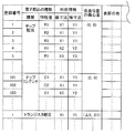
- FIG. 2 is a diagram schematically showing an example of the data structure of the component library 75.
- the component library 75 component data of various types of electronic components is registered in advance.
- the parts library 75 is organized in a list format. That is, the component library 75 has columns such as a registration number, electronic component type, shape information, an adsorption amount eccentricity, and surface brightness or color.
- the electronic component is assigned a registration number for each type, and registration information is set in each column of one line.
- the electronic component with registration number 1 shown in the first row is a chip resistor, and the characteristic value is the resistance value R1.
- the shape information of the electronic component with registration number 1 has a vertical dimension of X1 and a horizontal dimension of Y1.
- the vertical dimension and the horizontal dimension indicate the existence range of the horizontally placed electronic components in two horizontal directions (see Xi and Yi in FIG. 7), and satisfy the relationship of vertical dimension ⁇ horizontal dimension.
- the shape information, the height, weight, etc. of the electronic component can be registered.
- the amount of eccentricity of the suction position of the electronic component with registration number 1 is (0, 0). This indicates that the center position of the upper surface is sucked when the electronic component is sucked by the suction nozzle 41 of the electronic component mounting machine 4.
- the information on the luminance or color of the surface of the electronic component is reflected in the determination value when the board appearance inspection machine 5 distinguishes the outer shape of the electronic component from the ground color of the board.
- registration number 1, registration number 2, and registration number 3 differ only in the characteristic values, and the other information matches each other. Also, the three types of electronic components of registration number 1, registration number 4, and registration number 5 have the same characteristic value and different shape information. Furthermore, although registration number 1 is a chip resistor and registration number 101 is a chip capacitor, the shape information is consistent with each other. As a result, the type of electronic component cannot be specified based only on the shape information.
- the mounting job data is created using the finished product substrate as a sample and using the image image acquisition device 51 of the substrate visual inspection machine 5.
- This creation method is realized mainly by the function of the creation device for creating the mounting job data of the embodiment of the line management device 7.
- the line management device 7 has functions of an image acquisition unit, an image processing unit, an inspection job data creation unit, and a mounting job data creation unit.
- this creation method is performed between operations of the substrate production line 1.
- the present invention is not limited to this, and another computer device connected to the line management device 7 may have the function of a device for creating the mounting job data.
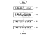
- FIG. 3 is a procedure diagram of a method for creating the mounting job data according to the embodiment.
- the image acquisition unit of the line management device 7 acquires the finished product image data using the image image acquisition device 51 of the board appearance inspection machine 5.
- the operator carries a finished product board K, on which electronic components are mounted on the original board, into the board appearance inspection machine 5.
- FIG. 4 is an image diagram showing an example of finished product image data obtained by imaging the finished product substrate K by the image image obtaining device 51.
- the barcode BCD is printed along one short side (right side in FIG. 4) of the rectangular finished product substrate K.
- the bar code BCD includes a job name for specifying the type of the finished product substrate K, revision number information indicating the number of update histories, and the like.
- position marks Mp are printed on the upper left corner and the lower right corner of the finished product substrate K in the drawing.
- the position mark Mp is a reference for the xy coordinate system set on the finished product substrate K.
- the length direction of the finished product substrate K is the x-axis direction
- the width direction is the y-axis direction.
- the xy coordinate system is common even on the original substrate before the electronic component is mounted.
- a large number of electronic components are mounted on the finished product board K.
- three capacitor parts B1 are mounted side by side in the width direction at substantially the center of the finished product substrate K.
- an LSI component B2 having 24 lead portions is mounted.
- Three IC components B3 having eight lead portions are mounted at a position closer to one short side from the center of the finished product substrate K.
- three IC components B4 having six lead portions are mounted side by side in the x-axis direction approaching the capacitor component B1 from the vicinity of the LSI component B2.
- the IC component B3 of the finished product substrate K Furthermore, on one long side (upper side in FIG. 4) of the IC component B3 of the finished product substrate K, three transistor components B5 having three lead portions are mounted. Two transistor parts B6 having three lead portions are mounted on one short side of the LSI part B2. Between the LSI component B2 and one long side of the finished product substrate K, five chip components B7 are mounted. Near the lower right corner of the finished product substrate K, eight chip components B8 are mounted. Further, the connector component C1 is mounted so as to protrude from one long side of the finished product substrate K to the outside of the substrate. Further, a connector component C2 is mounted on the left side of the other long side (the lower side in FIG. 4) of the finished product substrate K. Two connector parts C3 and C4 are mounted along the other short side of the finished product board K.
- step J2 the image processing unit of the line management apparatus 7 performs image processing on the finished product image data to obtain shape information indicating the shape and size of the original substrate and the electronic component, and xy coordinates.
- the position information of the electronic component represented using the system is extracted.
- the image processing unit first extracts the length dimension KX in the length direction and the width dimension KY in the width direction of the finished product substrate K.
- the image processing unit extracts two position marks Mp, and calibrates the xy coordinate system based on the extracted positions.
- the image processing unit extracts shape information of each electronic component, specifically, vertical and horizontal dimensions. Regardless of the direction of the rotation angle Q on which the electronic component is mounted, the larger side of the two extracted dimensions is the X dimension, and the smaller side is the Y dimension.
- the image processing unit extracts position information of each electronic component.
- the position information is represented by an x coordinate value and a y coordinate value occupied by the central position of the electronic component.
- the position information includes information on the rotation angle Q of the electronic component.
- the rotation angle Q is represented by an angle formed by the X dimension direction of the electronic component and the x-axis direction. For example, the rotation angle Q of the chip part B7 is extracted as 90 °, and the rotation angle Q of the connector part C2 is extracted as 0 °.
- FIG. 5 is a diagram illustrating an example of inspection job data.
- the inspection job data creation unit first queries the part library 75 for the extracted X dimension and Y dimension, and attempts to identify an electronic part. When there is only one type of electronic component having a vertical dimension and a horizontal dimension that match the X dimension and the Y dimension, the inspection job data creation unit can immediately identify the electronic part and determine its registration number.
- the inspection job data creation unit requests the operator to perform a selection operation. For example, the inspection job data creation unit displays the corresponding five rows of the part library 75 on the display device 71 and waits for the operator's selection operation.
- the inspection job data creation unit can determine the registration number of the chip part B7. That is, the inspection job data creation unit can correctly specify the type of the chip component B7.
- the inspection job data creation unit requests the operator to perform a new registration operation. For example, the inspection job data creation unit displays only the shape information in an empty line of the part library 75 and displays it on the display device 71, and requests the operator to perform an input operation in another column.
- the worker investigates catalog information and specifications regarding the new electronic component and performs an input operation from the input device 72. Thereby, the new registration operation regarding the new electronic component is completed, and the component library 75 is updated.
- the inspection job data creation unit can determine the registration number of a new electronic component.
- the inspection job data creation unit determines the registration numbers for all electronic parts extracted from the finished product image data. Thereby, the registration numbers of all the electronic components are arranged in the inspection job data shown in FIG. At the top of the inspection job data, a job name, a revision number, and a substrate size of the finished product substrate K are shown.
- the job name “JOB-K” and the revision number “01” are information extracted from the barcode BCD.
- the substrate dimensions “KX, KY” are the length dimension KX and the width dimension KY extracted by the image processing unit.
- the inspection job data creation unit associates the extracted position information with the electronic component of each registration number.
- the x-coordinate value x1, the y-coordinate value y1, and the rotation angle Q1 are associated with the electronic component with the registration number 1.
- the inspection job data creation unit sets items necessary for inspection for the electronic components of each registration number.
- items necessary for the inspection include an imaging order, an allowable error, and an outline determination condition.
- the imaging order represents the order in which the image image acquisition device 51 captures an image when the finished product substrate K is divided into a plurality of imaging regions and imaged.
- the electronic components with registration number 1 and registration number 101 are imaged for the first time.
- the electronic component with registration number 4 is imaged a second time.
- the allowable error E1, the allowable error E2, and the allowable error E3 represent limits that the actual mounting position of the electronic component may deviate from the specified position information.
- the external shape determination condition Z1, the external shape determination condition Z2, and the external shape determination condition Z3 represent determination values for distinguishing the external shape of the electronic component from the ground color of the substrate. It is preferable that items necessary for the inspection are automatically set by an optimization program or the like. The inspection job data is completed by the above procedure.
- the mounting job data creation unit of the line management device 7 creates mounting job data based on the inspection job data.
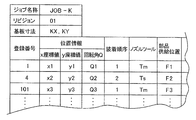
- FIG. 6 is a diagram illustrating an example of the mounting job data.
- the mounting job data creation unit first copies the job name, revision number, board dimensions, registration numbers of all electronic components, and position information of the inspection job data to the mounting job data as they are.
- the mounting job data creation unit sets items necessary for mounting for the electronic components of each registration number.
- items necessary for mounting include mounting order, nozzle tool, and component supply position.
- the mounting order represents the order in which electronic components are mounted on the original substrate.
- the nozzle tool may be replaced according to the type of electronic component.
- the electronic components with registration numbers 1 and 101 are mounted for the first time using a multi-nozzle tool Tm having a plurality of suction nozzles 41.
- the electronic component with registration number 4 is mounted a second time using a single nozzle tool Ts having one suction nozzle 41.
- the component supply position designates one of a plurality of component supply devices equipped in the electronic component mounting machine 4. It is preferable that items necessary for mounting are automatically set by an optimization program or the like. Through the above procedure, the mounting job data is completed.
- the inspection job data is transferred to the board appearance inspection machine 5 and stored. Further, the mounting job data is transferred to and stored in the electronic component mounting machine 4. As a result, preparation of job data for producing the finished product substrate K is completed. Thereafter, a setup operation for supplying members such as an original substrate and an electronic component is performed in the substrate production line 1, and production is started.
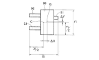
- FIG. 7 is a plan view for explaining the amount of eccentricity ( ⁇ X, ⁇ Y) of the adsorption position of the transistor component.
- ⁇ X represents the amount of eccentricity in the x-axis direction
- ⁇ Y represents the amount of eccentricity in the y-axis direction.
- the transistor component includes a main body 90, a first lead 91, a second lead 92, and a third lead 93.
- the first lead portion 91 protrudes small from one long side of the rectangular main body portion 90.
- the second lead portion 92 and the third lead portion 93 greatly extend from the other long side of the main body portion 90.
- the vertical dimension Xi of the transistor component is the horizontal dimension Yi.
- the center of gravity is decentered with respect to the center position C of the transistor component.
- the suction posture can be stabilized by decentering the suction position G near the center of gravity instead of the center position C.
- the eccentric amount ( ⁇ X, ⁇ Y) of the suction position G with respect to the center position C is registered in the component library 75.
- the electronic component mounting machine 4 makes an inquiry to the component library 75 to grasp the eccentricity ( ⁇ X, ⁇ Y), and corrects the position control of the suction nozzle 41 during suction and mounting. it can. Thereby, the electronic component mounting machine 4 can adsorb
- the mounting job data includes information on the eccentric amount ( ⁇ X, ⁇ Y) of the suction position G of the component library 75 associated with the registration number i.
- the method for creating the mounting job data uses the image image acquisition device 51 to capture a finished product substrate K on which an electronic component is already mounted on the original substrate, thereby obtaining finished product image data.
- Data is image-processed, and shape information (length dimension KX, width dimension KY, X dimension X1, Y dimension Y1) representing the shape and size of the original substrate and electronic components, and x ⁇
- shape information (length dimension KX, width dimension KY, X dimension X1, Y dimension Y1) representing the shape and size of the original substrate and electronic components, and x ⁇
- the position information x coordinate value, y coordinate value, rotation angle Q
- Mounting job data used for the electronic component mounting machine 4 is created.
- the finished product image data is acquired using the finished product substrate K as a sample, the shape information of the original substrate and the electronic component, and the position information of the electronic component are extracted, and used for the electronic component placement machine 4.
- Create job data Since all or most of the data creation procedure can be automated, the burden on the operator can be reduced as compared with the conventional procedure. In addition, the time required for data creation is also reduced compared to the conventional method. In addition, since the finished product substrate K is used as a sample instead of the original substrate, even if there is a land that is not used, an electronic component is not erroneously assigned.
- the mounting job data is a position coordinate value designated when the electronic component mounting machine 4 mounts the electronic component on the original substrate, and is an x-coordinate value and a y-coordinate value expressed using the xy coordinate system.
- And rotation angle Q, and component data including an information group including electronic component type and shape information are also clarified, so that accurate mounting is performed.
- the finished product substrate K is used as a sample, even if the actual position of the land of the original substrate has an error with respect to the CAD data, no error occurs in the designated mounting position.
- the component library 75 in which component data of a plurality of types of electronic components are registered in advance is referred to. According to this, since the parts library 75 can be used efficiently, the burden on the operator is further remarkably reduced, and the time required for data creation is further remarkably reduced.
- one electronic component is newly registered in the component library 75. According to this, when a new electronic component that has not been used is mounted on the finished product substrate K, new registration is performed each time, and the component library 75 can be enriched. For this reason, when the electronic component is used for the second time and thereafter, the burden on the operator is reduced.
- the selection operation by the operator is used together. According to this, even when the type of the electronic component cannot be specified only by referring to the X dimension and the Y size, the type of the electronic component can be correctly specified by the operator's selection operation. Furthermore, when a new electronic component with no use record is newly registered in the component library, an input operation by the operator is also used. According to this, catalog information and specifications regarding new electronic components are accurately reflected. For this reason, the precision of the component data of this electronic component improves.
- the mounting job data is the position of the suction position G with respect to the center position C.
- Information on the amount of eccentricity ( ⁇ X, ⁇ Y) is included. According to this, the electronic component mounting machine 4 can grasp the amount of eccentricity ( ⁇ X, ⁇ Y) and correct the position control at the time of suction and mounting of the suction nozzle 41, so that stable suction and mounting can be performed. .
- a board production line 1 for producing a finished product board K is configured including the electronic component mounting machine 4 and the board appearance inspection machine 5, and an image image acquisition device 51 included in the board appearance inspection machine 5 is used.
- Completed product image data is acquired, inspection job data used in the board appearance inspection machine 5 is created based on the extracted shape information and position information, and mounting job data is created based on the inspection job data. According to this, since the image acquisition device 51 of the board appearance inspection machine 5 is used, a new capital investment is unnecessary and it is economical.
- the line management device 7 has the function of the device for creating the mounting job data according to the embodiment. That is, the line management device 7 uses the image image acquisition device 51 to image a finished product substrate K on which an electronic component is already mounted on the original substrate, thereby obtaining a finished product image data, and a finished product. Image processing is performed on the image data to extract at least the shape information representing the shape and size of the original substrate and the electronic component, and the position information of the electronic component represented using the xy coordinate system set on the original substrate. An image processing unit to perform, and an inspection job data creation unit and a mounting job data creation unit that create mounting job data used in the electronic component mounting machine 4 in the process of producing a finished product substrate K based on the extracted shape information and position information And comprising.
- the line management device 7 can execute the method for creating the mounting job data according to the embodiment. Therefore, all or most of the procedure can be automated, and the burden on the operator can be reduced as compared with the conventional method.
- the processing time of the board appearance inspection apparatus tends to be longer than the processing time of the electronic component mounting machine. For this reason, if the mounting job data is created first with the above line configuration, and the inspection job data is created based on the mounting job data, the processing times of the plurality of board appearance inspection machines are not equalized, and the throughput during production decreases. There is a fear.
- the inspection job data is created in advance so as to equalize the processing time of the board visual inspection machine, and the mounting job data of the electronic component mounting machine is created based on the inspection job data. It does not decline.
Landscapes
- Engineering & Computer Science (AREA)
- Manufacturing & Machinery (AREA)
- Microelectronics & Electronic Packaging (AREA)
- Supply And Installment Of Electrical Components (AREA)
Abstract
装着ジョブデータの作成方法は、イメージ画像取得装置(51)を用いて、原基板に電子部品が実装済みの完成品基板(K)を撮像することにより、完成品画像データを取得し、完成品画像データを画像処理して、原基板および電子部品の形状および大きさを表す形状情報(X寸法X1、Y寸法Y1)、ならびに、原基板に設定された座標系を用いて表される電子部品の位置情報(x座標値、y座標値)を抽出し、抽出した形状情報および位置情報に基づき、完成品基板Kを生産する過程で電子部品装着機4に用いられる装着ジョブデータを作成する。
Description
本発明は、完成品基板を生産する過程で電子部品装着機に用いられる装着ジョブデータを作成する方法、および、装着ジョブデータを作成する装置に関する。
原基板に電子部品が実装済みの完成品基板を生産する基板生産機として、半田印刷機、電子部品装着機、リフロー機、基板検査機などがある。これらの基板生産機を連結して基板生産ラインを構築することが一般的になっている。このうち電子部品装着機は、装着ジョブデータに基づいて動作し、原基板に電子部品を装着する装着工程を担当する。装着ジョブデータは、原基板に電子部品を装着するときの位置座標値や、電子部品の種類および形状情報を含んだ部品データの情報を含んでいる。装着ジョブデータは、さらに、複数の電子部品の装着順序や、電子部品の吸着および装着を行うノズルツールの種類や、部品供給位置などの情報を含むことが一般的である。
多くの場合、装着ジョブデータは、完成品基板をCAD設計したCADデータ、および電子部品装着機の性能データに基づいて作成される。また、多くの場合、電子部品装着機の後工程に配置された外観基板検査機で用いられる検査ジョブデータも、同じCADデータ、および外観基板検査機の性能データに基づいて作成される。装着ジョブデータおよび検査ジョブデータの作成に関する技術例が特許文献1~3に開示されている。
特許文献1の実装データ作成方法は、ランドを持った原基板をイメージスキャナにて読み取り、画像データから各ランドの形状、大きさ、および中心位置などのランドデータを取得し、部品ライブラリを検索処理してランドデータに対応する電子部品を選択することにより、実装データ(装着ジョブデータ)を作成する。これによれば、部品の実装に必要な実装データを容易にかつ短時間に、しかも作業者による個人差なく高精度に作成でき、高品質な完成品基板の提供に寄与する、とされている。
また、特許文献2の実装ラインは、電子部品装着機と、基板外観検査機と、生産用データ(装着ジョブデータ)に基づいて電子部品装着機を制御する手段と、検査用データ(検査ジョブデータ)に基づいて基板外観検査機を制御する手段と、生産用データの中から検査に必要なデータを取得して検査用データを作成する手段と、を備える。これによれば、検査用データを自動的に作成でき、検査用データの作成作業を簡単に行える、とされている。
さらに、特許文献3は、電子部品装着機および基板外観検査機を備えた部品実装システムにおける処理実行方法を開示している。この処理実行方法では、実装のみに使用する実装固有データと、検査のみに使用する検査固有データと、実装および検査の双方に使用する共通データとからなる実装ライブラリを設け、実装ライブラリを参照して実装処理および検査処理を実行する。これによれば、電子部品装着機および基板外観検査機におけるデータの重複管理を回避できる、とされている。
ところで、特許文献1の技術では、ランドを持った原基板の画像データから装着ジョブデータを作成するが、装着ジョブデータを確定できないときがある。例えば、全てのランドが必ず使用されるのでなく、オプション指定の有無に依存して特定のランドに電子部品が装着されたり、装着されなかったりする場合がある。また例えば、4個のランドが四角形の頂点位置に配置されている場合がある。この場合に、2つの接続部を有する2個の電子部品が装着されるのか、4つの接続部を有する1個の部品が装着されるのか不明となることが生じ得る。してみると、装着ジョブデータを確定するためには、原基板を撮像するよりも、電子部品が実装済みの完成品基板を撮像するほうが好ましい。
また、クライアントから完成品基板の実物を供給され、CADデータの提供を受けないケースがある。このケースでは、従来、完成品基板に実装されている電子部品の配置を座標測定機などで計測しながら装着ジョブデータを作成する必要があり、作業者の負担が大きかった。さらに、CADデータよりも、完成品基板や原基板の実物に基づいて装着ジョブデータを作成した方が好ましい場合もある。例えば、原基板のランドの実際の位置がCADデータに対して誤差をもつ場合、完成品基板や原基板に基づいて装着ジョブデータを作成することにより、装着位置を指定する精度が向上する。
本発明は、上記背景技術の問題点に鑑みてなされたものであり、完成品基板を見本として装着ジョブデータを作成する場合に、作業者の負担を従来よりも軽減できる装着ジョブデータの作成方法、および作成装置を提供することを解決すべき課題とする。
本明細書で開示する装着ジョブデータの作成方法は、イメージ画像取得装置を用いて、原基板に電子部品が実装済みの完成品基板を撮像することにより、完成品画像データを取得し、前記完成品画像データを画像処理して、前記原基板および前記電子部品の形状および大きさを表す形状情報、ならびに、前記原基板に設定された座標系を用いて表される前記電子部品の位置情報を抽出し、抽出した前記形状情報および前記位置情報に基づき、前記完成品基板を生産する過程で電子部品装着機に用いられる装着ジョブデータを作成する。
また、本明細書で開示する装着ジョブデータの作成装置は、イメージ画像取得装置を用いて、原基板に電子部品が実装済みの完成品基板を撮像することにより、完成品画像データを取得する画像取得部と、前記完成品画像データを画像処理して、前記原基板および前記電子部品の少なくとも形状および大きさを表す形状情報、ならびに、前記原基板に設定された座標系を用いて表される前記電子部品の位置情報を抽出する画像処理部と、抽出した前記形状情報および前記位置情報に基づき、前記完成品基板を生産する過程で電子部品装着機に用いられる装着ジョブデータを作成するデータ作成部と、を備える。
本明細書で開示する装着ジョブデータの作成方法によれば、完成品基板を見本として完成品画像データを取得し、原基板および電子部品の形状情報、ならびに、電子部品の位置情報を抽出して、電子部品装着機に用いられる装着ジョブデータを作成する。このデータ作成の手順は、全部または大部分を自動化できるので、作業者の負担を従来よりも軽減できる。
また、本明細書で開示する装着ジョブデータの作成装置によれば、上記した装着ジョブデータの作成方法と同様の手順を実行できる。したがって、手順の全部または大部分を自動化でき、作業者の負担を従来よりも軽減できる。
(1.実施形態の装着ジョブデータの作成方法を実施する基板生産ライン1)
実施形態の装着ジョブデータの作成方法について、図1~図7を参考にして説明する。図1は、実施形態の装着ジョブデータの作成方法を実施する基板生産ライン1を模式的に示した図である。基板生産ライン1は、半田印刷機2、半田印刷検査機3、電子部品装着機4、基板外観検査機5、リフロー機6、およびライン管理装置7により構成されている。半田印刷機2からリフロー機6までは、記載した順番に列設配置されている。
実施形態の装着ジョブデータの作成方法について、図1~図7を参考にして説明する。図1は、実施形態の装着ジョブデータの作成方法を実施する基板生産ライン1を模式的に示した図である。基板生産ライン1は、半田印刷機2、半田印刷検査機3、電子部品装着機4、基板外観検査機5、リフロー機6、およびライン管理装置7により構成されている。半田印刷機2からリフロー機6までは、記載した順番に列設配置されている。
半田印刷機2は、ペースト状の半田を定められたパターン形状で原基板に印刷する。半田印刷機2と半田印刷検査機3の間は、基板搬送装置81で連結される。半田印刷検査機3は、搬送された基板の半田印刷状態を検査する。半田印刷検査機3と電子部品装着機4の間は、基板搬送装置82で連結される。電子部品装着機4は、搬送された基板の半田の上に電子部品を装着する。電子部品装着機4は、電子部品を吸着して基板の上に装着する吸着ノズル41を有する。多数の電子部品を正確にかつ効率的に装着するために、電子部品装着機4は、装着ジョブデータに基づいて動作する。電子部品装着機4と基板外観検査機5の間は、基板搬送装置83で連結される。
基板外観検査機5は、搬送された基板に装着されている電子部品の外観状態を検査する。基板外観検査機5は、基板の外観を撮像するイメージ画像取得装置51を有する。多数の電子部品を正確にかつ効率的に検査するために、基板外観検査機5は、検査ジョブデータに基づいて動作する。基板外観検査機5とリフロー機6の間は、基板搬送装置84で連結される。リフロー機6は、基板外観検査機5で正常と判定された基板の半田を再溶融させた後に固化して、接続状態を安定化する。これにより、完成品基板の生産が終了する。
ライン管理装置7は、CPUを内蔵してソフトウェアで動作するコンピュータを用いて構成される。ライン管理装置7は、表示装置71および入力装置72を有する。ライン管理装置7は、通信線73を用いて、半田印刷機2、半田印刷検査機3、電子部品装着機4、基板外観検査機5、およびリフロー機6に通信接続される。ライン管理装置7は、さらに、通信線73を用いて、外部記憶装置に記憶された部品ライブラリ75に接続される。部品ライブラリ75は、他の基板生産ラインにも共用とされる。なお、通信線73に代えて、無線通信手段を用いることもできる。図1に示される基板生産ライン1の構成は一例であって、公知の様々な形態のライン構成、例えば複数の電子部品装着機を備えるライン構成であってもよい。
(2.部品ライブラリ75)
ここで、部品ライブラリ75について説明する。図2は、部品ライブラリ75のデータ構造の例を模式的に示す図である。部品ライブラリ75には、多種類の電子部品の部品データが予め登録されている。図2に示される例で、部品ライブラリ75は、一覧表の形式にまとめられている。すなわち、部品ライブラリ75は、登録番号、電子部品の種類、形状情報、吸着位置の偏心量、および表面の輝度または色などの欄をもつ。そして、電子部品は、種類ごとに登録番号が割り当てられ、1行の各欄にそれぞれ登録情報が設定される。
ここで、部品ライブラリ75について説明する。図2は、部品ライブラリ75のデータ構造の例を模式的に示す図である。部品ライブラリ75には、多種類の電子部品の部品データが予め登録されている。図2に示される例で、部品ライブラリ75は、一覧表の形式にまとめられている。すなわち、部品ライブラリ75は、登録番号、電子部品の種類、形状情報、吸着位置の偏心量、および表面の輝度または色などの欄をもつ。そして、電子部品は、種類ごとに登録番号が割り当てられ、1行の各欄にそれぞれ登録情報が設定される。
例えば、第1行に示される登録番号1の電子部品は、チップ抵抗であって特性値は抵抗値R1である。また、登録番号1の電子部品の形状情報は、縦寸法がX1、横寸法がY1である。縦寸法および横寸法は、水平に置かれた電子部品の水平二方向の存在範囲を示し(図7のXi、Yi参照)、縦寸法≧横寸法の関係を満たす。形状情報として、電子部品の高さや重量なども登録することが可能である。さらに、登録番号1の電子部品の吸着位置の偏心量は、(0、0)である。これは、電子部品装着機4の吸着ノズル41でこの電子部品を吸着する際に、上面の中央位置を吸着することを示している。また、電子部品の表面の輝度または色の情報は、基板外観検査機5で電子部品の外形を基板の地色から見分ける際の判定値に反映される。
第1行から第3行に登録された登録番号1、登録番号2、および登録番号3の3種類の電子部品は、特性値のみが異なり、他の情報は互いに一致している。また、登録番号1、登録番号4、および登録番号5の3種類の電子部品は、特性値が同一であり、形状情報が互いに異なる。さらに、登録番号1はチップ抵抗であり、登録番号101はチップコンデンサであるが、形状情報が互いに一致している。してみると、形状情報だけに基づいて電子部品の種類を特定することはできない。
(3.実施形態の装着ジョブデータの作成方法)
実施形態の装着ジョブデータの作成方法の説明に移る。実施形態の装着ジョブデータの作成方法では、完成品基板を見本とし、基板外観検査機5のイメージ画像取得装置51を利用して、装着ジョブデータを作成する。この作成方法は、主にライン管理装置7が有する実施形態の装着ジョブデータの作成装置の機能によって実現される。ライン管理装置7は、画像取得部、画像処理部、検査ジョブデータ作成部、および装着ジョブデータ作成部の機能を有する。また、この作成方法は、基板生産ライン1の稼動の合間に実施される。これに限定されず、ライン管理装置7に接続される別のコンピュータ装置が、装着ジョブデータの作成装置の機能を有してもよい。
実施形態の装着ジョブデータの作成方法の説明に移る。実施形態の装着ジョブデータの作成方法では、完成品基板を見本とし、基板外観検査機5のイメージ画像取得装置51を利用して、装着ジョブデータを作成する。この作成方法は、主にライン管理装置7が有する実施形態の装着ジョブデータの作成装置の機能によって実現される。ライン管理装置7は、画像取得部、画像処理部、検査ジョブデータ作成部、および装着ジョブデータ作成部の機能を有する。また、この作成方法は、基板生産ライン1の稼動の合間に実施される。これに限定されず、ライン管理装置7に接続される別のコンピュータ装置が、装着ジョブデータの作成装置の機能を有してもよい。
図3は、実施形態の装着ジョブデータの作成方法の手順図である。図3の手順J1で、ライン管理装置7の画像取得部は、基板外観検査機5のイメージ画像取得装置51を用いて、完成品画像データを取得する。この前提として、作業者は、原基板に電子部品が実装済みの完成品基板Kを、基板外観検査機5に搬入する。図4は、イメージ画像取得装置51が完成品基板Kを撮像して取得した完成品画像データの一例を示すイメージ図である。
図4に示される完成品画像データによれば、長方形の完成品基板Kの一方の短辺(図4の右側)に沿ってバーコードBCDが印刷されている。バーコードBCDは、完成品基板Kの種類を特定するジョブ名称や、更新履歴回数を示すリビジョン番号の情報などを含んでいる。また、完成品基板Kの図中の左上隅および右下隅に位置マークMpが印刷されている。位置マークMpは、完成品基板Kに設定されるx-y座標系の基準となる。図4の例で、完成品基板Kの長さ方向がx軸方向となり、幅方向がy軸方向となる。当然ながら、電子部品が実装される以前の原基板でも、x-y座標系は共通となる。
完成品基板Kには、多数の電子部品が実装されている。具体的に、完成品基板Kのほぼ中央の幅方向に並んで、3個のコンデンサ部品B1が実装されている。完成品基板Kの中心から他方の短辺(図4の左側)に寄った位置に、大形で24本のリード部を有するLSI部品B2が実装されている。完成品基板Kの中心から一方の短辺に寄った位置に、8本のリード部を有する3個のIC部品B3が実装されている。また、LSI部品B2の近傍からコンデンサ部品B1に近づくx軸方向に並んで、6本のリード部を有する3個のIC部品B4が実装されている。
さらに、完成品基板KのIC部品B3の一方の長辺側(図4の上側)に、3本のリード部を有する3個のトランジスタ部品B5が実装されている。LSI部品B2の一方の短辺側には、3本のリード部を有する2個のトランジスタ部品B6が実装されている。LSI部品B2と完成品基板Kの一方の長辺との間には、5個のチップ部品B7が実装されている。完成品基板Kの右下隅の近くに、8個のチップ部品B8が実装されている。また、完成品基板Kの一方の長辺から基板外に突出するように、コネクタ部品C1が実装されている。さらに、完成品基板Kの他方の長辺(図4の下側)の左側に、コネクタ部品C2が実装されている。完成品基板Kの他方の短辺に沿って、2個のコネクタ部品C3、C4が実装されている。
図3に戻り、手順J2で、ライン管理装置7の画像処理部は、完成品画像データを画像処理して、原基板および電子部品の形状および大きさを表す形状情報、ならびに、x-y座標系を用いて表される電子部品の位置情報を抽出する。画像処理部は、まず、完成品基板Kの長さ方向の長さ寸法KX、および幅方向の幅寸法KYを抽出する。画像処理部は、次に、2個の位置マークMpを抽出し、抽出した位置に基づいてx-y座標系を較正する。
さらに、画像処理部は、個々の電子部品の形状情報、具体的には縦方向および横方向の寸法を抽出する。電子部品が実装された回転角Qの方向に関係なく、抽出された2つの寸法のうち大きい側をX寸法とし、小さい側をY寸法とする。また、これと並行して、画像処理部は、個々の電子部品の位置情報を抽出する。位置情報は、電子部品の中央位置が占めるx座標値およびy座標値で表される。さらに、位置情報は、電子部品の回転角Qの情報を含んでいる。回転角Qは、電子部品のX寸法の方向とx軸方向とが成す角度で表される。例えば、チップ部品B7の回転角Q=90°と抽出され、コネクタ部品C2の回転角Q=0°と抽出される。
次の手順J3で、ライン管理装置7の検査ジョブデータ作成部は、検査ジョブデータを作成する。図5は、検査ジョブデータの一例を示した図である。検査ジョブデータ作成部は、一番目に、抽出されたX寸法およびY寸法を部品ライブラリ75に照会して、電子部品の特定を試みる。X寸法およびY寸法に一致した縦寸法および横寸法を有する電子部品が1種類だけの場合、検査ジョブデータ作成部は、直ちに電子部品を特定して、その登録番号を確定できる。
しかしながら、寸法の照会だけでは、電子部品の種類を特定できないケースが生じる。例えば、チップ部品B7のX寸法X1、およびY寸法Y1である場合、チップ部品B7の登録番号は、1、2、3、101、および102のいずれかとなる。このとき、検査ジョブデータ作成部は、作業者に選択操作を依頼する。例えば、検査ジョブデータ作成部は、部品ライブラリ75の該当する5行を表示装置71に表示して、作業者の選択操作を待つ。作業者が入力装置72でいずれかの登録番号を選択操作すると、検査ジョブデータ作成部は、チップ部品B7の登録番号を確定できる。つまり、検査ジョブデータ作成部は、チップ部品B7の種類を正しく特定できる。
また、部品ライブラリ75に照会した結果、画像処理の誤差を考慮しても、X寸法およびY寸法に一致した縦寸法および横寸法を有する電子部品が存在しないことが生じ得る。つまり、X寸法およびY寸法を有する電子部品は、使用実績が無い新規の電子部品であるため、部品ライブラリ75に登録されていない。この場合、検査ジョブデータ作成部は、作業者に新規登録操作を依頼する。例えば、検査ジョブデータ作成部は、部品ライブラリ75の空いた行に形状情報のみを入れて表示装置71に表示し、作業者に他の欄への入力操作を依頼する。
作業者は、新規の電子部品に関するカタログ情報や仕様などを調査して、入力装置72から入力操作を行う。これにより、新規の電子部品に関する新規登録操作が完了し、部品ライブラリ75が更新される。また、検査ジョブデータ作成部は、新規の電子部品の登録番号を確定できる。
検査ジョブデータ作成部は、完成品画像データから抽出された全部の電子部品について、登録番号を確定してゆく。これにより、図5に示される検査ジョブデータに、全部の電子部品の登録番号が並ぶ。検査ジョブデータの先頭には、ジョブ名称、リビジョン番号、および完成品基板Kの基板寸法が示される。ジョブ名称の「JOB-K」およびリビジョン番号の「01」は、バーコードBCDから抽出された情報である。また、基板寸法の「KX、KY」は、画像処理部で抽出された長さ寸法KXおよび幅寸法KYである。
検査ジョブデータ作成部は、二番目に、各登録番号の電子部品に対して、抽出された位置情報を対応付ける。これにより、例えば、図5に示されるように、登録番号1の電子部品に対して、x座標値x1、y座標値y1、および回転角Q1が対応付けられる。
検査ジョブデータ作成部は、三番目に、各登録番号の電子部品に対して、検査に必要な項目を設定する。検査に必要な項目として、撮像順序、許容誤差、および外形判定条件を例示できる。撮像順序は、完成品基板Kを複数の撮像領域に分割して撮像するときに、イメージ画像取得装置51が撮像する順序を表す。図5の例で、登録番号1および登録番号101の電子部品は、初回に撮像さる。登録番号4の電子部品は、二回目に撮像される。また、許容誤差E1、許容誤差E2、および許容誤差E3は、電子部品の実際の装着位置が指定された位置情報からずれてよい限界を表す。外形判定条件Z1、外形判定条件Z2、および外形判定条件Z3は、電子部品の外形を基板の地色から見分ける際の判定値を表す。検査に必要な項目は、最適化プログラムなどによって自動設定されることが好ましい。以上の手順によって、検査ジョブデータが完成する。
次の手順J4で、ライン管理装置7の装着ジョブデータ作成部は、検査ジョブデータに基づいて装着ジョブデータを作成する。図6は、装着ジョブデータの一例を示した図である。装着ジョブデータ作成部は、一番目に、検査ジョブデータのジョブ名称、リビジョン番号、基板寸法、全部の電子部品の登録番号および位置情報をそのまま装着ジョブデータにコピーする。
装着ジョブデータ作成部は、二番目に、各登録番号の電子部品に対して、装着に必要な項目を設定する。装着に必要な項目として、装着順序、ノズルツール、および部品供給位置を例示できる。装着順序は、電子部品を原基板に装着する順序を表す。また、ノズルツールは、電子部品の種類に対応して交換されることがある。図5の例で、登録番号1および登録番号101の電子部品は、複数本の吸着ノズル41を有するマルチノズルツールTmを用いて初回に装着される。登録番号4の電子部品は、1本の吸着ノズル41を有するシングルノズルツールTsを用いて二回目に装着される。部品供給位置は、電子部品装着機4に装備される複数の部品供給装置のひとつを指定する。装着に必要な項目は、最適化プログラムなどによって自動設定されることが好ましい。以上の手順によって、装着ジョブデータが完成する。
検査ジョブデータは、基板外観検査機5に転送されて記憶される。また、装着ジョブデータは、電子部品装着機4に転送されて記憶される。これにより、完成品基板Kを生産する際のジョブデータの準備が整う。この後、基板生産ライン1で、原基板や電子部品などの部材を供給する段取り作業が行われて、生産が開始される。
ここで、図2の登録番号iに登録されたトランジスタ部品の吸着位置の偏心量(ΔX、ΔY)について追加説明する。図7は、トランジスタ部品の吸着位置の偏心量(ΔX、ΔY)を説明する平面図である。ΔXは、x軸方向の偏心量を表し、ΔYは、y軸方向の偏心量を表す。図示されるように、トランジスタ部品は、本体部90、第1リード部91、第2リード部92、および第3リード部93からなる。第1リード部91は、長方形の本体部90の一方の長辺から小さく突出している。一方、第2リード部92および第3リード部93は、本体部90の他方の長辺から大きく延び出している。トランジスタ部品の縦寸法Xiであり、横寸法Yiである。そして、トランジスタ部品の中心位置Cに対して、重心位置は偏心している。
このトランジスタ部品を吸着ノズル41で吸着する際に、吸着位置Gを中心位置Cでなく重心位置の近傍に偏心させることで、吸着姿勢を安定化できる。このため、中心位置Cに対する吸着位置Gの偏心量(ΔX、ΔY)が部品ライブラリ75に登録される。装着ジョブデータに登録番号iが有るとき、電子部品装着機4は、部品ライブラリ75に照会して偏心量(ΔX、ΔY)を把握し、吸着ノズル41の吸着時および装着時の位置制御を補正できる。これにより、電子部品装着機4は、このトランジスタ部品を安定して吸着および装着できる。上述のように、装着ジョブデータは、登録番号iによって対応付けられた部品ライブラリ75の吸着位置Gの偏心量(ΔX、ΔY)の情報を含んでいる。
(4.実施形態の装着ジョブデータの作成方法の態様および効果)
実施形態の装着ジョブデータの作成方法は、イメージ画像取得装置51を用いて、原基板に電子部品が実装済みの完成品基板Kを撮像することにより、完成品画像データを取得し、完成品画像データを画像処理して、原基板および電子部品の形状および大きさを表す形状情報(長さ寸法KX、幅寸法KY、X寸法X1、Y寸法Y1)、ならびに、原基板に設定されたx-y座標系を用いて表される電子部品の位置情報(x座標値、y座標値、回転角Q)を抽出し、抽出した形状情報および位置情報に基づき、完成品基板Kを生産する過程で電子部品装着機4に用いられる装着ジョブデータを作成する。
実施形態の装着ジョブデータの作成方法は、イメージ画像取得装置51を用いて、原基板に電子部品が実装済みの完成品基板Kを撮像することにより、完成品画像データを取得し、完成品画像データを画像処理して、原基板および電子部品の形状および大きさを表す形状情報(長さ寸法KX、幅寸法KY、X寸法X1、Y寸法Y1)、ならびに、原基板に設定されたx-y座標系を用いて表される電子部品の位置情報(x座標値、y座標値、回転角Q)を抽出し、抽出した形状情報および位置情報に基づき、完成品基板Kを生産する過程で電子部品装着機4に用いられる装着ジョブデータを作成する。
これによれば、完成品基板Kを見本として完成品画像データを取得し、原基板および電子部品の形状情報、ならびに、電子部品の位置情報を抽出して、電子部品装着機4に用いられる装着ジョブデータを作成する。このデータ作成の手順は、全部または大部分を自動化できるので、作業者の負担を従来よりも軽減できる。また、データ作成の所要時間も、従来と比較して削減される。また、原基板でなく完成品基板Kを見本とするので、使用されないランドがある場合でも、誤って電子部品を割り付けることがない。
さらに、装着ジョブデータは、電子部品装着機4が電子部品を原基板に装着するときに指定する位置座標値であって、x-y座標系を用いて表されるx座標値、y座標値、および回転角Q、ならびに、電子部品の種類および形状情報を含んだ情報群からなる部品データを含む。これによれば、装着ジョブデータによって電子部品の装着位置が指定されるとともに、電子部品の種類および形状情報も明らかになるので、正確な装着が行われる。また、完成品基板Kを見本とするので、原基板のランドの実際の位置がCADデータに対して誤差をもつ場合でも、指定される装着位置に誤差は発生しない。
さらに、装着ジョブデータを作成するときに、複数種類の電子部品の部品データが予め登録された部品ライブラリ75を参照する。これによれば、部品ライブラリ75を効率的に利用できるので、作業者の負担は、さらに顕著に軽減され、データ作成の所要時間も、さらに顕著に削減される。
また、完成品画像データから抽出した一つの電子部品の形状情報が部品ライブラリ75に登録されていない場合に、一つの電子部品を部品ライブラリ75に新規登録する。これによれば、使用実績の無い新規の電子部品が完成品基板Kに実装されていた場合に、その都度新規登録を行って、部品ライブラリ75を充実させることができる。このため、この電子部品の2回目以降の使用では、作業者の負担が軽減される。
また、部品ライブラリ75を参照する際に、作業者による選択操作を併用する。これによれば、X寸法およびY寸法の照会だけで電子部品の種類を特定できない場合でも、作業者の選択操作によって、電子部品の種類を正しく特定できる。さらに、使用実績の無い新規の電子部品を部品ライブラリに新規登録する際に、作業者による入力操作を併用する。これによれば、新規の電子部品に関するカタログ情報や仕様などが正確に反映される。このため、この電子部品の部品データの精度が向上する。
さらに、電子部品(トランジスタ部品)の中心位置Cに対して、電子部品装着機4の吸着ノズル41で吸着する吸着位置Gを偏心させる場合に、装着ジョブデータは、中心位置Cに対する吸着位置Gの偏心量(ΔX、ΔY)の情報を含む。これによれば、電子部品装着機4は、偏心量(ΔX、ΔY)を把握して、吸着ノズル41の吸着時および装着時の位置制御を補正できるので、安定した吸着および装着が可能になる。
さらに、電子部品装着機4および基板外観検査機5を含んで、完成品基板Kを生産する基板生産ライン1が構成されており、基板外観検査機5が有するイメージ画像取得装置51を用いて、完成品画像データを取得し、抽出した形状情報および位置情報に基づき、基板外観検査機5に用いられる検査ジョブデータを作成し、検査ジョブデータに基づいて装着ジョブデータを作成する。これによれば、基板外観検査機5のイメージ画像取得装置51を利用するため、新たな設備投資が不要であって経済的である。
また、ライン管理装置7は、実施形態の装着ジョブデータの作成装置の機能を有する。すなわち、ライン管理装置7は、イメージ画像取得装置51を用いて、原基板に電子部品が実装済みの完成品基板Kを撮像することにより、完成品画像データを取得する画像取得部と、完成品画像データを画像処理して、原基板および電子部品の少なくとも形状および大きさを表す形状情報、ならびに、原基板に設定されたx-y座標系を用いて表される電子部品の位置情報を抽出する画像処理部と、抽出した形状情報および位置情報に基づき、完成品基板Kを生産する過程で電子部品装着機4に用いられる装着ジョブデータを作成する検査ジョブデータ作成部および装着ジョブデータ作成部と、を備える。
これによれば、ライン管理装置7は、実施形態の装着ジョブデータの作成方法を実行できる。したがって、手順の全部または大部分を自動化でき、作業者の負担を従来よりも軽減できる。
(5.実施形態の応用および変形)
なお、基板生産ラインに基板外観検査機が複数台配置され、それぞれの基板外観検査機の前工程に電子部品装着機が配置されたライン構成に対して、適切な応用例がある。詳述すると、完成品画像データから抽出された全部の電子部品を複数の基板外観検査機に分配して、それぞれの検査ジョブデータを作成する。分配処理は、最適化プログラムを用いて行なわれ、複数台の基板外観検査機の間で、検査に必要な処理時間が均等化される。このように作成された検査ジョブデータに基づいて、各基板外観検査機の前工程に配置された電子部品装着機の装着ジョブデータをそれぞれ作成する。
なお、基板生産ラインに基板外観検査機が複数台配置され、それぞれの基板外観検査機の前工程に電子部品装着機が配置されたライン構成に対して、適切な応用例がある。詳述すると、完成品画像データから抽出された全部の電子部品を複数の基板外観検査機に分配して、それぞれの検査ジョブデータを作成する。分配処理は、最適化プログラムを用いて行なわれ、複数台の基板外観検査機の間で、検査に必要な処理時間が均等化される。このように作成された検査ジョブデータに基づいて、各基板外観検査機の前工程に配置された電子部品装着機の装着ジョブデータをそれぞれ作成する。
通常、基板外観検査装置の処理時間は、電子部品装着機の処理時間よりも大きくなる傾向にある。そのため、上記のライン構成で、先に装着ジョブデータを作成し、それに基づいて検査ジョブデータを作成すると、複数台の基板外観検査機の処理時間が均等化されず、生産時のスループットが低下するおそれがある。本応用例によれば、基板外観検査機の処理時間を均等化するように先に検査ジョブデータを作成し、それに基づいて電子部品装着機の装着ジョブデータを作成するので、生産時のスループットが低下しない。
また、検査ジョブデータおよび装着ジョブデータの一方のみを作成する用途とすることもできる。さらに、基板外観検査機5のイメージ画像取得装置51およびライン管理装置7に代えて、基板生産ライン1に関係ない別のイメージ画像取得装置およびコンピュータ装置を用いることも可能である。この場合、装着ジョブデータの作成方法を実施しても、基板生産ライン1の稼動に影響を及ぼさない。本発明は、その他にも様々な応用や変形が可能である。
1:基板生産ライン 4:電子部品装着機 41:吸着ノズル 5:基板外観検査機 51:イメージ画像取得装置 7:ライン管理装置 75:部品ライブラリ K:完成品基板 Mp:位置マーク KX:長さ寸法 KY:幅寸法 B7:チップ部品 X1:X寸法 Y1:Y寸法 (ΔX、ΔY):偏心量 C:中心位置 G:吸着位置
Claims (8)
- イメージ画像取得装置を用いて、原基板に電子部品が実装済みの完成品基板を撮像することにより、完成品画像データを取得し、
前記完成品画像データを画像処理して、前記原基板および前記電子部品の形状および大きさを表す形状情報、ならびに、前記原基板に設定された座標系を用いて表される前記電子部品の位置情報を抽出し、
抽出した前記形状情報および前記位置情報に基づき、前記完成品基板を生産する過程で電子部品装着機に用いられる装着ジョブデータを作成する、
装着ジョブデータの作成方法。 - 前記装着ジョブデータは、
前記電子部品装着機が前記電子部品を前記原基板に装着するときに指定する位置座標値であって、前記座標系を用いて表される位置座標値、ならびに、
前記電子部品の種類および前記形状情報を含んだ情報群からなる部品データを含む、
請求項1に記載の装着ジョブデータの作成方法。 - 前記装着ジョブデータを作成するときに、複数種類の前記電子部品の前記部品データが予め登録された部品ライブラリを参照する請求項2に記載の装着ジョブデータの作成方法。
- 前記完成品画像データから抽出した一つの前記電子部品の前記形状情報が前記部品ライブラリに登録されていない場合に、一つの前記電子部品を前記部品ライブラリに新規登録する請求項3に記載の装着ジョブデータの作成方法。
- 請求項3に記載の装着ジョブデータの作成方法で前記部品ライブラリを参照する際に、または、請求項4に記載の装着ジョブデータの作成方法で一つの前記電子部品を新規登録する際に、作業者による操作を併用する装着ジョブデータの作成方法。
- 前記電子部品の中心位置に対して、前記電子部品装着機の吸着ノズルで吸着する吸着位置を偏心させる場合に、
前記装着ジョブデータは、前記中心位置に対する前記吸着位置の偏心量の情報を含む請求項1~5のいずれか一項に記載の装着ジョブデータの作成方法。 - 前記電子部品装着機および基板外観検査機を含んで、前記完成品基板を生産する基板生産ラインが構成されており、
前記基板外観検査機が有する前記イメージ画像取得装置を用いて、前記完成品画像データを取得し、
抽出した前記形状情報および前記位置情報に基づき、前記基板外観検査機に用いられる検査ジョブデータを作成し、
前記検査ジョブデータに基づいて前記装着ジョブデータを作成する請求項1~6のいずれか一項に記載の装着ジョブデータの作成方法。 - イメージ画像取得装置を用いて、原基板に電子部品が実装済みの完成品基板を撮像することにより、完成品画像データを取得する画像取得部と、
前記完成品画像データを画像処理して、前記原基板および前記電子部品の少なくとも形状および大きさを表す形状情報、ならびに、前記原基板に設定された座標系を用いて表される前記電子部品の位置情報を抽出する画像処理部と、
抽出した前記形状情報および前記位置情報に基づき、前記完成品基板を生産する過程で電子部品装着機に用いられる装着ジョブデータを作成するデータ作成部と、
を備える装着ジョブデータの作成装置。
Priority Applications (2)
| Application Number | Priority Date | Filing Date | Title |
|---|---|---|---|
| PCT/JP2016/086714 WO2018105100A1 (ja) | 2016-12-09 | 2016-12-09 | 装着ジョブデータの作成方法および作成装置 |
| JP2018555413A JP6792638B2 (ja) | 2016-12-09 | 2016-12-09 | 装着ジョブデータの作成方法および作成装置 |
Applications Claiming Priority (1)
| Application Number | Priority Date | Filing Date | Title |
|---|---|---|---|
| PCT/JP2016/086714 WO2018105100A1 (ja) | 2016-12-09 | 2016-12-09 | 装着ジョブデータの作成方法および作成装置 |
Publications (1)
| Publication Number | Publication Date |
|---|---|
| WO2018105100A1 true WO2018105100A1 (ja) | 2018-06-14 |
Family
ID=62491535
Family Applications (1)
| Application Number | Title | Priority Date | Filing Date |
|---|---|---|---|
| PCT/JP2016/086714 Ceased WO2018105100A1 (ja) | 2016-12-09 | 2016-12-09 | 装着ジョブデータの作成方法および作成装置 |
Country Status (2)
| Country | Link |
|---|---|
| JP (1) | JP6792638B2 (ja) |
| WO (1) | WO2018105100A1 (ja) |
Cited By (2)
| Publication number | Priority date | Publication date | Assignee | Title |
|---|---|---|---|---|
| WO2020183516A1 (ja) * | 2019-03-08 | 2020-09-17 | ヤマハ発動機株式会社 | 実装データ作成支援装置、実装データ作成支援方法、外観検査機、部品実装システム |
| WO2022003919A1 (ja) * | 2020-07-02 | 2022-01-06 | ヤマハ発動機株式会社 | 検査データ作成方法、検査データ作成装置および検査装置 |
Citations (6)
| Publication number | Priority date | Publication date | Assignee | Title |
|---|---|---|---|---|
| JPH09190531A (ja) * | 1996-01-09 | 1997-07-22 | Matsushita Electric Ind Co Ltd | 実装データ作成方法と装置、および基板と実装の検査方法 |
| JP2000031693A (ja) * | 1998-07-10 | 2000-01-28 | Sanyo Electric Co Ltd | 電子部品の吸着部位教示装置 |
| JP2002134995A (ja) * | 2001-07-26 | 2002-05-10 | Matsushita Electric Ind Co Ltd | 実装データ作成装置及び実装機 |
| JP2004356574A (ja) * | 2003-05-30 | 2004-12-16 | Xanavi Informatics Corp | 基板情報作成方法および基板情報作成装置 |
| JP2005216889A (ja) * | 2004-01-27 | 2005-08-11 | Yamaha Motor Co Ltd | 電子部品実装データの作成方法および同装置 |
| WO2009150721A1 (ja) * | 2008-06-10 | 2009-12-17 | パイオニア株式会社 | 電子部品実装データの作成方法及び作成装置 |
Family Cites Families (3)
| Publication number | Priority date | Publication date | Assignee | Title |
|---|---|---|---|---|
| JPH06164189A (ja) * | 1992-11-25 | 1994-06-10 | Matsushita Electric Ind Co Ltd | 実装ラインの実装部品振り分け方法 |
| JPH0862275A (ja) * | 1994-08-24 | 1996-03-08 | Matsushita Electric Ind Co Ltd | 実装検査データ作成方法 |
| CN104620690A (zh) * | 2012-09-12 | 2015-05-13 | 富士机械制造株式会社 | 对基板作业系统、作业顺序最佳化程序、作业台数决定程序 |
-
2016
- 2016-12-09 WO PCT/JP2016/086714 patent/WO2018105100A1/ja not_active Ceased
- 2016-12-09 JP JP2018555413A patent/JP6792638B2/ja active Active
Patent Citations (6)
| Publication number | Priority date | Publication date | Assignee | Title |
|---|---|---|---|---|
| JPH09190531A (ja) * | 1996-01-09 | 1997-07-22 | Matsushita Electric Ind Co Ltd | 実装データ作成方法と装置、および基板と実装の検査方法 |
| JP2000031693A (ja) * | 1998-07-10 | 2000-01-28 | Sanyo Electric Co Ltd | 電子部品の吸着部位教示装置 |
| JP2002134995A (ja) * | 2001-07-26 | 2002-05-10 | Matsushita Electric Ind Co Ltd | 実装データ作成装置及び実装機 |
| JP2004356574A (ja) * | 2003-05-30 | 2004-12-16 | Xanavi Informatics Corp | 基板情報作成方法および基板情報作成装置 |
| JP2005216889A (ja) * | 2004-01-27 | 2005-08-11 | Yamaha Motor Co Ltd | 電子部品実装データの作成方法および同装置 |
| WO2009150721A1 (ja) * | 2008-06-10 | 2009-12-17 | パイオニア株式会社 | 電子部品実装データの作成方法及び作成装置 |
Cited By (4)
| Publication number | Priority date | Publication date | Assignee | Title |
|---|---|---|---|---|
| WO2020183516A1 (ja) * | 2019-03-08 | 2020-09-17 | ヤマハ発動機株式会社 | 実装データ作成支援装置、実装データ作成支援方法、外観検査機、部品実装システム |
| JPWO2020183516A1 (ja) * | 2019-03-08 | 2021-10-14 | ヤマハ発動機株式会社 | 実装データ作成支援装置、実装データ作成支援方法、外観検査機、部品実装システム |
| JP7427652B2 (ja) | 2019-03-08 | 2024-02-05 | ヤマハ発動機株式会社 | 実装データ作成支援装置、実装データ作成支援方法、外観検査機および制御装置からなるシステムおよび部品実装システム |
| WO2022003919A1 (ja) * | 2020-07-02 | 2022-01-06 | ヤマハ発動機株式会社 | 検査データ作成方法、検査データ作成装置および検査装置 |
Also Published As
| Publication number | Publication date |
|---|---|
| JP6792638B2 (ja) | 2020-11-25 |
| JPWO2018105100A1 (ja) | 2019-08-08 |
Similar Documents
| Publication | Publication Date | Title |
|---|---|---|
| JP5918622B2 (ja) | 部品または基板の作業装置および部品実装装置 | |
| JP5751584B2 (ja) | 電子部品実装装置 | |
| JP2015135886A (ja) | 管理装置 | |
| EP2931014B1 (en) | Apparatus and method for generating mounting data, and substrate manufacturing system | |
| KR101314142B1 (ko) | 기판 처리 장치 및 기판 처리 시스템 | |
| JP6792638B2 (ja) | 装着ジョブデータの作成方法および作成装置 | |
| JP4629584B2 (ja) | 実装システムおよび電子部品の実装方法 | |
| WO2018216101A1 (ja) | 装着順序決定装置、装着順序検査装置、装着順序決定方法、および装着順序検査方法 | |
| JP6734868B2 (ja) | 基板用の画像処理装置および画像処理方法 | |
| JP5845448B2 (ja) | 生産データ作成装置および生産データ作成方法 | |
| JP6473172B2 (ja) | 対基板作業機 | |
| JP4896855B2 (ja) | 部品実装システム | |
| WO2017081773A1 (ja) | 基板用の画像処理装置および画像処理方法 | |
| CN109196971B (zh) | 元件安装系统 | |
| JP6948406B2 (ja) | 電子部品装着向き確認システム及び電子部品装着向き確認方法 | |
| JPWO2017072908A1 (ja) | 基板位置検索装置、および部品実装機 | |
| CN102238864A (zh) | 电子元件安装方法、电子元件安装装置及嘴数据生成方法 | |
| JP6862221B2 (ja) | 装着使用データ管理装置 | |
| EP3606313A1 (en) | Substrate-related work machine | |
| JP6735208B2 (ja) | キャリブレーション治具、板金搬入システム、及びキャリブレーション方法 | |
| JP7232894B2 (ja) | 実装システム | |
| JP7427652B2 (ja) | 実装データ作成支援装置、実装データ作成支援方法、外観検査機および制御装置からなるシステムおよび部品実装システム | |
| JP6928461B2 (ja) | 装着使用データ管理装置 | |
| JP3916860B2 (ja) | プリント基板組立装置 | |
| US20210173546A1 (en) | Information processing device and information processing method |
Legal Events
| Date | Code | Title | Description |
|---|---|---|---|
| 121 | Ep: the epo has been informed by wipo that ep was designated in this application |
Ref document number: 16923362 Country of ref document: EP Kind code of ref document: A1 |
|
| ENP | Entry into the national phase |
Ref document number: 2018555413 Country of ref document: JP Kind code of ref document: A |
|
| NENP | Non-entry into the national phase |
Ref country code: DE |
|
| 122 | Ep: pct application non-entry in european phase |
Ref document number: 16923362 Country of ref document: EP Kind code of ref document: A1 |