WO2018092454A1 - インプリント装置、インプリント方法及び物品の製造方法 - Google Patents
インプリント装置、インプリント方法及び物品の製造方法 Download PDFInfo
- Publication number
- WO2018092454A1 WO2018092454A1 PCT/JP2017/036246 JP2017036246W WO2018092454A1 WO 2018092454 A1 WO2018092454 A1 WO 2018092454A1 JP 2017036246 W JP2017036246 W JP 2017036246W WO 2018092454 A1 WO2018092454 A1 WO 2018092454A1
- Authority
- WO
- WIPO (PCT)
- Prior art keywords
- mold
- substrate
- imprint
- gas
- stage
- Prior art date
- Legal status (The legal status is an assumption and is not a legal conclusion. Google has not performed a legal analysis and makes no representation as to the accuracy of the status listed.)
- Ceased
Links
Images


Classifications
-
- G—PHYSICS
- G03—PHOTOGRAPHY; CINEMATOGRAPHY; ANALOGOUS TECHNIQUES USING WAVES OTHER THAN OPTICAL WAVES; ELECTROGRAPHY; HOLOGRAPHY
- G03F—PHOTOMECHANICAL PRODUCTION OF TEXTURED OR PATTERNED SURFACES, e.g. FOR PRINTING, FOR PROCESSING OF SEMICONDUCTOR DEVICES; MATERIALS THEREFOR; ORIGINALS THEREFOR; APPARATUS SPECIALLY ADAPTED THEREFOR
- G03F7/00—Photomechanical, e.g. photolithographic, production of textured or patterned surfaces, e.g. printing surfaces; Materials therefor, e.g. comprising photoresists; Apparatus specially adapted therefor
- G03F7/0002—Lithographic processes using patterning methods other than those involving the exposure to radiation, e.g. by stamping
-
- B—PERFORMING OPERATIONS; TRANSPORTING
- B05—SPRAYING OR ATOMISING IN GENERAL; APPLYING FLUENT MATERIALS TO SURFACES, IN GENERAL
- B05C—APPARATUS FOR APPLYING FLUENT MATERIALS TO SURFACES, IN GENERAL
- B05C9/00—Apparatus or plant for applying liquid or other fluent material to surfaces by means not covered by any preceding group, or in which the means of applying the liquid or other fluent material is not important
- B05C9/08—Apparatus or plant for applying liquid or other fluent material to surfaces by means not covered by any preceding group, or in which the means of applying the liquid or other fluent material is not important for applying liquid or other fluent material and performing an auxiliary operation
-
- B—PERFORMING OPERATIONS; TRANSPORTING
- B29—WORKING OF PLASTICS; WORKING OF SUBSTANCES IN A PLASTIC STATE IN GENERAL
- B29C—SHAPING OR JOINING OF PLASTICS; SHAPING OF MATERIAL IN A PLASTIC STATE, NOT OTHERWISE PROVIDED FOR; AFTER-TREATMENT OF THE SHAPED PRODUCTS, e.g. REPAIRING
- B29C59/00—Surface shaping of articles, e.g. embossing; Apparatus therefor
- B29C59/02—Surface shaping of articles, e.g. embossing; Apparatus therefor by mechanical means, e.g. pressing
-
- G—PHYSICS
- G03—PHOTOGRAPHY; CINEMATOGRAPHY; ANALOGOUS TECHNIQUES USING WAVES OTHER THAN OPTICAL WAVES; ELECTROGRAPHY; HOLOGRAPHY
- G03F—PHOTOMECHANICAL PRODUCTION OF TEXTURED OR PATTERNED SURFACES, e.g. FOR PRINTING, FOR PROCESSING OF SEMICONDUCTOR DEVICES; MATERIALS THEREFOR; ORIGINALS THEREFOR; APPARATUS SPECIALLY ADAPTED THEREFOR
- G03F7/00—Photomechanical, e.g. photolithographic, production of textured or patterned surfaces, e.g. printing surfaces; Materials therefor, e.g. comprising photoresists; Apparatus specially adapted therefor
- G03F7/16—Coating processes; Apparatus therefor
- G03F7/168—Finishing the coated layer, e.g. drying, baking, soaking
-
- G—PHYSICS
- G03—PHOTOGRAPHY; CINEMATOGRAPHY; ANALOGOUS TECHNIQUES USING WAVES OTHER THAN OPTICAL WAVES; ELECTROGRAPHY; HOLOGRAPHY
- G03F—PHOTOMECHANICAL PRODUCTION OF TEXTURED OR PATTERNED SURFACES, e.g. FOR PRINTING, FOR PROCESSING OF SEMICONDUCTOR DEVICES; MATERIALS THEREFOR; ORIGINALS THEREFOR; APPARATUS SPECIALLY ADAPTED THEREFOR
- G03F7/00—Photomechanical, e.g. photolithographic, production of textured or patterned surfaces, e.g. printing surfaces; Materials therefor, e.g. comprising photoresists; Apparatus specially adapted therefor
- G03F7/70—Microphotolithographic exposure; Apparatus therefor
- G03F7/70691—Handling of masks or workpieces
- G03F7/70716—Stages
-
- G—PHYSICS
- G03—PHOTOGRAPHY; CINEMATOGRAPHY; ANALOGOUS TECHNIQUES USING WAVES OTHER THAN OPTICAL WAVES; ELECTROGRAPHY; HOLOGRAPHY
- G03F—PHOTOMECHANICAL PRODUCTION OF TEXTURED OR PATTERNED SURFACES, e.g. FOR PRINTING, FOR PROCESSING OF SEMICONDUCTOR DEVICES; MATERIALS THEREFOR; ORIGINALS THEREFOR; APPARATUS SPECIALLY ADAPTED THEREFOR
- G03F7/00—Photomechanical, e.g. photolithographic, production of textured or patterned surfaces, e.g. printing surfaces; Materials therefor, e.g. comprising photoresists; Apparatus specially adapted therefor
- G03F7/70—Microphotolithographic exposure; Apparatus therefor
- G03F7/708—Construction of apparatus, e.g. environment aspects, hygiene aspects or materials
- G03F7/70808—Construction details, e.g. housing, load-lock, seals or windows for passing light in or out of apparatus
- G03F7/70825—Mounting of individual elements, e.g. mounts, holders or supports
-
- H—ELECTRICITY
- H01—ELECTRIC ELEMENTS
- H01L—SEMICONDUCTOR DEVICES NOT COVERED BY CLASS H10
- H01L21/00—Processes or apparatus adapted for the manufacture or treatment of semiconductor or solid state devices or of parts thereof
- H01L21/02—Manufacture or treatment of semiconductor devices or of parts thereof
- H01L21/027—Making masks on semiconductor bodies for further photolithographic processing not provided for in group H01L21/18 or H01L21/34
- H01L21/0271—Making masks on semiconductor bodies for further photolithographic processing not provided for in group H01L21/18 or H01L21/34 comprising organic layers
-
- H—ELECTRICITY
- H01—ELECTRIC ELEMENTS
- H01L—SEMICONDUCTOR DEVICES NOT COVERED BY CLASS H10
- H01L21/00—Processes or apparatus adapted for the manufacture or treatment of semiconductor or solid state devices or of parts thereof
- H01L21/67—Apparatus specially adapted for handling semiconductor or electric solid state devices during manufacture or treatment thereof; Apparatus specially adapted for handling wafers during manufacture or treatment of semiconductor or electric solid state devices or components ; Apparatus not specifically provided for elsewhere
- H01L21/67005—Apparatus not specifically provided for elsewhere
- H01L21/67011—Apparatus for manufacture or treatment
- H01L21/67017—Apparatus for fluid treatment
- H01L21/67063—Apparatus for fluid treatment for etching
Definitions
- the present invention relates to an imprint apparatus, an imprint method, and an article manufacturing method.
- the demand for miniaturization of semiconductor devices, MEMS, and the like has advanced, and in addition to the conventional photolithography technology, an imprint technology capable of forming a fine pattern (structure) on the order of several nanometers on a substrate has attracted attention. Yes.
- the imprint technology supplies (applies) an uncured imprint material onto a substrate, contacts the imprint material with a mold (mold), and corresponds to a fine uneven pattern formed on the mold. This is a fine processing technique for forming a material pattern on a substrate.
- the imprint material supplied to the shot area on the substrate is in contact with the mold to irradiate light to cure the imprint material, and the mold is removed from the cured imprint material.
- JP 2007-98779 A Japanese Patent No. 5235506
- the ion concentration of the gas is lowered in the process of supplying the ionized gas between the mold and the substrate.
- the decrease in ion concentration becomes significant. If a sufficient ion concentration cannot be maintained before the ionized gas reaches the mold that is the object of charge removal, it is difficult to remove the mold efficiently.
- the present invention provides an imprint apparatus that is advantageous for discharging a mold.
- An imprint apparatus is an imprint apparatus that forms a pattern on the substrate by curing the imprint material in a state where the mold and the imprint material on the substrate are in contact with each other.
- a stage that holds and moves the substrate, a peripheral member that is disposed around a portion of the stage on which the substrate is held and has a conductive surface on the mold side, and between the mold and the substrate
- a gas supply unit that supplies a gas to the space
- a dispenser that supplies an imprint material to the substrate
- a control unit that controls the movement of the stage and the supply of gas by the gas supply unit.
- the supply unit and the dispenser are arranged with a holding unit holding the mold interposed therebetween, and the control unit separates the cured imprint material and the mold from each other. Then, before the stage starts to move below the dispenser, the gas supply unit starts supplying the gas, and the peripheral member is moved to the mold through the gas during the stage movement. The neutralization of the mold is performed by making it face each other.
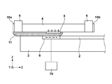
- FIG. 1 is a schematic diagram showing a configuration of an imprint apparatus 1 as one aspect of the present invention.
- the imprint apparatus 1 is a lithographic apparatus that is used for manufacturing a semiconductor device as an article and forms a pattern of an imprint material on a substrate using a mold.
- the imprint apparatus 1 makes the imprint material supplied on the substrate come into contact with the mold, and gives a curing energy to the imprint material, whereby a cured product to which the uneven pattern of the mold is transferred. The pattern is formed.
- a curable composition (also referred to as an uncured resin) that cures when given energy for curing is used.
- energy for curing electromagnetic waves, heat, or the like is used.
- the electromagnetic wave for example, light such as infrared rays, visible rays, and ultraviolet rays, whose wavelength is selected from a range of 10 nm to 1 mm is used.
- the curable composition is a composition that is cured by light irradiation or by heating.
- the photocurable composition that is cured by light irradiation contains at least a polymerizable compound and a photopolymerization initiator, and may contain a non-polymerizable compound or a solvent as necessary.
- the non-polymerizable compound is at least one selected from the group consisting of a sensitizer, a hydrogen donor, an internal release agent, a surfactant, an antioxidant, and a polymer component.
- the imprint material may be applied in the form of a film on the substrate by a spin coater or a slit coater. Further, the imprint material may be applied onto the substrate in the form of droplets by the liquid ejecting head, or in the form of islands or films formed by connecting a plurality of droplets.
- the imprint material has a viscosity (viscosity at 25 ° C.) of, for example, 1 mPa ⁇ s or more and 100 mPa ⁇ s or less.
- the imprint apparatus 1 employs a photocuring method as a method for curing the imprint material.
- the imprint apparatus 1 includes an irradiation unit 20, a mold holding unit 6, a substrate stage 3, a dispenser 7, and a control unit 50.
- the direction parallel to the optical axis of the irradiation unit 20 that irradiates the ultraviolet ray 21 to the imprint material 8 on the substrate is defined as the Z axis, and the directions orthogonal to each other in a plane perpendicular to the Z axis are defined as the X axis and the Y axis. To do.
- the irradiation unit 20 irradiates the imprint material 8 on the substrate with ultraviolet rays 21 through the mold 4 when the imprint material 8 on the substrate is cured.
- the irradiation unit 20 includes, for example, a light source (not shown) and an optical system that adjusts the ultraviolet rays 21 emitted from the light source to light suitable for curing the imprint material 8.
- the mold 4 has a rectangular outer peripheral shape, and has a pattern portion 5 in which a concavo-convex pattern (for example, a circuit pattern) to be transferred to the substrate 2 is three-dimensionally formed on a surface facing the substrate 2.
- the mold 4 is made of a material that can transmit the ultraviolet light 21, for example, quartz.
- the mold holding unit 6 holds and moves the mold 4.
- the mold holding unit 6 holds the mold 4 by attracting the outer peripheral area of the irradiation surface of the ultraviolet ray 21 in the mold 4 with a vacuum adsorption force or an electrostatic force.
- the mold holding unit 6 is configured to move the mold 4 to each axis so that the mold 4 and the imprint material 8 on the substrate can be selectively contacted (imprinted) and the mold 4 can be separated from the imprint material 8 (release). Move in the direction.
- the mold holding unit 6 may include a plurality of drive systems such as a coarse drive system and a fine drive system in order to realize highly accurate positioning of the mold 4.
- the mold holding unit 6 may have a function of moving the mold 4 not only in the Z-axis direction but also in the X-axis direction, the Y-axis direction, and the ⁇ direction of each axis, and a function of correcting the tilt of the mold 4. Good.
- the imprint apparatus 1 may perform the stamping and releasing by moving the mold 4 in the Z-axis direction as in this embodiment, but moving the substrate 2 (substrate stage 3) in the Z-axis direction. It may be realized. Moreover, you may implement
- the substrate 2 is made of glass, ceramics, metal, semiconductor, resin, or the like, and if necessary, a member made of a material different from the substrate may be formed on the surface thereof.
- the substrate 2 is a silicon wafer, a compound semiconductor wafer, quartz glass, or the like.
- An imprint material 8 formed by the pattern portion 5 of the mold 4 is supplied to the substrate 2.
- the substrate stage 3 moves while holding the substrate 2.
- the substrate stage 3 is used for positioning the mold 4 and the substrate 2 when the mold 4 and the imprint material 8 on the substrate are brought into contact with each other.
- the substrate stage 3 moves the substrate 2 in each axial direction.
- the substrate stage 3 may include a plurality of drive systems such as a coarse drive system and a fine drive system in each direction of the X axis and the Y axis.
- the substrate stage 3 may have a function of moving the substrate 2 in the Z-axis direction and the ⁇ direction of each axis and a function of correcting the tilt of the substrate 2.
- the dispenser 7 is disposed in the vicinity of the mold holding unit 6 and supplies (discharges) the imprint material 8 to the substrate 2.
- the imprint material 8 has a property of being cured by the irradiation of the ultraviolet rays 21, but the type thereof is appropriately selected according to various conditions such as a semiconductor device manufacturing process.
- the amount of the imprint material 8 discharged from the dispenser 7 is appropriately determined according to the thickness of the imprint material 8 to be formed on the substrate (residual film thickness), the density of the pattern to be formed on the substrate, and the like. Is done.
- the control unit 50 includes a CPU, a memory, and the like, and controls each unit of the imprint apparatus 1 to operate the imprint apparatus 1. Specifically, first, the imprint material 8 is supplied to the substrate 2, and the mold 4 and the substrate 2 are positioned in a predetermined positional relationship. Then, the mold 4 is moved in the ⁇ Z direction to bring the mold 4 (pattern part 5) into contact with the imprint material 8 on the substrate. By curing the imprint material 8 in a state where the mold 4 and the imprint material 8 on the substrate are in contact with each other, moving the mold 4 in the + Z direction and pulling the mold 4 away from the cured imprint material 8 on the substrate. Then, a pattern of the imprint material 8 is formed on the substrate.
- the mold 4 and the imprint material 8 on the substrate are brought into contact with each other with foreign matters such as particles attached to the mold 4 (pattern part 5), a defect is generated in the pattern formed on the substrate, The mold 4 may be damaged.
- the imprint apparatus 1 is disposed in a clean environment for manufacturing semiconductor devices, it is very difficult to completely eliminate the generation of foreign matters.
- the foreign matter is generated from each part constituting the imprint apparatus 1, or is generated by sliding between the parts constituting the imprint apparatus 1 or being brought from the outside of the imprint apparatus 1.
- a phenomenon called peeling electrification in which the mold 4 (pattern part 5) is charged occurs by separating the mold 4 from the cured imprint material 8 on the substrate.
- peeling electrification occurs by separating the mold 4 from the cured imprint material 8 on the substrate.
- foreign matter around the mold 4 is attracted to the mold 4 and the probability of adhering to the mold 4 increases.
- defects in the pattern formed on the substrate or damage to the mold 4 may occur. Increases nature.
- static elimination of the mold 4 is performed using, for example, an ionizer.
- ionizers such as a corona discharge method and an energy ray irradiation method (for example, an X-ray irradiation method and an ⁇ -ray irradiation method).
- the corona discharge method may cause generation of particles. Therefore, an X-ray irradiation method or an ⁇ -ray irradiation method is suitable for removing the mold 4 while maintaining the cleanliness.
- the space between the mold 4 and the substrate 2 is a very narrow space, it is difficult to arrange an ionizer around the space and directly irradiate the mold 4 with X-rays or ⁇ rays. .
- the gas is ionized by irradiating the gas with X-rays or ⁇ -rays, and the ionized gas is supplied to the space below the mold 4. There is a method to do.
- the ionized gas has a sufficient ion concentration in the space under the mold 4 because the ion concentration decreases while passing through the path from the pipe and nozzle to the space between the mold 4 and the substrate 2. You may not be able to. In such a case, the mold 4 cannot be discharged efficiently.
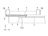
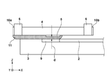
- the imprint apparatus 1 removes the auxiliary plate 9 disposed on the substrate stage 3 so as to surround the periphery of the substrate 2 and the mold 4. And a supply unit 60 for supplying the gas 11.
- the auxiliary plate 9 does not have to surround the substrate 2 and is a peripheral member disposed around the portion of the substrate stage where the substrate 2 is held. Further, the auxiliary plate 9 is configured such that the height of the surface of the auxiliary plate 9 and the height of the surface of the substrate 2 are substantially the same (the difference is 1 mm or less).
- the supply unit 60 includes a gas supply source 12, a first supply unit 10a, and a second supply unit 10b. As shown in FIGS.
- the first supply unit 10 a and the second supply unit 10 b transfer the gas 11 from the gas supply source 12 to the second space SP 2 adjacent to the first space SP 1 below the mold 4.
- the first space SP1 under the mold 4 is, for example, a space defined between the mold 4 and the substrate 2 when the mold 4 and the substrate 2 face each other.
- the space is defined between the mold 4 and the auxiliary plate 9.
- the first supply unit 10a and the dispenser 7 are arranged with the mold holding unit 6 interposed therebetween.
- maintenance part 6 do not need to be arrange
- the mold holding unit 6, and the dispenser 7 are arranged in this order with respect to the position in at least a predetermined direction (X-axis direction in the present embodiment), even if the position in the Y-axis direction is slightly shifted. Good.
- the second supply unit 10b is disposed between the dispenser 7 and the mold holding unit 6, and the first supply unit 10a and the second supply unit 10b are disposed with the mold holding unit 6 interposed therebetween.
- FIG. 2a shows the case where the mold 4 is charged to the plus side, but the material and shape of the mold 4, the substrate 2 and the imprint material 8, and when the mold 4 is pulled away from the cured imprint material 8 on the substrate.
- the mold 4 may be charged to the negative side depending on the above conditions.
- the dispenser 7 is used to supply the imprint material 8 to the second region (shot region) of the substrate 2. It is necessary to move the substrate stage 3 below.
- the supply of the gas 11 by the first supply unit 10a is started before the movement of the substrate stage 3 below the dispenser 7 is started. Accordingly, the gas 11 supplied from the first supply unit 10 a to the second space SP ⁇ b> 2 by the Couette flow generated on the surface of the substrate 2 and the substrate stage 3 due to the movement of the substrate stage 3 is the second under the mold 4. It is drawn into 1 space SP1.
- the gas 11 for static elimination needs to contain the gas whose mean free path with respect to an electron is longer than air.
- a rare gas that is a monoatomic molecule is preferable, but helium having the longest mean free path among the rare gases is particularly preferable.
- Electrons existing in the electric field are carried to the anode side by the electric field, and collide with gas molecules in the middle. At this time, if the electrons are sufficiently accelerated to collide with gas molecules having energy equal to or higher than the gas ionization voltage, ionization occurs and an electron-cation pair is generated. The electrons generated here are also accelerated by the electric field and ionize the gas molecules.
- an electron avalanche a phenomenon in which a large amount of electron-cation pairs is generated by successive ionization.
- a gas having a long mean free path for electrons is accelerated to a high energy state without causing electrons being accelerated to collide with gas molecules. Therefore, a gas having a long mean free path for electrons is more likely to cause an electron avalanche even in a low electric field than air, and can be discharged before a large voltage is accumulated in the mold 4.
- the auxiliary plate 9 facing the mold 4 has conductivity on the surface of the mold 4 side.
- the auxiliary plate 9 is made of metal.
- the imprint process in the imprint apparatus 1 will be described, particularly focusing on the charge removal of the mold 4.
- FIG. Such imprint processing is performed by the control unit 50 controlling the respective units of the imprint apparatus 1 in an integrated manner.
- the control unit 50 controlling the respective units of the imprint apparatus 1 in an integrated manner.
- a case where the pattern of the imprint material 8 is sequentially formed in each of the first region and the second region as the shot region of the substrate 2 will be described as an example.
- the substrate stage 3 holding the substrate 2 is moved to position the first region of the substrate 2 under the dispenser 7, and the imprint material 8 is supplied from the dispenser 7 to the first region of the substrate 2.
- the supply of the gas 11 by the supply unit 60 (the first supply unit 10a and the second supply unit 10b) is stopped.
- the supply of the gas 11 by the supply unit 60, specifically, the second supply unit 10b is started.
- the gas 11 is supplied only from the second supply unit 10b in order to suppress the usage amount of the gas 11.
- the second supply unit 10b may be supplied from the first supply unit 10a.
- the substrate stage 3 is moved to position the first region of the substrate 2 under the mold 4. At this time, the supply of the gas 11 by the second supply unit 10b is continued. Thereby, the gas 11 supplied from the second supply unit 10b to the second space SP2 is drawn into the first space SP1 below the mold 4, and the mold 4 and the substrate 2 (the imprint material 8 in the first region of the substrate 2). ) Can be filled with the gas 11.
- the mold 4 and the imprint material 8 in the first region of the substrate 2 are brought into contact with each other. While the mold 4 and the imprint material 8 are brought into contact with each other and the pattern portion 5 of the mold 4 is filled with the imprint material 8, the supply of the gas 11 by the second supply portion 10b is continued, The concentration of the gas 11 in the first space SP1 is set to 99% or more. Thereby, filling of the imprint material 8 to the pattern part 5 of the mold 4 can be promoted.
- the supply of the gas 11 by the second supply unit 10b is stopped before the imprint material 8 in the first region of the substrate 2 is cured while the mold 4 and the imprint material 8 are in contact with each other.
- the concentration of the gas 11 in the first space SP1 under the mold 4 is set to be less than 99%, more specifically 90% or less. That is, the ratio of oxygen around the mold 4 is increased as compared with the step of S308.
- the imprint material 8 attached to the side surface of the pattern portion 5 is cured in this way, the cured imprint material 8 is peeled off and becomes particles. Therefore, it is preferable that the imprint material 8 attached to the side surface of the pattern portion 5 is not cured, that is, left in an uncured state. Therefore, in the present embodiment, the concentration of the gas 11 in the first space SP1 under the mold 4 is increased to inhibit the curing reaction of the imprint material 8 by the ultraviolet rays 21 with oxygen.
- the uncured imprint material 8 attached to the side surface of the pattern portion 5 is a very small amount, it volatilizes by the time when the imprint material 8 supplied to the second region is cured. Accordingly, there is no influence on pattern formation in the second region.
- the gas 11 is supplied only from the first supply unit 10a in order to suppress the usage amount of the gas 11. However, if it is not necessary to suppress the usage amount of the gas 11, the first supply unit 10a. In addition, the gas 11 may be supplied from the second supply unit 10b.
- the mold 4 is pulled away from the cured imprint material 8 in the first region of the substrate 2. Thereby, the pattern of the imprint material 8 is formed in the first region of the substrate 2.
- the mold 4 (pattern part 5) is charged by pulling the mold 4 away from the cured imprint material 8 in the first region of the substrate 2. At this time, the supply of the gas 11 by the first supply unit 10a is continued.
- S317 it is determined whether or not the pattern of the imprint material 8 has been formed in all the shot areas of the substrate 2.
- the supply of the gas 11 by the first supply unit 10a is stopped and the operation is ended. If the pattern of the imprint material 8 is not formed in all shot areas of the substrate 2, the process proceeds to S318.
- the substrate stage 3 may be stopped in a state where the auxiliary plate 9 and the mold 4 face each other, or the substrate in a state where the auxiliary plate 9 and the mold 4 face each other.
- the speed of the stage 3 may be decreased.
- the second region of the substrate 2 is positioned below the dispenser. At this time, the supply of the gas 11 by the first supply unit 10a is stopped. In other words, when the substrate stage 3 reaches below the dispenser 7, the supply of the gas 11 by the first supply unit 10a is stopped. Then, the process proceeds to S ⁇ b> 302, where the imprint material 8 is supplied to the second region of the substrate 2, and the process for forming the pattern of the imprint material 8 in the second region of the substrate 2 is continued.
- the mold 4 is pulled away from the cured imprint material 8 in the first region of the substrate 2, it is below the dispenser 7 of the substrate stage 3 for supplying the imprint material 8 to the second region of the substrate 2.
- the supply of the gas 11 by the first supply unit 10a is started.
- the gas 11 supplied to the second space SP2 is sent to the first space SP1, and the auxiliary plate 9 is opposed to the mold 4 so that the mold 11 passes through the gas 11. 4 is removed.
- the mold 4 can be efficiently neutralized, so that the adhesion of foreign matters to the mold 4 is suppressed, the occurrence of defects in the pattern formed on the substrate, and the mold 4 breakage can be reduced.
- the gas 11 is supplied from the first supply unit 10a.
- the present invention is not limited to this.
- the supply of the gas 11 from the first supply unit 10a is not started, and the mold 4 is separated from the cured imprint material 8 on the substrate. After that, the supply of the gas 11 from the first supply unit 10a may be started.
- the auxiliary plate 9 may be electrically grounded.
- the potential of the mold 4 becomes the same as the potential of the auxiliary plate 9 that is grounded. Therefore, since the potential of the mold 4 is equal to that of the members inside the imprint apparatus 1, a strong electric field is not generated around the mold 4, and adhesion of foreign matters due to electrostatic force can be suppressed.
- the imprint apparatus 1 may further include an applying unit 70 that applies a potential to the auxiliary plate 9.
- the applying unit 70 reverses the polarity of the potential generated in the mold 4 by pulling the mold 4 away from the cured imprint material 8 on the substrate. Give the potential of the polarity.
- the potential difference between the mold 4 and the auxiliary plate 9 is widened, and the electric field between the mold 4 and the auxiliary plate 9 becomes strong, so that an electronic avalanche is likely to occur. Therefore, even when the charge amount of the mold 4 due to the peeling charge is small, the charge removal of the mold 4 by the electronic avalanche can be performed. As shown in FIG.
- the applying unit 70 includes a power source that can apply potentials of both poles to the auxiliary plate 9.
- the electronic avalanche that occurs between the mold 4 and the auxiliary plate 9 can be controlled by adjusting not only the type of the gas 11 but also the distance between the mold 4 and the auxiliary plate 9.
- the electric field strength between the mold 4 and the auxiliary plate 9 can be adjusted by adjusting the distance between the mold 4 and the auxiliary plate 9. Therefore, as shown in FIG. 6, when the auxiliary plate 9 is opposed to the mold 4, the distance d between the mold 4 and the auxiliary plate 9 is adjusted.
- the distance changing unit that changes the distance d between the mold 4 and the auxiliary plate 9 the mold holding unit 6 and the substrate stage 3 can be used.
- the electronic avalanche that occurs between the mold 4 and the auxiliary plate 9 can be controlled by adjusting the pressure in the space between the mold 4 and the auxiliary plate 9.
- the mean free path of electrons between the mold 4 and the auxiliary plate 9 can be adjusted by adjusting the pressure in the space between the mold 4 and the auxiliary plate 9. Therefore, when a pressure changing unit that changes the pressure in the space between the mold 4 and the auxiliary plate 9 is provided and the auxiliary plate 9 is opposed to the mold 4, the pressure changing unit causes the mold 4 and the auxiliary plate 9 to move. Adjust the space pressure between.
- the pressure changing unit may locally change the pressure in the space between the mold 4 and the auxiliary plate 9 or the pressure in the vicinity including the space, or the pressure in the entire space of the imprint apparatus 1. It may be changed.
- the imprint apparatus 1 may further include an energy irradiation unit 30 that irradiates the auxiliary plate 9 with light 31.
- the energy irradiating unit 30 irradiates the auxiliary plate 9 with light 31 having energy equal to or higher than the work function of the auxiliary plate 9.
- the work function of the auxiliary plate 9 is about 4 eV. Therefore, when the light 31 having a wavelength of 300 nm or less is irradiated, the auxiliary plate 9 (on the mold 4 side) is caused by the photoelectric effect. Photoelectrons are emitted from the surface.
- the work function of metal is generally about 2 eV to 5 eV
- photoelectrons are emitted from the auxiliary plate 9 by the photoelectric effect when the auxiliary plate 9 is irradiated with light 31 in the ultraviolet region. Since such photoelectrons are involved in an electron avalanche, the static elimination efficiency of the mold 4 can be further improved.
- the gas 11 for charge removal used in the imprint apparatus 1 is generally highly diffusible. Therefore, as described above, when the mold 4 and the imprint material 8 on the substrate are brought into contact with each other, the space between the mold 4 and the substrate 2 is filled with the gas 11, thereby imprinting on the pattern portion 5 of the mold 4.
- the filling property of the printing material 8 can be improved. For this reason, it is good to supply the gas 11 during the process of making the mold 4 and the imprint material 8 on a board
- the rare gas used as the gas 11 is expensive, the gas 11 is supplied during the process of completing the filling of the imprint material 8 into the pattern portion 5 of the mold 4 and curing the imprint material 8. It is good to stop.
- the pattern of the cured product formed using the imprint apparatus 1 is used permanently on at least a part of various articles, or temporarily used when manufacturing various articles.
- the article is an electric circuit element, an optical element, a MEMS, a recording element, a sensor, or a mold.
- the electric circuit element include volatile or nonvolatile semiconductor memories such as DRAM, SRAM, flash memory, and MRAM, and semiconductor elements such as LSI, CCD, image sensor, and FPGA.
- Examples of the mold include an imprint mold.
- the cured product pattern is used as it is as at least a part of the above-mentioned article, or temporarily used as a mask. After etching or ion implantation is performed in the substrate processing step, the mask is removed.
- a substrate 2 such as a silicon wafer on which a workpiece such as an insulator is formed is prepared, and then an imprint material 8 is applied to the surface of the workpiece by an inkjet method or the like. To do.
- a state in which the imprint material 8 in the form of a plurality of droplets is applied on the substrate is shown.
- the imprint mold 4 is opposed to the imprint material 8 on the substrate with the side on which the concavo-convex pattern is formed facing.
- the substrate 2 provided with the imprint material 8 and the mold 4 are brought into contact with each other, and pressure is applied.
- the imprint material 8 is filled in the gap between the mold 4 and the workpiece. In this state, when light is irradiated as energy for curing through the mold 4, the imprint material 8 is cured.
- a pattern of a cured product of the imprint material 8 is formed on the substrate.
- This cured product pattern has a shape in which the concave portion of the mold 4 corresponds to the convex portion of the cured product, and the convex portion of the mold 4 corresponds to the concave portion of the cured product. Has been transcribed.
- the pattern of the cured product when etching is performed using the pattern of the cured product as an anti-etching mask, a portion of the surface of the workpiece that has no cured product or remains thinly is removed to form a groove. As shown in FIG. 8f, when the cured product pattern is removed, an article having grooves formed on the surface of the workpiece can be obtained.
- the pattern of the cured product is removed, it may be used as, for example, an interlayer insulating film included in a semiconductor element, that is, a constituent member of an article without being removed after processing.
Landscapes
- Engineering & Computer Science (AREA)
- General Physics & Mathematics (AREA)
- Physics & Mathematics (AREA)
- Microelectronics & Electronic Packaging (AREA)
- Manufacturing & Machinery (AREA)
- Computer Hardware Design (AREA)
- Condensed Matter Physics & Semiconductors (AREA)
- Power Engineering (AREA)
- Mechanical Engineering (AREA)
- Health & Medical Sciences (AREA)
- Environmental & Geological Engineering (AREA)
- Epidemiology (AREA)
- Public Health (AREA)
- Shaping Of Tube Ends By Bending Or Straightening (AREA)
- Exposure Of Semiconductors, Excluding Electron Or Ion Beam Exposure (AREA)
Priority Applications (2)
| Application Number | Priority Date | Filing Date | Title |
|---|---|---|---|
| KR1020197016503A KR102179737B1 (ko) | 2016-11-18 | 2017-10-05 | 임프린트 장치, 임프린트 방법, 및 물품 제조 방법 |
| US16/408,586 US11333971B2 (en) | 2016-11-18 | 2019-05-10 | Imprint apparatus, imprint method, and method of manufacturing article |
Applications Claiming Priority (2)
| Application Number | Priority Date | Filing Date | Title |
|---|---|---|---|
| JP2016-225375 | 2016-11-18 | ||
| JP2016225375A JP6735656B2 (ja) | 2016-11-18 | 2016-11-18 | インプリント装置、インプリント方法及び物品の製造方法 |
Related Child Applications (1)
| Application Number | Title | Priority Date | Filing Date |
|---|---|---|---|
| US16/408,586 Continuation US11333971B2 (en) | 2016-11-18 | 2019-05-10 | Imprint apparatus, imprint method, and method of manufacturing article |
Publications (1)
| Publication Number | Publication Date |
|---|---|
| WO2018092454A1 true WO2018092454A1 (ja) | 2018-05-24 |
Family
ID=62146147
Family Applications (1)
| Application Number | Title | Priority Date | Filing Date |
|---|---|---|---|
| PCT/JP2017/036246 Ceased WO2018092454A1 (ja) | 2016-11-18 | 2017-10-05 | インプリント装置、インプリント方法及び物品の製造方法 |
Country Status (5)
| Country | Link |
|---|---|
| US (1) | US11333971B2 (enExample) |
| JP (1) | JP6735656B2 (enExample) |
| KR (1) | KR102179737B1 (enExample) |
| TW (1) | TWI661925B (enExample) |
| WO (1) | WO2018092454A1 (enExample) |
Cited By (1)
| Publication number | Priority date | Publication date | Assignee | Title |
|---|---|---|---|---|
| CN113448178A (zh) * | 2020-03-24 | 2021-09-28 | 株式会社斯库林集团 | 曝光装置 |
Families Citing this family (6)
| Publication number | Priority date | Publication date | Assignee | Title |
|---|---|---|---|---|
| JP7149872B2 (ja) * | 2019-02-14 | 2022-10-07 | キヤノン株式会社 | インプリント方法、インプリント装置、および物品の製造方法 |
| US11181819B2 (en) | 2019-05-31 | 2021-11-23 | Canon Kabushiki Kaisha | Frame curing method for extrusion control |
| US12353127B2 (en) * | 2021-04-14 | 2025-07-08 | Canon Kabushiki Kaisha | Imprint apparatus, imprint method and article manufacturing method |
| TWI837607B (zh) * | 2022-03-10 | 2024-04-01 | 永嘉光電股份有限公司 | 大規模壓印之方法 |
| JP7731831B2 (ja) | 2022-03-11 | 2025-09-01 | キオクシア株式会社 | インプリント方法、半導体装置の製造方法、及びインプリント装置 |
| US12463042B2 (en) * | 2022-05-31 | 2025-11-04 | Canon Kabushiki Kaisha | Planarization system and method |
Citations (4)
| Publication number | Priority date | Publication date | Assignee | Title |
|---|---|---|---|---|
| JP2008260273A (ja) * | 2007-03-16 | 2008-10-30 | Canon Inc | インプリント方法、チップの製造方法及びインプリント装置 |
| JP2014183069A (ja) * | 2013-03-18 | 2014-09-29 | Dainippon Printing Co Ltd | インプリント方法およびインプリント装置 |
| JP2015115413A (ja) * | 2013-12-10 | 2015-06-22 | キヤノン株式会社 | インプリント装置及び物品の製造方法 |
| JP2016031952A (ja) * | 2014-07-25 | 2016-03-07 | キヤノン株式会社 | インプリント装置及び物品の製造方法 |
Family Cites Families (10)
| Publication number | Priority date | Publication date | Assignee | Title |
|---|---|---|---|---|
| FR2133154A5 (enExample) | 1971-04-09 | 1972-11-24 | Cii | |
| JP2007098779A (ja) | 2005-10-05 | 2007-04-19 | Nikon Corp | 樹脂の剥離方法及びパターン転写装置 |
| JP5235506B2 (ja) | 2008-06-02 | 2013-07-10 | キヤノン株式会社 | パターン転写装置及びデバイス製造方法 |
| JP5868215B2 (ja) * | 2012-02-27 | 2016-02-24 | キヤノン株式会社 | インプリント装置およびインプリント方法、それを用いた物品の製造方法 |
| JP6661397B2 (ja) * | 2015-04-22 | 2020-03-11 | キヤノン株式会社 | インプリント装置、インプリント方法、および物品の製造方法 |
| JP6603678B2 (ja) * | 2016-02-26 | 2019-11-06 | キヤノン株式会社 | インプリント装置およびその動作方法ならびに物品製造方法 |
| JP6643145B2 (ja) * | 2016-02-29 | 2020-02-12 | キヤノン株式会社 | インプリント装置、モールド、インプリント方法及び物品の製造方法 |
| JP6732475B2 (ja) * | 2016-02-29 | 2020-07-29 | キヤノン株式会社 | インプリント装置、物品の製造方法、保持装置および露光装置 |
| JP6704769B2 (ja) * | 2016-03-29 | 2020-06-03 | キヤノン株式会社 | インプリント装置、および物品の製造方法 |
| US10754244B2 (en) * | 2016-03-31 | 2020-08-25 | Canon Kabushiki Kaisha | Pattern forming method as well as production methods for processed substrate, optical component, circuit board, electronic component and imprint mold |
-
2016
- 2016-11-18 JP JP2016225375A patent/JP6735656B2/ja active Active
-
2017
- 2017-10-05 KR KR1020197016503A patent/KR102179737B1/ko active Active
- 2017-10-05 WO PCT/JP2017/036246 patent/WO2018092454A1/ja not_active Ceased
- 2017-10-18 TW TW106135607A patent/TWI661925B/zh active
-
2019
- 2019-05-10 US US16/408,586 patent/US11333971B2/en active Active
Patent Citations (4)
| Publication number | Priority date | Publication date | Assignee | Title |
|---|---|---|---|---|
| JP2008260273A (ja) * | 2007-03-16 | 2008-10-30 | Canon Inc | インプリント方法、チップの製造方法及びインプリント装置 |
| JP2014183069A (ja) * | 2013-03-18 | 2014-09-29 | Dainippon Printing Co Ltd | インプリント方法およびインプリント装置 |
| JP2015115413A (ja) * | 2013-12-10 | 2015-06-22 | キヤノン株式会社 | インプリント装置及び物品の製造方法 |
| JP2016031952A (ja) * | 2014-07-25 | 2016-03-07 | キヤノン株式会社 | インプリント装置及び物品の製造方法 |
Cited By (1)
| Publication number | Priority date | Publication date | Assignee | Title |
|---|---|---|---|---|
| CN113448178A (zh) * | 2020-03-24 | 2021-09-28 | 株式会社斯库林集团 | 曝光装置 |
Also Published As
| Publication number | Publication date |
|---|---|
| KR102179737B1 (ko) | 2020-11-17 |
| JP6735656B2 (ja) | 2020-08-05 |
| TWI661925B (zh) | 2019-06-11 |
| US20190265589A1 (en) | 2019-08-29 |
| JP2018082127A (ja) | 2018-05-24 |
| US11333971B2 (en) | 2022-05-17 |
| TW201819153A (zh) | 2018-06-01 |
| KR20190073573A (ko) | 2019-06-26 |
Similar Documents
| Publication | Publication Date | Title |
|---|---|---|
| US11333971B2 (en) | Imprint apparatus, imprint method, and method of manufacturing article | |
| JP6603678B2 (ja) | インプリント装置およびその動作方法ならびに物品製造方法 | |
| JP7261000B2 (ja) | 容器、処理装置、異物除去方法、および物品の製造方法 | |
| TWI649183B (zh) | 壓印裝置,壓印方法,及製造物品的方法 | |
| US10131134B2 (en) | System and method for discharging electrostatic charge in nanoimprint lithography processes | |
| JP2017139452A (ja) | インプリント装置および物品の製造方法 | |
| WO2016170729A1 (en) | Imprint apparatus, method of imprinting, and method of manufacturing article | |
| US10777443B2 (en) | Imprint apparatus, imprinting method, and method for manufacturing article | |
| KR102294037B1 (ko) | 임프린트 장치, 및 물품 제조 방법 | |
| JP6704769B2 (ja) | インプリント装置、および物品の製造方法 | |
| KR102461027B1 (ko) | 몰드를 사용해서 기판 상의 조성물을 성형하는 성형 장치, 및 물품 제조 방법 | |
| US12453991B2 (en) | Foreign particle removing method, formation method, article manufacturing method, foreign particle removing apparatus, and system | |
| JP2020013890A (ja) | インプリント装置およびその制御方法、ならびに物品製造方法 | |
| JP2019067916A (ja) | リソグラフィ装置、および物品の製造方法 | |
| JP2019091741A (ja) | インプリント装置、インプリント方法、および物品の製造方法 | |
| WO2017145924A1 (ja) | インプリント装置およびその動作方法ならびに物品製造方法 | |
| JP2017157640A (ja) | インプリント装置、物品の製造方法、保持装置および露光装置 | |
| JP2025095925A (ja) | 平坦化装置、および物品製造方法 | |
| JP6948924B2 (ja) | インプリント装置、インプリント方法、および物品製造方法 | |
| US10303049B2 (en) | Reducing electric charge in imprint lithography | |
| JP2019117845A (ja) | リソグラフィ装置及び物品の製造方法 | |
| WO2017134989A1 (ja) | インプリント装置および物品の製造方法 | |
| JP2018190802A (ja) | インプリント装置および物品の製造方法 |
Legal Events
| Date | Code | Title | Description |
|---|---|---|---|
| 121 | Ep: the epo has been informed by wipo that ep was designated in this application |
Ref document number: 17870911 Country of ref document: EP Kind code of ref document: A1 |
|
| NENP | Non-entry into the national phase |
Ref country code: DE |
|
| ENP | Entry into the national phase |
Ref document number: 20197016503 Country of ref document: KR Kind code of ref document: A |
|
| 122 | Ep: pct application non-entry in european phase |
Ref document number: 17870911 Country of ref document: EP Kind code of ref document: A1 |