WO2018088071A1 - 現像装置、基板処理装置、現像方法および基板処理方法 - Google Patents
現像装置、基板処理装置、現像方法および基板処理方法 Download PDFInfo
- Publication number
- WO2018088071A1 WO2018088071A1 PCT/JP2017/036073 JP2017036073W WO2018088071A1 WO 2018088071 A1 WO2018088071 A1 WO 2018088071A1 JP 2017036073 W JP2017036073 W JP 2017036073W WO 2018088071 A1 WO2018088071 A1 WO 2018088071A1
- Authority
- WO
- WIPO (PCT)
- Prior art keywords
- coating film
- metal
- substrate
- pattern
- organic
- Prior art date
- Legal status (The legal status is an assumption and is not a legal conclusion. Google has not performed a legal analysis and makes no representation as to the accuracy of the status listed.)
- Ceased
Links
Images



Classifications
-
- G—PHYSICS
- G03—PHOTOGRAPHY; CINEMATOGRAPHY; ANALOGOUS TECHNIQUES USING WAVES OTHER THAN OPTICAL WAVES; ELECTROGRAPHY; HOLOGRAPHY
- G03F—PHOTOMECHANICAL PRODUCTION OF TEXTURED OR PATTERNED SURFACES, e.g. FOR PRINTING, FOR PROCESSING OF SEMICONDUCTOR DEVICES; MATERIALS THEREFOR; ORIGINALS THEREFOR; APPARATUS SPECIALLY ADAPTED THEREFOR
- G03F7/00—Photomechanical, e.g. photolithographic, production of textured or patterned surfaces, e.g. printing surfaces; Materials therefor, e.g. comprising photoresists; Apparatus specially adapted therefor
- G03F7/26—Processing photosensitive materials; Apparatus therefor
- G03F7/30—Imagewise removal using liquid means
-
- G—PHYSICS
- G03—PHOTOGRAPHY; CINEMATOGRAPHY; ANALOGOUS TECHNIQUES USING WAVES OTHER THAN OPTICAL WAVES; ELECTROGRAPHY; HOLOGRAPHY
- G03F—PHOTOMECHANICAL PRODUCTION OF TEXTURED OR PATTERNED SURFACES, e.g. FOR PRINTING, FOR PROCESSING OF SEMICONDUCTOR DEVICES; MATERIALS THEREFOR; ORIGINALS THEREFOR; APPARATUS SPECIALLY ADAPTED THEREFOR
- G03F7/00—Photomechanical, e.g. photolithographic, production of textured or patterned surfaces, e.g. printing surfaces; Materials therefor, e.g. comprising photoresists; Apparatus specially adapted therefor
- G03F7/004—Photosensitive materials
-
- G—PHYSICS
- G03—PHOTOGRAPHY; CINEMATOGRAPHY; ANALOGOUS TECHNIQUES USING WAVES OTHER THAN OPTICAL WAVES; ELECTROGRAPHY; HOLOGRAPHY
- G03F—PHOTOMECHANICAL PRODUCTION OF TEXTURED OR PATTERNED SURFACES, e.g. FOR PRINTING, FOR PROCESSING OF SEMICONDUCTOR DEVICES; MATERIALS THEREFOR; ORIGINALS THEREFOR; APPARATUS SPECIALLY ADAPTED THEREFOR
- G03F7/00—Photomechanical, e.g. photolithographic, production of textured or patterned surfaces, e.g. printing surfaces; Materials therefor, e.g. comprising photoresists; Apparatus specially adapted therefor
- G03F7/16—Coating processes; Apparatus therefor
- G03F7/162—Coating on a rotating support, e.g. using a whirler or a spinner
-
- G—PHYSICS
- G03—PHOTOGRAPHY; CINEMATOGRAPHY; ANALOGOUS TECHNIQUES USING WAVES OTHER THAN OPTICAL WAVES; ELECTROGRAPHY; HOLOGRAPHY
- G03F—PHOTOMECHANICAL PRODUCTION OF TEXTURED OR PATTERNED SURFACES, e.g. FOR PRINTING, FOR PROCESSING OF SEMICONDUCTOR DEVICES; MATERIALS THEREFOR; ORIGINALS THEREFOR; APPARATUS SPECIALLY ADAPTED THEREFOR
- G03F7/00—Photomechanical, e.g. photolithographic, production of textured or patterned surfaces, e.g. printing surfaces; Materials therefor, e.g. comprising photoresists; Apparatus specially adapted therefor
- G03F7/20—Exposure; Apparatus therefor
-
- G—PHYSICS
- G03—PHOTOGRAPHY; CINEMATOGRAPHY; ANALOGOUS TECHNIQUES USING WAVES OTHER THAN OPTICAL WAVES; ELECTROGRAPHY; HOLOGRAPHY
- G03F—PHOTOMECHANICAL PRODUCTION OF TEXTURED OR PATTERNED SURFACES, e.g. FOR PRINTING, FOR PROCESSING OF SEMICONDUCTOR DEVICES; MATERIALS THEREFOR; ORIGINALS THEREFOR; APPARATUS SPECIALLY ADAPTED THEREFOR
- G03F7/00—Photomechanical, e.g. photolithographic, production of textured or patterned surfaces, e.g. printing surfaces; Materials therefor, e.g. comprising photoresists; Apparatus specially adapted therefor
- G03F7/26—Processing photosensitive materials; Apparatus therefor
- G03F7/30—Imagewise removal using liquid means
- G03F7/32—Liquid compositions therefor, e.g. developers
-
- G—PHYSICS
- G03—PHOTOGRAPHY; CINEMATOGRAPHY; ANALOGOUS TECHNIQUES USING WAVES OTHER THAN OPTICAL WAVES; ELECTROGRAPHY; HOLOGRAPHY
- G03F—PHOTOMECHANICAL PRODUCTION OF TEXTURED OR PATTERNED SURFACES, e.g. FOR PRINTING, FOR PROCESSING OF SEMICONDUCTOR DEVICES; MATERIALS THEREFOR; ORIGINALS THEREFOR; APPARATUS SPECIALLY ADAPTED THEREFOR
- G03F7/00—Photomechanical, e.g. photolithographic, production of textured or patterned surfaces, e.g. printing surfaces; Materials therefor, e.g. comprising photoresists; Apparatus specially adapted therefor
- G03F7/26—Processing photosensitive materials; Apparatus therefor
- G03F7/40—Treatment after imagewise removal, e.g. baking
-
- H—ELECTRICITY
- H10—SEMICONDUCTOR DEVICES; ELECTRIC SOLID-STATE DEVICES NOT OTHERWISE PROVIDED FOR
- H10P—GENERIC PROCESSES OR APPARATUS FOR THE MANUFACTURE OR TREATMENT OF DEVICES COVERED BY CLASS H10
- H10P14/00—Formation of materials, e.g. in the shape of layers or pillars
- H10P14/60—Formation of materials, e.g. in the shape of layers or pillars of insulating materials
- H10P14/63—Formation of materials, e.g. in the shape of layers or pillars of insulating materials characterised by the formation processes
- H10P14/6326—Deposition processes
- H10P14/6342—Liquid deposition, e.g. spin-coating, sol-gel techniques or spray coating
-
- H—ELECTRICITY
- H10—SEMICONDUCTOR DEVICES; ELECTRIC SOLID-STATE DEVICES NOT OTHERWISE PROVIDED FOR
- H10P—GENERIC PROCESSES OR APPARATUS FOR THE MANUFACTURE OR TREATMENT OF DEVICES COVERED BY CLASS H10
- H10P70/00—Cleaning of wafers, substrates or parts of devices
- H10P70/10—Cleaning before device manufacture, i.e. Begin-Of-Line process
- H10P70/15—Cleaning before device manufacture, i.e. Begin-Of-Line process by wet cleaning only
-
- H—ELECTRICITY
- H10—SEMICONDUCTOR DEVICES; ELECTRIC SOLID-STATE DEVICES NOT OTHERWISE PROVIDED FOR
- H10P—GENERIC PROCESSES OR APPARATUS FOR THE MANUFACTURE OR TREATMENT OF DEVICES COVERED BY CLASS H10
- H10P76/00—Manufacture or treatment of masks on semiconductor bodies, e.g. by lithography or photolithography
Definitions
- the present invention relates to a developing device for developing a substrate, a substrate processing apparatus, a developing method, and a substrate processing method.
- a coating film is formed by supplying a coating solution such as a resist solution onto a substrate.
- the coating film is exposed and then developed to form a predetermined pattern on the coating film.
- the substrate after the pattern is formed on the coating film is rinsed.
- the pattern collapse may occur due to the surface tension of the rinsing liquid in the rinsing process (see, for example, Patent Documents 1 and 2).
- Japanese Patent Application Laid-Open No. H10-228667 describes that pattern collapse is prevented by mixing isopropyl alcohol in the rinsing liquid and reducing the surface tension of the rinsing liquid.
- Citation 2 describes that after rinsing, the pattern is prevented from collapsing by replacing a fluorinated inert liquid having a specific gravity of 1.5 or more and a surface tension of dyns / cm or less with a rinsing liquid.
- An object of the present invention is to provide a developing device, a substrate processing apparatus, a developing method, and a substrate processing method capable of preventing the pattern of a coating film from collapsing.
- a developing device is a developing device that performs development processing on a substrate, and a metal-containing coating solution film is formed on one surface of the substrate as a metal-containing coating film.
- a first organic coating film formed of a photosensitive organic material and exposed in a predetermined pattern is formed on the containing coating film, and the developing device supplies a developer to the first organic coating film to thereby generate a predetermined film.
- a first removal liquid supply unit that forms a metal-containing coating film pattern having a pattern of: a rinsing liquid supply unit that supplies a rinsing liquid to a substrate having the first organic coating film pattern and the metal-containing coating film pattern .
- a metal-containing coating film is formed on one surface of the substrate, a first organic coating film is formed on the metal-containing coating film with a photosensitive organic material, and the first organic coating film is exposed to a predetermined pattern.
- the developer is supplied to the first organic coating film by the developer supply unit.
- the first organic coating film is developed, and a first organic coating film pattern having a predetermined pattern is formed.
- the first removal liquid is supplied to the first organic coating film pattern and the metal-containing coating film by the first removal liquid supply unit.
- the rinse liquid is supplied to the substrate having the first organic coating film pattern and the metal-containing coating film pattern by the rinse liquid supply unit.
- the substrate on which the first organic coating film pattern and the metal-containing coating film pattern are formed can be cleaned with the rinse liquid.
- the bonding force of the metal-containing coating film pattern to the substrate is larger than the bonding force of the first organic coating film pattern to the substrate. Therefore, even when a larger surface tension is applied, the metal-containing coating film pattern can remain without collapsing. Therefore, even when the first organic coating film pattern collapses due to the surface tension of the rinsing liquid in the above cleaning, the metal-containing coating film pattern can be prevented from collapsing.
- the first removal liquid may include an aqueous solution to which a chelating agent is added, an alkaline aqueous solution, or an acidic aqueous solution.
- the metal-containing coating film portion can be easily removed.
- the chelating agent is selected from the group consisting of organic acids, organic acid salts, amino acids, amino acid derivatives, inorganic alkalis, inorganic alkali salts, alkylamines, alkylamine derivatives, alkanolamines and alkanolamine derivatives. One kind or plural kinds may be included. In this case, the metal-containing coating film portion can be removed more easily.
- a developing device is a developing device that performs development processing on a substrate, and a film of a coating solution containing metal is formed as a metal-containing coating film on one surface of the substrate, A first organic coating film formed of a photosensitive organic material and exposed in a predetermined pattern is formed on the metal-containing coating film, and the developing device uses a first removal liquid for removing the metal as the first removal liquid.
- a first removal liquid supply unit for forming a first organic coating film pattern having a predetermined pattern and a metal-containing coating film pattern having a predetermined pattern by supplying the organic coating film and the metal-containing coating film to A rinsing liquid supply unit configured to supply a rinsing liquid to a substrate having one organic coating film pattern and a metal-containing coating film pattern.
- a metal-containing coating film is formed on one surface of the substrate, a first organic coating film is formed on the metal-containing coating film with a photosensitive organic material, and the first organic coating film is exposed to a predetermined pattern.
- the first removal liquid supply unit supplies the first removal liquid to the first organic coating film and the metal-containing coating film.
- the first organic coating film is developed, and a first organic coating film pattern having a predetermined pattern is formed.
- the portion of the metal-containing coating film exposed from the first organic coating film pattern is removed, and a metal-containing coating film pattern having a predetermined pattern is formed.
- the rinse liquid is supplied to the substrate having the first organic coating film pattern and the metal-containing coating film pattern by the rinse liquid supply unit.
- the substrate on which the first organic coating film pattern and the metal-containing coating film pattern are formed can be cleaned with the rinse liquid.
- the bonding force of the metal-containing coating film pattern to the substrate is larger than the bonding force of the first organic coating film pattern to the substrate. Therefore, even when a larger surface tension is applied, the metal-containing coating film pattern can remain without collapsing. Therefore, even when the first organic coating film pattern collapses due to the surface tension of the rinsing liquid in the above cleaning, the metal-containing coating film pattern can be prevented from collapsing.
- the first removal liquid may include an alkaline aqueous solution.
- the portion of the metal-containing coating film can be easily removed while developing the first organic coating film.
- the developing device may further include a rotation holding unit that holds the substrate and rotates the substrate after the rinse liquid is supplied by the rinse liquid supply unit.
- the substrate supplied with the rinse liquid can be dried in a short time.
- the bonding force between the metal-containing coating film pattern and the substrate is large, even when a centrifugal force is applied to the metal-containing coating film pattern due to the rotation of the substrate, the metal-containing coating film pattern can be prevented from collapsing. it can.
- the developing device applies the first organic coating film pattern to the substrate after the first removal liquid is supplied by the first removal liquid supply unit and before the rinse liquid is supplied by the rinse liquid supply unit. You may further provide the 2nd removal liquid supply part which supplies the 2nd removal liquid for removing. In this case, the first organic coating film pattern which becomes unnecessary after the metal-containing coating film pattern is formed can be removed with a simple configuration.
- a second organic coating film may be further formed on the substrate between the one surface and the metal-containing coating film.
- by forming the second organic coating film thick it is possible to form a pattern of the second organic coating film having a large thickness and a small width.
- the developing device removes the second organic coating film on the substrate after the first removing liquid is supplied by the first removing liquid supply unit and before the rinsing liquid is supplied by the rinsing liquid supply unit.
- a third removal liquid supply unit that forms a second organic coating film pattern having a predetermined pattern by supplying a third removal liquid for the purpose may be further provided.
- the portion of the second organic coating film exposed from the metal-containing coating film pattern is removed by the third removal liquid.
- the 2nd organic coating film pattern which has a predetermined pattern can be formed easily.
- a substrate processing apparatus is a substrate processing apparatus disposed so as to be adjacent to an exposure apparatus that exposes a substrate, wherein the substrate contains a metal-containing coating solution as a metal-containing coating solution.
- a metal-containing coating film forming portion that forms a metal-containing coating film on one surface by supplying to one surface, and a metal-containing coating film by supplying a first organic coating liquid formed of a photosensitive material to the metal-containing coating film
- a developing device according to one aspect or another aspect of the present invention, which performs development processing on a substrate whose film is exposed to a predetermined pattern by an exposure device.
- the metal-containing coating solution is supplied to one surface of the substrate by the metal-containing coating film forming unit. Thereby, a metal-containing coating film is formed on one surface of the substrate.
- a first organic coating solution formed of a photosensitive material is supplied to the metal-containing coating film by the first organic coating film forming unit. Thereby, a 1st organic coating film is formed on the metal containing coating film formed of the metal containing coating film formation part.
- the first organic coating film formed by the first organic coating film forming unit is exposed to a predetermined pattern.
- the developer is supplied to the first organic coating film exposed in a predetermined pattern by the developer supply unit. Thereby, the first organic coating film is developed, and a first organic coating film pattern having a predetermined pattern is formed.
- the first removal liquid is supplied to the first organic coating film pattern and the metal-containing coating film by the first removal liquid supply unit. Thereby, the part of the metal-containing coating film exposed from the first organic coating film pattern is removed, and a metal-containing coating film pattern having a predetermined pattern is formed. Thereafter, the rinse liquid is supplied to the substrate having the first organic coating film pattern and the metal-containing coating film pattern by the rinse liquid supply unit.
- the substrate on which the first organic coating film pattern and the metal-containing coating film pattern are formed can be cleaned with the rinse liquid.
- the bonding force of the metal-containing coating film pattern to the substrate is larger than the bonding force of the first organic coating film pattern to the substrate. Therefore, even when a larger surface tension is applied, the metal-containing coating film pattern can remain without collapsing. Therefore, even when the first organic coating film pattern collapses due to the surface tension of the rinsing liquid in the above cleaning, the metal-containing coating film pattern can be prevented from collapsing.
- the substrate processing apparatus supplies the second organic coating solution to one surface of the substrate before the metal-containing coating film is formed on the one surface by the metal-containing coating film forming unit. You may further provide the 2nd organic coating film formation part which forms a 2nd organic coating film between films
- a second organic coating film is formed between one surface of the substrate and the metal-containing coating film.
- the second organic coating film can be formed into a predetermined pattern using the metal-containing coating film pattern. Further, by forming the second organic coating film thick, it is possible to form a pattern of the second organic coating film having a large thickness and a small width.
- a developing method is a developing method for performing development processing on a substrate, and a film of a coating solution containing a metal is formed on one surface of the substrate as a metal-containing coating film.
- a first organic coating film formed of a photosensitive organic material and exposed in a predetermined pattern is formed on the metal-containing coating film, and the developing method uses the developer supply unit to apply the first organic coating film.
- a metal-containing coating film is formed on one surface of the substrate, a first organic coating film is formed on the metal-containing coating film with a photosensitive organic material, and the first organic coating film is exposed to a predetermined pattern.
- the developer is supplied to the first organic coating film by the developer supply unit.
- the first organic coating film is developed, and a first organic coating film pattern having a predetermined pattern is formed.
- the first removal liquid is supplied to the first organic coating film pattern and the metal-containing coating film by the first removal liquid supply unit.
- the rinse liquid is supplied to the substrate having the first organic coating film pattern and the metal-containing coating film pattern by the rinse liquid supply unit.
- the substrate on which the first organic coating film pattern and the metal-containing coating film pattern are formed can be washed with the rinse liquid.
- the bonding force of the metal-containing coating film pattern to the substrate is larger than the bonding force of the first organic coating film pattern to the substrate. Therefore, even when a larger surface tension is applied, the metal-containing coating film pattern can remain without collapsing. Therefore, even when the first organic coating film pattern collapses due to the surface tension of the rinsing liquid in the above cleaning, the metal-containing coating film pattern can be prevented from collapsing.
- a development method is a development method for performing development processing on a substrate, and a film of a coating solution containing a metal is formed on one surface of the substrate as a metal-containing coating film.
- a first organic coating film formed of a photosensitive organic material and exposed in a predetermined pattern is formed on the metal-containing coating film, and the development method uses a first removal liquid for removing the metal Step of forming a first organic coating film pattern having a predetermined pattern and a metal-containing coating film pattern having a predetermined pattern by supplying the first organic coating film and the metal-containing coating film by one removing liquid supply unit And supplying a rinsing liquid to the substrate having the first organic coating film pattern and the metal-containing coating film pattern by the rinsing liquid supply unit.
- a metal-containing coating film is formed on one surface of the substrate, a first organic coating film is formed on the metal-containing coating film with a photosensitive organic material, and the first organic coating film is exposed to a predetermined pattern.
- the first removal liquid is supplied to the first organic coating film and the metal-containing coating film by the first removal liquid supply unit.
- the first organic coating film is developed, and a first organic coating film pattern having a predetermined pattern is formed.
- the portion of the metal-containing coating film exposed from the first organic coating film pattern is removed, and a metal-containing coating film pattern having a predetermined pattern is formed.
- the rinse liquid is supplied to the substrate having the first organic coating film pattern and the metal-containing coating film pattern by the rinse liquid supply unit.
- the substrate on which the first organic coating film pattern and the metal-containing coating film pattern are formed can be washed with the rinse liquid.
- the bonding force of the metal-containing coating film pattern to the substrate is larger than the bonding force of the first organic coating film pattern to the substrate. Therefore, even when a larger surface tension is applied, the metal-containing coating film pattern can remain without collapsing. Therefore, even when the first organic coating film pattern collapses due to the surface tension of the rinsing liquid in the above cleaning, the metal-containing coating film pattern can be prevented from collapsing.
- the developing method may further include a step of holding and rotating the substrate after the rinsing liquid is supplied by the rinsing liquid supply unit by the rotation holding unit.
- the substrate supplied with the rinse liquid can be dried in a short time.
- the bonding force between the metal-containing coating film pattern and the substrate is large, even when a centrifugal force is applied to the metal-containing coating film pattern due to the rotation of the substrate, the metal-containing coating film pattern can be prevented from collapsing. it can.
- a substrate processing method is a substrate processing method using an exposure apparatus that exposes a substrate, wherein a metal-containing coating liquid is used as a metal-containing coating film forming portion. Forming a metal-containing coating film on one surface by supplying to one surface of the substrate, and forming a metal-containing coating film by forming a first organic coating liquid formed of a photosensitive material by a first organic coating film forming unit.
- the metal-containing coating solution is supplied to one surface of the substrate by the metal-containing coating film forming unit. Thereby, a metal-containing coating film is formed on one surface of the substrate.
- a first organic coating solution formed of a photosensitive material is supplied to the metal-containing coating film by the first organic coating film forming unit. Thereby, a 1st organic coating film is formed on the metal containing coating film formed of the metal containing coating film formation part.
- the first organic coating film formed by the first organic coating film forming unit is exposed to a predetermined pattern.
- the developer is supplied to the first organic coating film exposed to a predetermined pattern by the developer supply unit.
- the first organic coating film is developed, and a first organic coating film pattern having a predetermined pattern is formed.
- the first removal liquid is supplied to the first organic coating film pattern and the metal-containing coating film by the first removal liquid supply unit.
- the rinse liquid is supplied to the substrate having the first organic coating film pattern and the metal-containing coating film pattern by the rinse liquid supply unit.
- the substrate on which the first organic coating film pattern and the metal-containing coating film pattern are formed can be washed with the rinse liquid.
- the bonding force of the metal-containing coating film pattern to the substrate is larger than the bonding force of the first organic coating film pattern to the substrate. Therefore, even when a larger surface tension is applied, the metal-containing coating film pattern can remain without collapsing. Therefore, even when the first organic coating film pattern collapses due to the surface tension of the rinsing liquid in the above cleaning, the metal-containing coating film pattern can be prevented from collapsing.
- the second organic coating liquid is supplied to one surface of the substrate by the second organic coating film forming unit, so that the one surface and the metal-containing coating film are provided.
- a step of forming a second organic coating film between the two may be further included.
- a second organic coating film is formed between one surface of the substrate and the metal-containing coating film.
- the second organic coating film can be formed into a predetermined pattern using the metal-containing coating film pattern. Further, by forming the second organic coating film thick, it is possible to form a pattern of the second organic coating film having a large thickness and a small width.
- the collapse of the coating film pattern can be prevented.
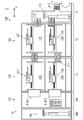
- FIG. 1 is a schematic plan view showing a configuration of a development processing unit according to an embodiment of the present invention.
- FIG. 2 is a partially enlarged longitudinal sectional view of a substrate to be processed by the development processing unit of FIG.
- FIG. 3 is a diagram for explaining the operation of the development processing unit of FIG.
- FIG. 4 is a diagram for explaining the operation of the development processing unit of FIG.
- FIG. 5 is a schematic plan view of a substrate processing apparatus including the development processing unit of FIG.
- FIG. 6 is a schematic side view showing the internal configuration of the coating processing section, coating development processing section and cleaning / drying processing section of FIG.
- FIG. 7 is a schematic side view showing the internal configuration of the heat treatment section and the cleaning / drying processing section of FIG.
- FIG. 8 is a schematic side view showing the internal configuration of the transport unit.
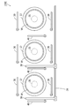
- FIG. 9 is a schematic plan view showing a configuration of a development processing unit according to another embodiment.
- FIG. 10 is a diagram for explaining the operation of the development processing
- a substrate means a semiconductor substrate, a liquid crystal display device or an FPD (Flat Panel Display) substrate such as an organic EL (Electro Luminescence) display device, an optical disk substrate, a magnetic disk substrate, or a magneto-optical disk. It refers to a substrate, a photomask substrate, a solar cell substrate, or the like.
- FIG. 1 is a schematic plan view showing the configuration of a development processing unit according to an embodiment of the present invention.
- the development processing unit (spin developer) 139 includes a plurality of replacement nozzles 30, a plurality of spin chucks 35, a plurality of rinse nozzles 36, and a plurality of cups 37.
- the development processing unit 139 also includes two slit nozzles 38 that discharge the developer and a moving mechanism 39 that moves the slit nozzles 38 in one direction.
- three replacement nozzles 30, spin chucks 35, rinse nozzles 36, and cups 37 are provided in the development processing unit 139.
- Each spin chuck 35 is rotationally driven by a driving device (not shown) (for example, an electric motor) while holding the substrate W.
- the cup 37 is provided so as to surround the periphery of the spin chuck 35.
- a developer is supplied to each slit nozzle 38 from a developer reservoir (not shown) through a developer pipe.
- One of the slit nozzles 38 is moved above the substrate W by the moving mechanism 39.
- the developing solution is discharged from the slit nozzle 38 while the spin chuck 35 rotates, whereby the development processing of the substrate W is performed.
- the replacement nozzle 30 is provided so as to be rotatable between a retracted position outside the cup 37 and a processing position above the center of the substrate W held by the spin chuck 35. At the time of replacement processing after the development processing of the substrate W, the replacement nozzle 30 is moved to the processing position. The replacement process of the substrate W is performed by discharging the replacement liquid from the replacement nozzle 30 while the spin chuck 35 rotates.
- the replacement liquid for example, an alkaline replacement liquid or an acidic replacement liquid is used.
- the alkaline replacement liquid is an aqueous solution containing, for example, ammonia and hydrogen peroxide.
- the alkaline substitution liquid may be, for example, TMAH (tetramethylammonium hydroxide).
- the acidic replacement liquid is an aqueous solution containing dilute hydrofluoric acid, for example.
- the acidic substitution liquid may be an aqueous solution containing, for example, sulfuric acid and hydrogen peroxide, or an aqueous solution containing acetic acid.
- the replacement liquid may be an aqueous solution containing a chelating agent.
- the chelating agent is an organic acid, an organic acid salt, an amino acid, an amino acid derivative, an inorganic alkali, an inorganic alkali salt, an alkylamine, an alkylamine derivative, an alkanolamine, and an alkanolamine derivative. Including multiple species.
- the rinse nozzle 36 is provided so as to be rotatable between a retracted position outside the cup 37 and a processing position above the center of the substrate W held by the spin chuck 35. During the rinsing process after the replacement process of the substrate W, the rinsing nozzle 36 is moved to the processing position. The rinse treatment of the substrate W is performed by discharging the rinse liquid from the rinse nozzle 36 while the spin chuck 35 rotates.
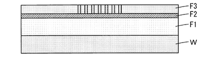
- FIG. 2 is a partially enlarged longitudinal sectional view of the substrate W to be processed by the development processing unit 139 in FIG.
- three types of coating films F1, F2, and F3 are formed on the surface to be processed of the substrate W as resist films.
- the coating film F1 is formed on the surface to be processed of the substrate W
- the coating film F2 is formed on the coating film F1
- the coating film F3 is formed on the coating film F2.
- the coating films F1 to F3 are formed on the target surface of the substrate W by the substrate processing apparatus 100 shown in FIGS.
- the coating film F1 is a non-photosensitive organic film, and is an SOC (Spin-On-Carbon) film in this example.
- the coating film F1 is referred to as an organic coating film F1.
- the organic coating film F1 has a relatively large thickness. In this example, the thickness of the organic coating film F1 is, for example, not less than 100 nm and not more than 300 nm.
- the coating film F2 is a non-photosensitive inorganic film.
- the coating film F2 contains a metal component such as a metal component or a metal oxide as a composition.
- a metal component such as a metal component or a metal oxide as a composition.
- Sn (tin), HfO 2 (hafnium oxide) or ZrO 2 (zirconium dioxide) is contained in the coating film F2 as the metal component.
- the coating film F2 is referred to as a metal-containing coating film F2.
- the metal-containing coating film F2 has a relatively small thickness. In this example, the thickness of the metal-containing coating film F2 is, for example, 5 nm or more and 30 nm or less.
- the coating film F3 is an organic film having photosensitivity in the ultraviolet region, for example.
- the coating film F3 is referred to as an organic coating film F3.
- the organic coating film F3 is exposed in a predetermined pattern.
- the thickness of the organic coating film F3 is, for example, 20 nm or more and 60 nm or less.
- the organic coating film F1 and the metal-containing coating film F2 are non-photosensitive, but the present invention is not limited to this.
- the photosensitive wavelength region is different from the organic coating film F3, the organic coating film F1 and the metal-containing coating film F2 may have photosensitivity.
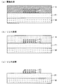
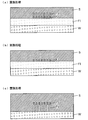
- FIG. 3 and 4 are diagrams for explaining the operation of the development processing unit 139 in FIG.
- the developer 1 is supplied to the substrate W from the slit nozzle 38 (FIG. 1).
- a liquid layer of the developer 1 is formed on the surface to be processed of the substrate W.
- the rinse liquid 2 is supplied to the substrate W from the rinse nozzle 36 (FIG. 1).
- unnecessary portions of the organic coating film F3 and the developer 1 are removed, and a pattern is formed in the organic coating film F3.
- the replacement liquid 3 is supplied from the replacement nozzle 30 (FIG. 1) to the substrate W as shown in FIG.
- a liquid layer of the replacement liquid 3 is formed on the surface to be processed of the substrate W, and the rinsing liquid 2 remaining on the surface to be processed of the substrate W is replaced with the replacement liquid 3.
- the liquid layer of the replacement liquid 3 is retained, whereby the portion of the metal-containing coating film F2 exposed from the organic coating film F3 is removed, and a pattern is formed on the metal-containing coating film F2. Is formed.
- the rinsing liquid 4 is supplied from the rinsing nozzle 36 (FIG. 1) to the substrate W, whereby the replacement liquid 3 is removed.
- the substrate W is rotated at a high speed (for example, 1000 rpm or less) by the spin chuck 35 (FIG. 1). Thereby, the rinse liquid 4 remaining on the substrate W is shaken off, and the substrate W is dried in a short time.
- the bonding force between the pattern of the metal-containing coating film F2 and the substrate W (organic coating film F1) is large, even when a centrifugal force is applied to the pattern of the metal-containing coating film F2 by the rotation of the substrate W, the metal The pattern of the containing coating film F2 is prevented from collapsing.
- the substrate W may be rotated at a low speed (for example, about 10 rpm) by the spin chuck 35 or may be stopped.
- a low speed for example, about 10 rpm
- the concentration of the liquid layer can be made uniform as a whole by stirring the liquid layer of the developer 1 or the replacement liquid 3.
- the pattern of the organic coating film F3 may collapse, but the pattern of the metal-containing coating film F2 does not collapse. . Therefore, after the pattern of the organic coating film F3 is removed, the pattern of the metal-containing coating film F2 is transferred to the organic coating film F1 using dry etching or the like, whereby the pattern of the organic coating film F1 having a large thickness and a small width is transferred. Can be formed without causing collapse.
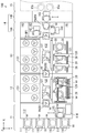
- FIG. 5 is a schematic plan view of a substrate processing apparatus provided with the development processing unit 139 of FIG.
- arrows indicating the X direction, the Y direction, and the Z direction orthogonal to each other are attached in order to clarify the positional relationship.
- the X direction and the Y direction are orthogonal to each other in the horizontal plane, and the Z direction corresponds to the vertical direction.
- the substrate processing apparatus 100 includes an indexer block 11, a coating block 12, a coating and developing block 13, a cleaning / drying processing block 14A, and a loading / unloading block 14B.
- the cleaning / drying processing block 14A and the carry-in / carry-out block 14B constitute an interface block 14.
- the exposure device 15 is disposed adjacent to the carry-in / carry-out block 14B. In the exposure apparatus 15, an exposure process is performed on the substrate W.
- the indexer block 11 includes a plurality of carrier placement units 111 and a conveyance unit 112. On each carrier placement section 111, a carrier 113 that houses a plurality of substrates W in multiple stages is placed.
- the transport unit 112 is provided with a main controller 114 and a transport mechanism 115.
- the main controller 114 controls various components of the substrate processing apparatus 100.
- the transport mechanism 115 transports the substrate W while holding the substrate W.
- the coating block 12 includes a coating processing unit 121, a transport unit 122, and a heat treatment unit 123.
- the coating processing unit 121 and the heat treatment unit 123 are opposed to each other with the conveyance unit 122 interposed therebetween.
- substrate platforms PASS1 to PASS4 (see FIG. 8) on which the substrate W is mounted are provided.
- the transport unit 122 is provided with transport mechanisms (transport robots) 127 and 128 (see FIG. 8) for transporting the substrate W.
- the coating and developing block 13 includes a coating and developing processing unit 131, a conveying unit 132, and a heat treatment unit 133.
- the coating and developing processing unit 131 and the heat treatment unit 133 are opposed to each other with the transport unit 132 interposed therebetween.
- substrate platforms PASS5 to PASS8 (see FIG. 8) on which the substrate W is mounted are provided.
- the transport unit 132 is provided with transport mechanisms 137 and 138 (see FIG. 8) for transporting the substrate W.
- the cleaning / drying processing block 14 ⁇ / b> A includes cleaning / drying processing units 161 and 162 and a transport unit 163.
- the cleaning / drying processing units 161 and 162 are opposed to each other with the conveyance unit 163 interposed therebetween.
- the transport unit 163 is provided with transport mechanisms 141 and 142.
- placement / buffer units P-BF1 and P-BF2 are provided between the transport unit 163 and the transport unit 132.
- the placement / buffer units P-BF1 and P-BF2 are configured to accommodate a plurality of substrates W.
- a substrate platform PASS9 and a later-described placement / cooling unit P-CP are provided between the transport mechanisms 141 and 142 so as to be adjacent to the carry-in / carry-out block 14B.
- the placement / cooling unit P-CP has a function of cooling the substrate W (for example, a cooling plate). In the placement / cooling section P-CP, the substrate W is cooled to a temperature suitable for the exposure process.
- a transport mechanism 143 is provided in the carry-in / carry-out block 14B.
- the transport mechanism 143 carries the substrate W into and out of the exposure apparatus 15.
- the exposure apparatus 15 is provided with a substrate carry-in portion 15a for carrying in the substrate W and a substrate carry-out portion 15b for carrying out the substrate W.
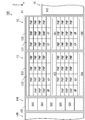
- FIG. 6 is a schematic side view showing the internal configuration of the application processing unit 121, the application development processing unit 131, and the cleaning / drying processing unit 161 in FIG.
- the coating processing section 121 is provided with coating processing chambers 21, 22, 23, and 24 in a hierarchical manner.
- the coating development processing unit 131 is provided with development processing chambers 31 and 33 and coating processing chambers 32 and 34 in a hierarchical manner.
- Each of the coating processing chambers 21 to 24, 32, and 34 is provided with a coating processing unit (spin coater) 129.
- Each development processing chamber 31, 33 is provided with the development processing unit 139 shown in FIG.
- Each coating processing unit 129 includes a spin chuck 25 that holds the substrate W and a cup 27 that is provided so as to cover the periphery of the spin chuck 25.
- each coating processing unit 129 is provided with two sets of spin chucks 25 and cups 27.
- the spin chuck 25 is rotationally driven by a driving device (not shown) (for example, an electric motor).
- each coating processing unit 129 includes a plurality of coating liquid nozzles 28 that discharge the coating liquid and a nozzle transport mechanism 29 that transports the coating liquid nozzle 28.
- the spin chuck 25 is rotated by a driving device (not shown), and any one of the plurality of coating liquid nozzles 28 is moved above the substrate W by the nozzle transport mechanism 29.
- the coating liquid is discharged from the coating liquid nozzle 28.
- the coating liquid is applied onto the substrate W.
- a rinse liquid is discharged from the edge rinse nozzle (not shown) to the peripheral edge of the substrate W.
- the coating liquid adhering to the peripheral edge portion of the substrate W is removed.
- the coating liquid for the organic coating film F1 in FIG. 2 is supplied from the coating liquid nozzle 28 to the substrate W.
- the coating liquid for the metal-containing coating film F2 in FIG. 2 is supplied from the coating liquid nozzle 28 to the substrate W.
- the coating solution for the organic coating film F3 in FIG. 2 is supplied from the coating solution nozzle 28 to the substrate W.
- a development processing unit 139 is arranged such that a plurality of spin chucks 35 are arranged in the X direction and the moving mechanism 39 is movable in the X direction.
- the cleaning / drying processing unit 161 is provided with a plurality (four in this example) of cleaning / drying processing units SD1.
- the substrate W before the exposure processing is cleaned and dried.
- FIG. 7 is a schematic side view showing the internal configuration of the heat treatment units 123 and 133 and the cleaning / drying processing unit 162 of FIG.
- the heat treatment part 123 includes an upper heat treatment part 101 provided above and a lower heat treatment part 102 provided below.
- the upper heat treatment unit 101 and the lower heat treatment unit 102 are provided with a plurality of heat treatment units PHP and a plurality of cooling units CP.
- the heat treatment unit PHP the substrate W is heated and cooled.
- the cooling unit CP the substrate W is cooled.
- the local controller LC1 is provided at the top of the heat treatment unit 123.
- the local controller LC1 controls operations of the coating processing unit 121, the transport unit 122, and the heat treatment unit 123 based on a command from the main controller 114 in FIG.
- the heat treatment part 133 includes an upper heat treatment part 103 provided above and a lower heat treatment part 104 provided below.
- the upper heat treatment unit 103 and the lower heat treatment unit 104 are provided with a cooling unit CP and a plurality of heat treatment units PHP.
- the local controller LC2 is provided at the top of the heat treatment unit 133.
- the local controller LC2 controls the operations of the coating / development processing unit 131, the transport unit 132, and the heat treatment unit 133 based on a command from the main controller 114 in FIG.
- the cleaning / drying processing section 162 is provided with a plurality (five in this example) of cleaning / drying processing units SD2.
- the substrate W after the exposure processing is cleaned and dried.
- FIG. 8 is a schematic side view showing the internal configuration of the conveying units 122, 132, and 163.
- the transfer unit 122 includes an upper transfer chamber 125 and a lower transfer chamber 126.
- the transfer unit 132 includes an upper transfer chamber 135 and a lower transfer chamber 136.
- the upper transfer chamber 125 is provided with a transfer mechanism 127
- the lower transfer chamber 126 is provided with a transfer mechanism 128.
- the upper transfer chamber 135 is provided with a transfer mechanism 137
- the lower transfer chamber 136 is provided with a transfer mechanism 138.
- substrate platforms PASS ⁇ b> 1 and PASS ⁇ b> 2 are provided between the transport unit 112 and the upper transport chamber 125, and the substrate platform is placed between the transport unit 112 and the lower transport chamber 126.
- PASS3 and PASS4 are provided.
- Substrate platforms PASS5 and PASS6 are provided between the upper transport chamber 125 and the upper transport chamber 135, and substrate platforms PASS7 and PASS8 are provided between the lower transport chamber 126 and the lower transport chamber 136. It is done.
- a placement / buffer unit P-BF1 is provided between the upper transfer chamber 135 and the transfer unit 163, and a placement / buffer unit P-BF2 is provided between the lower transfer chamber 136 and the transfer unit 163. .
- a substrate platform PASS9 and a plurality of placement / cooling units P-CP are provided so as to be adjacent to the carry-in / carry-out block 14B in the transport unit 163.
- the transport mechanism 127 delivers the substrate W to the coating processing chambers 21 and 22 (FIG. 6), the substrate platforms PASS1, PASS2, PASS5, PASS6 (FIG. 8) and the upper thermal processing unit 101 (FIG. 7).
- the transport mechanism 128 delivers the substrate W to the coating processing chambers 23 and 24 (FIG. 6), the substrate platforms PASS3, PASS4, PASS7, PASS8 (FIG. 8) and the lower thermal processing unit 102 (FIG. 7).
- the transport mechanism 137 includes a development processing chamber 31 (FIG. 6), a coating processing chamber 32 (FIG. 6), a substrate platform PASS5, PASS6 (FIG. 8), a placement / buffer unit P-BF1 (FIG. 8), and an upper stage heat treatment.
- the substrate W is delivered to the unit 103 (FIG. 7).
- the transport mechanism 138 includes a development processing chamber 33 (FIG. 6), a coating processing chamber 34 (FIG. 6), a substrate platform PASS7, PASS8 (FIG. 8), a placement / buffer unit P-BF2 (FIG. 8), and a lower heat treatment.
- the substrate W is delivered to the unit 104 (FIG. 7).
- the substrate processing will be described with reference to FIGS.
- a carrier 113 in which an unprocessed substrate W is accommodated is placed on the carrier placement portion 111 (FIG. 5) of the indexer block 11.
- the transport mechanism 115 transports the unprocessed substrate W from the carrier 113 to the substrate platforms PASS1 and PASS3 (FIG. 8).
- the transport mechanism 115 transports the processed substrate W placed on the substrate platforms PASS ⁇ b> 2 and PASS ⁇ b> 4 (FIG. 8) to the carrier 113.
- the transport mechanism 127 sequentially transports the unprocessed substrate W placed on the substrate platform PASS1 to the cooling unit CP (FIG. 7) and the coating processing chamber 22 (FIG. 6). .
- the transport mechanism 127 transfers the substrate W in the coating processing chamber 22 to the heat treatment unit PHP (FIG. 7), the cooling unit CP (FIG. 7), the coating processing chamber 21 (FIG. 6), the heat treatment unit PHP (FIG. 7), and The substrate is sequentially transferred to the substrate platform PASS5 (FIG. 8).
- the substrate W is cooled to a temperature suitable for the formation of the organic coating film F1 (FIG. 2) in the cooling unit CP.
- an organic coating film F1 is formed on the substrate W by the coating processing unit 129 (FIG. 6).
- the substrate W is cooled to a temperature suitable for forming the metal-containing coating film F2 (FIG. 2) in the cooling unit CP.
- a metal-containing coating film F2 is formed on the substrate W by the coating processing unit 129 (FIG. 6).
- the substrate W is heat-treated in the heat treatment unit PHP, and the substrate W is placed on the substrate platform PASS5.
- the transport mechanism 127 transports the substrate W after the development process, the replacement process, and the rinse process placed on the substrate platform PASS6 (FIG. 8) to the substrate platform PASS2 (FIG. 8).
- the transport mechanism 128 sequentially transports the unprocessed substrate W placed on the substrate platform PASS3 to the cooling unit CP (FIG. 7) and the coating processing chamber 24 (FIG. 6). Next, the transport mechanism 128 transfers the substrate W in the coating processing chamber 24 to the thermal processing unit PHP (FIG. 7), the cooling unit CP (FIG. 7), the coating processing chamber 23 (FIG. 6), the thermal processing unit PHP (FIG. 7), and The substrate is sequentially transferred to the substrate platform PASS7 (FIG. 8).
- the transport mechanism 128 transports the substrate W after the development process, the replacement process, and the rinsing process placed on the substrate platform PASS8 (FIG. 8) to the substrate platform PASS4 (FIG. 8).
- the processing contents of the substrate W in the coating processing chambers 23 and 24 (FIG. 6) and the lower thermal processing section 102 (FIG. 7) are the same as those in the coating processing chambers 21 and 22 (FIG. 6) and the upper thermal processing section 101 (FIG. 7).
- the processing contents of W are the same.
- the transport mechanism 137 uses the cooling unit CP (FIG. 7) and the coating processing chamber 32 (FIG. 7) to form the substrate W after the metal-containing coating film F2 formed on the substrate platform PASS5 is formed. 6), sequentially transported to the heat treatment unit PHP (FIG. 7) and the placement / buffer unit P-BF1 (FIG. 8).
- the substrate W is cooled to a temperature suitable for forming the organic coating film F3 (FIG. 2) in the cooling unit CP.
- an organic coating film F3 is formed on the substrate W by the coating processing unit 129 (FIG. 6).
- the substrate W is subjected to heat treatment in the heat treatment unit PHP, and the substrate W is placed on the placement / buffer unit P-BF1.
- the transport mechanism 137 takes out the substrate W after the exposure processing and after the heat treatment from the heat treatment unit PHP (FIG. 7) adjacent to the cleaning / drying processing block 14A.
- the transport mechanism 137 sequentially transports the substrate W to the cooling unit CP (FIG. 7), the development processing chamber 31 (FIG. 6), the heat treatment unit PHP (FIG. 7), and the substrate platform PASS6 (FIG. 8).
- the development processing unit 139 performs development processing, replacement processing, and rinsing processing of the substrate W in the development processing chamber 31. Thereafter, the substrate W is heat-treated in the heat treatment unit PHP, and the substrate W is placed on the substrate platform PASS6.
- the transport mechanism 138 transfers the substrate W after the metal-containing coating film formed on the substrate platform PASS7 to the cooling unit CP (FIG. 7), the coating processing chamber 34 (FIG. 6), and the heat treatment unit PHP ( 7) and the placement / buffer unit P-BF2 (FIG. 8) in order.
- the transport mechanism 138 takes out the substrate W after the exposure process and after the heat treatment from the heat treatment unit PHP (FIG. 7) adjacent to the interface block 14.
- the transport mechanism 138 sequentially transports the substrate W to the cooling unit CP (FIG. 7), the development processing chamber 33 (FIG. 6), the heat treatment unit PHP (FIG. 7), and the substrate platform PASS8 (FIG. 8).
- the processing content of the substrate W in the development processing chamber 33, the coating processing chamber 34, and the lower thermal processing section 104 is the same as the processing content of the substrate W in the development processing chamber 31, the coating processing chamber 32, and the upper thermal processing section 103, respectively.
- the transport mechanism 141 (FIG. 5) performs the cleaning / drying processing unit SD1 (FIG. 6) and the substrate W placed on the placement / buffer units P-BF1, P-BF2 (FIG. 8) and It is sequentially conveyed to the placement / cooling section P-CP (FIG. 8).
- the substrate W is cooled to a temperature suitable for the exposure processing by the exposure device 15 (FIG. 5) in the placement / cooling unit P-CP. Is done.
- the transport mechanism 142 (FIG. 5) cleans the substrate W after the exposure processing placed on the substrate platform PASS9 (FIG. 8) by the cleaning / drying processing unit SD2 (FIG. 7) and the upper thermal processing unit 103 or the lower thermal processing unit 104. It conveys in order to heat processing unit PHP (FIG. 7).
- a post-exposure bake (PEB) process is performed in the heat treatment unit PHP.
- the transport mechanism 143 transfers the substrate W placed on the placement / cooling unit P-CP (FIG. 8) before exposure processing to the substrate carry-in unit 15a (FIG. 5) of the exposure apparatus 15. ). Further, the transport mechanism 143 (FIG. 5) takes out the substrate W after the exposure processing from the substrate carry-out portion 15b (FIG. 5) of the exposure apparatus 15, and transports the substrate W to the substrate platform PASS9 (FIG. 8).
- the processing of the substrate W in the coating processing chambers 21, 22, 32, the development processing chamber 31 and the upper thermal processing units 101, 103 provided in the upper stage, and the coating processing chambers 23, 24 provided in the lower stage. , 34, the processing chamber 33 and the processing of the substrate W in the lower thermal processing sections 102, 104 can be performed in parallel. Thereby, the throughput can be improved without increasing the footprint.
- the organic coating film F1 is formed on one surface of the substrate W by the coating processing units 129 in the coating processing chambers 22 and 24. Further, the metal-containing coating film F2 is formed on the organic coating film F1 by the coating processing unit 129 of the coating processing chambers 21 and 23. Further, an organic coating film F3 made of a photosensitive organic material is formed on the metal-containing coating film F2 by the coating processing unit 129 in the coating processing chambers 32 and. The organic coating film F3 is exposed to a predetermined pattern by the exposure device 15.
- the developer is supplied to the organic coating film F3 by the slit nozzle 38.
- the organic coating film F3 is developed, and a predetermined pattern is formed on the organic coating film F3.
- the replacement liquid is supplied from the replacement nozzle 30 to the pattern of the organic coating film F3 and the metal-containing coating film F2.
- the portion of the metal-containing coating film F2 exposed from the pattern of the organic coating film F3 is removed, and a predetermined pattern is formed on the metal-containing coating film F2.
- the rinsing liquid is supplied from the rinse nozzle 36 to the substrate W having the pattern of the organic coating film F3 and the pattern of the metal-containing coating film F2.
- the substrate W on which the pattern of the organic coating film F3 and the pattern of the metal-containing coating film F2 are formed can be cleaned with the rinse liquid.
- the bonding force of the pattern of the metal-containing coating film F2 to the substrate W is larger than the bonding force of the pattern of the organic coating film F3 to the substrate W. Therefore, the pattern of the metal-containing coating film F2 can remain without collapsing even when a larger surface tension is applied. Therefore, even when the pattern of the organic coating film F3 collapses due to the surface tension of the rinsing liquid in the cleaning described above, the pattern of the metal-containing coating film F2 can be prevented from collapsing.
- the organic coating film F1 into a predetermined pattern using the pattern of the formed metal-containing coating film F2.
- the organic coating film F1 since the organic coating film F1 has a relatively large thickness, a pattern of the organic coating film F1 having a large thickness and a small width can be formed.
- the removal of the pattern of the organic coating film F3 and the transfer of the pattern of the metal-containing coating film F2 to the organic coating film F1 are not performed.
- the present invention is not limited to this.
- the pattern of the organic coating film F3 may be removed and the pattern of the metal-containing coating film F2 may be transferred to the organic coating film F1.
- FIG. 9 is a schematic plan view showing a configuration of a development processing unit according to another embodiment.
- a development processing unit 139X according to another embodiment will be described while referring to differences from the development processing unit 139 of FIG.
- the development processing unit 139 ⁇ / b> X according to the present embodiment further includes a plurality of replacement nozzles 40. In the present embodiment, three replacement nozzles 40 are provided in the development processing unit 139X.
- the replacement nozzle 40 is provided to be rotatable between a retracted position outside the cup 37 and a processing position above the central portion of the substrate W held by the spin chuck 35. During the replacement process, the replacement nozzle 40 is moved to the processing position. The replacement process of the substrate W is performed by discharging the replacement liquid from the replacement nozzle 40 while the spin chuck 35 rotates. As the replacement liquid discharged from the replacement nozzle 40, for example, an aqueous solution containing sulfuric acid and hydrogen peroxide is used.
- FIG. 10 is a diagram for explaining the operation of the development processing unit 139X of FIG.
- the replacement process of FIGS. 10A to 10C is performed between the replacement process of FIG. 4A and the rinse process of FIG. 4B.
- the replacement liquid 5 is supplied from the replacement nozzle 40 (FIG. 9) to the substrate W as shown in FIG. 10A.
- a liquid layer of the replacement liquid 5 is formed on the surface to be processed of the substrate W, and the replacement liquid 3 remaining on the surface to be processed of the substrate W is replaced with the replacement liquid 5.
- the organic coating film F ⁇ b> 3 is removed by holding the liquid layer of the replacement liquid 5.
- the pattern of the organic coating film F3 is removed and the pattern of the metal-containing coating film F2 is transferred to the organic coating film F1, but the present invention is not limited to this.
- the pattern of the organic coating film F3 is removed, and the pattern of the metal-containing coating film F2 may not be transferred to the organic coating film F1.
- the rinse process of FIG. 4B is performed without performing the replacement process of FIG. 10C.
- the development processing unit 139X is provided with a replacement nozzle 40 for removing the pattern of the organic coating film F3 and transferring the pattern of the metal-containing coating film F2 to the organic coating film F1.
- the replacement nozzle 40 may be provided in another unit of the substrate processing apparatus 100 without being provided in the development processing unit 139X.
- the development processing units 139 and 139X have the slit nozzle 38 for supplying the developer to the substrate W, but the present invention is not limited to this.
- an alkaline aqueous solution such as TMAH or KOH (potassium hydroxide) is used as the replacement liquid supplied from the replacement nozzle 30, the positive tone development process can be performed on the substrate W with the replacement liquid.
- the development processing units 139 and 139X may not have the slit nozzle 38. Further, in this configuration, the development processing in FIGS. 3A and 3B is omitted. This configuration corresponds to the invention according to the above-mentioned other aspect and the invention according to still another aspect.
- the organic coating film F1 is formed between the substrate W and the metal-containing coating film F2, but the present invention is not limited to this.
- the organic coating film F1 may not be formed.
- the substrate W is an example of a substrate
- the development processing units 139 and 139X are examples of a developing device
- the metal-containing coating film F2 is an example of a metal-containing coating film
- the organic coating film F3 F1 is an example of the first and second organic coating films, respectively.
- the slit nozzle 38 is an example of a developer supply unit
- the replacement nozzle 30 is an example of a first removal solution supply unit
- the rinse nozzle 36 is an example of a rinse solution supply unit
- the spin chuck 35 is a rotation holding unit. It is an example.
- the replacement nozzle 40 is an example of second and third removal liquid supply units
- the exposure apparatus 15 is an example of an exposure apparatus
- the substrate processing apparatus 100 is an example of a substrate processing apparatus
- the coating processing chambers 21 and 23 The coating processing unit 129 is an example of a metal-containing coating film forming unit.
- the coating processing unit 129 in the coating processing chambers 32 and 34 is an example of the first organic coating film forming unit
- the coating processing unit 129 in the coating processing chambers 22 and 24 is an example of the second organic coating film forming unit.
- the present invention can be effectively used for substrate processing using various processing solutions.
Landscapes
- Physics & Mathematics (AREA)
- General Physics & Mathematics (AREA)
- Photosensitive Polymer And Photoresist Processing (AREA)
- Cleaning Or Drying Semiconductors (AREA)
- Exposure Of Semiconductors, Excluding Electron Or Ion Beam Exposure (AREA)
Abstract
基板の一面上には、金属含有塗布膜が形成され、金属含有塗布膜上に感光性の有機材料により有機塗布膜が形成され、有機塗布膜は所定のパターンに露光されている。有機塗布膜に現像液がスリットノズルにより供給されることにより、有機塗布膜に所定のパターンが形成される。また、置換液が置換ノズルにより有機塗布膜のパターンおよび金属含有塗布膜に供給されることにより、金属含有塗布膜の部分が除去され、金属含有塗布膜に所定のパターンが形成される。リンス液がリンスノズルにより有機塗布膜のパターンおよび金属含有塗布膜のパターンを有する基板に供給される。
Description
本発明は、基板の現像を行う現像装置、基板処理装置、現像方法および基板処理方法に関する。
半導体デバイス等の製造におけるリソグラフィ工程では、基板上にレジスト液等の塗布液が供給されることにより塗布膜が形成される。塗布膜が露光された後、現像されることにより、塗布膜に所定のパターンが形成される。塗布膜にパターが形成された後の基板には、リンス処理が行われる。ここで、塗布膜のパターンの厚みが大きくかつ幅が小さい場合には、リンス処理におけるリンス液の表面張力によりパターンの倒壊が発生することがある(例えば、特許文献1,2参照)。
特許文献1には、リンス液にイソプロビル・アルコールを混入し、リンス液の表面張力を低下させることによりパターンの倒壊を防止することが記載されている。引用文献2には、リンス処理後、比重1.5以上でかつ表面張力dyns/cm以下のフッ素系不活性液体をリンス液と置換することによりパターンの倒壊を防止することが記載されている。
特開平7-122485号公報
特開平9-82629号公報
近年、基板に形成されるチップの高集積化が進んでいる。この場合、塗布膜のパターン幅の微細化に伴い、パターンの倒壊が発生し、歩留まりが低下しやすくなる。そのため、パターンの倒壊をより確実に防止することが求められる。
本発明の目的は、塗布膜のパターンの倒壊を防止することが可能な現像装置、基板処理装置、現像方法および基板処理方法を提供することである。
(1)本発明の一局面に従う現像装置は、基板に現像処理を行う現像装置であって、基板の一面上には、金属を含有する塗布液の膜が金属含有塗布膜として形成され、金属含有塗布膜上に感光性の有機材料により形成されかつ所定のパターンに露光された第1の有機塗布膜が形成され、現像装置は、現像液を第1の有機塗布膜に供給することにより所定のパターンを有する第1の有機塗布膜パターンを形成する現像液供給部と、金属を除去するための第1の除去液を第1の有機塗布膜パターンおよび金属含有塗布膜に供給することにより所定のパターンを有する金属含有塗布膜パターンを形成する第1の除去液供給部と、第1の有機塗布膜パターンおよび金属含有塗布膜パターンを有する基板にリンス液を供給するリンス液供給部とを備える。
基板の一面上には、金属含有塗布膜が形成され、金属含有塗布膜上に感光性の有機材料により第1の有機塗布膜が形成され、第1の有機塗布膜は所定のパターンに露光されている。この現像装置においては、第1の有機塗布膜に現像液が現像液供給部により供給される。これにより、第1の有機塗布膜が現像され、所定のパターンを有する第1の有機塗布膜パターンが形成される。また、第1の除去液が第1の除去液供給部により第1の有機塗布膜パターンおよび金属含有塗布膜に供給される。これにより、第1の有機塗布膜パターンから露出する金属含有塗布膜の部分が除去され、所定のパターンを有する金属含有塗布膜パターンが形成される。その後、リンス液がリンス液供給部により第1の有機塗布膜パターンおよび金属含有塗布膜パターンを有する基板に供給される。
この構成によれば、第1の有機塗布膜パターンおよび金属含有塗布膜パターンが形成された基板をリンス液により洗浄することができる。ここで、基板に対する金属含有塗布膜パターンの接合力は、基板に対する第1の有機塗布膜パターンの接合力よりも大きい。そのため、金属含有塗布膜パターンは、より大きい表面張力が加えられた場合でも、倒壊することなく残存することが可能である。したがって、上記の洗浄においてリンス液の表面張力により第1の有機塗布膜パターンが倒壊する場合でも、金属含有塗布膜パターンが倒壊することを防止することができる。
(2)第1の除去液は、キレート剤が添加された水溶液、アルカリ性水溶液または酸性水溶液を含んでもよい。この場合、金属含有塗布膜の部分を容易に除去することができる。
(3)キレート剤は、有機酸、有機酸の塩、アミノ酸、アミノ酸の誘導体、無機アルカリ、無機アルカリの塩、アルキルアミン、アルキルアミンの誘導体、アルカノールアミンおよびアルカノールアミンの誘導体よりなる群から選択された一種または複数種を含んでもよい。この場合、金属含有塗布膜の部分をより容易に除去することができる。
(4)本発明の他の局面に従う現像装置は、基板に現像処理を行う現像装置であって、基板の一面上には、金属を含有する塗布液の膜が金属含有塗布膜として形成され、金属含有塗布膜上に感光性の有機材料により形成されかつ所定のパターンに露光された第1の有機塗布膜が形成され、現像装置は、金属を除去するための第1の除去液を第1の有機塗布膜および金属含有塗布膜に供給することにより所定のパターンを有する第1の有機塗布膜パターンおよび所定のパターンを有する金属含有塗布膜パターンを形成する第1の除去液供給部と、第1の有機塗布膜パターンおよび金属含有塗布膜パターンを有する基板にリンス液を供給するリンス液供給部とを備える。
基板の一面上には、金属含有塗布膜が形成され、金属含有塗布膜上に感光性の有機材料により第1の有機塗布膜が形成され、第1の有機塗布膜は所定のパターンに露光されている。この現像装置においては、第1の有機塗布膜および金属含有塗布膜に第1の除去液が第1の除去液供給部により供給される。これにより、第1の有機塗布膜が現像され、所定のパターンを有する第1の有機塗布膜パターンが形成される。また、第1の有機塗布膜パターンから露出する金属含有塗布膜の部分が除去され、所定のパターンを有する金属含有塗布膜パターンが形成される。その後、リンス液がリンス液供給部により第1の有機塗布膜パターンおよび金属含有塗布膜パターンを有する基板に供給される。
この構成によれば、第1の有機塗布膜パターンおよび金属含有塗布膜パターンが形成された基板をリンス液により洗浄することができる。ここで、基板に対する金属含有塗布膜パターンの接合力は、基板に対する第1の有機塗布膜パターンの接合力よりも大きい。そのため、金属含有塗布膜パターンは、より大きい表面張力が加えられた場合でも、倒壊することなく残存することが可能である。したがって、上記の洗浄においてリンス液の表面張力により第1の有機塗布膜パターンが倒壊する場合でも、金属含有塗布膜パターンが倒壊することを防止することができる。
(5)第1の除去液は、アルカリ性水溶液を含んでもよい。この場合、第1の有機塗布膜を現像しつつ金属含有塗布膜の部分を容易に除去することができる。
(6)現像装置は、基板を保持するとともに、リンス液供給部によりリンス液が供給された後の基板を回転させる回転保持部をさらに備えてもよい。この場合、リンス液が供給された基板を短時間で乾燥させることができる。また、金属含有塗布膜パターンと基板との接合力は大きいので、基板の回転により金属含有塗布膜パターンに遠心力が加えられた場合でも、金属含有塗布膜パターンが倒壊することを防止することができる。
(7)現像装置は、第1の除去液供給部により第1の除去液が供給された後でかつリンス液供給部によりリンス液が供給される前の基板に第1の有機塗布膜パターンを除去するための第2の除去液を供給する第2の除去液供給部をさらに備えてもよい。この場合、金属含有塗布膜パターンが形成された後に不要となった第1の有機塗布膜パターンを簡単な構成で除去することができる。
(8)基板には、一面と金属含有塗布膜との間に第2の有機塗布膜がさらに形成されていてもよい。この場合、形成された金属含有塗布膜パターンを用いて第2の有機塗布膜を所定のパターンに形成することが可能となる。また、第2の有機塗布膜を厚く形成することにより、厚みが大きくかつ幅が小さい第2の有機塗布膜のパターンを形成することが可能となる。
(9)現像装置は、第1の除去液供給部により第1の除去液が供給された後でかつリンス液供給部によりリンス液が供給される前の基板に第2の有機塗布膜を除去するための第3の除去液を供給することにより所定のパターンを有する第2の有機塗布膜パターンを形成する第3の除去液供給部をさらに備えてもよい。
この場合、金属含有塗布膜パターンから露出する第2の有機塗布膜の部分が第3の除去液により除去される。これにより、所定のパターンを有する第2の有機塗布膜パターンを容易に形成することができる。
(10)本発明のさらに他の局面に従う基板処理装置は、基板を露光する露光装置に隣接するように配置される基板処理装置であって、金属を含有する塗布液を金属含有塗布液として基板の一面に供給することにより一面上に金属含有塗布膜を形成する金属含有塗布膜形成部と、感光性材料により形成される第1の有機塗布液を金属含有塗布膜に供給することにより金属含有塗布膜形成部により形成された金属含有塗布膜上に第1の有機塗布膜を形成する第1の有機塗布膜形成部と、第1の有機塗布膜形成部により形成された第1の有機塗布膜が露光装置により所定のパターンに露光された基板に現像処理を行う本発明の一局面または他の局面に従う現像装置とを備える。
この基板処理装置においては、金属含有塗布膜形成部により金属含有塗布液が基板の一面に供給される。これにより、基板の一面上に金属含有塗布膜が形成される。感光性材料により形成される第1の有機塗布液が第1の有機塗布膜形成部により金属含有塗布膜に供給される。これにより、金属含有塗布膜形成部により形成された金属含有塗布膜上に第1の有機塗布膜が形成される。露光装置においては、第1の有機塗布膜形成部により形成された第1の有機塗布膜が所定のパターンに露光される。
現像装置においては、所定のパターンに露光された第1の有機塗布膜に現像液が現像液供給部により供給される。これにより、第1の有機塗布膜が現像され、所定のパターンを有する第1の有機塗布膜パターンが形成される。第1の除去液が第1の除去液供給部により第1の有機塗布膜パターンおよび金属含有塗布膜に供給される。これにより、第1の有機塗布膜パターンから露出する金属含有塗布膜の部分が除去され、所定のパターンを有する金属含有塗布膜パターンが形成される。その後、リンス液がリンス液供給部により第1の有機塗布膜パターンおよび金属含有塗布膜パターンを有する基板に供給される。
この構成によれば、第1の有機塗布膜パターンおよび金属含有塗布膜パターンが形成された基板をリンス液により洗浄することができる。ここで、基板に対する金属含有塗布膜パターンの接合力は、基板に対する第1の有機塗布膜パターンの接合力よりも大きい。そのため、金属含有塗布膜パターンは、より大きい表面張力が加えられた場合でも、倒壊することなく残存することが可能である。したがって、上記の洗浄においてリンス液の表面張力により第1の有機塗布膜パターンが倒壊する場合でも、金属含有塗布膜パターンが倒壊することを防止することができる。
(11)基板処理装置は、金属含有塗布膜形成部により基板の一面に金属含有塗布膜が形成される前に、第2の有機塗布液を基板の一面に供給することにより一面と金属含有塗布膜との間に第2の有機塗布膜を形成する第2の有機塗布膜形成部をさらに備えてもよい。
この場合、基板の一面と金属含有塗布膜との間に第2の有機塗布膜が形成される。これにより、金属含有塗布膜パターンを用いて第2の有機塗布膜を所定のパターンに形成することが可能となる。また、第2の有機塗布膜を厚く形成することにより、厚みが大きくかつ幅が小さい第2の有機塗布膜のパターンを形成することが可能となる。
(12)本発明のさらに他の局面に従う現像方法は、基板に現像処理を行う現像方法であって、基板の一面上には、金属を含有する塗布液の膜が金属含有塗布膜として形成され、金属含有塗布膜上に感光性の有機材料により形成されかつ所定のパターンに露光された第1の有機塗布膜が形成され、現像方法は、現像液を現像液供給部により第1の有機塗布膜に供給することにより所定のパターンを有する第1の有機塗布膜パターンを形成するステップと、金属を除去するための第1の除去液を第1の除去液供給部により第1の有機塗布膜パターンおよび金属含有塗布膜に供給することにより所定のパターンを有する金属含有塗布膜パターンを形成するステップと、リンス液をリンス液供給部により第1の有機塗布膜パターンおよび金属含有塗布膜パターンを有する基板に供給するステップとを含む。
基板の一面上には、金属含有塗布膜が形成され、金属含有塗布膜上に感光性の有機材料により第1の有機塗布膜が形成され、第1の有機塗布膜は所定のパターンに露光されている。この現像方法によれば、第1の有機塗布膜に現像液が現像液供給部により供給される。これにより、第1の有機塗布膜が現像され、所定のパターンを有する第1の有機塗布膜パターンが形成される。また、第1の除去液が第1の除去液供給部により第1の有機塗布膜パターンおよび金属含有塗布膜に供給される。これにより、第1の有機塗布膜パターンから露出する金属含有塗布膜の部分が除去され、所定のパターンを有する金属含有塗布膜パターンが形成される。その後、リンス液がリンス液供給部により第1の有機塗布膜パターンおよび金属含有塗布膜パターンを有する基板に供給される。
この方法によれば、第1の有機塗布膜パターンおよび金属含有塗布膜パターンが形成された基板をリンス液により洗浄することができる。ここで、基板に対する金属含有塗布膜パターンの接合力は、基板に対する第1の有機塗布膜パターンの接合力よりも大きい。そのため、金属含有塗布膜パターンは、より大きい表面張力が加えられた場合でも、倒壊することなく残存することが可能である。したがって、上記の洗浄においてリンス液の表面張力により第1の有機塗布膜パターンが倒壊する場合でも、金属含有塗布膜パターンが倒壊することを防止することができる。
(13)本発明のさらに他の局面に従う現像方法は、基板に現像処理を行う現像方法であって、基板の一面上には、金属を含有する塗布液の膜が金属含有塗布膜として形成され、金属含有塗布膜上に感光性の有機材料により形成されかつ所定のパターンに露光された第1の有機塗布膜が形成され、現像方法は、金属を除去するための第1の除去液を第1の除去液供給部により第1の有機塗布膜および金属含有塗布膜に供給することにより所定のパターンを有する第1の有機塗布膜パターンおよび所定のパターンを有する金属含有塗布膜パターンを形成するステップと、リンス液をリンス液供給部により第1の有機塗布膜パターンおよび金属含有塗布膜パターンを有する基板に供給するステップとを含む。
基板の一面上には、金属含有塗布膜が形成され、金属含有塗布膜上に感光性の有機材料により第1の有機塗布膜が形成され、第1の有機塗布膜は所定のパターンに露光されている。この現像方法によれば、第1の有機塗布膜および金属含有塗布膜に第1の除去液が第1の除去液供給部により供給される。これにより、第1の有機塗布膜が現像され、所定のパターンを有する第1の有機塗布膜パターンが形成される。また、第1の有機塗布膜パターンから露出する金属含有塗布膜の部分が除去され、所定のパターンを有する金属含有塗布膜パターンが形成される。その後、リンス液がリンス液供給部により第1の有機塗布膜パターンおよび金属含有塗布膜パターンを有する基板に供給される。
この方法によれば、第1の有機塗布膜パターンおよび金属含有塗布膜パターンが形成された基板をリンス液により洗浄することができる。ここで、基板に対する金属含有塗布膜パターンの接合力は、基板に対する第1の有機塗布膜パターンの接合力よりも大きい。そのため、金属含有塗布膜パターンは、より大きい表面張力が加えられた場合でも、倒壊することなく残存することが可能である。したがって、上記の洗浄においてリンス液の表面張力により第1の有機塗布膜パターンが倒壊する場合でも、金属含有塗布膜パターンが倒壊することを防止することができる。
(14)現像方法は、リンス液供給部によりリンス液が供給された後の基板を回転保持部により保持して回転させるステップをさらに含んでもよい。この場合、リンス液が供給された基板を短時間で乾燥させることができる。また、金属含有塗布膜パターンと基板との接合力は大きいので、基板の回転により金属含有塗布膜パターンに遠心力が加えられた場合でも、金属含有塗布膜パターンが倒壊することを防止することができる。
(15)本発明のさらに他の局面に従う基板処理方法は、基板を露光する露光装置を用いた基板処理方法であって、金属を含有する塗布液を金属含有塗布液として金属含有塗布膜形成部により基板の一面に供給することにより一面上に金属含有塗布膜を形成するステップと、感光性材料により形成される第1の有機塗布液を第1の有機塗布膜形成部により金属含有塗布膜形成部により形成された金属含有塗布膜に供給することにより金属含有塗布膜形成部により形成された金属含有塗布膜上に第1の有機塗布膜を形成するステップと、第1の有機塗布膜形成部により形成された第1の有機塗布膜が露光装置により所定のパターンに露光された基板に本発明のさらに他の局面に従う現像方法を用いて現像処理を行うステップとを含む。
この基板処理方法によれば、金属含有塗布膜形成部により金属含有塗布液が基板の一面に供給される。これにより、基板の一面上に金属含有塗布膜が形成される。感光性材料により形成される第1の有機塗布液が第1の有機塗布膜形成部により金属含有塗布膜に供給される。これにより、金属含有塗布膜形成部により形成された金属含有塗布膜上に第1の有機塗布膜が形成される。露光装置においては、第1の有機塗布膜形成部により形成された第1の有機塗布膜が所定のパターンに露光される。
現像方法によれば、所定のパターンに露光された第1の有機塗布膜に現像液が現像液供給部により供給される。これにより、第1の有機塗布膜が現像され、所定のパターンを有する第1の有機塗布膜パターンが形成される。第1の除去液が第1の除去液供給部により第1の有機塗布膜パターンおよび金属含有塗布膜に供給される。これにより、第1の有機塗布膜パターンから露出する金属含有塗布膜の部分が除去され、所定のパターンを有する金属含有塗布膜パターンが形成される。その後、リンス液がリンス液供給部により第1の有機塗布膜パターンおよび金属含有塗布膜パターンを有する基板に供給される。
この方法によれば、第1の有機塗布膜パターンおよび金属含有塗布膜パターンが形成された基板をリンス液により洗浄することができる。ここで、基板に対する金属含有塗布膜パターンの接合力は、基板に対する第1の有機塗布膜パターンの接合力よりも大きい。そのため、金属含有塗布膜パターンは、より大きい表面張力が加えられた場合でも、倒壊することなく残存することが可能である。したがって、上記の洗浄においてリンス液の表面張力により第1の有機塗布膜パターンが倒壊する場合でも、金属含有塗布膜パターンが倒壊することを防止することができる。
(16)基板処理方法は、金属含有塗布膜を形成するステップの前に、第2の有機塗布液を第2の有機塗布膜形成部により基板の一面に供給することにより一面と金属含有塗布膜との間に第2の有機塗布膜を形成するステップをさらに含んでもよい。
この場合、基板の一面と金属含有塗布膜との間に第2の有機塗布膜が形成される。これにより、金属含有塗布膜パターンを用いて第2の有機塗布膜を所定のパターンに形成することが可能となる。また、第2の有機塗布膜を厚く形成することにより、厚みが大きくかつ幅が小さい第2の有機塗布膜のパターンを形成することが可能となる。
本発明によれば、塗布膜のパターンの倒壊を防止することができる。
以下、本発明の一実施の形態に係る現像装置、基板処理装置、現像方法および基板処理方法について図面を用いて説明する。なお、以下の説明において、基板とは、半導体基板、液晶表示装置もしくは有機EL(Electro Luminescence)表示装置等のFPD(Flat Panel Display)用基板、光ディスク用基板、磁気ディスク用基板、光磁気ディスク用基板、フォトマスク用基板または太陽電池用基板等をいう。
(1)現像処理ユニットの構成
図1は、本発明の一実施の形態に係る現像処理ユニットの構成を示す模式的平面図である。図1に示すように、現像処理ユニット(スピンデベロッパ)139は、複数の置換ノズル30、複数のスピンチャック35、複数のリンスノズル36および複数のカップ37を備える。また、現像処理ユニット139は、現像液を吐出する2つのスリットノズル38およびそれらのスリットノズル38を一方向に移動させる移動機構39を備える。本実施の形態においては、置換ノズル30、スピンチャック35、リンスノズル36およびカップ37は、現像処理ユニット139に3つずつ設けられる。
図1は、本発明の一実施の形態に係る現像処理ユニットの構成を示す模式的平面図である。図1に示すように、現像処理ユニット(スピンデベロッパ)139は、複数の置換ノズル30、複数のスピンチャック35、複数のリンスノズル36および複数のカップ37を備える。また、現像処理ユニット139は、現像液を吐出する2つのスリットノズル38およびそれらのスリットノズル38を一方向に移動させる移動機構39を備える。本実施の形態においては、置換ノズル30、スピンチャック35、リンスノズル36およびカップ37は、現像処理ユニット139に3つずつ設けられる。
各スピンチャック35は、基板Wを保持した状態で、図示しない駆動装置(例えば、電動モータ)により回転駆動される。カップ37はスピンチャック35の周囲を取り囲むように設けられる。各スリットノズル38には、図示しない現像液貯留部から現像液配管を通して現像液が供給される。いずれかのスリットノズル38が移動機構39により基板Wの上方に移動される。スピンチャック35が回転しつつスリットノズル38から現像液が吐出されることにより、基板Wの現像処理が行われる。
置換ノズル30は、カップ37の外側の待避位置とスピンチャック35により保持される基板Wの中心部の上方の処理位置との間で回動可能に設けられる。基板Wの現像処理後の置換処理時には、置換ノズル30が処理位置に移動される。スピンチャック35が回転しつつ置換ノズル30から置換液が吐出されることにより、基板Wの置換処理が行われる。
置換液として、例えばアルカリ性置換液または酸性置換液が用いられる。アルカリ性置換液は、例えばアンモニアおよび過酸化水素を含む水溶液である。アルカリ性置換液は、例えばTMAH(tetra methyl ammonium hydroxide:水酸化テトラメチルアンモニウム)であってもよい。酸性置換液は、例えば希フッ酸を含む水溶液である。酸性置換液は、例えば硫酸および過酸化水素を含む水溶液であってもよいし、酢酸を含む水溶液であってもよい。
あるいは、置換液は、キレート剤を含む水溶液であってもよい。キレート剤は、有機酸、有機酸の塩、アミノ酸、アミノ酸の誘導体、無機アルカリ、無機アルカリの塩、アルキルアミン、アルキルアミンの誘導体、アルカノールアミンおよびアルカノールアミンの誘導体よりなる群から選択された一種または複数種を含む。
リンスノズル36は、カップ37の外側の待避位置とスピンチャック35により保持される基板Wの中心部の上方の処理位置との間で回動可能に設けられる。基板Wの置換処理後のリンス処理時には、リンスノズル36が処理位置に移動される。スピンチャック35が回転しつつリンスノズル36からリンス液が吐出されることにより、基板Wのリンス処理が行われる。
(2)現像処理ユニットの動作
図2は、図1の現像処理ユニット139の処理対象となる基板Wの部分拡大縦断面図である。図2に示すように、基板Wの被処理面には、レジスト膜として3種類の塗布膜F1,F2,F3が形成される。具体的には、基板Wの被処理面上に塗布膜F1が形成され、塗布膜F1上に塗布膜F2が形成され、塗布膜F2上に塗布膜F3が形成される。塗布膜F1~F3は、後述する図5~図8の基板処理装置100により基板Wの被処理面上に形成される。
図2は、図1の現像処理ユニット139の処理対象となる基板Wの部分拡大縦断面図である。図2に示すように、基板Wの被処理面には、レジスト膜として3種類の塗布膜F1,F2,F3が形成される。具体的には、基板Wの被処理面上に塗布膜F1が形成され、塗布膜F1上に塗布膜F2が形成され、塗布膜F2上に塗布膜F3が形成される。塗布膜F1~F3は、後述する図5~図8の基板処理装置100により基板Wの被処理面上に形成される。
塗布膜F1は、非感光性の有機膜であり、本例ではSOC(Spin-On-Carbon)膜である。以下、塗布膜F1を有機塗布膜F1と呼ぶ。有機塗布膜F1は、比較的大きい厚みを有する。本例では、有機塗布膜F1の厚みは、例えば100nm以上でかつ300nm以下である。
塗布膜F2は、非感光性の無機膜である。塗布膜F2には、金属成分または金属酸化物等の金属成分が組成物として含有されている。本例では、金属成分として、例えばSn(スズ)、HfO2(酸化ハフニウム)またはZrO2(二酸化ジルコニウム)が塗布膜F2に含有される。以下、塗布膜F2を金属含有塗布膜F2と呼ぶ。金属含有塗布膜F2は、比較的小さい厚みを有する。本例では、金属含有塗布膜F2の厚みは、例えば5nm以上でかつ30nm以下である。
塗布膜F3は、例えば紫外領域において感光性を有する有機膜である。以下、塗布膜F3を有機塗布膜F3と呼ぶ。有機塗布膜F3は、所定のパターンに露光されている。本例では、有機塗布膜F3の厚みは、例えば20nm以上でかつ60nm以下である。なお、本実施の形態において、有機塗布膜F1および金属含有塗布膜F2は非感光性を有するが、本発明はこれに限定されない。有機塗布膜F3とは感光波長領域が異なる場合には、有機塗布膜F1および金属含有塗布膜F2は感光性を有してもよい。
図3および図4は、図1の現像処理ユニット139の動作を説明するための図である。現像処理において、図3(a)に示すように、スリットノズル38(図1)から基板Wに現像液1が供給される。これにより、基板Wの被処理面上に現像液1の液層が形成される。次に、図3(b)に示すように、リンスノズル36(図1)から基板Wにリンス液2が供給される。これにより、有機塗布膜F3の不要な部分および現像液1が除去され、有機塗布膜F3にパターンが形成される。
その後の置換処理において、図3(c)に示すように、置換ノズル30(図1)から基板Wに置換液3が供給される。これにより、基板Wの被処理面上に置換液3の液層が形成され、基板Wの被処理面に残存したリンス液2が置換液3に置換される。その後、図4(a)に示すように、置換液3の液層が保持されることにより、有機塗布膜F3から露出する金属含有塗布膜F2の部分が除去され、金属含有塗布膜F2にパターンが形成される。
その後のリンス処理において、図4(b)に示すように、リンスノズル36(図1)から基板Wにリンス液4が供給されることにより、置換液3が除去される。次に、図4(c)に示すように、基板Wがスピンチャック35(図1)により高速(例えば1000rpm以下)で回転される。これにより、基板Wに残存するリンス液4が振り切られ、基板Wが短時間で乾燥される。ここで、金属含有塗布膜F2のパターンと基板W(有機塗布膜F1)との接合力は大きいので、基板Wの回転により金属含有塗布膜F2のパターンに遠心力が加えられた場合でも、金属含有塗布膜F2のパターンは倒壊することが防止される。
なお、図3(a)~図4(b)の処理においては、基板Wはスピンチャック35により低速(例えば10rpm程度)で回転されてもよいし、停止していてもよい。基板Wが回転される場合には、現像液1または置換液3の液層が撹拌されることにより、液層の濃度を全体的に均一にすることができる。
上記の処理によれば、図4(c)に示すように、有機塗布膜F3のパターンの一部に倒壊が発生する可能性があるが、金属含有塗布膜F2のパターンには倒壊は発生しない。そのため、有機塗布膜F3のパターンを除去した後、ドライエッチング等を用いて金属含有塗布膜F2のパターンを有機塗布膜F1に転写することにより、厚みが大きくかつ幅が小さい有機塗布膜F1のパターンを倒壊させることなく形成することができる。
(3)基板処理装置の構成
図5は、図1の現像処理ユニット139を備えた基板処理装置の模式的平面図である。図5および以降の所定の図には、位置関係を明確にするために互いに直交するX方向、Y方向およびZ方向を示す矢印を付している。X方向およびY方向は水平面内で互いに直交し、Z方向は鉛直方向に相当する。
図5は、図1の現像処理ユニット139を備えた基板処理装置の模式的平面図である。図5および以降の所定の図には、位置関係を明確にするために互いに直交するX方向、Y方向およびZ方向を示す矢印を付している。X方向およびY方向は水平面内で互いに直交し、Z方向は鉛直方向に相当する。
図5に示すように、基板処理装置100は、インデクサブロック11、塗布ブロック12、塗布現像ブロック13、洗浄乾燥処理ブロック14Aおよび搬入搬出ブロック14Bを備える。洗浄乾燥処理ブロック14Aおよび搬入搬出ブロック14Bにより、インターフェイスブロック14が構成される。搬入搬出ブロック14Bに隣接するように露光装置15が配置される。露光装置15においては、基板Wに露光処理が行われる。
インデクサブロック11は、複数のキャリア載置部111および搬送部112を含む。各キャリア載置部111には、複数の基板Wを多段に収納するキャリア113が載置される。搬送部112には、メインコントローラ114および搬送機構115が設けられる。メインコントローラ114は、基板処理装置100の種々の構成要素を制御する。搬送機構115は、基板Wを保持しつつその基板Wを搬送する。
塗布ブロック12は、塗布処理部121、搬送部122および熱処理部123を含む。塗布処理部121および熱処理部123は、搬送部122を挟んで対向する。搬送部122とインデクサブロック11との間には、基板Wが載置される基板載置部PASS1~PASS4(図8参照)が設けられる。搬送部122には、基板Wを搬送する搬送機構(搬送ロボット)127,128(図8参照)が設けられる。
塗布現像ブロック13は、塗布現像処理部131、搬送部132および熱処理部133を含む。塗布現像処理部131および熱処理部133は、搬送部132を挟んで対向する。搬送部132と搬送部122との間には、基板Wが載置される基板載置部PASS5~PASS8(図8参照)が設けられる。搬送部132には、基板Wを搬送する搬送機構137,138(図8参照)が設けられる。
洗浄乾燥処理ブロック14Aは、洗浄乾燥処理部161,162および搬送部163を含む。洗浄乾燥処理部161,162は、搬送部163を挟んで対向する。搬送部163には、搬送機構141,142が設けられる。
搬送部163と搬送部132との間には、載置兼バッファ部P-BF1,P-BF2(図8参照)が設けられる。載置兼バッファ部P-BF1,P-BF2は、複数の基板Wを収容可能に構成される。
また、搬送機構141,142の間において、搬入搬出ブロック14Bに隣接するように、基板載置部PASS9および後述の載置兼冷却部P-CP(図8参照)が設けられる。載置兼冷却部P-CPは、基板Wを冷却する機能(例えば、クーリングプレート)を備える。載置兼冷却部P-CPにおいて、基板Wが露光処理に適した温度に冷却される。
搬入搬出ブロック14Bには、搬送機構143が設けられる。搬送機構143は、露光装置15に対する基板Wの搬入および搬出を行う。露光装置15には、基板Wを搬入するための基板搬入部15aおよび基板Wを搬出するための基板搬出部15bが設けられる。
(4)塗布処理部および塗布現像処理部
図6は、図5の塗布処理部121、塗布現像処理部131および洗浄乾燥処理部161の内部構成を示す模式的側面図である。図6に示すように、塗布処理部121には、塗布処理室21,22,23,24が階層的に設けられる。塗布現像処理部131には、現像処理室31,33および塗布処理室32,34が階層的に設けられる。各塗布処理室21~24,32,34には、塗布処理ユニット(スピンコータ)129が設けられる。各現像処理室31,33には、図1の現像処理ユニット139が設けられる。
図6は、図5の塗布処理部121、塗布現像処理部131および洗浄乾燥処理部161の内部構成を示す模式的側面図である。図6に示すように、塗布処理部121には、塗布処理室21,22,23,24が階層的に設けられる。塗布現像処理部131には、現像処理室31,33および塗布処理室32,34が階層的に設けられる。各塗布処理室21~24,32,34には、塗布処理ユニット(スピンコータ)129が設けられる。各現像処理室31,33には、図1の現像処理ユニット139が設けられる。
各塗布処理ユニット129は、基板Wを保持するスピンチャック25およびスピンチャック25の周囲を覆うように設けられるカップ27を備える。本実施の形態では、各塗布処理ユニット129に2組のスピンチャック25およびカップ27が設けられる。スピンチャック25は、図示しない駆動装置(例えば、電動モータ)により回転駆動される。また、図5に示すように、各塗布処理ユニット129は、塗布液を吐出する複数の塗布液ノズル28およびその塗布液ノズル28を搬送するノズル搬送機構29を備える。
塗布処理ユニット129においては、図示しない駆動装置によりスピンチャック25が回転されるとともに、複数の塗布液ノズル28のうちのいずれかの塗布液ノズル28がノズル搬送機構29により基板Wの上方に移動され、その塗布液ノズル28から塗布液が吐出される。それにより、基板W上に塗布液が塗布される。また、図示しないエッジリンスノズルから、基板Wの周縁部にリンス液が吐出される。それにより、基板Wの周縁部に付着する塗布液が除去される。
塗布処理室22,24の塗布処理ユニット129においては、図2の有機塗布膜F1用の塗布液が塗布液ノズル28から基板Wに供給される。塗布処理室21,23の塗布処理ユニット129においては、図2の金属含有塗布膜F2用の塗布液が塗布液ノズル28から基板Wに供給される。塗布処理室32,34の塗布処理ユニット129においては、図2の有機塗布膜F3用の塗布液が塗布液ノズル28から基板Wに供給される。
塗布処理室31,33においては、図5に示すように、複数のスピンチャック35がX方向に並びかつ移動機構39がX方向に移動可能に現像処理ユニット139が配置される。塗布処理室31,33においては、図3および図4に示される現像処理、置換処理およびリンス処理が基板Wに行われる。
図6に示すように、洗浄乾燥処理部161には、複数(本例では4つ)の洗浄乾燥処理ユニットSD1が設けられる。洗浄乾燥処理ユニットSD1においては、露光処理前の基板Wの洗浄および乾燥処理が行われる。
(5)熱処理部
図7は、図5の熱処理部123,133および洗浄乾燥処理部162の内部構成を示す模式的側面図である。図7に示すように、熱処理部123は、上方に設けられる上段熱処理部101および下方に設けられる下段熱処理部102を有する。上段熱処理部101および下段熱処理部102には、複数の熱処理ユニットPHPおよび複数の冷却ユニットCPが設けられる。熱処理ユニットPHPにおいては、基板Wの加熱処理および冷却処理が行われる。冷却ユニットCPにおいては、基板Wの冷却処理が行われる。
図7は、図5の熱処理部123,133および洗浄乾燥処理部162の内部構成を示す模式的側面図である。図7に示すように、熱処理部123は、上方に設けられる上段熱処理部101および下方に設けられる下段熱処理部102を有する。上段熱処理部101および下段熱処理部102には、複数の熱処理ユニットPHPおよび複数の冷却ユニットCPが設けられる。熱処理ユニットPHPにおいては、基板Wの加熱処理および冷却処理が行われる。冷却ユニットCPにおいては、基板Wの冷却処理が行われる。
熱処理部123の最上部には、ローカルコントローラLC1が設けられる。ローカルコントローラLC1は、図5のメインコントローラ114からの指令に基づいて、塗布処理部121、搬送部122および熱処理部123の動作を制御する。
熱処理部133は、上方に設けられる上段熱処理部103および下方に設けられる下段熱処理部104を有する。上段熱処理部103および下段熱処理部104には、冷却ユニットCPおよび複数の熱処理ユニットPHPが設けられる。
熱処理部133の最上部には、ローカルコントローラLC2が設けられる。ローカルコントローラLC2は、図5のメインコントローラ114からの指令に基づいて、塗布現像処理部131、搬送部132および熱処理部133の動作を制御する。
洗浄乾燥処理部162には、複数(本例では5つ)の洗浄乾燥処理ユニットSD2が設けられる。洗浄乾燥処理ユニットSD2においては、露光処理後の基板Wの洗浄および乾燥処理が行われる。
(6)搬送部
図8は、搬送部122,132,163の内部構成を示す模式的側面図である。図8に示すように、搬送部122は、上段搬送室125および下段搬送室126を有する。搬送部132は、上段搬送室135および下段搬送室136を有する。上段搬送室125には搬送機構127が設けられ、下段搬送室126には搬送機構128が設けられる。また、上段搬送室135には搬送機構137が設けられ、下段搬送室136には搬送機構138が設けられる。
図8は、搬送部122,132,163の内部構成を示す模式的側面図である。図8に示すように、搬送部122は、上段搬送室125および下段搬送室126を有する。搬送部132は、上段搬送室135および下段搬送室136を有する。上段搬送室125には搬送機構127が設けられ、下段搬送室126には搬送機構128が設けられる。また、上段搬送室135には搬送機構137が設けられ、下段搬送室136には搬送機構138が設けられる。
図8に示すように、搬送部112と上段搬送室125との間には、基板載置部PASS1,PASS2が設けられ、搬送部112と下段搬送室126との間には、基板載置部PASS3,PASS4が設けられる。上段搬送室125と上段搬送室135との間には、基板載置部PASS5,PASS6が設けられ、下段搬送室126と下段搬送室136との間には、基板載置部PASS7,PASS8が設けられる。
上段搬送室135と搬送部163との間には、載置兼バッファ部P-BF1が設けられ、下段搬送室136と搬送部163との間には載置兼バッファ部P-BF2が設けられる。搬送部163において搬入搬出ブロック14Bと隣接するように、基板載置部PASS9および複数の載置兼冷却部P-CPが設けられる。
搬送機構127は、塗布処理室21,22(図6)、基板載置部PASS1,PASS2,PASS5,PASS6(図8)および上段熱処理部101(図7)に対して基板Wの受け渡しを行う。搬送機構128は、塗布処理室23,24(図6)、基板載置部PASS3,PASS4,PASS7,PASS8(図8)および下段熱処理部102(図7)に対して基板Wの受け渡しを行う。
搬送機構137は、現像処理室31(図6)、塗布処理室32(図6)、基板載置部PASS5,PASS6(図8)、載置兼バッファ部P-BF1(図8)および上段熱処理部103(図7)に対して基板Wの受け渡しを行う。搬送機構138は、現像処理室33(図6)、塗布処理室34(図6)、基板載置部PASS7,PASS8(図8)、載置兼バッファ部P-BF2(図8)および下段熱処理部104(図7)に対して基板Wの受け渡しを行う。
(7)基板処理
図5~図8を参照しながら基板処理を説明する。インデクサブロック11のキャリア載置部111(図5)には、未処理の基板Wが収容されたキャリア113が載置される。搬送機構115は、キャリア113から基板載置部PASS1,PASS3(図8)に未処理の基板Wを搬送する。また、搬送機構115は、基板載置部PASS2,PASS4(図8)に載置された処理済みの基板Wをキャリア113に搬送する。
図5~図8を参照しながら基板処理を説明する。インデクサブロック11のキャリア載置部111(図5)には、未処理の基板Wが収容されたキャリア113が載置される。搬送機構115は、キャリア113から基板載置部PASS1,PASS3(図8)に未処理の基板Wを搬送する。また、搬送機構115は、基板載置部PASS2,PASS4(図8)に載置された処理済みの基板Wをキャリア113に搬送する。
塗布ブロック12において、搬送機構127(図8)は、基板載置部PASS1に載置された未処理の基板Wを冷却ユニットCP(図7)および塗布処理室22(図6)に順に搬送する。次に、搬送機構127は、塗布処理室22の基板Wを、熱処理ユニットPHP(図7)、冷却ユニットCP(図7)、塗布処理室21(図6)、熱処理ユニットPHP(図7)および基板載置部PASS5(図8)に順に搬送する。
この場合、冷却ユニットCPにおいて、有機塗布膜F1(図2)の形成に適した温度に基板Wが冷却される。次に、塗布処理室22において、塗布処理ユニット129(図6)により基板W上に有機塗布膜F1が形成される。続いて、熱処理ユニットPHPにおいて、基板Wの熱処理が行われた後、冷却ユニットCPにおいて、金属含有塗布膜F2(図2)の形成に適した温度に基板Wが冷却される。次に、塗布処理室21において、塗布処理ユニット129(図6)により、基板W上に金属含有塗布膜F2が形成される。その後、熱処理ユニットPHPにおいて、基板Wの熱処理が行われ、その基板Wが基板載置部PASS5に載置される。
また、搬送機構127は、基板載置部PASS6(図8)に載置された現像処理、置換処理およびリンス処理後の基板Wを基板載置部PASS2(図8)に搬送する。
搬送機構128(図8)は、基板載置部PASS3に載置された未処理の基板Wを冷却ユニットCP(図7)および塗布処理室24(図6)に順に搬送する。次に、搬送機構128は、塗布処理室24の基板Wを、熱処理ユニットPHP(図7)、冷却ユニットCP(図7)、塗布処理室23(図6)、熱処理ユニットPHP(図7)および基板載置部PASS7(図8)に順に搬送する。
また、搬送機構128(図8)は、基板載置部PASS8(図8)に載置された現像処理、置換処理およびリンス処理後の基板Wを基板載置部PASS4(図8)に搬送する。塗布処理室23,24(図6)および下段熱処理部102(図7)における基板Wの処理内容は、上記の塗布処理室21,22(図6)および上段熱処理部101(図7)における基板Wの処理内容とそれぞれ同様である。
塗布現像ブロック13において、搬送機構137(図8)は、基板載置部PASS5に載置された金属含有塗布膜F2形成後の基板Wを冷却ユニットCP(図7)、塗布処理室32(図6)、熱処理ユニットPHP(図7)および載置兼バッファ部P-BF1(図8)に順に搬送する。
この場合、冷却ユニットCPにおいて、有機塗布膜F3(図2)の形成に適した温度に基板Wが冷却される。次に、塗布処理室32において、塗布処理ユニット129(図6)により基板W上に有機塗布膜F3が形成される。その後、熱処理ユニットPHPにおいて、基板Wの熱処理が行われ、その基板Wが載置兼バッファ部P-BF1に載置される。
また、搬送機構137(図8)は、洗浄乾燥処理ブロック14Aに隣接する熱処理ユニットPHP(図7)から露光処理後でかつ熱処理後の基板Wを取り出す。搬送機構137は、その基板Wを冷却ユニットCP(図7)、現像処理室31(図6)、熱処理ユニットPHP(図7)および基板載置部PASS6(図8)に順に搬送する。
この場合、冷却ユニットCPにおいて、現像処理に適した温度に基板Wが冷却された後、現像処理室31において、現像処理ユニット139により基板Wの現像処理、置換処理およびリンス処理が行われる。その後、熱処理ユニットPHPにおいて、基板Wの熱処理が行われ、その基板Wが基板載置部PASS6に載置される。
搬送機構138(図8)は、基板載置部PASS7に載置された金属含有塗布膜形成後の基板Wを冷却ユニットCP(図7)および塗布処理室34(図6)、熱処理ユニットPHP(図7)および載置兼バッファ部P-BF2(図8)に順に搬送する。
また、搬送機構138(図8)は、インターフェイスブロック14に隣接する熱処理ユニットPHP(図7)から露光処理後でかつ熱処理後の基板Wを取り出す。搬送機構138は、その基板Wを冷却ユニットCP(図7)、現像処理室33(図6)、熱処理ユニットPHP(図7)および基板載置部PASS8(図8)に順に搬送する。現像処理室33、塗布処理室34および下段熱処理部104における基板Wの処理内容は、上記の現像処理室31、塗布処理室32および上段熱処理部103における基板Wの処理内容とそれぞれ同様である。
洗浄乾燥処理ブロック14Aにおいて、搬送機構141(図5)は、載置兼バッファ部P-BF1,P-BF2(図8)に載置された基板Wを洗浄乾燥処理ユニットSD1(図6)および載置兼冷却部P-CP(図8)に順に搬送する。この場合、洗浄乾燥処理ユニットSD1において基板Wの洗浄および乾燥処理が行われた後、載置兼冷却部P-CPにおいて露光装置15(図5)による露光処理に適した温度に基板Wが冷却される。
搬送機構142(図5)は、基板載置部PASS9(図8)に載置された露光処理後の基板Wを洗浄乾燥処理ユニットSD2(図7)および上段熱処理部103または下段熱処理部104の熱処理ユニットPHP(図7)に順に搬送する。この場合、洗浄乾燥処理ユニットSD2において基板Wの洗浄および乾燥処理が行われた後、熱処理ユニットPHPにおいて露光後ベーク(PEB)処理が行われる。
搬入搬出ブロック14Bにおいて、搬送機構143(図5)は、載置兼冷却部P-CP(図8)に載置された露光処理前の基板Wを露光装置15の基板搬入部15a(図5)に搬送する。また、搬送機構143(図5)は、露光装置15の基板搬出部15b(図5)から露光処理後の基板Wを取り出し、その基板Wを基板載置部PASS9(図8)に搬送する。
本実施の形態においては、上段に設けられた塗布処理室21,22,32、現像処理室31および上段熱処理部101,103における基板Wの処理と、下段に設けられた塗布処理室23,24,34、現像処理室33および下段熱処理部102,104における基板Wの処理とを並行して行うことができる。それにより、フットプリントを増加させることなく、スループットを向上させることができる。
(8)効果
本実施の形態に係る基板処理装置100においては、塗布処理室22,24の塗布処理ユニット129により基板Wの一面上に有機塗布膜F1が形成される。また、塗布処理室21,23の塗布処理ユニット129により有機塗布膜F1上に金属含有塗布膜F2が形成される。さらに、塗布処理室32,34の塗布処理ユニット129により金属含有塗布膜F2上に感光性の有機材料からなる有機塗布膜F3が形成される。有機塗布膜F3は露光装置15により所定のパターンに露光される。
本実施の形態に係る基板処理装置100においては、塗布処理室22,24の塗布処理ユニット129により基板Wの一面上に有機塗布膜F1が形成される。また、塗布処理室21,23の塗布処理ユニット129により有機塗布膜F1上に金属含有塗布膜F2が形成される。さらに、塗布処理室32,34の塗布処理ユニット129により金属含有塗布膜F2上に感光性の有機材料からなる有機塗布膜F3が形成される。有機塗布膜F3は露光装置15により所定のパターンに露光される。
現像処理室31,33の現像処理ユニット139においては、有機塗布膜F3に現像液がスリットノズル38により供給される。これにより、有機塗布膜F3が現像され、有機塗布膜F3に所定のパターンが形成される。また、置換液が置換ノズル30により有機塗布膜F3のパターンおよび金属含有塗布膜F2に供給される。これにより、有機塗布膜F3のパターンから露出する金属含有塗布膜F2の部分が除去され、金属含有塗布膜F2に所定のパターンが形成される。その後、リンス液がリンスノズル36により有機塗布膜F3のパターンおよび金属含有塗布膜F2のパターンを有する基板Wに供給される。
この構成によれば、有機塗布膜F3のパターンおよび金属含有塗布膜F2のパターンが形成された基板Wをリンス液により洗浄することができる。ここで、基板Wに対する金属含有塗布膜F2のパターンの接合力は、基板Wに対する有機塗布膜F3のパターンの接合力よりも大きい。そのため、金属含有塗布膜F2のパターンは、より大きい表面張力が加えられた場合でも、倒壊することなく残存することが可能である。したがって、上記の洗浄においてリンス液の表面張力により有機塗布膜F3のパターンが倒壊する場合でも、金属含有塗布膜F2のパターンが倒壊することを防止することができる。
また、形成された金属含有塗布膜F2のパターンを用いて有機塗布膜F1を所定のパターンに形成することが可能となる。ここで、有機塗布膜F1は比較的大きい厚みを有するので、厚みが大きくかつ幅が小さい有機塗布膜F1のパターンを形成することが可能となる。
(9)他の実施の形態
上記実施の形態に係る基板処理装置100においては、有機塗布膜F3のパターンの除去、および有機塗布膜F1への金属含有塗布膜F2のパターンの転写は行われないが、本発明はこれに限定されない。基板処理装置100において、有機塗布膜F3のパターンの除去、および有機塗布膜F1への金属含有塗布膜F2のパターンの転写が行われてもよい。
上記実施の形態に係る基板処理装置100においては、有機塗布膜F3のパターンの除去、および有機塗布膜F1への金属含有塗布膜F2のパターンの転写は行われないが、本発明はこれに限定されない。基板処理装置100において、有機塗布膜F3のパターンの除去、および有機塗布膜F1への金属含有塗布膜F2のパターンの転写が行われてもよい。
図9は、他の実施の形態に係る現像処理ユニットの構成を示す模式的平面図である。他の実施の形態に係る現像処理ユニット139Xについて、図1の現像処理ユニット139と異なる点を説明する。図9に示すように、本実施の形態に係る現像処理ユニット139Xは、複数の置換ノズル40をさらに備える。本実施の形態においては、置換ノズル40は、現像処理ユニット139Xに3つずつ設けられる。
置換ノズル40は、カップ37の外側の待避位置とスピンチャック35により保持される基板Wの中心部の上方の処理位置との間で回動可能に設けられる。置換処理時には、置換ノズル40が処理位置に移動される。スピンチャック35が回転しつつ置換ノズル40から置換液が吐出されることにより、基板Wの置換処理が行われる。置換ノズル40から吐出される置換液として、例えば硫酸および過酸化水素を含む水溶液が用いられる。
図10は、図9の現像処理ユニット139Xの動作を説明するための図である。図10(a)~(c)の置換処理は、図4(a)の置換処理と図4(b)のリンス処理との間に行われる。図4(a)の置換処理の後、図10(a)に示すように、置換ノズル40(図9)から基板Wに置換液5が供給される。これにより、基板Wの被処理面上に置換液5の液層が形成され、基板Wの被処理面に残存した置換液3が置換液5に置換される。その後、図10(b)に示すように、置換液5の液層が保持されることにより、有機塗布膜F3が除去される。
また、有機塗布膜F1に適切な熱処理が行われている場合には、ウェットエッチングにより有機塗布膜F1にパターンを形成した場合でも、パターンの倒壊が発生しにくい。そこで、本例では、図10(b)の工程の後、図10(c)に示すように、置換液5の液層がさらに保持されることにより、金属含有塗布膜F2から露出する有機塗布膜F1の部分が除去され、有機塗布膜F1にパターンが形成される。その後、図4(b)のリンス処理が行われる。これにより、置換液5が除去されることとなる。
現像処理ユニット139Xにおいては、有機塗布膜F3のパターンの除去、および有機塗布膜F1への金属含有塗布膜F2のパターンの転写が行われるが、本発明はこれに限定されない。現像処理ユニット139Xにおいては、有機塗布膜F3のパターンの除去が行われ、有機塗布膜F1への金属含有塗布膜F2のパターンの転写が行われなくてもよい。この場合、図10(b)の置換処理の後、図10(c)の置換処理が行われずに図4(b)のリンス処理が行われる。
また、本実施の形態においては、有機塗布膜F3のパターンの除去、および有機塗布膜F1への金属含有塗布膜F2のパターンの転写を行うための置換ノズル40が現像処理ユニット139Xに設けられるが、本発明はこれに限定されない。置換ノズル40は現像処理ユニット139Xに設けられず、基板処理装置100の他のユニットに設けられてもよい。
(10)変形例
(a)上記実施の形態においては、現像処理ユニット139,139Xは基板Wに現像液を供給するスリットノズル38を有するが、本発明はこれに限定されない。置換ノズル30から供給される置換液としてTMAHまたはKOH(potassium hydroxide:水酸化カリウム)等のアルカリ性水溶液が用いられる場合、置換液により基板Wにポジティブトーン現像処理を行うことができる。この場合、現像処理ユニット139,139Xはスリットノズル38を有さなくてもよい。また、この構成においては、図3(a),(b)の現像処理が省略される。この構成は、上記他の局面に従う発明およびさらに他の局面に従う発明に相当する。
(a)上記実施の形態においては、現像処理ユニット139,139Xは基板Wに現像液を供給するスリットノズル38を有するが、本発明はこれに限定されない。置換ノズル30から供給される置換液としてTMAHまたはKOH(potassium hydroxide:水酸化カリウム)等のアルカリ性水溶液が用いられる場合、置換液により基板Wにポジティブトーン現像処理を行うことができる。この場合、現像処理ユニット139,139Xはスリットノズル38を有さなくてもよい。また、この構成においては、図3(a),(b)の現像処理が省略される。この構成は、上記他の局面に従う発明およびさらに他の局面に従う発明に相当する。
(b)上記実施の形態においては、基板Wと金属含有塗布膜F2との間に有機塗布膜F1が形成されるが、本発明はこれに限定されない。金属含有塗布膜F2のパターンを用いて基板Wを処理可能である場合には、有機塗布膜F1が形成されなくてもよい。
(11)請求項の各構成要素と実施の形態の各要素との対応関係
以下、請求項の各構成要素と実施の形態の各要素との対応の例について説明するが、本発明は下記の例に限定されない。
以下、請求項の各構成要素と実施の形態の各要素との対応の例について説明するが、本発明は下記の例に限定されない。
上記の実施の形態では、基板Wが基板の例であり、現像処理ユニット139,139Xが現像装置の例であり、金属含有塗布膜F2が金属含有塗布膜の例であり、有機塗布膜F3,F1がそれぞれ第1および第2の有機塗布膜の例である。スリットノズル38が現像液供給部の例であり、置換ノズル30が第1の除去液供給部の例であり、リンスノズル36がリンス液供給部の例であり、スピンチャック35が回転保持部の例である。
置換ノズル40が第2および第3の除去液供給部の例であり、露光装置15が露光装置の例であり、基板処理装置100が基板処理装置の例であり、塗布処理室21,23の塗布処理ユニット129が金属含有塗布膜形成部の例である。塗布処理室32,34の塗布処理ユニット129が第1の有機塗布膜形成部の例であり、塗布処理室22,24の塗布処理ユニット129が第2の有機塗布膜形成部の例である。
請求項の各構成要素として、請求項に記載されている構成または機能を有する他の種々の要素を用いることもできる。
本発明は、種々の処理液を用いた基板処理に有効に利用することができる。
Claims (16)
- 基板に現像処理を行う現像装置であって、
前記基板の一面上には、金属を含有する塗布液の膜が金属含有塗布膜として形成され、前記金属含有塗布膜上に感光性の有機材料により形成されかつ所定のパターンに露光された第1の有機塗布膜が形成され、
現像液を前記第1の有機塗布膜に供給することにより前記所定のパターンを有する第1の有機塗布膜パターンを形成する現像液供給部と、
金属を除去するための第1の除去液を前記第1の有機塗布膜パターンおよび前記金属含有塗布膜に供給することにより前記所定のパターンを有する金属含有塗布膜パターンを形成する第1の除去液供給部と、
前記第1の有機塗布膜パターンおよび前記金属含有塗布膜パターンを有する基板にリンス液を供給するリンス液供給部とを備える、現像装置。 - 前記第1の除去液は、キレート剤が添加された水溶液、アルカリ性水溶液または酸性水溶液を含む、請求項1記載の現像装置。
- 前記キレート剤は、有機酸、有機酸の塩、アミノ酸、アミノ酸の誘導体、無機アルカリ、無機アルカリの塩、アルキルアミン、アルキルアミンの誘導体、アルカノールアミンおよびアルカノールアミンの誘導体よりなる群から選択された一種または複数種を含む、請求項2記載の現像装置。
- 基板に現像処理を行う現像装置であって、
前記基板の一面上には、金属を含有する塗布液の膜が金属含有塗布膜として形成され、前記金属含有塗布膜上に感光性の有機材料により形成されかつ所定のパターンに露光された第1の有機塗布膜が形成され、
金属を除去するための第1の除去液を前記第1の有機塗布膜および前記金属含有塗布膜に供給することにより前記所定のパターンを有する第1の有機塗布膜パターンおよび前記所定のパターンを有する金属含有塗布膜パターンを形成する第1の除去液供給部と、
前記第1の有機塗布膜パターンおよび前記金属含有塗布膜パターンを有する基板にリンス液を供給するリンス液供給部とを備える、現像装置。 - 前記第1の除去液は、アルカリ性水溶液を含む、請求項4記載の現像装置。
- 基板を保持するとともに、前記リンス液供給部により前記リンス液が供給された後の基板を回転させる回転保持部をさらに備える、請求項1~5のいずれか一項に記載の現像装置。
- 前記第1の除去液供給部により前記第1の除去液が供給された後でかつ前記リンス液供給部により前記リンス液が供給される前の基板に前記第1の有機塗布膜パターンを除去するための第2の除去液を供給する第2の除去液供給部をさらに備える、請求項1~6のいずれか一項に記載の現像装置。
- 基板には、前記一面と前記金属含有塗布膜との間に第2の有機塗布膜がさらに形成されている、請求項1~7のいずれか一項に記載の現像装置。
- 前記第1の除去液供給部により前記第1の除去液が供給された後でかつ前記リンス液供給部により前記リンス液が供給される前の基板に前記第2の有機塗布膜を除去するための第3の除去液を供給することにより前記所定のパターンを有する第2の有機塗布膜パターンを形成する第3の除去液供給部をさらに備える、請求項8記載の現像装置。
- 基板を露光する露光装置に隣接するように配置される基板処理装置であって、
金属を含有する塗布液を金属含有塗布液として基板の一面に供給することにより前記一面上に金属含有塗布膜を形成する金属含有塗布膜形成部と、
感光性材料により形成される第1の有機塗布液を前記金属含有塗布膜に供給することにより前記金属含有塗布膜形成部により形成された前記金属含有塗布膜上に第1の有機塗布膜を形成する第1の有機塗布膜形成部と、
前記第1の有機塗布膜形成部により形成された前記第1の有機塗布膜が前記露光装置により所定のパターンに露光された基板に現像処理を行う請求項1~9のいずれか一項に記載の現像装置とを備える、基板処理装置。 - 前記金属含有塗布膜形成部により基板の前記一面に前記金属含有塗布膜が形成される前に、第2の有機塗布液を基板の前記一面に供給することにより前記一面と前記金属含有塗布膜との間に第2の有機塗布膜を形成する第2の有機塗布膜形成部をさらに備える、請求項10記載の基板処理装置。
- 基板に現像処理を行う現像方法であって、
前記基板の一面上には、金属を含有する塗布液の膜が金属含有塗布膜として形成され、前記金属含有塗布膜上に感光性の有機材料により形成されかつ所定のパターンに露光された第1の有機塗布膜が形成され、
現像液を現像液供給部により前記第1の有機塗布膜に供給することにより前記所定のパターンを有する第1の有機塗布膜パターンを形成するステップと、
金属を除去するための第1の除去液を第1の除去液供給部により前記第1の有機塗布膜パターンおよび前記金属含有塗布膜に供給することにより前記所定のパターンを有する金属含有塗布膜パターンを形成するステップと、
リンス液をリンス液供給部により前記第1の有機塗布膜パターンおよび前記金属含有塗布膜パターンを有する基板に供給するステップとを含む、現像方法。 - 基板に現像処理を行う現像方法であって、
前記基板の一面上には、金属を含有する塗布液の膜が金属含有塗布膜として形成され、前記金属含有塗布膜上に感光性の有機材料により形成されかつ所定のパターンに露光された第1の有機塗布膜が形成され、
金属を除去するための第1の除去液を第1の除去液供給部により前記第1の有機塗布膜および前記金属含有塗布膜に供給することにより前記所定のパターンを有する第1の有機塗布膜パターンおよび前記所定のパターンを有する金属含有塗布膜パターンを形成するステップと、
リンス液をリンス液供給部により前記第1の有機塗布膜パターンおよび前記金属含有塗布膜パターンを有する基板に供給するステップとを含む、現像方法。 - 前記リンス液供給部により前記リンス液が供給された後の基板を回転保持部により保持して回転させるステップをさらに含む、請求項12または13記載の現像方法。
- 基板を露光する露光装置を用いた基板処理方法であって、
金属を含有する塗布液を金属含有塗布液として金属含有塗布膜形成部により基板の一面に供給することにより前記一面上に金属含有塗布膜を形成するステップと、
感光性材料により形成される第1の有機塗布液を第1の有機塗布膜形成部により前記金属含有塗布膜形成部により形成された前記金属含有塗布膜に供給することにより前記金属含有塗布膜形成部により形成された前記金属含有塗布膜上に第1の有機塗布膜を形成するステップと、
前記第1の有機塗布膜形成部により形成された前記第1の有機塗布膜が前記露光装置により所定のパターンに露光された基板に請求項12~14のいずれか一項に記載の現像方法を用いて現像処理を行うステップとを含む、基板処理方法。 - 前記金属含有塗布膜を形成するステップの前に、第2の有機塗布液を第2の有機塗布膜形成部により基板の前記一面に供給することにより前記一面と前記金属含有塗布膜との間に第2の有機塗布膜を形成するステップをさらに含む、請求項15記載の基板処理方法。
Priority Applications (2)
| Application Number | Priority Date | Filing Date | Title |
|---|---|---|---|
| KR1020197015917A KR102257430B1 (ko) | 2016-11-11 | 2017-10-04 | 현상 장치, 기판 처리 장치, 현상 방법 및 기판 처리 방법 |
| CN201780069615.1A CN109923643B (zh) | 2016-11-11 | 2017-10-04 | 显影装置、衬底处理装置、显影方法及衬底处理方法 |
Applications Claiming Priority (2)
| Application Number | Priority Date | Filing Date | Title |
|---|---|---|---|
| JP2016220239A JP6713910B2 (ja) | 2016-11-11 | 2016-11-11 | 現像装置、基板処理装置、現像方法および基板処理方法 |
| JP2016-220239 | 2016-11-11 |
Publications (1)
| Publication Number | Publication Date |
|---|---|
| WO2018088071A1 true WO2018088071A1 (ja) | 2018-05-17 |
Family
ID=62110215
Family Applications (1)
| Application Number | Title | Priority Date | Filing Date |
|---|---|---|---|
| PCT/JP2017/036073 Ceased WO2018088071A1 (ja) | 2016-11-11 | 2017-10-04 | 現像装置、基板処理装置、現像方法および基板処理方法 |
Country Status (5)
| Country | Link |
|---|---|
| JP (1) | JP6713910B2 (ja) |
| KR (1) | KR102257430B1 (ja) |
| CN (1) | CN109923643B (ja) |
| TW (1) | TWI636490B (ja) |
| WO (1) | WO2018088071A1 (ja) |
Citations (5)
| Publication number | Priority date | Publication date | Assignee | Title |
|---|---|---|---|---|
| JPH07226358A (ja) * | 1994-02-10 | 1995-08-22 | Hitachi Ltd | レジスト現像方法 |
| JP2003109897A (ja) * | 2001-07-26 | 2003-04-11 | Tokyo Electron Ltd | 現像処理方法および現像処理装置 |
| JP2010237614A (ja) * | 2009-03-31 | 2010-10-21 | Dainippon Printing Co Ltd | パターン形成用基板の製造方法、パターン形成用基板、及びパターン形成方法 |
| JP2012071516A (ja) * | 2010-09-29 | 2012-04-12 | Fujifilm Corp | レジストパターンの形成方法およびそれを利用した基板の加工方法 |
| JP2012209299A (ja) * | 2011-03-29 | 2012-10-25 | Dainippon Screen Mfg Co Ltd | 基板処理方法および基板処理装置 |
Family Cites Families (11)
| Publication number | Priority date | Publication date | Assignee | Title |
|---|---|---|---|---|
| JP2893159B2 (ja) | 1993-10-20 | 1999-05-17 | 東京エレクトロン株式会社 | 処理方法及び処理装置 |
| JP2875193B2 (ja) | 1995-09-13 | 1999-03-24 | 株式会社ソルテック | レジストパターン形成方法 |
| KR100240022B1 (ko) * | 1996-11-21 | 2000-01-15 | 윤종용 | 반도체장치 제조용 현상 장치 및 그의 제어방법 |
| JP4980644B2 (ja) * | 2005-05-30 | 2012-07-18 | 東京エレクトロン株式会社 | 塗布方法及び塗布装置 |
| US9176377B2 (en) * | 2010-06-01 | 2015-11-03 | Inpria Corporation | Patterned inorganic layers, radiation based patterning compositions and corresponding methods |
| JP2012124309A (ja) * | 2010-12-08 | 2012-06-28 | Tokyo Electron Ltd | 現像方法、現像装置、およびこれを備える塗布現像処理システム |
| JP2014194989A (ja) * | 2013-03-28 | 2014-10-09 | Shibaura Mechatronics Corp | パターン膜の形成装置及び方法 |
| JP6007155B2 (ja) * | 2013-07-30 | 2016-10-12 | 東京エレクトロン株式会社 | 現像処理方法、プログラム、コンピュータ記憶媒体及び現像処理装置 |
| JP6282058B2 (ja) * | 2013-08-06 | 2018-02-21 | 東京応化工業株式会社 | 有機溶剤現像液 |
| US9310684B2 (en) * | 2013-08-22 | 2016-04-12 | Inpria Corporation | Organometallic solution based high resolution patterning compositions |
| JP6119544B2 (ja) * | 2013-10-04 | 2017-04-26 | 信越化学工業株式会社 | レジスト材料及びこれを用いたパターン形成方法 |
-
2016
- 2016-11-11 JP JP2016220239A patent/JP6713910B2/ja active Active
-
2017
- 2017-10-04 KR KR1020197015917A patent/KR102257430B1/ko active Active
- 2017-10-04 CN CN201780069615.1A patent/CN109923643B/zh active Active
- 2017-10-04 WO PCT/JP2017/036073 patent/WO2018088071A1/ja not_active Ceased
- 2017-10-18 TW TW106135707A patent/TWI636490B/zh active
Patent Citations (5)
| Publication number | Priority date | Publication date | Assignee | Title |
|---|---|---|---|---|
| JPH07226358A (ja) * | 1994-02-10 | 1995-08-22 | Hitachi Ltd | レジスト現像方法 |
| JP2003109897A (ja) * | 2001-07-26 | 2003-04-11 | Tokyo Electron Ltd | 現像処理方法および現像処理装置 |
| JP2010237614A (ja) * | 2009-03-31 | 2010-10-21 | Dainippon Printing Co Ltd | パターン形成用基板の製造方法、パターン形成用基板、及びパターン形成方法 |
| JP2012071516A (ja) * | 2010-09-29 | 2012-04-12 | Fujifilm Corp | レジストパターンの形成方法およびそれを利用した基板の加工方法 |
| JP2012209299A (ja) * | 2011-03-29 | 2012-10-25 | Dainippon Screen Mfg Co Ltd | 基板処理方法および基板処理装置 |
Also Published As
| Publication number | Publication date |
|---|---|
| KR20190071814A (ko) | 2019-06-24 |
| CN109923643B (zh) | 2023-09-22 |
| TWI636490B (zh) | 2018-09-21 |
| TW201820409A (zh) | 2018-06-01 |
| JP2018078226A (ja) | 2018-05-17 |
| JP6713910B2 (ja) | 2020-06-24 |
| KR102257430B1 (ko) | 2021-05-27 |
| CN109923643A (zh) | 2019-06-21 |
Similar Documents
| Publication | Publication Date | Title |
|---|---|---|
| JP6742748B2 (ja) | 現像ユニット、基板処理装置、現像方法および基板処理方法 | |
| JP6439766B2 (ja) | 塗布、現像方法及び塗布、現像装置 | |
| CN100536066C (zh) | 基板处理方法、基板处理系统以及基板处理装置 | |
| CN108604536B (zh) | 基板处理装置及基板处理方法 | |
| JP6503279B2 (ja) | 膜処理ユニット、基板処理装置および基板処理方法 | |
| US11469117B2 (en) | Substrate processing apparatus, and substrate processing method | |
| JP6737436B2 (ja) | 膜処理ユニットおよび基板処理装置 | |
| TWI603379B (zh) | 基板處理裝置及基板處理方法 | |
| TW202006855A (zh) | 基板處理裝置及基板處理方法 | |
| JP6831889B2 (ja) | 基板処理装置および基板処理方法 | |
| JP6713910B2 (ja) | 現像装置、基板処理装置、現像方法および基板処理方法 | |
| WO2016194285A1 (ja) | 基板処理装置、膜形成ユニット、基板処理方法および膜形成方法 |
Legal Events
| Date | Code | Title | Description |
|---|---|---|---|
| 121 | Ep: the epo has been informed by wipo that ep was designated in this application |
Ref document number: 17870079 Country of ref document: EP Kind code of ref document: A1 |
|
| NENP | Non-entry into the national phase |
Ref country code: DE |
|
| ENP | Entry into the national phase |
Ref document number: 20197015917 Country of ref document: KR Kind code of ref document: A |
|
| 122 | Ep: pct application non-entry in european phase |
Ref document number: 17870079 Country of ref document: EP Kind code of ref document: A1 |