WO2018084052A1 - 光学パネルおよびその製造方法ならびに機器 - Google Patents
光学パネルおよびその製造方法ならびに機器 Download PDFInfo
- Publication number
- WO2018084052A1 WO2018084052A1 PCT/JP2017/038542 JP2017038542W WO2018084052A1 WO 2018084052 A1 WO2018084052 A1 WO 2018084052A1 JP 2017038542 W JP2017038542 W JP 2017038542W WO 2018084052 A1 WO2018084052 A1 WO 2018084052A1
- Authority
- WO
- WIPO (PCT)
- Prior art keywords
- substance
- region
- optical panel
- ionizing radiation
- coating film
- Prior art date
- Legal status (The legal status is an assumption and is not a legal conclusion. Google has not performed a legal analysis and makes no representation as to the accuracy of the status listed.)
- Ceased
Links
Images




Classifications
-
- B—PERFORMING OPERATIONS; TRANSPORTING
- B32—LAYERED PRODUCTS
- B32B—LAYERED PRODUCTS, i.e. PRODUCTS BUILT-UP OF STRATA OF FLAT OR NON-FLAT, e.g. CELLULAR OR HONEYCOMB, FORM
- B32B7/00—Layered products characterised by the relation between layers; Layered products characterised by the relative orientation of features between layers, or by the relative values of a measurable parameter between layers, i.e. products comprising layers having different physical, chemical or physicochemical properties; Layered products characterised by the interconnection of layers
- B32B7/02—Physical, chemical or physicochemical properties
-
- C—CHEMISTRY; METALLURGY
- C08—ORGANIC MACROMOLECULAR COMPOUNDS; THEIR PREPARATION OR CHEMICAL WORKING-UP; COMPOSITIONS BASED THEREON
- C08J—WORKING-UP; GENERAL PROCESSES OF COMPOUNDING; AFTER-TREATMENT NOT COVERED BY SUBCLASSES C08B, C08C, C08F, C08G or C08H
- C08J7/00—Chemical treatment or coating of shaped articles made of macromolecular substances
- C08J7/12—Chemical modification
- C08J7/16—Chemical modification with polymerisable compounds
- C08J7/18—Chemical modification with polymerisable compounds using wave energy or particle radiation
-
- G—PHYSICS
- G02—OPTICS
- G02B—OPTICAL ELEMENTS, SYSTEMS OR APPARATUS
- G02B1/00—Optical elements characterised by the material of which they are made; Optical coatings for optical elements
- G02B1/10—Optical coatings produced by application to, or surface treatment of, optical elements
- G02B1/11—Anti-reflection coatings
- G02B1/111—Anti-reflection coatings using layers comprising organic materials
-
- G—PHYSICS
- G02—OPTICS
- G02B—OPTICAL ELEMENTS, SYSTEMS OR APPARATUS
- G02B5/00—Optical elements other than lenses
- G02B5/02—Diffusing elements; Afocal elements
Definitions
- the present invention relates to an optical panel, a method for manufacturing the same, and a device including the optical panel.
- Patent Document 1 discloses an antireflection film laminated on a transparent base material, wherein the antireflection film includes a transparent resin and fine particles dispersed in the transparent resin.
- the average distance between the centers is 50 to 800 nm
- the arrangement structure of the fine particles in the antireflection film is an amorphous structure
- the average height of the protrusions on the surface of the antireflection film is 40 to
- An antireflection film characterized in that a concavo-convex shape in the range of 500 nm is formed is disclosed.
- the fine particles dispersed in the film create irregularities on the surface of the antireflection film, and the irregularities are scattered to prevent external light from being reflected. And in order to form this unevenness
- the present invention provided to solve the above problems is an optical panel including a base material having translucency and an appearance layer positioned on the base material, wherein the appearance is
- the layer includes a first region having a relatively low reflectance of incident light from the exterior layer side of the optical panel and a second region having a relatively high reflectance, and the exterior layer includes a first resin system.
- the surface of the first region includes a projecting point group made of the first resin material and projecting in the thickness direction of the appearance layer to scatter external light.
- the above-described optical panel according to the present invention realizes an antireflection function that scatters external light by protruding point groups made of a resin material. Therefore, the appearance layer containing fine particles is separated from the expression of the antireflection function. Therefore, it is possible to increase the degree of freedom in designing the composition of the appearance layer.
- the first region may have a different composition in the thickness direction of the appearance layer.
- the ratio of the content of the first resin material on the side opposite to the side facing the substrate to the content of the second resin material on the side opposite to the side facing the substrate is the first on the side facing the substrate. It may be higher than the ratio of the content of the resin material to the content of the second resin material.
- the protruding point group may protrude from the surface of the second region.
- the first region and the second region may have the same overall composition and may have different composition distributions in the thickness direction of the appearance layer.
- the first region and the second region are made of the same material for forming the appearance layer, and the first region and the second region are separately formed by performing different processes. Can do.
- the present invention provides, as another aspect, an optical panel including a base material having translucency and an appearance layer positioned on the base material.
- the appearance layer includes a first resin material and a second resin material, and a surface of the appearance layer is made of the first resin material in at least a part of the area.
- a protruding point group that protrudes in the thickness direction and scatters external light.
- Such an optical panel can also increase the degree of design freedom of the composition of the appearance layer, like the optical panel including the first region and the second region.
- the region having the protruding point group may have a different composition in the thickness direction of the appearance layer.
- the ratio of the content of the first resin material on the side opposite to the side facing the substrate to the content of the second resin material on the side opposite to the side facing the substrate is the first on the side facing the substrate. It may be higher than the ratio of the content of the resin material to the content of the second resin material.
- the external layer may further include a filler component, and the external layer may not include the filler component.
- the first resin material may include a polymer of a first substance that is ionizing radiation polymerizable, and the second resin material is different from the first substance.
- the polymer of the 2nd substance of this may be included.
- the appearance layer may further contain a polymerization initiator.
- a third substance having compatibility with the first substance may be included.
- the third substance is preferably a phenol compound, more preferably a phenol compound having a melting point of 100 ° C. or less, and particularly preferably a hindered phenol compound.
- an optical panel including a base material having translucency and an appearance layer having a surface provided with a protruding point group located on the base material and scattering external light.
- a production method includes an ionizing radiation polymerizable first substance, an ionizing radiation polymerizable second substance different from the first substance, and a first solvent that dissolves the first substance more easily than the second substance. And applying a liquid material containing a second solvent, which is easier to dissolve the second substance than the first substance and has a boiling point higher than that of the first solvent, to one surface of the substrate.
- a step, wherein the third step Wherein the surface comprises the projecting point group appearance layer.
- an appearance layer having an antireflection function can be produced with few restrictions on composition, and in particular, without including a filler component.
- the appearance layer including the protruding point group on the entire surface may be formed from the deposited coating by irradiating the entire deposited coating with the ionizing radiation. .
- an appearance layer having an antireflection function can be manufactured on the entire surface.
- the appearance layer includes a first region having a surface including the protruding point group and a second region having a surface not including the protruding point group, and in the third step, the precipitation is performed.
- the first coating film region which is a partial region of the coating film
- the first substance and the second substance located in the first coating film region are polymerized, and the first Forming a region, and heating the second coating region not irradiated with the ionizing radiation in the deposited coating to increase the surface smoothness of the second coating region following the third step.
- the liquid material may further contain a filler component.
- the appearance layer contains a filler component.
- the liquid material may not include a filler component.
- the appearance layer does not contain a filler component. In this way, it is possible to set whether or not the appearance layer contains a filler component by changing the composition of the liquid.
- the liquid may contain a polymerization initiator.
- the polymerization of the first substance and the second substance can be performed by irradiation with electromagnetic waves such as visible light and ultraviolet light.
- heating may be performed so that the precipitate of the first substance in the deposited coating is melted.
- the surface of the deposited coating is roughened by the deposit of the first substance, so that the smoothness of the surface can be improved by dissolving the deposit of the first substance.
- the liquid material may contain a third substance having compatibility with the first substance.
- the precipitate containing the first substance formed in the second step contains the third substance, and the precipitate containing the first substance has a lower melting point than the precipitate made of the first substance.
- the third substance is preferably a phenol compound, more preferably a phenol compound having a melting point of 100 ° C. or less, and particularly preferably a hindered phenol compound. By including the third substance, the smoothness and optical characteristics of the second region may be increased.
- the present invention provides, as another aspect, an apparatus including the optical panel according to the above aspect of the present invention.
- the present invention provides a transfer body including a transfer layer having a transfer source surface.
- the transfer layer includes a first resin material containing a polymer of an ionizing radiation polymerizable first substance, and a polymer of a second substance of ionizing radiation polymerizable different from the first substance.
- a second resin-based material wherein the transfer source surface includes a protruding point group made of the first resin-based material and protruding in the thickness direction of the transfer layer to scatter external light, and the transfer source in the transfer layer
- the region including the surface has a different composition in the thickness direction of the transfer layer, and the ratio of the content of the first resin material on the transfer source surface side to the content of the second resin material is the transfer layer It is higher than the ratio of the content of the first resin material on the side opposite to the base surface side to the content of the second resin material.
- the appearance layer of the optical panel according to the present invention can be used as a transfer layer having a transfer source surface for forming a transfer surface on a transfer object.
- the transfer body may include a third substance having compatibility with the first substance.
- the third substance is preferably a phenol compound, more preferably a phenol compound having a melting point of 100 ° C. or less, and particularly preferably a hindered phenol compound.
- a method for producing a transfer body including a transfer layer having a transfer source surface including protruding point groups that scatter external light includes an ionizing radiation polymerizable first substance, an ionizing radiation polymerizable second substance different from the first substance, and a first solvent that dissolves the first substance more easily than the second substance. And applying a liquid material containing a second solvent, which is easier to dissolve the second substance than the first substance and has a boiling point higher than that of the first solvent, on one surface of the base material.
- Comprising the step of The transfer flank with a point cloud is formed.
- the transfer layer includes a first region having a surface including the protruding point group and a second region having a surface not including the protruding point group.
- the third step By irradiating the ionizing radiation on the first coating region that is a partial region of the deposited coating, the first substance and the second substance located in the first coating region are polymerized, The first region is formed, and subsequently to the third step, the second coating region not irradiated with the ionizing radiation in the deposited coating is heated, and the surface smoothness of the second coating region is increased.
- a fifth scan forming the second region. Tsu may be provided with a flop. According to this manufacturing method, a surface having excellent smoothness can be provided on the surface of the transfer layer on which the transfer source surface is located.
- the fourth step heating may be performed so that the precipitate containing the first substance in the deposition coating is melted.
- the liquid material contains a third material having compatibility with the first material
- the precipitate containing the first material formed in the second step contains the third material
- the precipitate containing one substance preferably has a lower melting point than the precipitate made of the first substance.
- the third substance is preferably a phenol compound, more preferably a phenol compound having a melting point of 100 ° C. or less, and particularly preferably a hindered phenol compound.
- an optical panel that does not require the presence of fine particles in order to perform an antireflection function, a method for manufacturing the optical panel, and an apparatus including the optical panel.
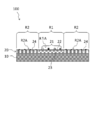
- FIG. 1 is a partial cross-sectional view schematically showing an optical panel according to an embodiment of the present invention.
- an optical panel 100 includes a base material 10 having translucency and an appearance layer 20 positioned on the base material 10.
- the material constituting the base material 10 is not limited as long as it has appropriate translucency. Examples of such materials include polyethylene terephthalate, polycarbonate, acrylic resin, and glass.
- the base material may be comprised from the laminated structure of the some member.
- the appearance layer 20 may be provided so as to be in direct contact with the base material 10, or even if an intervening layer exists between the base material 10 and the appearance layer 20. Good. Such an intervening layer should have an appropriate translucency similarly to the substrate 10.
- the appearance layer 20 includes a first region R1 having a relatively low reflectance of incident light from the appearance layer 20 side of the optical panel 100 and a second region R2 having a relatively high reflectance.
- the appearance layer 20 includes a first resin material and a second resin material.
- the surface R1A of the first region R1 includes a protruding point group 21 that is made of the first resin material and protrudes in the thickness direction of the appearance layer 20 to scatter external light.
- the specific composition of the first resin material and the second resin material is not limited.
- a polymer of an ionizing radiation polymerizable substance such as an acrylic resin or an epoxy resin may be contained.
- ionizing radiation can directly or indirectly ionize atoms and molecules such as light (including infrared rays, visible light, and ultraviolet rays), electromagnetic waves such as X-rays, and electrons. Mean radiation.
- the composition of the first resin material and the second resin material may be different or may be common.
- the first resin material includes a polymer of a first substance that is ionizing radiation polymerizable
- the second resin material includes a polymer of a second substance that is ionizing radiation polymerizable that is different from the first substance.
- the appearance layer 20 may contain a polymerization initiator.
- the polymerization initiator include photopolymerization initiators such as ⁇ -hydroxyalkylphenone and bis (2,4,6-trimethylbenzoyl) -phenylphosphine oxide.
- the second region R2 of the appearance layer 20 shown in FIG. 1 is composed of a layer 24 that is formed entirely of a mixed material of the first resin material and the second resin material in the thickness direction of the appearance layer 20.
- the thickness of the appearance layer 20 is not limited. Illustratively, the thickness of the appearance layer 20 may be 0.001 ⁇ m or more and 200 ⁇ m or less, and preferably 1 ⁇ m or more and 20 ⁇ m or less.
- the first region R1 of the outer layer 20 includes the protruding point group 21, the reflectance of incident light from the outer layer 20 side of the optical panel 100 is lower than the similar reflectance in the second region R2.
- the first region R1 of the appearance layer 20 may have a total light reflectance defined by JIS K7375: 2008 of 10% or less and preferably 5% or less.
- the filler component is an optional component.
- the proportion and arrangement of the size of the first region R1 in the entire appearance layer 20 and the proportion and arrangement of the size of the second region R2 in the entire appearance layer 20 should be appropriately set according to the application.
- the first region R1 is located in the center of the appearance layer 20 in plan view
- the second region R2 is located so as to surround the first region R1 in plan view.
- the appearance layer 20 may have a region other than the first region R1 and the second region R2.
- the surface (first region surface) R1A provided with the protruding point group 21 is rougher than the surface of the second region R2.
- the maximum height Rz of the surface roughness defined in JIS B0601: 2001 is preferably 0.5 ⁇ m or more, more preferably 1 ⁇ m or more. It is particularly preferable that the thickness is 5 ⁇ m or more.
- the upper limit of the surface roughness of the first region surface R1A is not limited, but if the surface roughness of the first region surface R1A is excessively large, the translucency of the optical panel 100 may be lowered.
- the total light transmittance specified in JIS 7375: 2008 is 50% or more (preferably 70% or more, more preferably 90% or more).
- the surface roughness of the first region surface R1A should be set so as to have a degree of translucency.
- the protruding point group 21 located on the first region surface R1A protrudes from the surface (second region surface) R2A of the second region R2.
- the protruding point group 21 By disposing the protruding point group 21 in this way, it may be possible to increase the degree of freedom of composition in a portion other than the protruding point group 21 of the appearance layer 20.
- the antireflection film described in Patent Document 1 has a structure in which fine particles are dispersed in a transparent resin, and by selectively removing the transparent resin, irregularities are formed on the surface, thereby preventing the reflection. A surface having a function is formed. Therefore, the surface of the region where the unevenness (corresponding to the protruding point group 21 of the appearance layer 20) is formed is inevitably depressed more than the surface of the region having no unevenness.
- the first region R1 and the second region R2 may have the same overall composition, and the composition distribution in the thickness direction of the appearance layer 20 may be different. In this case, as will be described later, it may be possible to form the first region R1 and the second region R2 by adjusting the process from a common member. In this case, the optical panel 100 is productive. Therefore, quality stability is also excellent.
- the composition of the first region R1 is different in the thickness direction of the external layer 20.
- the thickness direction of the appearance layer 20 it has at least a two-layer structure of the upper layer portion 22 (including the protruding point group 21. The same applies hereinafter) and the lower layer portion 23 on the substrate 10 side.
- the upper layer portion 22 is made of a first resin material
- the lower layer portion 23 is made of a second resin material. In the interface region between the upper layer portion 22 and the lower layer portion 23, both portions (the upper layer portion 22 and the lower layer portion 23) may be clearly separated as shown in FIG.
- the upper layer portion 22 may contain the first resin material as the main component and the second resin material to some extent
- the lower layer portion 23 may contain the second resin material as the main component and the first resin material to some extent. It may be. That is, in the first region R1, the ratio of the content of the first resin material in the upper layer portion 22 (the side opposite to the side facing the base material 10) to the content of the second resin material is lower layer portion 23 (base The ratio of the content of the first resin material on the side facing the material 10 to the content of the second resin material is higher.
- the appearance layer 20 of the optical panel 100 may further include a filler component or may not include a filler component.
- a filler component When the appearance layer 20 contains a filler component, a whitening phenomenon may occur in the appearance layer 20 because the adhesiveness between the filler component and the matrix component (resin component) changes over time. . Therefore, it may be preferable that the appearance layer 20 does not contain a filler component.
- the type of the filler component is not particularly limited.
- the filler component may be composed of an inorganic material such as silica, zirconia, and titania, or may be composed of an organic material such as a melamine resin.
- the filler component may contain both an organic material and an inorganic material.
- the particle size distribution of the filler component is also arbitrary. On the other hand, the layer corresponding to the appearance layer described in Patent Document 1 needs to precisely control the particle size distribution of the filler component as described above.
- the appearance layer 20 included in the optical panel according to the embodiment of the present invention described above includes the first region R1 including the protruding point group 21 and the second region R2 including no protruding point group. It is not limited. For example, the entire surface of the appearance layer 20 may include the protruding point group 21 or may include another region having optical characteristics different from those of the first region R1 and the second region R2.
- the manufacturing method of the optical panel including the appearance layer according to the embodiment of the present invention is not limited. If the manufacturing method described below is adopted, an optical panel according to an embodiment of the present invention can be efficiently manufactured.
- FIG. 2 is a flowchart showing a method for manufacturing an optical panel according to an embodiment of the present invention.
- An optical panel manufacturing method according to an embodiment of the present invention includes first to third steps described below, and further includes a fourth step and a fifth step.
- By performing the first step to the third step it is possible to manufacture an optical panel including an appearance layer having a protruding point group on the entire surface.
- By performing the first step to the fifth step it is possible to manufacture the optical panel 100 including the appearance layer 20 composed of the first region R1 and the second region R2 as shown in FIG.
- the case where the optical panel 100 shown in FIG. 1 is manufactured by performing the first step to the fifth step as shown in FIG. 2 is taken as a specific example.
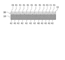
- FIG. 3 is a partial cross-sectional view schematically showing a manufacturing method (first step) of an optical panel according to an embodiment of the present invention.
- FIG. 4 is a partial cross-sectional view schematically showing a method for manufacturing an optical panel (second step) according to an embodiment of the present invention.
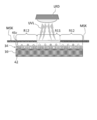
- FIG. 5 is a partial cross-sectional view schematically showing a method for manufacturing an optical panel (third step) according to an embodiment of the present invention.
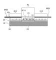
- FIG. 6 is a partial cross-sectional view schematically showing a method for manufacturing an optical panel (after the third step) according to an embodiment of the present invention.
- FIG. 7 is a partial cross-sectional view schematically showing a method for manufacturing an optical panel (fourth step) according to an embodiment of the present invention.
- FIG. 8 is a partial cross-sectional view schematically showing a method for manufacturing an optical panel (fifth step) according to an embodiment of the present invention.
- a liquid containing a second solvent that easily dissolves the second substance and has a boiling point higher than that of one solvent is prepared.
- the liquid material may not be composed of only the liquid, and may contain a filler component.
- Second material polyether-based acrylate resin
- Second solvent 1-propanol
- Each of the first substance, the first solvent, the second substance, and the second solvent may be composed of one kind of substance, or may be composed of a mixture of plural kinds of substances.
- the SP value of the first substance is close to the SP value of the first solvent
- the second substance can be easily dissolved in the second solvent.
- the first substance and the second substance are both acrylic resins such as acrylate resins and methacrylate resins
- the internal structure is changed (as examples of the internal structure, ether structure, polyester structure, urethane Structure, phenol structure, etc.), the SP value can be changed.
- the SP value may be changed by changing the molecular weight.
- the first solvent and the second solvent are mixed.
- a liquid material can be obtained by dissolving the first substance and the second substance in the mixed solvent.
- the first substance is dissolved in the first solvent to obtain the first solution
- the second substance is dissolved in the second solvent to obtain the second solution
- the first solution and the second solution are mixed. You may obtain a liquid by.
- the timing of adding the filler component is arbitrary.
- a liquid material is applied to one surface of the substrate 10 to form a coating film 30 on the substrate 10 (S101).
- a state in which the first substance 41 and the second substance 42 are dissolved in the mixed solvent 31 composed of the first solvent and the second solvent is shown as the first substance. 41 and the second substance 42 are represented by broken lines. Actually, the first substance 41 and the second substance 42 are not dissolved in the mixed solvent 31 in the coating film 30 and cannot be individually identified.
- the first substance 41 is deposited on the surface of the coating film to obtain a deposited coating film 34 (S102, FIG. 4).
- the method for volatilizing the first solvent 32 is not limited. As described above, since the first solvent 32 has a boiling point lower than that of the second solvent 33, if the coating film 30 on the substrate 10 is allowed to stand or is gently dried, the first solvent 32 starts from the mixed solvent 31 in the coating film 30. The solvent 32 is volatilized preferentially over the second solvent 33 and the content of the first solvent 32 in the coating film 30 is reduced.
- the first substance 41 is mainly dissolved in the first solvent 32, when the amount of the first solvent 32 in the coating film 30 decreases, the amount of the first substance 41 that can be dissolved in the coating film 30 decreases. As a result, as shown in FIG. 4, the first substance 40 becomes a precipitate 41 c and is located on the coating film 30, and the deposited coating film 34 is formed on the substrate 10.
- all the first solvents 32 contained in the mixed solvent 31 of the coating film 30 are volatilized, and all of the solvents in the deposited coating film 34 are composed of the second solvent 33, but are not limited thereto. .
- the first solvent 32 may remain to some extent in the solvent contained in the deposited coating film 34.
- all the 1st substances 41 contained in the coating film 30 become the precipitate 41c, it is not limited to this.
- a certain amount of the first substance 41 may be dissolved in the solvent of the deposited coating film 34.
- the precipitate 41c may positively contain a substance (third substance) other than the first substance 40.
- the first substance 41 and the second substance 42 located in the region irradiated with ionizing radiation are polymerized by irradiating at least a part of the deposited coating film 34 with ionizing radiation (S103, FIG. 5, FIG. 6).
- a mask MSK having an opening in a region corresponding to the first region R1 is used.
- the ionizing radiation (in this case, ultraviolet light) UVL from the light source LRD is applied to the first coating region R11, which is a partial region of the deposition coating 34, located in the opening of the mask MSK.
- the first substance 41 (at least a part of the precipitate 41c) and the second substance 42 located in the first coating film region R11 are polymerized, and the whole A first region R1 made of the first resin material and the second resin material is formed.
- the light source LRD and the mask MSK are arranged on the back side of the base material 10 (on the side opposite to the side on which the deposited coating 34 of the base material 10 is provided), and ionizing radiation is applied from the back side of the base material 10 (in the case of FIG. 5).
- UVL UVL
- the first coating 41 and the second coating 42 can be polymerized by irradiating the deposition coating 34 with ionizing radiation UVL that has passed through the substrate 10.
- the first region R1 shown in FIG. 6 has a different composition distribution in the thickness direction of the deposited coating film 34. Specifically, a portion (lower layer portion) 23 made of the second resin material formed from the second substance 42 is located on the substrate 10 side. Formed from the first substance 41, including the protruding point group 21 made of the first resin-based material formed from the precipitate 41 c of the first substance 41 on the side far from the base material 10 including the protruding point group 21. A portion (upper layer portion) 22 made of the first resin-based material is positioned.
- the surface R1A including the protruding point group 21 of the appearance layer 20 is formed by performing the third step.
- the third step if the entire coating film 34 is irradiated with ionizing radiation UVL without using the mask MSK, the appearance layer 20 having the protruding point group 21 on the entire surface can be formed from the coating film 34. .
- the second coating region R12 which is a region where the ionizing radiation UVL is not irradiated on the deposited coating 34, is heated to improve the surface smoothness of the second coating region R12 (S104, FIG. 7).
- the heating means is not limited.
- the second coating film region R ⁇ b> 12 is heated by a heating device HD that can heat the entire appearance layer 20.
- the first region R1 is also heated by the heating device HD, but since the polymerization reaction has already been completed in the first region R1, the shape of the protruding point group 21 is greatly changed by the heat from the heating device HD. Absent.
- the precipitate 41c is appropriately melted.
- the surface smoothness of the second coating film region R12 of the deposition coating 34 can be enhanced by diffusing into the deposition coating 34, while the first region R1 provided by the protruding point group 21 is roughened. It is possible to maintain the state.
- the liquid has compatibility with the first substance 41, and the precipitate 41c It is preferable to contain a third substance that promotes dissolution in the second solvent 33.
- the precipitate 41c formed in the second step includes the first substance 41 and the third substance.
- the third substance is selected so that the melting point of the precipitate 41c is lower than the melting point of the first substance precipitate. From this viewpoint, it is preferable that the melting point of the third substance is low.
- the melting point of the third substance is preferably not more than twice the melting point of the first substance 41, and more preferably not more than 1.5 times the melting point of the first substance 41. .
- the second region R2 of the appearance layer 20 formed from the deposited coating 34 located in the second coating region R12 poor appearance due to the non-uniformity of the appearance layer 20 such as fogging and glare is unlikely to occur.
- the cloudiness can be quantitatively evaluated by haze (JIS K7136: 2000).
- the third substance contained in the liquid remains in the appearance layer 20. Therefore, when the outer layer 20 contains the third substance, the second region R2 of the outer layer 20 is likely to have high surface smoothness, and is also caused by non-uniformity of the outer layer 20 such as cloudiness or glare. Appearance is unlikely to occur.
- the third substance has a functional group common to the functional group of the first substance 41, so that compatibility with the first substance 41 may be realized.
- the third substance when the first substance 41 has a hydroxyl group, the third substance also has a hydroxyl group, whereby compatibility with the first substance 41 can be realized.
- the third substance can be dissolved in the mixed solvent 31 or the first solvent 32 from the viewpoint of enhancing the handleability and enhancing the uniformity of the coating film 30 and the appearance layer 20.
- the amount of addition based on the sum of the mass of the first substance 41 of the third substance and the mass of the second substance 42 is not limited. As long as the uniformity of the coating film 30 and the appearance layer 20 can be ensured, the higher the amount of the third substance added, the lower the melting point of the precipitate 41c, which is preferable.
- Examples of the third substance having a hydroxyl group include a phenolic compound (a compound having a site in which a hydroxyl group is bonded to an aromatic ring), and a phenolic compound having a melting point of 100 ° C. or lower is a preferred example. More preferred examples include a series compound, and a hindered phenol compound having a melting point of 100 ° C. or lower can be mentioned as a particularly preferred example. As a specific example of such a hindered phenol compound having a melting point of 100 ° C. or lower, octadecyl 3- (3,5-di-tert-butyl-4-hydroxyphenyl) propionate used in Examples described later is used. , Butylhydroxyanisole, 2,6-di-tert-butyl-4-methylphenol, and 4-tert-butylphenol.
- the second coating film region R12 in which the surface smoothness is improved by the execution of the fourth step is irradiated with the ionizing radiation UVL from the light source LRD, thereby being positioned in the second coating film region R12.
- the first substance 41 and the second substance 42 are polymerized to form a second region R2 made of the first resin material and the second resin material (S105, FIG. 8).
- the optical panel 100 including the appearance layer 20 having the first region R1 and the second region R2 is manufactured.
- the conditions of irradiation with ionizing radiation UVL from the light source LRD performed in the second step and the fifth step are the size of the irradiation region, the types of the first substance 41 and the second substance 42, the thickness of the deposited coating film 34, and the like. It should be set as appropriate in consideration.
- the protruding point group 21 that directly performs the antireflection function is made of the resin-based material. Therefore, whether or not the liquid material contains the filler component and the appearance layer 20 has the antireflection function. It can be set independently whether it has or not. Therefore, the liquid material may further include a filler component or may not include a filler component.
- the liquid material may contain a polymerization initiator.
- the polymerization of the first substance 41 and the second substance 42 can be performed by irradiation with electromagnetic waves such as ultraviolet light.
- electromagnetic waves such as ultraviolet light.
- Specific examples of the polymerization initiator are as described above.
- the fourth step heating is performed so that the precipitate 41c of the first substance 41 deposited in the deposited coating film 34 is melted, but the present invention is not limited to this.
- the precipitation coating 34 is heated, so that the solubility of the precipitate 41 c of the first substance 41 in the second solvent 33 is increased, and the first substance 41 is dissolved in the second solvent 33, whereby the precipitate 41c may disappear and the surface smoothness of the deposited coating film 34 may increase.
- a device includes the optical panel 100 according to the above-described embodiment of the present invention.
- Specific examples of such devices include portable information terminals such as smartphones, mobile phones, and notebook computers; image display devices such as TVs and car navigation systems; instrument panels (instrument panels) of moving bodies such as automobiles and airplanes, console panels, and the like. Can be mentioned. Since the device according to an embodiment of the present invention includes the optical panel 100 having an antireflection function, the display image has excellent visibility.
- the appearance layer 20 of the optical panel 100 can be used as a transfer layer having a transfer source surface for forming a transfer surface on a transfer object.
- a transfer surface that is the reverse surface of the transfer original surface can be formed on the transfer object.
- the transfer layer includes a first resin material containing a polymer of an ionizing radiation polymerizable first substance, and a second resin containing a polymer of an ionizing radiation polymerizable second substance different from the first substance.
- the transfer source surface includes a resin-based material, and includes a protruding point group that is made of the first resin-based material and protrudes in the thickness direction of the transfer layer and scatters external light.
- the composition differs in the layer thickness direction, and the ratio of the content of the first resin material on the transfer source surface side to the content of the second resin material is the first resin system on the side opposite to the transfer source surface side. It is higher than the ratio of the content of the material to the content of the second resin material.
- the transfer body may include a third substance having compatibility with the first substance. Since the other characteristics of the transfer layer are the same as those of the appearance layer 20, the description thereof is omitted.
- the transfer body can be manufactured by the same manufacturing method as that of the optical panel 100.
- a manufacturing method includes an ionizing radiation polymerizable first substance, an ionizing radiation polymerizable second substance different from the first substance, a first solvent that dissolves the first substance more easily than the second substance, A liquid material containing a second solvent that is easier to dissolve the second substance than the substance and has a higher boiling point than the first solvent is applied to one surface of the substrate to form a coating film on the substrate.
- a third step of polymerizing the first substance and the second substance located in the region irradiated with the ionizing radiation by irradiating the ionizing radiation to the region of the portion, and the transfer source including the protruding point group by the third step A surface is formed.
- the base material does not need to have translucency.
- the surface of the substrate on which the liquid material is applied need not be a flat surface, but a flat surface is preferable from the viewpoint of increasing the uniformity of the thickness of the coating film.
- the substrate may not be a constituent element of the transfer body. That is, when a transfer layer having a transfer source surface is formed after the third step, the transfer layer is peeled off from the substrate, and the transfer layer alone or a surface opposite to the surface on which the transfer source surface is located is separated. A transfer body provided with the member and a transfer layer may be obtained so as to face the member.
- the transfer layer is composed of a first region having a surface having a protruding point group and a second region having a surface not having the protruding point group.
- heating may be performed so that the precipitate containing the first substance in the deposited coating is melted.
- the liquid body contains a third substance having compatibility with the first substance
- the precipitate containing the first substance formed in the second step contains the third substance
- the precipitate containing the first substance Is preferably lower in melting point than the precipitate made of the first substance.
- the following materials were prepared as the first substance, the first solvent, the second substance, and the second solvent.
- the first substance and the second substance are acrylic resins, and the SP values as the substances are made different from each other by changing the structure (ether structure, polyester structure, urethane structure, phenol structure, etc.) in the inside. It is set.
- the melting point of the first substance was 48 ° C.
- Multifunctional acrylate resin penentaerythritol triacrylate
- 1st solvent Methyl isobutyl ketone
- 2nd substance Polyether-type acrylate resin (It is a urethane prepolymer which has a phenyl group, and has SP value 1.2 times with respect to SP value of polyfunctional acrylate resin.)
- Second solvent 1-propanol (having an SP value of 1.37 times that of methyl isobutyl ketone)
- the first substance 15g was dissolved in 50 mL of the first solvent to obtain a first solution, and the second substance 15g was dissolved in 50 mL of the second solvent to obtain a second solution.
- 50 mL of 1st solution and 50 mL of 2nd solution were mixed, and the polymerization initiator was further added (addition amount: 2 mass% with respect to solid content), and the mixed solution was obtained.
- the polymerization initiator used was one of the following two types (see Table 1).
- Polymerization initiator 1 Ketone-based polymerization initiator ("Irgacure 184" manufactured by BASF)
- Polymerization initiator 2 Phosphine oxide polymerization initiator ("Irgacure 819" manufactured by BASF)
- the liquid material made of the obtained mixed solution was applied onto a substrate made of polycarbonate to obtain a coating film (first step).
- the thickness of the coating film immediately after coating was about 10 ⁇ m.
- the first solvent was generally volatilized by leaving it for about 1 minute, and the first substance in the coating film was deposited on the substrate. A deposited coating was obtained (second step).
- a mask having an opening in an area corresponding to the view area is prepared, placed on the deposited coating film, the first coating film area exposed by the opening is irradiated with ultraviolet light from a light source, and the first coating film area is exposed.
- a first region was formed (third step).
- the type of light source used, illuminance (unit: mW / cm 2 ), and integrated dose (unit: mJ / cm 2 ) were as shown in Table 1.
- the deposited coating film having a partially polymerized region (first region) is heated (80 ° C., 10 minutes), and in an unpolymerized region. A precipitate of the first substance existing in a certain second coating film region was melted to increase the surface smoothness of the second coating film region (fourth step).
- the entire region was irradiated with ultraviolet light from a light source to form a second region from the second coating region, and an appearance layer was obtained on the substrate (fifth step).
- the type of light source used, illuminance (unit: mW / cm 2 ), and integrated dose (unit: mJ / cm 2 ) were as shown in Table 1.
- the roughness (the maximum height Rz of the surface roughness defined in JIS B0601: 2001) of the first region and the second region of the appearance layer obtained was measured. The results are shown in Table 2. Further, based on the difference between the roughness of the first region and the roughness of the second region, an evaluation was made as to whether or not an appearance layer partially having an antireflection function could be produced. The evaluation results are shown in Table 2. Specifically, when the maximum height Rz of the surface roughness in the first region is 0.5 ⁇ m or more larger than the maximum height Rz of the surface roughness in the roughness of the second region, the antireflection function. It was judged that an appearance layer having a part of the surface could be made ("A" in Table 2), and if the above difference was less than 0.5 ⁇ m, a part having an antireflection function was made. ("B" in Table 2).
- the protruding point group is appropriately formed, and the protruding point group is maintained even by subsequent heating. It was confirmed. It is also confirmed that the second region formed from the second coating region can be made a smooth surface by appropriately dissolving the precipitate of the first substance formed in the second coating region by heating. It was done. That is, it was confirmed that by performing the manufacturing method according to one embodiment of the present invention, an appearance layer having an antireflection function region and a highly reflective region can be manufactured.
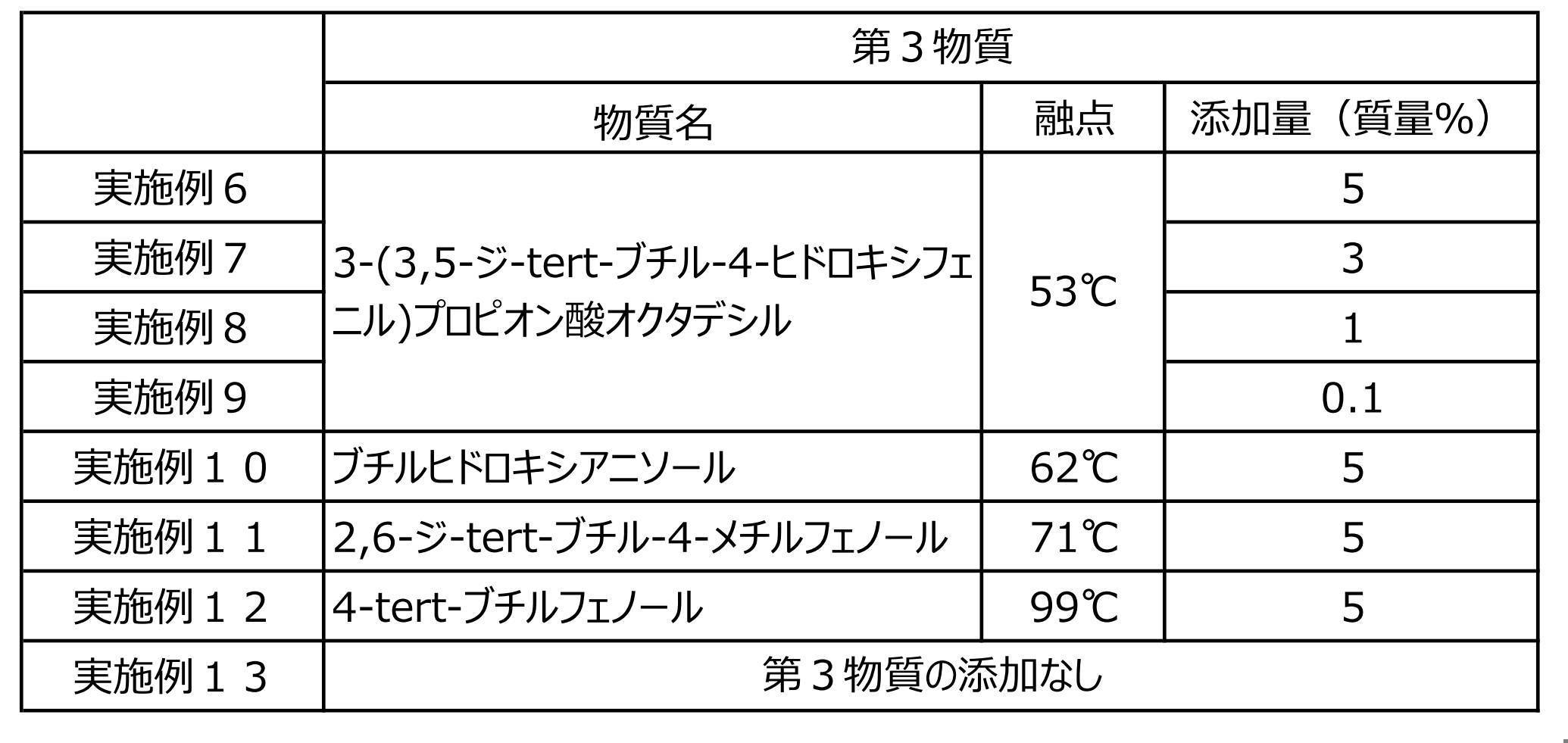
- Example 6 to Example 13 25 g of the first substance used in Example 1 was dissolved in 50 mL of the first solvent to obtain a first solution, and 25 g of the second substance was dissolved in 50 mL of the second solvent to obtain a second solution. 50 mL of the first solution and 50 mL of the second solution are mixed, and further, a ketone polymerization initiator (“Irgacure 184” manufactured by BASF) is added as a polymerization initiator by 2 mass% with respect to the solid content, and the mixed solution is Obtained. To this mixed solution, the third substance was added in an addition amount (unit: mass%) shown in Table 3 based on the sum of the mass of the first substance and the mass of the second substance.
- a ketone polymerization initiator (“Irgacure 184” manufactured by BASF)
- the substance names and melting points of the third substances according to the respective examples are as shown in Table 3. Since the third substance has a hydroxyl group and is common to the first substance in that it has a hydroxyl group, the third substance is compatible with the first substance. Therefore, the precipitate formed using the liquid material to which the third substance is added includes the first substance and the third substance.
- An appearance layer having a first region and a second region was formed on the substrate in the same manner as in Example 1 except that the thickness of the coating film immediately after coating was set to 14 ⁇ m using a # 12 bar coater.
Landscapes
- Physics & Mathematics (AREA)
- Chemical & Material Sciences (AREA)
- General Physics & Mathematics (AREA)
- Optics & Photonics (AREA)
- Health & Medical Sciences (AREA)
- General Chemical & Material Sciences (AREA)
- Toxicology (AREA)
- Chemical Kinetics & Catalysis (AREA)
- Medicinal Chemistry (AREA)
- Polymers & Plastics (AREA)
- Organic Chemistry (AREA)
- Laminated Bodies (AREA)
- Optical Elements Other Than Lenses (AREA)
- Surface Treatment Of Optical Elements (AREA)
Abstract
反射防止機能を果たすために微粒子の存在を必須としない光学パネル100として、透光性を備えた基材10と、基材10の上に位置する外観層20とを備え、外観層20は、光学パネル100の外観層20側からの入射光の反射率が相対的に低い第1領域R1および反射率が相対的に高い第2領域R2を備え、外観層20は、第1樹脂系材料および第2樹脂系材料を含み、第1領域R1の面R1Aは、第1樹脂系材料からなり外観層の厚さ方向に突出して外光を散乱する突出点群21を備える光学パネル100が提供される。
Description
本発明は、光学パネルおよびその製造方法ならびに上記の光学パネルを備える機器に関する。
特許文献1には、透明基材上に積層される反射防止膜であって、前記反射防止膜が、透明樹脂と該透明樹脂中に分散された微粒子とからなり、前記微粒子の最近接粒子同士の中心間の平均距離が50~800nmの範囲にあり、前記反射防止膜中の前記微粒子の配列構造がアモルファス構造であり、且つ、前記反射防止膜の表面に凸部の平均高さが40~500nmの範囲にある凹凸形状が形成されていること、を特徴とする反射防止膜が開示されている。
特許文献1に記載される反射防止膜は、膜中に分散された微粒子が反射防止膜の面に凹凸を作り、この凹凸によって外光を散乱して反射防止が行われている。そして、この凹凸を形成するために、微粒子が分散するマトリックス材料を選択的に除去する加工が行われている。すなわち、特許文献1に記載される反射防止膜は、マトリックス材料とこの材料とは除去加工性が十分に異なる微粒子との存在が不可欠である。このため、反射防止膜中に微粒子を存在させることを望まない場合には、特許文献1に記載される反射防止膜を用いることができない。また、反射防止膜中に微粒子を存在させることを望む場合であっても、このマトリックス材料とは除去加工性が十分に異なる微粒子の存在が必須となるため、微粒子の選択自由度が著しく低くなる。
本発明は、反射防止機能を果たすために微粒子の存在を必須としない光学パネルを提供することを目的とする。本発明は、かかる光学パネルの製造方法および上記の光学パネルを備える機器を提供することも目的とする。
上記の課題を解決するために提供される本発明は、一態様において、透光性を備えた基材と、前記基材の上に位置する外観層とを備える光学パネルであって、前記外観層は、前記光学パネルの前記外観層側からの入射光の反射率が相対的に低い第1領域および前記反射率が相対的に高い第2領域を備え、前記外観層は、第1樹脂系材料および第2樹脂系材料を含み、前記第1領域の面は、前記第1樹脂系材料からなり前記外観層の厚さ方向に突出して外光を散乱する突出点群を備えることを特徴とする光学パネルである。
上記の本発明に係る光学パネルは、樹脂系材料からなる突出点群によって外光を散乱させる反射防止機能を実現している。したがって、外観層が微粒子を含有することは、反射防止機能の発現と切り離されている。それゆえ、外観層の組成の設計自由度を高めることが可能である。
上記の光学パネルにおいて、前記第1領域は前記外観層の厚さ方向に組成が相違していてもよい。この場合において、前記基材に対向する側とは反対側における前記第1樹脂系材料の含有量の前記第2樹脂系材料の含有量に対する比は、前記基材に対向する側における前記第1樹脂系材料の含有量の前記第2樹脂系材料の含有量に対する比よりも高くてもよい。
上記の光学パネルにおいて、前記突出点群は、前記第2領域の面よりも突出していてもよい。
上記の光学パネルにおいて、前記第1領域と前記第2領域とは、全体組成が等しく、前記外観層の厚さ方向の組成分布が相違していてもよい。この場合には、第1領域と第2領域とで外観層を形成するための材料を共通なものとしておいて、異なったプロセスを実施することによって第1領域と第2領域とを作り分けることができる。
本発明は、他の一態様として、透光性を備えた基材と、前記基材の上に位置する外観層とを備える光学パネルを提供する。かかる光学パネルにおいては、前記外観層は、第1樹脂系材料および第2樹脂系材料を含み、前記外観層の面は、少なくとも一部の領域において、前記第1樹脂系材料からなり前記外観層の厚さ方向に突出して外光を散乱する突出点群を備える。
かかる光学パネルも、上記の第1領域および第2領域を備える光学パネルと同様に、外観層の組成の設計自由度を高めることが可能である。
上記の光学パネルにおいて、前記突出点群を備える領域は前記外観層の厚さ方向に組成が相違していてもよい。この場合において、前記基材に対向する側とは反対側における前記第1樹脂系材料の含有量の前記第2樹脂系材料の含有量に対する比は、前記基材に対向する側における前記第1樹脂系材料の含有量の前記第2樹脂系材料の含有量に対する比よりも高くてもよい。
上記の光学パネルにおいて、前記外観層はフィラー成分をさらに含んでもよいし、前記外観層はフィラー成分を含まなくてもよい。
上記の光学パネルにおいて、前記第1樹脂系材料は電離放射線重合性の第1物質の重合体を含んでいてもよく、前記第2樹脂系材料は、前記第1物質とは異なる電離放射線重合性の第2物質の重合体を含んでいてもよい。この場合において、前記外観層は重合開始剤をさらに含んでいてもよい。また、前記第1物質に対する相溶性を有する第3物質を含んでいてもよい。第3物質はフェノール系化合物が好ましく、融点が100℃以下のフェノール系化合物がさらに好ましく、ヒンダードフェノール系化合物が特に好ましい。第3物質を含むことにより、第2領域の平滑性や光学特性が高まることもある。
本発明は、他の一態様として、透光性を有する基材と、前記基材の上に位置して外光を散乱する突出点群を備える面を有する外観層とを備える光学パネルの製造方法を提供する。かかる製造方法は、電離放射線重合性の第1物質と、前記第1物質とは異なる電離放射線重合性の第2物質と、前記第2物質よりも前記第1物質を溶解しやすい第1溶媒と、前記第1物質よりも前記第2物質を溶解しやすく前記第1溶媒よりも沸点が高い第2溶媒と、を含有する液状体を、前記基材の一方の面に塗布して前記基材上に塗膜を形成する第1ステップ;前記塗膜に含有される前記第1溶媒を揮発させることにより、前記第1物質を含む析出体を前記塗膜の表面に位置させて析出塗膜を得る第2ステップ;および前記析出塗膜の少なくとも一部の領域に電離放射線を照射することにより、前記電離放射線が照射された領域に位置する前記第1物質および前記第2物質を重合させる第3ステップを備え、前記第3ステップにより、前記外観層の前記突出点群を備える面が形成されることを特徴とする。
このような製造方法により外観層を形成することにより、反射防止機能を有する外観層を、組成上の制約少なく、特にフィラー成分の含有を必須とすることなく製造することができる。
上記の製造方法において、前記第3ステップでは、前記析出塗膜の全体に前記電離放射線を照射することにより、前記突出点群を全面に備える前記外観層を前記析出塗膜から形成してもよい。かかる製造方法を採用することにより、全面に反射防止機能を有する外観層を製造することができる。
上記の製造方法において、前記外観層は、前記突出点群を備える面を有する第1領域と、前記突出点群を備えない面を有する第2領域とからなり、前記第3ステップでは、前記析出塗膜の一部の領域である第1塗膜領域について前記電離放射線を照射することにより、前記第1塗膜領域に位置する前記第1物質および前記第2物質を重合させて、前記第1領域を形成し、前記第3ステップに続いて、前記析出塗膜における前記電離放射線が照射されていない第2塗膜領域を加熱して、前記第2塗膜領域の面平滑性を高める第4ステップ;および前記面平滑性が高められた第2塗膜領域に電離放射線を照射することにより、前記第2塗膜領域に位置する前記第1物質および前記第2物質を重合させて、前記第2領域を形成する第5ステップを備えてもよい。かかる製造方法を採用することにより、反射防止機能を有する第1領域と反射防止機能を有しない第2領域とを備える外観層を製造することができる。
上記の製造方法において、前記液状体はフィラー成分をさらに含んでいてもよい。この場合には、外観層はフィラー成分を含有するものとなる。上記の製造方法において、前記液状体はフィラー成分を含まなくてもよい。この場合には、外観層はフィラー成分を含有しないものとなる。このように、液状体の組成を変化させることによって、外観層がフィラー成分を含有するか否かを設定することができる。
上記の製造方法において、前記液状体は重合開始剤を含んでいてもよい。この場合には、前記第1物質および前記第2物質の重合を、可視光や紫外光などの電磁波の照射により行うことができる。
上記の製造方法において、前記第4ステップでは、前記析出塗膜における前記第1物質の析出体が溶融するように加熱を行ってもよい。析出塗膜では第1物質の析出体により析出塗膜の表面が粗面化していることから、この第1物質の析出体を溶解することにより、表面の平滑性を高めることができる。
前記液状体は前記第1物質に対する相溶性を有する第3物質を含有していてもよい。この場合において、前記第2ステップで形成される前記第1物質を含む析出体は前記第3物質を含み、前記第1物質を含む析出体は前記第1物質からなる析出体よりも融点が低いことが好ましい。第3物質はフェノール系化合物が好ましく、融点が100℃以下のフェノール系化合物がさらに好ましく、ヒンダードフェノール系化合物が特に好ましい。第3物質を含むことにより、第2領域の平滑性や光学特性が高まることもある。
本発明は、別の一態様として、上記の本発明の一態様に係る光学パネルを備える機器を提供する。
本発明は、また別の一態様として、転写元面を有する転写層を備える転写体を提供する。かかる転写体において、前記転写層は、電離放射線重合性の第1物質の重合体を含む第1樹脂系材料、および前記第1物質とは異なる電離放射線重合性の第2物質の重合体を含む第2樹脂系材料を含み、前記転写元面は、前記第1樹脂系材料からなり前記転写層の厚さ方向に突出して外光を散乱する突出点群を備え、前記転写層における前記転写元面を含む領域は、前記転写層の厚さ方向に組成が相違し、前記転写元面側における前記第1樹脂系材料の含有量の前記第2樹脂系材料の含有量に対する比は、前記転写元面側とは反対側における前記第1樹脂系材料の含有量の前記第2樹脂系材料の含有量に対する比よりも高い。このように、上記の本発明に係る光学パネルの外観層を、被転写物に転写面を形成するための転写元面を有する転写層として用いることが可能である。上記の転写体において、前記第1物質に対する相溶性を有する第3物質を含んでいてもよい。第3物質はフェノール系化合物が好ましく、融点が100℃以下のフェノール系化合物がさらに好ましく、ヒンダードフェノール系化合物が特に好ましい。
本発明は、また別の一態様として、外光を散乱する突出点群を備える転写元面を有する転写層を備える転写体の製造方法を提供する。かかる製造方法は、電離放射線重合性の第1物質と、前記第1物質とは異なる電離放射線重合性の第2物質と、前記第2物質よりも前記第1物質を溶解しやすい第1溶媒と、前記第1物質よりも前記第2物質を溶解しやすく前記第1溶媒よりも沸点が高い第2溶媒と、を含有する液状体を、基材の一方の面に塗布して前記基材上に塗膜を形成する第1ステップ;前記塗膜に含有される前記第1溶媒を揮発させることにより、前記第1物質を含む析出体を前記塗膜の表面に位置させて析出塗膜を得る第2ステップ;および前記析出塗膜の少なくとも一部の領域に電離放射線を照射することにより、前記電離放射線が照射された領域に位置する前記第1物質および前記第2物質を重合させる第3ステップを備え、前記第3ステップにより、前記突出点群を備える前記転写元面が形成される。
上記の転写体の製造方法において、前記転写層は、前記突出点群を備える面を有する第1領域と、前記突出点群を備えない面を有する第2領域とからなり、前記第3ステップでは、前記析出塗膜の一部の領域である第1塗膜領域について前記電離放射線を照射することにより、前記第1塗膜領域に位置する前記第1物質および前記第2物質を重合させて、前記第1領域を形成し、前記第3ステップに続いて、前記析出塗膜における前記電離放射線が照射されていない第2塗膜領域を加熱して、前記第2塗膜領域の面平滑性を高める第4ステップ;および前記面平滑性が高められた第2塗膜領域に電離放射線を照射することにより、前記第2塗膜領域に位置する前記第1物質および前記第2物質を重合させて、前記第2領域を形成する第5ステップを備えていてもよい。かかる製造方法によれば、転写層の転写元面が位置する面に平滑性に優れる面を設けることができる。
上記の転写体の製造方法において、前記第4ステップでは、前記析出塗膜における前記第1物質を含む析出体が溶融するように加熱を行ってもよい。この場合において、前記液状体は前記第1物質に対する相溶性を有する第3物質を含有し、前記第2ステップで形成される前記第1物質を含む析出体は前記第3物質を含み、前記第1物質を含む析出体は前記第1物質からなる析出体よりも融点が低いことが好ましい。第3物質はフェノール系化合物が好ましく、融点が100℃以下のフェノール系化合物がさらに好ましく、ヒンダードフェノール系化合物が特に好ましい。
本発明によれば、反射防止機能を果たすために微粒子の存在を必須としない光学パネル、かかる光学パネルの製造方法および上記の光学パネルを備える機器が提供される。
以下、本発明の実施の形態について図面を参照しつつ説明する。なお、各図面中、同様の構成要素には同一の符号を付して詳細な説明は適宜省略する。
図1は、本発明の一実施形態に係る光学パネルを模式的に示す部分断面図である。
図1に示されるように、本発明の一実施形態に係る光学パネル100は、透光性を備えた基材10と、基材10の上に位置する外観層20とを備える。
基材10を構成する材料は適切な透光性を有する限り、限定されない。かかる材料として、ポリエチレンテレフタレート、ポリカーボネート、アクリル樹脂、ガラスなどが例示される。基材は、複数の部材の積層構造体から構成されていてもよい。
外観層20は、図1に示されるように、基材10に直接的に接するように設けられていてもよいし、基材10と外観層20との間に介在層が存在していてもよい。かかる介在層は、基材10と同様に、適切な透光性を有するべきである。
外観層20は、光学パネル100の外観層20側からの入射光の反射率が相対的に低い第1領域R1および反射率が相対的に高い第2領域R2を備える。外観層20は、第1樹脂系材料および第2樹脂系材料を含む。第1領域R1の面R1Aは、第1樹脂系材料からなり外観層20の厚さ方向に突出して外光を散乱する突出点群21を備える。
第1樹脂系材料および第2樹脂系材料の具体的な組成は限定されない。アクリル系樹脂、エポキシ系樹脂など電離放射線重合性の物質の重合体を含有していてもよい。本明細書において、「電離放射線」とは、光(赤外線、可視光、および紫外線を含む。)、X線等の電磁波および電子など、原子・分子を直接的または間接的に電離させることが可能な放射線を意味する。
第1樹脂系材料と第2樹脂系材料とは組成が異なっていてもよいし、共通であってもよい。一具体例として、第1樹脂系材料は電離放射線重合性の第1物質の重合体を含み、第2樹脂系材料は、第1物質とは異なる電離放射線重合性の第2物質の重合体を含む。この場合において、外観層20は、重合開始剤を含有していてもよい。重合開始剤の具体例として、α‐ヒドロキシアルキルフェノン、ビス(2,4,6‐トリメチルベンゾイル)‐フェニルフォスフィンオキサイドなどの光重合開始剤が挙げられる。
図1に示される外観層20の第2領域R2は、外観層20の厚さ方向の全体が第1樹脂系材料と第2樹脂系材料との混合材料からなる層24からなる。
外観層20の厚さは限定されない。例示的に示せば、外観層20の厚さは、0.001μm以上200μm以下であり、1μm以上20μm以下であることが好ましい場合がある。
外観層20の第1領域R1は、突出点群21を備えるため、光学パネル100の外観層20側からの入射光の反射率が、第2領域R2における同様の反射率よりも低い。具体的には、外観層20の第1領域R1は、JIS K7375:2008に規定される全光線反射率が、10%以下であって、5%以下であることが好ましい場合がある。
後述するように、外観層20において、フィラー成分は任意的な含有成分である。
第1領域R1の外観層20全体における大きさの割合および配置、ならびに第2領域R2の外観層20全体における大きさの割合および配置は、用途に応じて適宜設定されるべきものである。図1に示される光学パネル100では、第1領域R1は、平面視で外観層20の中央部に位置し、第1領域R1を平面視で囲むように第2領域R2が位置しているが、これに限定されない。第1領域R1および第2領域R2以外の領域を外観層20が有していてもよい。
第1領域R1は突出点群21において外光を散乱させることから、突出点群21を備える面(第1領域面)R1Aは第2領域R2の面よりも粗な面となる。具体的には、第1領域面R1Aは、JIS B0601:2001において規定される表面粗さの最大高さRzが、0.5μm以上であることが好ましく、1μm以上であることがより好ましく、1.5μm以上であることが特に好ましい。第1領域面R1Aの表面粗さの上限は限定されないが、第1領域面R1Aの表面粗さが過度に大きい場合には、光学パネル100の透光性が低下してしまう場合がある。光学パネル100は、基材10がプラスチックからなる場合を例とすると、JIS 7375:2008に規定される全光線透過率が50%以上(好ましくは70%以上、より好ましくは90%以上)となる程度の透光性を有するように、第1領域面R1Aの表面粗さは設定されるべきである。
図1に示されるように、第1領域面R1Aに位置する突出点群21は、第2領域R2の面(第2領域面)R2Aよりも突出している。このように突出点群21が配置されることにより、外観層20の突出点群21以外の部分における組成の自由度を高めることが可能となる場合がある。例えば、特許文献1に記載される反射防止膜は、透明樹脂中に微粒子が分散された構造を有し、透明樹脂が選択的に除去されることにより、表面に凹凸を形成して、反射防止機能を有する面が形成されている。したがって、凹凸(外観層20の突出点群21に相当する。)が形成されている領域の表面は、凹凸を有しない領域の表面をよりも必然的に窪んでしまう。
第1領域R1と第2領域R2とは、全体組成が等しく、外観層20の厚さ方向の組成分布が相違していてもよい。この場合には、後述するように、共通の部材からプロセスを調整することにより第1領域R1および第2領域R2を形成することが可能な場合があり、この場合には光学パネル100は生産性に優れ、それゆえ、品質安定性にも優れる。
図1に示される光学パネル100が備える外観層20では、第1領域R1は外観層20の厚さ方向に組成が相違する。具体的には、外観層20の厚さ方向において、表面側の上層部分22(突出点群21を含む。以下同じ。)と、基材10側の下層部分23との少なくとも2層構造を有する。上層部分22は第1樹脂系材料からなり、下層部分23は第2樹脂系材料からなる。上層部分22と下層部分23との界面領域では、図1に示されるように両部分(上層部分22、下層部分23)が明確に分離していてもよいし、第1樹脂系材料および第2樹脂系材料を含む層(この層は外観層20の厚さ方向に組成が変化していてもよい。)を有していてもよい。上層部分22は第1樹脂系材料を主成分とし第2樹脂系材料をある程度含有していてもよいし、下層部分23は第2樹脂系材料を主成分とし第1樹脂系材料をある程度含有していてもよい。すなわち第1領域R1では、上層部分22(基材10に対向する側とは反対側)における第1樹脂系材料の含有量の第2樹脂系材料の含有量に対する比は、下層部分23(基材10に対向する側)における記第1樹脂系材料の含有量の前記第2樹脂系材料の含有量に対する比よりも高い。
本発明の一実施形態に係る光学パネル100の外観層20は、フィラー成分をさらに含んでいてもよいし、フィラー成分を含まなくてもよい。外観層20がフィラー成分を含有する場合には、フィラー成分とマトリックス成分(樹脂成分)との間の密着性が経時的に変化するなどの理由により、外観層20に白化現象が生じる場合がある。したがって、外観層20はフィラー成分を含有しないことが好ましい場合もある。外観層20がフィラー成分を含有する場合において、フィラー成分の種類は特に限定されない。フィラー成分はシリカ、ジルコニア、チタニアのような無機系材料から構成されていてもよいし、メラミン樹脂のような有機系材料から構成されていてもよい。フィラー成分は有機系材料と無機系材料との双方を含有していてもよい。また、フィラー成分の粒径分布も任意である。これに対し、特許文献1に記載される外観層に相当する層は、前述のように、フィラー成分の粒径分布を精密に制御する必要がある。
以上説明した本発明の一実施形態に係る光学パネルが備える外観層20は、突出点群21を備える第1領域R1と突出点群を備えない第2領域R2とから構成されるが、これに限定されない。例えば、外観層20の全面が突出点群21を備えていてもよいし、第1領域R1および第2領域R2とは光学的な特性が異なる他の領域を備えていてもよい。
本発明の一実施形態に係る外観層を備える光学パネルの製造方法は限定されない。次に説明する製造方法を採用すれば、本発明の一実施形態に係る光学パネルを効率的に製造することができる。
図2は、本発明の一実施形態に係る光学パネルの製造方法を示すフローチャートである。本発明の一実施形態に係る光学パネルの製造方法は、次に説明する第1ステップから第3ステップを備え、さらに、第4ステップおよび第5ステップを備える。第1ステップから第3ステップを実施することにより、全面に突出点群を有する外観層を備える光学パネルを製造することが可能である。第1ステップから第5ステップを実施することにより、図1に示されるような第1領域R1および第2領域R2から構成される外観層20を備える光学パネル100を製造することができる。以下の説明では、図2に示されるように第1ステップから第5ステップを実施して、図1に示される光学パネル100を製造する場合を具体例とする。
図3は、本発明の一実施形態に係る光学パネルの製造方法(第1ステップ)を模式的に示す部分断面図である。図4は、本発明の一実施形態に係る光学パネルの製造方法(第2ステップ)を模式的に示す部分断面図である。図5は、本発明の一実施形態に係る光学パネルの製造方法(第3ステップ)を模式的に示す部分断面図である。図6は、本発明の一実施形態に係る光学パネルの製造方法(第3ステップ後)を模式的に示す部分断面図である。図7は、本発明の一実施形態に係る光学パネルの製造方法(第4ステップ)を模式的に示す部分断面図である。図8は、本発明の一実施形態に係る光学パネルの製造方法(第5ステップ)を模式的に示す部分断面図である。
まず、電離放射線重合性の第1物質と、第1物質とは異なる電離放射線重合性の第2物質と、第2物質よりも第1物質を溶解しやすい第1溶媒と、第1物質よりも前記第2物質を溶解しやすく1溶媒よりも沸点が高い第2溶媒と、を含有する液状体を用意する。この液状体の組成の具体例は次のとおりである。液状体は液体のみから構成されていなくてもよく、フィラー成分を含有していてもよい。
第1物質:多官能アクリレート樹脂
第1溶媒:メチルイソブチルケトン
第2物質:ポリエーテル系アクリレート樹脂
第2溶媒:1-プロパノール
第1物質:多官能アクリレート樹脂
第1溶媒:メチルイソブチルケトン
第2物質:ポリエーテル系アクリレート樹脂
第2溶媒:1-プロパノール
第1物質、第1溶媒、第2物質および第2溶媒のそれぞれは、一種類の物質から構成されていてもよいし、複数種類の物質の混合体から構成されていてもよい。第1物質のSP値と第1溶媒のSP値とが近くなるように設定することにより、第1物質を第1溶媒に溶解しやすくすることができる。第2物質のSP値と第2溶媒のSP値とが近くなるように設定することにより、第2物質を第2溶媒に溶解しやすくすることができる。例えば、第1物質および第2物質が、いずれもアクリレート樹脂やメタクリレート樹脂のようなアクリル系樹脂であっても、内部構造を変化させること(内部構造の具体例として、エーテル構造、ポリエステル構造、ウレタン構造、フェノール構造などが挙げられる。)により、SP値を変化させることができる。同じような構造を有する材料であっても、分子量を変化させることによってSP値を変化させることができる場合もある。
上記のように各成分のSP値を設定するとともに、さらに、第1溶媒のSP値と第2溶媒のSP値とが大きく異ならないように設定すれば、第1溶媒と第2溶媒とが混和してなる混合溶媒に第1物質および第2物質を溶解させることにより液状体を得ることができる。あるいは、第1溶媒に第1物質を溶解させて第1溶液を得て、第2溶媒に第2物質を溶解させて第2溶液を得て、第1溶液と第2溶液とを混合することによって液状体を得てもよい。液状体がフィラー成分を含有する場合には、フィラー成分を添加するタイミングは任意である。
第1ステップでは、図3に示されるように、基材10の一方の面に液状体を塗布して基材10上に塗膜30を形成する(S101)。なお、図3では、以降の説明を容易にするために、第1溶媒および第2溶媒からなる混合溶媒31に、第1物質41および第2物質42が溶解している状態を、第1物質41および第2物質42を破線で示すことにより表現している。実際には、第1物質41および第2物質42は、塗膜30において混合溶媒31内に溶解し、個別に識別できる状態ではない。
第2ステップでは、塗膜30に含有される第1溶媒32を揮発させることにより、第1物質41を塗膜の表面に析出させて析出塗膜34を得る(S102,図4)。第1溶媒32の揮発方法は限定されない。前述のように、第1溶媒32は第2溶媒33よりも沸点が低いため、基材10上の塗膜30を放置する、あるいは緩やかに乾燥すると、塗膜30内の混合溶媒31から第1溶媒32が第2溶媒33よりも優先的に揮発して、塗膜30内の第1溶媒32の含有量が低下する。第1物質41は主として第1溶媒32に溶解しているため、塗膜30内の第1溶媒32の量が少なくなると、塗膜30に溶解しうる第1物質41の量が少なくなる。その結果、図4に示されるように、第1物質40は析出体41cとなって塗膜30上に位置し、基材10上には析出塗膜34が形成されることになる。
図4では、塗膜30の混合溶媒31に含まれていた全ての第1溶媒32が揮発して、析出塗膜34における溶媒は全て第2溶媒33から構成されているが、これに限定されない。析出塗膜34に含まれる溶媒に第1溶媒32がある程度残留していてもよい。また、図4では、塗膜30に含有されていた第1物質41の全てが析出体41cとなっているが、これに限定されない。析出塗膜34の溶媒内にある程度の第1物質41が溶解していてもよい。また、後述するように、析出体41cは第1物質40以外の物質(第3物質)を積極的に含有する場合もある。
第3ステップでは、析出塗膜34の少なくとも一部の領域に電離放射線を照射することにより、電離放射線が照射された領域に位置する第1物質41および第2物質42を重合させる(S103,図5,図6)。図5では、第1領域R1および第2領域R2を有する外観層20を備える光学パネル100を製造するために、第1領域R1に対応する領域に開口部を有するマスクMSKが用いられている。マスクMSKの開口部に位置する、析出塗膜34の一部の領域である第1塗膜領域R11に、光源LRDからの電離放射線(この場合は紫外光)UVLが照射される。その結果、図6に示されるように、第1塗膜領域R11に位置する第1物質41(少なくとも一部は析出体41cとなっている。)および第2物質42が重合して、その全体が第1樹脂系材料および第2樹脂系材料からなる第1領域R1が形成される。なお光源LRDおよびマスクMSKを基材10の裏側(基材10の析出塗膜34が設けられている側とは反対側)に配置して、基材10の裏側から電離放射線(図5の場合は紫外光)UVLを照射して、基材10を透過した電離放射線UVLを析出塗膜34に照射して第1物質41および第2物質42を重合させることもできる。
図6に示される第1領域R1は、析出塗膜34の厚さ方向に異なる組成分布を有する。具体的には、基材10側には、第2物質42から形成された第2樹脂系材料からなる部分(下層部分)23が位置する。突出点群21を含む基材10から遠位な側には、第1物質41の析出体41cから形成された第1樹脂系材料からなる突出点群21を含んで、第1物質41から形成された第1樹脂系材料からなる部分(上層部分)22が位置する。
このように、第3ステップを実施することにより、外観層20の突出点群21を備える面R1Aが形成される。なお、第3ステップにおいて、マスクMSKを用いず、析出塗膜34の全体に電離放射線UVLを照射すれば、突出点群21を全面に備える外観層20を析出塗膜34から形成することができる。
第4ステップでは、析出塗膜34における電離放射線UVLが照射されていない領域である第2塗膜領域R12を加熱して、第2塗膜領域R12の面平滑性を高める(S104,図7)。加熱手段は限定されない。図7では、外観層20全体を加熱可能な加熱装置HDにより第2塗膜領域R12を加熱する。この加熱装置HDにより第1領域R1も加熱されるが、第1領域R1はすでに重合反応が完了しているため、加熱装置HDからの熱によって、突出点群21の形状が大きく変化することはない。第1物質41の析出体41cの融点、第1物質41から形成された突出点群21の軟化点、および加熱装置HDの加熱温度を適切に設定することにより、析出体41cは適切に溶融して析出塗膜34内に拡散して析出塗膜34の第2塗膜領域R12の面平滑性を高めることができ、その一方で突出点群21によりもたらされる第1領域R1が粗面化された状態を維持することが可能である。
第2塗膜領域R12において析出体41cが溶融して析出塗膜34内に拡散することを促進する観点から、液状体は、第1物質41に対して相溶性を有し、析出体41cの第2溶媒33への溶解を促進する第3物質を含有していることが好ましい。液状体が第3物質を含有する場合には、第2ステップにおいて形成される析出体41cは、第1物質41と第3物質とを含む。この析出体41cの融点が第1物質の析出体の融点よりも低くなるように、第3物質は選定される。この観点から、第3物質の融点は低いことが好ましい。具体的には、第3物質の融点は、第1物質41の融点の2倍の温度以下であることが好ましく、第1物質41の融点の1.5倍の温度以下であることがより好ましい。
析出体41cの析出塗膜34内への拡散が促進されることにより、第2塗膜領域R12に位置する析出塗膜34の面平滑性を高めることがより安定的に実現される。したがって、液状体に第3物質を含有させることにより、第2塗膜領域R12に位置する析出塗膜34から形成される外観層20の第2領域R2の面平滑性を高めることが可能である。また、液状体に第3物質を含有させることにより析出体41cが析出塗膜34内により安定的に溶解するため、第2塗膜領域R12に位置する析出塗膜34の均一性が高まる。このため、第2塗膜領域R12に位置する析出塗膜34から形成される外観層20の第2領域R2は、曇りやギラツキといった外観層20の不均一性に起因する外観不良が生じにくい。なお、曇りはヘイズ(ヘーズ)により定量的に評価することができる(JIS K7136:2000)。このように液状体に含有させた第3物質は、外観層20においても残存する。したがって、外観層20が第3物質を含有する場合には、外観層20の第2領域R2は高い面平滑性を有しやすく、また、曇りやギラツキといった外観層20の不均一性に起因する外観不良が生じにくい。
第3物質は第1物質41が有する官能基と共通する官能基を有していることにより、第1物質41への相溶性を実現できる場合がある。例えば、第1物質41が水酸基を有している場合には、第3物質も水酸基を有することにより、第1物質41への相溶性を実現することができる。また、取扱い性を高めるとともに塗膜30や外観層20の均一性を高める観点から、第3物質は混合溶媒31や第1溶媒32に溶解しうることが好ましい。第3物質の第1物質41の質量および第2物質42の質量の総和を基準とした添加量は限定されない。塗膜30や外観層20の均一性を確保できる限り、第3物質の添加量は高ければ高いほど析出体41cの融点を効率的に降下させるため、好ましい。
上記の水酸基を有する第3物質の例として、フェノール系化合物(芳香環に水酸基が結合した部位を有する化合物)を挙げることができ、融点が100℃以下のフェノール系化合物を好ましい例、ヒンダードフェノール系化合物をより好ましい例、融点が100℃以下のヒンダードフェノール化合物を特に好ましい例として挙げることができる。そのような、融点が100℃以下のヒンダードフェノール系化合物の具体例として、後述する実施例において使用された、3-(3,5-ジ-tert-ブチル-4-ヒドロキシフェニル)プロピオン酸オクタデシル、ブチルヒドロキシアニソール、2,6-ジ-tert-ブチル-4-メチルフェノール、および4-tert-ブチルフェノールが挙げられる。
第5ステップでは、第4ステップの実施により面平滑性が高められた状態にある第2塗膜領域R12に光源LRDからの電離放射線UVLを照射することにより、第2塗膜領域R12に位置する第1物質41および第2物質42を重合させて、第1樹脂系材料および第2樹脂系材料からなる第2領域R2を形成する(S105,図8)。第1ステップから第5ステップまでを実施することにより、第1領域R1および第2領域R2を有する外観層20を備える光学パネル100が製造される。
第2ステップおよび第5ステップにおいて行われる光源LRDからの電離放射線UVLの照射の条件は、照射領域の大きさ、第1物質41および第2物質42の種類、析出塗膜34の厚さなどを考慮して適宜設定されるべきものである。
このような製造方法によれば、反射防止機能を直接的に果たす突出点群21は樹脂系材料から構成されるため、液状体がフィラー成分を含有するか否かと外観層20が反射防止機能を有するか否かとを独立して設定することができる。したがって、液状体は、フィラー成分をさらに含んでいてもよいし、フィラー成分を含まなくてもよい。
液状体は重合開始剤を含んでいてもよい。この場合には、第1物質41および第2物質42の重合を、紫外光などの電磁波の照射により行うことができる。重合開始剤の具体例は前述のとおりである。
上記の製造方法では、第4ステップにおいて、析出塗膜34において析出している第1物質41の析出体41cが溶融するように加熱が行われているが、これに限定されない。例えば、析出塗膜34が加熱されることにより、第1物質41の析出体41cの第2溶媒33に対する溶解度が高まって、第2溶媒33内に第1物質41が溶解することにより、析出体41cが消失して、析出塗膜34の面平滑度が高まってもよい。
本発明の一実施形態に係る機器は、上記の本発明の一実施形態に係る光学パネル100を備える。そのような機器の具体例として、スマートフォン、携帯電話、ノートパソコン等の携帯情報端末;テレビ、カーナビゲーション等の画像表示機器;自動車、飛行機などの移動体のインパネ(計器板)、コンソールパネルなどが挙げられる。本発明の一実施形態に係る機器は、反射防止機能を有する光学パネル100を備えるため、表示画像の視認性に優れる。
以上説明した本発明の一実施形態に係る光学パネル100の外観層20は、被転写物に転写面を形成するための転写元面を有する転写層として用いることができる。そのような転写層を備える転写体の転写元面を被転写物に押し付けることにより、転写元面の反転面となる転写面を被転写物に形成することができる。具体的には、転写層は、電離放射線重合性の第1物質の重合体を含む第1樹脂系材料、および第1物質とは異なる電離放射線重合性の第2物質の重合体を含む第2樹脂系材料を含み、転写元面は、第1樹脂系材料からなり転写層の厚さ方向に突出して外光を散乱する突出点群を備え、転写層における転写元面を含む領域は、転写層の厚さ方向に組成が相違し、転写元面側における第1樹脂系材料の含有量の第2樹脂系材料の含有量に対する比は、転写元面側とは反対側における第1樹脂系材料の含有量の第2樹脂系材料の含有量に対する比よりも高い。上記の転写体において、第1物質に対する相溶性を有する第3物質を含んでいてもよい。転写層の他の特徴は外観層20と同様であるから、説明を省略する。
上記の転写体は、光学パネル100の製造方法と同様の製造方法により製造することができる。かかる製造方法は、電離放射線重合性の第1物質と、第1物質とは異なる電離放射線重合性の第2物質と、第2物質よりも第1物質を溶解しやすい第1溶媒と、第1物質よりも第2物質を溶解しやすく第1溶媒よりも沸点が高い第2溶媒と、を含有する液状体を、基材の一方の面に塗布して基材上に塗膜を形成する第1ステップ;塗膜に含有される第1溶媒を揮発させることにより、第1物質を含む析出体を塗膜の表面に位置させて析出塗膜を得る第2ステップ;および析出塗膜の少なくとも一部の領域に電離放射線を照射することにより、電離放射線が照射された領域に位置する第1物質および第2物質を重合させる第3ステップを備え、第3ステップにより、突出点群を備える転写元面が形成される。この製造方法において、基材は光学パネル100の基材とは異なり、透光性を有している必要はない。また、基材における液状体が塗布される面は平面である必要はないが、平面であることが塗膜の厚さの均一性を高める観点などから好ましい。基材は、転写体の構成要素でなくてもよい。すなわち、第3ステップ後に転写元面を備える転写層が形成されたら、この転写層を基材から剥離して、転写層単独で、あるいは転写元面が位置する面とは反対側の面を別の部材に対向配置して、その部材と転写層とを備える転写体を得てもよい。
上記の転写体の製造方法において、転写層は、突出点群を備える面を有する第1領域と、突出点群を備えない面を有する第2領域とからなり、第3ステップでは、析出塗膜の一部の領域である第1塗膜領域について電離放射線を照射することにより、第1塗膜領域に位置する第1物質および第2物質を重合させて、第1領域を形成し、第3ステップに続いて、析出塗膜における電離放射線が照射されていない第2塗膜領域を加熱して、第2塗膜領域の面平滑性を高める第4ステップ;および面平滑性が高められた第2塗膜領域に電離放射線を照射することにより、第2塗膜領域に位置する第1物質および第2物質を重合させて、第2領域を形成する第5ステップを備えていてもよい。かかる製造方法によれば、転写層の転写元面が位置する面に、平滑性に優れる面を設けることができる。
上記の転写層が第1領域および第2領域を有する転写体の製造方法において、第4ステップでは、析出塗膜における第1物質を含む析出体が溶融するように加熱を行ってもよい。この場合において、液状体は第1物質に対する相溶性を有する第3物質を含有し、第2ステップで形成される第1物質を含む析出体は第3物質を含み、第1物質を含む析出体は第1物質からなる析出体よりも融点が低いことが好ましい。このような製造方法を採用することにより、第2領域の面平滑性を向上させることがより安定的に実現される。転写体の製造方法における他の特徴は、光学パネル100の製造方法と同様であるから、説明を省略する。
上記に本実施形態およびその適用例を説明したが、本発明はこれらの例に限定されるものではない。例えば、前述の各実施形態またはその適用例に対して、当業者が適宜、構成要素の追加、削除、設計変更を行ったものや、各実施形態の特徴を適宜組み合わせたものも、本発明の要旨を備えている限り、本発明の範囲に含有される。
(実施例1から実施例5および比較例1から比較例3)
以下、実施例等により本発明をさらに具体的に説明するが、本発明の範囲はこれらの実施例等に限定されるものではない。
以下、実施例等により本発明をさらに具体的に説明するが、本発明の範囲はこれらの実施例等に限定されるものではない。
第1物質、第1溶媒、第2物質、第2溶媒として次の材料を用意した。第1物質および第2物質は、アクリル系樹脂であり、その内部に有する構造(エーテル構造、ポリエステル構造、ウレタン構造、フェノール構造など)を変化させることにより、物質としてのSP値を互いに異なるように設定したものである。なお、第1物質の融点は48℃であった。
第1物質:多官能アクリレート樹脂(ペンタエリスリトールトリアクリレート)
第1溶媒:メチルイソブチルケトン
第2物質:ポリエーテル系アクリレート樹脂(フェニル基を有するウレタンプレポリマーであって、多官能アクリレート樹脂のSP値に対して1.2倍のSP値を有する。)
第2溶媒:1-プロパノール(メチルイソブチルケトンのSP値に対して1.37倍のSP値を有する。)
第1溶媒:メチルイソブチルケトン
第2物質:ポリエーテル系アクリレート樹脂(フェニル基を有するウレタンプレポリマーであって、多官能アクリレート樹脂のSP値に対して1.2倍のSP値を有する。)
第2溶媒:1-プロパノール(メチルイソブチルケトンのSP値に対して1.37倍のSP値を有する。)
第1物質15gを第1溶媒50mLに溶解して第1溶液を得て、第2物質15gを第2溶媒50mLに溶解して第2溶液を得た。第1溶液50mLと第2溶液50mLとを混合して、さらに重合開始剤を添加(添加量:固形分に対して2質量%)して、混合溶液を得た。用いた重合開始剤は、次の2種類のいずれかであった(表1参照)。
重合開始剤1:ケトン系重合開始剤(BASF社製「Irgacure 184」)
重合開始剤2:フォスフィンオキサイド系重合開始剤(BASF社製「Irgacure 819」)
重合開始剤2:フォスフィンオキサイド系重合開始剤(BASF社製「Irgacure 819」)

得られた混合溶液からなる液状体をポリカーボネートからなる基材上に塗布して、塗膜を得た(第1ステップ)。塗布直後の塗膜の厚さは約10μmであった。
基材上の塗膜を大気中(室温25℃)に放置したところ、1分間程度の放置により、第1溶媒がおおむね揮発して、塗膜内の第1物質が析出し、基材上に析出塗膜が得られた(第2ステップ)。
ビューエリアに相当する領域に開口部を有するマスクを用意し、析出塗膜の上に配置し、開口部により露出する第1塗膜領域に光源から紫外光を照射し、第1塗膜領域から第1領域を形成した(第3ステップ)。用いた光源の種類、照度(単位:mW/cm2)および積算照射量(単位:mJ/cm2)は表1に示したとおりであった。
マスクを除去して、全域を照射可能な赤外線ランプを用いて、部分的に重合した領域(第1領域)を有する析出塗膜を加熱(80℃、10分間)して、未重合の領域である第2塗膜領域に存在する第1物質の析出体を溶融して、第2塗膜領域の面平滑度を高めた(第4ステップ)。
続いて、光源から紫外光を全域に照射して、第2塗膜領域から第2領域を形成し、基材上に外観層を得た(第5ステップ)。用いた光源の種類、照度(単位:mW/cm2)および積算照射量(単位:mJ/cm2)は表1に示したとおりであった。
得られた外観層の第1領域および第2領域の粗さ(JIS B0601:2001において規定される表面粗さの最大高さRz)を測定した。その結果を表2に示す。また、第1領域の粗さと第2領域の粗さとの相違に基づいて、反射防止機能を部分的に有する外観層を作ることができたか否かの評価を行った。評価結果を表2に示す。具体的には、第1領域における上記の表面粗さの最大高さRzが第2領域の粗さにおける上記の表面粗さの最大高さRzよりも0.5μm以上大きい場合に、反射防止機能を部分的に有する外観層を作ることができた(表2中「A」)と判断し、上記の差が0.5μm未満の場合には反射防止機能を部分的に有する外観層を作ることができなかった(表2中「B」)と判断した。
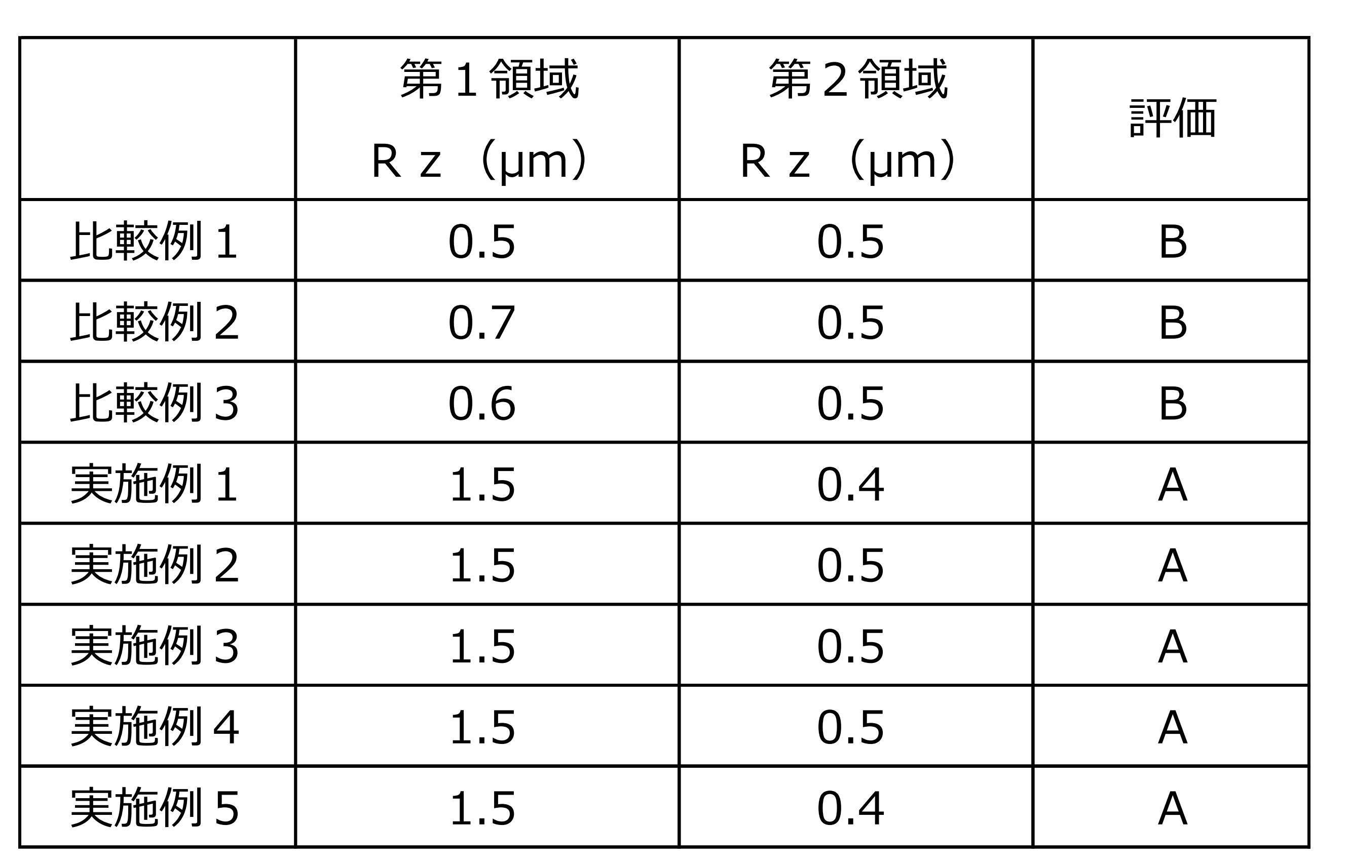
表2に示されるように、第1塗膜領域への電離放射線の積算照射量を適切に設定することにより、突出点群が適切に形成され、その後の加熱によっても突出点群が維持されることが確認された。また、第2塗膜領域に形成された第1物質の析出体を加熱により適切に溶解することによって、第2塗膜領域から形成された第2領域を平滑な面とすることができることも確認された。すなわち、本発明の一実施形態に係る製造方法を実施することにより、反射防止機能を有する領域と反射性の高い領域とを有する外観層を製造することができることが確認された。
(実施例6から実施例13)
実施例1で用いた第1物質25gを第1溶媒50mLに溶解して第1溶液を得て、第2物質25gを第2溶媒50mLに溶解して第2溶液を得た。第1溶液50mLと第2溶液50mLとを混合して、さらに重合開始剤としてケトン系重合開始剤(BASF社製「Irgacure 184」)を固形分に対して2質量%添加して、混合溶液を得た。
この混合溶液に、第1物質の質量および第2物質の質量の総和を基準とした表3に示される添加量(単位:質量%)で、第3物質を添加した。各実施例に係る第3物質の物質名および融点は表3に示したとおりである。第3物質はいずれも水酸基を有し、水酸基を有する点で第1物質と共通するため、第3物質は第1物質に相溶性を有する。それゆえ、第3物質が添加された液状体を用いて形成される析出体は、第1物質および第3物質を含む。#12バーコーターを用いて塗布直後の塗膜の厚さを14μmとしたこと以外は、実施例1と同様にして、第1領域および第2領域を有する外観層を基材上に形成した。
実施例1で用いた第1物質25gを第1溶媒50mLに溶解して第1溶液を得て、第2物質25gを第2溶媒50mLに溶解して第2溶液を得た。第1溶液50mLと第2溶液50mLとを混合して、さらに重合開始剤としてケトン系重合開始剤(BASF社製「Irgacure 184」)を固形分に対して2質量%添加して、混合溶液を得た。
この混合溶液に、第1物質の質量および第2物質の質量の総和を基準とした表3に示される添加量(単位:質量%)で、第3物質を添加した。各実施例に係る第3物質の物質名および融点は表3に示したとおりである。第3物質はいずれも水酸基を有し、水酸基を有する点で第1物質と共通するため、第3物質は第1物質に相溶性を有する。それゆえ、第3物質が添加された液状体を用いて形成される析出体は、第1物質および第3物質を含む。#12バーコーターを用いて塗布直後の塗膜の厚さを14μmとしたこと以外は、実施例1と同様にして、第1領域および第2領域を有する外観層を基材上に形成した。
得られた外観層の第1領域および第2領域について、次の評価を行った。
(1)JIS B0601:2001において規定される表面粗さの最大高さRz(単位:μm)
(2)JIS K7375:2008において規定される全光線透過率(単位:%)
(3)JIS K7136:2000において規定されるヘーズ(ヘイズ、単位:%)
第2領域については、ギラツキの程度についてさらに評価した。
(4)ギラツキ
一般的な外観検査用の蛍光灯が照射された外観層を目視して、次の3水準で評価した。
(A)ギラツキなし
(B)軽度のギラツキあり
(C)明確なギラツキあり
評価結果を表4に示す。
(1)JIS B0601:2001において規定される表面粗さの最大高さRz(単位:μm)
(2)JIS K7375:2008において規定される全光線透過率(単位:%)
(3)JIS K7136:2000において規定されるヘーズ(ヘイズ、単位:%)
第2領域については、ギラツキの程度についてさらに評価した。
(4)ギラツキ
一般的な外観検査用の蛍光灯が照射された外観層を目視して、次の3水準で評価した。
(A)ギラツキなし
(B)軽度のギラツキあり
(C)明確なギラツキあり
評価結果を表4に示す。

表4に示されるように、第3物質を添加した場合(実施例6から実施例12)には、第3物質を添加しない場合(実施例13)に比べて、第2領域の最大高さRzが小さくなり、面平滑性が向上した。また、第3物質を添加することにより、ヘイズが低減される傾向があることおよびギラツキが生じにくくなる傾向があることが確認された。この傾向は、添加した第3物質の融点が低く、第3物質の添加量が多いほど顕著であった。なお、第1領域および第2領域のいずれについても、第3物質を添加したことによる透過率の変化はほとんど認められなかった。第1領域において、第3物質を添加したことにより最大高さRzおよびヘイズが低減する傾向がみられたが、その程度は、いずれも第3物質を添加しない場合(実施例13)に対する変化率で10%以下であった。
100 光学パネル
10 基材
20 外観層
R1 第1領域
R2 第2領域
R1A 第1領域R1の面(第1領域面)
R2A 第2領域R2の面(第2領域面)
21 突出点群
22 上層部分
23 下層部分
24 混合樹脂系材料からなる層
S101 第1ステップ
S102 第2ステップ
S103 第3ステップ
S104 第4ステップ
S105 第5ステップ
30 塗膜
31 混合溶媒
41 第1物質
42 第2物質
32 第1溶媒
33 第2溶媒
34 析出塗膜
41c 析出体
LRD 光源
UVL 電離放射線(紫外光)
MSK マスク
HD 加熱装置
R11 第1塗膜領域
R12 第2塗膜領域
10 基材
20 外観層
R1 第1領域
R2 第2領域
R1A 第1領域R1の面(第1領域面)
R2A 第2領域R2の面(第2領域面)
21 突出点群
22 上層部分
23 下層部分
24 混合樹脂系材料からなる層
S101 第1ステップ
S102 第2ステップ
S103 第3ステップ
S104 第4ステップ
S105 第5ステップ
30 塗膜
31 混合溶媒
41 第1物質
42 第2物質
32 第1溶媒
33 第2溶媒
34 析出塗膜
41c 析出体
LRD 光源
UVL 電離放射線(紫外光)
MSK マスク
HD 加熱装置
R11 第1塗膜領域
R12 第2塗膜領域
Claims (29)
- 透光性を備えた基材と、前記基材の上に位置する外観層とを備える光学パネルであって、
前記外観層は、前記光学パネルの前記外観層側からの入射光の反射率が相対的に低い第1領域および前記反射率が相対的に高い第2領域を備え、
前記外観層は、第1樹脂系材料および第2樹脂系材料を含み、
前記第1領域の面は、前記第1樹脂系材料からなり前記外観層の厚さ方向に突出して外光を散乱する突出点群を備えること
を特徴とする光学パネル。 - 前記第1領域は前記外観層の厚さ方向に組成が相違し、前記基材に対向する側とは反対側における前記第1樹脂系材料の含有量の前記第2樹脂系材料の含有量に対する比は、前記基材に対向する側における前記第1樹脂系材料の含有量の前記第2樹脂系材料の含有量に対する比よりも高い、請求項1に記載の光学パネル。
- 前記突出点群は、前記第2領域の面よりも突出している、請求項1または2に記載の光学パネル。
- 前記第1領域と前記第2領域とは、全体組成が等しく、前記外観層の厚さ方向の組成分布が相違する、請求項1から3のいずれか一項に記載の光学パネル。
- 透光性を備えた基材と、前記基材の上に位置する外観層とを備える光学パネルであって、
前記外観層は、第1樹脂系材料および第2樹脂系材料を含み、
前記外観層の面は、少なくとも一部の領域において、前記第1樹脂系材料からなり前記外観層の厚さ方向に突出して外光を散乱する突出点群を備えること
を特徴とする光学パネル。 - 前記突出点群を備える領域は前記外観層の厚さ方向に組成が相違し、前記基材に対向する側とは反対側における前記第1樹脂系材料の含有量の前記第2樹脂系材料の含有量に対する比は、前記基材に対向する側における前記第1樹脂系材料の含有量の前記第2樹脂系材料の含有量に対する比よりも高い、請求項5に記載の光学パネル。
- 前記外観層はフィラー成分をさらに含む、請求項1から6のいずれか一項に記載の光学パネル。
- 前記外観層はフィラー成分を含まない、請求項1から6のいずれか一項に記載の光学パネル。
- 前記第1樹脂系材料は電離放射線重合性の第1物質の重合体を含み、前記第2樹脂系材料は、前記第1物質とは異なる電離放射線重合性の第2物質の重合体を含む、請求項1から8のいずれか一項に記載の光学パネル。
- 前記外観層は重合開始剤を含む、請求項9に記載の光学パネル。
- 前記外観層は前記第1物質に対する相溶性を有する第3物質を含む、請求項9または10に記載の光学パネル。
- 前記第3物質がフェノール系化合物である、請求項11に記載の光学パネル。
- 透光性を有する基材と、前記基材の上に位置して外光を散乱する突出点群を備える面を有する外観層とを備える光学パネルの製造方法であって、
電離放射線重合性の第1物質と、前記第1物質とは異なる電離放射線重合性の第2物質と、前記第2物質よりも前記第1物質を溶解しやすい第1溶媒と、前記第1物質よりも前記第2物質を溶解しやすく前記第1溶媒よりも沸点が高い第2溶媒と、を含有する液状体を、前記基材の一方の面に塗布して前記基材上に塗膜を形成する第1ステップ;
前記塗膜に含有される前記第1溶媒を揮発させることにより、前記第1物質を含む析出体を前記塗膜の表面に位置させて析出塗膜を得る第2ステップ;および
前記析出塗膜の少なくとも一部の領域に電離放射線を照射することにより、前記電離放射線が照射された領域に位置する前記第1物質および前記第2物質を重合させる第3ステップ
を備え、
前記第3ステップにより、前記外観層の前記突出点群を備える面が形成されることを特徴とする光学パネルの製造方法。 - 前記第3ステップでは、前記析出塗膜の全体に前記電離放射線を照射することにより、前記突出点群を全面に備える前記外観層を前記析出塗膜から形成する、請求項13に記載の光学パネルの製造方法。
- 前記外観層は、前記突出点群を備える面を有する第1領域と、前記突出点群を備えない面を有する第2領域とからなり、
前記第3ステップでは、前記析出塗膜の一部の領域である第1塗膜領域について前記電離放射線を照射することにより、前記第1塗膜領域に位置する前記第1物質および前記第2物質を重合させて、前記第1領域を形成し、
前記第3ステップに続いて、
前記析出塗膜における前記電離放射線が照射されていない第2塗膜領域を加熱して、前記第2塗膜領域の面平滑性を高める第4ステップ;および
前記面平滑性が高められた第2塗膜領域に電離放射線を照射することにより、前記第2塗膜領域に位置する前記第1物質および前記第2物質を重合させて、前記第2領域を形成する第5ステップ
を備える、請求項13に記載の光学パネルの製造方法。 - 前記液状体はフィラー成分をさらに含む、請求項13から15のいずれか一項に記載の光学パネルの製造方法。
- 前記液状体はフィラー成分を含まない、請求項13から15のいずれか一項に記載の光学パネルの製造方法。
- 前記液状体は重合開始剤を含み、前記第1物質および前記第2物質の重合は、電磁波の照射により行う、請求項13から17のいずれか一項に記載の光学パネルの製造方法。
- 前記第4ステップでは、前記析出塗膜における前記第1物質を含む析出体が溶融するように加熱を行う、請求項15から18のいずれか一項に記載の光学パネルの製造方法。
- 前記液状体は前記第1物質に対する相溶性を有する第3物質を含有し、前記第2ステップで形成される前記第1物質を含む析出体は前記第3物質を含み、前記第1物質を含む析出体は前記第1物質からなる析出体よりも融点が低い、請求項19に記載の光学パネルの製造方法。
- 前記第3物質がフェノール系化合物である、光学パネルの製造方法。
- 請求項1から12のいずれか一項に記載される光学パネルを備える機器。
- 転写元面を有する転写層を備える転写体であって、
前記転写層は、電離放射線重合性の第1物質の重合体を含む第1樹脂系材料、および前記第1物質とは異なる電離放射線重合性の第2物質の重合体を含む第2樹脂系材料を含み、
前記転写元面は、前記第1樹脂系材料からなり前記転写層の厚さ方向に突出して外光を散乱する突出点群を備え、
前記転写層における前記転写元面を含む領域は、前記転写層の厚さ方向に組成が相違し、前記転写元面側における前記第1樹脂系材料の含有量の前記第2樹脂系材料の含有量に対する比は、前記転写元面側とは反対側における前記第1樹脂系材料の含有量の前記第2樹脂系材料の含有量に対する比よりも高いこと
を特徴とする転写体。 - 前記第1物質に対する相溶性を有する第3物質を含む、請求項23に記載の転写体。
- 前記第3物質がフェノール系化合物である、請求項23または24に記載の転写体。
- 外光を散乱する突出点群を備える転写元面を有する転写層を備える転写体の製造方法であって、
電離放射線重合性の第1物質と、前記第1物質とは異なる電離放射線重合性の第2物質と、前記第2物質よりも前記第1物質を溶解しやすい第1溶媒と、前記第1物質よりも前記第2物質を溶解しやすく前記第1溶媒よりも沸点が高い第2溶媒と、を含有する液状体を、基材の一方の面に塗布して前記基材上に塗膜を形成する第1ステップ;
前記塗膜に含有される前記第1溶媒を揮発させることにより、前記第1物質を含む析出体を前記塗膜の表面に位置させて析出塗膜を得る第2ステップ;および
前記析出塗膜の少なくとも一部の領域に電離放射線を照射することにより、前記電離放射線が照射された領域に位置する前記第1物質および前記第2物質を重合させる第3ステップ
を備え、
前記第3ステップにより、前記突出点群を備える前記転写元面が形成されることを特徴とする転写体の製造方法。 - 前記転写層は、前記突出点群を備える面を有する第1領域と、前記突出点群を備えない面を有する第2領域とからなり、
前記第3ステップでは、前記析出塗膜の一部の領域である第1塗膜領域について前記電離放射線を照射することにより、前記第1塗膜領域に位置する前記第1物質および前記第2物質を重合させて、前記第1領域を形成し、
前記第3ステップに続いて、
前記析出塗膜における前記電離放射線が照射されていない第2塗膜領域を加熱して、前記第2塗膜領域の面平滑性を高める第4ステップ;および
前記面平滑性が高められた第2塗膜領域に電離放射線を照射することにより、前記第2塗膜領域に位置する前記第1物質および前記第2物質を重合させて、前記第2領域を形成する第5ステップ
を備える、請求項26に記載の転写体の製造方法。 - 前記第4ステップでは、前記析出塗膜における前記第1物質を含む析出体が溶融するように加熱を行い、
前記液状体は前記第1物質に対する相溶性を有する第3物質を含有し、前記第2ステップで形成される前記第1物質を含む析出体は前記第3物質を含み、前記第1物質を含む析出体は前記第1物質からなる析出体よりも融点が低い、請求項27に記載の転写体の製造方法。 - 前記第3物質がフェノール系化合物である、請求項27または28に記載の転写体の製造方法。
Priority Applications (2)
| Application Number | Priority Date | Filing Date | Title |
|---|---|---|---|
| CN201780076597.XA CN110073250A (zh) | 2016-11-01 | 2017-10-25 | 光学面板及其制造方法、以及设备 |
| JP2018548959A JP6924202B2 (ja) | 2016-11-01 | 2017-10-25 | 光学パネルおよびその製造方法、機器ならびに転写体およびその製造方法 |
Applications Claiming Priority (4)
| Application Number | Priority Date | Filing Date | Title |
|---|---|---|---|
| JP2016-214240 | 2016-11-01 | ||
| JP2016214240 | 2016-11-01 | ||
| JP2017108950 | 2017-06-01 | ||
| JP2017-108950 | 2017-06-01 |
Publications (1)
| Publication Number | Publication Date |
|---|---|
| WO2018084052A1 true WO2018084052A1 (ja) | 2018-05-11 |
Family
ID=62076169
Family Applications (1)
| Application Number | Title | Priority Date | Filing Date |
|---|---|---|---|
| PCT/JP2017/038542 Ceased WO2018084052A1 (ja) | 2016-11-01 | 2017-10-25 | 光学パネルおよびその製造方法ならびに機器 |
Country Status (3)
| Country | Link |
|---|---|
| JP (1) | JP6924202B2 (ja) |
| CN (1) | CN110073250A (ja) |
| WO (1) | WO2018084052A1 (ja) |
Citations (3)
| Publication number | Priority date | Publication date | Assignee | Title |
|---|---|---|---|---|
| JP2008046497A (ja) * | 2006-08-18 | 2008-02-28 | Dainippon Printing Co Ltd | 光学積層体、その製造方法、偏光板及び画像表示装置 |
| JP2008216330A (ja) * | 2007-02-28 | 2008-09-18 | Lintec Corp | 防眩性ハードコートフィルム |
| WO2013191091A1 (ja) * | 2012-06-22 | 2013-12-27 | シャープ株式会社 | 反射防止構造体、転写用型、これらの製造方法、及び、表示装置 |
Family Cites Families (21)
| Publication number | Priority date | Publication date | Assignee | Title |
|---|---|---|---|---|
| JPH1164611A (ja) * | 1997-08-26 | 1999-03-05 | Nitto Denko Corp | 光拡散フィルム |
| AU7064400A (en) * | 1999-09-20 | 2001-04-24 | 3M Innovative Properties Company | Optical films having at least one particle-containing layer |
| JP2002148405A (ja) * | 2000-11-07 | 2002-05-22 | Nitto Denko Corp | 反射防止フィルムおよびそれを用いた低反射偏光板 |
| JP4120196B2 (ja) * | 2001-10-19 | 2008-07-16 | コニカミノルタホールディングス株式会社 | 防眩性低反射フィルム、前記フィルムの製造方法、偏光板及び表示装置 |
| AU2003208610A1 (en) * | 2002-02-25 | 2003-09-09 | Fuji Photo Film Co., Ltd. | Antiglare and antireflection film, polarizing plate and display device |
| CN1503009A (zh) * | 2002-11-20 | 2004-06-09 | 力特光电科技股份有限公司 | 抗眩膜 |
| CN100353187C (zh) * | 2004-03-29 | 2007-12-05 | 株式会社巴川制纸所 | 防眩薄膜 |
| JP2007182519A (ja) * | 2006-01-10 | 2007-07-19 | Nippon Paint Co Ltd | アンチブロッキング性光硬化性樹脂組成物、それを基材上に被覆硬化したアンチブロッキング性構造体およびその製法 |
| JP2008051944A (ja) * | 2006-08-23 | 2008-03-06 | Sharp Corp | 防眩性フィルム及び表示装置 |
| JPWO2009001911A1 (ja) * | 2007-06-28 | 2010-08-26 | ソニー株式会社 | 光学フィルムおよびその製造方法、並びにそれを用いた防眩性偏光子および表示装置 |
| JP5163943B2 (ja) * | 2008-02-26 | 2013-03-13 | 住友化学株式会社 | 防眩フィルム、防眩性偏光板および画像表示装置 |
| JP2010163535A (ja) * | 2009-01-15 | 2010-07-29 | Nippon Paint Co Ltd | アンチブロッキング性硬化性樹脂組成物、アンチブロッキング性ハードコートフィルム、アンチブロッキング性層状構造体、アンチブロッキング性層状構造体を含む表示装置およびそれらの製造方法 |
| CN102483475B (zh) * | 2009-09-04 | 2014-05-21 | 住友化学株式会社 | 光扩散膜及其制造方法、光扩散性偏振板以及液晶显示装置 |
| JP5779863B2 (ja) * | 2009-11-30 | 2015-09-16 | 大日本印刷株式会社 | 光学フィルムの製造方法、光学フィルム、偏光板及びディスプレイ |
| CN102884453B (zh) * | 2010-05-07 | 2015-04-01 | 3M创新有限公司 | 包括微结构化表面的抗反射膜 |
| US20120013987A1 (en) * | 2010-07-16 | 2012-01-19 | Kazuhiro Oki | Light scattering sheet and method for producing the same |
| JP5277273B2 (ja) * | 2011-03-14 | 2013-08-28 | 富士フイルム株式会社 | 光学フィルムの製造方法 |
| JP2013190628A (ja) * | 2012-03-14 | 2013-09-26 | Toppan Printing Co Ltd | 反射防止体 |
| JP6190581B2 (ja) * | 2012-10-19 | 2017-08-30 | 株式会社ダイセル | 防眩フィルム及びその製造方法 |
| JP6167005B2 (ja) * | 2013-10-04 | 2017-07-19 | 富士フイルム株式会社 | 反射防止フィルム、偏光板、カバーガラス、及び画像表示装置 |
| JP6186294B2 (ja) * | 2014-03-07 | 2017-08-23 | 富士フイルム株式会社 | 反射防止フィルム、偏光板、画像表示装置、及び反射防止フィルムの製造方法 |
-
2017
- 2017-10-25 WO PCT/JP2017/038542 patent/WO2018084052A1/ja not_active Ceased
- 2017-10-25 JP JP2018548959A patent/JP6924202B2/ja active Active
- 2017-10-25 CN CN201780076597.XA patent/CN110073250A/zh active Pending
Patent Citations (3)
| Publication number | Priority date | Publication date | Assignee | Title |
|---|---|---|---|---|
| JP2008046497A (ja) * | 2006-08-18 | 2008-02-28 | Dainippon Printing Co Ltd | 光学積層体、その製造方法、偏光板及び画像表示装置 |
| JP2008216330A (ja) * | 2007-02-28 | 2008-09-18 | Lintec Corp | 防眩性ハードコートフィルム |
| WO2013191091A1 (ja) * | 2012-06-22 | 2013-12-27 | シャープ株式会社 | 反射防止構造体、転写用型、これらの製造方法、及び、表示装置 |
Also Published As
| Publication number | Publication date |
|---|---|
| JPWO2018084052A1 (ja) | 2019-06-27 |
| JP6924202B2 (ja) | 2021-08-25 |
| CN110073250A (zh) | 2019-07-30 |
Similar Documents
| Publication | Publication Date | Title |
|---|---|---|
| KR100932825B1 (ko) | 눈부심-방지 필름의 제조 방법, 눈부심-방지 필름, 눈부심-방지 편광자, 표시 장치 및 광학 필름 | |
| KR101781206B1 (ko) | 마이크로 렌즈 광학시트, 및 이를 이용한 백라이트 유닛 및 액정 표시 장치 | |
| WO1995031737A1 (en) | Glare-proof film | |
| JP2008233870A (ja) | 防眩性フィルムおよびその製造方法、ならびに表示装置 | |
| TW201718241A (zh) | 包括微結構化各向異性漫射器之絕緣玻璃單元和微光學層及方法 | |
| TWI332103B (en) | Light-diffusing film | |
| JP2017181772A (ja) | 貼付型プロジェクションスクリーン | |
| WO2005083510A1 (ja) | 光拡散性スクリーン | |
| WO2019208136A1 (ja) | 遮光フィルム及び遮光フィルムの製造方法 | |
| JP2023513542A (ja) | 光学フィルムおよびこれを含むマイクロledディスプレイ | |
| JP6681726B2 (ja) | 透明導電性フィルム | |
| TWI317444B (en) | Optical film having high hardness and use thereof | |
| TWI374315B (ja) | ||
| JP6924202B2 (ja) | 光学パネルおよびその製造方法、機器ならびに転写体およびその製造方法 | |
| TWI865442B (zh) | 防眩薄膜 | |
| JP2008152268A (ja) | 防眩フィルムおよびその製造方法 | |
| WO2019208135A1 (ja) | 遮光フィルム及び遮光フィルムの製造方法 | |
| CN100353187C (zh) | 防眩薄膜 | |
| JP4815789B2 (ja) | 拡散レンズアレイシート、透過型スクリーン及び背面投射型ディスプレイ装置 | |
| JP2010002466A (ja) | 光拡散板、バックライトユニットおよびディスプレイ装置 | |
| CN106154371A (zh) | 复合式反射片及其制作方法 | |
| JP2004077781A (ja) | 拡散フィルム | |
| JP2005037802A (ja) | 光散乱フィルムおよびそれを用いた表示装置 | |
| JP4372338B2 (ja) | 光拡散層、光拡散性シート及び光学素子 | |
| JP2006293193A (ja) | フィルムレンチキュラーレンズ用支持板 |
Legal Events
| Date | Code | Title | Description |
|---|---|---|---|
| 121 | Ep: the epo has been informed by wipo that ep was designated in this application |
Ref document number: 17867429 Country of ref document: EP Kind code of ref document: A1 |
|
| ENP | Entry into the national phase |
Ref document number: 2018548959 Country of ref document: JP Kind code of ref document: A |
|
| NENP | Non-entry into the national phase |
Ref country code: DE |
|
| 122 | Ep: pct application non-entry in european phase |
Ref document number: 17867429 Country of ref document: EP Kind code of ref document: A1 |