WO2018074255A1 - 接続端子および接続端子の製造方法 - Google Patents
接続端子および接続端子の製造方法 Download PDFInfo
- Publication number
- WO2018074255A1 WO2018074255A1 PCT/JP2017/036405 JP2017036405W WO2018074255A1 WO 2018074255 A1 WO2018074255 A1 WO 2018074255A1 JP 2017036405 W JP2017036405 W JP 2017036405W WO 2018074255 A1 WO2018074255 A1 WO 2018074255A1
- Authority
- WO
- WIPO (PCT)
- Prior art keywords
- tin
- alloy
- palladium
- connection terminal
- layer
- Prior art date
- Legal status (The legal status is an assumption and is not a legal conclusion. Google has not performed a legal analysis and makes no representation as to the accuracy of the status listed.)
- Ceased
Links
Images


Classifications
-
- H—ELECTRICITY
- H01—ELECTRIC ELEMENTS
- H01B—CABLES; CONDUCTORS; INSULATORS; SELECTION OF MATERIALS FOR THEIR CONDUCTIVE, INSULATING OR DIELECTRIC PROPERTIES
- H01B1/00—Conductors or conductive bodies characterised by the conductive materials; Selection of materials as conductors
- H01B1/02—Conductors or conductive bodies characterised by the conductive materials; Selection of materials as conductors mainly consisting of metals or alloys
-
- C—CHEMISTRY; METALLURGY
- C23—COATING METALLIC MATERIAL; COATING MATERIAL WITH METALLIC MATERIAL; CHEMICAL SURFACE TREATMENT; DIFFUSION TREATMENT OF METALLIC MATERIAL; COATING BY VACUUM EVAPORATION, BY SPUTTERING, BY ION IMPLANTATION OR BY CHEMICAL VAPOUR DEPOSITION, IN GENERAL; INHIBITING CORROSION OF METALLIC MATERIAL OR INCRUSTATION IN GENERAL
- C23F—NON-MECHANICAL REMOVAL OF METALLIC MATERIAL FROM SURFACE; INHIBITING CORROSION OF METALLIC MATERIAL OR INCRUSTATION IN GENERAL; MULTI-STEP PROCESSES FOR SURFACE TREATMENT OF METALLIC MATERIAL INVOLVING AT LEAST ONE PROCESS PROVIDED FOR IN CLASS C23 AND AT LEAST ONE PROCESS COVERED BY SUBCLASS C21D OR C22F OR CLASS C25
- C23F1/00—Etching metallic material by chemical means
-
- C—CHEMISTRY; METALLURGY
- C23—COATING METALLIC MATERIAL; COATING MATERIAL WITH METALLIC MATERIAL; CHEMICAL SURFACE TREATMENT; DIFFUSION TREATMENT OF METALLIC MATERIAL; COATING BY VACUUM EVAPORATION, BY SPUTTERING, BY ION IMPLANTATION OR BY CHEMICAL VAPOUR DEPOSITION, IN GENERAL; INHIBITING CORROSION OF METALLIC MATERIAL OR INCRUSTATION IN GENERAL
- C23F—NON-MECHANICAL REMOVAL OF METALLIC MATERIAL FROM SURFACE; INHIBITING CORROSION OF METALLIC MATERIAL OR INCRUSTATION IN GENERAL; MULTI-STEP PROCESSES FOR SURFACE TREATMENT OF METALLIC MATERIAL INVOLVING AT LEAST ONE PROCESS PROVIDED FOR IN CLASS C23 AND AT LEAST ONE PROCESS COVERED BY SUBCLASS C21D OR C22F OR CLASS C25
- C23F1/00—Etching metallic material by chemical means
- C23F1/10—Etching compositions
- C23F1/14—Aqueous compositions
- C23F1/32—Alkaline compositions
- C23F1/40—Alkaline compositions for etching other metallic material
-
- C—CHEMISTRY; METALLURGY
- C23—COATING METALLIC MATERIAL; COATING MATERIAL WITH METALLIC MATERIAL; CHEMICAL SURFACE TREATMENT; DIFFUSION TREATMENT OF METALLIC MATERIAL; COATING BY VACUUM EVAPORATION, BY SPUTTERING, BY ION IMPLANTATION OR BY CHEMICAL VAPOUR DEPOSITION, IN GENERAL; INHIBITING CORROSION OF METALLIC MATERIAL OR INCRUSTATION IN GENERAL
- C23F—NON-MECHANICAL REMOVAL OF METALLIC MATERIAL FROM SURFACE; INHIBITING CORROSION OF METALLIC MATERIAL OR INCRUSTATION IN GENERAL; MULTI-STEP PROCESSES FOR SURFACE TREATMENT OF METALLIC MATERIAL INVOLVING AT LEAST ONE PROCESS PROVIDED FOR IN CLASS C23 AND AT LEAST ONE PROCESS COVERED BY SUBCLASS C21D OR C22F OR CLASS C25
- C23F1/00—Etching metallic material by chemical means
- C23F1/44—Compositions for etching metallic material from a metallic material substrate of different composition
-
- C—CHEMISTRY; METALLURGY
- C25—ELECTROLYTIC OR ELECTROPHORETIC PROCESSES; APPARATUS THEREFOR
- C25D—PROCESSES FOR THE ELECTROLYTIC OR ELECTROPHORETIC PRODUCTION OF COATINGS; ELECTROFORMING; APPARATUS THEREFOR
- C25D3/00—Electroplating: Baths therefor
- C25D3/02—Electroplating: Baths therefor from solutions
- C25D3/30—Electroplating: Baths therefor from solutions of tin
-
- C—CHEMISTRY; METALLURGY
- C25—ELECTROLYTIC OR ELECTROPHORETIC PROCESSES; APPARATUS THEREFOR
- C25D—PROCESSES FOR THE ELECTROLYTIC OR ELECTROPHORETIC PRODUCTION OF COATINGS; ELECTROFORMING; APPARATUS THEREFOR
- C25D3/00—Electroplating: Baths therefor
- C25D3/02—Electroplating: Baths therefor from solutions
- C25D3/50—Electroplating: Baths therefor from solutions of platinum group metals
-
- C—CHEMISTRY; METALLURGY
- C25—ELECTROLYTIC OR ELECTROPHORETIC PROCESSES; APPARATUS THEREFOR
- C25D—PROCESSES FOR THE ELECTROLYTIC OR ELECTROPHORETIC PRODUCTION OF COATINGS; ELECTROFORMING; APPARATUS THEREFOR
- C25D5/00—Electroplating characterised by the process; Pretreatment or after-treatment of workpieces
- C25D5/10—Electroplating with more than one layer of the same or of different metals
-
- C—CHEMISTRY; METALLURGY
- C25—ELECTROLYTIC OR ELECTROPHORETIC PROCESSES; APPARATUS THEREFOR
- C25D—PROCESSES FOR THE ELECTROLYTIC OR ELECTROPHORETIC PRODUCTION OF COATINGS; ELECTROFORMING; APPARATUS THEREFOR
- C25D5/00—Electroplating characterised by the process; Pretreatment or after-treatment of workpieces
- C25D5/10—Electroplating with more than one layer of the same or of different metals
- C25D5/12—Electroplating with more than one layer of the same or of different metals at least one layer being of nickel or chromium
-
- C—CHEMISTRY; METALLURGY
- C25—ELECTROLYTIC OR ELECTROPHORETIC PROCESSES; APPARATUS THEREFOR
- C25D—PROCESSES FOR THE ELECTROLYTIC OR ELECTROPHORETIC PRODUCTION OF COATINGS; ELECTROFORMING; APPARATUS THEREFOR
- C25D5/00—Electroplating characterised by the process; Pretreatment or after-treatment of workpieces
- C25D5/48—After-treatment of electroplated surfaces
-
- C—CHEMISTRY; METALLURGY
- C25—ELECTROLYTIC OR ELECTROPHORETIC PROCESSES; APPARATUS THEREFOR
- C25D—PROCESSES FOR THE ELECTROLYTIC OR ELECTROPHORETIC PRODUCTION OF COATINGS; ELECTROFORMING; APPARATUS THEREFOR
- C25D5/00—Electroplating characterised by the process; Pretreatment or after-treatment of workpieces
- C25D5/48—After-treatment of electroplated surfaces
- C25D5/50—After-treatment of electroplated surfaces by heat-treatment
- C25D5/505—After-treatment of electroplated surfaces by heat-treatment of electroplated tin coatings, e.g. by melting
-
- C—CHEMISTRY; METALLURGY
- C25—ELECTROLYTIC OR ELECTROPHORETIC PROCESSES; APPARATUS THEREFOR
- C25D—PROCESSES FOR THE ELECTROLYTIC OR ELECTROPHORETIC PRODUCTION OF COATINGS; ELECTROFORMING; APPARATUS THEREFOR
- C25D5/00—Electroplating characterised by the process; Pretreatment or after-treatment of workpieces
- C25D5/60—Electroplating characterised by the structure or texture of the layers
- C25D5/605—Surface topography of the layers, e.g. rough, dendritic or nodular layers
- C25D5/611—Smooth layers
-
- C—CHEMISTRY; METALLURGY
- C25—ELECTROLYTIC OR ELECTROPHORETIC PROCESSES; APPARATUS THEREFOR
- C25D—PROCESSES FOR THE ELECTROLYTIC OR ELECTROPHORETIC PRODUCTION OF COATINGS; ELECTROFORMING; APPARATUS THEREFOR
- C25D5/00—Electroplating characterised by the process; Pretreatment or after-treatment of workpieces
- C25D5/627—Electroplating characterised by the visual appearance of the layers, e.g. colour, brightness or mat appearance
-
- C—CHEMISTRY; METALLURGY
- C25—ELECTROLYTIC OR ELECTROPHORETIC PROCESSES; APPARATUS THEREFOR
- C25D—PROCESSES FOR THE ELECTROLYTIC OR ELECTROPHORETIC PRODUCTION OF COATINGS; ELECTROFORMING; APPARATUS THEREFOR
- C25D7/00—Electroplating characterised by the article coated
-
- H—ELECTRICITY
- H01—ELECTRIC ELEMENTS
- H01R—ELECTRICALLY-CONDUCTIVE CONNECTIONS; STRUCTURAL ASSOCIATIONS OF A PLURALITY OF MUTUALLY-INSULATED ELECTRICAL CONNECTING ELEMENTS; COUPLING DEVICES; CURRENT COLLECTORS
- H01R13/00—Details of coupling devices of the kinds covered by groups H01R12/70 or H01R24/00 - H01R33/00
- H01R13/02—Contact members
- H01R13/03—Contact members characterised by the material, e.g. plating, or coating materials
-
- H—ELECTRICITY
- H01—ELECTRIC ELEMENTS
- H01R—ELECTRICALLY-CONDUCTIVE CONNECTIONS; STRUCTURAL ASSOCIATIONS OF A PLURALITY OF MUTUALLY-INSULATED ELECTRICAL CONNECTING ELEMENTS; COUPLING DEVICES; CURRENT COLLECTORS
- H01R43/00—Apparatus or processes specially adapted for manufacturing, assembling, maintaining, or repairing of line connectors or current collectors or for joining electric conductors
- H01R43/16—Apparatus or processes specially adapted for manufacturing, assembling, maintaining, or repairing of line connectors or current collectors or for joining electric conductors for manufacturing contact members, e.g. by punching and by bending
-
- C—CHEMISTRY; METALLURGY
- C25—ELECTROLYTIC OR ELECTROPHORETIC PROCESSES; APPARATUS THEREFOR
- C25D—PROCESSES FOR THE ELECTROLYTIC OR ELECTROPHORETIC PRODUCTION OF COATINGS; ELECTROFORMING; APPARATUS THEREFOR
- C25D3/00—Electroplating: Baths therefor
- C25D3/02—Electroplating: Baths therefor from solutions
- C25D3/12—Electroplating: Baths therefor from solutions of nickel or cobalt
Definitions
- the present invention relates to a connection terminal and a method for manufacturing the connection terminal, and more particularly to a connection terminal with an alloy exposed on the surface and a method for manufacturing such a connection terminal.
- connection terminal a material in which tin plating is applied to the surface of a base material such as copper or a copper alloy has been used.
- a tin plating layer an insulating tin oxide film is formed on the surface.
- the tin oxide film is broken by a weak force, the metal tin is easily exposed, and the surface of the soft metal tin has a good electrical property. Contact is formed.
- Patent Document 1 discloses a terminal in which a nickel plating layer, a copper plating layer, and a tin plating layer are sequentially laminated on the surface of at least a contact portion of a copper alloy base material with a counterpart material.
- the nickel plating layer is provided to suppress diffusion of copper in the base material into the tin plating layer
- the copper plating layer is provided to suppress generation of an intermetallic compound of nickel and tin. Is provided.
- the terminal insertion force is reduced by limiting the thickness of the tin plating layer.
- the problem of the present invention is that the friction coefficient can be reduced and the change with time at high temperature can be kept small while maintaining the connection reliability as compared with the connection terminal in which tin is exposed on the outermost surface of the contact portion. It is in providing a connection terminal and the manufacturing method of such a connection terminal.
- connection terminal according to the present invention is such that at least a contact portion in electrical contact with the counterpart conductive member has alloy particles made of an intermetallic compound containing tin and palladium on the outermost surface of the contact portion.
- the ratio of tin to palladium rather than pure tin or the intermetallic compound in a plane passing through a point that is exposed and distributed on the surface of the base material and the height of the alloy particles from the surface of the base material is the highest.
- the tin part made of a high alloy is not exposed.
- the tin portion does not exist around the alloy particles. Moreover, it is preferable that the surface of the base material is exposed between the alloy particles.
- the base material may have a nickel or nickel alloy layer, and the intermetallic compound may have a composition of (Ni 0.4 Pd 0.6 ) Sn 4 .
- the ratio of the area occupied by the alloy particles may be 30% or more.
- the average thickness of the layer occupied by the alloy particles is preferably 0.1 ⁇ m or more and 5.0 ⁇ m or less.
- the method for producing a connection terminal includes a step of producing a laminated structure in which a palladium layer and a tin layer are laminated in this order on the surface of a base material, and the intermetallic compound containing tin and palladium by heating the laminated structure A step of forming an alloy particle comprising, and removing a tin portion derived from excess tin that did not form the intermetallic compound and made of pure tin or an alloy having a higher ratio of tin to palladium than the intermetallic compound And a process.
- the step of removing the tin portion may be performed by chemically dissolving tin.
- the ratio of palladium to the total amount of tin and palladium in the laminated structure is preferably 2 atomic% or more. Moreover, the ratio of palladium with respect to the total amount of tin and palladium in the laminated structure is preferably less than 20 atomic%.
- connection terminal the intermetallic compound containing tin and palladium constituting the alloy particles exposed on the outermost surface has high hardness, so that digging and adhesion hardly occur at the contact portion, and are low. A coefficient of friction is obtained.
- the tin that increases the friction coefficient is not exposed on the plane passing through the position where the height of the alloy particles is the highest, the terminal insertion force of the connection terminal can be kept low.
- an intermetallic compound containing tin and palladium has high conductivity and is not easily oxidized, so that low contact resistance can be obtained on the surface of the contact portion. As a result, high connection reliability can be achieved.
- the intermetallic compound containing tin and palladium has already formed a stable intermetallic compound, even if it is heated, it hardly changes over time such as alloying with other metals. Tin, which tends to form intermetallic compounds with other metals due to changes over time, is not exposed on the plane that passes through the position where the height of the alloy particles is the highest. Increase in contact resistance is less likely to occur. Therefore, high connection reliability can be maintained in the long term.
- the layer made of nickel or nickel alloy Suppresses the diffusion of metal atoms from a base material made of copper, etc., so that contact resistance on the outermost surface increases due to the effect of such metal atom diffusion even when heated at high temperatures for a long time. Can be suppressed.
- the proportion of the area occupied by the alloy particles in the contact portion is 30% or more, the contact area between the contact portion of the connection terminal and the counterpart conductive member is ensured, and the contact resistance is particularly reduced. be able to.
- the terminal insertion force can be sufficiently suppressed.
- the average thickness of the layer occupied by the alloy particles is 0.1 ⁇ m or more and 5.0 ⁇ m or less, the effect of reducing the friction coefficient and suppressing the change with time by the alloy particles can be fully enjoyed. .
- the alloy particles made of an intermetallic compound containing tin and palladium as described above are exposed on the outermost surface, and the alloy particles pass through the highest point.
- a structure in which the tin portion is not exposed on the plane can be easily formed on the surface of the connection terminal.
- the step of removing the tin portion is performed by chemically dissolving tin, the removal of the tin portion can be achieved simply and in a state where the remaining amount is small. As a result, in the manufactured connection terminal, the effect of reducing the friction coefficient and suppressing the change with time due to the alloy particles is remarkably obtained.
- the ratio of palladium to the total amount of tin and palladium in the laminated structure is 2 atomic% or more, by ensuring the area of the alloy particles exposed on the outermost surface, in the contact portion of the connection terminal to be manufactured, The friction coefficient can be effectively reduced.
- the ratio of palladium to the total amount of tin and palladium in the laminated structure is 20 atomic%, when the laminated structure is heated, it is easy for excess tin and alloy particles to coexist. After the removal, the intermetallic compound exposed on the outermost surface tends to take the form of an aggregate of particles.
- connection terminal and a manufacturing method thereof according to an embodiment of the present invention will be described in detail with reference to the drawings.
- a contact portion such as a counterpart terminal that is in electrical contact with the counterpart conductive member is made of a terminal material 1 having an alloy particle layer 20 described below on the surface.
- a connection terminal made of such a terminal material 1 can be manufactured by the method for manufacturing a connection terminal according to an embodiment of the present invention.
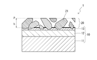
- the terminal material 1 constituting the connection terminal has a layer structure as shown in a schematic cross-sectional view in FIG. That is, the alloy particle layer 20 is formed on the surface of the substrate 10. The alloy particle layer 20 is exposed on the outermost surface of the terminal material 1.
- the base material 10 is mainly composed of a plate-shaped base material 11.
- the base material 11 is made of, for example, copper, aluminum, iron, or an alloy containing them as a main component. Among these, copper or a copper alloy that has high conductivity and is widely used as a base material for connection terminals is particularly suitable.
- the base material 10 can be composed only of the base material 11, but the base material 10 may be appropriately provided with a metal coating layer on the surface of the base material 11.
- a base layer 12 made of nickel or a nickel alloy is formed so as to cover the surface of the base material 11.
- the underlayer 12 plays a role of increasing the adhesion of the alloy particle layer 20 to the base material 11 and suppressing diffusion of metal atoms such as copper from the base material 11 to the alloy particle layer 20.
- Part of the underlayer 12 on the side of the alloy particle layer 20 may become the nickel-tin alloy layer 13 by heating in the process of forming the alloy particle layer 20.
- the nickel-tin alloy layer 13 has a composition of Ni 3 Sn 4 .
- the alloy particle layer 20 is made of an aggregate of alloy particles 21.
- the alloy particles 21 are made of an intermetallic compound containing tin and palladium (tin-palladium alloy).
- the intermetallic compound may be a binary alloy composed only of tin and palladium, or may be a multi-element alloy containing other metals in addition to tin and palladium. In the case of a binary alloy, the intermetallic compound has a composition of PdSn 4 . Examples of metal elements other than tin and palladium constituting the multi-element alloy include metal elements contained in the substrate 10.
- the alloy particles 21 include, in addition to the intermetallic compound, a metal element, an unavoidable impurity, an alloy constituting the substrate 10. A small amount of a palladium phase or the like that is not taken in may be contained.
- each alloy particle 21 is bonded to the base material 10.
- the base layer 12 made of nickel or a nickel alloy is formed on the surface of the base material 10 and a part thereof is the nickel-tin alloy layer 13, a part of the alloy particles 21 on the base material 10 side.
- the region is in a state of being fitted inside the nickel-tin alloy layer 13 and is surrounded by a nickel-tin alloy.
- an outermost surface P that is a virtual plane passing through a point where the height h of the alloy particles 21 from the surface of the base material 10 is highest is assumed.
- the outermost surface P is not exposed with a tin portion made of pure tin or an alloy having a higher tin ratio than in the intermetallic compound constituting the alloy particle 21.
- the tin portion is not exposed on the outermost surface P, it may be present in the voids between the alloy particles 21 in the alloy particle layer 20, but preferably, as shown in FIG. It is better that the tin portion does not exist around the particle 21, that is, at a position in contact with the alloy particle 21. Furthermore, it is desirable that a tin portion does not exist in the alloy particle layer 20, that is, on the surface of the base material 10, except for a tin content that cannot be completely removed in the manufacturing process described later. In addition to the tin portion, it is preferable that no metal other than the tin-palladium alloy constituting the alloy particle 21 exists around the alloy particle 21 except for the metal constituting the base material 10.
- the gap between the alloy particles 21 is formed on the surface of the base material 10, here, as shown by a thick line in the drawing.
- the surface of the nickel-tin alloy layer 13 is exposed.
- the density of the alloy particles 21 is high, the entire surface of the base material 10 is covered with the alloy particles 21 and the surface of the base material 10 may be hardly exposed.
- the size and density of the alloy particles 21 are not particularly limited.
- the average thickness of the alloy particle layer 20 is preferably set to 0.1 ⁇ m or more. Thereby, the characteristics exhibited by the alloy particles 21 such as reduction of a friction coefficient and suppression of change with time, which will be described later, can be fully utilized.
- the average thickness of the alloy particle layer 20 is preferably 5.0 ⁇ m or less. This is because even if the alloy particle layer 20 is formed too thick, the characteristics exhibited by the alloy particles 21 are saturated, and the material cost required for forming the alloy particles 21 increases.
- the average thickness of the alloy particle layer 20 is the amount of the tin-palladium alloy in the form of the alloy particles 21 converted to the thickness of the film that uniformly covers the surface of the substrate 10. Refers to things.
- the terminal material 1 has the alloy particle layer 20 on the surface of the base material 10 in which the alloy particles 21 made of a tin-palladium alloy are exposed on the outermost surface.
- Tin-palladium alloys have high hardness. Therefore, on the surface of the alloy particle layer 20, surface metal digging or adhesion that often occurs on the surface of the tin layer is less likely to occur. Thus, the alloy particles 21 give a lower coefficient of friction than tin on the surface of the terminal material 1.
- the alloy particle layer 20 since the tin portion is not exposed on the outermost surface P, a situation in which the friction coefficient of the alloy particle layer 20 is increased due to the contribution of the tin portion does not occur, and the alloy particle 21 The given low friction coefficient can be used as the friction coefficient of the alloy particle layer 20 as it is. As a result, the alloy particle layer 20 as a whole has a lower friction coefficient on the surface than the surface of the tin layer. Furthermore, in the terminal material 1 described above, part of the alloy particles 21 are fitted into the nickel-tin alloy layer 13 and are firmly bonded to the base material 10, so that the peeling of the alloy particles 21 due to friction is suppressed. This also contributes to the reduction of the friction coefficient.
- the dynamic friction coefficient between the terminal material 1 and the counterpart conductive member can be set to 0.4 or less.
- the insertion force of the connection terminal can be kept low.
- the insertion force increases as the number of connection terminals increases, so that the effect of reducing the insertion force by using the terminal material 1 is greatly enjoyed. Can do.
- Tin-palladium alloys have high conductivity and are not easily oxidized. Therefore, a low contact resistance is obtained on the surface of the alloy particle layer 20. Although the contact resistance is larger than that of the material on which the tin plating layer is formed, the contact resistance can be suppressed sufficiently low as a connection terminal. For example, the contact resistance can be suppressed to 1 m ⁇ or less like the tin plating layer. As described above, since the contact resistance of the surface of the terminal material 1 is kept low, good electrical contact is formed at the contact portion of the connection terminal, and high connection reliability is obtained.
- the contact resistance on the surface of the alloy particle layer 20 decreases as the substantial contact area with the counterpart conductive member increases. Therefore, the larger the exposure amount of the alloy particles 21 on the outermost surface P, the lower the contact resistance.
- the alloy particle layer 20 may be formed so that the ratio of the area occupied by the alloy particles 21 on the surface of the substrate 10 (area ratio) exceeds 15%. More preferably, the area ratio may be 30% or more.
- the area ratio can be evaluated by calculating the ratio of the area occupied by the alloy particles 21 in the entire visual field region in an image obtained by observing the surface of the alloy particle layer 20 with a microscope such as a scanning electron microscope (SEM). .
- the alloy particles 21 have already formed a stable intermetallic compound, and even when heated further, the alloy particles 21 can interact with other metals existing in the periphery, such as the metal constituting the substrate 10. Difficult to cause formation of intermetallic compounds by diffusion. Therefore, even when the terminal material 1 is heated for a long time by the surrounding environment or energization, the alloy particle layer 20 is less likely to change with time due to the formation of intermetallic compounds with other metals. If an intermetallic compound is formed with another metal, the formed intermetallic compound may be oxidized on the outermost surface of the terminal material 1 to increase the contact resistance. However, in the present terminal material 1, such a situation is less likely to occur due to the stability of the tin-palladium alloy, and it is possible to maintain a high connection reliability for a long time.
- the tin portion is exposed on the outermost surface P in the alloy particle layer 20, tin is likely to form an intermetallic compound with a metal such as nickel, so that the terminal material 1 is heated for a long time. At this time, the tin portion may form an intermetallic compound by mutual diffusion between the base layer 12 and the metal constituting the base material 10 such as nickel of the nickel-tin alloy layer 13. If the intermetallic compound is oxidized on the outermost surface of the terminal contact portion, it can lead to an increase in contact resistance. However, in the terminal material 1, since the tin portion is not exposed on the outermost surface P of the alloy particle layer 20, such a situation can be avoided and high connection reliability can be ensured over a long period of time. In particular, not only the outermost surface P but also the surroundings of the alloy particles 21 and the tin part in the alloy particle layer 20 do not substantially exist, so that the deterioration of connection reliability due to heating is avoided to a higher degree. be able to.
- the rate of increase in contact resistance when the terminal material 1 is heated at 160 ° C. can be suppressed to 10% or less, further 5% or less, based on the value before heating.
- Examples of the heating time for evaluating the increase in contact resistance include 120 hours or longer.
- the terminal material 1 demonstrated above can be manufactured by the following methods, for example.
- the base material 10 is prepared.
- the base layer 12 may be formed on the surface of the base material 11 by plating or the like.
- the palladium layer and the tin layer are laminated
- this laminated structure is heated.
- alloying proceeds between the tin layer and the palladium layer, and alloy particles 21 made of an intermetallic compound containing tin and palladium are formed.
- a part of the base layer 12 made of nickel or a nickel alloy forms an intermetallic compound with the tin layer having a laminated structure, thereby forming a nickel-tin alloy layer 13.
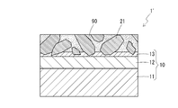
- a precursor 1 'as shown in FIG. 2 is obtained.
- an alloy particle 21 made of an intermetallic compound containing tin and palladium and a layer made of a tin portion 90 are formed on the surface of the base material 10.
- the tin portion 90 is made of pure tin or an alloy having a higher tin ratio than the intermetallic compound constituting the alloy particles 21.
- the tin part 90 is derived from excess tin that did not form an intermetallic compound during heating.
- both the tin portion 90 and the alloy particles 21 are exposed on the outermost surface.
- the alloy particles 21 are exposed on the outermost surface and the tin portion 90 is not exposed on the outermost surface P as shown in FIG. Material 1 can be obtained.
- the removal of the tin part 90 can be easily and effectively performed by chemically dissolving tin.
- tin can be selectively dissolved with almost no change in the alloy particles 21.
- the average thickness of the alloy particle layer 20 and the area ratio of the alloy particles 21 in the manufactured terminal material 1 are selected by selecting the thicknesses of the palladium layer and the tin layer. Can be controlled. At this time, the ratio of palladium to the total amount of tin and palladium (Pd / (Sn + Pd)) is preferably set to 2 atomic% or more. Thereby, through heating, the area ratio of the alloy particles 21 in the SEM image is 30% or more, and it is easy to obtain the terminal material 1 that gives a low contact resistance.
- the proportion of palladium in the laminated structure is preferably less than 20 atomic%.
- the stable composition of the binary alloy between tin and palladium is PdSn 4 , and by setting the ratio of palladium to less than 20 atomic%, heating causes the excess tin portion 90 to be contained. It is easy to take a dispersed state of particulate tin-palladium alloy. By removing the tin portion 90 in this state, the tin-palladium alloy can be easily obtained in the form of an aggregate of alloy particles 21 instead of a smooth layer. In the case where the alloy particles 21 are composed of a multi-element alloy, it is more preferable that the upper limit of the ratio of palladium is determined so that an excessive tin portion 90 remains during heating in consideration of the composition of the multi-element alloy.
- connection terminal structure The connection terminal according to the embodiment of the present invention may be of any type and shape as long as the contact portion that contacts at least the counterpart conductive member is made of the terminal material 1 as described above. .
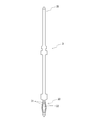
- a press-fit terminal 3 as shown in FIG. 3 can be exemplified.
- the press-fit terminal 3 is an electrical connection terminal having an elongated shape, and has a board connection portion 30 that is press-fitted and connected to a through hole of the board at one end, and is connected to the other connection terminal by fitting or the like at the other end.
- the terminal connection part 35 is provided.
- the terminal connection portion 35 has the shape of a male fitting terminal.
- the substrate connecting portion 30 has a pair of bulging pieces 31 and 31 at a portion to be press-fitted and connected to the through hole.
- the bulging pieces 31, 31 have a shape bulging in a substantially arc shape so as to be separated from each other in a direction orthogonal to the axial direction of the press-fit terminal 3.
- a gap 32 is formed between the pair of bulging pieces 31, 31, and when the press-fit terminal 3 is inserted into the through hole, the pair of bulging pieces 31, 31 are mutually connected. It is compressed so as to be close to each other and elastically deforms. And it recovers elastically and maintains electrical contact with the inner peripheral surface of the through hole.
- a large number of press-fit terminals 3 are held side by side, and can be used as a multipolar board connector.
- the entire press-fit terminal 3 may be formed from the terminal material 1.
- Example 1 An alloy particle exposed sample according to Example 1 was prepared as follows. That is, a nickel base plating layer having a thickness of 1.0 ⁇ m was formed on the surface of a clean copper base material, and a palladium plating layer having a thickness of 0.02 ⁇ m was formed thereon. Subsequently, a tin plating layer having a thickness of 1.0 ⁇ m was formed on the palladium plating layer. By heating this at 300 ° C. in the atmosphere, alloying of the tin plating layer and the palladium plating layer was advanced. Thereafter, the sample was immersed in a mixed aqueous solution of sodium hydroxide and p-nitrophenol to remove excess tin. The surface and the cross section of the obtained sample were observed by SEM, and the state was confirmed.
- the tin plating sample concerning the comparative example 1 was produced as follows. That is, a tin plating layer having a thickness of 1.0 ⁇ m was formed on the surface of the copper base material on which the same nickel base plating layer as described above was formed. And the reflow process was performed by heating at 300 degreeC in air
- Example 1 and Comparative Example 1 were held in the atmosphere at 160 ° C. for 120 hours (hereinafter, this condition may be referred to as “high temperature storage”). After leaving at high temperature, the sample of Example 1 was observed by SEM. For the samples of Example 1 and Comparative Example 1, the load-contact resistance characteristics were measured in the same manner as the measurement for the samples before standing at high temperature after cooling to room temperature.
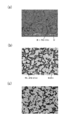
- [Test results] (Evaluation of sample condition) 4A and 4B show surface SEM images of the exposed alloy particle sample of Example 1 before tin removal and after tin removal, respectively.
- alloy particles made of sea-island tin-palladium alloy ((Ni 0.4 Pd 0.6 ) Sn 4 ; the same applies below) as indicated in the figure.
- surroundings is exposed to the surface.
- the structure observed in gray of medium brightness corresponding to the tin portion is not seen around the alloy particles made of the tin-palladium alloy. ing. Instead, a darkly observed nickel-tin alloy layer (Ni 3 Sn 4 ) is seen around the alloy particles.
- FIG. 5 shows an SEM image of the cross section of the sample after removing tin. Also in the cross section, it has been observed that a part of the nickel underlayer is a nickel-tin alloy layer and that alloy particles made of a tin-palladium alloy are exposed on the outermost surface. And the tin part does not exist in the space
- EDX elemental analysis
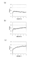
- FIG. 6A shows the load-contact resistance characteristics of the alloy particle-exposed sample after removing tin in Example 1 by a solid line.
- FIG. 6B shows the load-contact resistance characteristics of the tin-plated sample of Comparative Example 1.
- the tin-plated sample shows a lower contact resistance, but the contact resistance of the alloy particle-exposed sample is suppressed to within about twice that of the tin-plated sample.
- Table 2 shows that the contact resistance at a load of 10 N is suppressed to 1.7 times that of the tin-plated sample in the alloy particle exposed sample.
- Such contact resistance of the alloy particle exposed sample is sufficiently low to be used as a connection terminal.
- FIG. 7 shows the results of measurement of the friction coefficient of (a) an alloy particle exposed sample after removing tin (Example 1), (b) an alloy particle exposed sample before removing tin, and (c) a tin plated sample (Comparative Example 2). Indicates. Table 1 shows the maximum value of the friction coefficient. In addition, the reduction amount of the friction coefficient based on the value of the tin plating sample is shown for the alloy particle exposed sample.
- the hard tin-palladium alloy is exposed on the outermost surface, so that the coefficient of friction is lower than that of the tin-plated sample even before the tin is removed. Have. And the friction coefficient is further reduced significantly by removing tin. This is interpreted as a result of the fact that tin, which raises the friction coefficient of the surface by digging or adhesion, is removed from the surface, and only the alloy particles that are hard and give a low friction coefficient are exposed on the outermost surface. Is done.
- FIG. 4C shows an SEM image of the surface of the alloy particle exposed sample from which the tin of Example 1 was removed after being left at a high temperature. Compared with the SEM image before standing at high temperature in FIG. 4B, no significant change is observed in the shape, size, and distribution of the alloy particles. That is, it can be said that the state of the surface has hardly changed even after being left at high temperature.
- Example 1 For the alloy particle exposed sample from which tin was removed in Example 1, the measurement result of load-contact characteristics before standing at high temperature is shown in FIG. Is indicated by a broken line. Both curves almost overlap, and it can be seen that the contact resistance hardly changes even after being left at high temperature.
- Table 2 summarizes the values of contact resistance at a load of 10 N before and after standing at high temperature and the amount of change for the alloy particle exposed sample of Example 1 after tin removal and the tin plated sample of Comparative Example 1.
- the tin plating sample shows an increase rate of 100% or more in contact resistance when left at high temperature. This corresponds to the progress of alloying between tin and the nickel underlayer, and the resulting alloy is oxidized on the outermost surface.
- the resistance increase rate is suppressed to only 2%, as can be seen from the result of FIG. This is because tin that is likely to be alloyed with nickel or the like has been removed from the surface, and only alloy particles made of a tin-palladium alloy that does not easily alloy with other metals even at high temperatures are exposed on the surface. It is interpreted as a result of
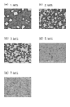
- FIG. 8 the surface SEM image of the alloy particle exposure sample obtained when the ratio of palladium in the laminated structure before a heating is variously changed is shown.
- the palladium content in the laminated structure before heating is shown in the figure.
- FIG. 8 it can be seen that the proportion of alloy particles observed in light gray increases as the proportion of palladium increases.
- the area of the region where the alloy particles coat the sample surface is rapidly increasing.
- Table 3 summarizes the relationship between the proportion of palladium in the laminated structure before heating, the area ratio of the region occupied by the alloy particles obtained by image analysis of the SEM image, and the contact resistance at 10 N (measured only for three samples). .
- the area ratio of the alloy increases as the proportion of palladium before heating increases, and the alloy is in the region where the proportion of palladium is 5.0 atomic% or more. It can be seen that the area ratio of is increasing rapidly. Further, the contact resistance is reduced as the area ratio of the alloy increases with the proportion of palladium before heating. In particular, the contact resistance is drastically reduced in a region where the palladium ratio in which the area ratio of the alloy is 30% or more is 2.0 atomic% or more. The reduction in contact resistance is interpreted as a result of increasing the area ratio of the region occupied by the alloy particles due to an increase in the proportion of palladium, and coming into contact with the counterpart conductive member in a large area.
- the concentration and immersion time of the mixed aqueous solution of sodium hydroxide and p-nitrophenol are adjusted so that the tin part is not completely removed, and a part of the tin part is intentionally left. Good.
Landscapes
- Chemical & Material Sciences (AREA)
- Engineering & Computer Science (AREA)
- Organic Chemistry (AREA)
- Chemical Kinetics & Catalysis (AREA)
- Materials Engineering (AREA)
- Metallurgy (AREA)
- Electrochemistry (AREA)
- General Chemical & Material Sciences (AREA)
- Mechanical Engineering (AREA)
- Manufacturing & Machinery (AREA)
- Electroplating Methods And Accessories (AREA)
- ing And Chemical Polishing (AREA)
- Manufacturing Of Electrical Connectors (AREA)
Abstract
スズを接点部の最表面に露出させた接続端子と比較して、接続信頼性を維持しながら、摩擦係数を低減でき、かつ高温での経時変化を小さく抑えることができる接続端子、およびそのような接続端子の製造方法を提供する。 少なくとも接点部において、スズとパラジウムを含む金属間化合物よりなる合金粒子21が、該接点部の最表面に露出して、基材10の表面に分布しており、合金粒子21の基材10の表面からの高さhが最も高い点を通る平面Pに、純スズまたは金属間化合物よりもパラジウムに対するスズの割合が高い合金よりなるスズ部が露出していない接続端子とする。また、パラジウム層およびスズ層をこの順に積層した積層構造を加熱し、スズとパラジウムを含む金属間化合物よりなる合金粒子21を形成する工程と、金属間化合物を形成しなかった余剰のスズに由来するスズ部を除去する工程と、を有する接続端子の製造方法とする。
Description
本発明は、接続端子および接続端子の製造方法に関し、さらに詳しくは、表面に合金が露出した接続端子、およびそのような接続端子の製造方法に関するものである。
従来一般に、接続端子を構成する材料として、銅または銅合金などの母材の表面にスズめっきが施されたものが用いられていた。スズめっき層においては、表面に絶縁性の酸化スズ被膜が形成されるが、酸化スズ被膜は弱い力で破壊されるため、容易に金属スズが露出し、軟らかい金属スズの表面で、良好な電気的接触が形成される。
例えば、特許文献1において、銅合金製母材の少なくとも相手材との接触部の表面に、順次、ニッケルめっき層、銅めっき層及び錫めっき層を積層してなる端子が開示されている。この端子において、ニッケルめっき層は、母材中の銅が錫めっき層に拡散するのを抑制するために設けられ、銅めっき層は、ニッケルと錫との金属間化合物の生成を抑制するために設けられている。また、錫めっき層の厚みを制限することで、端子挿入力の低減が図られている。
特許文献1に開示される端子のように、スズ層が接点部の最表面に露出されている場合には、スズの軟らかさのために、スズ層の掘り起こしやスズ同士の凝着が起こり、摩擦係数が高くなってしまう。その結果、端子の挿入力が上昇する。特に、多数の端子を備えた多極型のコネクタにおいては、挿入力の上昇の問題が大きくなる。特許文献1に記載されるように、スズ層の厚さを制限することで、摩擦係数をある程度低く抑えることが可能ではあるが、接点部の最表面にスズ層が露出されているかぎり、摩擦係数を大幅に低減することは難しい。
また、スズ層は、加熱を受けた際に、他の金属層との間で、相互拡散によって金属間化合物を形成しやすく、表面状態の経時変化が大きくなる。そのような金属間化合物が接点部の最表面で酸化を受けると、接点部の接触抵抗を上昇させる場合がある。特許文献1に記載されるように、スズ層の下層に設ける金属層の選択により、他の金属のスズ層への拡散およびスズとの金属間化合物の形成を抑制することが可能ではあるが、高温の環境に長時間晒された際には、スズとの金属間化合物の形成が無視できなくなる可能性がある。
本発明の課題は、スズを接点部の最表面に露出させた接続端子と比較して、接続信頼性を維持しながら、摩擦係数を低減でき、かつ高温での経時変化を小さく抑えることができる接続端子、およびそのような接続端子の製造方法を提供することにある。
上記課題を解決するため、本発明にかかる接続端子は、少なくとも相手方導電部材と電気的に接触する接点部において、スズとパラジウムを含む金属間化合物よりなる合金粒子が、該接点部の最表面に露出して、基材の表面に分布しており、前記合金粒子の前記基材の表面からの高さが最も高い点を通る平面に、純スズまたは前記金属間化合物よりもパラジウムに対するスズの割合が高い合金よりなるスズ部が露出していない、というものである。
ここで、前記合金粒子の周囲に、前記スズ部が存在しないとよい。また、前記合金粒子の間に、前記基材の表面が露出しているとよい。
前記基材は、ニッケルまたはニッケル合金の層を有しており、前記金属間化合物が、(Ni0.4Pd0.6)Sn4の組成を有するとよい。
前記接点部において、前記合金粒子が占める面積の割合が、30%以上であるとよい。
前記合金粒子が占める層の平均の厚さが、0.1μm以上、5.0μm以下であるとよい。
本発明にかかる接続端子の製造方法は、基材の表面に、パラジウム層およびスズ層をこの順に積層した積層構造を作製する工程と、前記積層構造を加熱し、スズとパラジウムを含む金属間化合物よりなる合金粒子を形成する工程と、前記金属間化合物を形成しなかった余剰のスズに由来する、純スズまたは前記金属間化合物よりもパラジウムに対するスズの割合が高い合金よりなるスズ部を除去する工程と、を有するものである。
ここで、前記スズ部を除去する工程は、スズを化学的に溶解することによって行うとよい。
前記積層構造におけるスズとパラジウムの合計量に対するパラジウムの割合が、2原子%以上であるとよい。また、前記積層構造におけるスズとパラジウムの合計量に対するパラジウムの割合が、20原子%未満であるとよい。
上記発明にかかる接続端子においては、最表面に露出している合金粒子を構成するスズとパラジウムを含む金属間化合物が高い硬度を有することにより、接点部において、掘り起こしや凝着が起こりにくく、低い摩擦係数が得られる。加えて、合金粒子の高さが最も高い位置を通る平面に、摩擦係数を上昇させるスズが露出していないことにより、接続端子の端子挿入力を低く抑えることができる。
同時に、スズとパラジウムを含む金属間化合物は、高い導電率を有し、また酸化を受けにくいため、接点部の表面において、低い接触抵抗が得られる。その結果、高い接続信頼性を達成することができる。
そして、スズとパラジウムを含む金属間化合物は、既に安定な金属間化合物を形成していることにより、加熱を受けても、他の金属との合金化等、経時的な変化を起こしにくい。経時変化によって他の金属との間に金属間化合物を形成しやすいスズが、合金粒子の高さが最も高い位置を通る平面に露出していないため、接点部の最表面全体として、経時変化による接触抵抗の上昇が起こりにくくなっている。よって、長期的に高い接続信頼性を維持することができる。
ここで、合金粒子の周囲に、スズ部が存在しない場合には、合金粒子の高さが最も高い位置を通る平面内のみならず、合金粒子と接触する部位全体にスズが存在しないので、接点部の表面が、スズの経時変化の影響を受けにくく、接続端子の長期的な接続信頼性を得ることができる。
また、合金粒子の間に、基材の表面が露出している場合には、合金粒子の間の部位にもスズが存在しないことになるので、接続端子の長期的な接続信頼性が一層高まる。
基材が、ニッケルまたはニッケル合金の層を有しており、金属間化合物が、(Ni0.4Pd0.6)Sn4の組成を有する場合には、ニッケルまたはニッケル合金よりなる層によって、銅等よりなる母材からの金属原子の拡散を抑制することができるので、高温での加熱を長時間受けても、そのような金属原子の拡散の影響によって最表面の接触抵抗が上昇する事態を、抑制することができる。
接点部において、合金粒子が占める面積の割合が、30%以上である場合には、接続端子の接点部と相手方導電部材との間の接触面積が確保されることにより、接触抵抗を特に小さく抑えることができる。
接点部と、最表面にスズ層が露出した相手方導電部材との間の動摩擦係数が、0.4以下である場合には、十分に端子挿入力を低く抑えることができる。
合金粒子が占める層の平均の厚さが、0.1μm以上、5.0μm以下である場合には、合金粒子による摩擦係数の低減と経時変化の抑制の効果を、十分に享受することができる。
上記発明にかかる接続端子の製造方法によると、上記のような、スズとパラジウムを含む金属間化合物よりなる合金粒子が最表面に露出しており、かつ合金粒子の高さが最も高い点を通る平面にスズ部が露出していない構造を、接続端子の表面に簡便に形成することができる。
ここで、スズ部を除去する工程を、スズを化学的に溶解することによって行う場合には、スズ部の除去を、簡便に、しかも残存量の少ない状態で達成することができる。その結果、製造される接続端子において、合金粒子による摩擦係数低減および経時変化抑制の効果が顕著に得られる。
積層構造におけるスズとパラジウムの合計量に対するパラジウムの割合が、2原子%以上である場合には、最表面に露出する合金粒子の面積を確保することで、製造される接続端子の接点部において、摩擦係数を効果的に低減することができる。
また、積層構造におけるスズとパラジウムの合計量に対するパラジウムの割合が、20原子%である場合には、積層構造を加熱した際に、余剰のスズと合金粒子が共存する状態になりやすく、スズ部の除去後に、最表面に露出する金属間化合物が、粒子の集合体の形態をとりやすい。
以下、図面を用いて本発明の一実施形態にかかる接続端子およびその製造方法について、詳細に説明する。本発明の一実施形態にかかる接続端子は、少なくとも、相手方端子等、相手方導電部材と電気的に接触する接点部が、以下に説明する合金粒子層20を表面に有する端子材料1よりなっている。そのような端子材料1よりなる接続端子を、本発明の一実施形態にかかる接続端子の製造方法によって製造することができる。
[端子材料の構成]
接続端子を構成する端子材料1は、図1に断面の概略図を示すような層構成を示している。つまり、基材10の表面に、合金粒子層20が形成されている。合金粒子層20は、端子材料1の最表面に露出している。
接続端子を構成する端子材料1は、図1に断面の概略図を示すような層構成を示している。つまり、基材10の表面に、合金粒子層20が形成されている。合金粒子層20は、端子材料1の最表面に露出している。
基材10は、板状の母材11を主材料としてなっている。母材11は、例えば銅、アルミニウム、鉄、あるいはそれらを主成分とする合金よりなっている。これらのうち、高い導電性を有し、接続端子の母材として汎用されている銅または銅合金が、特に好適である。
基材10は、母材11のみより構成することもできるが、母材11の表面に、金属被覆層を適宜設けて、基材10としてもよい。本実施形態においては、母材11の表面を被覆して、ニッケルまたはニッケル合金よりなる下地層12が形成されている。下地層12は、母材11に対する合金粒子層20の密着性を高めるとともに、母材11から合金粒子層20への銅等の金属原子の拡散を抑制する役割を果たす。
下地層12のうち、合金粒子層20側の一部は、合金粒子層20の形成工程での加熱によって、ニッケル-スズ合金層13となっていてもよい。ニッケル-スズ合金層13は、Ni3Sn4なる組成を有する。ニッケル-スズ合金層13が形成されることにより、母材11から合金粒子層20への金属原子の拡散が高温でも強固に抑制されるようになる。
合金粒子層20は、合金粒子21の集合体よりなる。合金粒子21は、スズとパラジウムを含む金属間化合物(スズ-パラジウム系合金)よりなっている。金属間化合物は、スズとパラジウムのみよりなる二元合金であっても、スズとパラジウム以外に、他の金属を含む多元合金であってもよい。二元合金の場合には、金属間化合物は、PdSn4なる組成をとる。多元合金を構成するスズ、パラジウム以外の金属元素としては、基材10に含まれる金属元素を挙げることができる。上記のように、基材10の表面にニッケルまたはニッケル合金よりなる下地層12を設ける場合には、(Ni0.4Pd0.6)Sn4なる組成の三元合金が形成されやすい。なお、金属間化合物が二元合金である場合にも多元合金である場合にも、合金粒子21には、その金属間化合物に加えて、基材10を構成する金属元素、不可避的不純物、合金に取り込まれていないパラジウムの相などが、少量含まれていてもよい。
合金粒子層20において、各合金粒子21は、基材10に対して結合されている。特に、基材10の表面にニッケルまたはニッケル合金よりなる下地層12が形成され、その一部がニッケル-スズ合金層13となっている場合に、合金粒子21の基材10側の一部の領域は、ニッケル-スズ合金層13の内部に嵌入した状態となっており、周囲をニッケル-スズ合金に囲まれている。
ここで、基材10の表面からの合金粒子21の高さhが最も高くなった点を通る仮想的な平面である最外面Pを想定する。合金粒子層20において、最外面Pには、純スズまたは合金粒子21を構成する金属間化合物におけるよりもスズの割合が高い合金よりなるスズ部が、露出していない。
スズ部は、最外面Pに露出していなければ、合金粒子層20内において、合金粒子21の間の空隙等に存在していてもよいが、好ましくは、図1に示すように、各合金粒子21の周囲、つまり、合金粒子21に接触する位置に、スズ部が存在していない方がよい。さらには、後に説明する製造工程において、不可避的に除去しきれずに残るスズ分を除いて、合金粒子層20内、つまり基材10の表面上に、スズ部が存在していないことが望ましい。スズ部の他にも、基材10を構成する金属を除いて、合金粒子21を構成するスズ-パラジウム系合金以外の金属が、合金粒子21の周囲に存在しないことが好ましい。
図1に示した状態では、合金粒子21の周囲にスズ部が存在していないことにより、図中に太線で示すように、合金粒子21の間の空隙に、基材10の表面、ここではニッケル-スズ合金層13の表面が露出している。なお、合金粒子21の密度が高い場合には、基材10の表面の全域が合金粒子21に覆われ、基材10の表面がほぼ露出しないこともある。
合金粒子層20において、合金粒子21の大きさや密度は、特に限定されるものではない。しかし、合金粒子層20の平均の厚さを、0.1μm以上としておくことが好ましい。これにより、後述する摩擦係数の低減や経時変化の抑制等、合金粒子21によって発揮される特性を十分に利用することができる。一方、合金粒子層20の平均の厚さは、5.0μm以下としておくことが好ましい。合金粒子層20を厚く形成しすぎても、合金粒子21によって発揮される特性が飽和するうえ、合金粒子21の形成に要する材料コストが大きくなるからである。ここで、合金粒子層20の平均の厚さとは、合金粒子21の形態をとっているスズ-パラジウム系合金の存在量を、基材10の表面を均一に被覆する膜の厚さに換算したものを指す。
[端子材料の特性]
(摩擦係数)
上記のように、端子材料1は、最表面にスズ-パラジウム系合金よりなる合金粒子21が露出された合金粒子層20を、基材10の表面に有している。スズ-パラジウム系合金は、高い硬度を有している。そのため、合金粒子層20の表面において、スズ層の表面でしばしば起こる表面金属の掘り起こしや凝着が起こりにくくなっている。このように、合金粒子21は、端子材料1の表面において、スズよりも低い摩擦係数を与える。しかも、合金粒子層20において、最外面Pにスズ部が露出していないことにより、スズ部の寄与によって合金粒子層20の摩擦係数が上昇されるような事態が発生せず、合金粒子21の与える低い摩擦係数をそのまま合金粒子層20全体の摩擦係数として利用することができる。その結果、合金粒子層20全体として、スズ層の表面と比較して、表面における摩擦係数が低くなる。さらに、上記の端子材料1においては、合金粒子21の一部がニッケル-スズ合金層13に嵌入して基材10に強固に結合されていることにより、摩擦による合金粒子21の剥落が抑制され、このことも摩擦係数の低減に寄与する。
(摩擦係数)
上記のように、端子材料1は、最表面にスズ-パラジウム系合金よりなる合金粒子21が露出された合金粒子層20を、基材10の表面に有している。スズ-パラジウム系合金は、高い硬度を有している。そのため、合金粒子層20の表面において、スズ層の表面でしばしば起こる表面金属の掘り起こしや凝着が起こりにくくなっている。このように、合金粒子21は、端子材料1の表面において、スズよりも低い摩擦係数を与える。しかも、合金粒子層20において、最外面Pにスズ部が露出していないことにより、スズ部の寄与によって合金粒子層20の摩擦係数が上昇されるような事態が発生せず、合金粒子21の与える低い摩擦係数をそのまま合金粒子層20全体の摩擦係数として利用することができる。その結果、合金粒子層20全体として、スズ層の表面と比較して、表面における摩擦係数が低くなる。さらに、上記の端子材料1においては、合金粒子21の一部がニッケル-スズ合金層13に嵌入して基材10に強固に結合されていることにより、摩擦による合金粒子21の剥落が抑制され、このことも摩擦係数の低減に寄与する。
例えば、相手方導電部材として、最表面にスズ層が露出したもの(スズめっき層)を用いる場合に、端子材料1と相手方導電部材との間の動摩擦係数を、0.4以下とすることができる。このように、端子材料1の表面の摩擦係数が低く抑えられていることにより、接続端子の挿入力を低く抑えることができる。特に、多数の接続端子を用いて多極コネクタを構成する場合には、接続端子数が増えるとともに挿入力が大きくなるので、上記端子材料1を用いることによる挿入力低減の効果を大きく享受することができる。
(接触抵抗)
また、スズ-パラジウム系合金は、高い導電率を有するうえ、酸化を受けにくい。そのため、合金粒子層20の表面においては、低い接触抵抗が得られる。その接触抵抗は、スズめっき層が表面に形成された材料よりは大きくなるものの、接続端子として十分に小さく抑えることができ、例えば、スズめっき層同様、1mΩ以下に抑えることができる。このように、端子材料1の表面の接触抵抗が低く抑えられることにより、接続端子の接点部において、良好な電気的接触が形成され、高い接続信頼性が得られる。
また、スズ-パラジウム系合金は、高い導電率を有するうえ、酸化を受けにくい。そのため、合金粒子層20の表面においては、低い接触抵抗が得られる。その接触抵抗は、スズめっき層が表面に形成された材料よりは大きくなるものの、接続端子として十分に小さく抑えることができ、例えば、スズめっき層同様、1mΩ以下に抑えることができる。このように、端子材料1の表面の接触抵抗が低く抑えられることにより、接続端子の接点部において、良好な電気的接触が形成され、高い接続信頼性が得られる。
合金粒子層20の表面における接触抵抗は、相手方導電部材との実質的な接触面積が大きいほど、小さくなる。よって、最外面Pにおける合金粒子21の露出量が大きいほど、接触抵抗を小さくすることができる。例えば、基材10の表面を合金粒子21が占める面積の割合(面積率)が15%を超えるように、合金粒子層20を形成すればよい。さらに好ましくは、その面積率が30%以上となるようにすればよい。面積率は、合金粒子層20の表面を、走査電子顕微鏡(SEM)等の顕微鏡で観察した像において、全視野領域に合金粒子21が占める面積の割合を算出することで、評価することができる。
なお、本端子材料1においては、スズ-パラジウム系合金よりなる合金粒子21の集合体が最表面に露出しているが、その代わりに、平滑な連続体としてのスズ-パラジウム系合金の層を設けることも想定される。実際に、後述するように、パラジウム層とスズ層の積層構造を加熱してスズ-パラジウム系合金を形成する場合に、スズ層とパラジウム層の厚さの比率や加熱条件を調整し、余剰のスズが残らないようにすることで、そのような平滑な層状のスズ-パラジウム系合金を形成することも可能である。しかし、その場合には、不可避的に、層状のスズ-パラジウム系合金の表面に、ごく薄いスズ酸化物の層が残ってしまう。すると、そのスズ酸化物の層が、表面の接触抵抗を上昇させることになる。このような理由から、平滑なスズ-パラジウム系合金層を設けるよりも、合金粒子21の集合体として、合金粒子層20を設ける形態の方が優れている。
(加熱による経時変化)
さらに、合金粒子21は、すでに安定な金属間化合物を形成しており、それ以上に加熱を受けても、基材10を構成する金属等、周辺に存在する他の金属との間で、相互拡散による金属間化合物の形成を起こしにくい。よって、端子材料1が、周辺環境や通電によって長時間の加熱を受けた際にも、合金粒子層20は、他の金属との間の金属間化合物の形成による経時変化を起こしにくい。もし他の金属との間で金属間化合物を形成することがあれば、その形成された金属間化合物が端子材料1の最表面で酸化を受け、接触抵抗を上昇させる可能性がある。しかし、本端子材料1においては、スズ-パラジウム系合金の安定性により、そのような事態が起こりにくくなっており、長期的に接続信頼性の高い状態を維持することができる。
さらに、合金粒子21は、すでに安定な金属間化合物を形成しており、それ以上に加熱を受けても、基材10を構成する金属等、周辺に存在する他の金属との間で、相互拡散による金属間化合物の形成を起こしにくい。よって、端子材料1が、周辺環境や通電によって長時間の加熱を受けた際にも、合金粒子層20は、他の金属との間の金属間化合物の形成による経時変化を起こしにくい。もし他の金属との間で金属間化合物を形成することがあれば、その形成された金属間化合物が端子材料1の最表面で酸化を受け、接触抵抗を上昇させる可能性がある。しかし、本端子材料1においては、スズ-パラジウム系合金の安定性により、そのような事態が起こりにくくなっており、長期的に接続信頼性の高い状態を維持することができる。
もし、合金粒子層20において、最外面Pにスズ部が露出しているとすれば、スズはニッケル等の金属と金属間化合物を形成しやすいので、端子材料1が長時間の加熱を受けた際に、スズ部が、下地層12やニッケル-スズ合金層13のニッケル等、基材10を構成する金属との間の相互拡散により、金属間化合物を形成する可能性がある。その金属間化合物が端子接点部の最表面で酸化を受ければ、接触抵抗の増大につながりうる。しかし、上記端子材料1においては、合金粒子層20の最外面Pにスズ部が露出していないことにより、このような事態を回避し、長期にわたって高い接続信頼性を確保することができる。特に、最外面Pのみならず、合金粒子21の周囲をはじめ、合金粒子層20の中にスズ部が実質的に存在していなければ、一層高度に、加熱による接続信頼性の低下を回避することができる。
例えば、端子材料1を160℃にて加熱した際の接触抵抗の上昇率を、加熱前の値を基準として、10%以下、さらには5%以下に抑えることができる。接触抵抗の上昇を評価するための加熱時間としては、120時間あるいはそれよりも長い時間を例示することができる。
[端子材料の製造方法]
上記で説明した端子材料1は、例えば、以下のような方法によって製造することができる。
上記で説明した端子材料1は、例えば、以下のような方法によって製造することができる。
上記端子材料1を製造するに際し、まず、基材10を準備する。例えば、母材11の表面に、めっき等によって、下地層12を形成すればよい。そして、得られた基材10の表面に、めっき等によって、パラジウム層およびスズ層をこの順に積層し、積層構造を形成する。
次に、この積層構造を加熱する。加熱により、スズ層とパラジウム層の間で合金化が進行し、スズおよびパラジウムを含有する金属間化合物よりなる合金粒子21が形成される。同時に、ニッケルまたはニッケル合金よりなる下地層12の一部が、積層構造のスズ層と金属間化合物を形成し、ニッケル-スズ合金層13となる。
加熱を経て、図2に示すような、前駆体1’が得られる。前駆体1’においては、基材10の表面に、スズおよびパラジウムを含有する金属間化合物よりなる合金粒子21と、スズ部90よりなる層が形成されている。スズ部90は、純スズまたは合金粒子21を構成する金属間化合物よりもスズの割合が高い合金よりなっている。スズ部90は、加熱時に金属間化合物を形成しなかった余剰のスズに由来するものである。前駆体1’においては、スズ部90と合金粒子21の両方が最表面に露出している。
次に、前駆体1’からスズ部90の少なくとも一部を除去することによって、図1のような、最表面に合金粒子21が露出され、最外面Pにスズ部90が露出していない端子材料1を得ることができる。この際、不可避的に除去しきれないスズ分を除いて、全てのスズ部90を除去することが好ましい。
スズ部90の除去は、化学的にスズを溶解することによって、簡便かつ効果的に実行することができる。例えば、水酸化ナトリウムとp-ニトロフェノールの混合水溶液を用いれば、合金粒子21にほとんど変化を与えずに、スズを選択的に溶解することができる。
パラジウム層とスズ層の積層構造を形成する際に、パラジウム層とスズ層の厚さを選択することで、製造される端子材料1における合金粒子層20の平均の厚さや合金粒子21の面積率を制御することができる。この際、スズとパラジウムの合計量に対するパラジウムの割合(Pd/(Sn+Pd))を2原子%以上としておくことが好ましい。これにより、加熱を経て、SEM像における合金粒子21の面積率が30%以上であり、低い接触抵抗を与える端子材料1が得られやすい。
一方、積層構造におけるパラジウムの割合は、20原子%未満としておくことが好ましい。上記のように、スズとパラジウムの間の二元合金の安定な組成は、PdSn4であり、パラジウムの割合を20原子%未満としておくことで、加熱を経て、余剰のスズ部90の中に粒子状のスズ-パラジウム合金が分散した状態を取りやすい。この状態に対してスズ部90の除去を行うことで、スズ-パラジウム合金が、平滑な層ではなく、合金粒子21の集合体の形態で得られやすくなる。なお、合金粒子21を多元合金より構成する場合には、その多元合金の組成を考慮して、加熱時に余剰のスズ部90が残るように、パラジウムの割合の上限を定めるとなお良い。
[接続端子の構造]
本発明の一実施形態にかかる接続端子は、少なくとも相手方導電部材と接触する接点部が、上記で説明したような端子材料1よりなれば、どのような種類および形状のものであっても構わない。
本発明の一実施形態にかかる接続端子は、少なくとも相手方導電部材と接触する接点部が、上記で説明したような端子材料1よりなれば、どのような種類および形状のものであっても構わない。
接続端子の一例として、図3に示すようなプレスフィット端子3を例示することができる。プレスフィット端子3は、細長い形状を有する電気接続端子であり、一端に、基板のスルーホールに圧入接続される基板接続部30を有し、他端に、相手方接続端子と嵌合等によって接続される端子接続部35を有している。図示した例では、端子接続部35は、雄型の嵌合端子の形状を有している。
基板接続部30は、スルーホールに圧入接続される部分に、一対の膨出片31,31を有している。膨出片31,31は、プレスフィット端子3の軸線方向と直交する方向に互いに離れるように、略円弧状に膨出した形状を有している。一対の膨出片31,31の間には空隙32が形成されており、この空隙32により、プレスフィット端子3をスルーホールに挿入した際に、一対の膨出片31,31が、相互に近接するように押し縮められ、弾性的に変形する。そして、弾性回復し、スルーホールの内周面との電気的接触を保つ。プレスフィット端子3は、多数を並べて保持し、多極の基板用コネクタとして用いることができる。
プレスフィット端子3において、少なくとも、相手方導電部材(スルーホールの内周面および相手方接続端子)と電気的に接触する接点部となる膨出片31,31および端子接続部35の表面に、適宜下地層12とともに、合金粒子層20を形成し、上記端子材料1に相当する状態としておけばよい。製造の簡便性の観点からは、プレスフィット端子3の全体を、上記端子材料1より形成すればよい。
以下に本発明の実施例および比較例を示す。なお、本発明は以下の実施例によって限定されるものではない。
[試料の作製]
(実施例1)
実施例1にかかる合金粒子露出試料を以下のように作製した。つまり、清浄な銅母材の表面に、厚さ1.0μmのニッケル下地めっき層を形成し、その上に厚さ0.02μmのパラジウムめっき層を形成した。続いて、パラジウムめっき層の上に厚さ1.0μmのスズめっき層を形成した。これを大気中にて300℃で加熱することにより、スズめっき層とパラジウムめっき層の合金化を進めた。その後、水酸化ナトリウムとp-ニトロフェノールの混合水溶液に試料を浸漬し、余剰のスズ部を除去した。得られた試料に対して、表面と断面のSEM観察を行い、状態を確認した。
(実施例1)
実施例1にかかる合金粒子露出試料を以下のように作製した。つまり、清浄な銅母材の表面に、厚さ1.0μmのニッケル下地めっき層を形成し、その上に厚さ0.02μmのパラジウムめっき層を形成した。続いて、パラジウムめっき層の上に厚さ1.0μmのスズめっき層を形成した。これを大気中にて300℃で加熱することにより、スズめっき層とパラジウムめっき層の合金化を進めた。その後、水酸化ナトリウムとp-ニトロフェノールの混合水溶液に試料を浸漬し、余剰のスズ部を除去した。得られた試料に対して、表面と断面のSEM観察を行い、状態を確認した。
(比較例1)
比較例1にかかるスズめっき試料を以下のように作製した。つまり、上記と同様のニッケル下地めっき層を形成した銅母材の表面に、厚さ1.0μmのスズめっき層を形成した。そして、大気中にて300℃で加熱することで、リフロー処理を施した。
比較例1にかかるスズめっき試料を以下のように作製した。つまり、上記と同様のニッケル下地めっき層を形成した銅母材の表面に、厚さ1.0μmのスズめっき層を形成した。そして、大気中にて300℃で加熱することで、リフロー処理を施した。
[試験方法]
(接触抵抗の評価)
実施例1および比較例1の試料について、荷重-接触抵抗特性(F-R特性)の計測によって、接触抵抗の評価を行った。まず、電極として、比較例1と同様のスズめっき材より構成したR=1.0mmのエンボス状接点と、実施例1および比較例1の各試料より形成した平板状接点を準備した。そして、エンボス状接点の頂部を平板状接点の表面に接触させ、接触方向に荷重を印加しながら、両接点間の接触抵抗を、四端子法によって測定した。測定に際し、開放電圧を20mV、通電電流を10mA、荷重印加速度を0.1mm/min.とし、0~40Nの荷重を増加させる方向と減少させる方向に印加した。
(接触抵抗の評価)
実施例1および比較例1の試料について、荷重-接触抵抗特性(F-R特性)の計測によって、接触抵抗の評価を行った。まず、電極として、比較例1と同様のスズめっき材より構成したR=1.0mmのエンボス状接点と、実施例1および比較例1の各試料より形成した平板状接点を準備した。そして、エンボス状接点の頂部を平板状接点の表面に接触させ、接触方向に荷重を印加しながら、両接点間の接触抵抗を、四端子法によって測定した。測定に際し、開放電圧を20mV、通電電流を10mA、荷重印加速度を0.1mm/min.とし、0~40Nの荷重を増加させる方向と減少させる方向に印加した。
(摩擦係数の評価)
実施例1の試料および比較例1の試料、さらに実施例1においてスズ部を除去する前の状態の試料(前駆体)の3種に対して、動摩擦係数の計測を行った。具体的には、まず、各試料を用いて、平板状接点を形成した。また、比較例1と同様のスズめっき材を用いて、R=3.0mmの半球形のエンボス状接点を形成した。そして、エンボス状接点を平板状接点に鉛直方向に接触させて保持し、鉛直方向に5Nの荷重を印加しながら、10mm/min.の速度でエンボス状接点を水平方向に摺動させ、ロードセルを使用して動摩擦力を測定した。動摩擦力を荷重で割った値を動摩擦係数とした。摺動は5mmの距離にわたって行った。
実施例1の試料および比較例1の試料、さらに実施例1においてスズ部を除去する前の状態の試料(前駆体)の3種に対して、動摩擦係数の計測を行った。具体的には、まず、各試料を用いて、平板状接点を形成した。また、比較例1と同様のスズめっき材を用いて、R=3.0mmの半球形のエンボス状接点を形成した。そして、エンボス状接点を平板状接点に鉛直方向に接触させて保持し、鉛直方向に5Nの荷重を印加しながら、10mm/min.の速度でエンボス状接点を水平方向に摺動させ、ロードセルを使用して動摩擦力を測定した。動摩擦力を荷重で割った値を動摩擦係数とした。摺動は5mmの距離にわたって行った。
(高温耐久性の評価)
実施例1および比較例1の試料を、大気中160℃で120時間保持した(以下、この条件を「高温放置」と称する場合がある)。高温放置後、実施例1の試料について、SEM観察を行った。また、実施例1および比較例1の試料について、室温に放冷後、上記の高温放置前の試料に対する測定と同様にして、荷重-接触抵抗特性の測定を行った。
実施例1および比較例1の試料を、大気中160℃で120時間保持した(以下、この条件を「高温放置」と称する場合がある)。高温放置後、実施例1の試料について、SEM観察を行った。また、実施例1および比較例1の試料について、室温に放冷後、上記の高温放置前の試料に対する測定と同様にして、荷重-接触抵抗特性の測定を行った。
(パラジウムの割合と接触抵抗の関係の評価)
加熱前の積層構造におけるパラジウムの割合と、加熱およびスズ除去を経た端子材料における接触抵抗との関係を評価した。つまり、実施例1の試料を基本として、加熱前の積層構造におけるパラジウムめっき層の厚さを変更して、複数の試料を作製した。それらの試料を用いて、実施例1の試料と同様に、SEM観察と荷重-接触抵抗測定を行った。そして、荷重10Nにおける接触抵抗を比較した。なお、実施例1の試料において、積層構造におけるパラジウムの割合(Pd/(Sn+Pd))は、3.5原子%であった。
加熱前の積層構造におけるパラジウムの割合と、加熱およびスズ除去を経た端子材料における接触抵抗との関係を評価した。つまり、実施例1の試料を基本として、加熱前の積層構造におけるパラジウムめっき層の厚さを変更して、複数の試料を作製した。それらの試料を用いて、実施例1の試料と同様に、SEM観察と荷重-接触抵抗測定を行った。そして、荷重10Nにおける接触抵抗を比較した。なお、実施例1の試料において、積層構造におけるパラジウムの割合(Pd/(Sn+Pd))は、3.5原子%であった。
[試験結果]
(試料の状態の評価)
図4(a),(b)に、実施例1の合金粒子露出試料について、それぞれ、スズ除去前、スズ除去後の表面SEM像を示す。図4(a)のスズの除去前には、図中に指示するように、海島状のスズ-パラジウム系合金((Ni0.4Pd0.6)Sn4;以下同様)よりなる合金粒子と、その周囲を取り囲むスズ部の両方が、表面に露出している。これに対し、図4(b)のスズ除去後においては、スズ-パラジウム系合金よりなる合金粒子の周囲に、スズ部に相当する中程度の明るさのグレーに観察される構造が見られなくなっている。その代わりに、合金粒子の周囲には、暗く観察されるニッケル-スズ合金層(Ni3Sn4)が見られている。
(試料の状態の評価)
図4(a),(b)に、実施例1の合金粒子露出試料について、それぞれ、スズ除去前、スズ除去後の表面SEM像を示す。図4(a)のスズの除去前には、図中に指示するように、海島状のスズ-パラジウム系合金((Ni0.4Pd0.6)Sn4;以下同様)よりなる合金粒子と、その周囲を取り囲むスズ部の両方が、表面に露出している。これに対し、図4(b)のスズ除去後においては、スズ-パラジウム系合金よりなる合金粒子の周囲に、スズ部に相当する中程度の明るさのグレーに観察される構造が見られなくなっている。その代わりに、合金粒子の周囲には、暗く観察されるニッケル-スズ合金層(Ni3Sn4)が見られている。
図5に、スズ除去後の試料の断面のSEM像を示す。断面においても、ニッケル下地層の一部がニッケル-スズ合金層となっているとともに、最表面にスズ-パラジウム系合金よりなる合金粒子が露出しているのが観察されている。そして、合金粒子の間の空隙には、スズ部が存在していない。なお、表面像および断面像において、各部位の金属組成は、X線分光による元素分析(EDX)によって確認している。
以上の表面および断面のSEM像から、スズ除去後の実施例1の合金粒子露出試料において、最表面に露出して、スズ-パラジウム系合金よりなる合金粒子が分布していることが確認された。また、合金粒子の高さが最も高い位置を通る最外面をはじめ、合金粒子の周囲に、少なくともSEMで識別可能なレベルで、スズが露出していないことが確認された。
(接触抵抗の評価)
図6(a)に、実線で、実施例1のスズ除去後の合金粒子露出試料の荷重-接触抵抗特性を示す。また、図6(b)に、比較例1のスズめっき試料の荷重-接触抵抗特性を示す。両者を比較すると、スズめっき試料の方が、低い接触抵抗を示しているが、合金粒子露出試料においても、スズめっき試料の場合と比較して、接触抵抗が概ね2倍以内に抑えられている。例えば、後の表2に示すように、荷重10Nでの接触抵抗が、合金粒子露出試料において、スズめっき試料の場合の1.7倍に抑えられている。合金粒子露出試料のこのような接触抵抗は、接続端子として使用するのに十分に低いものである。
図6(a)に、実線で、実施例1のスズ除去後の合金粒子露出試料の荷重-接触抵抗特性を示す。また、図6(b)に、比較例1のスズめっき試料の荷重-接触抵抗特性を示す。両者を比較すると、スズめっき試料の方が、低い接触抵抗を示しているが、合金粒子露出試料においても、スズめっき試料の場合と比較して、接触抵抗が概ね2倍以内に抑えられている。例えば、後の表2に示すように、荷重10Nでの接触抵抗が、合金粒子露出試料において、スズめっき試料の場合の1.7倍に抑えられている。合金粒子露出試料のこのような接触抵抗は、接続端子として使用するのに十分に低いものである。
(摩擦係数の評価)
図7に、(a)スズ除去後の合金粒子露出試料(実施例1)、(b)スズ除去前の合金粒子露出試料、(c)スズめっき試料(比較例2)の摩擦係数の測定結果を示す。また、表1に、摩擦係数の最大値を示す。併せて、スズめっき試料の値を基準とした摩擦係数の低減量を、合金粒子露出試料について示す。
図7に、(a)スズ除去後の合金粒子露出試料(実施例1)、(b)スズ除去前の合金粒子露出試料、(c)スズめっき試料(比較例2)の摩擦係数の測定結果を示す。また、表1に、摩擦係数の最大値を示す。併せて、スズめっき試料の値を基準とした摩擦係数の低減量を、合金粒子露出試料について示す。

図7および表1の結果によると、合金粒子露出試料においては、硬いスズ-パラジウム系合金が最表面に露出していることにより、スズを除去する前でも、スズめっき試料よりも低い摩擦係数を有している。そして、スズを除去することで、さらに摩擦係数が大幅に低減されている。これは、掘り起こしや凝着によって表面の摩擦係数を上昇させるスズが表面から除かれ、硬質で低い摩擦係数を与える合金粒子のみが最表面に露出した状態となっていることの結果であると解釈される。
(高温耐久性の評価)
図4(c)に、実施例1のスズを除去した合金粒子露出試料について、高温放置後の表面のSEM像を示す。図4(b)の高温放置前のSEM像と比較すると、合金粒子の形状や大きさ、分布状態に、大きな変化は見られていない。つまり、高温放置を経ても、表面の状態はほぼ変化していないと言える。
図4(c)に、実施例1のスズを除去した合金粒子露出試料について、高温放置後の表面のSEM像を示す。図4(b)の高温放置前のSEM像と比較すると、合金粒子の形状や大きさ、分布状態に、大きな変化は見られていない。つまり、高温放置を経ても、表面の状態はほぼ変化していないと言える。
また、実施例1のスズを除去した合金粒子露出試料について、図6(a)に、高温放置前の荷重-接触特性の測定結果を実線で示しているのに加え、高温放置後の測定結果を破線で示している。両曲線は、ほぼ重なっており、高温放置を経ても、接触抵抗がほとんど変化していないことが分かる。
さらに、表2に、荷重10Nにおける接触抵抗の高温放置前後の値とその変化量を、実施例1のスズ除去後の合金粒子露出試料および比較例1のスズめっき試料についてまとめる。

表2によると、スズめっき試料においては、高温放置によって、接触抵抗が100%以上の上昇率を示している。これは、スズとニッケル下地層との間で合金化が進行し、生じた合金が最表面で酸化されることに対応する。一方、合金粒子露出試料においては、図6(a)の結果にも見られるとおり、抵抗上昇率がわずか2%に抑えられている。これは、ニッケル等と合金化を起こしやすいスズが表面から除去されており、高温になっても他の金属と合金化を起こしにくいスズ-パラジウム系合金よりなる合金粒子のみが表面に露出していることの結果であると解釈される。
(パラジウムの割合と接触抵抗の関係の評価)
図8に、加熱前の積層構造におけるパラジウムの割合を種々に変更した場合に得られる合金粒子露出試料の表面SEM像を示す。加熱前の積層構造におけるパラジウムの含有量は、図中に記してある。図8によると、パラジウムの割合を増やすに従って、明るいグレーに観察される合金粒子の割合が増えているのが分かる。特に、パラジウムの割合が5.0原子%以上の領域で、急激に、合金粒子が試料表面を被覆する領域の面積が増大している。
図8に、加熱前の積層構造におけるパラジウムの割合を種々に変更した場合に得られる合金粒子露出試料の表面SEM像を示す。加熱前の積層構造におけるパラジウムの含有量は、図中に記してある。図8によると、パラジウムの割合を増やすに従って、明るいグレーに観察される合金粒子の割合が増えているのが分かる。特に、パラジウムの割合が5.0原子%以上の領域で、急激に、合金粒子が試料表面を被覆する領域の面積が増大している。
下の表3に、加熱前の積層構造におけるパラジウムの割合と、SEM像の画像解析によって得られた合金粒子が占める領域の面積率、10Nにおける接触抵抗(3試料についてのみ測定)の関係をまとめる。

表3でも、図8で見られたように、加熱前のパラジウムの割合を増加させるに伴って合金の面積率が上昇していること、パラジウムの割合が5.0原子%以上の領域で合金の面積率が急激に上昇していることが分かる。また、加熱前のパラジウムの割合とともに合金の面積率が増大するのに従って、接触抵抗が低減されている。特に、合金の面積率が30%以上となるパラジウム割合が2.0原子%以上の領域において、接触抵抗が急激に低減されている。接触抵抗の低減は、パラジウムの割合の増加により、合金粒子が占める領域の面積率が増大し、相手方導電部材と大面積で接触するようになる結果であると解釈される。
以上、本発明の実施の形態について詳細に説明したが、本発明は上記実施の形態に何ら限定されるものではなく、本発明の要旨を逸脱しない範囲で種々の改変が可能である。例えば、スズ部を除去する際、水酸化ナトリウムとp-ニトロフェノールの混合水溶液の濃度および浸漬時間等を調整し、スズ部を完全に除去せず、あえてスズ部を一部残すようにしてもよい。
1 端子材料
1’ 前駆体
10 基材
11 母材
12 下地層
13 ニッケル-スズ合金層
20 合金粒子層
21 合金粒子
3 プレスフィット端子
30 基板接続部
35 端子接続部
90 スズ部
P 最外面
1’ 前駆体
10 基材
11 母材
12 下地層
13 ニッケル-スズ合金層
20 合金粒子層
21 合金粒子
3 プレスフィット端子
30 基板接続部
35 端子接続部
90 スズ部
P 最外面
Claims (11)
- 少なくとも相手方導電部材と電気的に接触する接点部において、スズとパラジウムを含む金属間化合物よりなる合金粒子が、該接点部の最表面に露出して、基材の表面に分布しており、
前記合金粒子の前記基材の表面からの高さが最も高い点を通る平面に、純スズまたは前記金属間化合物よりもパラジウムに対するスズの割合が高い合金よりなるスズ部が露出していないことを特徴とする接続端子。 - 前記合金粒子の周囲に、前記スズ部が存在しないことを特徴とする請求項1に記載の接続端子。
- 前記合金粒子の間に、前記基材の表面が露出していることを特徴とする請求項1または2に記載の接続端子。
- 前記基材は、ニッケルまたはニッケル合金の層を有しており、
前記金属間化合物が、(Ni0.4Pd0.6)Sn4の組成を有することを特徴とする請求項1から3のいずれか1項に記載の接続端子。 - 前記接点部において、前記合金粒子が占める面積の割合が、30%以上であることを特徴とする請求項1から4のいずれか1項に記載の接続端子。
- 前記接点部と、最表面にスズ層が露出した相手方導電部材との間の動摩擦係数が、0.4以下であることを特徴とする請求項1から5のいずれか1項に記載の接続端子。
- 前記合金粒子が占める層の平均の厚さが、0.1μm以上、5.0μm以下であることを特徴とする請求項1から6のいずれか1項に記載の接続端子。
- 基材の表面に、パラジウム層およびスズ層をこの順に積層した積層構造を作製する工程と、
前記積層構造を加熱し、スズとパラジウムを含む金属間化合物よりなる合金粒子を形成する工程と、
前記金属間化合物を形成しなかった余剰のスズに由来する、純スズまたは前記金属間化合物よりもパラジウムに対するスズの割合が高い合金よりなるスズ部を除去する工程と、を有することを特徴とする接続端子の製造方法。 - 前記スズ部を除去する工程は、スズを化学的に溶解することによって行うことを特徴とする請求項8に記載の接続端子の製造方法。
- 前記積層構造におけるスズとパラジウムの合計量に対するパラジウムの割合が、2原子%以上であることを特徴とする請求項8または9に記載の接続端子の製造方法。
- 前記積層構造におけるスズとパラジウムの合計量に対するパラジウムの割合が、20原子%未満であることを特徴とする請求項8から10のいずれか1項に記載の接続端子の製造方法。
Priority Applications (3)
| Application Number | Priority Date | Filing Date | Title |
|---|---|---|---|
| US16/338,224 US10804632B2 (en) | 2016-10-20 | 2017-10-06 | Connection terminal and method for producing connection terminal |
| CN201780063921.4A CN109845041B (zh) | 2016-10-20 | 2017-10-06 | 连接端子及连接端子的制造方法 |
| DE112017005326.9T DE112017005326B4 (de) | 2016-10-20 | 2017-10-06 | Verbindungsanschluss und Verfahren zum Herstellen eines Verbindungsanschlusses |
Applications Claiming Priority (2)
| Application Number | Priority Date | Filing Date | Title |
|---|---|---|---|
| JP2016205742A JP6733491B2 (ja) | 2016-10-20 | 2016-10-20 | 接続端子および接続端子の製造方法 |
| JP2016-205742 | 2016-10-20 |
Publications (1)
| Publication Number | Publication Date |
|---|---|
| WO2018074255A1 true WO2018074255A1 (ja) | 2018-04-26 |
Family
ID=62019355
Family Applications (1)
| Application Number | Title | Priority Date | Filing Date |
|---|---|---|---|
| PCT/JP2017/036405 Ceased WO2018074255A1 (ja) | 2016-10-20 | 2017-10-06 | 接続端子および接続端子の製造方法 |
Country Status (5)
| Country | Link |
|---|---|
| US (1) | US10804632B2 (ja) |
| JP (1) | JP6733491B2 (ja) |
| CN (1) | CN109845041B (ja) |
| DE (1) | DE112017005326B4 (ja) |
| WO (1) | WO2018074255A1 (ja) |
Cited By (1)
| Publication number | Priority date | Publication date | Assignee | Title |
|---|---|---|---|---|
| WO2021029299A1 (ja) * | 2019-08-09 | 2021-02-18 | 株式会社オートネットワーク技術研究所 | 端子付き電線 |
Families Citing this family (2)
| Publication number | Priority date | Publication date | Assignee | Title |
|---|---|---|---|---|
| JP7226209B2 (ja) * | 2019-09-19 | 2023-02-21 | 株式会社オートネットワーク技術研究所 | ピン端子、コネクタ、コネクタ付きワイヤーハーネス、及びコントロールユニット |
| JP7676806B2 (ja) * | 2021-02-24 | 2025-05-15 | 株式会社オートネットワーク技術研究所 | 金属材、接続端子、および金属材の製造方法 |
Citations (3)
| Publication number | Priority date | Publication date | Assignee | Title |
|---|---|---|---|---|
| WO2013168764A1 (ja) * | 2012-05-11 | 2013-11-14 | 株式会社オートネットワーク技術研究所 | コネクタ用めっき端子および端子対 |
| WO2015068572A1 (ja) * | 2013-11-11 | 2015-05-14 | 株式会社オートネットワーク技術研究所 | 基板用端子および基板コネクタ |
| WO2015151959A1 (ja) * | 2014-04-03 | 2015-10-08 | 株式会社オートネットワーク技術研究所 | 端子対及び端子対を備えたコネクタ対 |
Family Cites Families (10)
| Publication number | Priority date | Publication date | Assignee | Title |
|---|---|---|---|---|
| JP3562719B2 (ja) | 2001-11-13 | 2004-09-08 | 矢崎総業株式会社 | 端子 |
| JP4320623B2 (ja) * | 2004-08-04 | 2009-08-26 | オムロン株式会社 | コネクタ端子 |
| JPWO2006077827A1 (ja) * | 2005-01-18 | 2008-08-07 | 株式会社オートネットワーク技術研究所 | プレスフィット端子とその製造方法及びプレスフィット端子−回路基板間の接続構造 |
| JP4472751B2 (ja) * | 2005-06-17 | 2010-06-02 | 富士通株式会社 | はんだ処理方法 |
| DE102007047007A1 (de) * | 2007-10-01 | 2009-04-09 | Tyco Electronics Amp Gmbh | Elektrisches Kontaktelement und ein Verfahren zum Herstellen desselben |
| CN102575369B (zh) * | 2009-06-29 | 2015-08-05 | Om产业股份有限公司 | 电气元件的制造方法和电气元件 |
| TWI493798B (zh) * | 2012-02-03 | 2015-07-21 | Jx日鑛日石金屬股份有限公司 | Push-in terminals and electronic parts for their use |
| EP2860533B1 (en) * | 2012-06-06 | 2020-12-02 | Enplas Corporation | Socket for electrical part |
| JP2014182976A (ja) * | 2013-03-21 | 2014-09-29 | Enplas Corp | 電気接触子及び電気部品用ソケット |
| JP5939345B1 (ja) | 2015-11-06 | 2016-06-22 | 株式会社オートネットワーク技術研究所 | 端子金具およびコネクタ |
-
2016
- 2016-10-20 JP JP2016205742A patent/JP6733491B2/ja not_active Expired - Fee Related
-
2017
- 2017-10-06 US US16/338,224 patent/US10804632B2/en not_active Expired - Fee Related
- 2017-10-06 CN CN201780063921.4A patent/CN109845041B/zh not_active Expired - Fee Related
- 2017-10-06 DE DE112017005326.9T patent/DE112017005326B4/de not_active Expired - Fee Related
- 2017-10-06 WO PCT/JP2017/036405 patent/WO2018074255A1/ja not_active Ceased
Patent Citations (3)
| Publication number | Priority date | Publication date | Assignee | Title |
|---|---|---|---|---|
| WO2013168764A1 (ja) * | 2012-05-11 | 2013-11-14 | 株式会社オートネットワーク技術研究所 | コネクタ用めっき端子および端子対 |
| WO2015068572A1 (ja) * | 2013-11-11 | 2015-05-14 | 株式会社オートネットワーク技術研究所 | 基板用端子および基板コネクタ |
| WO2015151959A1 (ja) * | 2014-04-03 | 2015-10-08 | 株式会社オートネットワーク技術研究所 | 端子対及び端子対を備えたコネクタ対 |
Cited By (3)
| Publication number | Priority date | Publication date | Assignee | Title |
|---|---|---|---|---|
| WO2021029299A1 (ja) * | 2019-08-09 | 2021-02-18 | 株式会社オートネットワーク技術研究所 | 端子付き電線 |
| JP2021028882A (ja) * | 2019-08-09 | 2021-02-25 | 株式会社オートネットワーク技術研究所 | 端子付き電線 |
| JP7137764B2 (ja) | 2019-08-09 | 2022-09-15 | 株式会社オートネットワーク技術研究所 | 端子付き電線 |
Also Published As
| Publication number | Publication date |
|---|---|
| JP2018067467A (ja) | 2018-04-26 |
| JP6733491B2 (ja) | 2020-07-29 |
| US10804632B2 (en) | 2020-10-13 |
| CN109845041B (zh) | 2020-10-23 |
| US20200036125A1 (en) | 2020-01-30 |
| DE112017005326B4 (de) | 2024-05-29 |
| DE112017005326T5 (de) | 2019-08-01 |
| CN109845041A (zh) | 2019-06-04 |
Similar Documents
| Publication | Publication Date | Title |
|---|---|---|
| JP5696811B2 (ja) | コネクタ用めっき端子および端子対 | |
| JP5387742B2 (ja) | めっき部材、コネクタ用めっき端子、めっき部材の製造方法、及びコネクタ用めっき端子の製造方法 | |
| JP6183543B2 (ja) | 端子対及び端子対を備えたコネクタ対 | |
| TW201311944A (zh) | 插拔性優異的鍍錫銅合金端子材及其製造方法 | |
| WO2015108004A1 (ja) | コネクタ用電気接点材料及びその製造方法 | |
| JP5803793B2 (ja) | コネクタ用めっき端子 | |
| JP2014208904A (ja) | 耐摩耗性に優れる接続部品用導電材料 | |
| JP2012036436A (ja) | Sn合金めっき付き導電材及びその製造方法 | |
| JP5803833B2 (ja) | コネクタ用めっき端子 | |
| JP5464297B2 (ja) | めっき部材の製造方法及びコネクタ用めっき端子の製造方法 | |
| JP4111522B2 (ja) | Sn被覆銅系材料及び端子 | |
| WO2018074255A1 (ja) | 接続端子および接続端子の製造方法 | |
| JP2017088941A (ja) | 端子金具およびコネクタ | |
| CN113597480B (zh) | 金属材料及连接端子 | |
| JP7080942B2 (ja) | 電子部品用めっき材料及び電子部品 | |
| JP6733493B2 (ja) | 電気接点、コネクタ端子対、およびコネクタ対 | |
| CN102666938A (zh) | 回焊镀Sn构件 | |
| CN111525313B (zh) | 金属件及连接端子 | |
| JP2019112666A (ja) | 導電材 | |
| WO2023182259A1 (ja) | 端子材料および電気接続端子 | |
| WO2019031549A1 (ja) | 銀皮膜付端子材及び銀皮膜付端子 | |
| JP2011127153A (ja) | めっき材料とその製造方法 | |
| JP6282205B2 (ja) | 電気接点材料の製造方法 | |
| JP2022182670A (ja) | 導電部材及び導電部材の製造方法 | |
| JP2015042771A (ja) | 電子部品用金属材料、それを用いたコネクタ端子、コネクタ及び電子部品 |
Legal Events
| Date | Code | Title | Description |
|---|---|---|---|
| 121 | Ep: the epo has been informed by wipo that ep was designated in this application |
Ref document number: 17862503 Country of ref document: EP Kind code of ref document: A1 |
|
| 122 | Ep: pct application non-entry in european phase |
Ref document number: 17862503 Country of ref document: EP Kind code of ref document: A1 |