WO2018066339A1 - 積層型lcフィルタ - Google Patents
積層型lcフィルタ Download PDFInfo
- Publication number
- WO2018066339A1 WO2018066339A1 PCT/JP2017/033356 JP2017033356W WO2018066339A1 WO 2018066339 A1 WO2018066339 A1 WO 2018066339A1 JP 2017033356 W JP2017033356 W JP 2017033356W WO 2018066339 A1 WO2018066339 A1 WO 2018066339A1
- Authority
- WO
- WIPO (PCT)
- Prior art keywords
- inductor
- resonator
- magnetic coupling
- conductor pattern
- loop
- Prior art date
- Legal status (The legal status is an assumption and is not a legal conclusion. Google has not performed a legal analysis and makes no representation as to the accuracy of the status listed.)
- Ceased
Links
Images



Classifications
-
- H—ELECTRICITY
- H03—ELECTRONIC CIRCUITRY
- H03H—IMPEDANCE NETWORKS, e.g. RESONANT CIRCUITS; RESONATORS
- H03H7/00—Multiple-port networks comprising only passive electrical elements as network components
- H03H7/01—Frequency selective two-port networks
- H03H7/09—Filters comprising mutual inductance
-
- H—ELECTRICITY
- H01—ELECTRIC ELEMENTS
- H01F—MAGNETS; INDUCTANCES; TRANSFORMERS; SELECTION OF MATERIALS FOR THEIR MAGNETIC PROPERTIES
- H01F17/00—Fixed inductances of the signal type
- H01F17/0006—Printed inductances
- H01F17/0013—Printed inductances with stacked layers
-
- H—ELECTRICITY
- H03—ELECTRONIC CIRCUITRY
- H03H—IMPEDANCE NETWORKS, e.g. RESONANT CIRCUITS; RESONATORS
- H03H7/00—Multiple-port networks comprising only passive electrical elements as network components
- H03H7/01—Frequency selective two-port networks
- H03H7/0115—Frequency selective two-port networks comprising only inductors and capacitors
-
- H—ELECTRICITY
- H03—ELECTRONIC CIRCUITRY
- H03H—IMPEDANCE NETWORKS, e.g. RESONANT CIRCUITS; RESONATORS
- H03H7/00—Multiple-port networks comprising only passive electrical elements as network components
- H03H7/01—Frequency selective two-port networks
- H03H7/0138—Electrical filters or coupling circuits
-
- H—ELECTRICITY
- H03—ELECTRONIC CIRCUITRY
- H03H—IMPEDANCE NETWORKS, e.g. RESONANT CIRCUITS; RESONATORS
- H03H7/00—Multiple-port networks comprising only passive electrical elements as network components
- H03H7/01—Frequency selective two-port networks
- H03H7/075—Ladder networks, e.g. electric wave filters
-
- H—ELECTRICITY
- H03—ELECTRONIC CIRCUITRY
- H03H—IMPEDANCE NETWORKS, e.g. RESONANT CIRCUITS; RESONATORS
- H03H7/00—Multiple-port networks comprising only passive electrical elements as network components
- H03H7/01—Frequency selective two-port networks
- H03H7/17—Structural details of sub-circuits of frequency selective networks
- H03H7/1708—Comprising bridging elements, i.e. elements in a series path without own reference to ground and spanning branching nodes of another series path
-
- H—ELECTRICITY
- H03—ELECTRONIC CIRCUITRY
- H03H—IMPEDANCE NETWORKS, e.g. RESONANT CIRCUITS; RESONATORS
- H03H7/00—Multiple-port networks comprising only passive electrical elements as network components
- H03H7/01—Frequency selective two-port networks
- H03H7/17—Structural details of sub-circuits of frequency selective networks
- H03H7/1741—Comprising typical LC combinations, irrespective of presence and location of additional resistors
- H03H7/1775—Parallel LC in shunt or branch path
-
- H—ELECTRICITY
- H03—ELECTRONIC CIRCUITRY
- H03H—IMPEDANCE NETWORKS, e.g. RESONANT CIRCUITS; RESONATORS
- H03H9/00—Networks comprising electromechanical or electro-acoustic elements; Electromechanical resonators
- H03H9/24—Constructional features of resonators of material which is not piezoelectric, electrostrictive, or magnetostrictive
-
- H—ELECTRICITY
- H01—ELECTRIC ELEMENTS
- H01F—MAGNETS; INDUCTANCES; TRANSFORMERS; SELECTION OF MATERIALS FOR THEIR MAGNETIC PROPERTIES
- H01F17/00—Fixed inductances of the signal type
- H01F17/0006—Printed inductances
- H01F17/0013—Printed inductances with stacked layers
- H01F2017/0026—Multilayer LC-filter
-
- H—ELECTRICITY
- H01—ELECTRIC ELEMENTS
- H01F—MAGNETS; INDUCTANCES; TRANSFORMERS; SELECTION OF MATERIALS FOR THEIR MAGNETIC PROPERTIES
- H01F27/00—Details of transformers or inductances, in general
- H01F27/28—Coils; Windings; Conductive connections
- H01F27/29—Terminals; Tapping arrangements for signal inductances
- H01F27/292—Surface mounted devices
-
- H—ELECTRICITY
- H03—ELECTRONIC CIRCUITRY
- H03H—IMPEDANCE NETWORKS, e.g. RESONANT CIRCUITS; RESONATORS
- H03H1/00—Constructional details of impedance networks whose electrical mode of operation is not specified or applicable to more than one type of network
- H03H2001/0021—Constructional details
- H03H2001/0085—Multilayer, e.g. LTCC, HTCC, green sheets
Definitions
- the present invention relates to a multilayer LC filter including a plurality of LC resonators in a multilayer body, and more specifically, the strength of magnetic coupling between inductors of adjacent LC resonators is adjusted without increasing the size.
- the present invention relates to a laminated LC filter.
- a multilayer LC filter in which an LC resonator including an inductor and a capacitor is formed inside a multilayer body in which a plurality of dielectric layers are stacked is used in various electronic devices.
- Patent Document 1 Japanese Patent Laid-Open No. 2012-23752.
- FIG. 6 shows a laminated LC filter (laminated bandpass filter) 1100 disclosed in Patent Document 1.
- the laminated LC filter 1100 includes a laminated body 101 in which five ceramic layers 101a to 101e are laminated.
- a ground conductor pattern (ground electrode) 102 is formed on the upper main surface of the ceramic layer (ground electrode forming layer) 101a.
- the ground conductor pattern 102 includes connection conductor patterns 102 a and 102 b for connecting to a ground terminal (ground terminal; not shown) formed on the side surface of the multilayer body 101.
- capacitor conductor patterns 103a to 103d are formed on the upper main surface of the ceramic layer (capacitor conductor pattern forming layer) 101b. Further, four via conductors (via electrodes) 104a to 104d are formed in the ceramic layer 101b.
- connection conductor patterns 105a for connecting to input / output terminals (input / output electrodes; not shown) formed on the opposing end surfaces of the laminate 101, 105b is formed.
- six via conductors 104e to 104j are formed in the ceramic layer 101b.
- line electrodes 106a to 106d are formed on the upper main surface of the ceramic layer (line-shaped conductor pattern forming layer) 101d.
- via conductors 104a to 104h are formed in the ceramic layer 101d.
- the ceramic layer (outer layer) 101e is a protective layer, and no conductor pattern or via conductor is formed.
- the first to fourth LC resonators are formed in the laminated body 101.
- Each LC resonator has a configuration in which a loop inductor and a capacitor are connected in parallel.
- the first LC resonator includes a loop inductor in which a via conductor 104e, a line-shaped conductor pattern 106a, and a via conductor 104a are connected.
- the capacitor conductor pattern 103a and the ground conductor pattern 102 constitute a capacitor. As described above, the loop inductor and the capacitor are connected in parallel.
- the second LC resonator includes a loop inductor connected in parallel to the via conductor 104f, the line-shaped conductor pattern 106b, and the via conductor 104b, a capacitor conductor pattern 103b, and a ground conductor pattern 102. And a configured capacitor.
- the third LC resonator is composed of a loop inductor connected in parallel to the via conductor 104g, the line-shaped conductor pattern 106c, and the via conductor 104c, a capacitor conductor pattern 103c, and a ground conductor pattern 102. And a capacitor.
- the fourth LC resonator is composed of a loop inductor connected in parallel with the via conductor 104h, the line-shaped conductor pattern 106d, and the via conductor 104d, a capacitor conductor pattern 103d, and a ground conductor pattern 102. And a capacitor.
- the capacitor conductor pattern 103a of the first LC resonator is connected to one input / output terminal (not shown) via the via conductor 104i and the connection conductor pattern 105a.
- the capacitor conductor pattern 103d of the fourth LC resonator is connected to the other input / output terminal (not shown) via the via conductor 104j and the connection conductor pattern 105b.
- the loop inductor of the first LC resonator and the loop inductor of the second LC resonator are magnetically coupled, and the loop inductor of the second LC resonator and the third LC resonator are coupled.
- the loop inductor is magnetically coupled, and the loop inductor of the third LC resonator and the loop inductor of the fourth LC resonator are magnetically coupled. Note that the magnetic coupling is not limited to the loop inductors of the adjacent LC resonators, and the loop inductors of the separated LC resonators are also magnetically coupled.
- the loop inductor of the first LC resonator is magnetically coupled not only to the loop inductor of the second LC resonator but also to the loop inductor of the third LC resonator and the loop inductor of the fourth LC resonator. ing.
- the strength of magnetic coupling decreases as the distance increases.
- the multilayer LC filter 1100 can exhibit a desired frequency characteristic by adjusting the strength of magnetic coupling between loop inductors of adjacent LC resonators in the product design stage.
- the adjustment of the magnetic coupling strength between the loop inductors of the adjacent LC resonators can be performed by adjusting the distance between the two loop inductors. For example, when it is desired to increase the magnetic coupling strength between two loop inductors, the distance between the two loop inductors may be reduced. Conversely, when it is desired to reduce the magnetic coupling strength between the two loop inductors, the distance between the two loop inductors may be increased.
- the method of adjusting the strength of magnetic coupling between the two loop inductors by adjusting the distance between the two loop inductors has a problem that the laminate 101 becomes large.
- the distance between the two loop inductors must be increased, resulting in a problem that the multilayer body 101 is increased in size.
- this method requires that the laminated body 101 has a sufficient size so that the formation position of the loop inductor of the LC resonator can be shifted (adjusted), and the laminated body 101 becomes large. was there.
- the multilayer LC filter of the present invention includes a rectangular parallelepiped laminate in which a plurality of dielectric layers are laminated, and a dielectric layer.
- a plurality of line conductor patterns formed between the layers, a plurality of capacitor conductor patterns formed between the dielectric layers, at least one ground conductor pattern formed between the dielectric layers, and a dielectric layer A plurality of via conductors formed through the plurality of LC resonators, and a plurality of LC resonators in which an inductor and a capacitor are connected in parallel are formed in the multilayer body, and inductors of adjacent LC resonators are connected to each other.
- the magnetically coupled LC resonator inductor includes a loop inductor composed of a line-shaped conductor pattern and a pair of via conductors connected to both ends of the line-shaped conductor pattern.
- One via conductor of the inductor is connected to the capacitor conductor pattern, the other via conductor of the loop inductor is connected to the ground conductor pattern, and the capacitor of the LC resonator has a capacitance between the capacitor conductor pattern and the ground conductor pattern.
- At least one LC resonator is provided with a magnetic coupling adjustment inductor, and the LC resonator provided with the magnetic coupling adjustment inductor is at the midpoint of the loop inductor, One end of the magnetic coupling adjusting inductor is connected, and the other end of the magnetic coupling adjusting inductor is connected to the ground conductor pattern, and the loop inductor of the LC resonator provided with the magnetic coupling adjusting inductor and the magnetic coupling adjusting The inductor is magnetically coupled to the loop inductor of another adjacent LC resonator It was so.
- the magnetic coupling adjusting inductor is composed of a line-shaped conductor pattern and a via conductor connected, and the LC resonator provided with the magnetic coupling adjusting inductor has a via on the side connected to the ground conductor pattern of the loop inductor. It is preferable that the line-shaped conductor pattern of the magnetic coupling adjusting inductor is connected to the middle point of the conductor, and the via conductor of the magnetic coupling adjusting inductor is connected to the ground conductor pattern. In this case, the winding direction of the loop inductor of the LC resonator provided with the magnetic coupling adjusting inductor and the winding direction of the magnetic coupling adjusting inductor can be reversed.
- the winding direction of the loop inductor of the LC resonator provided with the magnetic coupling adjusting inductor is the same as the winding direction of the loop inductor of the other adjacent LC resonator, and the magnetic coupling adjusting inductor is provided.
- the via conductor of the inductor for magnetic coupling adjustment of the LC resonator may be provided in the vicinity of the via conductor on the side connected to the capacitor conductor pattern of the loop inductor of another adjacent LC resonator.
- the winding direction of the loop inductor of the LC resonator provided with the magnetic coupling adjusting inductor is the same as the winding direction of the loop inductor of the other adjacent LC resonator.
- the strength of the magnetic coupling between the loop inductor of the LC resonator provided with the inductor and the loop inductor of another adjacent LC resonator is large.
- the direction of the current flowing through the magnetic coupling adjusting inductor of the LC resonator provided with the magnetic coupling adjusting inductor and the direction of the current flowing through the loop inductor of another adjacent LC resonator are reversed.
- the LC resonator inductor (loop inductor and magnetic coupling adjusting inductor) provided with the magnetic coupling adjusting inductor and the inductors of other adjacent LC resonators are comprehensively viewed.
- the magnetic coupling with the (loop inductor) is adjusted so as to decrease (decrease) the strength.
- the winding direction of the loop inductor of the LC resonator provided with the magnetic coupling adjusting inductor is opposite to the winding direction of the loop inductor of another adjacent LC resonator, and the magnetic coupling adjusting inductor is provided.
- the via conductor of the inductor for adjusting the magnetic coupling of the LC resonator can be provided in the vicinity of the via conductor on the side connected to the ground conductor pattern of the loop inductor of another adjacent LC resonator. .
- the winding direction of the loop inductor of the LC resonator provided with the magnetic coupling adjusting inductor is opposite to the winding direction of the loop inductor of the other adjacent LC resonator.
- the strength of the magnetic coupling between the loop inductor of the LC resonator provided with the inductor for use and the loop inductor of another adjacent LC resonator is small.
- the direction of the current flowing through the magnetic coupling adjusting inductor of the LC resonator provided with the magnetic coupling adjusting inductor is the same as the direction of the current flowing through the loop inductor of another adjacent LC resonator.
- the magnetic coupling adjusting inductor is provided in at least one LC resonator among the plurality of LC resonators, the magnetic coupling can be achieved without increasing the size of the multilayer body.
- the LC resonator inductor (loop inductor and magnetic coupling adjustment inductor) provided with the magnetic coupling adjustment inductor and the inductors of other adjacent LC resonators (loop inductor), which are comprehensively viewed by the adjustment inductor.
- the strength of magnetic coupling can be adjusted. Therefore, the laminated LC filter of the present invention can obtain a desired frequency characteristic without increasing the size of the laminated body.
- FIG. 1 is a perspective view showing a multilayer LC filter 100 according to a first embodiment.
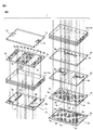
- 2 is an exploded perspective view showing a multilayer LC filter 100.
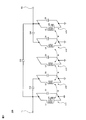
- FIG. 3 is an equivalent circuit diagram of the multilayer LC filter 100.
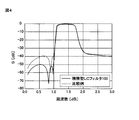
- FIG. It is a graph which shows the frequency characteristic of the multilayer LC filter 100, and the frequency characteristic of the multilayer LC filter concerning a comparative example.
- It is a disassembled perspective view which shows the lamination type LC filter 200 concerning 2nd Embodiment.
- 10 is an exploded perspective view showing a multilayer LC filter 1100 disclosed in Patent Document 1.
- each embodiment shows an embodiment of the present invention by way of example, and the present invention is not limited to the content of the embodiment. Moreover, it is also possible to implement combining the content described in different embodiment, and the implementation content in that case is also included in this invention. Further, the drawings are for helping understanding of the embodiment, and may not be drawn strictly. For example, a drawn component or a dimensional ratio between the components may not match the dimensional ratio described in the specification. In addition, the constituent elements described in the specification may be omitted in the drawings or may be drawn with the number omitted.
- FIG. 1 to 3 show a multilayer LC filter 100 according to the first embodiment.
- 1 is a perspective view
- FIG. 2 is an exploded perspective view
- FIG. 3 is an equivalent circuit diagram.
- the multilayer LC filter 100 includes a multilayer body 1.
- a pair of input / output terminals T ⁇ b> 1 and T ⁇ b> 2 are formed on opposite end surfaces of the laminate 1.
- Each of the input / output terminals T ⁇ b> 1 and T ⁇ b> 2 has one end extending to the lower main surface of the stacked body 1 and the other end extending to the upper main surface of the stacked body 1.
- a ground terminal G is formed on the lower main surface of the multilayer body 1.
- the laminate 1 is composed of, for example, 15 dielectric layers 1a to 1o made of ceramic, which are sequentially laminated from the bottom.
- each of the dielectric layers 1a to o constituting the multilayer body 1 will be described.
- Input / output terminals T1 and T2 are formed on opposite end surfaces of the dielectric layer 1a.
- input / output terminals T1 and T2 are formed on opposite end faces.
- the description and reference numerals are given to the drawings. May be omitted.
- a ground terminal G is formed on the lower main surface of the dielectric layer 1a.
- a ground conductor pattern 3 is formed on the upper main surface of the dielectric layer 1a.
- the ground conductor pattern 3 is connected to the ground terminal G by via conductors 2a to 2e.
- via conductors 2f to 2l are formed through the upper and lower main surfaces of the dielectric layer 1b.
- FIG. 2 which is an exploded perspective view, the via conductors 2f to 2l are depicted extending downward from the actual ones so that the connection relationship can be understood (the same applies to the via conductors described below). .
- the via conductors 2f to 2l are connected to the ground conductor pattern 3, respectively.
- the capacitor conductor pattern 4a is connected to the input / output terminal T1.
- the capacitor conductor pattern 4e is connected to the input / output terminal T2.
- the via conductors 2f to 2l are formed through the upper and lower main surfaces of the dielectric layer 1c.
- the via conductors 2f to 2l are also formed in the dielectric layer 1b as described above, but the via conductors with the same reference numerals formed in different dielectric layers mean that both are connected. .
- another five via conductors 2m to 2q are formed through the upper and lower main surfaces of the dielectric layer 1c.
- the via conductor 2m is connected to the capacitor conductor pattern 4a.
- the via conductor 2n is connected to the capacitor conductor pattern 4b.
- the via conductor 2o is connected to the capacitor conductor pattern 4c.
- the via conductor 2p is connected to the capacitor conductor pattern 4d.
- the via conductor 2q is connected to the capacitor conductor pattern 4e.
- Two capacitor conductor patterns 4f and 4g are formed on the upper main surface of the dielectric layer 1c.
- the capacitor conductor pattern 4f is connected to the via conductor 2m.
- the capacitor conductor pattern 4g is connected to the via conductor 2q.
- Two capacitor conductor patterns 4h and 4i are formed on the upper main surface of the dielectric layer 1d.
- the capacitor conductor pattern 4h and the capacitor conductor pattern 4i are connected to each other.
- Two line-shaped conductor patterns 5a and 5b are formed on the upper main surface of the dielectric layer 1i.
- the line-shaped conductor pattern 5a has one end connected to the midpoint X of the via conductor 2h and the other end connected to the via conductor 2f.
- the line-shaped conductor pattern 5b has one end connected to the midpoint Y of the via conductor 21 and the other end connected to the via conductor 2g.
- Ten via conductors 2h to 2q are formed in the four dielectric layers 1j to 1m so as to penetrate between the upper and lower main surfaces, respectively.
- the line-shaped conductor pattern 5c has one end connected to the via conductor 2h and the other end connected to the via conductor 2m.
- the line-shaped conductor pattern 5d has one end connected to the via conductor 2i and the other end connected to the via conductor 2n.
- the line-shaped conductor pattern 5e has one end connected to the via conductor 2j and the other end connected to the via conductor 2o.
- the line-shaped conductor pattern 5f has one end connected to the via conductor 2k and the other end connected to the via conductor 2p.
- the line-shaped conductor pattern 5g has one end connected to the via conductor 21 and the other end connected to the via conductor 2q.
- the dielectric layer 1o is a protective layer.
- Input / output terminals T1 and T2 are formed on opposite end faces of the dielectric layer 1o.
- the multilayer LC filter 100 having the above structure can be manufactured using materials and manufacturing methods that have been widely used in multilayer LC filters.
- the laminated LC filter 100 includes an equivalent circuit shown in FIG.
- the laminated LC filter 100 includes an input / output terminal T1 and an input / output terminal T2.
- first to fifth five LC resonators LC1 to LC5 are sequentially arranged between the input / output terminal T1 and the input / output terminal T2.
- the input / output terminal T1 is connected to the first LC resonator LC1.
- the input / output terminal T2 is connected to the fifth LC resonator LC5.
- the first LC resonator LC1 includes an inductor L1 and a capacitor C1 connected in parallel.
- the second LC resonator LC2 includes an inductor L2 and a capacitor C2
- the third LC resonator LC3 includes an inductor L3 and a capacitor C3
- the fourth LC resonator LC4 includes an inductor L4 and a capacitor C4.
- the fifth LC resonator LC5 includes an inductor L5 and a capacitor C5 connected in parallel.
- the first LC resonator LC1 is provided with a magnetic coupling adjusting inductor LX1 that is partially connected in parallel with the inductor L1. That is, the magnetic coupling adjusting inductor LX1 is connected between the midpoint of the inductor L1 and the ground.
- the fifth LC resonator LC5 is provided with a magnetic coupling adjusting inductor LX5 that is partially connected in parallel with the inductor L5. That is, the magnetic coupling adjusting inductor LX5 is connected between the midpoint of the inductor L5 and the ground.
- the inductor L1 and magnetic coupling adjusting inductor LX1 of the first LC resonator LC1 and the inductor L2 of the second LC resonator LC2 are magnetically coupled.
- the inductor L2 of the second LC resonator LC2 and the inductor L3 of the third LC resonator LC3 are magnetically coupled.
- the inductor L3 of the third LC resonator LC3 and the inductor L4 of the fourth LC resonator LC4 are magnetically coupled.
- the inductor L4 of the fourth LC resonator LC4, the inductor L5 of the fifth LC resonator LC5, and the magnetic coupling adjusting inductor LX5 are magnetically coupled.
- first LC resonator LC1 and the second LC resonator LC2 are capacitively coupled by the capacitor C12.
- fourth LC resonator LC4 and the fifth LC resonator LC5 are capacitively coupled by the capacitor C45.
- first LC resonator LC1 and the fifth LC resonator LC5 are capacitively coupled by the capacitor C15.
- the laminated LC filter 100 composed of the above equivalent circuit is a five-stage bandpass filter having a desired frequency characteristic by five LC resonators formed between the input / output terminal T1 and the input / output terminal T2. It is composed.
- the inductor L1 of the first LC resonator LC1 is configured by a loop inductor in which a via conductor 2m, a line-shaped conductor pattern 5c, and a via conductor 2h are connected.
- the via conductor 2m is connected to the capacitor conductor pattern 4a
- the via conductor 2h is connected to the ground conductor pattern 3.
- the capacitor C1 of the first LC resonator LC1 is constituted by a capacitance between the capacitor conductor pattern 4a and the ground conductor pattern 3.
- the capacitor conductor pattern 4a is connected to the input / output terminal T1 as described above.
- the magnetic coupling adjusting inductor LX1 of the first LC resonator LC1 is constituted by a line-shaped conductor pattern 5a and a via conductor 2f connected in series.
- the line-shaped conductor pattern 5a of the magnetic coupling adjusting inductor LX1 is connected to the midpoint X of the via conductor 2h, and the via conductor 2f is connected to the ground conductor pattern 3.
- the via conductor 2f of the magnetic coupling adjusting inductor LX1 of the first LC resonator LC1 is provided in the vicinity of the via conductor 2n of the inductor L2 of the second LC resonator LC2 described later.
- the line-shaped conductor pattern 5a of the magnetic coupling adjusting inductor LX1 and the line-shaped conductor pattern 5d of the inductor L2 of the second LC resonator LC2 are arranged in parallel to each other.
- the line-shaped conductor pattern 5a and the line-shaped conductor pattern 5d do not need to be arranged strictly in parallel, and may be arranged in a slightly inclined state. Then, by adjusting the angle formed between the line-shaped conductor pattern 5a and the line-shaped conductor pattern 5d, the strength of magnetic coupling between them can be adjusted.
- the inductor L2 of the second LC resonator LC2 is configured by a loop inductor in which a via conductor 2n, a line-shaped conductor pattern 5d, and a via conductor 2i are connected.
- the via conductor 2n is connected to the capacitor conductor pattern 4b, and the via conductor 2i is connected to the ground conductor pattern 3.
- the capacitor C2 of the second LC resonator LC2 is configured by a capacitance between the capacitor conductor pattern 4b and the ground conductor pattern 3.
- the inductor L3 of the third LC resonator LC3 is configured by a loop inductor in which a via conductor 2o, a line-shaped conductor pattern 5e, and a via conductor 2j are connected.
- the via conductor 2o is connected to the capacitor conductor pattern 4c, and the via conductor 2j is connected to the ground conductor pattern 3.
- the capacitor C3 of the third LC resonator LC3 is constituted by a capacitance between the capacitor conductor pattern 4c and the ground conductor pattern 3.
- the inductor L4 of the fourth LC resonator LC4 is configured by a loop inductor in which a via conductor 2p, a line-shaped conductor pattern 5f, and a via conductor 2k are connected.
- the via conductor 2p is connected to the capacitor conductor pattern 4d
- the via conductor 2k is connected to the ground conductor pattern 3.
- the capacitor C4 of the fourth LC resonator LC4 is constituted by a capacitance between the capacitor conductor pattern 4d and the ground conductor pattern 3.
- the inductor L5 of the fifth LC resonator LC5 is configured by a loop inductor in which a via conductor 2q, a line-shaped conductor pattern 5g, and a via conductor 21 are connected.
- the via conductor 2q is connected to the capacitor conductor pattern 4e, and the via conductor 21 is connected to the ground conductor pattern 3.
- the capacitor C5 of the fifth LC resonator LC5 is constituted by a capacitance between the capacitor conductor pattern 4e and the ground conductor pattern 3.
- the capacitor conductor pattern 4b is connected to the input / output terminal T2 as described above.
- the magnetic coupling adjusting inductor LX5 of the fifth LC resonator LC5 is constituted by a line-shaped conductor pattern 5b and a via conductor 2g connected in series.
- the line-shaped conductor pattern 5b of the magnetic coupling adjusting inductor LX5 is connected to the midpoint Y of the via conductor 21 and the via conductor 2g is connected to the ground conductor pattern 3.
- the via conductor 2g of the magnetic coupling adjusting inductor LX5 of the fifth LC resonator LC5 is provided in the vicinity of the via conductor 2p of the inductor L4 of the fourth LC resonator LC4.
- the line-shaped conductor pattern 5b of the magnetic coupling adjusting inductor LX5 and the line-shaped conductor pattern 5f of the inductor L4 of the fourth LC resonator LC4 are arranged in parallel to each other.
- the line-shaped conductor pattern 5b and the line-shaped conductor pattern 5f do not need to be arranged strictly in parallel, and may be arranged in a slightly inclined state. Then, by adjusting the angle formed between the line-shaped conductor pattern 5b and the line-shaped conductor pattern 5f, the strength of the magnetic coupling between them can be adjusted.
- the capacitor C12 is constituted by a capacitance formed between the capacitor conductor pattern 4f and the capacitor conductor pattern 4b. As described above, the capacitor conductor pattern 4f is connected to the via conductor 2m.
- the capacitor conductor pattern 4b is also a capacitor conductor pattern of the capacitor C2 of the second LC resonator LC2.
- the capacitor C15 includes a capacitance formed between the capacitor conductor pattern 4f and the capacitor conductor pattern 4h, and a capacitance formed between the capacitor conductor pattern 4i and the capacitor conductor pattern 4g.
- the capacitor conductor pattern 4f is connected to the via conductor 2m
- the capacitor conductor pattern 4h and the capacitor conductor pattern 4i are connected to each other
- the capacitor conductor pattern 4g is connected to the via conductor 2q.
- the capacitor C45 is configured by a capacitance formed between the capacitor conductor pattern 4g and the capacitor conductor pattern 4d. As described above, the capacitor conductor pattern 4g is connected to the via conductor 2q.
- the capacitor conductor pattern 4d is also a capacitor conductor pattern of the capacitor C4 of the fourth LC resonator LC4.
- the multilayer LC filter 100 includes the equivalent circuit shown in FIG.
- the winding directions of the loop inductors constituting the inductors L1 to L5 of the first to fifth LC resonators LC1 to LC5 are all the same. That is, when the laminated body 1 is seen through from the end surface side where the input / output terminal T1 is formed toward the end surface side where the input / output terminal T2 is formed, the via conductor 2m and the line-shaped conductor pattern 5c constituting the inductor L1 A loop inductor connected to the via conductor 2h, a loop inductor connected to the via conductor 2n constituting the inductor L2, the line-shaped conductor pattern 5d, and the via conductor 2i, and a via conductor 2o constituting the inductor L3 and the line-shaped Loop inductor in which conductor pattern 5e and via conductor 2j are connected, loop inductor in which via conductor 2p, line-shaped conductor pattern 5f, and via conductor 2k constituting inductor L4 are connected, and
- the inductors L1 to L5 of the first to fifth LC resonators LC1 to LC5 are large between adjacent ones. It is magnetically coupled with strength.
- the loop inductor of the inductor L1 of the first LC resonator LC1 and the loop inductor of the inductor L2 of the second LC resonator LC2 have the same winding direction and are magnetically coupled with great strength.
- the first LC resonator LC1 includes the magnetic coupling adjusting inductor LX1, and the magnetic coupling adjusting inductor LX1 weakens (reduces) the above-described strong magnetic coupling by a certain amount. Function.
- the magnetic coupling adjusting inductor LX1 is the first It functions to weaken (reduce) the magnetic coupling strength between the inductor (inductor L1 and magnetic coupling adjusting inductor LX1) of the LC resonator LC1 and the inductor (inductor L2) of the second LC resonator LC2. .
- the loop inductor of the inductor L4 of the fourth LC resonator LC4 and the loop inductor of the inductor L5 of the fifth LC resonator LC5 have the same winding direction and are magnetically coupled with great strength.
- the fifth LC resonator LC5 includes the magnetic coupling adjusting inductor LX5, and the magnetic coupling adjusting inductor LX5 weakens (reduces) the magnetic coupling having the large strength by a certain amount. Function.
- the magnetic coupling adjustment inductor LX5 It functions to weaken (reduce) the magnetic coupling strength between the inductor (inductor L4) of the LC resonator LC4 and the inductor (inductor L5 and magnetic coupling adjusting inductor LX5) of the fifth LC resonator LC5. .
- the multilayer LC filter 100 is adjacent to the multilayer LC filter 100 by providing the magnetic coupling adjusting inductors LX1 and LX5 instead of adjusting the distance between the inductor L1 and the inductor L2 or the distance between the inductor L4 and the inductor L5.
- the strength of the magnetic coupling between the inductors of the LC resonator is adjusted. Therefore, according to the multilayer LC filter 100, it is possible to adjust the magnetic coupling between the inductors of adjacent LC resonators without increasing the size, and to obtain a desired frequency characteristic.
- FIG. 4 shows the frequency characteristics of the multilayer LC filter 100.
- the magnetic coupling adjusting inductor LX1 line-shaped conductor pattern 5a, via conductor 2f
- magnetic coupling adjusting inductor LX5 line-shaped conductor pattern 5b, via conductor 2g
- the multilayer LC filter 100 has a larger attenuation than the multilayer LC filter of the comparative example on both the low frequency side and the high frequency side outside the passband, and has excellent frequency characteristics. It has.
- FIG. 5 shows a laminated LC filter 200 according to the second embodiment. However, FIG. 5 is an exploded perspective view of the multilayer LC filter 200.
- the multilayer LC filter 200 is a part of the configuration of the multilayer LC filter 100 according to the first embodiment. Specifically, in the multilayer LC filter 100, the winding directions of the loop inductors of the inductors L1 to L5 of the first to fifth LC resonators LC1 to LC5 are all the same. On the other hand, in the multilayer LC filter 200, the winding direction of the loop inductors of the inductors L3 to L4 of the second to third LC resonators LC2 to LC3 is reversed from that of the multilayer LC filter 100.
- the via conductor 2n constituting the inductor L2 is connected to the capacitor conductor pattern 4b and the via conductor 2i is connected to the ground conductor pattern 3. Then, this is changed, and the via conductor 12n formed at the same position as the via conductor 2n is connected to the ground conductor pattern 3, and the via conductor 12i formed at the same position as the via conductor 2i is connected to the capacitor conductor pattern 4b. did.
- the via conductor 2o constituting the inductor L3 is connected to the capacitor conductor pattern 4c, and the via conductor 2j is connected to the ground conductor pattern 3.
- the via conductor 12o formed at the same position as the via conductor 2o was connected to the ground conductor pattern 3, and the via conductor 12i formed at the same position as the via conductor 2j was connected to the capacitor conductor pattern 4c.
- the via conductor 2p constituting the inductor L4 is connected to the capacitor conductor pattern 4d, and the via conductor 2k is connected to the ground conductor pattern 3.
- the via conductor 12p formed at the same position as the via conductor 2p was connected to the ground conductor pattern 3, and the via conductor 12k formed at the same position as the via conductor 2k was connected to the capacitor conductor pattern 4d.
- the shapes of the capacitor conductor patterns 4b, 4c, and 4d were slightly changed in accordance with the change in the connection relationship. However, in order to facilitate understanding, the code indicating each was not changed.
- the loop inductor of the inductor L1 of the first LC resonator LC1 and the loop inductor of the inductor L2 of the second LC resonator LC2 have opposite winding directions and have a small strength. Magnetically coupled.
- the first LC resonator LC1 includes the magnetic coupling adjusting inductor LX1
- the magnetic coupling adjusting inductor LX1 includes a current flowing through the inductor L2 of the second LC resonator LC2. Current flows in the same direction as.
- the magnetic coupling adjusting inductor LX1 includes the inductor of the first LC resonator LC1 (inductor L1 and the magnetic coupling adjusting inductor LX1) and the inductor of the second LC resonator LC2 (inductor L2) as viewed comprehensively. ) To increase (increase) the strength of magnetic coupling.
- the loop inductor of the inductor L4 of the fourth LC resonator LC4 and the loop inductor of the inductor L5 of the fifth LC resonator LC5 have opposite winding directions and are small. It is magnetically coupled with strength.
- the fifth LC resonator LC5 includes the magnetic coupling adjusting inductor LX5, and the magnetic coupling adjusting inductor LX5 includes a current flowing through the inductor L4 of the fourth LC resonator LC4. Current flows in the same direction as.
- the magnetic coupling adjusting inductor LX5 includes the inductor of the fourth LC resonator LC4 (inductor L4) and the inductor of the fifth LC resonator LC5 (inductor L5 and magnetic coupling adjusting inductor LX5) as a whole. ) To increase (increase) the strength of magnetic coupling.
- the multilayer LC filter 200 according to the second embodiment also provides magnetic coupling between inductors of adjacent LC resonators without increasing the size of the multilayer body 1.
- the desired frequency characteristics can be obtained by adjusting.
- the multilayer LC filter 100 according to the first embodiment and the multilayer LC filter 200 according to the second embodiment have been described above.
- the present invention is not limited to the contents described above, and various modifications can be made in accordance with the spirit of the invention.
- a five-stage bandpass filter including five LC resonators is configured, but the type and number of stages of the filter are arbitrary, and are not limited to the above-described contents.
- the first LC resonator LC1 is provided with the magnetic coupling adjusting inductor LX1
- the fifth LC resonator LC5 is provided with the magnetic coupling adjusting inductor LX5.
- the number of magnetic coupling adjusting inductors to be provided and the LC resonators to be provided are arbitrary, and are not limited to those described above.
- a magnetic coupling adjusting inductor may be provided in both of two adjacent LC resonators.
- one magnetic coupling adjusting inductor may be provided inside the multilayer body 1, or three or more magnetic coupling adjusting inductors may be provided.
- the magnetic coupling adjusting inductor LX1 is connected between the via conductor 2h of the loop inductor of the first LC resonator LC1 and the ground conductor pattern 3.
- the connection of LX1 is not limited to this portion, and for example, between the via conductor 2m of the loop inductor of the first LC resonator LC1 and the ground conductor pattern 3, or the line of the first LC resonator LC1.
- a magnetic coupling adjusting inductor LX1 may be connected between the conductor pattern 5c and the ground conductor pattern 3.
- the magnetic coupling adjusting inductor LX5 is connected between the via conductor 21 and the ground conductor pattern 3 of the loop inductor of the fifth LC resonator LC5.
- the connection of the inductor LX5 is not limited to this portion.
- the inductor LX5 is connected between the via conductor 2q of the loop inductor of the fifth LC resonator LC5 and the ground conductor pattern 3, or of the fifth LC resonator LC5.
- a magnetic coupling adjusting inductor LX5 may be connected between the line-shaped conductor pattern 5g and the ground conductor pattern 3.
- the multilayer body 1 is composed of the dielectric layers 1a to 1o made of 15 ceramic layers.
- the material and the number of the dielectric layers are arbitrary, and the contents described above are as follows. It is not limited.
- the dielectric layers 1a to 1o may be formed of resin.
Landscapes
- Engineering & Computer Science (AREA)
- Power Engineering (AREA)
- Microelectronics & Electronic Packaging (AREA)
- Physics & Mathematics (AREA)
- Acoustics & Sound (AREA)
- Filters And Equalizers (AREA)
- Coils Or Transformers For Communication (AREA)
Abstract
大型化することなく、隣接するLC共振器のインダクタ間の磁気結合の強さが調整された積層型LCフィルタを提供する。 少なくとも1つのLC共振器に磁気結合調整用インダクタが設けられ、その磁気結合調整用インダクタは線路状導体パターン5aとビア導体2fとが接続されたものからなり、ビア導体2hの途中点Xに線路状導体パターン5aが接続され、かつ、ビア導体2fがグランド導体パターン3に接続され、磁気結合調整用インダクタが設けられたLC共振器のループインダクタおよび磁気結合調整用インダクタが、隣接する他のLC共振器のループインダクタと磁気結合するようにした。
Description
本発明は、積層体の内部に複数のLC共振器を備えた積層型LCフィルタに関し、さらに詳しくは、大型化することなく、隣接するLC共振器のインダクタ間の磁気結合の強さが調整された積層型LCフィルタに関する。
複数の誘電体層が積層された積層体の内部に、インダクタとキャパシタとからなるLC共振器が形成された積層型LCフィルタが、種々の電子機器に使用されている。
そのような積層型LCフィルタが、特許文献1(特開2012-23752号公報)に開示されている。
図6に、特許文献1に開示された積層型LCフィルタ(積層帯域通過フィルタ)1100を示す。
積層型LCフィルタ1100は、5層のセラミック層101a~101eが積層された積層体101を備える。
セラミック層(接地電極形成層)101aの上側主面には、グランド導体パターン(接地電極)102が形成されている。グランド導体パターン102は、積層体101の側面に形成されたグランド端子(接地端子;図示せず)と接続するための接続導体パターン102a、102bを備えている。
セラミック層(キャパシタ導体パターン形成層)101bの上側主面には、4つのキャパシタ導体パターン103a~103dが形成されている。また、セラミック層101bには、4つのビア導体(ビア電極)104a~104dが形成されている。
セラミック層(入出力電極形成層)101cの上側主面には、積層体101の対向する端面に形成された入出力端子(入出力電極;図示せず)に接続するための接続導体パターン105a、105bが形成されている。また、セラミック層101bには、前出の4つのビア導体104a~104dに加え、さらに6つのビア導体104e~104jが形成されている。
セラミック層(線路状導体パターン形成層)101dの上側主面には、4つの線路状導体パターン(線路電極)106a~106dが形成されている。また、セラミック層101dには、ビア導体104a~104hが形成されている。
セラミック層(外層)101eは、保護層であり、導体パターン、ビア導体は形成されていない。
積層体101の内部には、第1~第4の4つのLC共振器が形成されている。各LC共振器は、ループインダクタとキャパシタとが並列に接続された構成からなる。
第1のLC共振器は、ビア導体104eと、線路状導体パターン106aと、ビア導体104aとが接続されたループインダクタを備えている。また、キャパシタ導体パターン103aとグランド導体パターン102とで、キャパシタが構成されている。そして、上述したように、ループインダクタとキャパシタとが並列に接続されている。
同様に、第2のLC共振器は、並列に接続された、ビア導体104fと線路状導体パターン106bとビア導体104bとが接続されたループインダクタと、キャパシタ導体パターン103bとグランド導体パターン102とで構成されたキャパシタとを備えている。第3のLC共振器は、並列に接続された、ビア導体104gと線路状導体パターン106cとビア導体104cとが接続されたループインダクタと、キャパシタ導体パターン103cとグランド導体パターン102とで構成されたキャパシタとを備えている。第4のLC共振器は、並列に接続された、ビア導体104hと線路状導体パターン106dとビア導体104dとが接続されたループインダクタと、キャパシタ導体パターン103dとグランド導体パターン102とで構成されたキャパシタとを備えている。
なお、第1のLC共振器のキャパシタ導体パターン103aは、ビア導体104iおよび接続導体パターン105aを経由して、一方の入出力端子(図示せず)に接続されている。同様に、第4のLC共振器のキャパシタ導体パターン103dは、ビア導体104jおよび接続導体パターン105bを経由して、他方の入出力端子(図示せず)に接続されている。
積層型LCフィルタ1100においては、第1のLC共振器のループインダクタと第2のLC共振器のループインダクタとが磁気結合し、第2のLC共振器のループインダクタと第3のLC共振器のループインダクタとが磁気結合し、第3のLC共振器のループインダクタと第4のLC共振器のループインダクタとが磁気結合している。なお、磁気結合しているのは、隣接しているLC共振器のループインダクタ同士には限られず、離れたLC共振器のループインダクタ同士も磁気結合している。たとえば、第1のLC共振器のループインダクタは、第2のLC共振器のループインダクタだけではなく、第3のLC共振器のループインダクタや、第4のLC共振器のループインダクタとも磁気結合している。ただし、距離が離れるほど磁気結合の強さは小さくなる。
積層型LCフィルタ1100は、製品の設計段階において、隣接するLC共振器のループインダクタ間の磁気結合の強さを調整することにより、所望の周波数特性を発現させることができる。そして、隣接するLC共振器のループインダクタ間の磁気結合の強さの調整は、2つのループインダクタの間の距離を調整することによりおこなうことができる。たとえば、2つのループインダクタ間の磁気結合の強さを大きくしたい場合は、2つのループインダクタ間の距離を小さくすれば良い。逆に、2つのループインダクタ間の磁気結合の強さを小さくしたい場合は、2つのループインダクタ間の距離を大きくすれば良い。
しかしながら、2つのループインダクタの間の距離を調整して、2つのループインダクタ間の磁気結合の強さを調整する方法には、積層体101が大型化してしまうという問題があった。特に、2つのループインダクタ間の磁気結合の強さを小さくしたい場合は、2つのループインダクタ間の距離を大きくしなければならず、積層体101が大型化してしまうという問題があった。また、この方法は、LC共振器のループインダクタの形成位置をシフト(調整)できるように、積層体101の大きさに余裕をもたせておく必要があり、積層体101が大型化してしまうという問題があった。
本発明は上述した従来の課題を解決するためになされたものであり、その手段として本発明の積層型LCフィルタは、複数の誘電体層が積層された直方体状の積層体と、誘電体層の層間に形成された複数の線路状導体パターンと、誘電体層の層間に形成された複数のキャパシタ導体パターンと、誘電体層の層間に形成された少なくとも1つのグランド導体パターンと、誘電体層を貫通して形成された複数のビア導体と、を備え、積層体の内部に、インダクタとキャパシタとが並列に接続された複数のLC共振器が形成され、隣接するLC共振器のインダクタ同士が磁気結合し、LC共振器のインダクタが、線路状導体パターンと、その線路状導体パターンの両端に接続された1対のビア導体とで構成されたループインダクタを備え、そのループインダクタの一方のビア導体はキャパシタ導体パターンに接続され、そのループインダクタの他方のビア導体はグランド導体パターンに接続され、LC共振器のキャパシタが、キャパシタ導体パターンとグランド導体パターンとの間の容量により構成され、複数のLC共振器のうち、少なくとも1つのLC共振器に、磁気結合調整用インダクタが設けられ、磁気結合調整用インダクタが設けられたLC共振器は、ループインダクタの途中点に、磁気結合調整用インダクタの一端が接続され、かつ、磁気結合調整用インダクタの他端が、グランド導体パターンに接続され、磁気結合調整用インダクタが設けられたLC共振器のループインダクタおよび磁気結合調整用インダクタが、隣接する他のLC共振器のループインダクタと磁気結合するようにした。
磁気結合調整用インダクタが、線路状導体パターンとビア導体とが接続されたものからなり、磁気結合調整用インダクタが設けられたLC共振器は、ループインダクタのグランド導体パターンに接続された側のビア導体の途中点に、磁気結合調整用インダクタの線路状導体パターンが接続され、かつ、磁気結合調整用インダクタのビア導体が、グランド導体パターンに接続されたものとすることが好ましい。この場合には、磁気結合調整用インダクタが設けられたLC共振器のループインダクタの巻回方向と、磁気結合調整用インダクタの巻回方向とを、逆方向にすることが可能になるため、磁気結合調整用インダクタが設けられたLC共振器のインダクタ(ループインダクタおよび磁気結合調整用インダクタ)と、隣接する他のLC共振器のインダクタ(ループインダクタ)との磁気結合の強さの調整がしやすくなる。
磁気結合調整用インダクタが設けられたLC共振器のループインダクタの巻回方向と、隣接する他のLC共振器のループインダクタの巻回方向とが同一であり、磁気結合調整用インダクタが設けられたLC共振器の磁気結合調整用インダクタのビア導体が、隣接する他のLC共振器のループインダクタのキャパシタ導体パターンに接続された側のビア導体の近傍に設けられたものとすることができる。この場合には、磁気結合調整用インダクタが設けられたLC共振器のループインダクタの巻回方向と、隣接する他のLC共振器のループインダクタの巻回方向とが同一であるため、磁気結合調整用インダクタが設けられたLC共振器のループインダクタと、隣接する他のLC共振器のループインダクタとの磁気結合の強さは大きい。しかしながら、磁気結合調整用インダクタが設けられたLC共振器の磁気結合調整用インダクタに流れる電流の方向と、隣接する他のLC共振器のループインダクタに流れる電流の方向が逆になるため、磁気結合調整用インダクタを設けたことによって、総合的に見た、磁気結合調整用インダクタが設けられたLC共振器のインダクタ(ループインダクタおよび磁気結合調整用インダクタ)と、隣接する他のLC共振器のインダクタ(ループインダクタ)との磁気結合は、強さを弱める(小さくする)ように調整される。
あるいは、磁気結合調整用インダクタが設けられたLC共振器のループインダクタの巻回方向と、隣接する他のLC共振器のループインダクタの巻回方向とが逆であり、磁気結合調整用インダクタが設けられたLC共振器の磁気結合調整用インダクタのビア導体が、隣接する他のLC共振器のループインダクタのグランド導体パターンに接続された側のビア導体の近傍に設けられたものとすることができる。この場合には、磁気結合調整用インダクタが設けられたLC共振器のループインダクタの巻回方向と、隣接する他のLC共振器のループインダクタの巻回方向とが逆であるため、磁気結合調整用インダクタが設けられたLC共振器のループインダクタと、隣接する他のLC共振器のループインダクタとの磁気結合の強さは小さい。しかしながら、磁気結合調整用インダクタが設けられたLC共振器の磁気結合調整用インダクタに流れる電流の方向と、隣接する他のLC共振器のループインダクタに流れる電流の方向とが同じになるため、磁気結合調整用インダクタを設けたことによって、総合的に見た、磁気結合調整用インダクタが設けられたLC共振器のインダクタ(ループインダクタおよび磁気結合調整用インダクタ)と、隣接する他のLC共振器のインダクタ(ループインダクタ)との磁気結合は、強さを強める(大きくする)ように調整される。
本発明の積層型LCフィルタは、複数のLC共振器のうち、少なくとも1つのLC共振器に、磁気結合調整用インダクタを設けているため、積層体の大きさを大きくすることなく、その磁気結合調整用インダクタによって、総合的に見た、磁気結合調整用インダクタが設けられたLC共振器のインダクタ(ループインダクタおよび磁気結合調整用インダクタ)と、隣接する他のLC共振器のインダクタ(ループインダクタ)との磁気結合の強さを調整することができる。したがって、本発明の積層型LCフィルタは、積層体の大きさを大きくすることなく、所望の周波数特性を得ることができる。
以下、図面とともに、本発明を実施するための形態について説明する。
なお、各実施形態は、本発明の実施の形態を例示的に示したものであり、本発明が実施形態の内容に限定されることはない。また、異なる実施形態に記載された内容を組合せて実施することも可能であり、その場合の実施内容も本発明に含まれる。また、図面は、実施形態の理解を助けるためのものであり、必ずしも厳密に描画されていない場合がある。たとえば、描画された構成要素ないし構成要素間の寸法の比率が、明細書に記載されたそれらの寸法の比率と一致していない場合がある。また、明細書に記載されている構成要素が、図面において省略されている場合や、個数を省略して描画されている場合などがある。
[第1実施形態]
図1~図3に、第1実施形態にかかる積層型LCフィルタ100を示す。ただし、図1は斜視図、図2は分解斜視図、図3は等価回路図である。
図1~図3に、第1実施形態にかかる積層型LCフィルタ100を示す。ただし、図1は斜視図、図2は分解斜視図、図3は等価回路図である。
積層型LCフィルタ100は、積層体1を備える。
積層体1の対向する端面に、1対の入出力端子T1、T2が形成されている。入出力端子T1、T2は、それぞれ、一端が積層体1の下側主面に延出され、他端が積層体1の上側主面に延出されている。また、積層体1の下側主面に、グランド端子Gが形成されている。
積層体1は、図2に示すように、たとえばセラミックからなる15層の誘電体層1a~1oが下から順に積層されたものからなる。
以下において、まず、積層体1を構成する各誘電体層1a~oについて説明する。
誘電体層1aの対向する端面に、入出力端子T1、T2が形成されている。なお、以下に説明する誘電体層1b~1oにおいても、対向する端面に入出力端子T1、T2が形成されているが、特に必要がない場合には、その説明および図面への符号の付与を省略する場合がある。
誘電体層1aの下側主面に、グランド端子Gが形成されている
誘電体層1aの上下主面間を貫通して、5つのビア導体2a~2eが形成されている。
誘電体層1aの上側主面に、グランド導体パターン3が形成されている。グランド導体パターン3は、ビア導体2a~2eによって、グランド端子Gに接続されている。
誘電体層1bの上下主面間を貫通して、7本のビア導体2f~2lが形成されている。なお、分解斜視図である図2においては、接続関係が分かるように、ビア導体2f~2lを、それぞれ、実際よりも下方向に伸ばして描写している(以下に説明するビア導体において同じ)。ビア導体2f~2lは、それぞれ、グランド導体パターン3に接続されている。
誘電体層1bの上側主面に、5つのキャパシタ導体パターン4a~4eが形成されている。キャパシタ導体パターン4aは入出力端子T1に接続されている。また、キャパシタ導体パターン4eは入出力端子T2に接続されている。
誘電体層1cの上下主面間を貫通して、7本のビア導体2f~2lが形成されている。なお、ビア導体2f~2lは、上述したように誘電体層1bにも形成されているが、異なる誘電体層に形成された同じ符号のビア導体は、両者が接続されていることを意味する。また、誘電体層1cの上下主面間を貫通して、別の5本のビア導体2m~2qが形成されている。ビア導体2mは、キャパシタ導体パターン4aに接続されている。ビア導体2nは、キャパシタ導体パターン4bに接続されている。ビア導体2oは、キャパシタ導体パターン4cに接続されている。ビア導体2pは、キャパシタ導体パターン4dに接続されている。ビア導体2qは、キャパシタ導体パターン4eに接続されている。
誘電体層1cの上側主面に、2つのキャパシタ導体パターン4f、4gが形成されている。キャパシタ導体パターン4fは、ビア導体2mに接続されている。また、キャパシタ導体パターン4gは、ビア導体2qに接続されている。
誘電体層1dの上下主面間を貫通して、12本のビア導体2f~2qが形成されている。
誘電体層1dの上側主面に、2つのキャパシタ導体パターン4h、4iが形成されている。キャパシタ導体パターン4hとキャパシタ導体パターン4iとは、相互に接続されている。
4層の誘電体層1e~1hに、それぞれ、上下主面間を貫通して、12本のビア導体2f~2qが形成されている。
誘電体層1iの上下主面間を貫通して、12本のビア導体2f~2qが形成されている。
誘電体層1iの上側主面に、2つの線路状導体パターン5a、5bが形成されている。線路状導体パターン5aは、一端がビア導体2hの途中点Xに接続され、他端がビア導体2fに接続されている。また、線路状導体パターン5bは、一端がビア導体2lの途中点Yに接続され、他端がビア導体2gに接続されている。
4層の誘電体層1j~1mに、それぞれ、上下主面間を貫通して、10本のビア導体2h~2qが形成されている。
誘電体層1nの上下主面間を貫通して、10本のビア導体2h~2qが形成されている。
誘電体層1nの上側主面に、5つの線路状導体パターン5c~5gが、相互に、それぞれ所定の間隔を開けて、平行に形成されている。線路状導体パターン5cは、一端がビア導体2hに接続され、他端がビア導体2mに接続されている。線路状導体パターン5dは、一端がビア導体2iに接続され、他端がビア導体2nに接続されている。線路状導体パターン5eは、一端がビア導体2jに接続され、他端がビア導体2oに接続されている。線路状導体パターン5fは、一端がビア導体2kに接続され、他端がビア導体2pに接続されている。線路状導体パターン5gは、一端がビア導体2lに接続され、他端がビア導体2qに接続されている。
誘電体層1oは保護層である。誘電体層1oの対向する端面に、入出力端子T1、T2が形成されている。
以上の構造からなる積層型LCフィルタ100は、従来から積層型LCフィルタにおいて広く使用されている材料および製造方法を使用して、製造することができる。
積層型LCフィルタ100は、図3に示す等価回路を備えている。
積層型LCフィルタ100は、入出力端子T1と入出力端子T2と備える。
積層型LCフィルタ100は、入出力端子T1と入出力端子T2との間に、第1~第5の5つのLC共振器LC1~LC5が順に配置されている。入出力端子T1は、第1のLC共振器LC1に接続されている。入出力端子T2は、第5のLC共振器LC5に接続されている。
第1のLC共振器LC1は、インダクタL1とキャパシタC1とが並列に接続されたものからなる。同様に、第2のLC共振器LC2はインダクタL2とキャパシタC2とが、第3のLC共振器LC3はインダクタL3とキャパシタC3とが、第4のLC共振器LC4はインダクタL4とキャパシタC4とが、第5のLC共振器LC5はインダクタL5とキャパシタC5とが、それぞれ並列に接続されたものからなる。
第1のLC共振器LC1には、インダクタL1と部分的に並列に接続された、磁気結合調整用インダクタLX1が設けられている。すなわち、インダクタL1の途中点と、グランドとの間に、磁気結合調整用インダクタLX1が接続されている。
また、第5のLC共振器LC5には、インダクタL5と部分的に並列に接続された、磁気結合調整用インダクタLX5が設けられている。すなわち、インダクタL5の途中点と、グランドとの間に、磁気結合調整用インダクタLX5が接続されている。
そして、第1のLC共振器LC1のインダクタL1および磁気結合調整用インダクタLX1と、第2のLC共振器LC2のインダクタL2とが、磁気結合している。また、第2のLC共振器LC2のインダクタL2と、第3のLC共振器LC3のインダクタL3とが、磁気結合している。また、第3のLC共振器LC3のインダクタL3と、第4のLC共振器LC4のインダクタL4とが、磁気結合している。また、第4のLC共振器LC4のインダクタL4と、第5のLC共振器LC5のインダクタL5および磁気結合調整用インダクタLX5とが、磁気結合している。
また、第1のLC共振器LC1と第2のLC共振器LC2とが、キャパシタC12によって、容量結合している。また、第4のLC共振器LC4と第5のLC共振器LC5とが、キャパシタC45によって、容量結合している。また、第1のLC共振器LC1と第5のLC共振器LC5とが、キャパシタC15によって、容量結合している。
以上の等価回路からなる積層型LCフィルタ100は、入出力端子T1と入出力端子T2との間に形成された5つのLC共振器によって、所望の周波数特性を備えた5段のバンドパスフィルタを構成している。
次に、積層型LCフィルタ100の等価回路と構造との関係について説明する。
まず、第1のLC共振器LC1のインダクタL1は、ビア導体2mと、線路状導体パターン5cと、ビア導体2hとが接続されたループインダクタによって構成されている。なお、ビア導体2mはキャパシタ導体パターン4aに接続され、ビア導体2hはグランド導体パターン3に接続されている。また、第1のLC共振器LC1のキャパシタC1は、キャパシタ導体パターン4aとグランド導体パターン3との間の容量により構成されている。なお、キャパシタ導体パターン4aは、上述したとおり、入出力端子T1に接続されている。
また、第1のLC共振器LC1の磁気結合調整用インダクタLX1は、直列に接続された線路状導体パターン5aとビア導体2fとによって構成されている。なお、磁気結合調整用インダクタLX1の線路状導体パターン5aはビア導体2hの途中点Xに接続され、ビア導体2fはグランド導体パターン3に接続されている。
第1のLC共振器LC1の磁気結合調整用インダクタLX1のビア導体2fは、後述する第2のLC共振器LC2のインダクタL2のビア導体2nの近傍に設けられている。この結果、磁気結合調整用インダクタLX1の線路状導体パターン5aと、第2のLC共振器LC2のインダクタL2の線路状導体パターン5dとは、相互に平行に配置されている。ただし、線路状導体パターン5aと線路状導体パターン5dとは、厳密に平行に配置される必要はなく、多少傾いた状態で配置されても良い。そして、線路状導体パターン5aと線路状導体パターン5dとのなす角度を調整することにより、両者の磁気結合の強さを調整することもできる。
第2のLC共振器LC2のインダクタL2は、ビア導体2nと、線路状導体パターン5dと、ビア導体2iとが接続されたループインダクタによって構成されている。なお、ビア導体2nはキャパシタ導体パターン4bに接続され、ビア導体2iはグランド導体パターン3に接続されている。また、第2のLC共振器LC2のキャパシタC2は、キャパシタ導体パターン4bとグランド導体パターン3との間の容量により構成されている。
第3のLC共振器LC3のインダクタL3は、ビア導体2oと、線路状導体パターン5eと、ビア導体2jとが接続されたループインダクタによって構成されている。なお、ビア導体2oはキャパシタ導体パターン4cに接続され、ビア導体2jはグランド導体パターン3に接続されている。また、第3のLC共振器LC3のキャパシタC3は、キャパシタ導体パターン4cとグランド導体パターン3との間の容量により構成されている。
第4のLC共振器LC4のインダクタL4は、ビア導体2pと、線路状導体パターン5fと、ビア導体2kとが接続されたループインダクタによって構成されている。なお、ビア導体2pはキャパシタ導体パターン4dに接続され、ビア導体2kはグランド導体パターン3に接続されている。また、第4のLC共振器LC4のキャパシタC4は、キャパシタ導体パターン4dとグランド導体パターン3との間の容量により構成されている。
第5のLC共振器LC5のインダクタL5は、ビア導体2qと、線路状導体パターン5gと、ビア導体2lとが接続されたループインダクタによって構成されている。なお、ビア導体2qはキャパシタ導体パターン4eに接続され、ビア導体2lはグランド導体パターン3に接続されている。また、第5のLC共振器LC5のキャパシタC5は、キャパシタ導体パターン4eとグランド導体パターン3との間の容量により構成されている。なお、キャパシタ導体パターン4bは、上述したとおり、入出力端子T2に接続されている。
また、第5のLC共振器LC5の磁気結合調整用インダクタLX5は、直列に接続された線路状導体パターン5bとビア導体2gとによって構成されている。なお、磁気結合調整用インダクタLX5の線路状導体パターン5bはビア導体2lの途中点Yに接続され、ビア導体2gはグランド導体パターン3に接続されている。
第5のLC共振器LC5の磁気結合調整用インダクタLX5のビア導体2gは、第4のLC共振器LC4のインダクタL4のビア導体2pの近傍に設けられている。この結果、磁気結合調整用インダクタLX5の線路状導体パターン5bと、第4のLC共振器LC4のインダクタL4の線路状導体パターン5fとは、相互に平行に配置されている。ただし、線路状導体パターン5bと線路状導体パターン5fとは、厳密に平行に配置される必要はなく、多少傾いた状態で配置されても良い。そして、線路状導体パターン5bと線路状導体パターン5fとのなす角度を調整することにより、両者の磁気結合の強さを調整することもできる。
また、キャパシタC12は、キャパシタ導体パターン4fとキャパシタ導体パターン4bとの間に形成される容量により構成されている。上述したとおり、キャパシタ導体パターン4fは、ビア導体2mに接続されている。また、キャパシタ導体パターン4bは、第2のLC共振器LC2のキャパシタC2のキャパタ導体パターンでもある。
キャパシタC15は、キャパシタ導体パターン4fとキャパシタ導体パターン4hとの間に形成される容量、および、キャパシタ導体パターン4iとキャパシタ導体パターン4gとの間に形成される容量により構成されている。上述したとおり、キャパシタ導体パターン4fはビア導体2mに接続され、キャパシタ導体パターン4hとキャパシタ導体パターン4iとは相互に接続され、キャパシタ導体パターン4gはビア導体2qに接続されている。
キャパシタC45は、キャパシタ導体パターン4gとキャパシタ導体パターン4dとの間に形成される容量により構成されている。上述したとおり、キャパシタ導体パターン4gは、ビア導体2qに接続されている。また、キャパシタ導体パターン4dは、第4のLC共振器LC4のキャパシタC4のキャパタ導体パターンでもある。
以上の関係により、積層型LCフィルタ100は、積層体1の内部に、図3に示す等価回路が構成されている。
積層型LCフィルタ100は、第1~第5のLC共振器LC1~LC5のインダクタL1~L5を構成するループインダクタの巻回方向が全て同じである。すなわち、積層体1を、入出力端子T1が形成された端面側から入出力端子T2が形成された端面側に向かって透視した場合、インダクタL1を構成するビア導体2mと線路状導体パターン5cとビア導体2hとが接続されたループインダクタと、インダクタL2を構成するビア導体2nと線路状導体パターン5dとビア導体2iとが接続されたループインダクタと、インダクタL3を構成するビア導体2oと線路状導体パターン5eとビア導体2jとが接続されたループインダクタと、インダクタL4を構成するビア導体2pと線路状導体パターン5fとビア導体2kとが接続されたループインダクタと、インダクタL5を構成するビア導体2qと線路状導体パターン5gとビア導体2lとが接続されたループインダクタとは、全て同一の方向に巻回している。
積層型LCフィルタ100は、ループインダクタの巻回方向が全て同じであるため、第1~第5のLC共振器LC1~LC5のインダクタL1~L5は、それぞれ、隣接するもの同士の間で、大きな強さで磁気結合している。
たとえば、第1のLC共振器LC1のインダクタL1のループインダクタと、第2のLC共振器LC2のインダクタL2のループインダクタとは、巻回方向が同一であり、大きな強さで磁気結合している。しかしながら、第1のLC共振器LC1は、磁気結合調整用インダクタLX1を備えており、磁気結合調整用インダクタLX1は、上記の大きな強さの磁気結合を、一定量、弱める(小さくする)ように機能する。すなわち、磁気結合調整用インダクタLX1には、第2のLC共振器LC2のインダクタL2に流れる電流と逆方向に電流が流れるため、磁気結合調整用インダクタLX1は、総合的に見た、第1のLC共振器LC1のインダクタ(インダクタL1および磁気結合調整用インダクタLX1)と、第2のLC共振器LC2のインダクタ(インダクタL2)との磁気結合の強さを、弱める(小さくする)ように機能する。
同様に、第4のLC共振器LC4のインダクタL4のループインダクタと、第5のLC共振器LC5のインダクタL5のループインダクタとは、巻回方向が同一であり、大きな強さで磁気結合している。しかしながら、第5のLC共振器LC5は、磁気結合調整用インダクタLX5を備えており、磁気結合調整用インダクタLX5は、上記の大きな強さの磁気結合を、一定量、弱める(小さくする)ように機能する。すなわち、磁気結合調整用インダクタLX5には、第4のLC共振器LC4のインダクタL4に流れる電流と逆方向に電流が流れるため、磁気結合調整用インダクタLX5は、総合的に見た、第4のLC共振器LC4のインダクタ(インダクタL4)と、第5のLC共振器LC5のインダクタ(インダクタL5および磁気結合調整用インダクタLX5)との磁気結合の強さを、弱める(小さくする)ように機能する。
積層型LCフィルタ100は、インダクタL1とインダクタL2との間の距離や、インダクタL4とインダクタL5との間の距離を調整するのではなく、磁気結合調整用インダクタLX1、LX5を設けることにより、隣接するLC共振器のインダクタ間の磁気結合の強さを調整している。したがって、積層型LCフィルタ100によれば、大型化することなく、隣接するLC共振器のインダクタ間の磁気結合を調整し、所望の周波数特性を得ることができる。
図4に、積層型LCフィルタ100の周波数特性を示す。また、比較のために、積層型LCフィルタ100から、磁気結合調整用インダクタLX1(線路状導体パターン5a、ビア導体2f)および磁気結合調整用インダクタLX5(線路状導体パターン5b、ビア導体2g)を除去した、比較例にかかる積層型LCフィルタの周波数特性を示す。
図4から分かるように、積層型LCフィルタ100は、通過帯域の外側の低周波側および高周波側の両方において、比較例の積層型LCフィルタよりも減衰量が大きくなっており、優れた周波数特性を備えている。
[第2実施形態]
図5に、第2実施形態にかかる積層型LCフィルタ200を示す。ただし、図5は、積層型LCフィルタ200の分解斜視図である。
図5に、第2実施形態にかかる積層型LCフィルタ200を示す。ただし、図5は、積層型LCフィルタ200の分解斜視図である。
積層型LCフィルタ200は、第1実施形態にかかる積層型LCフィルタ100の構成の一部に変更を加えた。具体的には、積層型LCフィルタ100では、第1~第5のLC共振器LC1~LC5のインダクタL1~L5のループインダクタの巻回方向が全て同じであった。これに対し、積層型LCフィルタ200では、第2~第3のLC共振器LC2~LC3のインダクタL3~L4のループインダクタの巻回方向を、積層型LCフィルタ100と逆にした。
より具体的には、積層型LCフィルタ100では、インダクタL2を構成するビア導体2nをキャパシタ導体パターン4bに接続し、ビア導体2iをグランド導体パターン3に接続していたが、積層型LCフィルタ200では、これに変更を加え、ビア導体2nと同じ位置に形成されたビア導体12nをグランド導体パターン3に接続し、ビア導体2iと同じ位置に形成されたビア導体12iをキャパシタ導体パターン4bに接続した。同様に、積層型LCフィルタ100では、インダクタL3を構成するビア導体2oをキャパシタ導体パターン4cに接続し、ビア導体2jをグランド導体パターン3に接続していたが、積層型LCフィルタ200では、これに変更を加え、ビア導体2oと同じ位置に形成されたビア導体12oをグランド導体パターン3に接続し、ビア導体2jと同じ位置に形成されたビア導体12iをキャパシタ導体パターン4cに接続した。同様に、積層型LCフィルタ100では、インダクタL4を構成するビア導体2pをキャパシタ導体パターン4dに接続し、ビア導体2kをグランド導体パターン3に接続していたが、積層型LCフィルタ200では、これに変更を加え、ビア導体2pと同じ位置に形成されたビア導体12pをグランド導体パターン3に接続し、ビア導体2kと同じ位置に形成されたビア導体12kをキャパシタ導体パターン4dに接続した。
なお、積層型LCフィルタ200では、上記接続関係を変更したことにともない、キャパシタ導体パターン4b、4c、4dの形状を、それぞれ、若干、変更した。ただし、理解を容易にするために、それぞれを示す符号の変更はおこなわなかった。
積層型LCフィルタ200では、第1のLC共振器LC1のインダクタL1のループインダクタと、第2のLC共振器LC2のインダクタL2のループインダクタとは、巻回方向が逆であり、小さな強さで磁気結合している。しかしながら、積層型LCフィルタ200は、第1のLC共振器LC1が磁気結合調整用インダクタLX1を備えており、磁気結合調整用インダクタLX1には、第2のLC共振器LC2のインダクタL2に流れる電流と同じ方向に電流が流れる。したがって、磁気結合調整用インダクタLX1は、総合的に見た、第1のLC共振器LC1のインダクタ(インダクタL1および磁気結合調整用インダクタLX1)と、第2のLC共振器LC2のインダクタ(インダクタL2)との磁気結合の強さを、強める(大きくする)ように機能する。
同様に、積層型LCフィルタ200では、第4のLC共振器LC4のインダクタL4のループインダクタと、第5のLC共振器LC5のインダクタL5のループインダクタとは、巻回方向が逆であり、小さな強さで磁気結合している。しかしながら、積層型LCフィルタ200は、第5のLC共振器LC5が磁気結合調整用インダクタLX5を備えており、磁気結合調整用インダクタLX5には、第4のLC共振器LC4のインダクタL4に流れる電流と同じ方向に電流が流れる。したがって、磁気結合調整用インダクタLX5は、総合的に見た、第4のLC共振器LC4のインダクタ(インダクタL4)と、第5のLC共振器LC5のインダクタ(インダクタL5および磁気結合調整用インダクタLX5)との磁気結合の強さを、強める(大きくする)ように機能する。
第2実施形態にかかる積層型LCフィルタ200も、第1実施形態にかかる積層型LCフィルタ100と同様に、積層体1を大型化することなく、隣接するLC共振器のインダクタ間の磁気結合を調整して、所望の周波数特性を得ることができる。
以上、第1実施形態にかかる積層型LCフィルタ100と、第2実施形態にかかる積層型LCフィルタ200とについて説明した。しかしながら、本発明が上述した内容に限定されることはなく、発明の趣旨に沿って、種々の変更を加えることができる。
たとえば、積層型LCフィルタ100、200では、5つのLC共振器を備えた5段のバンドパスフィルタを構成したが、フィルタの種類や段数は任意であり、上述した内容には限定されない。
また、積層型LCフィルタ100、200では、いずれも、第1のLC共振器LC1に磁気結合調整用インダクタLX1を設け、第5のLC共振器LC5に磁気結合調整用インダクタLX5を設けた。しかしながら、設けられる磁気結合調整用インダクタの個数や、設けられる対象のLC共振器は任意であり、上述した内容には限定されない。たとえば、隣接する2つのLC共振器の両方に、磁気結合調整用インダクタを設けても良い。あるいは、積層体1の内部に1つの磁気結合調整用インダクタを設けたり、3つ以上の磁気結合調整用インダクタを設けたりしても良い。
また、積層型LCフィルタ100、200では、第1のLC共振器LC1のループインダクタのビア導体2hとグランド導体パターン3との間に磁気結合調整用インダクタLX1を接続したが、磁気結合調整用インダクタLX1を接続するのはこの部分には限定されず、たとえば、第1のLC共振器LC1のループインダクタのビア導体2mとグランド導体パターン3との間、あるいは、第1のLC共振器LC1の線路状導体パターン5cとグランド導体パターン3との間に、磁気結合調整用インダクタLX1を接続しても良い。同様に、積層型LCフィルタ100、200では、第5のLC共振器LC5のループインダクタのビア導体2lとグランド導体パターン3との間に磁気結合調整用インダクタLX5を接続したが、磁気結合調整用インダクタLX5を接続するのはこの部分には限定されず、たとえば、第5のLC共振器LC5のループインダクタのビア導体2qとグランド導体パターン3との間、あるいは、第5のLC共振器LC5の線路状導体パターン5gとグランド導体パターン3との間に、磁気結合調整用インダクタLX5を接続しても良い。
また、積層型LCフィルタ100、200では、積層体1を15層のセラミックからなる誘電体層1a~1oで構成したが、誘電体層の材質や層数は任意であり、上述した内容には限定されない。たとえば、誘電体層1a~1oを、樹脂によって形成しても良い。
1・・・積層体
1a~1o・・・誘電体層
2a~2q、12i~12k、12n~12p・・・ビア導体
3・・・グランド導体パターン
4a~4i・・・キャパシタ導体パターン
5a~5g・・・線路状導体パターン
T1、T2・・・入出力端子
G・・・グランド端子
LC1~LC5・・・LC共振器
L1~L5・・・インダクタ(ループインダクタ)
C1~C5、C12、C15、C45・・・キャパシタ
LX1、LX5・・・磁気結合調整用インダクタ
1a~1o・・・誘電体層
2a~2q、12i~12k、12n~12p・・・ビア導体
3・・・グランド導体パターン
4a~4i・・・キャパシタ導体パターン
5a~5g・・・線路状導体パターン
T1、T2・・・入出力端子
G・・・グランド端子
LC1~LC5・・・LC共振器
L1~L5・・・インダクタ(ループインダクタ)
C1~C5、C12、C15、C45・・・キャパシタ
LX1、LX5・・・磁気結合調整用インダクタ
Claims (4)
- 複数の誘電体層が積層された直方体状の積層体と、
前記誘電体層の層間に形成された複数の線路状導体パターンと、
前記誘電体層の層間に形成された複数のキャパシタ導体パターンと、
前記誘電体層の層間に形成された少なくとも1つのグランド導体パターンと、
前記誘電体層を貫通して形成された複数のビア導体と、を備え、
前記積層体の内部に、インダクタとキャパシタとが並列に接続された複数のLC共振器が形成され、隣接する前記LC共振器の前記インダクタ同士が磁気結合し、
前記LC共振器の前記インダクタが、前記線路状導体パターンと、当該線路状導体パターンの両端に接続された1対の前記ビア導体とで構成されたループインダクタを備え、当該ループインダクタの一方の前記ビア導体は前記キャパシタ導体パターンに接続され、当該ループインダクタの他方の前記ビア導体は前記グランド導体パターンに接続され、
前記LC共振器の前記キャパシタが、前記キャパシタ導体パターンと前記グランド導体パターンとの間の容量により構成された積層型LCフィルタであって、
複数の前記LC共振器のうち、少なくとも1つの前記LC共振器に、磁気結合調整用インダクタが設けられ、
前記磁気結合調整用インダクタが設けられた前記LC共振器は、前記ループインダクタの途中点に、前記磁気結合調整用インダクタの一端が接続され、かつ、前記磁気結合調整用インダクタの他端が、前記グランド導体パターンに接続され、
前記磁気結合調整用インダクタが設けられた前記LC共振器の前記ループインダクタおよび前記磁気結合調整用インダクタが、隣接する他の前記LC共振器の前記ループインダクタと磁気結合した積層型LCフィルタ。 - 前記磁気結合調整用インダクタが、前記線路状導体パターンと前記ビア導体とが接続されたものからなり、
前記磁気結合調整用インダクタが設けられた前記LC共振器は、前記ループインダクタの前記グランド導体パターンに接続された側の前記ビア導体の途中点に、前記磁気結合調整用インダクタの前記線路状導体パターンが接続され、かつ、前記磁気結合調整用インダクタの前記ビア導体が、前記グランド導体パターンに接続されている、請求項1に記載された積層型LCフィルタ。 - 前記磁気結合調整用インダクタが設けられた前記LC共振器の前記ループインダクタの巻回方向と、隣接する他の前記LC共振器の前記ループインダクタの巻回方向とが同一であり、
前記磁気結合調整用インダクタが設けられた前記LC共振器の前記磁気結合調整用インダクタの前記ビア導体が、隣接する他の前記LC共振器の前記ループインダクタの前記キャパシタ導体パターンに接続された側の前記ビア導体の近傍に設けられた、請求項1または2に記載された積層型LCフィルタ。 - 前記磁気結合調整用インダクタが設けられた前記LC共振器の前記ループインダクタの巻回方向と、隣接する他の前記LC共振器の前記ループインダクタの巻回方向とが逆であり、
前記磁気結合調整用インダクタが設けられた前記LC共振器の前記磁気結合調整用インダクタの前記ビア導体が、隣接する他の前記LC共振器の前記ループインダクタの前記グランド導体パターンに接続された側の前記ビア導体の近傍に設けられた、請求項1または2に記載された積層型LCフィルタ。
Priority Applications (3)
| Application Number | Priority Date | Filing Date | Title |
|---|---|---|---|
| CN201780061512.0A CN109845100B (zh) | 2016-10-05 | 2017-09-14 | 层叠型lc滤波器 |
| JP2018543816A JP6773122B2 (ja) | 2016-10-05 | 2017-09-14 | 積層型lcフィルタ |
| US16/368,908 US10771035B2 (en) | 2016-10-05 | 2019-03-29 | Multilayer LC filter |
Applications Claiming Priority (2)
| Application Number | Priority Date | Filing Date | Title |
|---|---|---|---|
| JP2016-197571 | 2016-10-05 | ||
| JP2016197571 | 2016-10-05 |
Related Child Applications (1)
| Application Number | Title | Priority Date | Filing Date |
|---|---|---|---|
| US16/368,908 Continuation US10771035B2 (en) | 2016-10-05 | 2019-03-29 | Multilayer LC filter |
Publications (1)
| Publication Number | Publication Date |
|---|---|
| WO2018066339A1 true WO2018066339A1 (ja) | 2018-04-12 |
Family
ID=61831742
Family Applications (1)
| Application Number | Title | Priority Date | Filing Date |
|---|---|---|---|
| PCT/JP2017/033356 Ceased WO2018066339A1 (ja) | 2016-10-05 | 2017-09-14 | 積層型lcフィルタ |
Country Status (5)
| Country | Link |
|---|---|
| US (1) | US10771035B2 (ja) |
| JP (1) | JP6773122B2 (ja) |
| CN (1) | CN109845100B (ja) |
| TW (1) | TWI643454B (ja) |
| WO (1) | WO2018066339A1 (ja) |
Cited By (1)
| Publication number | Priority date | Publication date | Assignee | Title |
|---|---|---|---|---|
| JP2024064086A (ja) * | 2022-10-27 | 2024-05-14 | Tdk株式会社 | 積層型電子部品 |
Families Citing this family (1)
| Publication number | Priority date | Publication date | Assignee | Title |
|---|---|---|---|---|
| JP7808497B2 (ja) * | 2022-03-24 | 2026-01-29 | Tdk株式会社 | 積層型フィルタ装置 |
Citations (4)
| Publication number | Priority date | Publication date | Assignee | Title |
|---|---|---|---|---|
| WO2007119356A1 (ja) * | 2006-04-14 | 2007-10-25 | Murata Manufacturing Co., Ltd. | 積層帯域通過フィルタ |
| JP2012105026A (ja) * | 2010-11-09 | 2012-05-31 | Murata Mfg Co Ltd | 積層型lcフィルタ |
| JP2015046788A (ja) * | 2013-08-28 | 2015-03-12 | 株式会社村田製作所 | 高周波部品 |
| WO2016152211A1 (ja) * | 2015-03-23 | 2016-09-29 | 株式会社村田製作所 | 帯域通過フィルタおよび積層型の帯域通過フィルタ |
Family Cites Families (9)
| Publication number | Priority date | Publication date | Assignee | Title |
|---|---|---|---|---|
| JP2000323908A (ja) * | 1999-05-07 | 2000-11-24 | Murata Mfg Co Ltd | 積層型lcフィルタ |
| JP3567885B2 (ja) * | 2000-11-29 | 2004-09-22 | 株式会社村田製作所 | 積層型lcフィルタ |
| US7671706B2 (en) | 2006-04-14 | 2010-03-02 | Murata Manufacturing Co., Ltd | High frequency multilayer bandpass filter |
| WO2011033878A1 (ja) * | 2009-09-18 | 2011-03-24 | 株式会社村田製作所 | フィルタ |
| CN103210585B (zh) | 2010-11-16 | 2015-09-02 | 株式会社村田制作所 | 层叠带通滤波器 |
| WO2013069419A1 (ja) * | 2011-11-09 | 2013-05-16 | 株式会社村田製作所 | 積層型lcフィルタ |
| US9123950B2 (en) * | 2013-09-26 | 2015-09-01 | Lg Chem, Ltd. | Battery module and battery cell |
| KR20150138977A (ko) * | 2014-05-30 | 2015-12-11 | 한국전자통신연구원 | 발광 소자 및 그의 제조방법 |
| WO2016092903A1 (ja) * | 2014-12-10 | 2016-06-16 | 株式会社村田製作所 | 電子部品 |
-
2017
- 2017-08-29 TW TW106129335A patent/TWI643454B/zh active
- 2017-09-14 WO PCT/JP2017/033356 patent/WO2018066339A1/ja not_active Ceased
- 2017-09-14 JP JP2018543816A patent/JP6773122B2/ja active Active
- 2017-09-14 CN CN201780061512.0A patent/CN109845100B/zh active Active
-
2019
- 2019-03-29 US US16/368,908 patent/US10771035B2/en active Active
Patent Citations (4)
| Publication number | Priority date | Publication date | Assignee | Title |
|---|---|---|---|---|
| WO2007119356A1 (ja) * | 2006-04-14 | 2007-10-25 | Murata Manufacturing Co., Ltd. | 積層帯域通過フィルタ |
| JP2012105026A (ja) * | 2010-11-09 | 2012-05-31 | Murata Mfg Co Ltd | 積層型lcフィルタ |
| JP2015046788A (ja) * | 2013-08-28 | 2015-03-12 | 株式会社村田製作所 | 高周波部品 |
| WO2016152211A1 (ja) * | 2015-03-23 | 2016-09-29 | 株式会社村田製作所 | 帯域通過フィルタおよび積層型の帯域通過フィルタ |
Cited By (1)
| Publication number | Priority date | Publication date | Assignee | Title |
|---|---|---|---|---|
| JP2024064086A (ja) * | 2022-10-27 | 2024-05-14 | Tdk株式会社 | 積層型電子部品 |
Also Published As
| Publication number | Publication date |
|---|---|
| US10771035B2 (en) | 2020-09-08 |
| TWI643454B (zh) | 2018-12-01 |
| CN109845100A (zh) | 2019-06-04 |
| TW201826701A (zh) | 2018-07-16 |
| CN109845100B (zh) | 2022-11-08 |
| JPWO2018066339A1 (ja) | 2019-07-25 |
| US20190229698A1 (en) | 2019-07-25 |
| JP6773122B2 (ja) | 2020-10-21 |
Similar Documents
| Publication | Publication Date | Title |
|---|---|---|
| JP4821910B2 (ja) | 積層帯域通過フィルタ | |
| JP4356803B2 (ja) | 積層帯域通過フィルタ | |
| JP5142985B2 (ja) | 積層帯域通過フィルタ | |
| JP5821914B2 (ja) | 高周波部品 | |
| JP5874718B2 (ja) | 周波数可変共振回路および周波数可変フィルタ | |
| JP4650530B2 (ja) | Lc複合部品 | |
| JP6677305B2 (ja) | 積層型lcフィルタ | |
| CN108390658B (zh) | 层叠型电子部件以及层叠型lc滤波器 | |
| JP7322968B2 (ja) | 積層型lcフィルタ | |
| WO2018083936A1 (ja) | 積層型lcフィルタ | |
| JP2018078450A (ja) | 積層型フィルタ | |
| JP4569571B2 (ja) | Lc複合部品 | |
| JP2008278360A (ja) | 積層型バンドパスフィルタ及びそれを用いたダイプレクサ | |
| JP4303693B2 (ja) | 積層型電子部品 | |
| WO2018066339A1 (ja) | 積層型lcフィルタ | |
| WO2017086195A1 (ja) | 積層型lcフィルタ | |
| WO2017199749A1 (ja) | 積層型lcフィルタ | |
| WO2017043321A1 (ja) | 積層型lcフィルタ | |
| WO2022113674A1 (ja) | ローパスフィルタ、積層型ローパスフィルタおよびフィルタ特性調整方法 | |
| JP6638709B2 (ja) | 積層型電子部品および積層型lcフィルタ | |
| JP2002344274A (ja) | バランス型lcフィルタ |
Legal Events
| Date | Code | Title | Description |
|---|---|---|---|
| 121 | Ep: the epo has been informed by wipo that ep was designated in this application |
Ref document number: 17858178 Country of ref document: EP Kind code of ref document: A1 |
|
| ENP | Entry into the national phase |
Ref document number: 2018543816 Country of ref document: JP Kind code of ref document: A |
|
| NENP | Non-entry into the national phase |
Ref country code: DE |
|
| 122 | Ep: pct application non-entry in european phase |
Ref document number: 17858178 Country of ref document: EP Kind code of ref document: A1 |