WO2018066322A1 - エピタキシャルシリコンウェーハおよびエピタキシャルシリコンウェーハの製造方法 - Google Patents
エピタキシャルシリコンウェーハおよびエピタキシャルシリコンウェーハの製造方法 Download PDFInfo
- Publication number
- WO2018066322A1 WO2018066322A1 PCT/JP2017/032846 JP2017032846W WO2018066322A1 WO 2018066322 A1 WO2018066322 A1 WO 2018066322A1 JP 2017032846 W JP2017032846 W JP 2017032846W WO 2018066322 A1 WO2018066322 A1 WO 2018066322A1
- Authority
- WO
- WIPO (PCT)
- Prior art keywords
- silicon wafer
- epitaxial
- film
- epitaxial silicon
- nitrogen concentration
- Prior art date
- Legal status (The legal status is an assumption and is not a legal conclusion. Google has not performed a legal analysis and makes no representation as to the accuracy of the status listed.)
- Ceased
Links
Images

Classifications
-
- H—ELECTRICITY
- H10—SEMICONDUCTOR DEVICES; ELECTRIC SOLID-STATE DEVICES NOT OTHERWISE PROVIDED FOR
- H10P—GENERIC PROCESSES OR APPARATUS FOR THE MANUFACTURE OR TREATMENT OF DEVICES COVERED BY CLASS H10
- H10P14/00—Formation of materials, e.g. in the shape of layers or pillars
- H10P14/60—Formation of materials, e.g. in the shape of layers or pillars of insulating materials
- H10P14/63—Formation of materials, e.g. in the shape of layers or pillars of insulating materials characterised by the formation processes
- H10P14/6326—Deposition processes
- H10P14/6349—Deposition of epitaxial materials
-
- H—ELECTRICITY
- H10—SEMICONDUCTOR DEVICES; ELECTRIC SOLID-STATE DEVICES NOT OTHERWISE PROVIDED FOR
- H10D—INORGANIC ELECTRIC SEMICONDUCTOR DEVICES
- H10D62/00—Semiconductor bodies, or regions thereof, of devices having potential barriers
- H10D62/50—Physical imperfections
- H10D62/57—Physical imperfections the imperfections being on the surface of the semiconductor body, e.g. the body having a roughened surface
-
- H—ELECTRICITY
- H10—SEMICONDUCTOR DEVICES; ELECTRIC SOLID-STATE DEVICES NOT OTHERWISE PROVIDED FOR
- H10D—INORGANIC ELECTRIC SEMICONDUCTOR DEVICES
- H10D30/00—Field-effect transistors [FET]
- H10D30/60—Insulated-gate field-effect transistors [IGFET]
- H10D30/791—Arrangements for exerting mechanical stress on the crystal lattice of the channel regions
- H10D30/797—Arrangements for exerting mechanical stress on the crystal lattice of the channel regions being in source or drain regions, e.g. SiGe source or drain
-
- H—ELECTRICITY
- H10—SEMICONDUCTOR DEVICES; ELECTRIC SOLID-STATE DEVICES NOT OTHERWISE PROVIDED FOR
- H10D—INORGANIC ELECTRIC SEMICONDUCTOR DEVICES
- H10D62/00—Semiconductor bodies, or regions thereof, of devices having potential barriers
- H10D62/01—Manufacture or treatment
- H10D62/021—Forming source or drain recesses by etching e.g. recessing by etching and then refilling
-
- H—ELECTRICITY
- H10—SEMICONDUCTOR DEVICES; ELECTRIC SOLID-STATE DEVICES NOT OTHERWISE PROVIDED FOR
- H10D—INORGANIC ELECTRIC SEMICONDUCTOR DEVICES
- H10D62/00—Semiconductor bodies, or regions thereof, of devices having potential barriers
- H10D62/80—Semiconductor bodies, or regions thereof, of devices having potential barriers characterised by the materials
- H10D62/82—Heterojunctions
- H10D62/822—Heterojunctions comprising only Group IV materials heterojunctions, e.g. Si/Ge heterojunctions
-
- H—ELECTRICITY
- H10—SEMICONDUCTOR DEVICES; ELECTRIC SOLID-STATE DEVICES NOT OTHERWISE PROVIDED FOR
- H10D—INORGANIC ELECTRIC SEMICONDUCTOR DEVICES
- H10D62/00—Semiconductor bodies, or regions thereof, of devices having potential barriers
- H10D62/80—Semiconductor bodies, or regions thereof, of devices having potential barriers characterised by the materials
- H10D62/83—Semiconductor bodies, or regions thereof, of devices having potential barriers characterised by the materials being Group IV materials, e.g. B-doped Si or undoped Ge
-
- H—ELECTRICITY
- H10—SEMICONDUCTOR DEVICES; ELECTRIC SOLID-STATE DEVICES NOT OTHERWISE PROVIDED FOR
- H10D—INORGANIC ELECTRIC SEMICONDUCTOR DEVICES
- H10D62/00—Semiconductor bodies, or regions thereof, of devices having potential barriers
- H10D62/80—Semiconductor bodies, or regions thereof, of devices having potential barriers characterised by the materials
- H10D62/83—Semiconductor bodies, or regions thereof, of devices having potential barriers characterised by the materials being Group IV materials, e.g. B-doped Si or undoped Ge
- H10D62/832—Semiconductor bodies, or regions thereof, of devices having potential barriers characterised by the materials being Group IV materials, e.g. B-doped Si or undoped Ge being Group IV materials comprising two or more elements, e.g. SiGe
-
- H—ELECTRICITY
- H10—SEMICONDUCTOR DEVICES; ELECTRIC SOLID-STATE DEVICES NOT OTHERWISE PROVIDED FOR
- H10P—GENERIC PROCESSES OR APPARATUS FOR THE MANUFACTURE OR TREATMENT OF DEVICES COVERED BY CLASS H10
- H10P14/00—Formation of materials, e.g. in the shape of layers or pillars
- H10P14/20—Formation of materials, e.g. in the shape of layers or pillars of semiconductor materials
- H10P14/34—Deposited materials, e.g. layers
- H10P14/3402—Deposited materials, e.g. layers characterised by the chemical composition
- H10P14/3414—Deposited materials, e.g. layers characterised by the chemical composition being group IIIA-VIA materials
- H10P14/3416—Nitrides
-
- H—ELECTRICITY
- H10—SEMICONDUCTOR DEVICES; ELECTRIC SOLID-STATE DEVICES NOT OTHERWISE PROVIDED FOR
- H10P—GENERIC PROCESSES OR APPARATUS FOR THE MANUFACTURE OR TREATMENT OF DEVICES COVERED BY CLASS H10
- H10P14/00—Formation of materials, e.g. in the shape of layers or pillars
- H10P14/60—Formation of materials, e.g. in the shape of layers or pillars of insulating materials
- H10P14/69—Inorganic materials
- H10P14/694—Inorganic materials composed of nitrides
- H10P14/6943—Inorganic materials composed of nitrides containing silicon
- H10P14/69433—Inorganic materials composed of nitrides containing silicon the material being a silicon nitride not containing oxygen, e.g. SixNy or SixByNz
-
- H—ELECTRICITY
- H10—SEMICONDUCTOR DEVICES; ELECTRIC SOLID-STATE DEVICES NOT OTHERWISE PROVIDED FOR
- H10P—GENERIC PROCESSES OR APPARATUS FOR THE MANUFACTURE OR TREATMENT OF DEVICES COVERED BY CLASS H10
- H10P90/00—Preparation of wafers not covered by a single main group of this subclass, e.g. wafer reinforcement
-
- H—ELECTRICITY
- H10—SEMICONDUCTOR DEVICES; ELECTRIC SOLID-STATE DEVICES NOT OTHERWISE PROVIDED FOR
- H10P—GENERIC PROCESSES OR APPARATUS FOR THE MANUFACTURE OR TREATMENT OF DEVICES COVERED BY CLASS H10
- H10P95/00—Generic processes or apparatus for manufacture or treatments not covered by the other groups of this subclass
- H10P95/40—Treatments of semiconductor bodies to modify their internal properties, e.g. to produce internal imperfections
- H10P95/402—Treatments of semiconductor bodies to modify their internal properties, e.g. to produce internal imperfections of silicon bodies
-
- H—ELECTRICITY
- H10—SEMICONDUCTOR DEVICES; ELECTRIC SOLID-STATE DEVICES NOT OTHERWISE PROVIDED FOR
- H10P—GENERIC PROCESSES OR APPARATUS FOR THE MANUFACTURE OR TREATMENT OF DEVICES COVERED BY CLASS H10
- H10P95/00—Generic processes or apparatus for manufacture or treatments not covered by the other groups of this subclass
- H10P95/90—Thermal treatments, e.g. annealing or sintering
-
- H—ELECTRICITY
- H10—SEMICONDUCTOR DEVICES; ELECTRIC SOLID-STATE DEVICES NOT OTHERWISE PROVIDED FOR
- H10W—GENERIC PACKAGES, INTERCONNECTIONS, CONNECTORS OR OTHER CONSTRUCTIONAL DETAILS OF DEVICES COVERED BY CLASS H10
- H10W20/00—Interconnections in chips, wafers or substrates
- H10W20/01—Manufacture or treatment
- H10W20/031—Manufacture or treatment of conductive parts of the interconnections
- H10W20/032—Manufacture or treatment of conductive parts of the interconnections of conductive barrier, adhesion or liner layers
- H10W20/052—Manufacture or treatment of conductive parts of the interconnections of conductive barrier, adhesion or liner layers by treatments not introducing additional elements therein
- H10W20/0526—Manufacture or treatment of conductive parts of the interconnections of conductive barrier, adhesion or liner layers by treatments not introducing additional elements therein by thermal treatment thereof
-
- H—ELECTRICITY
- H10—SEMICONDUCTOR DEVICES; ELECTRIC SOLID-STATE DEVICES NOT OTHERWISE PROVIDED FOR
- H10W—GENERIC PACKAGES, INTERCONNECTIONS, CONNECTORS OR OTHER CONSTRUCTIONAL DETAILS OF DEVICES COVERED BY CLASS H10
- H10W20/00—Interconnections in chips, wafers or substrates
- H10W20/01—Manufacture or treatment
- H10W20/031—Manufacture or treatment of conductive parts of the interconnections
- H10W20/032—Manufacture or treatment of conductive parts of the interconnections of conductive barrier, adhesion or liner layers
- H10W20/054—Manufacture or treatment of conductive parts of the interconnections of conductive barrier, adhesion or liner layers by selectively removing parts thereof
-
- H—ELECTRICITY
- H10—SEMICONDUCTOR DEVICES; ELECTRIC SOLID-STATE DEVICES NOT OTHERWISE PROVIDED FOR
- H10P—GENERIC PROCESSES OR APPARATUS FOR THE MANUFACTURE OR TREATMENT OF DEVICES COVERED BY CLASS H10
- H10P14/00—Formation of materials, e.g. in the shape of layers or pillars
- H10P14/20—Formation of materials, e.g. in the shape of layers or pillars of semiconductor materials
- H10P14/34—Deposited materials, e.g. layers
- H10P14/3438—Doping during depositing
Definitions
- the present invention relates to an epitaxial silicon wafer and a method for manufacturing an epitaxial silicon wafer.
- distortion may be added in the vicinity of the wafer surface, which is a device active layer, as a measure for improving device characteristics.
- a strained silicon wafer obtained by epitaxially growing a SiGe layer on a single crystal silicon substrate and epitaxially growing a strained Si layer on the SiGe layer, a wafer by surface nitriding instead of the SiGe layer, and an SOI wafer have been proposed. .
- the tensile strain is generated in the strained Si layer due to the SiGe layer having a larger lattice constant than that of Si, and this strain changes the band structure of Si and the degeneracy is released, thereby increasing the carrier mobility. For this reason, by using this strained Si layer as a channel region, the carrier movement speed can be increased by 1.5 times or more compared to the case of a semiconductor substrate using normal bulk silicon. Therefore, the strained silicon wafer is suitable for high-speed MOSFET, MODFET, HEMT and the like.
- An object of the present invention is to provide an epitaxial silicon wafer and an epitaxial silicon wafer manufacturing method capable of suppressing the occurrence of dislocations.
- the present inventors have found that when the nitrogen concentration on the surface of the epitaxial film is increased, the occurrence of dislocations can be suppressed even when film stress is generated due to the formation of a strained layer. And this reason was guessed as follows.
- a strained layer is formed in the epitaxial film, it is considered that a small dislocation is first generated at the interface between the strained layer and the epitaxial film due to the film stress at this time, and then this small dislocation extends to the epitaxial film. Therefore, it was speculated that when the nitrogen concentration of the epitaxial film is increased, nitrogen is fixed to small dislocations at the interface, and this fixing suppresses the extension of the dislocations to the epitaxial film.
- the present invention has been completed based on the above findings.
- the epitaxial silicon wafer of the present invention is an epitaxial silicon wafer in which an epitaxial film made of silicon is provided on the surface of the silicon wafer, and the nitrogen concentration of the epitaxial film surface is 5.0 ⁇ 10 13 atoms / cm. It is 3 or more.
- the epitaxial silicon wafer which can suppress generation
- the nitrogen concentration on the surface of the epitaxial film in the present invention is a nitrogen concentration obtained by measuring a depth profile with a secondary ion mass spectrometer (SIMS) at a depth of 80 nm to 200 nm, preferably at a position of 100 nm. Means. This is because, in SIMS measurement, the nitrogen concentration cannot be measured on the outermost surface of the silicon wafer due to the influence of sample contamination, so that this is excluded and the influence of inward diffusion is accurately determined.
- SIMS secondary ion mass spectrometer
- the nitrogen concentration at a position where the depth from the surface of the epitaxial film is 3 ⁇ m is preferably 5.0 ⁇ 10 13 atoms / cm 3 or more.
- the nitrogen concentration at the depth can be maintained at a level at which dislocation generation can be suppressed.
- a strained layer that generates a film stress of 10 MPa or more and 1000 MPa is provided on the surface of the epitaxial film.
- an epitaxial silicon wafer capable of increasing the speed of carrier movement and suppressing the occurrence of dislocations.
- the oxygen concentration of the silicon wafer is 10 ⁇ 10 17 atoms / cm 3 or more and 15 ⁇ 10 17 atoms / cm 3 or less (ASTM 1979).
- the epitaxial silicon wafer manufacturing method of the present invention includes an epitaxial film forming step of forming an epitaxial film composed of silicon on a surface of a silicon wafer in a gas atmosphere of trichlorosilane, and the epitaxial film is formed by the epitaxial film forming step. And a nitrogen concentration setting step of forming a nitride film on the epitaxial film by heat-treating the silicon wafer in a nitrogen atmosphere, and setting a nitrogen concentration on the surface of the epitaxial film using inward diffusion from the nitride film. It is characterized by.
- an epitaxial film may be formed on a silicon wafer having an increased nitrogen concentration, and outward diffusion from the silicon wafer may be used.
- the diffusion rate of nitrogen is relatively high, in such a method, the outwardly diffused nitrogen passes through the epitaxial film and escapes to the outside, and the nitrogen concentration on the surface of the epitaxial film cannot be sufficiently increased.
- the nitrogen concentration on the surface of the epitaxial film is reduced to a level at which dislocation generation can be suppressed even if a strained layer is formed. Can be increased.
- the epitaxial silicon wafer manufacturing method of the present invention includes a natural oxide film removing step of removing a natural oxide film on the surface of the epitaxial film before forming the nitride film, and the nitrogen concentration setting step includes removing the natural oxide film. It is preferable to be performed on a silicon wafer.
- an epitaxial silicon wafer is moved to a heat treatment apparatus for forming a nitride film
- a natural oxide film is formed on the surface. If a natural oxide film exists on the surface of the epitaxial film, inward diffusion of nitrogen into the epitaxial film may be hindered.
- nitrogen can be easily diffused inward into the epitaxial film by removing the natural oxide film on the surface of the epitaxial film before forming the nitride film.
- the natural oxide film removing step is heat-treated in any of an argon atmosphere, an ammonia atmosphere, and a hydrogen atmosphere using the same heat treatment apparatus as the nitrogen concentration setting step. Preferably, it is done.
- a nitride film can be formed without exposing the epitaxial film to an oxygen atmosphere by a simple method of changing the atmosphere of the heat treatment apparatus after removing the natural oxide film.
- the method includes a nitride film removing step for removing the entire nitride film.
- the nitride film is useful for adjusting the nitrogen concentration of the epitaxial film, but must be removed before forming the device.
- the nitride film removal process at the device manufacturer can be omitted.
- the epitaxial silicon wafer manufacturer can inspect the surface of the epitaxial film, and a product whose quality is guaranteed can be delivered to the device manufacturer.
- a strained layer forming step of forming a strained layer that generates a film stress of 10 MPa or more and 1000 MPa on the surface of the epitaxial film exposed after the nitride film removing step is provided.
- the heat treatment temperature X (° C.) is 850 ° C. or more and 1400 ° C. or less, and the heat treatment time Y (second) is 1 second or more, and
- the heat treatment is preferably performed so as to satisfy the following formula (1). Y ⁇ 1 ⁇ 10 34 exp ( ⁇ 0.084X) (1)
- the nitrogen concentration on the surface of the epitaxial film can be increased to a level at which dislocation generation can be suppressed even if a strained layer is formed by a simple method using only the above formula (1).
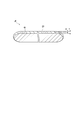
- FIG. 1 is a cross-sectional view of an epitaxial silicon wafer according to an embodiment of the present invention.
- the flowchart which shows the manufacturing method of the said epitaxial silicon wafer.
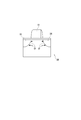
- Explanatory drawing which shows an example of the semiconductor substrate in which the distortion layer was formed in the device process with which the said epitaxial wafer is provided.
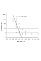
- the graph which shows the relationship between the temperature and time of heat processing in the nitrogen concentration setting process which concerns on the Example of this invention, and the presence or absence of a dislocation
- the epitaxial silicon wafer EW includes a silicon wafer WF and an epitaxial film EP provided on the surface of the silicon wafer WF.
- the film thickness T of the epitaxial film EP is preferably 0.1 ⁇ m or more and 20 ⁇ m or less.
- the reason why the thickness is preferably 0.1 ⁇ m or more is that the STI structure is generally formed at a depth of 0.1 ⁇ m or more from the surface of the epitaxial film EP.
- the reason why the thickness is preferably 20 ⁇ m or less is that when the thickness exceeds 20 ⁇ m, the influence of the warpage on the film stress due to the crystal lattice mismatch between the silicon wafer WF and the epitaxial film EP increases on the surface. This is because there is a possibility that the effect of suppressing dislocation due to the direction diffusion is reduced.
- the film thickness T is more preferably more than 3 ⁇ m and not more than 10 ⁇ m.
- the nitrogen concentration on the surface of the epitaxial film EP is preferably 5.0 ⁇ 10 13 atoms / cm 3 or more and 5.0 ⁇ 10 15 atoms / cm 3 or less, preferably 1 ⁇ 10 14 atoms / cm 3 or more and 3 ⁇ 10 15 atoms / cm 3. More preferred is cm 3 or less. It is preferable to introduce nitrogen below the solid solubility limit of the silicon crystal. However, since defects due to nitrogen may occur in the epitaxial film EP due to long-time heat treatment in the device process, the above concentration range is set. preferable.
- the measurement position of the nitrogen concentration is preferably a position where the depth D from the surface is 80 nm or more and 200 nm or less, and more preferably a position of 100 nm.
- the nitrogen concentration at a position where the depth D is 3 ⁇ m from the surface of the epitaxial film EP is preferably 5.0 ⁇ 10 13 atoms / cm 3 or more.
- the position where the depth D is 3 ⁇ m is within the epitaxial film EP when the film thickness T of the epitaxial film EP exceeds 3 ⁇ m, and is within the silicon wafer WF when the film thickness T is 3 ⁇ m or less.
- the nitrogen concentration at the position where the depth D is 3 ⁇ m is 5.0 ⁇ 10 13 atoms / cm 3 or more, the surface of the epitaxial film EP is temporarily treated by heat treatment or the like in the device process. Even when nitrogen escapes by outward diffusion, nitrogen is supplied to the surface of the epitaxial film EP from a position where the depth D is 3 ⁇ m, and dislocation can be suppressed.
- the oxygen concentration of the silicon wafer WF is preferably 10 ⁇ 10 17 atoms / cm 3 or more and 15 ⁇ 10 17 atoms / cm 3 or less (ASTM 1979). By setting the oxygen concentration within the above range, a sufficient strength of the epitaxial film EP can be obtained, and the occurrence of oxygen-induced defects can be suppressed in the epitaxial film EP.
- the manufacturing method of the epitaxial silicon wafer EW having the above characteristics includes a wafer preparation step S1, an epitaxial film formation step S2, a natural oxide film removal step S3, a nitrogen concentration setting step S4, and a nitride film.
- a removal step S5, a strained layer formation step S6, and a heat treatment step S7 are provided. Note that at least one of the natural oxide film removal step S3, the nitride film removal step S5, the strained layer formation step S6, and the heat treatment step S7 may not be performed.
- the wafer preparation step S1 is a process of slicing, chamfering, grinding, lapping, etching, polishing, cleaning the silicon single crystal ingot pulled up by the CZ (Czochralski) method, the MCZ (magnetic field applied Czochralski) method, etc.
- a silicon wafer WF whose surface is mirror-polished by a necessary process among heat treatments such as DK (donor killer) is prepared.
- an epitaxial film EP having a predetermined thickness T is formed on the silicon wafer WF to obtain an epitaxial silicon wafer EW.
- film formation is performed under a processing condition of 1150 ° C. or higher and 1280 ° C. or lower in a gas atmosphere such as trichlorosilane. Necessary dopants such as boron and phosphorus can also be added.
- the natural oxide film formed on the epitaxial film EP is removed.
- the epitaxial silicon wafer EW is placed in the heat treatment apparatus used in the nitrogen concentration setting step S4, and heat treatment is performed in any one of an argon atmosphere, an ammonia atmosphere, and a hydrogen atmosphere. Then, the natural oxide film may be removed.
- the heat treatment temperature is preferably 1000 ° C. or higher and 1350 ° C. or lower.
- the heat treatment time is preferably 1 second or more and 60 seconds or less. In order to completely remove the natural oxide film, it is preferable to perform a heat treatment for 1 second or longer. In view of productivity, the heat treatment time is preferably short.
- the heat treatment temperature is 1000 ° C. or higher and 1350 ° C. or lower, it is considered that the natural oxide film can be sufficiently removed by the heat treatment for 60 seconds or shorter.
- the epitaxial silicon wafer EW from which the natural oxide film has been removed is heat-treated in a nitrogen atmosphere to form a nitride film on the epitaxial film EP, and epitaxial diffusion is performed using inward diffusion from the nitride film.
- the nitrogen concentration on the surface of the film EP is set.
- the nitrogen concentration of the silicon wafer WF is also set.
- the heat treatment temperature X (° C.) is 850 ° C. or higher and 1400 ° C. or lower
- the heat treatment time Y (second) is 1 second or longer, and the following formula (1) is satisfied. It is preferable to carry out.
- the heat treatment method can be any method such as a batch type treatment in a vertical furnace or a rapid heating / cooling heat treatment in a single wafer furnace. Good.
- the atmosphere gas for the heat treatment may be ammonia alone or a mixed gas such as argon and ammonia.
- the heat treatment apparatus used in the nitrogen concentration setting step S4 is preferably the same as the natural oxide film removal step S3 because the nitride film can be formed only by changing the atmosphere of the heat treatment apparatus after the natural oxide film is removed.
- the entire nitride film used for setting the nitrogen concentration of the epitaxial film EP is removed.
- the surface side of the epitaxial film EP may be removed together with the nitride film.
- the nitrogen concentration on the surface of the epitaxial film EP after the removal needs to be maintained at a level at which dislocation generation can be suppressed during formation of the strained layer.
- Examples of the method for removing the nitride film include a method by polishing or etching.
- a strained layer that generates a film stress of 10 MPa or more and 1000 MPa is formed on the EP surface exposed after the nitride film removing step S5.
- the strained layer is partially formed on the EP surface and becomes part of the device.
- the strained layer is formed as the source region SC and the drain region DR except for the region directly below the gate region GT, and generates a film stress in the surface direction of the EP surface indicated by the arrow TE. It is composed of a SiGe film, SiC or the like.
- the strained layer is not limited to the configuration shown in FIG. 3 as long as it generates film stress, and the formation method thereof is not particularly limited. Note that the strained layer forming step S6 may be included in the device manufacturing process, and the epitaxial silicon wafer EW in the present embodiment is subjected to such a device process.
- the heat treatment step S7 is performed under substantially the same conditions as the heat treatment in the device step, for example. Since the nitrogen concentration on the EP surface is set in the above-described range, even when a film stress of 10 MPa or more and 1000 MPa is generated by the strained layer in this heat treatment step S7, the occurrence of dislocation can be suppressed.
- Example manufacturing method [Experimental Example 1] After being cut from a 300 mm silicon single crystal grown by the Czochralski method (CZ method), an epitaxial film was grown to a thickness of 2 ⁇ m at a temperature of about 1100 ° C. on a mirror-finished silicon wafer. . Thereafter, as shown in Table 1, a natural oxide film removal step was performed as necessary, and a heat treatment (nitrogen concentration setting step) under the conditions shown in the same table was performed in a nitrogen atmosphere. When the processing time was 180 seconds or less, it was processed in an RTA (Rapid Thermal Annealing) furnace, and when it was longer than 180 seconds, it was processed in a vertical furnace.
- RTA Rapid Thermal Annealing
- the nitrogen concentration was less than the detection lower limit.
- the nitrogen concentration setting step was performed under the same conditions as these and the natural oxide film removal step was also performed. From this, it was confirmed that by performing the natural oxide film removing step before the nitrogen concentration setting step, it becomes easy to inwardly diffuse nitrogen into the epitaxial film, and the nitrogen concentration can be increased to a desired level.
- the nitrogen concentration in the epitaxial film surface is also more than a detection lower limit.
- the nitrogen concentration decreases toward the surface of the epitaxial silicon wafer.
- a nitride film is formed on the surface of the epitaxial silicon wafer, and inward diffusion from there is performed. This is because the nitrogen concentration increases toward the surface layer for use.
- dislocation pits are detected under all conditions where the nitrogen concentration at a depth of 3 ⁇ m from the epitaxial film surface is below the detection lower limit, and under all conditions above the detection lower limit, dislocation pits are detected. Not detected. This is because when stress is applied to a line-shaped depression formed on the surface of a silicon wafer by a three-point bending test, stress is concentrated there and dislocation occurs. This is thought to be because the critical stress for the generation of dislocations increased, and as a result, the generation of dislocations was suppressed. In Examples 1 and 3, it can be estimated that the same result as in Table 1 is obtained because the nitrogen concentration is the same.
- dislocation generation can be suppressed by setting the nitrogen concentration at a depth of 3 ⁇ m from the epitaxial film surface to 5.0 ⁇ 10 13 atoms / cm 3 or more.
- the nitrogen concentration at the depth of 3 ⁇ m within the above range, even if the nitrogen on the surface of the epitaxial film escapes by outward diffusion due to heat treatment in the device process, the depth of 3 ⁇ m Since nitrogen is supplied from the position to the surface of the epitaxial film, a desired strength can be obtained, and as a result, the occurrence of dislocations can be suppressed.
- EP Epitaxial film
- EW Epitaxial silicon wafer
- WF Silicon wafer.
Abstract
トリクロロシランのガス雰囲気において、エピタキシャルシリコンウェーハの製造方法は、シリコンウェーハの表面にシリコンで構成されたエピタキシャル膜を形成するエピタキシャル膜形成工程と、エピタキシャル膜形成工程でエピタキシャル膜が形成されたシリコンウェーハを窒素雰囲気で熱処理してエピタキシャル膜上に窒化膜を形成し、この窒化膜からの内方拡散を利用してエピタキシャル膜表面の窒素濃度を設定する窒素濃度設定工程とを備えている。
Description
本発明は、エピタキシャルシリコンウェーハおよびエピタキシャルシリコンウェーハの製造方法に関する。
微細化が進むシリコンデバイスでは、デバイス特性の向上策として、デバイス活性層であるウェーハ表面近傍に歪みが付加されることがある。
例えば、単結晶シリコン基板上にSiGe層をエピタキシャル成長させ、当該SiGe層の上に歪みSi層をエピタキシャル成長させた歪みシリコンウェーハや、SiGe層に換えて表面窒化によるウェーハや、SOIウェーハが提案されている。
例えば、単結晶シリコン基板上にSiGe層をエピタキシャル成長させ、当該SiGe層の上に歪みSi層をエピタキシャル成長させた歪みシリコンウェーハや、SiGe層に換えて表面窒化によるウェーハや、SOIウェーハが提案されている。
上記歪みSi層には、Siに比べて格子定数が大きいSiGe層によって、引っ張り歪みが生じており、この歪みによって、Siのバンド構造が変化し縮退が解けてキャリア移動度が高まる。このため、この歪みSi層をチャネル領域として用いることによって、通常のバルクシリコンを用いた半導体基板の場合と比べて、1.5倍以上のキャリア移動の高速化が可能となる。したがって、歪みシリコンウェーハは、高速MOSFET、MODFET、HEMT等に好適である。
しかし、歪みシリコンウェーハでは、ウェーハ表面近傍に付加される歪みによって発生する膜応力は非常に大きいため、この歪みからウェーハ表面側に向けて転位が発生することがある。そこで、このような転位を抑制するための検討がなされている(例えば、特許文献1参照)。
特許文献1に記載の方法では、エピタキシャル成長後に酸素濃度設定熱処理を行い、バルクからの外方拡散と表面酸化膜からの内方拡散とを利用して、エピタキシャル膜表面の酸素濃度を高めることで強度向上を図っている。
しかし、近年三次元デバイス構造の採用によりエピタキシャル膜に付加される応力が増加しており、特許文献1のような酸素濃度を高める方法では、十分な強度を得られないおそれがある。
本発明の目的は、転位の発生を抑制できるエピタキシャルシリコンウェーハおよびエピタキシャルシリコンウェーハの製造方法を提供することにある。
本発明者らは、鋭意研究を重ねた結果、エピタキシャル膜表面の窒素濃度を高くすると、歪み層の形成により膜応力が発生しても、転位の発生を抑制できることを見出した。そして、この理由を以下のように推測した。
エピタキシャル膜に歪み層が形成されると、このときの膜応力により、まず、歪み層とエピタキシャル膜との界面で小さな転位が発生し、その後、この小さな転位がエピタキシャル膜に伸展すると考えられる。そこで、エピタキシャル膜の窒素濃度を高くすると、上記界面の小さな転位に窒素が固着し、この固着によりエピタキシャル膜への転位の伸展が抑制されると推測した。
本発明は、上記知見に基づき完成されたものである。
エピタキシャル膜に歪み層が形成されると、このときの膜応力により、まず、歪み層とエピタキシャル膜との界面で小さな転位が発生し、その後、この小さな転位がエピタキシャル膜に伸展すると考えられる。そこで、エピタキシャル膜の窒素濃度を高くすると、上記界面の小さな転位に窒素が固着し、この固着によりエピタキシャル膜への転位の伸展が抑制されると推測した。
本発明は、上記知見に基づき完成されたものである。
すなわち、本発明のエピタキシャルシリコンウェーハは、シリコンウェーハの表面にシリコンで構成されたエピタキシャル膜が設けられたエピタキシャルシリコンウェーハであって、前記エピタキシャル膜表面の窒素濃度が5.0×10¹³atoms/cm3以上であることを特徴とする。
本発明によれば、エピタキシャル膜に歪み層が形成されても転位発生を抑制可能なエピタキシャルシリコンウェーハを提供できる。
なお、本発明におけるエピタキシャル膜表面の窒素濃度とは、二次イオン質量分析装置(SIMS)でデプスプロファイルを測定した窒素濃度のうち、深さ80nm以上200nm以下の位置、好ましくは100nmの位置におけるものを意味する。これは、SIMS測定においては、シリコンウェーハ最表面においては試料汚染の影響により窒素濃度を測定できないためこれを排除するとともに、内方拡散による影響を正確に判定するという目的による。
なお、本発明におけるエピタキシャル膜表面の窒素濃度とは、二次イオン質量分析装置(SIMS)でデプスプロファイルを測定した窒素濃度のうち、深さ80nm以上200nm以下の位置、好ましくは100nmの位置におけるものを意味する。これは、SIMS測定においては、シリコンウェーハ最表面においては試料汚染の影響により窒素濃度を測定できないためこれを排除するとともに、内方拡散による影響を正確に判定するという目的による。
本発明のエピタキシャルシリコンウェーハにおいて、前記エピタキシャル膜表面からの深さが3μmでの位置の窒素濃度が5.0×10¹³atoms/cm3以上であることが好ましい。
本発明によれば、仮にデバイス工程における熱処理などで、エピタキシャル膜表面の窒素濃度が下がったとしても、上記深さでの窒素濃度を転位発生が抑制可能なレベルに維持できる。
本発明のエピタキシャルシリコンウェーハにおいて、前記エピタキシャル膜表面に、10MPa以上1000MPaの膜応力を生じる歪み層が設けられていることが好ましい。
本発明によれば、キャリア移動の高速化が可能かつ転位の発生が抑制されたエピタキシャルシリコンウェーハを提供できる。
本発明のエピタキシャルシリコンウェーハにおいて、前記シリコンウェーハの酸素濃度が10×1017atoms/cm3以上15×1017atoms/cm3以下(ASTM1979)であることが好ましい。
シリコンウェーハの酸素濃度が10×1017atoms/cm3未満の場合、エピタキシャル膜の十分な強度を得られないおそれがあり、15×1017atoms/cm3を超える場合、エピタキシャル膜において酸素起因の欠陥が発生するおそれがある。
本発明によれば、上記不具合の発生を抑制できる。
本発明によれば、上記不具合の発生を抑制できる。
本発明のエピタキシャルシリコンウェーハの製造方法は、トリクロロシランのガス雰囲気において、シリコンウェーハの表面にシリコンで構成されたエピタキシャル膜を形成するエピタキシャル膜形成工程と、前記エピタキシャル膜形成工程でエピタキシャル膜が形成されたシリコンウェーハを窒素雰囲気で熱処理して前記エピタキシャル膜上に窒化膜を形成し、この窒化膜からの内方拡散を利用して前記エピタキシャル膜表面の窒素濃度を設定する窒素濃度設定工程とを備えていることを特徴とする。
エピタキシャル膜表面の窒素濃度を高めるための方法としては、例えば窒素濃度を高めたシリコンウェーハにエピタキシャル膜を形成し、このシリコンウェーハからの外方拡散を利用することが考えられる。しかし、窒素の拡散速度は比較的速いため、このような方法では、外方拡散する窒素がエピタキシャル膜を通過して外部に抜けてしまい、エピタキシャル膜表面の窒素濃度を十分に高められない。
これに対し、本願発明では、エピタキシャル膜上に形成された窒化膜からの内方拡散を利用するため、エピタキシャル膜表面の窒素濃度を、歪み層が形成されても転位発生を抑制可能なレベルまで高めることができる。
これに対し、本願発明では、エピタキシャル膜上に形成された窒化膜からの内方拡散を利用するため、エピタキシャル膜表面の窒素濃度を、歪み層が形成されても転位発生を抑制可能なレベルまで高めることができる。
本発明のエピタキシャルシリコンウェーハの製造方法において、前記窒化膜形成前の前記エピタキシャル膜表面の自然酸化膜を除去する自然酸化膜除去工程を備え、前記窒素濃度設定工程は、前記自然酸化膜が除去されたシリコンウェーハに対して行われることが好ましい。
例えば、エピタキシャルシリコンウェーハを窒化膜形成用の熱処理装置に移動させるとき、エピタキシャル膜が酸素を含む雰囲気に曝されるとその表面には自然酸化膜が形成されてしまう。エピタキシャル膜表面に自然酸化膜が存在すると、エピタキシャル膜への窒素の内方拡散が阻害されるおそれがある。
本発明では、窒化膜形成前にエピタキシャル膜表面の自然酸化膜を除去することで、エピタキシャル膜へ窒素を内方拡散させやすくできる。
本発明では、窒化膜形成前にエピタキシャル膜表面の自然酸化膜を除去することで、エピタキシャル膜へ窒素を内方拡散させやすくできる。
本発明のエピタキシャルシリコンウェーハの製造方法において、前記自然酸化膜除去工程は、前記窒素濃度設定工程と同じ熱処理装置を用い、アルゴン雰囲気、アンモニア雰囲気、および、水素雰囲気のいずれかの雰囲気で熱処理して行われることが好ましい。
本発明によれば、自然酸化膜の除去後、熱処理装置の雰囲気を変更するだけの簡単な方法で、エピタキシャル膜を酸素雰囲気に曝すことなく窒化膜を形成できる。
本発明のエピタキシャルシリコンウェーハの製造方法において、前記窒化膜全体を除去する窒化膜除去工程を備えていることが好ましい。
窒化膜は、エピタキシャル膜の窒素濃度の調整に有用であるが、デバイス形成前に除去する必要がある。
本発明によれば、デバイス製造メーカでの窒化膜除去処理を省略できる。また、エピタキシャルシリコンウェーハ製造メーカにおいて、エピタキシャル膜表面の検査を行うことができ、品質が保証された製品をデバイス製造メーカに納品できる。
本発明によれば、デバイス製造メーカでの窒化膜除去処理を省略できる。また、エピタキシャルシリコンウェーハ製造メーカにおいて、エピタキシャル膜表面の検査を行うことができ、品質が保証された製品をデバイス製造メーカに納品できる。
本発明のエピタキシャルシリコンウェーハの製造方法において、前記窒化膜除去工程後に露出した前記エピタキシャル膜表面に、10MPa以上1000MPaの膜応力を生じる歪み層を形成する歪み層形成工程を備えていることが好ましい。
本発明のエピタキシャルシリコンウェーハの製造方法において、前記窒素濃度設定工程は、前記熱処理の温度X(℃)が850℃以上1400℃以下、前記熱処理の時間Y(秒)が1秒以上であり、かつ、以下の式(1)を満たすように、前記熱処理を行うことが好ましい。
Y≧1×1034exp(-0.084X) … (1)
Y≧1×1034exp(-0.084X) … (1)
本発明によれば、上記式(1)を用いるだけの簡単な方法で、エピタキシャル膜表面の窒素濃度を、歪み層が形成されても転位発生を抑制可能なレベルまで高めることができる。
本発明の一実施形態を、図面を参照して説明する。
[エピタキシャルシリコンウェーハの構成]
図1に示すように、エピタキシャルシリコンウェーハEWは、シリコンウェーハWFと、このシリコンウェーハWFの表面に設けられたエピタキシャル膜EPとを備えている。
[エピタキシャルシリコンウェーハの構成]
図1に示すように、エピタキシャルシリコンウェーハEWは、シリコンウェーハWFと、このシリコンウェーハWFの表面に設けられたエピタキシャル膜EPとを備えている。
エピタキシャル膜EPの膜厚Tは、0.1μm以上20μm以下が好ましい。0.1μm以上が好ましい理由は、一般的に、STI構造がエピタキシャル膜EPの表面から深さ0.1μm以上の位置に形成されるためである。また、20μm以下が好ましい理由は、20μmを超えるような厚さの場合、シリコンウェーハWFとエピタキシャル膜EPとの結晶格子不整合による、そりの膜応力への影響が表面で大きくなり、窒素の内方拡散による転位の抑制効果が低減してしまう可能性が考えられるためである。なお、膜厚Tは、3μmを超え10μm以下であることがさらに好ましい。
エピタキシャル膜EPの表面の窒素濃度は、5.0×10¹³atoms/cm3以上5.0×1015atoms/cm3以下が好ましく、1×1014atoms/cm3以上3×1015atoms/cm3以下がより好ましい。シリコン結晶の固溶限以下で窒素を導入することが好ましいが、エピタキシャル膜EPにデバイス工程での長時間の熱処理による窒素起因の欠陥が発生する場合もあるので、上記の濃度範囲とすることが好ましい。この窒素濃度の測定位置は、表面からの深さDが80nm以上200nm以下の位置が好ましく、100nmの位置がより好ましい。
また、エピタキシャル膜EPの表面から深さDが3μmの位置での窒素濃度は、5.0×10¹³atoms/cm3以上であることが好ましい。深さDが3μmの位置は、エピタキシャル膜EPの膜厚Tが3μmを超える場合は、エピタキシャル膜EP内となり、膜厚Tが3μm以下の場合は、シリコンウェーハWF内となる。
たとえ、シリコンウェーハWF内であっても、深さDが3μmの位置での窒素濃度が5.0×10¹³atoms/cm3以上あれば、仮に、デバイス工程における熱処理などでエピタキシャル膜EP表面の窒素が外方拡散で抜けた場合であっても、深さDが3μmの位置から窒素がエピタキシャル膜EP表面に供給され、転位を抑制することが可能となる。
たとえ、シリコンウェーハWF内であっても、深さDが3μmの位置での窒素濃度が5.0×10¹³atoms/cm3以上あれば、仮に、デバイス工程における熱処理などでエピタキシャル膜EP表面の窒素が外方拡散で抜けた場合であっても、深さDが3μmの位置から窒素がエピタキシャル膜EP表面に供給され、転位を抑制することが可能となる。
シリコンウェーハWFの酸素濃度は、10×1017atoms/cm3以上15×1017atoms/cm3以下(ASTM1979)であることが好ましい。酸素濃度を上記範囲に設定することで、エピタキシャル膜EPの十分な強度を得られ、エピタキシャル膜EPにおいて酸素起因の欠陥の発生を抑制できる。
[エピタキシャルシリコンウェーハの製造方法]
図2に示すように、上記特性を有するエピタキシャルシリコンウェーハEWの製造方法は、ウェーハ準備工程S1と、エピタキシャル膜形成工程S2と、自然酸化膜除去工程S3と、窒素濃度設定工程S4と、窒化膜除去工程S5と、歪み層形成工程S6と、熱処理工程S7とを備えている。
なお、自然酸化膜除去工程S3、窒化膜除去工程S5、歪み層形成工程S6、熱処理工程S7のうち、少なくとも1つの工程を行わなくてもよい。
図2に示すように、上記特性を有するエピタキシャルシリコンウェーハEWの製造方法は、ウェーハ準備工程S1と、エピタキシャル膜形成工程S2と、自然酸化膜除去工程S3と、窒素濃度設定工程S4と、窒化膜除去工程S5と、歪み層形成工程S6と、熱処理工程S7とを備えている。
なお、自然酸化膜除去工程S3、窒化膜除去工程S5、歪み層形成工程S6、熱処理工程S7のうち、少なくとも1つの工程を行わなくてもよい。
ウェーハ準備工程S1は、CZ(チョクラルスキー)法や、MCZ(磁場印加チョクラルスキー)法等によって、引き上げられたシリコン単結晶インゴットを、スライス、面取り、研削、ラッピング、エッチング、研磨、洗浄、DK(ドナーキラー)等の熱処理等のうち、必要な工程によって表面が鏡面研磨されたシリコンウェーハWFを準備する。
エピタキシャル膜形成工程S2は、所定の膜厚Tのエピタキシャル膜EPをシリコンウェーハWFに成膜して、エピタキシャルシリコンウェーハEWを得る。この際、トリクロロシラン等のガス雰囲気で、1150℃以上1280℃以下の処理条件で成膜を行う。なお、ボロン、リン等の必要なドーパントを添加することもできる。
自然酸化膜除去工程S3は、エピタキシャル膜EPに形成された自然酸化膜を除去する。自然酸化膜除去工程S3は、例えば、窒素濃度設定工程S4で用いる熱処理装置にエピタキシャルシリコンウェーハEWを投入し、アルゴン雰囲気と、アンモニア雰囲気と、水素雰囲気とのうちいずれか1つの雰囲気で熱処理を行って、自然酸化膜を除去してもよい。
アルゴン雰囲気、アンモニア雰囲気、水素雰囲気、あるいはこれらのうち少なくとも2つの混合雰囲気のいずれの場合であっても、熱処理温度は1000℃以上1350℃以下が好ましい。1000℃より温度が低い場合、自然酸化膜を完全に除去できない可能性があり、また、熱処理装置の制約を考慮すると、上限は1350℃となる。また、熱処理時間は、1秒以上60秒以下が好ましい。自然酸化膜を完全に除去するためには1秒以上の熱処理を施すことが好ましい。また、生産性を考慮すると熱処理時間は短い方が好ましい。熱処理温度を1000℃以上1350℃以下とした場合、60秒以下の熱処理で自然酸化膜を十分に除去できると考えられる。
アルゴン雰囲気、アンモニア雰囲気、水素雰囲気、あるいはこれらのうち少なくとも2つの混合雰囲気のいずれの場合であっても、熱処理温度は1000℃以上1350℃以下が好ましい。1000℃より温度が低い場合、自然酸化膜を完全に除去できない可能性があり、また、熱処理装置の制約を考慮すると、上限は1350℃となる。また、熱処理時間は、1秒以上60秒以下が好ましい。自然酸化膜を完全に除去するためには1秒以上の熱処理を施すことが好ましい。また、生産性を考慮すると熱処理時間は短い方が好ましい。熱処理温度を1000℃以上1350℃以下とした場合、60秒以下の熱処理で自然酸化膜を十分に除去できると考えられる。
窒素濃度設定工程S4は、自然酸化膜が除去されたエピタキシャルシリコンウェーハEWを、窒素雰囲気で熱処理してエピタキシャル膜EP上に窒化膜を形成し、この窒化膜からの内方拡散を利用してエピタキシャル膜EP表面の窒素濃度を設定する。このとき、エピタキシャル膜EP表面とその内部に加えて、シリコンウェーハWFの窒素濃度も設定される。
窒素濃度設定工程S4において、熱処理の温度X(℃)が850℃以上1400℃以下、熱処理の時間Y(秒)が1秒以上であり、かつ、以下の式(1)を満たすように、熱処理を行うことが好ましい。
Y≧1×1034exp(-0.084X) … (1)
窒素濃度設定工程S4において、熱処理の温度X(℃)が850℃以上1400℃以下、熱処理の時間Y(秒)が1秒以上であり、かつ、以下の式(1)を満たすように、熱処理を行うことが好ましい。
Y≧1×1034exp(-0.084X) … (1)
熱処理方式は、エピタキシャル膜EPの窒素濃度が上述の範囲に設定可能であれば、縦型炉によるバッチ式の処理や、枚葉炉における急速加熱・急速冷却熱処理等、いずれの方式であってもよい。熱処理の雰囲気ガスは、アンモニアのみでもよいし、アルゴンとアンモニアなどの混合ガスであってもよい。窒素濃度設定工程S4で用いる熱処理装置は、自然酸化膜の除去後、この熱処理装置の雰囲気を変更するだけで窒化膜を形成できることから、自然酸化膜除去工程S3と同じであることが好ましい。
窒化膜除去工程S5は、エピタキシャル膜EPの窒素濃度設定に利用した窒化膜全体を除去する。窒化膜除去工程S5は、窒化膜とともにエピタキシャル膜EPの表面側も除去してもよい。この場合、除去後におけるエピタキシャル膜EP表面の窒素濃度は、歪み層形成時の転位発生を抑制可能なレベルを維持する必要がある。窒化膜を除去する方法としては、研磨やエッチングによる方法が例示できる。
歪み層形成工程S6は、窒化膜除去工程S5後に露出したEP表面に10MPa以上1000MPaの膜応力を生じる歪み層を形成する。
歪み層は、EP表面に部分的に形成され、デバイスの一部分となる。具体的には、歪み層は、図3に示すように、ゲート領域GTの直下を除いて、ソース領域SC,ドレイン領域DRとして形成され、矢印TEで示すEP表面の面方向に膜応力を生じるSiGe膜、SiC等で構成されている。歪み層は、膜応力を発生するものであれば、図3に示す構成に限定されるものではなく、またその形成方法も特に限定されるものではない。
なお、歪み層形成工程S6はデバイス製造工程に含まれてもよく、本実施形態におけるエピタキシャルシリコンウェーハEWは、このようなデバイス工程に供される。
歪み層は、EP表面に部分的に形成され、デバイスの一部分となる。具体的には、歪み層は、図3に示すように、ゲート領域GTの直下を除いて、ソース領域SC,ドレイン領域DRとして形成され、矢印TEで示すEP表面の面方向に膜応力を生じるSiGe膜、SiC等で構成されている。歪み層は、膜応力を発生するものであれば、図3に示す構成に限定されるものではなく、またその形成方法も特に限定されるものではない。
なお、歪み層形成工程S6はデバイス製造工程に含まれてもよく、本実施形態におけるエピタキシャルシリコンウェーハEWは、このようなデバイス工程に供される。
熱処理工程S7は、例えばデバイス工程における熱処理とほぼ同じ条件で行われる。EP表面の窒素濃度が上述した範囲に設定されているため、この熱処理工程S7において、歪み層により10MPa以上1000MPaの膜応力が生じた場合でも、転位が発生することを抑制できる。
[実施形態の作用効果]
上述したように、エピタキシャルシリコンウェーハEWにおけるエピタキシャル膜EP表面の窒素濃度を5.0×10¹³atoms/cm3以上にしたため、エピタキシャル膜EPに歪み層が形成されても転位発生を抑制できる。
また、上記エピタキシャルシリコンウェーハEWの窒素濃度を設定する際に、エピタキシャル膜EP上に形成された窒化膜からの内方拡散を利用するため、エピタキシャル膜EP表面の窒素濃度を、転位発生を抑制可能なレベルまで高められる製造方法を提供できる。
上述したように、エピタキシャルシリコンウェーハEWにおけるエピタキシャル膜EP表面の窒素濃度を5.0×10¹³atoms/cm3以上にしたため、エピタキシャル膜EPに歪み層が形成されても転位発生を抑制できる。
また、上記エピタキシャルシリコンウェーハEWの窒素濃度を設定する際に、エピタキシャル膜EP上に形成された窒化膜からの内方拡散を利用するため、エピタキシャル膜EP表面の窒素濃度を、転位発生を抑制可能なレベルまで高められる製造方法を提供できる。
次に、本発明を実施例により更に詳細に説明するが、本発明はこれらの例によってなんら限定されるものではない。
[サンプルの製造方法]
〔実験例1〕
チョクラルスキー法(CZ法)により成長させた300mmシリコン単結晶から切り出された後、鏡面加工が施されたシリコンウェーハに、1100℃程度の温度で、エピタキシャル膜を2μmの厚さに成長させた。
その後、表1に示すように、必要に応じて自然酸化膜除去工程を実施し、窒素雰囲気で同表に示す条件の熱処理(窒素濃度設定工程)を実施した。処理時間が180秒以下の場合はRTA(Rapid Thermal Annealing)炉にて、180秒より長い場合は縦型炉にて処理した。熱処理後、形成した窒化膜を全て除去し、表1に示す25条件の実験例1のエピタキシャルシリコンウェーハを得た。
なお、自然酸化膜除去工程では、窒素濃度設定工程で用いた熱処理装置を用い、1000℃の水素雰囲気中で60秒の熱処理を行った。
〔実験例1〕
チョクラルスキー法(CZ法)により成長させた300mmシリコン単結晶から切り出された後、鏡面加工が施されたシリコンウェーハに、1100℃程度の温度で、エピタキシャル膜を2μmの厚さに成長させた。
その後、表1に示すように、必要に応じて自然酸化膜除去工程を実施し、窒素雰囲気で同表に示す条件の熱処理(窒素濃度設定工程)を実施した。処理時間が180秒以下の場合はRTA(Rapid Thermal Annealing)炉にて、180秒より長い場合は縦型炉にて処理した。熱処理後、形成した窒化膜を全て除去し、表1に示す25条件の実験例1のエピタキシャルシリコンウェーハを得た。
なお、自然酸化膜除去工程では、窒素濃度設定工程で用いた熱処理装置を用い、1000℃の水素雰囲気中で60秒の熱処理を行った。
〔実験例2,3〕
エピタキシャル膜を4μmの厚さに成長させたこと以外は、実験例1と同様のプロセスにより、表1に示す25条件の実験例2のエピタキシャルシリコンウェーハを得た。
エピタキシャル膜を6μmの厚さに成長させたこと以外は、実験例1と同様のプロセスにより、表1に示す25条件の実験例3のエピタキシャルシリコンウェーハを得た。
エピタキシャル膜を4μmの厚さに成長させたこと以外は、実験例1と同様のプロセスにより、表1に示す25条件の実験例2のエピタキシャルシリコンウェーハを得た。
エピタキシャル膜を6μmの厚さに成長させたこと以外は、実験例1と同様のプロセスにより、表1に示す25条件の実験例3のエピタキシャルシリコンウェーハを得た。

[評価]
〔エピタキシャルシリコンウェーハの窒素濃度〕
実験例1,2,3のプロセスにより準備したエピタキシャルシリコンウェーハのエピタキシャル膜表層、具体的には、エピタキシャル膜表面から深さ3μmの位置での窒素濃度をSIMSにより測定した。
測定結果は、実験例1,2,3で同じであった。その結果を表1に示す。
なお、実験例1のエピタキシャル膜の厚さは2μmであることから、表1の結果は、シリコンウェーハ内の窒素濃度である。また、実験例2,3のエピタキシャル膜の厚さはそれぞれ4,6μmであることから、表1の結果は、エピタキシャル膜内の窒素濃度である。検出下限は、5.0×10¹³atoms/cm3である。
〔エピタキシャルシリコンウェーハの窒素濃度〕
実験例1,2,3のプロセスにより準備したエピタキシャルシリコンウェーハのエピタキシャル膜表層、具体的には、エピタキシャル膜表面から深さ3μmの位置での窒素濃度をSIMSにより測定した。
測定結果は、実験例1,2,3で同じであった。その結果を表1に示す。
なお、実験例1のエピタキシャル膜の厚さは2μmであることから、表1の結果は、シリコンウェーハ内の窒素濃度である。また、実験例2,3のエピタキシャル膜の厚さはそれぞれ4,6μmであることから、表1の結果は、エピタキシャル膜内の窒素濃度である。検出下限は、5.0×10¹³atoms/cm3である。
表1に示すように、自然酸化膜除去工程を実施していない条件7,12,14,17,20,23では、窒素濃度が検出下限未満であった。一方、これらと同じ条件で窒素濃度設定工程を実施し、かつ、自然酸化膜除去工程も実施した条件8,13,15,18,21,24では、いずれも窒素濃度が検出下限以上であった。
このことから、窒素濃度設定工程前に自然酸化膜除去工程を実施することで、エピタキシャル膜へ窒素を内方拡散させやすくなり、窒素濃度を所望のレベルまで高められることが確認できた。
なお、表1の窒素濃度が検出下限以上の条件については、エピタキシャル膜表面での窒素濃度も検出下限以上であると推定できる。その理由は、以下の通りである。
シリコンウェーハからの外方拡散を利用する場合、エピタキシャルシリコンウェーハの表層側ほど窒素濃度が低くなってしまうが、本実施例ではエピタキシャルシリコンウェーハ表面に窒化膜を形成し、そこからの内方拡散を利用するため、表層側ほど窒素濃度は高くなるからである。
このことから、窒素濃度設定工程前に自然酸化膜除去工程を実施することで、エピタキシャル膜へ窒素を内方拡散させやすくなり、窒素濃度を所望のレベルまで高められることが確認できた。
なお、表1の窒素濃度が検出下限以上の条件については、エピタキシャル膜表面での窒素濃度も検出下限以上であると推定できる。その理由は、以下の通りである。
シリコンウェーハからの外方拡散を利用する場合、エピタキシャルシリコンウェーハの表層側ほど窒素濃度が低くなってしまうが、本実施例ではエピタキシャルシリコンウェーハ表面に窒化膜を形成し、そこからの内方拡散を利用するため、表層側ほど窒素濃度は高くなるからである。
〔エピタキシャルシリコンウェーハの転位発生抑制効果〕
実験例2のエピタキシャルシリコンウェーハに対し、応力負荷試験を行った。
まず、エピタキシャルシリコンウェーハから、長さ3cm、幅1.5cm程度の測定用サンプルを切り出した。次に、測定用サンプルの表面(エピタキシャル膜の表面)側に、深さ100nm、幅50μm、長さ1mmのライン状のくぼみを形成した。そして、測定用サンプルを支点間距離2cm、試験温度800℃にて3点曲げ試験を実施した。この際、2Nの荷重を加え、測定用サンプルの表面側に引張応力を作用させた。
その後、室温まで冷却した測定用サンプルに対し、ライトエッチングを1μm程度実施し、ライン状くぼみから発生した転位ピットの有無を光学顕微鏡により観察した。
その結果を表1に示す。なお、転位ピットが検出された場合を「NG」と表記し、検出されなかった場合を「OK」と表記した。
実験例2のエピタキシャルシリコンウェーハに対し、応力負荷試験を行った。
まず、エピタキシャルシリコンウェーハから、長さ3cm、幅1.5cm程度の測定用サンプルを切り出した。次に、測定用サンプルの表面(エピタキシャル膜の表面)側に、深さ100nm、幅50μm、長さ1mmのライン状のくぼみを形成した。そして、測定用サンプルを支点間距離2cm、試験温度800℃にて3点曲げ試験を実施した。この際、2Nの荷重を加え、測定用サンプルの表面側に引張応力を作用させた。
その後、室温まで冷却した測定用サンプルに対し、ライトエッチングを1μm程度実施し、ライン状くぼみから発生した転位ピットの有無を光学顕微鏡により観察した。
その結果を表1に示す。なお、転位ピットが検出された場合を「NG」と表記し、検出されなかった場合を「OK」と表記した。
表1に示すように、エピタキシャル膜表面から深さ3μmの位置での窒素濃度が検出下限未満の全ての条件で、転位ピットが検出されており、検出下限以上の全ての条件で、転位ピットが検出されなかった。
これは、シリコンウェーハ表面に形成したライン状くぼみに、3点曲げ試験により応力を負荷した際に、そこに応力が集中して転位が発生するが、窒素濃度が高い場合には、応力集中部で転位発生の臨界応力が増大し、その結果、転位発生が抑制されたためと考えられる。なお、実験例1,3でも、窒素濃度が同じであることから、表1と同じ結果が得られると推定できる。
以上のことから、エピタキシャル膜表面から深さ3μmの位置での窒素濃度を5.0×10¹³atoms/cm3以上にすることで、転位発生を抑制できることが確認できた。
また、深さ3μmの位置での窒素濃度を上述の範囲にすることで、仮に、デバイス工程における熱処理などでエピタキシャル膜表面の窒素が外方拡散で抜けた場合であっても、深さ3μmの位置から窒素がエピタキシャル膜表面に供給されるため、所望の強度を得ることができ、その結果、転位発生を抑制できると考えられる。
これは、シリコンウェーハ表面に形成したライン状くぼみに、3点曲げ試験により応力を負荷した際に、そこに応力が集中して転位が発生するが、窒素濃度が高い場合には、応力集中部で転位発生の臨界応力が増大し、その結果、転位発生が抑制されたためと考えられる。なお、実験例1,3でも、窒素濃度が同じであることから、表1と同じ結果が得られると推定できる。
以上のことから、エピタキシャル膜表面から深さ3μmの位置での窒素濃度を5.0×10¹³atoms/cm3以上にすることで、転位発生を抑制できることが確認できた。
また、深さ3μmの位置での窒素濃度を上述の範囲にすることで、仮に、デバイス工程における熱処理などでエピタキシャル膜表面の窒素が外方拡散で抜けた場合であっても、深さ3μmの位置から窒素がエピタキシャル膜表面に供給されるため、所望の強度を得ることができ、その結果、転位発生を抑制できると考えられる。
〔窒素濃度設定工程における熱処理条件の数式化〕
表1における自然酸化膜除去工程を実施していない条件7,12,14,17,20,23以外の条件について、図4に示すように、窒素濃度設定工程における熱処理の温度Xと時間Yとの関係をグラフ化した。このグラフ化に際し、3点曲げ試験結果が「NG」の場合を「×」で示し、「OK」の場合を「○」で示した。
そして、「OK」と「NG」との境界を表す近似直線を求めたところ、以下の式(2)が得られ、上記近似直線よりも左側が「NG」の範囲で、右側が「OK」の範囲となった。
Y=1×1034exp(-0.084X) … (2)
このことから、上記式(1)を満たすように、窒素濃度設定工程における熱処理を行うことで、エピタキシャル膜表面から深さ3μmの位置での窒素濃度を5.0×10¹³atoms/cm3以上にすることができることがわかった。
表1における自然酸化膜除去工程を実施していない条件7,12,14,17,20,23以外の条件について、図4に示すように、窒素濃度設定工程における熱処理の温度Xと時間Yとの関係をグラフ化した。このグラフ化に際し、3点曲げ試験結果が「NG」の場合を「×」で示し、「OK」の場合を「○」で示した。
そして、「OK」と「NG」との境界を表す近似直線を求めたところ、以下の式(2)が得られ、上記近似直線よりも左側が「NG」の範囲で、右側が「OK」の範囲となった。
Y=1×1034exp(-0.084X) … (2)
このことから、上記式(1)を満たすように、窒素濃度設定工程における熱処理を行うことで、エピタキシャル膜表面から深さ3μmの位置での窒素濃度を5.0×10¹³atoms/cm3以上にすることができることがわかった。
EP…エピタキシャル膜、EW…エピタキシャルシリコンウェーハ、WF…シリコンウェーハ。
Claims (10)
- シリコンウェーハの表面にシリコンで構成されたエピタキシャル膜が設けられたエピタキシャルシリコンウェーハであって、
前記エピタキシャル膜表面の窒素濃度が5.0×10¹³atoms/cm3以上であることを特徴とするエピタキシャルシリコンウェーハ。 - 請求項1に記載のエピタキシャルシリコンウェーハにおいて、
前記エピタキシャル膜表面からの深さが3μmでの位置の窒素濃度が5.0×10¹³atoms/cm3以上であることを特徴とするエピタキシャルシリコンウェーハ。 - 請求項1または請求項2に記載のエピタキシャルシリコンウェーハにおいて、
前記エピタキシャル膜表面に、10MPa以上1000MPaの膜応力を生じる歪み層が設けられていることを特徴とするエピタキシャルシリコンウェーハ。 - 請求項1から請求項3のいずれか一項に記載のエピタキシャルシリコンウェーハにおいて、
前記シリコンウェーハの酸素濃度が10×1017atoms/cm3以上15×1017atoms/cm3以下(ASTM 1979)であることを特徴とするエピタキシャルシリコンウェーハ。 - トリクロロシランのガス雰囲気において、シリコンウェーハの表面にシリコンで構成されたエピタキシャル膜を形成するエピタキシャル膜形成工程と、
前記エピタキシャル膜形成工程でエピタキシャル膜が形成されたシリコンウェーハを窒素雰囲気で熱処理して前記エピタキシャル膜上に窒化膜を形成し、この窒化膜からの内方拡散を利用して前記エピタキシャル膜表面の窒素濃度を設定する窒素濃度設定工程とを備えていることを特徴とするエピタキシャルシリコンウェーハの製造方法。 - 請求項5に記載のエピタキシャルシリコンウェーハの製造方法において、
前記窒化膜形成前の前記エピタキシャル膜表面の自然酸化膜を除去する自然酸化膜除去工程を備え、
前記窒素濃度設定工程は、前記自然酸化膜が除去されたシリコンウェーハに対して行われることを特徴とするエピタキシャルシリコンウェーハの製造方法。 - 請求項6に記載のエピタキシャルシリコンウェーハの製造方法において、
前記自然酸化膜除去工程は、前記窒素濃度設定工程と同じ熱処理装置を用い、アルゴン雰囲気、アンモニア雰囲気、および、水素雰囲気のいずれかの雰囲気で熱処理して行われることを特徴とするエピタキシャルシリコンウェーハの製造方法。 - 請求項5から請求項7のいずれか一項に記載のエピタキシャルシリコンウェーハの製造方法において、
前記窒化膜全体を除去する窒化膜除去工程を備えていることを特徴とするエピタキシャルシリコンウェーハの製造方法。 - 請求項8に記載のエピタキシャルシリコンウェーハの製造方法において、
前記窒化膜除去工程後に露出した前記エピタキシャル膜表面に、10MPa以上1000MPaの膜応力を生じる歪み層を形成する歪み層形成工程を備えていることを特徴とするエピタキシャルシリコンウェーハの製造方法。 - 請求項5から請求項9のいずれか一項に記載のエピタキシャルシリコンウェーハの製造方法において、
前記窒素濃度設定工程は、前記熱処理の温度X(℃)が850℃以上1400℃以下、前記熱処理の時間Y(秒)が1秒以上であり、かつ、以下の式(1)を満たすように、前記熱処理を行うことを特徴とするエピタキシャルシリコンウェーハの製造方法。
Y≧1×1034exp(-0.084X) … (1)
Priority Applications (6)
| Application Number | Priority Date | Filing Date | Title |
|---|---|---|---|
| CN202311786223.0A CN117747417A (zh) | 2016-10-07 | 2017-09-12 | 外延硅晶片及外延硅晶片的制造方法 |
| KR1020197011274A KR102183254B1 (ko) | 2016-10-07 | 2017-09-12 | 에피택셜 실리콘 웨이퍼 및 에피택셜 실리콘 웨이퍼 제조 방법 |
| CN201780061762.4A CN109891552A (zh) | 2016-10-07 | 2017-09-12 | 外延硅晶片及外延硅晶片的制造方法 |
| US16/339,941 US20200051817A1 (en) | 2016-10-07 | 2017-09-12 | Epitaxial silicon wafer and method for manufacturing epitaxial silicon wafer |
| DE112017005106.1T DE112017005106T5 (de) | 2016-10-07 | 2017-09-12 | Epitaktischer Siliziumwafer und Verfahren zur Herstellung von epitaktischem Siliziumwafer |
| US17/848,919 US11888036B2 (en) | 2016-10-07 | 2022-06-24 | Method for setting a nitrogen concentration of a silicon epitaxial film in manufacturing an epitaxial silicon wafer |
Applications Claiming Priority (2)
| Application Number | Priority Date | Filing Date | Title |
|---|---|---|---|
| JP2016198825A JP6299835B1 (ja) | 2016-10-07 | 2016-10-07 | エピタキシャルシリコンウェーハおよびエピタキシャルシリコンウェーハの製造方法 |
| JP2016-198825 | 2016-10-07 |
Related Child Applications (2)
| Application Number | Title | Priority Date | Filing Date |
|---|---|---|---|
| US16/339,941 A-371-Of-International US20200051817A1 (en) | 2016-10-07 | 2017-09-12 | Epitaxial silicon wafer and method for manufacturing epitaxial silicon wafer |
| US17/848,919 Division US11888036B2 (en) | 2016-10-07 | 2022-06-24 | Method for setting a nitrogen concentration of a silicon epitaxial film in manufacturing an epitaxial silicon wafer |
Publications (1)
| Publication Number | Publication Date |
|---|---|
| WO2018066322A1 true WO2018066322A1 (ja) | 2018-04-12 |
Family
ID=61756514
Family Applications (1)
| Application Number | Title | Priority Date | Filing Date |
|---|---|---|---|
| PCT/JP2017/032846 Ceased WO2018066322A1 (ja) | 2016-10-07 | 2017-09-12 | エピタキシャルシリコンウェーハおよびエピタキシャルシリコンウェーハの製造方法 |
Country Status (7)
| Country | Link |
|---|---|
| US (2) | US20200051817A1 (ja) |
| JP (1) | JP6299835B1 (ja) |
| KR (1) | KR102183254B1 (ja) |
| CN (2) | CN117747417A (ja) |
| DE (1) | DE112017005106T5 (ja) |
| TW (1) | TWI654331B (ja) |
| WO (1) | WO2018066322A1 (ja) |
Families Citing this family (2)
| Publication number | Priority date | Publication date | Assignee | Title |
|---|---|---|---|---|
| JP7342392B2 (ja) * | 2019-03-22 | 2023-09-12 | 株式会社Sumco | エピタキシャルシリコンウェーハの製造方法、および、エピタキシャルシリコンウェーハ |
| JP7173082B2 (ja) * | 2020-04-17 | 2022-11-16 | 信越半導体株式会社 | 気相成長用のシリコン単結晶基板、気相成長基板及びこれらの製造方法 |
Citations (6)
| Publication number | Priority date | Publication date | Assignee | Title |
|---|---|---|---|---|
| WO2005104208A1 (ja) * | 2004-04-23 | 2005-11-03 | Komatsu Electronic Metals Co., Ltd. | シリコン半導体基板の熱処理方法及び同方法で処理されたシリコン半導体基板 |
| JP2006086179A (ja) * | 2004-09-14 | 2006-03-30 | Toshiba Ceramics Co Ltd | 歪みシリコンウェーハおよびその製造方法 |
| JP2007073594A (ja) * | 2005-09-05 | 2007-03-22 | Sumco Corp | エピタキシャルシリコンウェーハの製造方法 |
| JP2007073820A (ja) * | 2005-09-08 | 2007-03-22 | Sumco Corp | エピタキシャルウェーハ及びその製造方法 |
| JP2009252920A (ja) * | 2008-04-04 | 2009-10-29 | Sumco Corp | エピタキシャルシリコンウェーハ及びその製造方法 |
| JP2013118388A (ja) * | 2012-12-19 | 2013-06-13 | Sumco Corp | エピタキシャルウェーハとその製造方法 |
Family Cites Families (33)
| Publication number | Priority date | Publication date | Assignee | Title |
|---|---|---|---|---|
| IT1216212B (it) * | 1986-10-29 | 1990-02-22 | S G S Microelettrica S P A | Strati epitassiali con quanti ta' controllate di azoto cresciuti su substrati di silicio |
| DE69617628T2 (de) * | 1995-09-18 | 2002-08-14 | Koninklijke Philips Electronics N.V., Eindhoven | Varicapdiode und verfahren zur herstellung |
| CN1236501C (zh) * | 1996-02-07 | 2006-01-11 | 松下电器产业株式会社 | 半导体器件及其制造方法 |
| US5872017A (en) * | 1997-01-24 | 1999-02-16 | Seh America, Inc. | In-situ epitaxial passivation for resistivity measurement |
| JP3886085B2 (ja) * | 1999-05-14 | 2007-02-28 | 株式会社東芝 | 半導体エピタキシャル基板の製造方法 |
| US6690043B1 (en) * | 1999-11-26 | 2004-02-10 | Kabushiki Kaisha Toshiba | Semiconductor device and method of manufacturing the same |
| JP2004356164A (ja) * | 2003-05-27 | 2004-12-16 | Toshiba Ceramics Co Ltd | 歪みシリコン基板ウエハの製造方法 |
| JP2006013119A (ja) * | 2004-06-25 | 2006-01-12 | Toshiba Ceramics Co Ltd | 歪みシリコン基板ウェーハ |
| JP2008088045A (ja) | 2006-09-05 | 2008-04-17 | Sumco Corp | シリコン単結晶の製造方法およびシリコンウェーハの製造方法 |
| JP5072460B2 (ja) | 2006-09-20 | 2012-11-14 | ジルトロニック アクチエンゲゼルシャフト | 半導体用シリコンウエハ、およびその製造方法 |
| JP5487565B2 (ja) * | 2008-06-19 | 2014-05-07 | 株式会社Sumco | エピタキシャルウェーハおよびその製造方法 |
| JP2010027959A (ja) * | 2008-07-23 | 2010-02-04 | Sumco Corp | 高抵抗simoxウェーハの製造方法 |
| SG161151A1 (en) | 2008-10-22 | 2010-05-27 | Semiconductor Energy Lab | Soi substrate and method for manufacturing the same |
| US7875930B2 (en) | 2009-02-16 | 2011-01-25 | Vanguard International Semiconductor Corporation | Semiconductor structure having an enlarged finger shaped region for reducing electric field density and method of manufacturing the same |
| US8263484B2 (en) | 2009-03-03 | 2012-09-11 | Sumco Corporation | High resistivity silicon wafer and method for manufacturing the same |
| US8754497B2 (en) | 2009-05-27 | 2014-06-17 | Texas Instruments Incorporated | Strained LDMOS and demos |
| US9502266B2 (en) | 2010-02-08 | 2016-11-22 | Sumco Corporation | Silicon wafer and method of manufacturing thereof, and method of manufacturing semiconductor device |
| KR101308137B1 (ko) | 2011-12-19 | 2013-09-13 | 창원대학교 산학협력단 | 디지털 영상 워터마킹 방법 |
| JP5545310B2 (ja) * | 2012-03-08 | 2014-07-09 | 三菱電機株式会社 | 炭化珪素エピタキシャルウエハの製造方法、および、炭化珪素エピタキシャルウエハ、ならびに、炭化珪素半導体装置 |
| JP6032963B2 (ja) | 2012-06-20 | 2016-11-30 | キヤノン株式会社 | Soi基板、soi基板の製造方法および半導体装置の製造方法 |
| JP5776670B2 (ja) * | 2012-11-13 | 2015-09-09 | 株式会社Sumco | エピタキシャルシリコンウェーハの製造方法、エピタキシャルシリコンウェーハ、および固体撮像素子の製造方法 |
| JP5776669B2 (ja) * | 2012-11-13 | 2015-09-09 | 株式会社Sumco | エピタキシャルシリコンウェーハの製造方法、エピタキシャルシリコンウェーハ、および固体撮像素子の製造方法 |
| TWI541864B (zh) * | 2012-12-06 | 2016-07-11 | 世創電子材料公司 | 磊晶晶圓及其製造方法 |
| JP5516713B2 (ja) * | 2012-12-19 | 2014-06-11 | 株式会社Sumco | エピタキシャルウェーハの製造方法 |
| JP2014189419A (ja) | 2013-03-26 | 2014-10-06 | Sumitomo Electric Ind Ltd | インゴット、炭化珪素基板およびインゴットの製造方法 |
| JP2014236120A (ja) | 2013-06-03 | 2014-12-15 | トヨタ自動車株式会社 | 半導体装置及びその製造方法 |
| US20150014706A1 (en) | 2013-07-15 | 2015-01-15 | Laurence P. Sadwick | Vertical Hetero Wide Bandgap Transistor |
| US20150228788A1 (en) * | 2014-02-13 | 2015-08-13 | United Microelectronics Corp. | Stress memorization process and semiconductor structure including contact etch stop layer |
| US9761701B2 (en) | 2014-05-01 | 2017-09-12 | Infineon Technologies Ag | Bipolar transistor |
| JP6455023B2 (ja) | 2014-08-27 | 2019-01-23 | セイコーエプソン株式会社 | 半導体装置及びその製造方法 |
| JP6245156B2 (ja) * | 2014-12-02 | 2017-12-13 | 信越半導体株式会社 | シリコンウェーハの評価方法 |
| JP6341083B2 (ja) * | 2014-12-25 | 2018-06-13 | 株式会社Sumco | エピタキシャルシリコンウェーハの製造方法 |
| US10020203B1 (en) | 2017-01-06 | 2018-07-10 | Sumco Corporation | Epitaxial silicon wafer |
-
2016
- 2016-10-07 JP JP2016198825A patent/JP6299835B1/ja active Active
-
2017
- 2017-09-12 CN CN202311786223.0A patent/CN117747417A/zh active Pending
- 2017-09-12 KR KR1020197011274A patent/KR102183254B1/ko active Active
- 2017-09-12 WO PCT/JP2017/032846 patent/WO2018066322A1/ja not_active Ceased
- 2017-09-12 DE DE112017005106.1T patent/DE112017005106T5/de active Pending
- 2017-09-12 US US16/339,941 patent/US20200051817A1/en not_active Abandoned
- 2017-09-12 CN CN201780061762.4A patent/CN109891552A/zh active Pending
- 2017-09-15 TW TW106131733A patent/TWI654331B/zh active
-
2022
- 2022-06-24 US US17/848,919 patent/US11888036B2/en active Active
Patent Citations (6)
| Publication number | Priority date | Publication date | Assignee | Title |
|---|---|---|---|---|
| WO2005104208A1 (ja) * | 2004-04-23 | 2005-11-03 | Komatsu Electronic Metals Co., Ltd. | シリコン半導体基板の熱処理方法及び同方法で処理されたシリコン半導体基板 |
| JP2006086179A (ja) * | 2004-09-14 | 2006-03-30 | Toshiba Ceramics Co Ltd | 歪みシリコンウェーハおよびその製造方法 |
| JP2007073594A (ja) * | 2005-09-05 | 2007-03-22 | Sumco Corp | エピタキシャルシリコンウェーハの製造方法 |
| JP2007073820A (ja) * | 2005-09-08 | 2007-03-22 | Sumco Corp | エピタキシャルウェーハ及びその製造方法 |
| JP2009252920A (ja) * | 2008-04-04 | 2009-10-29 | Sumco Corp | エピタキシャルシリコンウェーハ及びその製造方法 |
| JP2013118388A (ja) * | 2012-12-19 | 2013-06-13 | Sumco Corp | エピタキシャルウェーハとその製造方法 |
Also Published As
| Publication number | Publication date |
|---|---|
| US11888036B2 (en) | 2024-01-30 |
| US20220319851A1 (en) | 2022-10-06 |
| CN117747417A (zh) | 2024-03-22 |
| TWI654331B (zh) | 2019-03-21 |
| KR102183254B1 (ko) | 2020-11-25 |
| KR20190047095A (ko) | 2019-05-07 |
| JP6299835B1 (ja) | 2018-03-28 |
| DE112017005106T5 (de) | 2019-08-01 |
| CN109891552A (zh) | 2019-06-14 |
| US20200051817A1 (en) | 2020-02-13 |
| JP2018060959A (ja) | 2018-04-12 |
| TW201827635A (zh) | 2018-08-01 |
Similar Documents
| Publication | Publication Date | Title |
|---|---|---|
| US8343618B2 (en) | Silicon wafer and method of manufacturing the same | |
| US9991386B2 (en) | Epitaxial wafer and method of manufacturing the same | |
| JP5764937B2 (ja) | シリコン単結晶ウェーハの製造方法 | |
| JP7342392B2 (ja) | エピタキシャルシリコンウェーハの製造方法、および、エピタキシャルシリコンウェーハ | |
| CN105900219A (zh) | 硅晶片及其制备方法 | |
| CN106062926A (zh) | 外延硅晶片的制备方法及外延硅晶片 | |
| US11888036B2 (en) | Method for setting a nitrogen concentration of a silicon epitaxial film in manufacturing an epitaxial silicon wafer | |
| CN115135816A (zh) | 半导体硅晶片的制造方法 | |
| JP2001253795A (ja) | シリコンエピタキシャルウェーハとその製造方法 | |
| US20120049330A1 (en) | Silicon wafer and method for producing the same | |
| JP2025146998A (ja) | シリコンウェーハおよびエピタキシャルシリコンウェーハ | |
| JP2025157587A (ja) | シリコンウェーハおよびエピタキシャルシリコンウェーハ | |
| JP5704155B2 (ja) | エピタキシャルウェーハの製造方法 | |
| JP7757917B2 (ja) | シリコンウェーハおよびエピタキシャルシリコンウェーハ | |
| JP5516713B2 (ja) | エピタキシャルウェーハの製造方法 | |
| JP5655319B2 (ja) | シリコンウェーハ及びその製造方法、並びに、半導体デバイスの製造方法 | |
| CN105723497B (zh) | 外延硅片和外延硅片的制造方法 | |
| JP2023070019A (ja) | シリコンウェーハおよびエピタキシャルシリコンウェーハ | |
| JP6024710B2 (ja) | シリコンウェーハ及びその製造方法、並びに、半導体デバイスの製造方法 |
Legal Events
| Date | Code | Title | Description |
|---|---|---|---|
| 121 | Ep: the epo has been informed by wipo that ep was designated in this application |
Ref document number: 17858161 Country of ref document: EP Kind code of ref document: A1 |
|
| ENP | Entry into the national phase |
Ref document number: 20197011274 Country of ref document: KR Kind code of ref document: A |
|
| 122 | Ep: pct application non-entry in european phase |
Ref document number: 17858161 Country of ref document: EP Kind code of ref document: A1 |