WO2018066176A1 - 電力変換装置及び電流歪の低減方法 - Google Patents
電力変換装置及び電流歪の低減方法 Download PDFInfo
- Publication number
- WO2018066176A1 WO2018066176A1 PCT/JP2017/021713 JP2017021713W WO2018066176A1 WO 2018066176 A1 WO2018066176 A1 WO 2018066176A1 JP 2017021713 W JP2017021713 W JP 2017021713W WO 2018066176 A1 WO2018066176 A1 WO 2018066176A1
- Authority
- WO
- WIPO (PCT)
- Prior art keywords
- current
- gain
- reactor
- value
- voltage
- Prior art date
- Legal status (The legal status is an assumption and is not a legal conclusion. Google has not performed a legal analysis and makes no representation as to the accuracy of the status listed.)
- Ceased
Links
Images


Classifications
-
- H—ELECTRICITY
- H02—GENERATION; CONVERSION OR DISTRIBUTION OF ELECTRIC POWER
- H02M—APPARATUS FOR CONVERSION BETWEEN AC AND AC, BETWEEN AC AND DC, OR BETWEEN DC AND DC, AND FOR USE WITH MAINS OR SIMILAR POWER SUPPLY SYSTEMS; CONVERSION OF DC OR AC INPUT POWER INTO SURGE OUTPUT POWER; CONTROL OR REGULATION THEREOF
- H02M3/00—Conversion of DC power input into DC power output
- H02M3/02—Conversion of DC power input into DC power output without intermediate conversion into AC
- H02M3/04—Conversion of DC power input into DC power output without intermediate conversion into AC by static converters
- H02M3/10—Conversion of DC power input into DC power output without intermediate conversion into AC by static converters using discharge tubes with control electrode or semiconductor devices with control electrode
- H02M3/145—Conversion of DC power input into DC power output without intermediate conversion into AC by static converters using discharge tubes with control electrode or semiconductor devices with control electrode using devices of a triode or transistor type requiring continuous application of a control signal
- H02M3/155—Conversion of DC power input into DC power output without intermediate conversion into AC by static converters using discharge tubes with control electrode or semiconductor devices with control electrode using devices of a triode or transistor type requiring continuous application of a control signal using semiconductor devices only
-
- H—ELECTRICITY
- H02—GENERATION; CONVERSION OR DISTRIBUTION OF ELECTRIC POWER
- H02M—APPARATUS FOR CONVERSION BETWEEN AC AND AC, BETWEEN AC AND DC, OR BETWEEN DC AND DC, AND FOR USE WITH MAINS OR SIMILAR POWER SUPPLY SYSTEMS; CONVERSION OF DC OR AC INPUT POWER INTO SURGE OUTPUT POWER; CONTROL OR REGULATION THEREOF
- H02M7/00—Conversion of AC power input into DC power output; Conversion of DC power input into AC power output
- H02M7/42—Conversion of DC power input into AC power output without possibility of reversal
- H02M7/44—Conversion of DC power input into AC power output without possibility of reversal by static converters
- H02M7/48—Conversion of DC power input into AC power output without possibility of reversal by static converters using discharge tubes with control electrode or semiconductor devices with control electrode
Definitions
- the present invention relates to a power converter and a method for reducing current distortion.
- This application claims priority based on Japanese Patent Application No. 2016-196146 filed on Oct. 4, 2016, and incorporates all the content described in the Japanese application.
- An inverter is mounted on a power conversion device that converts direct current to alternating current and links the commercial power system.
- the inverter is composed of switching elements such as MOSFET (Metal-Oxide-Semiconductor Field Effect Transistor), IGBT (Insulated Gate Bipolar Transistor), and the switching element performs high-frequency switching operation.
- MOSFET Metal-Oxide-Semiconductor Field Effect Transistor
- IGBT Insulated Gate Bipolar Transistor
- the inverter of the power converter connected to the grid operates with a sinusoidal current synchronized with the AC voltage of the commercial power system as a target value in order to perform a linked operation with the commercial power system.
- the control unit that controls the inverter detects the output current from the inverter to the commercial power system, and performs feedback control to control the on / off time of the switching element.
- the distortion included in the waveform of the output current is required to be equal to or less than a predetermined distortion rate.
- a control method has been proposed in which the switching frequency is made higher near the zero crossing of the waveform of the output current than in other phases (see, for example, Patent Document 1). .)
- the control frequency is increased by increasing the switching frequency, feedback control can be performed in a shorter cycle. This is expected to improve the follow-up performance of the feedback control.
- the present invention as an expression is a power conversion device that performs power conversion between direct current and alternating current, and includes a conversion unit configured by a switching element, an AC reactor connected to the AC side of the conversion unit, A current sensor for detecting the current flowing through the AC reactor, and switching control of the switching element while performing feedback control of the AC current flowing through the AC reactor, and the gain characteristic with respect to the instantaneous value of the AC current is relatively And a control unit that changes a feedback gain so as to have a high gain for a small current value and a low gain for a large current value.
- Another aspect of the present invention is a power conversion apparatus that includes a conversion unit configured by a switching element, and an AC reactor connected to an AC side of the conversion unit, and performs power conversion between DC and AC.
- a current distortion reduction method executed by a control unit for the current flowing through the AC reactor, wherein the switching element is switched while feedback control of the AC current flowing through the AC reactor is performed, and the instantaneous AC current is supplied.
- This is a current distortion reduction method in which the feedback gain is changed so that the gain characteristic with respect to the value is relatively high gain for a small current value and low gain for a large current value.
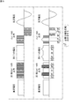
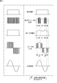
- FIG. 6 is a waveform diagram simply showing the characteristics of the operation of the DC / DC converter and the inverter in the minimum switching conversion method, and particularly, a diagram displayed so that the amplitude relationship from the DC input to the AC output is easy to see.
- FIG. 6 is a waveform diagram simply showing the characteristics of the operation of the DC / DC converter and the inverter in the minimum switching conversion method, and particularly, a diagram displayed so that the amplitude relationship from the DC input to the AC output is easy to see.
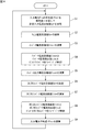
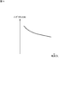
- FIG. 4 is a waveform diagram briefly showing the characteristics of the operation of the DC / DC converter and the inverter in the minimum switching conversion method, and particularly, a diagram displayed so that the timing of control is easy to see. It is a flowchart which shows the control process of a DC / DC converter and an inverter performed by a control part, when the power converter device is performing the power conversion from direct current to alternating current. It is a graph which shows an example of the characteristic of the inductance with respect to the electric current of a reactor. It is a wave form chart as an example which shows what happens to the output current of a power converter, when a reactor which can be selected practically and has a suitable direct current superposition characteristic is used.
- a full bridge inverter is configured by bridge-connecting four switching elements.
- the switching element of the upper arm and the switching element of the lower arm are connected in series with each other. Therefore, when the switching element of the upper arm and the switching element of the lower arm are turned on at the same time, the two wires are short-circuited. Therefore, the upper arm switching element and the lower arm switching element are controlled to be alternately turned on, and at the same time, the upper and lower switching elements are switched on / off so that the moment when the upper arm switching element and the lower arm switching element cannot be turned on simultaneously.
- a dead time is provided in which both the upper and lower switching elements are turned off.
- the gist of the embodiment of the present invention includes at least the following.
- This is a power conversion device that performs power conversion between direct current and alternating current, and includes a conversion unit configured by a switching element, an AC reactor connected to the AC side of the conversion unit, and the alternating current A current sensor that detects a current flowing through the reactor and a switching control of the switching element while performing feedback control of the AC current flowing through the AC reactor, and a gain characteristic with respect to an instantaneous value of the AC current is relatively small. And a control unit that changes the feedback gain so as to have a high gain with respect to the value and a low gain with respect to the large current value.
- the feedback gain is changed so that the gain is relatively high with respect to a small current value and the low gain with respect to a large current value.
- the followability of the feedback control can be enhanced with a relatively high gain.
- the stability of the feedback control can be ensured with a relatively low gain and oscillation can be prevented. In this manner, waveform distortion in the vicinity of the zero cross of the alternating current can be reliably suppressed.
- the gain characteristic may correspond to a DC superposition characteristic of current versus inductance in the AC reactor.
- the gain characteristic reflecting the direct current superimposition characteristic unique to the reactor can be obtained. That is, when the inductance of the AC reactor decreases due to an increase in current, the gain also decreases and stable control can be performed, and when the inductance of the AC reactor increases due to a decrease in current, the gain also increases and feedback is performed. The followability of control can be improved.
- the gain characteristic is such that, with respect to the phase of the AC current flowing through the AC reactor, the gain is higher as the peak value is closer to the maximum gain at the zero cross and away from the zero cross. It may decrease smoothly and become the minimum gain at the peak value. In this case, the gain smoothly changes so as to be the highest at the zero cross and the lowest at the peak value.
- the alternating current is a calculation target current value in the control unit.
- the gain characteristic is obtained based on the target current value, so that the stability of the feedback control can be obtained more reliably.
- the alternating current is a value detected by the current sensor. In this case, it is possible to obtain a gain characteristic that immediately corresponds to the actual detection value.
- a power conversion device comprising a DC / DC converter provided between the DC power supply and a DC bus, and connected to the DC bus and included in the voltage of the DC bus
- a small-capacity intermediate capacitor that does not smooth the pulsation twice the frequency of the AC voltage
- an inverter connected to the DC bus, the inverter and the AC circuit, the AC reactor
- a filter circuit including an AC side capacitor, wherein the DC / DC converter and the inverter constitute the conversion unit, and the control unit generates the AC voltage from the DC voltage.
- the DC voltage is boosted by the DC / DC converter, the inverter performs one of the non-inversion passage and the inversion passage of polarity, and the DC / DC converter is stopped.
- the DC / DC converter is stopped.
- it is a power converter device which controls so that the time which performs any one of a pressure
- the voltage is boosted by the DC / DC converter within one AC cycle, the inverter stops the high-frequency switching, the voltage is lowered by the inverter, and the DC / DC converter Control in which the timing for stopping switching alternately appears is performed.
- the waveform of the AC voltage to be generated is a composite waveform output by the DC / DC converter and the inverter operating alternately, and the DC / DC converter generates a waveform region having a relatively large absolute value before and after the peak value.
- the inverter generates a waveform region having a relatively small absolute value before and after the zero cross.
- the feedback gain is changed so that the gain is relatively high with respect to a small current value and low with respect to a large current value.
- the gain can be lowered to ensure the stability of the feedback control.
- this is a power that includes a conversion unit constituted by switching elements and an AC reactor connected to the AC side of the conversion unit, and performs power conversion between DC and AC.
- a current distortion reduction method executed by a control unit for the current flowing through the AC reactor, wherein the switching element is switched while feedback control of the AC current flowing through the AC reactor is performed, and the AC
- This is a current distortion reduction method in which the feedback gain is changed so that the gain characteristic with respect to the instantaneous current value is relatively high with respect to a small current value and low with respect to a large current value.
- the feedback gain is changed so as to have a relatively high gain for a small current value and a low gain for a large current value.
- the followability of the feedback control can be enhanced with a relatively high gain.
- the stability of the feedback control can be ensured with a relatively low gain, and oscillation can be prevented. In this way, waveform distortion in the vicinity of the zero cross of the alternating current can be suppressed.
- this power converter device can also be expressed as follows. That is, a power conversion device that performs power conversion between direct current and alternating current, a conversion unit configured by a switching element, an AC reactor connected to the AC side of the conversion unit, and a current flowing through the AC reactor And a control unit that performs switching control of the switching element while performing feedback control of the AC current flowing through the AC reactor, and the control unit is configured to perform DC superimposition of current versus inductance in the AC reactor.
- the gain characteristic with respect to the instantaneous value of the alternating current is relatively high with respect to the zero cross and the small current value in the vicinity thereof, the high gain, the peak value, and the vicinity thereof.
- the feedback gain is set so that the gain is relatively high with respect to the small current value and low with respect to the large current value within one cycle of the alternating current.
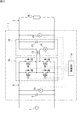
- FIG. 1 is a circuit diagram of a power conversion device according to a first example.
- the power converter is provided between a DC power source 2 and an AC circuit 3 which are, for example, photovoltaic power generation panels, and the DC voltage of the DC power source 2 is higher than the peak value (crest value) of the AC voltage of the AC circuit 3. Power conversion from direct current to alternating current can be performed in a high state.
- the AC power path 3 is connected to a consumer load 4L on which the power converter 1 is installed and a commercial power system 4P.
- the power conversion device 1 includes a DC-side capacitor 5, an inverter 10, and a filter circuit 11 as main circuit components.
- the inverter 10 connected to the DC bus 8 includes switching elements Q3 to Q6 that constitute a full bridge circuit.
- These switching elements Q3 to Q6 are, for example, MOSFETs (Metal-Oxide-Semiconductor Field Effect Transistors). In the case of a MOSFET, the switching elements Q3 to Q6 have diodes (body diodes) d3 to d6, respectively.
- the switching elements Q3 to Q6 are controlled by the control unit 14.
- a filter circuit 11 is provided between the inverter 10 and the AC circuit 3.
- the filter circuit 11 includes an AC reactor 12 and an AC side capacitor 13 provided on the load 4L side (right side in the figure) from the AC reactor 12.
- the filter circuit 11 prevents passage of high-frequency noise generated in the inverter 10 so as not to leak to the AC electric circuit 3 side.
- a voltage sensor 15 for detecting a DC side voltage is provided.
- the voltage sensor 15 is connected in parallel with the DC power source 2 and the DC side capacitor 5 and detects a DC voltage. Information on the detected voltage is provided to the control unit 14.
- a current sensor 18 for detecting a current flowing through the AC reactor 12 is provided on the AC side. Information on the current detected by the current sensor 18 is provided to the control unit 14. A voltage sensor 19 is provided in parallel with the AC capacitor 13. Information on the voltage detected by the voltage sensor 19 is provided to the control unit 14.
- the control unit 14 includes, for example, a computer, and a necessary control function is realized by the computer executing a software (computer program).
- the software is stored in a storage device (not shown) of the control unit 14.
- the control unit 14 controls the inverter so that the current flowing through the AC reactor 12 matches the target value. 10 is feedback controlled. Thereby, the inverter 10 performs a switching operation so as to output a current whose phase is synchronized with the voltage of the commercial power system 4P, and performs current control.
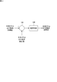
- FIG. 2 is a control block diagram of the feedback control executed by the control unit 14.
- the AC reactor output current target value and the AC reactor output current detection value are compared in the adding unit 143, and the difference is compared with the triangular wave as the output through the current control compensation unit 144 becomes the AC reactor output current reference wave.
- a PWM (Pulse Width Modulation) pulse for driving the inverter 10 is generated.
- FIG. 3 is a circuit diagram of the power conversion device according to the second example.
- a power conversion device 1 is provided between a DC power source 2 that is, for example, a photovoltaic power generation panel and an AC circuit 3, and the DC voltage of the DC power source 2 is a peak value (crest value) of the AC voltage of the AC circuit 3.
- a load 4 ⁇ / b> L of a consumer in which the power conversion device 1 is installed is connected to the AC circuit 3. That is, this is the power conversion device 1 that operates independently without being connected to the commercial power system.
- the circuit configuration in the power converter 1 is the same as that in FIG.
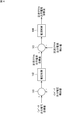
- FIG. 4 is a control block diagram of feedback control executed by the control unit 14 in the case of self-sustained operation.
- the inverter output voltage target value and the inverter output voltage detection value are compared in the adder 141, and the output of the difference passing through the voltage control compensator 142 becomes the AC reactor output current target value.
- the AC reactor output current target value and the AC reactor output current detection value are compared in the adder 143, and the difference between them is a triangular wave that is output through the current control compensator 144 as an AC reactor output current reference wave.
- a PWM pulse for driving the inverter 10 is generated.
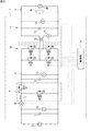
- FIG. 5 is an example of a circuit diagram of the power conversion device according to the third example.
- the power conversion device 1 is provided between a DC power source 2 and an AC circuit 3, and the DC voltage of the DC power source 2 is changed from the DC in a state where the DC voltage of the AC circuit 3 is lower than the peak value (crest value) of the AC voltage. Power conversion can be performed to AC or vice versa.
- the AC power path 3 is connected to a consumer load 4L on which the power converter 1 is installed and a commercial power system 4P.
- the power converter 1 includes a direct-current side capacitor 5, a DC / DC converter 6, an intermediate capacitor 9, an inverter 10, and a filter circuit 11 as main circuit components.
- the DC / DC converter 6 includes a DC reactor 7, a high-side switching element Q1, and a low-side switching element Q2, and constitutes a DC chopper circuit.
- the switching elements Q1 and Q2 for example, MOSFETs can be used.
- the MOSFET switching elements Q1, Q2 have diodes (body diodes) d1, d2, respectively. Each switching element Q1, Q2 is controlled by the control unit 14.
- the high voltage side of the DC / DC converter 6 is connected to the DC bus 8.
- the intermediate capacitor 9 connected between the two lines of the DC bus 8 has a small capacity (100 ⁇ F or less, for example, several tens of ⁇ F), and exhibits a smoothing action for a voltage switched at a high frequency (for example, 20 kHz). However, it does not exert a smoothing action on a voltage that changes at a frequency (100 Hz or 120 Hz) that is about twice the commercial frequency.
- the inverter 10 connected to the DC bus 8 includes switching elements Q3 to Q6 that constitute a full bridge circuit.
- These switching elements Q3 to Q6 are, for example, MOSFETs.
- the switching elements Q3 to Q6 have diodes (body diodes) d3 to d6, respectively.
- the switching elements Q3 to Q6 are controlled by the control unit 14.
- a filter circuit 11 is provided between the inverter 10 and the AC circuit 3.
- the filter circuit 11 includes an AC reactor 12 and an AC side capacitor 13 provided on the load 4L side (right side in the figure) from the AC reactor 12.
- the filter circuit 11 prevents passage of high-frequency noise generated in the inverter 10 so as not to leak to the AC electric circuit 3 side.
- a voltage sensor 15 and a current sensor 16 are provided on the low voltage side (left side in the figure) of the DC / DC converter 6.
- the voltage sensor 15 is connected in parallel with the DC power supply 2 and detects the voltage across the DC power supply 2. Information on the detected voltage is provided to the control unit 14.
- the current sensor 16 detects a current flowing through the DC / DC converter 6. Information on the detected current is provided to the control unit 14.
- a voltage sensor 17 is connected in parallel to the intermediate capacitor 9. The voltage sensor 17 detects the voltage across the intermediate capacitor 9, that is, the voltage of the DC bus 8. Information on the detected voltage is provided to the control unit 14.
- a current sensor 18 for detecting a current flowing through the AC reactor 12 is provided on the AC side. Information on the current detected by the current sensor 18 is provided to the control unit 14. A voltage sensor 19 is provided in parallel with the AC capacitor 13. Information on the voltage detected by the voltage sensor 19 is provided to the control unit 14.
- the control unit 14 includes, for example, a computer, and a necessary control function is realized by the computer executing a software (computer program).
- the software is stored in a storage device (not shown) of the control unit 14.
- FIG. 6 and 7 are waveform diagrams simply showing the characteristics of the operation of the DC / DC converter 6 and the inverter 10 in the minimum switching conversion method. Although both figures show the same contents, FIG. 6 shows the amplitude relationship from the DC input to the AC output in an easy-to-see manner, and FIG. 7 shows the control timing in an easy-to-see manner.
- the upper part of FIG. 6 and the left column of FIG. 7 are waveform diagrams representing traditional switching control that is not the minimum switching conversion method, for comparison.
- the lower part of FIG. 6 and the right column of FIG. 7 are waveform diagrams showing the operation of the minimum switching conversion method.
- the output at the interconnection point of the pair of switching elements of the DC / DC converter and the DC reactor with respect to the input DC voltage is It is in the form of an equidistant pulse train having a value higher than the DC voltage.
- This output is smoothed by an intermediate capacitor and appears as a voltage on the DC bus.
- the inverter performs PWM-controlled switching while inverting the polarity in a half cycle. As a result, a sinusoidal AC voltage is obtained through final smoothing.
- the absolute value of the instantaneous value of the AC voltage (hereinafter simply referred to as the absolute value of the AC voltage) and the input DC voltage
- the DC / DC converter 6 and the inverter 10 operate according to the comparison result. Specifically, when the absolute value of the AC voltage is smaller than (or below) the DC voltage, the DC / DC converter 6 stops (“ST” in the figure), and the absolute value of the AC voltage is equal to or greater than the DC voltage. When (or larger), the DC / DC converter 6 performs a boosting operation (“OP” in the figure). The output of the DC / DC converter 6 is smoothed by the intermediate capacitor 9 and appears on the DC bus 8 as the illustrated voltage.
- the intermediate capacitor 9 has a small capacity, a part of the waveform around the peak of the absolute value of the AC voltage remains without being smoothed. That is, the smoothing works to the extent that the trace of the high frequency switching by the DC / DC converter 6 is erased, but the intermediate capacitor 9 has a small capacity so that the low frequency about twice the commercial frequency cannot be smoothed. It has become.
- the inverter 10 performs high-frequency switching when the absolute value of the AC voltage is smaller than (or less than) the DC voltage according to the comparison result between the absolute value of the AC voltage and the DC voltage (see FIG.
- the high frequency switching is stopped (“ST” in the figure).
- the inverter 10 has the switching elements Q3 and Q6 on, Q4 and Q5 off (non-inverted), the switching elements Q3 and Q6 off, and Q4 and Q5 on ( By selecting one of (inversion), only necessary polarity inversion is performed.
- the output of the inverter 10 is smoothed by the AC reactor 12 and the AC side capacitor 13, and a desired AC output is obtained.
- the DC / DC converter 6 and the inverter 10 are alternately performing high-frequency switching operation, and when the DC / DC converter 6 is performing a boosting operation, The inverter 10 stops high-frequency switching and performs only necessary polarity inversion with respect to the voltage of the DC bus 8. Conversely, when the inverter 10 performs high-frequency switching operation, the DC / DC converter 6 stops and the voltage across the DC-side capacitor 5 appears on the DC bus 8 via the DC reactor 7 and the diode d1.
- Such a power conversion device 1 can reduce the overall number of high-frequency switching operations by generating a pause in the high-frequency switching of the switching elements Q1 to Q6. Thereby, the efficiency of power conversion can be improved significantly.
- FIG. 8 is a flowchart showing a control process of the DC / DC converter 6 and the inverter 10 executed by the control unit 14 when the power conversion device 1 performs power conversion from direct current to alternating current.
- the control unit 14 calculates the current input power average value ⁇ Pin>.
- the symbol ⁇ > is used to mean an average value (the same applies hereinafter).
- the input power average value ⁇ Pin> is obtained based on the following formula (1).
- ⁇ Pin> ⁇ Iin ⁇ Vg> (1)
- Iin is a DC / DC converter current detection value detected by the current sensor 16.
- Vg is a DC input voltage detection value detected by the voltage sensor 15.
- control unit 14 sets the DC input current target value Ig * as compared with the input power average value ⁇ Pin> at the previous calculation (step S1).
- instantaneous values that are not averaged are used for the current detection value Iin and the DC input voltage detection value Vg.
- control part 14 calculates the average value ⁇ Ia *> of the output current target value as the power converter device 1 based on following formula (2).
- ⁇ Ia *> ⁇ ⁇ Ig * ⁇ Vg> / ⁇ Va> (2)
- ⁇ is a constant representing the conversion efficiency of the power conversion device 1.
- Va is a system voltage detection value detected by the voltage sensor 19.
- the control unit 14 calculates an inverter current target value Iinv * (current target value on the AC side of the inverter 10), which is a current target value for controlling the inverter 10, according to the following equation (4) (step) S3).
- Iinv * Ia * + s CaVa (4)
- Ca is the capacitance of the AC side capacitor 13
- s is a Laplace operator (the same applies hereinafter).
- the second term on the right side in the equation (4) is a value added in consideration of the current flowing through the AC capacitor 13 of the filter circuit 11.
- the control unit 14 performs feedback control of the inverter 10 based on the inverter current target value Iinv * and the actual inverter current detection value Iinv detected by the current sensor 18 (step S4).
- the control unit 14 calculates the inverter output voltage target value Vinv * (voltage target value on the AC side of the inverter 10) based on the following equation (5) (step S5).
- Vinv * Va + ZaIinv * (5)
- Za is the impedance of the AC reactor 12.
- the second term on the right side of Equation (5) is a value added in consideration of the voltage generated at both ends of the AC reactor 12.
- control unit 14 is an inverter current target value that is a current target value for controlling the inverter 10 so that the current phase of the AC power output from the power converter 1 is in phase with the system voltage detection value Va. Based on Iinv *, an inverter output voltage target value Vinv * is set.
- the control unit 14 compares the voltage Vg as the voltage on the DC power supply side or preferably the following DC voltage Vgf with the absolute value of the inverter output voltage target value Vinv *. Then, the larger one is determined as the DC / DC converter voltage target value Vo * (step S6).
- control unit 14 calculates a DC / DC converter current target value Iin * based on the following equation (7) (step S7).
- Iin * ⁇ (Iinv * ⁇ Vinv *) + (s C Vo *) ⁇ Vo * ⁇ / (Vg-ZIin) (7)
- C is the capacitance of the intermediate capacitor 9.
- Equation (7) the second term added to the product of the inverter current target value Iinv * and the inverter output voltage target value Vinv * is a value that takes into account reactive power passing through the intermediate capacitor 9. That is, the value of Iin * can be obtained more accurately by considering reactive power in addition to the power target value of the inverter 10. Furthermore, if the power loss of the power converter 1 is measured in advance, the power loss can also be considered as the second term plus the third term in the equation (7).
- Iin * (Iinv * ⁇ Vinv *) / Vg (8)
- Iin * obtained by this equation (8) can be used as Iin included in the right side of equations (6) and (7).
- the DC / DC converter 6 is feedback controlled by this DC / DC converter current target value Iin *.
- the DC / DC converter 6 is feedback-controlled by the DC / DC converter current target value Iin * and the DC / DC converter current detection value Iin (step S8).
- step S8 the control unit 14 obtains the current input power average value ⁇ Pin> based on the above-described equation (1) (step S9).
- the control unit 14 feedback-controls the inverter 10 and the DC / DC converter 6 with the current target value.
- the feedback control in step S4 is performed based on the inverter current target value Iinv * and the inverter current detection value Iinv.
- the feedback control in step S8 is performed based on the DC / DC converter current target value Iin * and the DC / DC converter current detection value Iin.
- the DC / DC converter current target value Iin * is based on the inverter current target value Iinv * (Equation (7), Equation (8)). Therefore, both feedback controls are based on the inverter current target value Iinv *.
- G (constant) is an ideal gain related to control of the current flowing through the AC reactor 12
- L constant is the inductance of the AC reactor 12
- f constant is the control frequency. ing.
- G L ⁇ f (9)
- the inductance of the reactor (not limited to AC and DC) is not a constant.
- the reactor has a DC superposition characteristic, and has a characteristic that the inductance decreases as the flowing current increases. If the reactor does not exhibit such characteristics remarkably, the change in L in equation (9) is small, and therefore the gain can be easily set.
- such a reactor with a small change in inductance is very expensive.
- FIG. 9 is a graph showing an example of the characteristics of the inductance of the reactor with respect to the current. As illustrated, the inductance decreases as the current increases. If the current further increases excessively, the inductance is lost due to magnetic saturation, and a large current flows, but it is assumed that the current is used in a current range in which such magnetic saturation does not occur.
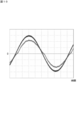
- FIG. 10 is a waveform diagram as an example showing what happens to the output current of the power converter when a reactor that can be actually selected and has a corresponding DC superimposition characteristic is used.
- the waveform with the larger amplitude is the voltage waveform
- the waveform with the smaller amplitude is the waveform of the output current output through the AC reactor.
- the waveform of the output current is distorted near the zero cross.
- the third harmonic component becomes large and exceeds the distortion reference value required by the standard.
- the closer to the absolute peak value the smaller the distortion. Therefore, it is conceivable to change the gain within one cycle of the output current.
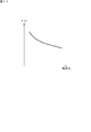
- FIG. 11 is an example of a graph showing change characteristics when the gain is changed with respect to the current.
- this is a characteristic corresponding to the DC superposition characteristic. That is, the larger the current, the smaller the gain. The smaller the current, the greater the gain.
- Feedback control is performed to apply such gain characteristics to a target value or detection value of an output current that is alternating current. That is, the control unit 14 changes the feedback gain so that the gain characteristic with respect to the instantaneous value of the alternating current is relatively high gain for the small current value and low gain for the large current value.
- FIG. 12 is a diagram showing an example of a specific function for obtaining the change characteristics as shown in FIG.
- the proportional coefficient in the P control (proportional control) of the feedback control is set to the maximum value of 10.
- the proportionality coefficient is set to the minimum value of 6.5. Then, between 0 and ( ⁇ / 2), it is smoothly reduced to 10 to 6.5. Between ( ⁇ / 2) and ⁇ , it is increased smoothly to 6.5 to 10. Between ⁇ and (3 ⁇ / 2), it is reduced smoothly to 10 to 6.5. Then, between (3 ⁇ / 2) and 2 ⁇ , it is smoothly increased to 6.5 to 10.
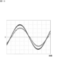
- FIG. 13 is a waveform diagram in the case where the above-described current-gain characteristics are applied to the AC reactor used in FIG.
- the waveform with the larger amplitude is the voltage waveform
- the waveform with the smaller amplitude is the waveform of the output current output through the AC reactor.
- the distortion at zero crossing is improved. Specifically, the following numerical values were obtained in comparison with FIG.
- the basics of the feedback control are such that the gain characteristic with respect to the instantaneous value of the alternating current flowing through the AC reactor 12 is relatively high gain with respect to a small current value and low gain with respect to a large current value.
- the feedback gain is changed so that Thereby, in the vicinity of the zero cross (small current value) of the waveform of the alternating current flowing through the alternating current reactor 12, the follow-up performance of the feedback control can be enhanced with a relatively high gain. Further, in the vicinity of the peak value (large current value) of the waveform of the alternating current, the stability of the feedback control can be ensured with a relatively low gain, and oscillation can be prevented. In this manner, waveform distortion in the vicinity of the zero cross of the alternating current can be reliably suppressed.
- the gain characteristics correspond to the DC superposition characteristics of current versus inductance in the AC reactor 12.
- the gain characteristic reflecting the direct current superimposition characteristic unique to the reactor can be obtained. That is, when the inductance of the AC reactor 12 is decreased due to an increase in current, the gain is also decreased and stable control can be performed. When the inductance of the AC reactor 12 is increased due to a decrease in current, the gain is also increased. The follow-up performance of feedback control can be improved.
- the gain characteristic is preferably such that the phase of the alternating current flowing through the AC reactor 12 is the highest gain at the zero cross, the gain decreases more smoothly as the peak value moves away from the zero cross, and becomes the lowest gain at the peak value. . In this case, the gain smoothly changes so as to be the highest at the zero cross and the lowest at the peak value.
- the alternating current is a current target value calculated in the control unit 14, gain characteristics are obtained based on the current target value, so that the stability of the feedback control can be obtained more reliably.
- the alternating current is a detection value obtained by a current sensor, a gain characteristic corresponding to the actual detection value can be obtained.
- the feedback gain by changing the feedback gain so that a relatively high gain is obtained for a small current value and a low gain relation for a large current value is applied to feedback control of the output current in the minimum switching method.
- the gain can be lowered to ensure the stability of the feedback control.
- the power conversion devices 1 of the first to third examples are merely examples. Changing the feedback gain so that it is relatively high gain for a small current value and low gain for a large current value is a variety of power conversions that have a converter that outputs via an AC reactor. It can be applied to the device.
Landscapes
- Engineering & Computer Science (AREA)
- Power Engineering (AREA)
- Inverter Devices (AREA)
- Dc-Dc Converters (AREA)
Abstract
直流と交流との間で電力変換を行う電力変換装置であって、スイッチング素子によって構成される変換部と、変換部の交流側に接続された交流リアクトルと、交流リアクトルに流れる電流を検出する電流センサと、交流リアクトルに流す交流電流のフィードバック制御を行いつつスイッチング素子のスイッチング制御を行い、交流電流の瞬時値に対するゲイン特性が、相対的に、小電流値に対して高ゲイン、大電流値に対して低ゲインの関係となるようにフィードバックゲインを変化させる制御部と、を備えている電力変換装置である。
Description
本発明は、電力変換装置及び電流歪の低減方法に関する。
本出願は、2016年10月4日出願の日本出願第2016-196146号に基づく優先権を主張し、前記日本出願に記載された全ての記載内容を援用するものである。
本出願は、2016年10月4日出願の日本出願第2016-196146号に基づく優先権を主張し、前記日本出願に記載された全ての記載内容を援用するものである。
直流を交流に変換して商用電力系統と系統連系する電力変換装置には、インバータが搭載されている。インバータは、MOSFET(Metal-Oxide-Semiconductor Field Effect Transistor)、IGBT(Insulated Gate Bipolar Transistor)等のスイッチング素子によって構成され、スイッチング素子は高周波スイッチング動作を行う。インバータの出力は、コンデンサ及び交流リアクトルを含むフィルタ回路を通して、商用電力系統へ提供される。
系統連系する電力変換装置のインバータは、商用電力系統と連系動作するために、商用電力系統の交流電圧と同期した正弦波状の電流を目標値として動作する。目標値に沿って出力するために、インバータを制御する制御部は、インバータから商用電力系統への出力電流を検出して、スイッチング素子のオン・オフ時間を制御するフィードバック制御を行っている。
また、系統連系する以上、電力の品質が求められる。例えば、出力電流の波形に含まれる歪が、所定の歪率以下であることが必要とされる。歪を低減するための一案として、例えば、出力電流の波形のゼロクロス付近では、それ以外の位相の時よりも、スイッチング周波数を高くするという制御方法が提案されている(例えば、特許文献1参照。)。スイッチング周波数の高周波化によって制御周波数も高周波化すると、フィードバック制御を、より短時間のサイクルで行える。これによりフィードバック制御の追従性を向上させることができると期待される。
なお、系統連系せず、自立運転のみを行う電力変換装置であっても、同様にフィードバック制御の追従性を向上させて出力電圧の歪を低減する方が好ましい。
一表現としての本発明は、直流と交流との間で電力変換を行う電力変換装置であって、スイッチング素子によって構成される変換部と、前記変換部の交流側に接続された交流リアクトルと、前記交流リアクトルに流れる電流を検出する電流センサと、前記交流リアクトルに流す交流電流のフィードバック制御を行いつつ前記スイッチング素子のスイッチング制御を行い、前記交流電流の瞬時値に対するゲイン特性が、相対的に、小電流値に対して高ゲイン、大電流値に対して低ゲインの関係となるようにフィードバックゲインを変化させる制御部と、を備えている電力変換装置である。
他の表現としての本発明は、スイッチング素子によって構成される変換部、及び、前記変換部の交流側に接続された交流リアクトルを備え、直流と交流との間で電力変換を行う電力変換装置において、前記交流リアクトルに流れる電流について制御部によって実行される電流歪の低減方法であって、前記交流リアクトルに流す交流電流のフィードバック制御を行いつつ前記スイッチング素子のスイッチング制御を行い、前記交流電流の瞬時値に対するゲイン特性が、相対的に、小電流値に対して高ゲイン、大電流値に対して低ゲインの関係となるようにフィードバックゲインを変化させる、電流歪の低減方法である。
[本開示が解決しようとする課題]
例えばフルブリッジインバータは、4個のスイッチング素子がブリッジ接続されて構成されている。直流電圧が印加される2線間にある1つのレグは、上アームのスイッチング素子と、下アームのスイッチング素子とが、互いに直列接続されている。従って、上アームのスイッチング素子と、下アームのスイッチング素子とが互いに同時にオンになると、上記2線間を短絡することになってしまう。そこで、上アームのスイッチング素子及び下アームのスイッチング素子は必ず交互にオンするよう制御し、しかも、同時にオン状態である瞬間ができないよう、上下のスイッチング素子がオン/オフを交代する時間帯に、上下のスイッチング素子が共にオフとなるデッドタイムを設ける。
例えばフルブリッジインバータは、4個のスイッチング素子がブリッジ接続されて構成されている。直流電圧が印加される2線間にある1つのレグは、上アームのスイッチング素子と、下アームのスイッチング素子とが、互いに直列接続されている。従って、上アームのスイッチング素子と、下アームのスイッチング素子とが互いに同時にオンになると、上記2線間を短絡することになってしまう。そこで、上アームのスイッチング素子及び下アームのスイッチング素子は必ず交互にオンするよう制御し、しかも、同時にオン状態である瞬間ができないよう、上下のスイッチング素子がオン/オフを交代する時間帯に、上下のスイッチング素子が共にオフとなるデッドタイムを設ける。
しかしながら、前述のようにスイッチング周波数を局所的に高める電力変換装置では、高周波化によって、制御の1周期が短くなる中でデッドタイムを確保しなければならない。その結果、制御周期に占めるデッドタイムの時間割合が増える。このため、理想の出力制御との誤差が大きくなり、狙い通りに歪が低減できるとは限らなくなる。
かかる従来の問題点に鑑み、本開示は、電力変換装置において、より確実性のある歪の低減を実現することを目的とする。
[本開示の効果]
本開示によれば、電力変換装置において、より確実性のある歪の低減を実現することができる。
本開示によれば、電力変換装置において、より確実性のある歪の低減を実現することができる。
[実施形態の要旨]
本発明の実施形態の要旨としては、少なくとも以下のものが含まれる。
本発明の実施形態の要旨としては、少なくとも以下のものが含まれる。
(1)これは、直流と交流との間で電力変換を行う電力変換装置であって、スイッチング素子によって構成される変換部と、前記変換部の交流側に接続された交流リアクトルと、前記交流リアクトルに流れる電流を検出する電流センサと、前記交流リアクトルに流す交流電流のフィードバック制御を行いつつ前記スイッチング素子のスイッチング制御を行い、前記交流電流の瞬時値に対するゲイン特性が、相対的に、小電流値に対して高ゲイン、大電流値に対して低ゲインの関係となるようにフィードバックゲインを変化させる制御部と、を備えている電力変換装置である。
上記のように構成された電力変換装置では、相対的に、小電流値に対して高ゲイン、大電流値に対して低ゲインの関係となるようにフィードバックゲインを変化させることにより、交流リアクトルを通して流れる交流電流の波形のゼロクロス近傍(小電流値)では相対的に高ゲインでフィードバック制御の追従性を高めることができる。また、交流電流の波形のピーク値近傍(大電流値)では相対的に低ゲインでフィードバック制御の安定性を確保し、発振を防止することができる。このようにして、交流電流のゼロクロス近傍での波形の歪を確実に抑制することができる。
(2)また、(1)の電力変換装置において、前記ゲイン特性は、前記交流リアクトルにおける電流対インダクタンスの直流重畳特性に対応したものであってもよい。
この場合、リアクトル固有の直流重畳特性を反映したゲイン特性とすることができる。すなわち、相対的に、交流リアクトルのインダクタンスが電流の増大により低下するとゲインも低下して、安定した制御を行うことができ、交流リアクトルのインダクタンスが電流の減少により上昇するとゲインも上昇して、フィードバック制御の追従性を高めることができる。
この場合、リアクトル固有の直流重畳特性を反映したゲイン特性とすることができる。すなわち、相対的に、交流リアクトルのインダクタンスが電流の増大により低下するとゲインも低下して、安定した制御を行うことができ、交流リアクトルのインダクタンスが電流の減少により上昇するとゲインも上昇して、フィードバック制御の追従性を高めることができる。
(3)また、(1)又は(2)の電力変換装置において、前記ゲイン特性は、前記交流リアクトルに流れる交流電流の位相に関して、ゼロクロスで最高ゲイン、ゼロクロスから離れてピーク値に近いほどゲインが滑らかに低下し、ピーク値で最低ゲインとなるものであってもよい。
この場合、ゲインは、ゼロクロスで最高となり、ピーク値で最低となるように滑らかに変化する。
この場合、ゲインは、ゼロクロスで最高となり、ピーク値で最低となるように滑らかに変化する。
(4)また、(1)~(3)のいずれかの電力変換装置において、例えば、前記交流電流とは、前記制御部における演算上の電流目標値である。
この場合、電流目標値に基づいてゲイン特性が得られるので、フィードバック制御の安定性を、より確実に得ることができる。
この場合、電流目標値に基づいてゲイン特性が得られるので、フィードバック制御の安定性を、より確実に得ることができる。
(5)また、(1)~(3)のいずれかの電力変換装置において、例えば、前記交流電流とは、前記電流センサによる検出値である。
この場合、実際の検出値に即応したゲイン特性を得ることができる。
この場合、実際の検出値に即応したゲイン特性を得ることができる。
(6)また、これは、直流電源と交流電路との間に設けられ、前記直流電源の直流電圧が前記交流電路の交流電圧のピーク値より低い状態で直流/交流の電力変換を行う、(1)~(5)のいずれかの電力変換装置であって、前記直流電源とDCバスとの間に設けられたDC/DCコンバータと、前記DCバスに接続され、前記DCバスの電圧に含まれる前記交流電圧の周波数の2倍の脈動を平滑しない程度の小容量の中間コンデンサと、前記DCバスに接続されたインバータと、前記インバータと前記交流電路との間に設けられ、前記交流リアクトル及び交流側コンデンサを含むフィルタ回路と、を備え、前記DC/DCコンバータ及び前記インバータが、前記変換部を構成し、前記制御部は、前記直流電圧から前記交流電圧を生成するにあたって、交流1サイクル内で、前記DC/DCコンバータにより前記直流電圧を昇圧し、前記インバータは極性の非反転通過及び反転通過のいずれか一方を行う時期、及び、前記DC/DCコンバータを停止して、前記インバータにより降圧並びに、極性の非反転通過及び反転通過のいずれか一方を行う時期が、交互に出現するよう制御する、電力変換装置である。
上記(6)のような電力変換装置では基本的に、交流1サイクル内で、DC/DCコンバータによって昇圧し、インバータは高周波スイッチングを停止する時期と、インバータによって降圧し、DC/DCコンバータは高周波スイッチングを停止する時期とが交互に現れる制御が行われている。いわば、生成する交流電圧の波形は、DC/DCコンバータとインバータとが交互に動作して出力する合成波形であり、ピーク値前後の絶対値が相対的に大きい波形領域はDC/DCコンバータが生成し、ゼロクロス前後の絶対値が相対的に小さい波形領域はインバータが生成する。このような、最小スイッチング変換方式における出力電流のフィードバック制御に対して、相対的に、小電流値に対して高ゲイン、大電流値に対して低ゲインの関係となるようにフィードバックゲインを変化させることにより、交流1サイクル中のゼロクロス近傍でのスイッチングを担当するインバータによる歪を低減することができる。また、交流1サイクル中の瞬時値の絶対値におけるピーク値近傍でのスイッチングを担当するDC/DCコンバータに対しては、ゲインを下げ、フィードバック制御の安定性を確保することができる。
(7)他の観点からは、これは、スイッチング素子によって構成される変換部、及び、前記変換部の交流側に接続された交流リアクトルを備え、直流と交流との間で電力変換を行う電力変換装置において、前記交流リアクトルに流れる電流について制御部によって実行される電流歪の低減方法であって、前記交流リアクトルに流す交流電流のフィードバック制御を行いつつ前記スイッチング素子のスイッチング制御を行い、前記交流電流の瞬時値に対するゲイン特性が、相対的に、小電流値に対して高ゲイン、大電流値に対して低ゲインの関係となるようにフィードバックゲインを変化させる、電流歪の低減方法である。
上記のような電流歪の低減方法においては、相対的に、小電流値に対して高ゲイン、大電流値に対して低ゲインの関係となるようにフィードバックゲインを変化させることにより、交流リアクトルを通して流れる交流電流の波形のゼロクロス近傍(小電流値)では相対的に高ゲインでフィードバック制御の追従性を高めることができる。また、交流電流の波形のピーク値近傍(大電流値)では相対的に低ゲインでフィードバック制御の安定性を確保し、発振を防止することができる。このようにして、交流電流のゼロクロス近傍での波形の歪を抑制することができる。
(8)また、この電力変換装置は、以下のように表現することもできる。
すなわち、直流と交流との間で電力変換を行う電力変換装置であって、スイッチング素子によって構成される変換部と、前記変換部の交流側に接続された交流リアクトルと、前記交流リアクトルに流れる電流を検出する電流センサと、前記交流リアクトルに流す交流電流のフィードバック制御を行いつつ前記スイッチング素子のスイッチング制御を行う制御部と、を備え、前記制御部は、前記交流リアクトルにおける電流対インダクタンスの直流重畳特性に対応して、前記交流電流の1周期内で、前記交流電流の瞬時値に対するゲイン特性が、相対的に、ゼロクロス及びその近傍の小電流値に対して高ゲイン、ピーク値及びその近傍の大電流値に対して低ゲインの関係となるようにフィードバックゲインを変化させる、電力変換装置である。
すなわち、直流と交流との間で電力変換を行う電力変換装置であって、スイッチング素子によって構成される変換部と、前記変換部の交流側に接続された交流リアクトルと、前記交流リアクトルに流れる電流を検出する電流センサと、前記交流リアクトルに流す交流電流のフィードバック制御を行いつつ前記スイッチング素子のスイッチング制御を行う制御部と、を備え、前記制御部は、前記交流リアクトルにおける電流対インダクタンスの直流重畳特性に対応して、前記交流電流の1周期内で、前記交流電流の瞬時値に対するゲイン特性が、相対的に、ゼロクロス及びその近傍の小電流値に対して高ゲイン、ピーク値及びその近傍の大電流値に対して低ゲインの関係となるようにフィードバックゲインを変化させる、電力変換装置である。
上記のように構成された電力変換装置では、交流電流の1周期内で、相対的に、小電流値に対して高ゲイン、大電流値に対して低ゲインの関係となるようにフィードバックゲインを変化させることにより、交流リアクトルを通して流れる交流電流の波形のゼロクロス近傍(小電流値)では相対的に高ゲインでフィードバック制御の追従性を高めることができる。また、交流電流の波形のピーク値近傍(大電流値)では相対的に低ゲインでフィードバック制御の安定性を確保し、発振を防止することができる。このようにして、交流電流のゼロクロス近傍での波形の歪を確実に抑制することができる。
[実施形態の詳細]
以下、本発明の実施形態に係る電力変換装置について、図面を参照して説明する。
以下、本発明の実施形態に係る電力変換装置について、図面を参照して説明する。
《回路構成_第1例》
図1は、第1例に係る電力変換装置の回路図である。図において、電力変換装置は、例えば太陽光発電パネルである直流電源2と交流電路3との間に設けられ、直流電源2の直流電圧が交流電路3の交流電圧のピーク値(波高値)より高い状態で、直流から交流へ電力変換を行うことができる。交流電路3には、電力変換装置1が設置されている需要家の負荷4L、及び、商用電力系統4Pが接続されている。
図1は、第1例に係る電力変換装置の回路図である。図において、電力変換装置は、例えば太陽光発電パネルである直流電源2と交流電路3との間に設けられ、直流電源2の直流電圧が交流電路3の交流電圧のピーク値(波高値)より高い状態で、直流から交流へ電力変換を行うことができる。交流電路3には、電力変換装置1が設置されている需要家の負荷4L、及び、商用電力系統4Pが接続されている。
電力変換装置1は、主回路構成要素として、直流側コンデンサ5、インバータ10、及び、フィルタ回路11を備えている。
DCバス8に接続されたインバータ10は、フルブリッジ回路を構成するスイッチング素子Q3~Q6を備えている。これらスイッチング素子Q3~Q6は、例えば、MOSFET(Metal-Oxide-Semiconductor Field Effect Transistor)である。MOSFETの場合は、スイッチング素子Q3~Q6がそれぞれ、ダイオード(ボディダイオード)d3~d6を有している。各スイッチング素子Q3~Q6は、制御部14により制御される。
DCバス8に接続されたインバータ10は、フルブリッジ回路を構成するスイッチング素子Q3~Q6を備えている。これらスイッチング素子Q3~Q6は、例えば、MOSFET(Metal-Oxide-Semiconductor Field Effect Transistor)である。MOSFETの場合は、スイッチング素子Q3~Q6がそれぞれ、ダイオード(ボディダイオード)d3~d6を有している。各スイッチング素子Q3~Q6は、制御部14により制御される。
インバータ10と交流電路3との間には、フィルタ回路11が設けられている。フィルタ回路11は、交流リアクトル12と、交流リアクトル12より負荷4L側(図の右側)に設けられた交流側コンデンサ13とを備えている。フィルタ回路11は、インバータ10で発生する高周波ノイズが交流電路3側へ漏れ出ないように、通過を阻止している。
計測用の回路要素としては、直流側の電圧を検出する電圧センサ15が設けられている。電圧センサ15は直流電源2及び直流側コンデンサ5と並列接続され、直流電圧を検出する。検出された電圧の情報は、制御部14に提供される。
一方、交流側には、交流リアクトル12に流れる電流を検出する電流センサ18が設けられている。電流センサ18によって検出された電流の情報は、制御部14に提供される。また、交流側コンデンサ13と並列に、電圧センサ19が設けられている。電圧センサ19によって検出された電圧の情報は、制御部14に提供される。
制御部14は例えば、コンピュータを含み、ソフトウェア(コンピュータプログラム)をコンピュータが実行することで、必要な制御機能を実現する。ソフトウェアは、制御部14の記憶装置(図示せず。)に格納される。
上記のように商用電力系統4Pと連系する電力変換装置1では、出力電圧の波形は商用電力系統4Pにより決まるので、制御部14は、交流リアクトル12に流れる電流が目標値に一致するようインバータ10をフィードバック制御する。これによりインバータ10は、商用電力系統4Pの電圧と位相が同期した電流を出力するようにスイッチング動作し、電流制御を行う。
図2は、制御部14によって実行される、上記フィードバック制御の制御ブロック図である。交流リアクトル出力電流目標値と、交流リアクトル出力電流検出値とは、加算部143において比較され、その差が電流制御の補償部144を通った出力が交流リアクトル出力電流参照波となって三角波と比較され、インバータ10を駆動するPWM(Pulse Width Modulation)パルスが生成される。
《回路構成_第2例》
図3は、第2例に係る電力変換装置の回路図である。図において、電力変換装置1は、例えば太陽光発電パネルである直流電源2と、交流電路3との間に設けられ、直流電源2の直流電圧が交流電路3の交流電圧のピーク値(波高値)より高い状態で、直流から交流へ電力変換を行うことができる。交流電路3には、電力変換装置1が設置されている需要家の負荷4Lが接続される。すなわち、これは、商用電力系統とは接続されずに、自立運転する電力変換装置1である。電力変換装置1内の回路構成は図1と同様である。
図3は、第2例に係る電力変換装置の回路図である。図において、電力変換装置1は、例えば太陽光発電パネルである直流電源2と、交流電路3との間に設けられ、直流電源2の直流電圧が交流電路3の交流電圧のピーク値(波高値)より高い状態で、直流から交流へ電力変換を行うことができる。交流電路3には、電力変換装置1が設置されている需要家の負荷4Lが接続される。すなわち、これは、商用電力系統とは接続されずに、自立運転する電力変換装置1である。電力変換装置1内の回路構成は図1と同様である。
自立運転する電力変換装置1では、制御部14は、電圧制御及び電流制御を行う。
図4は、制御部14によって実行される、自立運転の場合のフィードバック制御の制御ブロック図である。
図4において、インバータ出力電圧目標値と、インバータ出力電圧検出値とは、加算部141において比較され、その差が電圧制御の補償部142を通った出力が交流リアクトル出力電流目標値となる。そして、交流リアクトル出力電流目標値と、交流リアクトル出力電流検出値とは、加算部143において比較され、その差が電流制御の補償部144を通った出力が交流リアクトル出力電流参照波となって三角波と比較され、インバータ10を駆動するPWMパルスが生成される。
図4は、制御部14によって実行される、自立運転の場合のフィードバック制御の制御ブロック図である。
図4において、インバータ出力電圧目標値と、インバータ出力電圧検出値とは、加算部141において比較され、その差が電圧制御の補償部142を通った出力が交流リアクトル出力電流目標値となる。そして、交流リアクトル出力電流目標値と、交流リアクトル出力電流検出値とは、加算部143において比較され、その差が電流制御の補償部144を通った出力が交流リアクトル出力電流参照波となって三角波と比較され、インバータ10を駆動するPWMパルスが生成される。
《回路構成例_第3例》
次に、さらに複雑な制御の例について説明する。
図5は、第3例に係る電力変換装置の回路図の一例である。図において、電力変換装置1は、直流電源2と交流電路3との間に設けられ、直流電源2の直流電圧が交流電路3の交流電圧のピーク値(波高値)より低い状態で、直流から交流へ、又は必要によりその逆に、電力変換を行うことができる。交流電路3には、電力変換装置1が設置されている需要家の負荷4L、及び、商用電力系統4Pが接続されている。
次に、さらに複雑な制御の例について説明する。
図5は、第3例に係る電力変換装置の回路図の一例である。図において、電力変換装置1は、直流電源2と交流電路3との間に設けられ、直流電源2の直流電圧が交流電路3の交流電圧のピーク値(波高値)より低い状態で、直流から交流へ、又は必要によりその逆に、電力変換を行うことができる。交流電路3には、電力変換装置1が設置されている需要家の負荷4L、及び、商用電力系統4Pが接続されている。
電力変換装置1は、主回路構成要素として、直流側コンデンサ5、DC/DCコンバータ6、中間コンデンサ9、インバータ10、及び、フィルタ回路11を備えている。DC/DCコンバータ6は、直流リアクトル7と、ハイサイドのスイッチング素子Q1と、ローサイドのスイッチング素子Q2とを備え、直流チョッパ回路を構成している。スイッチング素子Q1,Q2としては例えば、MOSFETを使用することができる。MOSFETのスイッチング素子Q1,Q2はそれぞれ、ダイオード(ボディダイオード)d1,d2を有している。各スイッチング素子Q1,Q2は、制御部14により制御される。
DC/DCコンバータ6の高圧側は、DCバス8に接続されている。DCバス8の2線間に接続されている中間コンデンサ9は、小容量(100μF以下、例えば数十μF)であり、高周波(例えば20kHz)でスイッチングされた電圧に対しては平滑作用を発揮するが、商用周波数の2倍程度の周波数(100Hz又は120Hz)で変化する電圧に対しては平滑作用を発揮しない。
DCバス8に接続されたインバータ10は、フルブリッジ回路を構成するスイッチング素子Q3~Q6を備えている。これらスイッチング素子Q3~Q6は、例えば、MOSFETである。MOSFETの場合は、スイッチング素子Q3~Q6がそれぞれ、ダイオード(ボディダイオード)d3~d6を有している。各スイッチング素子Q3~Q6は、制御部14により制御される。
インバータ10と交流電路3との間には、フィルタ回路11が設けられている。フィルタ回路11は、交流リアクトル12と、交流リアクトル12より負荷4L側(図の右側)に設けられた交流側コンデンサ13とを備えている。フィルタ回路11は、インバータ10で発生する高周波ノイズが交流電路3側へ漏れ出ないように、通過を阻止している。
計測用の回路要素としては、DC/DCコンバータ6の低圧側(図の左側)に、電圧センサ15及び電流センサ16が設けられている。電圧センサ15は直流電源2と並列接続され、直流電源2の両端電圧を検出する。検出された電圧の情報は、制御部14に提供される。電流センサ16は、DC/DCコンバータ6に流れる電流を検出する。検出された電流の情報は、制御部14に提供される。中間コンデンサ9には電圧センサ17が並列接続されている。電圧センサ17は、中間コンデンサ9の両端電圧すなわち、DCバス8の電圧を検出する。検出された電圧の情報は、制御部14に提供される。
一方、交流側には、交流リアクトル12に流れる電流を検出する電流センサ18が設けられている。電流センサ18によって検出された電流の情報は、制御部14に提供される。また、交流側コンデンサ13と並列に、電圧センサ19が設けられている。電圧センサ19によって検出された電圧の情報は、制御部14に提供される。
制御部14は例えば、コンピュータを含み、ソフトウェア(コンピュータプログラム)をコンピュータが実行することで、必要な制御機能を実現する。ソフトウェアは、制御部14の記憶装置(図示せず。)に格納される。
《電圧波形で見た最小スイッチング変換方式の概要》
次に、上記第3例に係る電力変換装置1において実行される最小スイッチング方式の動作について、その概要を説明する。
図6及び図7は、最小スイッチング変換方式における、DC/DCコンバータ6及びインバータ10の動作の特徴を簡略に示す波形図である。両図は同じ内容を示しているが、図6は特に、直流入力から交流出力までの振幅の関係が見やすいように表示し、図7は特に、制御のタイミングが見やすいように表示している。図6の上段及び図7の左欄はそれぞれ、比較のために、最小スイッチング変換方式ではない伝統的なスイッチング制御を表す波形図である。また、図6の下段及び図7の右欄はそれぞれ、最小スイッチング変換方式の動作を示す波形図である。
次に、上記第3例に係る電力変換装置1において実行される最小スイッチング方式の動作について、その概要を説明する。
図6及び図7は、最小スイッチング変換方式における、DC/DCコンバータ6及びインバータ10の動作の特徴を簡略に示す波形図である。両図は同じ内容を示しているが、図6は特に、直流入力から交流出力までの振幅の関係が見やすいように表示し、図7は特に、制御のタイミングが見やすいように表示している。図6の上段及び図7の左欄はそれぞれ、比較のために、最小スイッチング変換方式ではない伝統的なスイッチング制御を表す波形図である。また、図6の下段及び図7の右欄はそれぞれ、最小スイッチング変換方式の動作を示す波形図である。
まず、図6の上段(又は図7の左欄)において、伝統的なスイッチング制御では、入力される直流電圧に対する、DC/DCコンバータの一対のスイッチング素子及び直流リアクトルの相互接続点での出力は、直流電圧よりも高い値の等間隔のパルス列状である。この出力は中間コンデンサによって平滑化され、DCバスの電圧として現れる。これに対してインバータは、PWM制御されたスイッチングを半周期で極性反転しながら行う。この結果、最終的な平滑化を経て、正弦波の交流電圧が得られる。
次に、図6の下段(又は図7の右欄)の最小スイッチング変換方式では、交流電圧の瞬時値の絶対値(以下、単に交流電圧の絶対値という。)と、入力である直流電圧との比較結果に応じて、DC/DCコンバータ6とインバータ10とが動作する。具体的には、交流電圧の絶対値が直流電圧より小さいとき(又は以下のとき)は、DC/DCコンバータ6は停止し(図中の「ST」)、交流電圧の絶対値が直流電圧以上のとき(又は、より大きいとき)は、DC/DCコンバータ6が昇圧動作を行う(図中の「OP」)。DC/DCコンバータ6の出力は中間コンデンサ9により平滑化され、DCバス8に、図示の電圧として現れる。
ここで、中間コンデンサ9が小容量であることにより、交流電圧の絶対値のピーク前後となる一部の波形が平滑化されずにそのまま残る。すなわち、平滑は、DC/DCコンバータ6による高周波のスイッチングの痕跡を消す程度には作用するが、商用周波数の2倍程度の低周波を平滑化することはできないように、中間コンデンサ9が小容量になっている。
これに対してインバータ10は、交流電圧の絶対値と、直流電圧との比較結果に応じて、交流電圧の絶対値が直流電圧より小さいとき(又は以下のとき)は、高周波スイッチングを行い(図中の「OP」)、交流電圧の絶対値が直流電圧以上のとき(又は、より大きいとき)は、高周波スイッチングを停止する(図中の「ST」)。高周波スイッチングを停止しているときのインバータ10は、スイッチング素子Q3,Q6がオン、Q4,Q5がオフの状態(非反転)と、スイッチング素子Q3,Q6がオフ、Q4,Q5がオンの状態(反転)のいずれかを選択することにより、必要な極性反転のみを行う。インバータ10の出力は交流リアクトル12及び交流側コンデンサ13により平滑化され、所望の交流出力が得られる。
ここで、図7の右欄に示すように、DC/DCコンバータ6とインバータ10とは、交互に高周波スイッチングの動作をしており、DC/DCコンバータ6が昇圧の動作をしているときは、インバータ10は高周波スイッチングを停止し、DCバス8の電圧に対して必要な極性反転のみを行っている。逆に、インバータ10が高周波スイッチング動作するときは、DC/DCコンバータ6は停止して、直流側コンデンサ5の両端電圧が、直流リアクトル7及びダイオードd1を介してDCバス8に現れる。
以上のようにして、DC/DCコンバータ6とインバータ10とによる最小スイッチング変換方式の動作が行われる。このような電力変換装置1は、スイッチング素子Q1~Q6の高周波スイッチングに休止期間が生じることによって、全体的な高周波スイッチング回数を減らすことができる。これにより、電力変換の効率を、大幅に改善することができる。
《最小スイッチング変換方式の詳細》
図8は、電力変換装置1が直流から交流への電力変換を行っている場合に、制御部14によって実行される、DC/DCコンバータ6及びインバータ10の制御処理を示すフローチャートである。
図8は、電力変換装置1が直流から交流への電力変換を行っている場合に、制御部14によって実行される、DC/DCコンバータ6及びインバータ10の制御処理を示すフローチャートである。
まず、エンドレスな処理ループのステップS9から見ると、制御部14は、現状の入力電力平均値〈Pin〉を演算する。なお、この記号〈 〉は平均値を意味するものとして用いる(以下同様。)。入力電力平均値〈Pin〉は、下記式(1)に基づいて求められる。
〈Pin〉=〈Iin×Vg〉 ・・・(1)
ここで、Iinは、電流センサ16によって検出されるDC/DCコンバータ電流検出値である。また、Vgは、電圧センサ15によって検出される直流入力電圧検出値である。
〈Pin〉=〈Iin×Vg〉 ・・・(1)
ここで、Iinは、電流センサ16によって検出されるDC/DCコンバータ電流検出値である。また、Vgは、電圧センサ15によって検出される直流入力電圧検出値である。
次に、制御部14は、前回演算時の入力電力平均値〈Pin〉と比較して、直流入力電流目標値Ig*を設定する(ステップS1)。
なお、式(1)以外の以下に示す制御に関する各式においては、電流検出値Iin、及び直流入力電圧検出値Vgは、平均化されていない瞬時値が用いられる。
なお、式(1)以外の以下に示す制御に関する各式においては、電流検出値Iin、及び直流入力電圧検出値Vgは、平均化されていない瞬時値が用いられる。
続いて制御部14は、下記式(2)に基づいて、電力変換装置1としての出力電流目標値の平均値〈Ia*〉を演算する。
〈Ia*〉=η〈Ig*×Vg〉/〈Va〉 ・・・(2)
ここで、ηは電力変換装置1の変換効率を表す定数である。Vaは、電圧センサ19によって検出される、系統電圧検出値である。
〈Ia*〉=η〈Ig*×Vg〉/〈Va〉 ・・・(2)
ここで、ηは電力変換装置1の変換効率を表す定数である。Vaは、電圧センサ19によって検出される、系統電圧検出値である。
さらに、制御部14は、下記式(3)に基づいて、出力電流目標値Ia*を、系統電圧検出値Vaと同位相の正弦波として求める(ステップS2)。すなわち制御部14は、電力変換装置1が出力する交流電力の電流Ia(出力電流)が系統電圧(系統電圧検出値Va)と同位相となるようにインバータ10を制御する。
Ia*=(√2)×〈Ia*〉×sinωt ・・・(3)
このようにして、制御部14は、入力電力平均値〈Pin〉及び系統電圧検出値Vaに基づいて出力電流目標値Ia*を求める。
Ia*=(√2)×〈Ia*〉×sinωt ・・・(3)
このようにして、制御部14は、入力電力平均値〈Pin〉及び系統電圧検出値Vaに基づいて出力電流目標値Ia*を求める。
次に、制御部14は、下記式(4)により、インバータ10を制御するための電流目標値であるインバータ電流目標値Iinv*(インバータ10の交流側での電流目標値)を演算する(ステップS3)。
Iinv*=Ia* + s CaVa ・・・(4)
ここで、Caは、交流側コンデンサ13の静電容量、sはラプラス演算子である(以下同様。)。式(4)中の右辺第2項は、フィルタ回路11の交流側コンデンサ13に流れる電流を考慮して加算した値である。
Iinv*=Ia* + s CaVa ・・・(4)
ここで、Caは、交流側コンデンサ13の静電容量、sはラプラス演算子である(以下同様。)。式(4)中の右辺第2項は、フィルタ回路11の交流側コンデンサ13に流れる電流を考慮して加算した値である。
制御部14は、インバータ電流目標値Iinv*と、電流センサ18によって検出される実際のインバータ電流検出値Iinvとに基づいて、インバータ10をフィードバック制御する(ステップS4)。
一方、制御部14は、下記式(5)に基づいて、インバータ出力電圧目標値Vinv*(インバータ10の交流側での電圧目標値)を演算する(ステップS5)。
Vinv*=Va+ZaIinv* ・・・(5)
ここで、Zaは、交流リアクトル12のインピーダンスである。
式(5)の右辺第2項は、交流リアクトル12の両端に発生する電圧を考慮して加算した値である。
Vinv*=Va+ZaIinv* ・・・(5)
ここで、Zaは、交流リアクトル12のインピーダンスである。
式(5)の右辺第2項は、交流リアクトル12の両端に発生する電圧を考慮して加算した値である。
このように、制御部14は、電力変換装置1が出力する交流電力の電流位相が系統電圧検出値Vaと同位相となるようにインバータ10を制御するための電流目標値であるインバータ電流目標値Iinv*に基づいて、インバータ出力電圧目標値Vinv*を設定する。
次に、制御部14は、下記式(6)に示すように、直流電源側の電圧としての電圧Vg又は好ましくは下記の直流電圧Vgfと、インバータ出力電圧目標値Vinv*の絶対値とを比較して、大きい方をDC/DCコンバータ電圧目標値Vo*に決定する(ステップS6)。
直流電圧Vgfとは、Vgに直流リアクトル7のインピーダンスZによる電圧降下を考慮した電圧であり、DC/DCコンバータ電流検出値をIinとして、Vgf=Vg-ZIinである。従って、
Vo*=Max(Vg-ZIin,|Vinv*|) ・・・(6)
とすることができる。
直流電圧Vgfとは、Vgに直流リアクトル7のインピーダンスZによる電圧降下を考慮した電圧であり、DC/DCコンバータ電流検出値をIinとして、Vgf=Vg-ZIinである。従って、
Vo*=Max(Vg-ZIin,|Vinv*|) ・・・(6)
とすることができる。
さらに、制御部14は、下記式(7)に基づいて、DC/DCコンバータ電流目標値Iin*を演算する(ステップS7)。
Iin*={(Iinv*×Vinv*) +(s C Vo*)×Vo*}
/(Vg-ZIin) ・・・(7)
ここで、Cは、中間コンデンサ9の静電容量である。
Iin*={(Iinv*×Vinv*) +(s C Vo*)×Vo*}
/(Vg-ZIin) ・・・(7)
ここで、Cは、中間コンデンサ9の静電容量である。
式(7)中、インバータ電流目標値Iinv*と、インバータ出力電圧目標値Vinv*との積に加算されている第2項は、中間コンデンサ9を通過する無効電力を考慮した値である。すなわち、インバータ10の電力目標値に加えて、無効電力を考慮することにより、より正確にIin*の値を求めることができる。なお、さらに、予め電力変換装置1の電力損失を測定しておけば、式(7)の上記第2項プラス第3項として、電力損失も考慮することができる。
なお、中間コンデンサ9の静電容量C及び電力損失が、(Iinv*×Vinv*)に比べて十分小さい場合、下記式(8)が成立する。
Iin*=(Iinv*×Vinv*)/Vg ・・・(8)
この式(8)によって求まるIin*を、式(6)、(7)の右辺に含まれるIinとして用いることができる。
DC/DCコンバータ6は、このDC/DCコンバータ電流目標値Iin*によって、フィードバック制御される。
Iin*=(Iinv*×Vinv*)/Vg ・・・(8)
この式(8)によって求まるIin*を、式(6)、(7)の右辺に含まれるIinとして用いることができる。
DC/DCコンバータ6は、このDC/DCコンバータ電流目標値Iin*によって、フィードバック制御される。
以上のようにして、DC/DCコンバータ6は、DC/DCコンバータ電流目標値Iin*と、DC/DCコンバータ電流検出値Iinとによって、フィードバック制御される(ステップS8)。
上記ステップS8の後、制御部14は、前述の式(1)に基づいて、現状の入力電力平均値〈Pin〉を求める(ステップS9)。
制御部14は、上述したように、インバータ10及びDC/DCコンバータ6を電流目標値によってフィードバック制御する。
ステップS4のフィードバック制御は、インバータ電流目標値Iinv*と、インバータ電流検出値Iinvに基づいて行われる。
ステップS8のフィードバック制御は、DC/DCコンバータ電流目標値Iin*と、DC/DCコンバータ電流検出値Iinとに基づいて行われる。ここで、DC/DCコンバータ電流目標値Iin*は、インバータ電流目標値Iinv*に基づいている(式(7)、式(8))。
従って、どちらのフィードバック制御も、インバータ電流目標値Iinv*に基づいている。
ステップS4のフィードバック制御は、インバータ電流目標値Iinv*と、インバータ電流検出値Iinvに基づいて行われる。
ステップS8のフィードバック制御は、DC/DCコンバータ電流目標値Iin*と、DC/DCコンバータ電流検出値Iinとに基づいて行われる。ここで、DC/DCコンバータ電流目標値Iin*は、インバータ電流目標値Iinv*に基づいている(式(7)、式(8))。
従って、どちらのフィードバック制御も、インバータ電流目標値Iinv*に基づいている。
《第1例~第3例におけるフィードバック制御に共通する課題》
以上のように、電力変換装置1の回路構成の第1例~第3例を挙げたが、いずれも、交流リアクトル12の電流制御(インバータ電流制御)が基本になっている。電流制御は一般的なフィードバック制御と同様に、ゲイン(比例係数)を大きくすると目標値への追従性は良くなるが、発振するなどの、不安定動作に至りやすい。逆に、ゲインが小さいと、安定性は良くなるが目標値への追随性が低下する。目標値に対する追随性の低下は出力電流の波形の歪につながる。
以上のように、電力変換装置1の回路構成の第1例~第3例を挙げたが、いずれも、交流リアクトル12の電流制御(インバータ電流制御)が基本になっている。電流制御は一般的なフィードバック制御と同様に、ゲイン(比例係数)を大きくすると目標値への追従性は良くなるが、発振するなどの、不安定動作に至りやすい。逆に、ゲインが小さいと、安定性は良くなるが目標値への追随性が低下する。目標値に対する追随性の低下は出力電流の波形の歪につながる。
交流リアクトル12に流れる電流制御に関する理想的なゲインをG(定数)、交流リアクトル12のインダクタンスをL(定数)、制御周波数をf(定数)とすると、一般に、以下の関係にあることが知られている。
G=L・f ・・・(9)
G=L・f ・・・(9)
しかしながら、実際には、リアクトル(交流用、直流用に限らず。)のインダクタンスは定数ではない。リアクトルには、直流重畳特性があり、流れる電流が大きくなるほど、インダクタンスが小さくなる特性がある。このような特性が顕著に表れないリアクトルであれば、式(9)におけるLの変化が小さく、従って、ゲインの設定もし易い。しかし、そのようにインダクタンスの変化が少ないリアクトルは、とても高価である。現実的に選択し得る製品としては、磁気飽和さえしなければ、インダクタンスの変化があっても、安価なリアクトルを使用したいところである。
図9は、リアクトルの、電流に対するインダクタンスの特性の一例を示すグラフである。図示のように、電流が増大するほど、インダクタンスは低下する。なお、さらに過度に電流が増大すると、磁気飽和によりインダクタンスが失われ、大電流が流れるが、そのような磁気飽和は起こらない電流範囲で使用することを前提としている。
図10は、現実的に選択し得るリアクトルであって、相応の直流重畳特性を有するものを使用した場合に、電力変換装置の出力電流がどうなるかを示す一例としての波形図である。図において、振幅の大きい方の波形は電圧波形であり、振幅の小さい方の波形が、交流リアクトルを通して出力される出力電流の波形である。
図10より、出力電流の波形は、ゼロクロス近傍で歪を生じている。この場合、第3次高調波成分が大きくなり、規格で求められる歪の基準値を超える。
一方、ゼロクロス近傍を除く領域では、絶対値でのピーク値に近いほど、歪は少ない。
そこで、ゲインを出力電流の1周期内で変化させることが考えられる。
一方、ゼロクロス近傍を除く領域では、絶対値でのピーク値に近いほど、歪は少ない。
そこで、ゲインを出力電流の1周期内で変化させることが考えられる。
図11は、電流に対してゲインを変化させる場合の、変化特性を示すグラフの一例である。図9との比較により明らかなように、これは、直流重畳特性に対応した特性である。すなわち、電流が大きいほど、ゲインは小さい。電流が小さいほど、ゲインは大きい。このようなゲイン特性を交流である出力電流の目標値又は検出値に適用するフィードバック制御を行う。すなわち、制御部14は、交流電流の瞬時値に対するゲイン特性が、相対的に、小電流値に対して高ゲイン、大電流値に対して低ゲインの関係となるようにフィードバックゲインを変化させる。
図12は、図11のような変化特性を得るための具体的な関数の一例を示す図である。図12において、ゼロクロスである位相[rad]0、π、2πでは、フィードバック制御のP制御(比例制御)における比例係数を最大値の10とする。また、瞬時値の絶対値でピーク値となる位相[rad](π/2)、(3π/2)では、比例係数を最小値の6.5とする。そして、0~(π/2)の間では、10~6.5へ滑らかに減少させる。(π/2)~πの間では、6.5~10へ滑らかに増大させる。π~(3π/2)の間では、10~6.5へ滑らかに減少させる。そして、(3π/2)~2πの間では、6.5~10へ滑らかに増大させる。
図13は、図10で用いた交流リアクトルに、上記のような電流対ゲインの特性を適用した場合の波形図である。図13において、振幅の大きい方の波形は電圧波形であり、振幅の小さい方の波形が、交流リアクトルを通して出力される出力電流の波形である。ゼロクロスでの歪は改善されている。具体的には、図10との比較において以下のような数値が得られた。
<図10>
総合歪率:4.1%
3次高調波:3.1%
5次高調波:1.7%
7次高調波:1.1%
総合歪率:4.1%
3次高調波:3.1%
5次高調波:1.7%
7次高調波:1.1%
<図13>
総合歪率:2.4%
3次高調波:1.3%
5次高調波:1.0%
7次高調波:0.67%
総合歪率:2.4%
3次高調波:1.3%
5次高調波:1.0%
7次高調波:0.67%
上記比較により明らかなように、総合歪率及び各次高調波の全てにおいて3%未満となる顕著な改善効果が得られた。
《まとめ》
以上のように、このフィードバック制御の基本は、交流リアクトル12に流す交流電流の瞬時値に対するゲイン特性が、相対的に、小電流値に対して高ゲイン、大電流値に対して低ゲインの関係となるようにフィードバックゲインを変化させることである。これにより、交流リアクトル12を通して流れる交流電流の波形のゼロクロス近傍(小電流値)では相対的に高ゲインでフィードバック制御の追従性を高めることができる。また、交流電流の波形のピーク値近傍(大電流値)では相対的に低ゲインでフィードバック制御の安定性を確保し、発振を防止することができる。このようにして、交流電流のゼロクロス近傍での波形の歪を確実に抑制することができる。
以上のように、このフィードバック制御の基本は、交流リアクトル12に流す交流電流の瞬時値に対するゲイン特性が、相対的に、小電流値に対して高ゲイン、大電流値に対して低ゲインの関係となるようにフィードバックゲインを変化させることである。これにより、交流リアクトル12を通して流れる交流電流の波形のゼロクロス近傍(小電流値)では相対的に高ゲインでフィードバック制御の追従性を高めることができる。また、交流電流の波形のピーク値近傍(大電流値)では相対的に低ゲインでフィードバック制御の安定性を確保し、発振を防止することができる。このようにして、交流電流のゼロクロス近傍での波形の歪を確実に抑制することができる。
また、ゲイン特性は、交流リアクトル12における電流対インダクタンスの直流重畳特性に対応したものである。この場合、リアクトル固有の直流重畳特性を反映したゲイン特性とすることができる。すなわち、相対的に、交流リアクトル12のインダクタンスが電流の増大により低下するとゲインも低下して、安定した制御を行うことができ、交流リアクトル12のインダクタンスが電流の減少により上昇するとゲインも上昇して、フィードバック制御の追従性を高めることができる。
また、ゲイン特性は好ましくは、交流リアクトル12に流れる交流電流の位相に関して、ゼロクロスで最高ゲイン、ゼロクロスから離れてピーク値に近いほどゲインが滑らかに低下し、ピーク値で最低ゲインとなるものである。この場合、ゲインは、ゼロクロスで最高となり、ピーク値で最低となるように滑らかに変化する。
また、交流電流が、制御部14における演算上の電流目標値である場合には、電流目標値に基づいてゲイン特性が得られるので、フィードバック制御の安定性を、より確実に得ることができる。
逆に、交流電流が、電流センサによる検出値である場合には、実際の検出値に即応したゲイン特性を得ることができる。
逆に、交流電流が、電流センサによる検出値である場合には、実際の検出値に即応したゲイン特性を得ることができる。
また、相対的に、小電流値に対して高ゲイン、大電流値に対して低ゲインの関係となるようにフィードバックゲインを変化させることを最小スイッチング方式における出力電流のフィードバック制御に適用することで、交流1サイクル中のゼロクロス近傍でのスイッチングを担当するインバータ10による歪を低減することができる。また、交流1サイクル中の瞬時値の絶対値におけるピーク値近傍でのスイッチングを担当するDC/DCコンバータ6に対しては、ゲインを下げ、フィードバック制御の安定性を確保することができる。
《補記》
なお、第1例~第3例の電力変換装置1は、例示に過ぎない。相対的に、小電流値に対して高ゲイン、大電流値に対して低ゲインの関係となるようにフィードバックゲインを変化させることは、交流リアクトルを介して出力する変換部を有する各種の電力変換装置に適用することができる。
なお、第1例~第3例の電力変換装置1は、例示に過ぎない。相対的に、小電流値に対して高ゲイン、大電流値に対して低ゲインの関係となるようにフィードバックゲインを変化させることは、交流リアクトルを介して出力する変換部を有する各種の電力変換装置に適用することができる。
なお、今回開示された実施の形態はすべての点で例示であって制限的なものではないと考えられるべきである。本発明の範囲は請求の範囲によって示され、請求の範囲と均等の意味及び範囲内での全ての変更が含まれることが意図される。
1 電力変換装置
2 直流電源
3 交流電路
4L 負荷
4P 商用電力系統
5 直流側コンデンサ
6 DC/DCコンバータ
7 直流リアクトル
8 DCバス
9 中間コンデンサ
10 インバータ
11 フィルタ回路
12 交流リアクトル
13 交流側コンデンサ
14 制御部
15 電圧センサ
16 電流センサ
17 電圧センサ
18 電流センサ
19 電圧センサ
141 加算部
142 補償部
143 加算部
144 補償部
d1~d6 ダイオード
Q1~Q6 スイッチング素子
2 直流電源
3 交流電路
4L 負荷
4P 商用電力系統
5 直流側コンデンサ
6 DC/DCコンバータ
7 直流リアクトル
8 DCバス
9 中間コンデンサ
10 インバータ
11 フィルタ回路
12 交流リアクトル
13 交流側コンデンサ
14 制御部
15 電圧センサ
16 電流センサ
17 電圧センサ
18 電流センサ
19 電圧センサ
141 加算部
142 補償部
143 加算部
144 補償部
d1~d6 ダイオード
Q1~Q6 スイッチング素子
Claims (8)
- 直流と交流との間で電力変換を行う電力変換装置であって、
スイッチング素子によって構成される変換部と、
前記変換部の交流側に接続された交流リアクトルと、
前記交流リアクトルに流れる電流を検出する電流センサと、
前記交流リアクトルに流す交流電流のフィードバック制御を行いつつ前記スイッチング素子のスイッチング制御を行い、前記交流電流の瞬時値に対するゲイン特性が、相対的に、小電流値に対して高ゲイン、大電流値に対して低ゲインの関係となるようにフィードバックゲインを変化させる制御部と、
を備えている電力変換装置。 - 前記ゲイン特性は、前記交流リアクトルにおける電流対インダクタンスの直流重畳特性に対応したものである請求項1に記載の電力変換装置。
- 前記ゲイン特性は、前記交流リアクトルに流れる交流電流の位相に関して、ゼロクロスで最高ゲイン、ゼロクロスから離れてピーク値に近いほどゲインが滑らかに低下し、ピーク値で最低ゲインとなるものである請求項1又は請求項2に記載の電力変換装置。
- 前記交流電流とは、前記制御部における演算上の電流目標値である請求項1~請求項3に記載の電力変換装置。
- 前記交流電流とは、前記電流センサによる検出値である請求項1~請求項3に記載の電力変換装置。
- 直流電源と交流電路との間に設けられ、前記直流電源の直流電圧が前記交流電路の交流電圧のピーク値より低い状態で直流/交流の電力変換を行う、請求項1~請求項5のいずれか1項に記載の電力変換装置であって、
前記直流電源とDCバスとの間に設けられたDC/DCコンバータと、
前記DCバスに接続され、前記DCバスの電圧に含まれる前記交流電圧の周波数の2倍の脈動を平滑しない程度の小容量の中間コンデンサと、
前記DCバスに接続されたインバータと、
前記インバータと前記交流電路との間に設けられ、前記交流リアクトル及び交流側コンデンサを含むフィルタ回路と、を備え、
前記DC/DCコンバータ及び前記インバータが、前記変換部を構成し、
前記制御部は、前記直流電圧から前記交流電圧を生成するにあたって、交流1サイクル内で、前記DC/DCコンバータにより前記直流電圧を昇圧し、前記インバータは極性の非反転通過及び反転通過のいずれか一方を行う時期、及び、前記DC/DCコンバータを停止して、前記インバータにより降圧並びに、極性の非反転通過及び反転通過のいずれか一方を行う時期が、交互に出現するよう制御する、電力変換装置。 - スイッチング素子によって構成される変換部、及び、前記変換部の交流側に接続された交流リアクトルを備え、直流と交流との間で電力変換を行う電力変換装置において、前記交流リアクトルに流れる電流について制御部によって実行される電流歪の低減方法であって、
前記交流リアクトルに流す交流電流のフィードバック制御を行いつつ前記スイッチング素子のスイッチング制御を行い、前記交流電流の瞬時値に対するゲイン特性が、相対的に、小電流値に対して高ゲイン、大電流値に対して低ゲインの関係となるようにフィードバックゲインを変化させる、
電流歪の低減方法。 - 直流と交流との間で電力変換を行う電力変換装置であって、
スイッチング素子によって構成される変換部と、
前記変換部の交流側に接続された交流リアクトルと、
前記交流リアクトルに流れる電流を検出する電流センサと、
前記交流リアクトルに流す交流電流のフィードバック制御を行いつつ前記スイッチング素子のスイッチング制御を行う制御部と、を備え、
前記制御部は、前記交流リアクトルにおける電流対インダクタンスの直流重畳特性に対応して、前記交流電流の1周期内で、前記交流電流の瞬時値に対するゲイン特性が、相対的に、ゼロクロス及びその近傍の小電流値に対して高ゲイン、ピーク値及びその近傍の大電流値に対して低ゲインの関係となるようにフィードバックゲインを変化させる、電力変換装置。
Priority Applications (1)
| Application Number | Priority Date | Filing Date | Title |
|---|---|---|---|
| JP2018543586A JP6825627B2 (ja) | 2016-10-04 | 2017-06-13 | 電力変換装置及び電流歪の低減方法 |
Applications Claiming Priority (2)
| Application Number | Priority Date | Filing Date | Title |
|---|---|---|---|
| JP2016196146 | 2016-10-04 | ||
| JP2016-196146 | 2016-10-04 |
Publications (1)
| Publication Number | Publication Date |
|---|---|
| WO2018066176A1 true WO2018066176A1 (ja) | 2018-04-12 |
Family
ID=61830936
Family Applications (1)
| Application Number | Title | Priority Date | Filing Date |
|---|---|---|---|
| PCT/JP2017/021713 Ceased WO2018066176A1 (ja) | 2016-10-04 | 2017-06-13 | 電力変換装置及び電流歪の低減方法 |
Country Status (2)
| Country | Link |
|---|---|
| JP (1) | JP6825627B2 (ja) |
| WO (1) | WO2018066176A1 (ja) |
Cited By (3)
| Publication number | Priority date | Publication date | Assignee | Title |
|---|---|---|---|---|
| JP2019213366A (ja) * | 2018-06-06 | 2019-12-12 | 住友電気工業株式会社 | 電力変換装置、太陽光発電システム、及び、電力変換装置の制御方法 |
| CN112166549A (zh) * | 2018-05-29 | 2021-01-01 | 株式会社电装 | 电力转换装置的控制装置 |
| JPWO2022138215A1 (ja) * | 2020-12-21 | 2022-06-30 |
Citations (4)
| Publication number | Priority date | Publication date | Assignee | Title |
|---|---|---|---|---|
| JPS4872627A (ja) * | 1971-12-24 | 1973-10-01 | ||
| JP2005210862A (ja) * | 2004-01-26 | 2005-08-04 | Toyota Industries Corp | 電力変換装置 |
| JP2016010258A (ja) * | 2014-06-25 | 2016-01-18 | 株式会社日本自動車部品総合研究所 | 電力変換装置 |
| WO2016139990A1 (ja) * | 2015-03-05 | 2016-09-09 | 住友電気工業株式会社 | 変換装置 |
Family Cites Families (2)
| Publication number | Priority date | Publication date | Assignee | Title |
|---|---|---|---|---|
| JPH0638537A (ja) * | 1992-07-13 | 1994-02-10 | Nippon Electric Ind Co Ltd | 可変ゲイン適応制御機能を備えたpwmインバータ |
| JP2013059224A (ja) * | 2011-09-09 | 2013-03-28 | Panasonic Corp | 燃料電池の電力変換装置 |
-
2017
- 2017-06-13 WO PCT/JP2017/021713 patent/WO2018066176A1/ja not_active Ceased
- 2017-06-13 JP JP2018543586A patent/JP6825627B2/ja active Active
Patent Citations (4)
| Publication number | Priority date | Publication date | Assignee | Title |
|---|---|---|---|---|
| JPS4872627A (ja) * | 1971-12-24 | 1973-10-01 | ||
| JP2005210862A (ja) * | 2004-01-26 | 2005-08-04 | Toyota Industries Corp | 電力変換装置 |
| JP2016010258A (ja) * | 2014-06-25 | 2016-01-18 | 株式会社日本自動車部品総合研究所 | 電力変換装置 |
| WO2016139990A1 (ja) * | 2015-03-05 | 2016-09-09 | 住友電気工業株式会社 | 変換装置 |
Cited By (6)
| Publication number | Priority date | Publication date | Assignee | Title |
|---|---|---|---|---|
| CN112166549A (zh) * | 2018-05-29 | 2021-01-01 | 株式会社电装 | 电力转换装置的控制装置 |
| CN112166549B (zh) * | 2018-05-29 | 2023-12-12 | 株式会社电装 | 电力转换装置的控制装置 |
| JP2019213366A (ja) * | 2018-06-06 | 2019-12-12 | 住友電気工業株式会社 | 電力変換装置、太陽光発電システム、及び、電力変換装置の制御方法 |
| JPWO2022138215A1 (ja) * | 2020-12-21 | 2022-06-30 | ||
| JP7597127B2 (ja) | 2020-12-21 | 2024-12-10 | 株式会社村田製作所 | スイッチング電源装置 |
| US12368373B2 (en) | 2020-12-21 | 2025-07-22 | Murata Manufacturing Co., Ltd. | Switching power supply device |
Also Published As
| Publication number | Publication date |
|---|---|
| JP6825627B2 (ja) | 2021-02-03 |
| JPWO2018066176A1 (ja) | 2019-07-18 |
Similar Documents
| Publication | Publication Date | Title |
|---|---|---|
| JP5618022B1 (ja) | インバータ装置 | |
| CN101174794B (zh) | 电源电路及其中使用的控制电路 | |
| JP6327106B2 (ja) | 変換装置 | |
| TWI442681B (zh) | Power factor correction circuit for estimating input current and its control method | |
| JP6414546B2 (ja) | インバータ装置 | |
| JP5304937B2 (ja) | 電力変換装置 | |
| EP2528221A2 (en) | Multi-phase active rectifier | |
| WO2015105081A1 (ja) | 電力変換装置及び三相交流電源装置 | |
| WO2016006273A1 (ja) | 電力変換装置及び三相交流電源装置 | |
| JP6414491B2 (ja) | 変換装置 | |
| JP2016082786A (ja) | 中性点クランプ形電力変換装置およびその制御方法 | |
| JP6354623B2 (ja) | 変換装置 | |
| CN105940597A (zh) | 电力变换装置的控制方法 | |
| US10348190B2 (en) | Conversion device for converting voltage in a non-insulated manner and method for controlling the same | |
| JP6399239B2 (ja) | 電力変換装置 | |
| JP6825627B2 (ja) | 電力変換装置及び電流歪の低減方法 | |
| JP2011239564A (ja) | 中性点クランプ式電力変換装置 | |
| JP6750508B2 (ja) | 電力変換装置及びその高調波抑制方法 | |
| WO2017068814A1 (ja) | 電力変換装置及びその制御方法 | |
| JP2011193583A (ja) | 3レベル電力変換装置 | |
| JP2018183035A (ja) | 電力変換装置及びその制御方法 | |
| JP6874773B2 (ja) | 電力変換装置及びその制御方法 | |
| JP4517762B2 (ja) | スイッチング制御方法、整流装置及び駆動システム | |
| JP6946799B2 (ja) | 電源システム | |
| JPWO2024257406A5 (ja) |
Legal Events
| Date | Code | Title | Description |
|---|---|---|---|
| 121 | Ep: the epo has been informed by wipo that ep was designated in this application |
Ref document number: 17858016 Country of ref document: EP Kind code of ref document: A1 |
|
| ENP | Entry into the national phase |
Ref document number: 2018543586 Country of ref document: JP Kind code of ref document: A |
|
| NENP | Non-entry into the national phase |
Ref country code: DE |
|
| 122 | Ep: pct application non-entry in european phase |
Ref document number: 17858016 Country of ref document: EP Kind code of ref document: A1 |