WO2018043077A1 - モータ駆動制御装置およびモータ駆動制御方法 - Google Patents
モータ駆動制御装置およびモータ駆動制御方法 Download PDFInfo
- Publication number
- WO2018043077A1 WO2018043077A1 PCT/JP2017/028892 JP2017028892W WO2018043077A1 WO 2018043077 A1 WO2018043077 A1 WO 2018043077A1 JP 2017028892 W JP2017028892 W JP 2017028892W WO 2018043077 A1 WO2018043077 A1 WO 2018043077A1
- Authority
- WO
- WIPO (PCT)
- Prior art keywords
- motor
- voltage
- mode
- phase
- current
- Prior art date
- Legal status (The legal status is an assumption and is not a legal conclusion. Google has not performed a legal analysis and makes no representation as to the accuracy of the status listed.)
- Ceased
Links
Images





Classifications
-
- H—ELECTRICITY
- H02—GENERATION; CONVERSION OR DISTRIBUTION OF ELECTRIC POWER
- H02P—CONTROL OR REGULATION OF ELECTRIC MOTORS, ELECTRIC GENERATORS OR DYNAMO-ELECTRIC CONVERTERS; CONTROLLING TRANSFORMERS, REACTORS OR CHOKE COILS
- H02P6/00—Arrangements for controlling synchronous motors or other dynamo-electric motors using electronic commutation dependent on the rotor position; Electronic commutators therefor
- H02P6/24—Arrangements for stopping
-
- H—ELECTRICITY
- H02—GENERATION; CONVERSION OR DISTRIBUTION OF ELECTRIC POWER
- H02P—CONTROL OR REGULATION OF ELECTRIC MOTORS, ELECTRIC GENERATORS OR DYNAMO-ELECTRIC CONVERTERS; CONTROLLING TRANSFORMERS, REACTORS OR CHOKE COILS
- H02P6/00—Arrangements for controlling synchronous motors or other dynamo-electric motors using electronic commutation dependent on the rotor position; Electronic commutators therefor
- H02P6/14—Electronic commutators
- H02P6/16—Circuit arrangements for detecting position
- H02P6/18—Circuit arrangements for detecting position without separate position detecting elements
- H02P6/182—Circuit arrangements for detecting position without separate position detecting elements using back-emf in windings
-
- H—ELECTRICITY
- H02—GENERATION; CONVERSION OR DISTRIBUTION OF ELECTRIC POWER
- H02P—CONTROL OR REGULATION OF ELECTRIC MOTORS, ELECTRIC GENERATORS OR DYNAMO-ELECTRIC CONVERTERS; CONTROLLING TRANSFORMERS, REACTORS OR CHOKE COILS
- H02P6/00—Arrangements for controlling synchronous motors or other dynamo-electric motors using electronic commutation dependent on the rotor position; Electronic commutators therefor
- H02P6/20—Arrangements for starting
-
- H—ELECTRICITY
- H02—GENERATION; CONVERSION OR DISTRIBUTION OF ELECTRIC POWER
- H02P—CONTROL OR REGULATION OF ELECTRIC MOTORS, ELECTRIC GENERATORS OR DYNAMO-ELECTRIC CONVERTERS; CONTROLLING TRANSFORMERS, REACTORS OR CHOKE COILS
- H02P8/00—Arrangements for controlling dynamo-electric motors rotating step by step
- H02P8/14—Arrangements for controlling speed or speed and torque
-
- H—ELECTRICITY
- H02—GENERATION; CONVERSION OR DISTRIBUTION OF ELECTRIC POWER
- H02P—CONTROL OR REGULATION OF ELECTRIC MOTORS, ELECTRIC GENERATORS OR DYNAMO-ELECTRIC CONVERTERS; CONTROLLING TRANSFORMERS, REACTORS OR CHOKE COILS
- H02P8/00—Arrangements for controlling dynamo-electric motors rotating step by step
- H02P8/24—Arrangements for stopping
Definitions
- the present invention relates to a motor drive control device and a motor drive control method suitable for controlling the rotation stop position of a motor.
- the rotation speed of the motor is If the inertia is low and the inertia is low, position accuracy can be ensured.However, if the motor rotation speed is high and the inertia is large, the current periodically changes during control, and the motor is rotating with inertia. Observable.
- Patent Document 1 discloses a stepping motor control method capable of accurately controlling the rotor stop position even when the rotational speed is high.
- the control method of Patent Document 1 is open control of single-phase excitation, and the rotational speed immediately before stopping is arbitrary but fixed.
- the open control of the one-phase excitation the optimum rotation speed according to the load is not achieved, and the time during which the motor vibration is suppressed varies depending on the load.
- the rotational speed immediately before stopping is not stable due to the drive voltage or load, so when the holding time is extended in one step immediately before stopping, the stop position is accurately controlled, including overrun due to inertia. May be difficult to do. That is, depending on the rotational state, it is insufficient to control the desired stop position in a short time. Accordingly, an object of the present invention is to accurately control a rotation stop position of a motor in a short time with respect to a motor drive control device and a motor drive control method.
- a motor drive control device includes a zero-cross detection unit that detects a zero-cross of a counter electromotive voltage of a motor coil provided in the motor, and drives the motor in a one-phase excitation method and without a position sensor.
- a zero-cross detection unit detects a zero-cross of a counter electromotive voltage of a motor coil provided in the motor, and drives the motor in a one-phase excitation method and without a position sensor.
- the motor is controlled to perform commutation based on the zero cross of the back electromotive voltage detected by the zero cross detection means, and the motor is controlled by the rotational speed according to the drive voltage and the load, and the motor is stopped.
- Other means will be described in the embodiment for carrying out the invention.
- FIG. 1 is an overall block diagram of a motor control system of the present embodiment and a comparative example.
- a stepping motor 120 is a bipolar two-phase stepping motor, and is provided with a rotor 126 that has a permanent magnet and is rotatably provided, and is provided at four equal positions around the rotor 126 in the circumferential direction.
- a stator includes X-phase stators 122XP and 122XN and Y-phase stators 122YP and 122YN. Each of these stators is wound with a winding.
- stator winding 124Y The windings wound around the stators 122YP and 122YN are connected in series, and the two windings are collectively referred to as “stator winding 124Y”. Similarly, the windings wound around the stators 122XP and 122XN are connected in series, and the two windings are collectively referred to as “stator winding 124X”. Stator windings 124Y and 124X are examples of motor coils.
- the host device 130 outputs a speed command signal that commands the rotation speed of the stepping motor 120.
- the motor control device 100 controls driving of the stepping motor 120 in accordance with the speed command signal.
- the motor control device 100 is provided with H bridge circuits 20X and 20Y in which half bridges connected to the stator windings are combined, and the X phase voltages VMX and Y are applied to the stator windings 124X and 124Y, respectively. A phase voltage VMY is applied.
- the H-bridge circuit 20X is connected to a winding (an example of a motor coil) of an X-phase stator 122XN via a connection point Mout0, and is further connected to a winding (a motor coil) of an X-phase stator 122XP via a connection point Mout1.
- the coil current IMout1-0 is a current that flows from the connection point Mout1 to the connection point Mout0.
- the H-bridge circuit 20Y is connected to a winding (an example of a motor coil) of a Y-phase stator 122YP via a connection point Mout2, and is further connected to a winding (a motor coil) of a Y-phase stator 122YN via a connection point Mout3.
- the coil current IMout3-2 is a current that flows from the connection point Mout3 to the connection point Mout2.
- FIG. 1 shows two stator windings 124X, 124Y and two H bridge circuits 20X, 20Y. In FIG. 2, these are combined into one stator winding 124, This is shown as a single H bridge circuit 20.
- a CPU (Central Processing Unit) 101 (an example of a control unit) provided in the motor control apparatus 100 controls each unit via a bus 106 based on a control program stored in a ROM (Read Only Memory) 103. To do.
- a RAM (Random Access Memory) 102 is used as a work memory of the CPU 101.
- a timer 104 measures an elapsed time from the reset timing under the control of the CPU 101.
- An I / O port (I / O port) 105 inputs and outputs signals to and from the host device 130 and other external devices shown in FIG.
- the bridge control unit 107 controls each unit of the bridge control circuit 110 based on a command from the CPU 101.
- the bridge control circuit 110 is configured as an integrated circuit.
- a PWM (Pulse WidthulationModulation) signal generator 113 generates a PWM signal based on control by the bridge control unit 107 and supplies the PWM signal to the H bridge circuit 20.
- the H bridge circuit 20 includes FETs (Field-Effect Transistors) 2, 4, 6, and 8 and FETs 15 and 17. In the figure, the lower terminal of these FETs is the source end, and the upper terminal is the drain end.
- the PWM signal is an ON / OFF signal applied as a gate voltage to these FETs.
- FETs 2 and 4 are connected in series, a DC power supply 140 and a ground wire 142 are connected to the series circuit, and a predetermined voltage MVdd is applied.
- the FETs 6 and 8 are connected in series, and the voltage MVdd is applied to the series circuit.
- the diodes 12, 14, 16, and 18 are parasitic diodes for reflux, and are connected in parallel to the FETs 2, 4, 6, and 8.
- the FETs 15 and 17 are provided for current detection, and form a current mirror circuit together with the FETs 4 and 8, respectively. As a result, currents proportional to the currents flowing in the FETs 4 and 8 flow in the FETs 15 and 17, respectively.
- the voltage VMout0 at the connection point Mout0 of the FETs 2 and 4 is applied to one end of the stator winding 124 of the motor.
- the voltage VMout1 at the connection point Mout1 of the FETs 6 and 8 is applied to the other end of the stator winding 124. Therefore, the motor voltage VM that is the difference between the two is applied to the stator winding 124.
- the motor voltage VM is actually the X-phase voltage VMX and the Y-phase voltage VMY shown in FIG.
- the current detection unit 116 detects the motor current flowing in the stator winding. Specifically, the current detection unit 116 outputs a current measurement value Icoil of the current flowing through the stator winding 124 by measuring the current value flowing through the FETs 15 and 17 according to the current direction.
- the D / A converter 115 receives the digital value of the current reference value Iref from the bridge control unit 107 and converts it into an analog value.
- the comparator 114 compares the analog current measurement value Icoil with the current reference value Iref, and outputs a “1” signal when the former is greater than or equal to the latter, and outputs a “0” signal otherwise.
- the voltages VMout0 and VMout1 are also supplied to a BEMF (back electromotive force) detection unit 118 (an example of a zero cross detection unit).
- the BEMF detector 118 detects a zero cross of the back electromotive voltage of the stator windings 124Y and 124X provided on the stator of the stepping motor 120. That is, when the motor voltage VM is a counter electromotive voltage, the BEMF detection unit 118 outputs the flag ZC according to the switching of the voltage direction (zero cross) during a period in which no voltage is applied from the H bridge circuit 20.
- the CPU 101 controls the driving of the stepping motor 120 in a one-phase excitation system and without a position sensor, and commutates based on the zero cross of the back electromotive voltage detected by the BEMF detection unit 118, and the stepping motor is driven by the rotation speed according to the driving voltage and the load.
- every step from the calculated deceleration start step to a predetermined rotational speed that can be stopped at a desired position is reduced.
- the commutation time is extended.
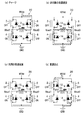
- FIGS. 3A to 3D and FIGS. 4E and 4F are explanatory diagrams of the operation mode of the H-bridge circuit. With reference to these explanatory diagrams, the operation mode of the H-bridge circuit 20 will be described.
- FIG. 3A shows a case where the two FETs diagonally opposed to each other are turned on to increase the absolute value of the motor current flowing through the stator winding 124. In the example shown in FIG. 3A, the FETs 4 and 6 are on, and the FETs 2 and 8 are off.
- an increase in the absolute value of the motor current is indicated by a black arrow. In this state, the motor current flows in the direction indicated by the broken line via FET6 ⁇ stator winding 124 ⁇ FET4, and the motor current increases. This operation mode is called charge mode.
- the FET 6 is turned off as shown in FIG. 3B.
- the FET 4 is kept on, and the FETs 2 and 8 are kept off.
- a current that loops through the FET 4, the diode 18 (the parasitic diode of the FET 8), and the stator winding 124 flows as shown by the broken line in the figure.
- This current is attenuated by the impedance of the FET 4, the diode 18 (the parasitic diode of the FET 8), and the stator winding 124, but the attenuation rate is low.
- This operation mode is called asynchronous low-speed decay mode.
- the attenuation of the motor current is indicated by a white arrow.
- the FET 8 may be further turned on as shown in FIG. Then, a motor current that loops through the FETs 4 and 8 and the stator winding 124 flows as indicated by the broken line in the figure. This current is attenuated by the impedances of the FETs 4 and 8 and the stator winding 124, but the attenuation rate is even slower.
- This operation mode is referred to as a synchronous slow decay mode.
- the attenuation of the motor current is indicated by a white arrow.
- the H bridge circuit 20 is set to the penetration prevention mode shown in FIG.
- FIG. 3D shows a penetration prevention mode in which FETs 2, 4, 6, and 8 are turned off.
- a counter electromotive force is generated in the stator winding 124. Therefore, a motor current flows in a direction indicated by a broken line through the diode 18 ⁇ the stator winding 124 ⁇ the diode 12 (the parasitic diode of the FET 2).
- the flyback mode is a mode in which a motor current flows in a direction indicated by a broken line via the diode 18 ⁇ the stator winding 124 ⁇ the FET 2.
- the motor current decay rate is slightly slower than in the penetration prevention mode.
- the back electromotive voltage mode is a mode in which the FETs 2, 4, 6, and 8 are in an off state, no current flows through the H bridge circuit 20, and a back electromotive voltage is generated.
- the free mode is a mode after the FETs 2, 4, 6, and 8 are in an off state, no current flows through the H-bridge circuit 20, and the back electromotive voltage has zero-crossed.
- the one-phase excitation drive of the two-phase stepping motor is commutated in the order of X + phase ⁇ Y + phase ⁇ X ⁇ phase ⁇ Y ⁇ phase, and sequentially shifts from the first quadrant to the fourth quadrant.
- the commutation is performed in the order of X + phase ⁇ Y ⁇ phase ⁇ X ⁇ phase ⁇ Y + phase.
- the H-bridge circuit 20 transitions in the order of charge mode ⁇ penetration prevention mode ⁇ flyback compatible mode ⁇ free mode.
- the CPU 101 performs control to repeat the charge mode and the slow decay mode as the operation mode when the current of the H bridge circuit 20 is limited.
- the CPU 101 makes a transition in the order of the penetration prevention mode, the flyback compatible mode, and the free mode after repeating the charge mode and the low-speed decay mode for each PWM cycle. . That is, when the current is limited, the H bridge circuit 20 repeats the charge mode and the low-speed decay mode every PWM cycle, and then transitions in the order of the penetration prevention mode ⁇ the flyback compatible mode ⁇ the free mode.
- the slow decay mode the current decay is less than in the fast decay mode.
- the low-speed attenuation mode can be handled only by the asynchronous low-speed attenuation mode, or can be shifted to the synchronous low-speed attenuation mode after the asynchronous low-speed attenuation mode.
- the kickback voltage is regenerated to the power supply via the parasitic diode (through prevention mode), and the upper side (high side) FET of this path is turned on to regenerate to the power supply (flyback compatible mode). Is possible.
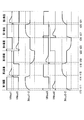
- FIG. 5 is a waveform diagram for explaining the current / voltage of the X phase and the Y phase of the H bridge circuit 20 of the comparative example.
- FIG. 6 is a waveform diagram for explaining the commutation order of the H-bridge circuit 20 of the comparative example.
- the operation of each quadrant will be described with reference to FIGS. 5 and 6.
- the H-bridge circuit 20X switches from the charge mode to the low-speed decay mode every PWM cycle, so that the coil current IMout1-0 The absolute value of is kept below the maximum current.
- the flyback pulse (kickback) generated in the reverse direction of the voltage applied in the immediately preceding fourth quadrant is generated in the Y-phase H bridge circuit 20Y.
- the H bridge circuit 20Y shifts to the free mode when the flyback voltage falls and the coil current IMout3-2 becomes zero.
- the H bridge circuit 20Y enters the free mode at time t11.
- a back electromotive force appears in the Y-phase H bridge circuit 20Y in the reverse direction of the kickback.
- the CPU 101 uses the zero cross of the back electromotive voltage as a trigger to shift to the next second quadrant.
- the kickback occurrence time and the back electromotive force vary depending on the motor driving voltage, the motor driving load, and the rotation speed. Note that the penetration prevention mode is inserted when necessary between the respective modes so that the upper and lower FETs of the half bridge are not simultaneously turned on. Thereby, a through current can be prevented.
- the stepping motor 120 is in the Y + phase
- the voltage VMout3 is the voltage MVdd.
- the flyback pulse (kickback) generated in the reverse direction of the voltage applied in the immediately preceding first quadrant is generated in the X-phase H bridge circuit 20X.
- the flyback voltage falls and the coil current IMout1-0 becomes 0, the H-bridge circuit 20X shifts to the free mode.
- the H bridge circuit 20X shifts to the free mode at time t15.
- a counter electromotive voltage appears in the reverse direction of kickback.
- the CPU 101 uses the back electromotive voltage zero crossing as a trigger to shift to the next third quadrant.
- the kickback occurrence time and the back electromotive force vary depending on the motor driving voltage, the motor driving load, and the rotation speed. Note that the penetration prevention mode is inserted when necessary between the respective modes so that the upper and lower FETs of the half bridge are not simultaneously turned on. Thereby, a through current can be prevented.
- the Y-phase H bridge circuit 20Y switches the voltage VMout3 to the voltage MVdd and the voltage VMout2 to the GND.
- the voltage MVdd is applied to the Y-phase stator winding 124Y, and the Y-phase coil current IMout3-2 gradually increases.
- the H-bridge circuit 20Y switches from the charge mode to the low-speed decay mode every PWM cycle, so that the coil current IMout3-2 The absolute value of is kept below the maximum current.
- ⁇ 3rd quadrant: time t18 >> At time t18 in the third quadrant, the X-phase H-bridge circuit 20X shifts to a charge mode in which the coil current IMout1-0 flows in the direction opposite to the first quadrant.
- the Y-phase H bridge circuit 20Y shifts to a flyback-compatible mode in which the coil current IMout3-2 flows in the direction opposite to the first quadrant.
- the stepping motor 120 is in the X-phase
- the voltage VMout0 is the voltage MVdd.
- the voltage VMout1 is switched to GND and the voltage VMout0 is switched to the voltage MVdd.
- a voltage is applied to the X-phase stator winding 124X in the direction opposite to the first quadrant, and the X-phase coil current IMout1-0 gradually increases in the direction opposite to the first quadrant.
- the flyback pulse (kickback) generated in the reverse direction of the voltage applied in the immediately preceding second quadrant is generated in the Y-phase H bridge circuit 20Y.
- the H bridge circuit 20Y shifts to the free mode when the flyback voltage falls and the coil current IMout3-2 becomes zero.
- the H bridge circuit 20Y shifts to the free mode at time t19.
- a back electromotive force appears in the Y-phase H bridge circuit 20Y in the reverse direction of the kickback.
- the CPU 101 commutates using the zero cross of the back electromotive voltage as a trigger, and shifts to the next fourth quadrant.
- the kickback occurrence time and the back electromotive force vary depending on the motor driving voltage, the motor driving load, and the rotation speed.
- the operation in the third quadrant is the same as that in the first quadrant except for the direction of current flow.
- ⁇ 4th quadrant time t22 >>
- the X-phase H bridge circuit 20X shifts to the flyback mode.
- the Y-phase H bridge circuit 20Y shifts to the charge mode.
- the stepping motor 120 is in the Y-phase
- the voltage VMout2 is the voltage MVdd.
- the flyback pulse (kickback) generated in the reverse direction of the voltage applied in the immediately preceding third quadrant is generated in the X-phase H bridge circuit 20X.
- the flyback voltage falls and the coil current IMout1-0 becomes 0, the H-bridge circuit 20X shifts to the free mode.
- the H bridge circuit 20X shifts to the free mode at time t23.
- a counter electromotive voltage appears in the reverse direction of kickback in the X-phase H-bridge circuit 20X.
- the CPU 101 uses the back electromotive voltage zero crossing as a trigger to shift to the next third quadrant.
- the kickback occurrence time and the back electromotive force vary depending on the motor driving voltage, the motor driving load, and the rotation speed.
- the Y-phase H bridge circuit 20Y switches the voltage VMout3 to GND and the voltage VMout2 to the voltage MVdd.
- the voltage MVdd is applied to the Y-phase stator winding 124Y in the direction opposite to the second quadrant, and the Y-phase coil current IMout3-2 gradually increases in the direction opposite to the second quadrant.
- the operation in the fourth quadrant is the same as that in the second quadrant except for the direction of current flow. ⁇ Following quadrant ⁇
- the H bridge circuits 20X and 20Y operate while sequentially switching operations similar to those in the first to fourth quadrants described above.
- FIG. 7 is a flowchart for explaining processing of the first quadrant of the X phase in the comparative example.
- the CPU 101 sets the maximum duty for each PWM cycle, sets a value in the delay timer (processing S10), and the X-phase H bridge circuit 20X shifts to the energization period. During this energization period, the X-phase H-bridge circuit 20X shifts to the charge mode.
- the CPU 101 turns on the FET 2 that is on the high side (HS) side of the connection point Mout1, and further turns on the FET 8 that is on the low side (LS) side of the connection point Mout0 (processing S11). Subsequently, the CPU 101 starts an energization timer (processing S12).
- CPU 101 determines whether or not the maximum time related to the Y phase has elapsed (processing S13). If the CPU 101 determines that the maximum time related to the Y phase has not elapsed (processing S13 ⁇ No), the CPU 101 determines the zero cross of the back electromotive voltage of the Y phase (processing S14). If the CPU 101 determines that the Y-phase back electromotive force voltage has not zero-crossed (step S14 ⁇ No), the CPU 101 returns to step S13.
- step S15 the CPU 101 subtracts the delay timer (step S15). If the CPU 101 determines that the delay timer is not 0 (step S16 ⁇ No), the CPU 101 returns to step S13. When the delay timer becomes 0 (processing S16 ⁇ Yes), the CPU 101 turns off the FET 2 on the high side (HS) side of the connection point Mout1 and the FET 8 on the low side (LS) side of the connection point Mout0. Then, the energization period ends (processing S17).
- processing S13 determines that the maximum time related to the Y phase has elapsed in the processing S13 (processing S13 ⁇ Yes), regardless of the determination of the zero cross of the back electromotive voltage of the Y phase and the count value of the delay timer, Processing S17 is performed and an energization period is ended. After the energization period ends, the CPU 101 ends the energization timer, calculates the speed based on the value of the energization timer (process S18), and ends the process in the first quadrant of the X phase.
- the processing in the second quadrant of the Y phase is the same as the processing in the first quadrant of the X phase.
- the process in the third quadrant of the X phase is the same as the process in the first quadrant of the X phase except that the direction of the voltage applied to the stator winding 124X (see FIG. 1) is different.
- the processing in the fourth quadrant of the Y phase is the same as the processing in the first quadrant of the X phase except that the direction of the voltage applied to the stator winding 124Y (see FIG. 1) is different.
- FIG. 8 is a flowchart for explaining processing of the second quadrant of the X phase in the comparative example.
- the CPU 101 sets the maximum time in the timer (processing S30).
- the X-phase H bridge circuit 20X shifts to the flyback period. In the flyback period, the X-phase H bridge circuit 20X shifts to the flyback mode.
- the H bridge circuit 20X shifts to the counter electromotive voltage period.
- the X-phase H bridge circuit 20X shifts to the counter electromotive voltage mode.
- the end of the flyback compatible mode can be detected by any one of the fall of the flyback voltage, the zero cross of the flyback voltage, and the zero cross of the coil current.
- the H bridge circuit 20X shifts to the free period.
- the X-phase H-bridge circuit 20X shifts to the free mode.
- the end of the back electromotive voltage mode can be detected by a zero cross of the back electromotive voltage. If the back electromotive voltage does not exceed 0V due to overload, the back electromotive voltage mode ends after a delay time from the back electromotive voltage peak (e.g., approximately twice the time from the start of the back electromotive voltage mode to the peak). It can be detected by the voltage increase next to the peak of the back electromotive voltage.
- step S34 ⁇ Yes the CPU 101 ends the process of the second quadrant of the X phase.
- the CPU 101 returns to the process S31 and determines that the maximum time has been exceeded. If the timer exceeds the maximum time (step S31 ⁇ Yes), the CPU 101 ends the processing in the second quadrant of the X phase regardless of the operation mode.
- the processing in the second quadrant of the X phase is the same as the processing in the third quadrant of the Y phase.
- the processing in the fourth quadrant of the X phase is similar to the processing in the second quadrant of the X phase except that the direction of the zero crossing voltage is different.
- the process in the third quadrant of the Y phase is the same as the process in the first quadrant of the Y phase except that the direction of the zero crossing voltage is different.
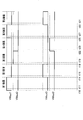
- FIG. 9 is a waveform diagram illustrating the current / voltage of the X phase and the Y phase of the H bridge circuit 20 in the present embodiment.
- FIG. 10 is a waveform diagram for explaining the commutation order of the H-bridge circuit 20 in the present embodiment.
- the operation of each quadrant will be described with reference to FIGS. 9 and 10.
- time t40 First quadrant: time t40 >> At time t40 in the first quadrant, the X-phase H bridge circuit 20X shifts to the charge mode, and the Y-phase H bridge circuit 20Y shifts to the flyback mode. As shown in FIG. 10, the stepping motor 120 is in the X + phase, and the voltage VMout1 is the voltage MVdd.
- the voltage VMout1 in the charge mode, the voltage VMout1 is switched to the voltage MVdd, and the voltage VMout0 is switched to GND.
- the voltage MVdd is applied to the X-phase stator winding 124X, and the X-phase coil current IMout1-0 gradually increases.
- the H-bridge circuit 20X switches from the charge mode to the low-speed decay mode every PWM cycle, so that the coil current IMout1-0 The absolute value of is kept below the maximum current.
- the flyback pulse (kickback) generated in the reverse direction of the voltage applied in the immediately preceding fourth quadrant is generated in the Y-phase H bridge circuit 20Y.
- the H bridge circuit 20Y shifts to the free mode when the flyback voltage falls and the coil current IMout3-2 becomes zero.
- the H bridge circuit 20Y shifts to the free mode at time t41.
- a back electromotive force appears in the Y-phase H bridge circuit 20Y in the reverse direction of the kickback.
- the CPU 101 uses the zero cross of the back electromotive voltage as a trigger to shift to the next second quadrant.
- the kickback occurrence time and the back electromotive force vary depending on the motor driving voltage, the motor driving load, and the rotation speed. Note that the penetration prevention mode is inserted when necessary between the respective modes so that the upper and lower FETs of the half bridge are not simultaneously turned on. Thereby, a through current can be prevented.
- time t44 Second quadrant: time t44 >> At time t44 in the second quadrant, the X-phase H-bridge circuit 20X shifts to the flyback mode, and the Y-phase H-bridge circuit 20Y shifts to the charge mode. As shown in FIG. 10, the stepping motor 120 is in the Y + phase, and the voltage VMout3 is the voltage MVdd.
- a flyback pulse generated in the reverse direction of the voltage applied in the immediately preceding first quadrant is generated in the X-phase H-bridge circuit 20X.
- the flyback voltage falls and the coil current IMout1-0 becomes 0, the H-bridge circuit 20X shifts to the free mode.
- the H bridge circuit 20X shifts to the free mode at time t45.
- a counter electromotive voltage appears in the reverse direction of kickback.
- the CPU 101 uses the back electromotive voltage zero crossing as a trigger to shift to the next third quadrant.
- the kickback occurrence time and the back electromotive force vary depending on the motor driving voltage, the motor driving load, and the rotation speed. Note that the penetration prevention mode is inserted when necessary between the respective modes so that the upper and lower FETs of the half bridge are not simultaneously turned on. Thereby, a through current can be prevented.
- the Y-phase H bridge circuit 20Y switches the voltage VMout3 to the voltage MVdd and the voltage VMout2 to the GND.
- the voltage MVdd is applied to the Y-phase stator winding 124Y, and the Y-phase coil current IMout3-2 gradually increases.
- the H-bridge circuit 20Y switches from the charge mode to the low-speed decay mode every PWM cycle, so that the coil current IMout3-2 The absolute value of is kept below the maximum current.
- deceleration stop control is in progress from the deceleration start step to the deceleration stop step.
- the number of deceleration steps is four.
- the stepping motor 120 reaches the final stop speed.
- the deceleration start step is calculated from the number of drive steps and the number of deceleration steps.
- ⁇ 3rd quadrant Time t48: Deceleration start step >>
- the X-phase H bridge circuit 20X shifts to a charge mode in the direction opposite to that in the first quadrant.
- the Y-phase H bridge circuit 20Y shifts to a flyback-compatible mode in which the coil current IMout3-2 flows in the direction opposite to the first quadrant.
- the third quadrant is a step for starting the deceleration of the stepping motor 120. As shown in FIG. 10, the stepping motor 120 is in the X-phase, and the voltage VMout0 is the voltage MVdd.
- the voltage VMout1 is switched to GND and the voltage VMout0 is switched to the voltage MVdd.
- a voltage is applied to the X-phase stator winding 124X in the direction opposite to the first quadrant, and the X-phase coil current IMout1-0 gradually increases in the direction opposite to the first quadrant.
- the operation in the third quadrant is the same as that in the first quadrant except for the direction of current flow.
- the flyback pulse (kickback) generated in the reverse direction of the voltage applied in the immediately preceding second quadrant is generated in the Y-phase H bridge circuit 20Y.
- the H bridge circuit 20Y shifts to the free mode when the flyback voltage falls and the coil current IMout3-2 becomes zero.
- the H bridge circuit 20Y shifts to the free mode at time t49.
- a back electromotive force appears in the Y-phase H bridge circuit 20Y in the reverse direction of the kickback.
- the kickback occurrence time and the back electromotive force vary depending on the motor driving voltage, the motor driving load, and the rotation speed.
- the CPU 101 instructs the H bridge circuits 20X and 20Y to Specify the slow decay mode for each PWM cycle.
- the CPU 101 calculates the time of the first step of the deceleration step from the time of the immediately preceding step measured by the timer, the preset maximum speed, and the number of deceleration steps.
- the CPU 101 performs commutation using this time as a trigger instead of the zero cross of the back electromotive voltage, and shifts to the next fourth quadrant.
- the absolute value of the X-phase coil current IMout1-0 may increase sharply.
- the H bridge circuit 20X prevents overcurrent by shifting to the low-speed decay mode by current control for each PWM period.
- the absolute value of the coil current IMout1-0 slightly increases, but the H-bridge circuit 20X has not shifted to the low-speed attenuation mode.
- the penetration prevention mode is inserted when necessary between the respective modes so that the upper and lower FETs of the half bridge are not simultaneously turned on. Thereby, a through current can be prevented.
- ⁇ 4th quadrant Time t52: Second step of deceleration >>
- the X-phase H bridge circuit 20X shifts to the flyback compatible mode in the direction opposite to that in the second quadrant.
- the Y-phase H bridge circuit 20Y shifts to a charge mode in the direction opposite to that of the second quadrant.
- This fourth quadrant is the second step of deceleration of the stepping motor 120. As shown in FIG. 10, the stepping motor 120 is in the Y-phase, and the voltage VMout2 is the voltage MVdd.
- the Y-phase H bridge circuit 20Y switches the voltage VMout3 to GND and the voltage VMout2 to the voltage MVdd in the charge mode.
- the voltage MVdd is applied to the Y-phase stator winding 124Y in the direction opposite to the second quadrant, and the Y-phase coil current IMout3-2 gradually increases in the direction opposite to the second quadrant.
- the operation in the fourth quadrant is the same as that in the second quadrant except for the direction of current flow.
- a flyback pulse that occurs in the reverse direction of the voltage applied in the immediately preceding third quadrant is generated.
- the flyback voltage falls and the coil current IMout1-0 becomes 0, the H-bridge circuit 20X shifts to the free mode.
- the H bridge circuit 20X shifts to the free mode at time t53.
- a counter electromotive voltage appears in the reverse direction of kickback in the X-phase H-bridge circuit 20X.
- the kickback occurrence time and the back electromotive voltage vary depending on the motor drive voltage, the motor drive load, and the rotational speed.
- the CPU 101 instructs the H bridge circuits 20X and 20Y to Specify the slow decay mode for each PWM cycle.
- the CPU 101 calculates the time of the first step of the deceleration step from the time of the immediately preceding step measured by the timer, the preset maximum speed, and the number of deceleration steps.
- the CPU 101 performs commutation using this time as a trigger instead of the zero cross of the back electromotive voltage, and shifts to the next first quadrant.
- the H bridge circuit 20Y prevents an overcurrent by shifting to the low-speed decay mode by current control every PWM cycle.
- the absolute value of the coil current IMout3-2 slightly increases, but the H-bridge circuit 20Y has not shifted to the low-speed attenuation mode.
- the penetration prevention mode is inserted when necessary between the respective modes so that the upper and lower FETs of the half bridge are not simultaneously turned on. Thereby, a through current can be prevented.
- First quadrant Time t56: Third step of deceleration >> At time t56 in the first quadrant, the X-phase H-bridge circuit 20X shifts to the charge mode. The Y-phase H bridge circuit 20Y shifts to the flyback mode. This first quadrant is the third step of deceleration of the stepping motor 120. As shown in FIG. 10, the stepping motor 120 is in the X + phase, and the voltage VMout1 is the voltage MVdd. As shown in FIG. 9, in the X-phase H bridge circuit 20X, in the charge mode, the voltage VMout0 is switched to the voltage MVdd and the voltage VMout1 is switched to GND. The voltage MVdd is applied to the X-phase stator winding 124X, and the X-phase coil current IMout1-0 gradually increases.
- the flyback pulse (kickback) generated in the reverse direction of the voltage applied in the immediately preceding fourth quadrant is generated in the Y-phase H bridge circuit 20Y.
- the H bridge circuit 20Y shifts to the free mode when the flyback voltage falls and the coil current IMout3-2 becomes zero.
- the H bridge circuit 20Y shifts to the free mode at time t57.
- a back electromotive force appears in the Y-phase H bridge circuit 20Y in the reverse direction of the kickback.
- the kickback occurrence time and the back electromotive force vary depending on the motor driving voltage, the motor driving load, and the rotation speed.
- the operation of the first quadrant so far is the same as that of the third quadrant except for the direction of current flow.
- the CPU 101 instructs the H bridge circuits 20X and 20Y to Specify the slow decay mode for each PWM cycle.
- the CPU 101 calculates the time of the first step of the deceleration step from the time of the previous quadrant step measured by the timer, the preset maximum speed, and the number of deceleration steps.
- the CPU 101 performs commutation using this time as a trigger instead of the zero cross of the back electromotive voltage, and shifts to the next fourth quadrant.
- the absolute value of the X-phase coil current IMout1-0 may increase sharply.
- the H bridge circuit 20X prevents overcurrent by shifting to the low-speed decay mode by current control for each PWM period.
- the absolute value of the coil current IMout1-0 slightly increases, but the H-bridge circuit 20X has not shifted to the low-speed attenuation mode.
- the penetration prevention mode is inserted when necessary between the respective modes so that the upper and lower FETs of the half bridge are not simultaneously turned on. Thereby, a through current can be prevented.
- Second quadrant Time t60: Deceleration stop step >> At time t60 in the second quadrant, the X-phase H-bridge circuit 20X shifts to the flyback mode. The Y-phase H bridge circuit 20Y shifts to the charge mode. This second quadrant is a deceleration stop step of the stepping motor 120. As shown in FIG. 10, the stepping motor 120 is in the Y + phase, and the voltage VMout3 is the voltage MVdd.
- the voltage VMout3 is switched to the voltage MVdd and the voltage VMout2 is switched to GND.
- the voltage MVdd is applied to the Y-phase stator winding 124Y, and the Y-phase coil current IMout3-2 gradually increases.
- the operation in the second quadrant is the same as that in the fourth quadrant except for the direction of current flow.
- a flyback pulse that occurs in the reverse direction of the voltage applied in the immediately preceding third quadrant is generated.
- the flyback voltage falls and the coil current IMout1-0 becomes 0, the H-bridge circuit 20X shifts to the free mode.
- the H bridge circuit 20X shifts to the free mode at time t61.
- a counter electromotive voltage appears in the reverse direction of kickback in the X-phase H-bridge circuit 20X.
- the kickback occurrence time and the back electromotive voltage vary depending on the motor drive voltage, the motor drive load, and the rotational speed.
- the CPU 101 instructs the H bridge circuits 20X and 20Y to Specify the slow decay mode for each PWM cycle.
- the CPU 101 calculates the time of the first step of the deceleration step from the time of the previous quadrant step measured by the timer, the preset maximum speed, and the number of deceleration steps.
- the CPU 101 performs commutation using this time as a trigger instead of the zero cross of the back electromotive voltage, and shifts to the next third quadrant.
- the absolute value of the Y-phase coil current IMout3-2 may increase sharply.
- the H bridge circuit 20Y prevents an overcurrent by shifting to the low-speed decay mode by current control every PWM cycle.
- the H-bridge circuit 20Y since the absolute value of the coil current IMout3-2 has increased beyond the threshold after time t62, the H-bridge circuit 20Y periodically shifts to the low-speed decay mode. As a result, the stepping motor 120 reaches the final stop speed and can be stopped at a desired rotational position.
- the on-duty can be gradually reduced from 100% and decelerated within a range where the coil current does not affect the driving of the motor and the final position holding.
- the on-duty is the FET on-time for each PWM period.
- the commutation is preferably triggered by the zero cross of the back electromotive force as a trigger.
- the step-out detection can be determined by the deviation of the kickback time and the back electromotive voltage.
- FIG. 11 is a flowchart for explaining processing of the first quadrant of the X phase in the present embodiment.
- the processing after the stop control start position is different from the comparative example shown in FIG.
- the CPU 101 sets a stop control timer after the stop control start position, and further operates with the stop control timer instead of the Y-phase counter electromotive voltage zero cross after (stop control start position + 1).
- the CPU 101 sets the maximum duty for each PWM cycle, and sets a value in the delay timer (processing S50).
- the X-phase H bridge circuit 20X shifts to the energization period. During this energization period, the X-phase H-bridge circuit 20X shifts to the charge mode.
- the CPU 101 turns on the FET 2 on the high side (HS) side of the connection point Mout1, and further turns on the FET 8 on the low side (LS) side of the connection point Mout0 (processing S51). Subsequently, the CPU 101 starts an energization timer (processing S52).
- the CPU 101 determines whether the rotational position of the motor is equal to or greater than (stop control start position + 1) (processing S53). If it is equal to or greater than (stop control start position + 1) (process S53 ⁇ Yes), the CPU 101 starts stop control. The CPU 101 subtracts the stop control timer (process S58), repeats the processes S59 and S58 until the timer value becomes 0, and then proceeds to process S60. If the rotational position of the motor is less than (stop control start position + 1) (process S53 ⁇ No), the CPU 101 proceeds to process S54 and performs the normal first quadrant process.
- process S54 the CPU 101 determines whether or not the maximum time related to the Y phase has elapsed. If the CPU 101 determines that the maximum time related to the Y phase has not elapsed (processing S54 ⁇ No), the CPU 101 determines the zero cross of the back electromotive voltage of the Y phase (processing S55). If the CPU 101 determines that the Y-phase back electromotive force voltage has not zero-crossed (step S55 ⁇ No), the CPU 101 returns to step S54.
- the CPU 101 determines that the zero-cross of the back electromotive voltage of the Y phase is determined (processing S55 ⁇ Yes)
- the CPU 101 subtracts the delay timer (processing S56). If the CPU 101 determines that the delay timer is not 0 (step S57 ⁇ No), the CPU 101 returns to step S54.
- the energization timer becomes 0 (processing S57 ⁇ Yes)
- the CPU 101 proceeds to processing S60, and FET2 which is the high side (HS) side of the connection point Mout1 and FET8 which is the low side (LS) side of the connection point Mout0. And turn off the power supply period.
- processing S60 is performed and an energization period is ended.
- the CPU 101 ends the energization timer and calculates the speed based on the value of this energization timer (processing S61).
- CPU101 will set a stop control timer (process S63). Then, the CPU 101 ends the process in the first quadrant of the X phase.
- the processing of the second quadrant of the X phase by the motor drive control device of the present embodiment is the same as the processing of the comparative example shown in FIG.
- FIG. 12 is a flowchart illustrating the process of the energization side PWM cycle in the present embodiment.
- “energization” is composed of one or more “energization-side PWM cycles” performed every PWM cycle.
- the process of the energization side PWM cycle is always necessary to limit the maximum current during stop control, including normal time. In one-phase excitation drive, a method that does not use a PWM cycle is common.
- step S70 ⁇ Yes the CPU 101 sets the coil current threshold (step S71), and proceeds to step S72. If the CPU 101 is not the first cycle of the PWM cycle in this quadrant (step S70 ⁇ No), the CPU 101 proceeds to step S72. If the coil current exceeds the threshold value (processing S72 ⁇ Yes), the CPU 101 shifts the H bridge circuit 20 to the low-speed attenuation mode (processing S73), and proceeds to processing S74. If the coil current does not exceed the threshold value (processing S72 ⁇ No), the CPU 101 proceeds to processing S74.
- the CPU 101 shifts to the charge mode (process S75). If the H-bridge circuit 20 is in the low-speed decay mode (process S74 ⁇ Yes), the CPU 101 is energized. The end of the side PWM cycle is determined (process S76). The CPU 101 repeats these processes S72 to S75 until the energization side PWM cycle ends (process S76 ⁇ No).
- FIG. 13 is a flowchart for explaining processing of a PWM cycle on the counter electromotive (non-energized) side in the present embodiment.
- the counter electromotive side refers to the non-energized side of the PWM cycle, and the processing of the PWM cycle on this side is performed every PWM cycle.
- step S80 ⁇ Yes If the counter electromotive side PWM cycle is started and the PWM cycle is the first cycle in this quadrant (processing S80 ⁇ Yes), the CPU 101 shifts the H bridge circuit 20 to the flyback compatible mode (processing S81), and processing Proceed to S82. If it is not the first cycle of the PWM cycle in this quadrant (step S80 ⁇ No), the CPU 101 proceeds to step S82.
- step S82 ⁇ Yes If the H bridge circuit 20 is not in the flyback compatible mode (step S82 ⁇ Yes), the process proceeds to step S85. If the H-bridge circuit 20 is in the flyback compatible mode (processing S82 ⁇ Yes) and this flyback compatible mode continues (No), the process proceeds to processing S88.
- process S85 if the H-bridge circuit 20 is not in the back electromotive voltage mode (process S85 ⁇ No), or if the back electromotive voltage mode is completed (process S86 ⁇ Yes), the H bridge circuit 20 shifts to the free mode (process S87). Proceed to step S88. If the H-bridge circuit 20 is in the counter electromotive voltage mode (process S85 ⁇ Yes) and the counter electromotive voltage mode is continued (process S86 ⁇ No), the process proceeds to process S88. The CPU 101 and the H bridge circuit 20 repeat these processes S82 to S87 until the energization side PWM cycle is completed (process S88 ⁇ No).
- the CPU 101 when stopping the driving of the stepping motor 120, the CPU 101 performs step-by-step processing until the speed decreases from the calculated deceleration start step to a predetermined rotational speed that can be stopped at a desired position. Perform extended control of commutation time. More specifically, when the CPU 101 stops the driving of the stepping motor 120, the speed reduction control that increases the phase switching (commutation) time according to the following deceleration step to a speed at which the stop position accuracy of the stepping motor 120 can be ensured. To ensure position accuracy with a small number of steps.
- the CPU 101 performs control to stop commutation based on the zero cross of the back electromotive force voltage from the deceleration start step until the stepping motor 120 becomes equal to or lower than the predetermined rotation speed, and lengthen the commutation time for each step. Specifically, the CPU 101 measures the time of one-phase excitation immediately before the deceleration, and gradually increases the phase switching (commutation) time to control the time, thereby reducing the motor rotation speed.
- the time increase may be, for example, increasing the commutation time for each step at a constant rate (eg, extending the time by 25% at each step). This is shown in the following formula (1).
- FIG. 14 shows the relationship between speed and time by this deceleration control method.
- This deceleration control method is characterized in that the average speed decrease immediately after the start of deceleration is large and the average speed decrease immediately before the end of deceleration is small.
- the motor rotation speed may be further reduced by using in combination with duty control that intentionally gradually decreases the duty for each PWM cycle of single-phase excitation. For example, by reducing the duty by 10%, 90% ⁇ 80% ⁇ 70% ⁇ 60%. In this case, if commutation is performed using the zero cross of the back electromotive force as a trigger, for example, when the load increases due to the rotation of the motor, the current required for lifting the load may be insufficient. Flow) It is better to use time control that gradually extends the time. The effect on speed reduction by this duty control varies depending on the motor, voltage and load.
- the CPU 101 controls to repeat the charge mode and the low-speed decay mode. This reduces the current ripple.
- the present invention is not limited to the above embodiment, and can be modified without departing from the spirit of the present invention.
- the type of motor is not limited to a stepping motor, and includes a brushless DC motor.
- B It is also possible to gradually reduce the on-duty from 100% within a range where the coil current does not affect the driving of the motor and the final position holding.
- the on-duty means the on-time of the FET for each PWM cycle.
- C The CPU 101 may perform the extension control of the commutation time for each step by setting a stop control value in the energization timer without using the stop control timer.
- Motor control device 101 CPU (an example of control means) 107 bridge control unit 110 bridge control circuit 113 PWM signal generator 114 comparator 115 D / A converter 116 current detection unit (an example of current detection means) 118 BEMF detector (an example of zero-cross detection means) 120 Stepping motors 122XN, 122XP, 122YN, 122YP Stator 124, 124X, 124Y Stator winding (an example of a motor coil) 126 Rotor 130 Host device 140 DC power supply 142 Ground wire 20, 20X, 20Y H bridge circuit 2, 4, 6, 8, 15, 17 FET 12, 14, 16, 18 Diode Icoil Current measurement value Iref Current reference value VM Motor voltage Mout0, Mout1, Mout2, Mout3 Connection point VMout0, VMout1, VMout2, VMout3 Voltage MVdd Voltage IMout1-0, IMout3-2 Coil current
Landscapes
- Engineering & Computer Science (AREA)
- Power Engineering (AREA)
- Control Of Stepping Motors (AREA)
Abstract
モータの回転停止位置を正確に制御する。 モータ制御装置(100)は、モータに設けられたモータコイルの逆起電圧のゼロクロスを検知するBEMF検出部(118)と、モータを1相励磁方式かつ位置センサレスで駆動制御し、BEMF検出部(118)によって検知された逆起電圧のゼロクロスに基づいて転流し、駆動電圧と負荷に応じた回転速度によってモータの駆動制御を行うと共に、モータの駆動を停止する際には、算出された減速開始ステップから所望の位置で停止可能な所定回転速度以下に低下するまで、ステップ毎の転流時間の延長制御を行うCPU(101)とを備える。
Description
本発明は、モータの回転停止位置を制御するのに好適なモータ駆動制御装置およびモータ駆動制御方法に関する。
従来、ステッピングモータを1相励磁で、逆起電圧のゼロクロスをトリガに転流する位置センサレス駆動を行うと、駆動電圧と負荷に応じた負荷電流と回転速度でモータが回転する。このモータの駆動を停止すると、モータの慣性により、オーバーランが発生し、位置精度が悪化する。
モータを停止するため、駆動回路(Hブリッジ回路)の全てのスイッチング素子(FET)をオフすると、逆起電圧が周期的に変化し、モータが慣性で回転していることが観測される。
モータの停止と同時に、2相励磁でホールド電流を高く設定して、徐々に電流を減少させ、2相励磁の安定点で停止するように制御するホールド電流減衰制御方法では、モータの回転速度が低速で慣性が小さい場合は位置精度の確保が可能であるが、モータの回転速度が高速で慣性が大きい場合、制御中に電流が周期的に変化し、モータが慣性で回転していることが観測できる。
このため、上記のホールド電流減衰制御中に、過大な電流が発生した場合、逆方向に電圧を印加する高速減衰(Fast Decay)制御を用いて、電流を消費するようにすると、ホールド電流減衰制御よりも位置精度の確保が可能であるが、電気角の1象限を超えるモータの慣性の場合、位置精度を確保できない。
例えば、特許文献1には、回転速度が速い場合でも、ロータの停止位置を正確に制御することができるステッピングモータの制御方法が開示されている。
例えば、特許文献1には、回転速度が速い場合でも、ロータの停止位置を正確に制御することができるステッピングモータの制御方法が開示されている。
特許文献1の制御方法は、1相励磁のオープン制御であり、停止直前の回転速度は任意であるが固定されている。1相励磁のオープン制御は、負荷に応じた最適な回転速度にはならず、また、負荷によってモータの振動がおさまる時間がばらつく。位置センサレス駆動は、駆動電圧あるいは負荷により停止直前の回転速度が安定しないため、停止直前の1ステップで保持時間を延長する場合、慣性によるオーバーランが発生することも含め、停止位置を正確に制御することが困難となるおそれがある。つまり、回転状態によっては、所望の停止位置に短時間で制御するには不十分である。
そこで、本発明は、モータ駆動制御装置およびモータ駆動制御方法について、モータの回転停止位置を短時間で正確に制御することを課題とする。
そこで、本発明は、モータ駆動制御装置およびモータ駆動制御方法について、モータの回転停止位置を短時間で正確に制御することを課題とする。
前記した課題を解決するため、本発明のモータ駆動制御装置は、モータに設けられたモータコイルの逆起電圧のゼロクロスを検知するゼロクロス検知手段と、このモータを1相励磁方式かつ位置センサレスで駆動制御し、前記ゼロクロス検知手段によって検知された前記逆起電圧のゼロクロスに基づいて転流し、駆動電圧と負荷に応じた回転速度によって前記モータの駆動制御を行うと共に、前記モータの駆動を停止する際には、算出された減速開始ステップから所望の位置で停止可能な所定回転速度以下に低下するまで、ステップ毎の転流時間の延長制御を行う制御手段とを備える。
その他の手段については、発明を実施するための形態のなかで説明する。
その他の手段については、発明を実施するための形態のなかで説明する。
本発明によれば、モータ駆動制御装置およびモータ駆動制御方法について、モータの回転停止位置を短時間で正確に制御することが可能となる。
以降、本発明を実施するための形態を、各図を参照して詳細に説明する。
図1は、本実施形態および比較例のモータ制御システムの全体ブロック図である。
図1において、ステッピングモータ120は、バイポーラ型2相ステッピングモータであり、永久磁石を有し回動自在に設けられた回転子126と、回転子126の周囲の周回方向4等分位置に設けられた固定子とを有している。これらの固定子は、X相の固定子122XP,122XNと、Y相の固定子122YP,122YNとからなる。これらの固定子には各々巻線が巻回されている。固定子122YP,122YNに巻回された巻線は直列に接続されており、両巻線を合わせて「固定子巻線124Y」という。同様に、固定子122XP,122XNに巻回された巻線は直列に接続されており、両巻線を合わせて「固定子巻線124X」という。固定子巻線124Y,124Xは、モータコイルの一例である。
図1において、ステッピングモータ120は、バイポーラ型2相ステッピングモータであり、永久磁石を有し回動自在に設けられた回転子126と、回転子126の周囲の周回方向4等分位置に設けられた固定子とを有している。これらの固定子は、X相の固定子122XP,122XNと、Y相の固定子122YP,122YNとからなる。これらの固定子には各々巻線が巻回されている。固定子122YP,122YNに巻回された巻線は直列に接続されており、両巻線を合わせて「固定子巻線124Y」という。同様に、固定子122XP,122XNに巻回された巻線は直列に接続されており、両巻線を合わせて「固定子巻線124X」という。固定子巻線124Y,124Xは、モータコイルの一例である。
上位装置130は、ステッピングモータ120の回転速度を指令する速度指令信号を出力する。モータ制御装置100は、この速度指令信号に応じてステッピングモータ120を駆動制御するものである。モータ制御装置100には、固定子巻線に接続されたハーフブリッジを組み合わせたHブリッジ回路20X,20Yが設けられており、それぞれ固定子巻線124X,124Yに対して、X相電圧VMX,Y相電圧VMYを印加する。
Hブリッジ回路20Xは、接続点Mout0を介してX相の固定子122XNの巻線(モータコイルの一例)と接続され、更に接続点Mout1を介してX相の固定子122XPの巻線(モータコイルの一例)と接続される。コイル電流IMout1-0は、接続点Mout1から接続点Mout0へ流れる電流である。
Hブリッジ回路20Yは、接続点Mout2を介してY相の固定子122YPの巻線(モータコイルの一例)と接続され、更に接続点Mout3を介してY相の固定子122YNの巻線(モータコイルの一例)と接続される。コイル電流IMout3-2は、接続点Mout3から接続点Mout2へ流れる電流である。
Hブリッジ回路20Xは、接続点Mout0を介してX相の固定子122XNの巻線(モータコイルの一例)と接続され、更に接続点Mout1を介してX相の固定子122XPの巻線(モータコイルの一例)と接続される。コイル電流IMout1-0は、接続点Mout1から接続点Mout0へ流れる電流である。
Hブリッジ回路20Yは、接続点Mout2を介してY相の固定子122YPの巻線(モータコイルの一例)と接続され、更に接続点Mout3を介してY相の固定子122YNの巻線(モータコイルの一例)と接続される。コイル電流IMout3-2は、接続点Mout3から接続点Mout2へ流れる電流である。
(モータ制御装置100)
次に、図2を参照し、モータ制御装置100の詳細を説明する。なお、図1には2系統の固定子巻線124X,124Yと、2系統のHブリッジ回路20X,20Yを示したが、図2では、これらをまとめて1系統の固定子巻線124と、1系統のHブリッジ回路20として示している。
次に、図2を参照し、モータ制御装置100の詳細を説明する。なお、図1には2系統の固定子巻線124X,124Yと、2系統のHブリッジ回路20X,20Yを示したが、図2では、これらをまとめて1系統の固定子巻線124と、1系統のHブリッジ回路20として示している。
モータ制御装置100の内部に設けられたCPU(Central Processing Unit)101(制御手段の一例)は、ROM(Read Only Memory)103に記憶された制御プログラムに基づいて、バス106を介して各部を制御する。RAM(Random Access Memory)102は、CPU101のワークメモリとして使用される。タイマ(timer)104は、CPU101の制御の下、リセットされたタイミングからの経過時間を測定する。I/Oポート(I/O Port)105は、図1に示した上位装置130、その他外部装置との間で信号を入出力する。ブリッジ制御部107は、CPU101からの指令に基づいて、ブリッジ制御回路110の各部を制御する。
ここで、ブリッジ制御回路110は、一体の集積回路として構成されている。その内部においてPWM(Pulse Width Modulation)信号発生器113は、ブリッジ制御部107による制御に基づいて、PWM信号を生成しHブリッジ回路20に供給する。Hブリッジ回路20には、FET(Field-Effect Transistor)2,4,6,8と、FET15,17とが含まれている。なお、図中においてこれらFETの下側の端子がソース端、上側の端子がドレイン端になる。PWM信号とは、これらFETにゲート電圧として印加されるオン(ON)/オフ(OFF)信号である。
FET2,4は直列に接続され、その直列回路に対して、直流電源140およびアース線142が接続され、所定の電圧MVddが印加される。同様に、FET6,8も直列に接続され、その直列回路に対して電圧MVddが印加される。ダイオード12,14,16,18は、還流用の寄生ダイオードであり、FET2,4,6,8に対して並列に接続されている。FET15,17は、電流検出用に設けられているものであり、それぞれFET4,8と共にカレントミラー回路を形成している。これにより、FET4,8に流れる電流に比例する電流が、それぞれFET15,17に流れる。
FET2,4の接続点Mout0における電圧VMout0は、モータの固定子巻線124の一端に印加される。また、FET6,8の接続点Mout1における電圧VMout1は、固定子巻線124の他端に印加される。従って、固定子巻線124には、両者の差であるモータ電圧VMが印加される。このモータ電圧VMとは、実際には図1に示したX相電圧VMXおよびY相電圧VMYである。
電流検出部116(電流検知手段の一例)は、固定子巻線に流れるモータ電流を検知する。具体的には、電流検出部116は、FET15,17に流れる電流値を電流方向に応じて測定することにより、固定子巻線124に流れる電流の電流測定値Icoilを出力する。D/Aコンバータ115は、ブリッジ制御部107から、電流基準値Irefのデジタル値を受信し、これをアナログ値に変換する。比較器114は、アナログ値の電流測定値Icoilと電流基準値Irefとを比較し、前者が後者以上になると“1”信号を出力すると共に、それ以外の場合は“0”信号を出力する。
また、電圧VMout0,VMout1は、BEMF(逆起電力)検出部118(ゼロクロス検知手段の一例)にも供給される。BEMF検出部118は、ステッピングモータ120の固定子に設けられた固定子巻線124Y,124Xの逆起電圧のゼロクロスを検知する。すなわち、BEMF検出部118は、モータ電圧VMが逆起電圧である場合、Hブリッジ回路20から電圧が印加されていない期間に電圧方向の切り替わり(ゼロクロス)に応じてフラグZCを出力する。
CPU101は、ステッピングモータ120を1相励磁方式かつ位置センサレスで駆動制御し、BEMF検出部118によって検知された逆起電圧のゼロクロスに基づいて転流し、駆動電圧と負荷に応じた回転速度によってステッピングモータ120の駆動制御を行うとともに、後述するように、ステッピングモータ120の駆動を停止する際には、算出された減速開始ステップから所望の位置で停止可能な所定回転速度以下に低下するまで、ステップ毎の転流時間の延長制御を行う。
CPU101は、ステッピングモータ120を1相励磁方式かつ位置センサレスで駆動制御し、BEMF検出部118によって検知された逆起電圧のゼロクロスに基づいて転流し、駆動電圧と負荷に応じた回転速度によってステッピングモータ120の駆動制御を行うとともに、後述するように、ステッピングモータ120の駆動を停止する際には、算出された減速開始ステップから所望の位置で停止可能な所定回転速度以下に低下するまで、ステップ毎の転流時間の延長制御を行う。
(Hブリッジ回路20の動作モード)
図3(a)~(d)と図4(e),(f)とは、Hブリッジ回路の動作モードの説明図である。これら説明図を参照し、Hブリッジ回路20の動作モードを説明する。
図3(a)は、斜めに対向する2つのFETがオン(ON)状態にされて、固定子巻線124に流れるモータ電流の絶対値を増加させてゆく場合を示している。図3(a)に示した例では、FET4,6がオン状態であり、FET2,8がオフ(OFF)状態である。この図3(a)では、モータ電流の絶対値の増加を、黒色の矢印で示している。この状態では、FET6→固定子巻線124→FET4を介して破線で示す方向にモータ電流が流れると共に、当該モータ電流が増加してゆく。この動作モードのことを、チャージモードという。
図3(a)~(d)と図4(e),(f)とは、Hブリッジ回路の動作モードの説明図である。これら説明図を参照し、Hブリッジ回路20の動作モードを説明する。
図3(a)は、斜めに対向する2つのFETがオン(ON)状態にされて、固定子巻線124に流れるモータ電流の絶対値を増加させてゆく場合を示している。図3(a)に示した例では、FET4,6がオン状態であり、FET2,8がオフ(OFF)状態である。この図3(a)では、モータ電流の絶対値の増加を、黒色の矢印で示している。この状態では、FET6→固定子巻線124→FET4を介して破線で示す方向にモータ電流が流れると共に、当該モータ電流が増加してゆく。この動作モードのことを、チャージモードという。
また、図3(a)の状態から、電流を低速に減衰させる場合には、図3(b)に示すように、FET6をターンオフする。FET4はオン状態を維持し、FET2,8はオフ状態を維持する。すると、図示の破線のように、FET4、ダイオード18(FET8の寄生ダイオード)および固定子巻線124をループする電流が流れる。この電流は、FET4、ダイオード18(FET8の寄生ダイオード)および固定子巻線124のインピーダンスによって減衰してゆくが、その減衰速度は低速である。この動作モードのことを、非同期の低速減衰モードという。この図3(b)では、モータ電流の減衰を、白抜きの矢印で示している。
また、低速減衰モードのバリエーションとして、図3(c)に示すように、更にFET8をターンオンしてもよい。すると、図示の破線のように、FET4,8および固定子巻線124をループするモータ電流が流れる。この電流は、FET4,8および固定子巻線124のインピーダンスによって減衰してゆくが、減衰速度は更に低速である。この動作モードのことを、同期の低速減衰モードいう。この図3(c)では、モータ電流の減衰を、白抜きの矢印で示している。
ところで、いずれかのFETのゲート電圧をオフにしたとしても、当該FETの寄生容量によって、そのFETはしばらくの間はオン状態に留まる。このため、例えばFET4のオンかつFET2のオフ状態から、FET4のオフかつFET2のオン状態に瞬時に切り替えようとすると、瞬間的に直列接続されたFET2,4がオン状態になり、電圧MVddとアース電位との間が短絡し、FET2,4が破壊される。このような事態を防止するため、Hブリッジ回路20は、図3(d)に示す貫通防止モードに設定される。
図3(d)は、FET2,4,6,8をオフ状態にした貫通防止モードである。図3(a)のチャージモードから図3(d)の貫通防止モードに切り替えられると、固定子巻線124には逆起電力が発生する。そのため、ダイオード18→固定子巻線124→ダイオード12(FET2の寄生ダイオード)を介して破線で示す方向にモータ電流が流れる。
図3(d)の貫通防止モードでは、ダイオード12,18の順方向電圧降下に応じた電力損失が生じるため、モータ電流の減衰速度は最も大きくなる。
ここで、FET2をターンオンすると、図4(e)に示すフライバック対応モードに遷移する。フライバック対応モードとは、ダイオード18→固定子巻線124→FET2を介して破線で示す方向にモータ電流が流れるモードである。フライバック対応モードにおいて、モータ電流の減衰速度は貫通防止モードよりも、やや緩やかになる。
フライバック対応モードで固定子巻線124にチャージされたエネルギが全て放出されたのち、FET2がターンオフされると、図4(f)に示す逆起電圧/フリーモードに遷移する。
逆起電圧モードとは、FET2,4,6,8がオフ状態であり、Hブリッジ回路20に電流が流れなくなり、かつ逆起電圧が発生しているモードである。フリーモードとは、FET2,4,6,8がオフ状態であり、Hブリッジ回路20に電流が流れなくなり、かつ逆起電圧がゼロクロスした後のモードである。
逆起電圧モードとは、FET2,4,6,8がオフ状態であり、Hブリッジ回路20に電流が流れなくなり、かつ逆起電圧が発生しているモードである。フリーモードとは、FET2,4,6,8がオフ状態であり、Hブリッジ回路20に電流が流れなくなり、かつ逆起電圧がゼロクロスした後のモードである。
2相ステッピングモータの1相励磁駆動は、後記する図6のように、X+相→Y+相→X-相→Y-相の順で転流して第1象限から第4象限まで順に移行し、1相毎にコイルを通電する。なお、ステッピングモータ120を逆方向に回す場合は、X+相→Y-相→X-相→Y+相の順に転流する。
コイル電流が最大電流以内の通常の場合、Hブリッジ回路20は、チャージモード→貫通防止モード→フライバック対応モード→フリーモードの順で遷移する。
コイル電流が最大電流以内の通常の場合、Hブリッジ回路20は、チャージモード→貫通防止モード→フライバック対応モード→フリーモードの順で遷移する。
CPU101は、Hブリッジ回路20の電流制限時の動作モードとして、チャージモードと低速減衰モードとを繰り返させる制御を行う。また、CPU101は、Hブリッジ回路20の電流制限時の動作モードとして、PWM周期毎のチャージモードと低速減衰モードとの繰り返しの後、貫通防止モード、フライバック対応モード、フリーモードの順で遷移させる。
すなわち、電流制限時において、Hブリッジ回路20は、PWM周期毎にチャージモードと低速減衰モードとを繰り返したのち、貫通防止モード→フライバック対応モード→フリーモードの順で遷移する。低速減衰モードを使用することで電流の減衰は、高速減衰モードより小さくなる。よって、モータの回転駆動力および保持力が維持され、チャージモードと低速減衰モードの繰り返しによる電流リップルが小さくなる。
低速減衰モードは、非同期の低速減衰モードだけで対応する場合と、非同期の低速減衰モードの後に同期の低速減衰モードに移行する場合が可能である。
すなわち、電流制限時において、Hブリッジ回路20は、PWM周期毎にチャージモードと低速減衰モードとを繰り返したのち、貫通防止モード→フライバック対応モード→フリーモードの順で遷移する。低速減衰モードを使用することで電流の減衰は、高速減衰モードより小さくなる。よって、モータの回転駆動力および保持力が維持され、チャージモードと低速減衰モードの繰り返しによる電流リップルが小さくなる。
低速減衰モードは、非同期の低速減衰モードだけで対応する場合と、非同期の低速減衰モードの後に同期の低速減衰モードに移行する場合が可能である。
フライバック対応モードは、キックバック電圧を寄生ダイオード経由で電源に回生する場合(貫通防止モード)と、この経路の上側(ハイサイド側)FETをオンして電源に回生する場合(フライバック対応モード)が可能である。
図5は、比較例のHブリッジ回路20のX相とY相の電流/電圧を説明する波形図である。図6は、比較例のHブリッジ回路20の転流順序を説明する波形図である。以下、これら図5と図6とを参照しつつ、各象限の動作について説明する。
《第1象限:時刻t10》
第1象限の時刻t10において、X相のHブリッジ回路20Xはチャージモードに移行し、Y相のHブリッジ回路20Yはフライバック対応モードに移行する。図6に示すように、ステッピングモータ120はX+相であり、電圧MVddとなるのは電圧VMout1である。
図5に示すように、X相のHブリッジ回路20Xは、チャージモードにおいて、電圧VMout1が電圧MVdd、電圧VMout0がGND(グランド)に切り替わる。X相の固定子巻線124Xに電圧MVddが印加され、X相のコイル電流IMout1-0が次第に増加する。
なお、X相のコイル電流IMout1-0の絶対値が予め設定した最大電流を超過した場合、Hブリッジ回路20Xは、PWM周期毎にチャージモードから低速減衰モードに切り替わることで、コイル電流IMout1-0の絶対値を最大電流未満に維持する。
第1象限の時刻t10において、X相のHブリッジ回路20Xはチャージモードに移行し、Y相のHブリッジ回路20Yはフライバック対応モードに移行する。図6に示すように、ステッピングモータ120はX+相であり、電圧MVddとなるのは電圧VMout1である。
図5に示すように、X相のHブリッジ回路20Xは、チャージモードにおいて、電圧VMout1が電圧MVdd、電圧VMout0がGND(グランド)に切り替わる。X相の固定子巻線124Xに電圧MVddが印加され、X相のコイル電流IMout1-0が次第に増加する。
なお、X相のコイル電流IMout1-0の絶対値が予め設定した最大電流を超過した場合、Hブリッジ回路20Xは、PWM周期毎にチャージモードから低速減衰モードに切り替わることで、コイル電流IMout1-0の絶対値を最大電流未満に維持する。
Y相のHブリッジ回路20Yには、直前の第4象限で印加された電圧の逆方向に発生するフライバックパルス(キックバック)が発生する。Hブリッジ回路20Yは、フライバック電圧が立ち下がり、更にコイル電流IMout3-2が0になると、フリーモードに移行する。Hブリッジ回路20Yがフリーモードに移行するのは、時刻t11である。
フリーモードにおいて、Y相のHブリッジ回路20Yには、キックバックの逆方向に逆起電圧が出現する。CPU101は、この逆起電圧のゼロクロスをトリガに転流させて、次の第2象限に移行する。キックバックの発生時間および逆起電圧は、モータの駆動電圧、モータの駆動負荷、および回転速度で変化する。
なお、貫通防止モードは、ハーフブリッジの上下のFETが同時にオンしないように各モード間で必要な場合に挿入されている。これにより、貫通電流を防止できる。
フリーモードにおいて、Y相のHブリッジ回路20Yには、キックバックの逆方向に逆起電圧が出現する。CPU101は、この逆起電圧のゼロクロスをトリガに転流させて、次の第2象限に移行する。キックバックの発生時間および逆起電圧は、モータの駆動電圧、モータの駆動負荷、および回転速度で変化する。
なお、貫通防止モードは、ハーフブリッジの上下のFETが同時にオンしないように各モード間で必要な場合に挿入されている。これにより、貫通電流を防止できる。
《第2象限:時刻t14》
第2象限の時刻t14において、X相のHブリッジ回路20Xはフライバック対応モードに移行し、Y相のHブリッジ回路20Yはチャージモードに移行する。図6に示すように、ステッピングモータ120はY+相であり、電圧MVddとなるのは電圧VMout3である。
図5に示すように、X相のHブリッジ回路20Xには、直前の第1象限で印加された電圧の逆方向に発生するフライバックパルス(キックバック)が発生する。Hブリッジ回路20Xは、フライバック電圧が立ち下がり、更にコイル電流IMout1-0が0になると、フリーモードに移行する。Hブリッジ回路20Xがフリーモードに移行するのは、時刻t15である。
第2象限の時刻t14において、X相のHブリッジ回路20Xはフライバック対応モードに移行し、Y相のHブリッジ回路20Yはチャージモードに移行する。図6に示すように、ステッピングモータ120はY+相であり、電圧MVddとなるのは電圧VMout3である。
図5に示すように、X相のHブリッジ回路20Xには、直前の第1象限で印加された電圧の逆方向に発生するフライバックパルス(キックバック)が発生する。Hブリッジ回路20Xは、フライバック電圧が立ち下がり、更にコイル電流IMout1-0が0になると、フリーモードに移行する。Hブリッジ回路20Xがフリーモードに移行するのは、時刻t15である。
フリーモードにおいて、X相のHブリッジ回路20Xは、キックバックの逆方向に逆起電圧が出現する。CPU101は、この逆起電圧のゼロクロスをトリガに転流させて、次の第3象限に移行する。キックバックの発生時間および逆起電圧は、モータの駆動電圧、モータの駆動負荷、および回転速度で変化する。
なお、貫通防止モードは、ハーフブリッジの上下のFETが同時にオンしないように各モード間で必要な場合に挿入されている。これにより、貫通電流を防止できる。
なお、貫通防止モードは、ハーフブリッジの上下のFETが同時にオンしないように各モード間で必要な場合に挿入されている。これにより、貫通電流を防止できる。
Y相のHブリッジ回路20Yは、チャージモードにおいて、電圧VMout3が電圧MVdd、電圧VMout2がGNDに切り替わる。Y相の固定子巻線124Yに電圧MVddが印加され、Y相のコイル電流IMout3-2が次第に増加する。
なお、Y相のコイル電流IMout3-2の絶対値が予め設定した最大電流を超過した場合、Hブリッジ回路20Yは、PWM周期毎にチャージモードから低速減衰モードに切り替わることで、コイル電流IMout3-2の絶対値を最大電流未満に維持する。
なお、Y相のコイル電流IMout3-2の絶対値が予め設定した最大電流を超過した場合、Hブリッジ回路20Yは、PWM周期毎にチャージモードから低速減衰モードに切り替わることで、コイル電流IMout3-2の絶対値を最大電流未満に維持する。
《第3象限:時刻t18》
第3象限の時刻t18において、X相のHブリッジ回路20Xは、コイル電流IMout1-0が第1象限とは逆方向に流れるチャージモードに移行する。Y相のHブリッジ回路20Yは、コイル電流IMout3-2が第1象限とは逆方向に流れるフライバック対応モードに移行する。図6に示すように、ステッピングモータ120はX-相であり、電圧MVddとなるのは電圧VMout0である。
第3象限の時刻t18において、X相のHブリッジ回路20Xは、コイル電流IMout1-0が第1象限とは逆方向に流れるチャージモードに移行する。Y相のHブリッジ回路20Yは、コイル電流IMout3-2が第1象限とは逆方向に流れるフライバック対応モードに移行する。図6に示すように、ステッピングモータ120はX-相であり、電圧MVddとなるのは電圧VMout0である。
図5に示すように、X相のHブリッジ回路20Xは、電圧VMout1がGND、電圧VMout0が電圧MVddに切り替わる。X相の固定子巻線124Xに、第1象限とは逆方向に電圧が印加され、X相のコイル電流IMout1-0が第1象限とは逆方向に次第に増加する。
Y相のHブリッジ回路20Yには、直前の第2象限で印加された電圧の逆方向に発生するフライバックパルス(キックバック)が発生する。Hブリッジ回路20Yは、フライバック電圧が立ち下がり、更にコイル電流IMout3-2が0になると、フリーモードに移行する。Hブリッジ回路20Yがフリーモードに移行するのは、時刻t19である。
Y相のHブリッジ回路20Yには、直前の第2象限で印加された電圧の逆方向に発生するフライバックパルス(キックバック)が発生する。Hブリッジ回路20Yは、フライバック電圧が立ち下がり、更にコイル電流IMout3-2が0になると、フリーモードに移行する。Hブリッジ回路20Yがフリーモードに移行するのは、時刻t19である。
フリーモードにおいて、Y相のHブリッジ回路20Yには、キックバックの逆方向に逆起電圧が出現する。CPU101は、この逆起電圧のゼロクロスをトリガに転流させて、次の第4象限に移行する。キックバックの発生時間および逆起電圧は、モータの駆動電圧、モータの駆動負荷、および回転速度で変化する。
この第3象限の動作は、電流の流れる方向以外は、第1象限と同様である。
この第3象限の動作は、電流の流れる方向以外は、第1象限と同様である。
《第4象限:時刻t22》
第4象限の時刻t22において、X相のHブリッジ回路20Xはフライバック対応モードに移行する。Y相のHブリッジ回路20Yはチャージモードに移行する。図6に示すように、ステッピングモータ120はY-相であり、電圧MVddとなるのは電圧VMout2である。
図5に示すように、X相のHブリッジ回路20Xには、直前の第3象限で印加された電圧の逆方向に発生するフライバックパルス(キックバック)が発生する。Hブリッジ回路20Xは、フライバック電圧が立ち下がり、更にコイル電流IMout1-0が0になると、フリーモードに移行する。Hブリッジ回路20Xがフリーモードに移行するのは、時刻t23である。
第4象限の時刻t22において、X相のHブリッジ回路20Xはフライバック対応モードに移行する。Y相のHブリッジ回路20Yはチャージモードに移行する。図6に示すように、ステッピングモータ120はY-相であり、電圧MVddとなるのは電圧VMout2である。
図5に示すように、X相のHブリッジ回路20Xには、直前の第3象限で印加された電圧の逆方向に発生するフライバックパルス(キックバック)が発生する。Hブリッジ回路20Xは、フライバック電圧が立ち下がり、更にコイル電流IMout1-0が0になると、フリーモードに移行する。Hブリッジ回路20Xがフリーモードに移行するのは、時刻t23である。
フリーモードにおいて、X相のHブリッジ回路20Xは、キックバックの逆方向に逆起電圧が出現する。CPU101は、この逆起電圧のゼロクロスをトリガに転流させて、次の第3象限に移行する。キックバックの発生時間および逆起電圧は、モータの駆動電圧、モータの駆動負荷、および回転速度で変化する。
Y相のHブリッジ回路20Yは、チャージモードにおいて、電圧VMout3がGND、電圧VMout2が電圧MVddに切り替わる。Y相の固定子巻線124Yに、第2象限とは逆方向に電圧MVddが印加され、Y相のコイル電流IMout3-2が第2象限とは逆方向に次第に増加する。
第4象限の動作は、電流の流れる方向以外は、第2象限と同様である。
《以降の象限》
Hブリッジ回路20X,20Yは、上記した第1~第4象限と同様な動作を、順々に切り替えながら動作する。
第4象限の動作は、電流の流れる方向以外は、第2象限と同様である。
《以降の象限》
Hブリッジ回路20X,20Yは、上記した第1~第4象限と同様な動作を、順々に切り替えながら動作する。
図7は、比較例におけるX相の第1象限の処理を説明するフローチャートである。
第1象限において、CPU101は、PWM周期毎の最大デューティを設定し、遅延タイマに値を設定(処理S10)し、X相のHブリッジ回路20Xは、通電期間に移行する。この通電期間において、X相のHブリッジ回路20Xは、チャージモードに移行する。
CPU101は、接続点Mout1のハイサイド(HS)側であるFET2をターンオンし、更に接続点Mout0のロウサイド(LS)側であるFET8をターンオンする(処理S11)。続いて、CPU101は、通電タイマを開始する(処理S12)。
第1象限において、CPU101は、PWM周期毎の最大デューティを設定し、遅延タイマに値を設定(処理S10)し、X相のHブリッジ回路20Xは、通電期間に移行する。この通電期間において、X相のHブリッジ回路20Xは、チャージモードに移行する。
CPU101は、接続点Mout1のハイサイド(HS)側であるFET2をターンオンし、更に接続点Mout0のロウサイド(LS)側であるFET8をターンオンする(処理S11)。続いて、CPU101は、通電タイマを開始する(処理S12)。
CPU101は、Y相に係る最大時間が経過したか否かを判定する(処理S13)。CPU101は、Y相に係る最大時間が経過していないと判定したならば(処理S13→No)、Y相の逆起電圧のゼロクロスを判定する(処理S14)。CPU101は、Y相の逆起電圧がゼロクロスしていないと判定したならば(処理S14→No)、処理S13に戻る。
CPU101は、Y相の逆起電圧のゼロクロスを判定した場合(処理S14→Yes)、遅延タイマを減算する(処理S15)。CPU101は、この遅延タイマが0になっていないと判定したならば(処理S16→No)、処理S13に戻る。
CPU101は、この遅延タイマが0になると共に(処理S16→Yes)、接続点Mout1のハイサイド(HS)側であるFET2と、接続点Mout0のロウサイド(LS)側であるFET8とをターンオフして、通電期間を終了する(処理S17)。
CPU101は、この遅延タイマが0になると共に(処理S16→Yes)、接続点Mout1のハイサイド(HS)側であるFET2と、接続点Mout0のロウサイド(LS)側であるFET8とをターンオフして、通電期間を終了する(処理S17)。
また、CPU101は、処理S13において、Y相に係る最大時間が経過したと判定したならば(処理S13→Yes)、Y相の逆起電圧のゼロクロスの判定や遅延タイマのカウント値に係わらず、処理S17を実行して通電期間を終了する。
通電期間の終了後、CPU101は、通電タイマを終了して、この通電タイマの値をもとに速度計算し(処理S18)、X相の第1象限における処理を終了する。
通電期間の終了後、CPU101は、通電タイマを終了して、この通電タイマの値をもとに速度計算し(処理S18)、X相の第1象限における処理を終了する。
Y相の第2象限の処理は、X相の第1象限における処理と同様である。X相の第3象限における処理は、固定子巻線124X(図1参照)に印加する電圧の方向が異なる他は、X相の第1象限における処理と同様である。
Y相の第4象限における処理は、固定子巻線124Y(図1参照)に印加する電圧の方向が異なる他は、X相の第1象限における処理と同様である。
Y相の第4象限における処理は、固定子巻線124Y(図1参照)に印加する電圧の方向が異なる他は、X相の第1象限における処理と同様である。
図8は、比較例におけるX相の第2象限の処理を説明するフローチャートである。
第2象限にて最初、CPU101は、タイマに最大時間を設定する(処理S30)。X相のHブリッジ回路20Xは、フライバック期間に移行する。フライバック期間において、X相のHブリッジ回路20Xは、フライバックモードに移行する。
第2象限にて最初、CPU101は、タイマに最大時間を設定する(処理S30)。X相のHブリッジ回路20Xは、フライバック期間に移行する。フライバック期間において、X相のHブリッジ回路20Xは、フライバックモードに移行する。
Hブリッジ回路20Xは、フライバック期間において、フライバック対応モードが終了したならば(処理S32→No)、逆起電圧期間に移行する。逆起電圧期間において、X相のHブリッジ回路20Xは、逆起電圧モードに移行する。フライバック対応モードの終了は、フライバック電圧の立ち下がり、フライバック電圧のゼロクロス、コイル電流のゼロクロスのうちいずれかで検出可能である。
続いて、Hブリッジ回路20Xは、逆起電圧期間において、逆起電圧モードが終了したならば(処理S33→No)、フリー期間に移行する。フリー期間において、X相のHブリッジ回路20Xは、フリーモードに移行する。逆起電圧モードの終了は、逆起電圧のゼロクロスで検出可能である。過負荷により逆起電圧が0Vを超えない場合、逆起電圧モードの終了は、逆起電圧のピークからの遅延時間(逆起電圧モードの開始からピークまでの時間のほぼ2倍等)の経過、逆起電圧のピークの次の電圧上昇で検出可能である。
CPU101は、フリー期間において、X相による第2象限の終了を判定したならば(処理S34→Yes)、X相の第2象限の処理を終了する。
処理S32,S33の条件が成立した場合と、処理S34の条件が不成立の場合、CPU101は、処理S31に戻り、最大時間の超過を判定する。CPU101は、タイマが最大時間を超過したならば(処理S31→Yes)、動作モードに係わらず、X相の第2象限の処理を終了する。
処理S32,S33の条件が成立した場合と、処理S34の条件が不成立の場合、CPU101は、処理S31に戻り、最大時間の超過を判定する。CPU101は、タイマが最大時間を超過したならば(処理S31→Yes)、動作モードに係わらず、X相の第2象限の処理を終了する。
X相の第2象限の処理は、Y相の第3象限の処理と同様である。X相の第4象限の処理は、X相の第2象限の処理とはゼロクロスする電圧の方向が異なる他は、同様な処理である。
Y相の第3象限の処理は、Y相の第1象限の処理とはゼロクロスする電圧の方向が異なる他は、同様な処理である。
Y相の第3象限の処理は、Y相の第1象限の処理とはゼロクロスする電圧の方向が異なる他は、同様な処理である。
図9は、本実施形態におけるHブリッジ回路20のX相とY相の電流/電圧を説明する波形図である。図10は、本実施形態におけるHブリッジ回路20の転流順序を説明する波形図である。以下、これら図9と図10とを参照しつつ、各象限の動作について説明する。
《第1象限:時刻t40》
第1象限の時刻t40において、X相のHブリッジ回路20Xはチャージモードに移行し、Y相のHブリッジ回路20Yはフライバック対応モードに移行する。図10に示すように、ステッピングモータ120はX+相であり、電圧MVddとなるのは電圧VMout1である。
第1象限の時刻t40において、X相のHブリッジ回路20Xはチャージモードに移行し、Y相のHブリッジ回路20Yはフライバック対応モードに移行する。図10に示すように、ステッピングモータ120はX+相であり、電圧MVddとなるのは電圧VMout1である。
図9に示すように、X相のHブリッジ回路20Xは、チャージモードにおいて、電圧VMout1が電圧MVdd、電圧VMout0がGNDに切り替わる。X相の固定子巻線124Xに電圧MVddが印加され、X相のコイル電流IMout1-0が次第に増加する。
なお、X相のコイル電流IMout1-0の絶対値が予め設定した最大電流を超過した場合、Hブリッジ回路20Xは、PWM周期毎にチャージモードから低速減衰モードに切り替わることで、コイル電流IMout1-0の絶対値を最大電流未満に維持する。
なお、X相のコイル電流IMout1-0の絶対値が予め設定した最大電流を超過した場合、Hブリッジ回路20Xは、PWM周期毎にチャージモードから低速減衰モードに切り替わることで、コイル電流IMout1-0の絶対値を最大電流未満に維持する。
Y相のHブリッジ回路20Yには、直前の第4象限で印加された電圧の逆方向に発生するフライバックパルス(キックバック)が発生する。Hブリッジ回路20Yは、フライバック電圧が立ち下がり、更にコイル電流IMout3-2が0になると、フリーモードに移行する。Hブリッジ回路20Yがフリーモードに移行するのは、時刻t41である。
フリーモードにおいて、Y相のHブリッジ回路20Yには、キックバックの逆方向に逆起電圧が出現する。CPU101は、この逆起電圧のゼロクロスをトリガに転流させて、次の第2象限に移行する。キックバックの発生時間および逆起電圧は、モータの駆動電圧、モータの駆動負荷、および回転速度で変化する。
なお、貫通防止モードは、ハーフブリッジの上下のFETが同時にオンしないように各モード間で必要な場合に挿入されている。これにより、貫通電流を防止できる。
フリーモードにおいて、Y相のHブリッジ回路20Yには、キックバックの逆方向に逆起電圧が出現する。CPU101は、この逆起電圧のゼロクロスをトリガに転流させて、次の第2象限に移行する。キックバックの発生時間および逆起電圧は、モータの駆動電圧、モータの駆動負荷、および回転速度で変化する。
なお、貫通防止モードは、ハーフブリッジの上下のFETが同時にオンしないように各モード間で必要な場合に挿入されている。これにより、貫通電流を防止できる。
《第2象限:時刻t44》
第2象限の時刻t44において、X相のHブリッジ回路20Xはフライバック対応モードに移行し、Y相のHブリッジ回路20Yはチャージモードに移行する。図10に示すように、ステッピングモータ120はY+相であり、電圧MVddとなるのは電圧VMout3である。
第2象限の時刻t44において、X相のHブリッジ回路20Xはフライバック対応モードに移行し、Y相のHブリッジ回路20Yはチャージモードに移行する。図10に示すように、ステッピングモータ120はY+相であり、電圧MVddとなるのは電圧VMout3である。
図9に示すように、X相のHブリッジ回路20Xには、直前の第1象限で印加された電圧の逆方向に発生するフライバックパルス(キックバック)が発生する。Hブリッジ回路20Xは、フライバック電圧が立ち下がり、更にコイル電流IMout1-0が0になると、フリーモードに移行する。Hブリッジ回路20Xがフリーモードに移行するのは、時刻t45である。
フリーモードにおいて、X相のHブリッジ回路20Xは、キックバックの逆方向に逆起電圧が出現する。CPU101は、この逆起電圧のゼロクロスをトリガに転流させて、次の第3象限に移行する。キックバックの発生時間および逆起電圧は、モータの駆動電圧、モータの駆動負荷、および回転速度で変化する。
なお、貫通防止モードは、ハーフブリッジの上下のFETが同時にオンしないように各モード間で必要な場合に挿入されている。これにより、貫通電流を防止できる。
なお、貫通防止モードは、ハーフブリッジの上下のFETが同時にオンしないように各モード間で必要な場合に挿入されている。これにより、貫通電流を防止できる。
Y相のHブリッジ回路20Yは、チャージモードにおいて、電圧VMout3が電圧MVdd、電圧VMout2がGNDに切り替わる。Y相の固定子巻線124Yに電圧MVddが印加され、Y相のコイル電流IMout3-2が次第に増加する。
なお、Y相のコイル電流IMout3-2の絶対値が予め設定した最大電流を超過した場合、Hブリッジ回路20Yは、PWM周期毎にチャージモードから低速減衰モードに切り替わることで、コイル電流IMout3-2の絶対値を最大電流未満に維持する。
なお、Y相のコイル電流IMout3-2の絶対値が予め設定した最大電流を超過した場合、Hブリッジ回路20Yは、PWM周期毎にチャージモードから低速減衰モードに切り替わることで、コイル電流IMout3-2の絶対値を最大電流未満に維持する。
以下、減速開始ステップから減速停止ステップまでは、減速停止制御中である。ここで、減速ステップ数は4である。減速停止ステップにおいて、ステッピングモータ120は最終停止速度となる。なお、減速開始ステップは、駆動ステップ数と減速ステップ数により算出される。
《第3象限:時刻t48:減速開始ステップ》
第3象限の時刻t48において、X相のHブリッジ回路20Xは第1象限とは逆方向のチャージモードに移行する。Y相のHブリッジ回路20Yは、コイル電流IMout3-2が第1象限とは逆方向に流れるフライバック対応モードに移行する。この第3象限は、ステッピングモータ120の減速を開始するステップである。図10に示すように、ステッピングモータ120はX-相であり、電圧MVddとなるのは電圧VMout0である。
第3象限の時刻t48において、X相のHブリッジ回路20Xは第1象限とは逆方向のチャージモードに移行する。Y相のHブリッジ回路20Yは、コイル電流IMout3-2が第1象限とは逆方向に流れるフライバック対応モードに移行する。この第3象限は、ステッピングモータ120の減速を開始するステップである。図10に示すように、ステッピングモータ120はX-相であり、電圧MVddとなるのは電圧VMout0である。
図9に示すように、X相のHブリッジ回路20Xは、チャージモードにおいて、電圧VMout1がGND、電圧VMout0が電圧MVddに切り替わる。X相の固定子巻線124Xに、第1象限とは逆方向に電圧が印加され、X相のコイル電流IMout1-0が第1象限とは逆方向に次第に増加する。第3象限の動作は、電流の流れる方向以外は、第1象限と同様である。
Y相のHブリッジ回路20Yには、直前の第2象限で印加された電圧の逆方向に発生するフライバックパルス(キックバック)が発生する。Hブリッジ回路20Yは、フライバック電圧が立ち下がり、更にコイル電流IMout3-2が0になると、フリーモードに移行する。Hブリッジ回路20Yがフリーモードに移行するのは、時刻t49である。
フリーモードにおいて、Y相のHブリッジ回路20Yには、キックバックの逆方向に逆起電圧が出現する。キックバックの発生時間および逆起電圧は、モータの駆動電圧、モータの駆動負荷、および回転速度で変化する。
フリーモードにおいて、Y相のHブリッジ回路20Yには、キックバックの逆方向に逆起電圧が出現する。キックバックの発生時間および逆起電圧は、モータの駆動電圧、モータの駆動負荷、および回転速度で変化する。
CPU101は、以下に述べるように、減速開始ステップから停止するまでの間に、電流検出部116によって検知されたモータ電流が所定の電流値を超過した場合、Hブリッジ回路20X,20Yに対して、PWM周期毎に低速減衰モードを指定する。
CPU101は、タイマで測定された直前のステップの時間と、予め設定した最大速度と、減速ステップ数から、この減速ステップ番目のステップの時間を計算する。CPU101は、逆起電圧のゼロクロスの代りに、この時間をトリガにして転流させて、次の第4象限に移行する。
減速に伴い、X相のコイル電流IMout1-0の絶対値が急峻に増加する場合がある。この場合、Hブリッジ回路20Xは、PWM周期毎に電流制御で低速減衰モードに移行することで、過電流を防止する。ここでは、時刻t50以降、コイル電流IMout1-0の絶対値が、やや増加しているが、Hブリッジ回路20Xは、低速減衰モードに移行していない。
なお、貫通防止モードは、ハーフブリッジの上下のFETが同時にオンしないように各モード間で必要な場合に挿入されている。これにより、貫通電流を防止できる。
CPU101は、タイマで測定された直前のステップの時間と、予め設定した最大速度と、減速ステップ数から、この減速ステップ番目のステップの時間を計算する。CPU101は、逆起電圧のゼロクロスの代りに、この時間をトリガにして転流させて、次の第4象限に移行する。
減速に伴い、X相のコイル電流IMout1-0の絶対値が急峻に増加する場合がある。この場合、Hブリッジ回路20Xは、PWM周期毎に電流制御で低速減衰モードに移行することで、過電流を防止する。ここでは、時刻t50以降、コイル電流IMout1-0の絶対値が、やや増加しているが、Hブリッジ回路20Xは、低速減衰モードに移行していない。
なお、貫通防止モードは、ハーフブリッジの上下のFETが同時にオンしないように各モード間で必要な場合に挿入されている。これにより、貫通電流を防止できる。
《第4象限:時刻t52:減速の第2ステップ》
第4象限の時刻t52において、X相のHブリッジ回路20Xは、第2象限とは逆方向のフライバック対応モードに移行する。Y相のHブリッジ回路20Yは、第2象限とは逆方向のチャージモードに移行する。この第4象限は、ステッピングモータ120の減速の第2ステップである。図10に示すように、ステッピングモータ120はY-相であり、電圧MVddとなるのは電圧VMout2である。
第4象限の時刻t52において、X相のHブリッジ回路20Xは、第2象限とは逆方向のフライバック対応モードに移行する。Y相のHブリッジ回路20Yは、第2象限とは逆方向のチャージモードに移行する。この第4象限は、ステッピングモータ120の減速の第2ステップである。図10に示すように、ステッピングモータ120はY-相であり、電圧MVddとなるのは電圧VMout2である。
図9に示すように、Y相のHブリッジ回路20Yは、チャージモードにおいて、電圧VMout3がGND、電圧VMout2が電圧MVddに切り替わる。Y相の固定子巻線124Yに、第2象限とは逆方向に電圧MVddが印加され、Y相のコイル電流IMout3-2が第2象限とは逆方向に次第に増加する。第4象限の動作は、電流の流れる方向以外は、第2象限と同様である。
X相のHブリッジ回路20Xには、直前の第3象限で印加された電圧の逆方向に発生するフライバックパルス(キックバック)が発生する。Hブリッジ回路20Xは、フライバック電圧が立ち下がり、更にコイル電流IMout1-0が0になると、フリーモードに移行する。Hブリッジ回路20Xがフリーモードに移行するのは、時刻t53である。
フリーモードにおいて、X相のHブリッジ回路20Xは、キックバックの逆方向に逆起電圧が出現する。キックバックの発生時間および逆起電圧は、モータの駆動電圧、モータの駆動負荷および回転速度で変化する。
CPU101は、以下に述べるように、減速開始ステップから停止するまでの間に、電流検出部116によって検知されたモータ電流が所定の電流値を超過した場合、Hブリッジ回路20X,20Yに対して、PWM周期毎に低速減衰モードを指定する。
CPU101は、タイマで測定された直前のステップの時間と、予め設定した最大速度と、減速ステップ数から、この減速ステップ番目のステップの時間を計算する。CPU101は、逆起電圧のゼロクロスの代りに、この時間をトリガにして転流させて、次の第1象限に移行する。
CPU101は、タイマで測定された直前のステップの時間と、予め設定した最大速度と、減速ステップ数から、この減速ステップ番目のステップの時間を計算する。CPU101は、逆起電圧のゼロクロスの代りに、この時間をトリガにして転流させて、次の第1象限に移行する。
減速に伴い、Y相のコイル電流IMout3-2の絶対値が急峻に増加する場合がある。この場合、Hブリッジ回路20Yは、PWM周期毎に電流制御で低速減衰モードに移行することで、過電流を防止する。ここでは、時刻t54以降、コイル電流IMout3-2の絶対値が、やや増加しているが、Hブリッジ回路20Yは、低速減衰モードに移行していない。
なお、貫通防止モードは、ハーフブリッジの上下のFETが同時にオンしないように各モード間で必要な場合に挿入されている。これにより、貫通電流を防止できる。
なお、貫通防止モードは、ハーフブリッジの上下のFETが同時にオンしないように各モード間で必要な場合に挿入されている。これにより、貫通電流を防止できる。
《第1象限:時刻t56:減速の第3ステップ》
第1象限の時刻t56において、X相のHブリッジ回路20Xはチャージモードに移行する。Y相のHブリッジ回路20Yは、フライバック対応モードに移行する。この第1象限は、ステッピングモータ120の減速の第3ステップである。図10に示すように、ステッピングモータ120はX+相であり、電圧MVddとなるのは電圧VMout1である。
図9に示すように、X相のHブリッジ回路20Xは、チャージモードにおいて、電圧VMout0が電圧MVdd、電圧VMout1がGNDに切り替わる。X相の固定子巻線124Xに電圧MVddが印加され、X相のコイル電流IMout1-0が次第に増加する。
第1象限の時刻t56において、X相のHブリッジ回路20Xはチャージモードに移行する。Y相のHブリッジ回路20Yは、フライバック対応モードに移行する。この第1象限は、ステッピングモータ120の減速の第3ステップである。図10に示すように、ステッピングモータ120はX+相であり、電圧MVddとなるのは電圧VMout1である。
図9に示すように、X相のHブリッジ回路20Xは、チャージモードにおいて、電圧VMout0が電圧MVdd、電圧VMout1がGNDに切り替わる。X相の固定子巻線124Xに電圧MVddが印加され、X相のコイル電流IMout1-0が次第に増加する。
Y相のHブリッジ回路20Yには、直前の第4象限で印加された電圧の逆方向に発生するフライバックパルス(キックバック)が発生する。Hブリッジ回路20Yは、フライバック電圧が立ち下がり、更にコイル電流IMout3-2が0になると、フリーモードに移行する。Hブリッジ回路20Yがフリーモードに移行するのは、時刻t57である。
フリーモードにおいて、Y相のHブリッジ回路20Yには、キックバックの逆方向に逆起電圧が出現する。キックバックの発生時間および逆起電圧は、モータの駆動電圧、モータの駆動負荷、および回転速度で変化する。
ここまでの第1象限の動作は、電流の流れる方向以外は、第3象限と同様である。
フリーモードにおいて、Y相のHブリッジ回路20Yには、キックバックの逆方向に逆起電圧が出現する。キックバックの発生時間および逆起電圧は、モータの駆動電圧、モータの駆動負荷、および回転速度で変化する。
ここまでの第1象限の動作は、電流の流れる方向以外は、第3象限と同様である。
CPU101は、以下に述べるように、減速開始ステップから停止するまでの間に、電流検出部116によって検知されたモータ電流が所定の電流値を超過した場合、Hブリッジ回路20X,20Yに対して、PWM周期毎に低速減衰モードを指定する。
CPU101は、タイマで測定された直前の象限ステップの時間と、予め設定した最大速度と、減速ステップ数とから、この減速ステップ番目のステップの時間を計算する。CPU101は、逆起電圧のゼロクロスの代りに、この時間をトリガにして転流させて、次の第4象限に移行する。
減速に伴い、X相のコイル電流IMout1-0の絶対値が急峻に増加する場合がある。この場合、Hブリッジ回路20Xは、PWM周期毎に電流制御で低速減衰モードに移行することで、過電流を防止する。ここでは、時刻t58以降、コイル電流IMout1-0の絶対値が、やや増加しているが、Hブリッジ回路20Xは、低速減衰モードに移行していない。
なお、貫通防止モードは、ハーフブリッジの上下のFETが同時にオンしないように各モード間で必要な場合に挿入されている。これにより、貫通電流を防止できる。
CPU101は、タイマで測定された直前の象限ステップの時間と、予め設定した最大速度と、減速ステップ数とから、この減速ステップ番目のステップの時間を計算する。CPU101は、逆起電圧のゼロクロスの代りに、この時間をトリガにして転流させて、次の第4象限に移行する。
減速に伴い、X相のコイル電流IMout1-0の絶対値が急峻に増加する場合がある。この場合、Hブリッジ回路20Xは、PWM周期毎に電流制御で低速減衰モードに移行することで、過電流を防止する。ここでは、時刻t58以降、コイル電流IMout1-0の絶対値が、やや増加しているが、Hブリッジ回路20Xは、低速減衰モードに移行していない。
なお、貫通防止モードは、ハーフブリッジの上下のFETが同時にオンしないように各モード間で必要な場合に挿入されている。これにより、貫通電流を防止できる。
《第2象限:時刻t60:減速停止ステップ》
第2象限の時刻t60において、X相のHブリッジ回路20Xは、フライバック対応モードに移行する。Y相のHブリッジ回路20Yは、チャージモードに移行する。この第2象限は、ステッピングモータ120の減速停止ステップである。図10に示すように、ステッピングモータ120はY+相であり、電圧MVddとなるのは電圧VMout3である。
第2象限の時刻t60において、X相のHブリッジ回路20Xは、フライバック対応モードに移行する。Y相のHブリッジ回路20Yは、チャージモードに移行する。この第2象限は、ステッピングモータ120の減速停止ステップである。図10に示すように、ステッピングモータ120はY+相であり、電圧MVddとなるのは電圧VMout3である。
図9に示すように、Y相のHブリッジ回路20Yは、チャージモードにおいて、電圧VMout3が電圧MVdd、電圧VMout2がGNDに切り替わる。Y相の固定子巻線124Yに、電圧MVddが印加され、Y相のコイル電流IMout3-2が次第に増加する。第2象限の動作は、電流の流れる方向以外は、第4象限と同様である。
X相のHブリッジ回路20Xには、直前の第3象限で印加された電圧の逆方向に発生するフライバックパルス(キックバック)が発生する。Hブリッジ回路20Xは、フライバック電圧が立ち下がり、更にコイル電流IMout1-0が0になると、フリーモードに移行する。Hブリッジ回路20Xがフリーモードに移行するのは、時刻t61である。
フリーモードにおいて、X相のHブリッジ回路20Xは、キックバックの逆方向に逆起電圧が出現する。キックバックの発生時間および逆起電圧は、モータの駆動電圧、モータの駆動負荷および回転速度で変化する。
CPU101は、以下に述べるように、減速開始ステップから停止するまでの間に、電流検出部116によって検知されたモータ電流が所定の電流値を超過した場合、Hブリッジ回路20X,20Yに対して、PWM周期毎に低速減衰モードを指定する。
CPU101は、タイマで測定された直前の象限ステップの時間と、予め設定した最大速度と、減速ステップ数とから、この減速ステップ番目のステップの時間を計算する。CPU101は、逆起電圧のゼロクロスの代りに、この時間をトリガにして転流させて、次の第3象限に移行する。
減速に伴い、Y相のコイル電流IMout3-2の絶対値が急峻に増加する場合がある。この場合、Hブリッジ回路20Yは、PWM周期毎に電流制御で低速減衰モードに移行することで、過電流を防止する。ここでは、時刻t62以降、コイル電流IMout3-2の絶対値が、閾値を超えて増加したので、Hブリッジ回路20Yは、周期的に低速減衰モードに移行する。
これにより、ステッピングモータ120は最終停止速度となり、所望の回転位置に停止させることができる。
CPU101は、タイマで測定された直前の象限ステップの時間と、予め設定した最大速度と、減速ステップ数とから、この減速ステップ番目のステップの時間を計算する。CPU101は、逆起電圧のゼロクロスの代りに、この時間をトリガにして転流させて、次の第3象限に移行する。
減速に伴い、Y相のコイル電流IMout3-2の絶対値が急峻に増加する場合がある。この場合、Hブリッジ回路20Yは、PWM周期毎に電流制御で低速減衰モードに移行することで、過電流を防止する。ここでは、時刻t62以降、コイル電流IMout3-2の絶対値が、閾値を超えて増加したので、Hブリッジ回路20Yは、周期的に低速減衰モードに移行する。
これにより、ステッピングモータ120は最終停止速度となり、所望の回転位置に停止させることができる。
なお、コイル電流がモータの駆動と最終的な位置保持に影響のない範囲で、オン・デューティを100%から徐々に減らして減速することも可能である。オン・デューティとは、PWM周期毎のFETのオン時間である。この場合、停止制御で減速中は、逆起電圧のゼロクロスをトリガにして転流するとよい。脱調検出は、キックバック時間の偏差や逆起電圧で判別可能である。
図11は、本実施形態におけるX相の第1象限の処理を説明するフローチャートである。本実施形態は、停止制御開始位置以降の処理が図7に示した比較例とは異なる。CPU101は、停止制御開始位置以降で停止制御タイマを設定し、更に(停止制御開始位置+1)以降では、Y相の逆起電圧ゼロクロスの代りに、停止制御タイマで動作する。
第1象限において、CPU101は、PWM周期毎の最大デューティを設定し、遅延タイマに値を設定(処理S50)し。X相のHブリッジ回路20Xは、通電期間に移行する。この通電期間において、X相のHブリッジ回路20Xは、チャージモードに移行する。
CPU101は、接続点Mout1のハイサイド(HS)側であるFET2をターンオンし、更に接続点Mout0のロウサイド(LS)側であるFET8をターンオンする(処理S51)。続いて、CPU101は、通電タイマを開始する(処理S52)。
CPU101は、接続点Mout1のハイサイド(HS)側であるFET2をターンオンし、更に接続点Mout0のロウサイド(LS)側であるFET8をターンオンする(処理S51)。続いて、CPU101は、通電タイマを開始する(処理S52)。
CPU101は、モータの回転位置が(停止制御開始位置+1)以上であるか判定する(処理S53)。(停止制御開始位置+1)以上ならば(処理S53→Yes)、CPU101は、停止制御を開始する。CPU101は、停止制御タイマを減算して(処理S58)、このタイマ値が0になるまで処理S59と処理S58を繰り返したのち、処理S60に進む。
モータの回転位置が(停止制御開始位置+1)未満ならば(処理S53→No)、CPU101は、処理S54に進み、通常の第1象限の処理を行う。
モータの回転位置が(停止制御開始位置+1)未満ならば(処理S53→No)、CPU101は、処理S54に進み、通常の第1象限の処理を行う。
処理S54にて、CPU101は、Y相に係る最大時間が経過したか否かを判定する。CPU101は、Y相に係る最大時間が経過していないと判定したならば(処理S54→No)、Y相の逆起電圧のゼロクロスを判定する(処理S55)。CPU101は、Y相の逆起電圧がゼロクロスしていないと判定したならば(処理S55→No)、処理S54に戻る。
CPU101は、Y相の逆起電圧のゼロクロスを判定した場合(処理S55→Yes)、遅延タイマを減算する(処理S56)。CPU101は、この遅延タイマが0になっていないと判定したならば(処理S57→No)、処理S54に戻る。
CPU101は、この通電タイマが0になると共に(処理S57→Yes)、処理S60に進み、接続点Mout1のハイサイド(HS)側であるFET2と、接続点Mout0のロウサイド(LS)側であるFET8とをターンオフして、通電期間を終了する。
CPU101は、この通電タイマが0になると共に(処理S57→Yes)、処理S60に進み、接続点Mout1のハイサイド(HS)側であるFET2と、接続点Mout0のロウサイド(LS)側であるFET8とをターンオフして、通電期間を終了する。
また、CPU101は、処理S54において、Y相に係る最大時間が経過したと判定したならば(処理S54→Yes)、Y相の逆起電圧のゼロクロスの判定や遅延タイマのカウント値に係わらず、処理S60を実行して通電期間を終了する。
通電期間の終了後、CPU101は、通電タイマを終了して、この通電タイマの値をもとに速度計算する(処理S61)。更にCPU101は、停止制御開始位置以上ならば(処理S62→Yes)、停止制御タイマを設定する(処理S63)。そしてCPU101は、X相の第1象限における処理を終了する。
通電期間の終了後、CPU101は、通電タイマを終了して、この通電タイマの値をもとに速度計算する(処理S61)。更にCPU101は、停止制御開始位置以上ならば(処理S62→Yes)、停止制御タイマを設定する(処理S63)。そしてCPU101は、X相の第1象限における処理を終了する。
本実施形態のモータ駆動制御装置によるX相の第2象限の処理は、図8に示した比較例の処理と同様である。
図12は、本実施形態における通電側PWMサイクルの処理を説明するフローチャートである。
ここで「通電」は、PWM周期毎に実施される、1回以上の「通電側PWMサイクル」で構成される。通電側PWMサイクルの処理は、通常時を含む、停止制御時の最大電流制限を行うために常に必要となる。なお、1相励磁駆動では、PWMサイクルを使用しない方法が一般的である。
ここで「通電」は、PWM周期毎に実施される、1回以上の「通電側PWMサイクル」で構成される。通電側PWMサイクルの処理は、通常時を含む、停止制御時の最大電流制限を行うために常に必要となる。なお、1相励磁駆動では、PWMサイクルを使用しない方法が一般的である。
CPU101は、通電側PWMサイクルが開始し、かつ、この象限におけるPWMサイクルの初回のサイクルならば(処理S70→Yes)、コイル電流の閾値を設定し(処理S71)、処理S72に進む。CPU101は、この象限におけるPWMサイクルの初回のサイクルではないならば(処理S70→No)、処理S72に進む。
CPU101は、コイル電流が閾値を超過したならば(処理S72→Yes)、Hブリッジ回路20を低速減衰モードに移行し(処理S73)、処理S74に進む。
CPU101は、コイル電流が閾値を超過していないならば(処理S72→No)、処理S74に進む。CPU101は、Hブリッジ回路20が低速減衰モードでないならば(処理S74→No)、チャージモードに移行し(処理S75)、Hブリッジ回路20が低速減衰モードであれば(処理S74→Yes)、通電側PWMサイクルの終了判定を行う(処理S76)。
CPU101は、これら処理S72~S75を、通電側PWMサイクルが終了するまで繰り返す(処理S76→No)。
CPU101は、コイル電流が閾値を超過したならば(処理S72→Yes)、Hブリッジ回路20を低速減衰モードに移行し(処理S73)、処理S74に進む。
CPU101は、コイル電流が閾値を超過していないならば(処理S72→No)、処理S74に進む。CPU101は、Hブリッジ回路20が低速減衰モードでないならば(処理S74→No)、チャージモードに移行し(処理S75)、Hブリッジ回路20が低速減衰モードであれば(処理S74→Yes)、通電側PWMサイクルの終了判定を行う(処理S76)。
CPU101は、これら処理S72~S75を、通電側PWMサイクルが終了するまで繰り返す(処理S76→No)。
図13は、本実施形態における逆起(非通電)側のPWMサイクルの処理を説明するフローチャートである。逆起側とは、PWMサイクルのうち非通電側のことをいい、この側でのPWMサイクルの処理は、PWM周期毎に実施される。
CPU101は、逆起側PWMサイクルが開始し、かつ、この象限におけるPWMサイクルの初回のサイクルならば(処理S80→Yes)、Hブリッジ回路20をフライバック対応モードに移行し(処理S81)、処理S82に進む。CPU101は、この象限におけるPWMサイクルの初回のサイクルでないならば(処理S80→No)、処理S82に進む。
その後、Hブリッジ回路20は、フライバック対応モードであって(処理S82→Yes)、かつ、このフライバック対応モードが終了したならば(処理S83→Yes)、逆起電圧モードに移行し(処理S84)、その後、処理S85に進む。Hブリッジ回路20は、フライバック対応モードでないならば(処理S82→Yes)、処理S85に進む。Hブリッジ回路20は、フライバック対応モードであり(処理S82→Yes)、かつ、このフライバック対応モードが継続しているならば(No)、処理S88に進む。
処理S85において、Hブリッジ回路20は、逆起電圧モードでないか(処理S85→No)、または逆起電圧モードが終了したならば(処理S86→Yes)、フリーモードに移行し(処理S87)、処理S88に進む。Hブリッジ回路20は、逆起電圧モードであり(処理S85→Yes)、かつ逆起電圧モードが継続しているならば(処理S86→No)、処理S88に進む。
CPU101とHブリッジ回路20とは、これら処理S82~S87を、通電側PWMサイクルが終了するまで繰り返す(処理S88→No)。
処理S85において、Hブリッジ回路20は、逆起電圧モードでないか(処理S85→No)、または逆起電圧モードが終了したならば(処理S86→Yes)、フリーモードに移行し(処理S87)、処理S88に進む。Hブリッジ回路20は、逆起電圧モードであり(処理S85→Yes)、かつ逆起電圧モードが継続しているならば(処理S86→No)、処理S88に進む。
CPU101とHブリッジ回路20とは、これら処理S82~S87を、通電側PWMサイクルが終了するまで繰り返す(処理S88→No)。
《各種減速制御方法》
本実施形態のモータ制御装置100において、CPU101は、ステッピングモータ120の駆動を停止する際に、算出された減速開始ステップから所望の位置で停止可能な所定回転速度以下に低下するまで、ステップ毎の転流時間の延長制御を行う。具体的にいうと、CPU101は、ステッピングモータ120の駆動を停止する際に、ステッピングモータ120の停止位置精度が確保できる速度まで、下記の減速ステップに従って相切替(転流)時間が長くなる減速制御を行い、少ないステップ数で位置精度を確保する。
本実施形態のモータ制御装置100において、CPU101は、ステッピングモータ120の駆動を停止する際に、算出された減速開始ステップから所望の位置で停止可能な所定回転速度以下に低下するまで、ステップ毎の転流時間の延長制御を行う。具体的にいうと、CPU101は、ステッピングモータ120の駆動を停止する際に、ステッピングモータ120の停止位置精度が確保できる速度まで、下記の減速ステップに従って相切替(転流)時間が長くなる減速制御を行い、少ないステップ数で位置精度を確保する。
《時間増加による減速制御方法》
CPU101は、減速開始ステップからステッピングモータ120が所定回転速度以下になるまで、逆起電圧のゼロクロスに基づいた転流を中止して、ステップ毎の転流時間を長くする制御を行う。具体的にいうと、CPU101は、減速直前時間の1相励磁の時間を測定し、相切替(転流)時間を徐々に延ばして時間制御することで、モータ回転速度を減速する。この減速方式は、減速ステップ数と時間増加率の調整で位置精度の確保が可能である。時間増加とは、例えば、ステップ毎の転流時間を一定の割合で増加する(例:各ステップで25%ずつ時間を延ばす)ことが考えられる。これを、以下の式(1)に示す。

CPU101は、減速開始ステップからステッピングモータ120が所定回転速度以下になるまで、逆起電圧のゼロクロスに基づいた転流を中止して、ステップ毎の転流時間を長くする制御を行う。具体的にいうと、CPU101は、減速直前時間の1相励磁の時間を測定し、相切替(転流)時間を徐々に延ばして時間制御することで、モータ回転速度を減速する。この減速方式は、減速ステップ数と時間増加率の調整で位置精度の確保が可能である。時間増加とは、例えば、ステップ毎の転流時間を一定の割合で増加する(例:各ステップで25%ずつ時間を延ばす)ことが考えられる。これを、以下の式(1)に示す。
これにより、各ステップの時間は1.25→1.56→1.95→2.44倍になり、平均速度は80%→64%→51.2%→41.0%になる。この減速方式によれば、少ないステップ数で、減速開始直後に急峻に速度を低下させ、減速終了直前に緩やかに速度を低下させることができる。
《最終速度指定+速度減少一定による減速制御方法》
減速開始ステップ直前における1相励磁の時間を測定して、速度を式(2)で算出する。
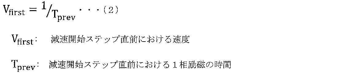
減速開始ステップ直前における1相励磁の時間を測定して、速度を式(2)で算出する。
更に、減速ステップ数と最終ステップ時間を指定して、ステップ間の平均速度の減少が一定になるように式(3)で算出する。
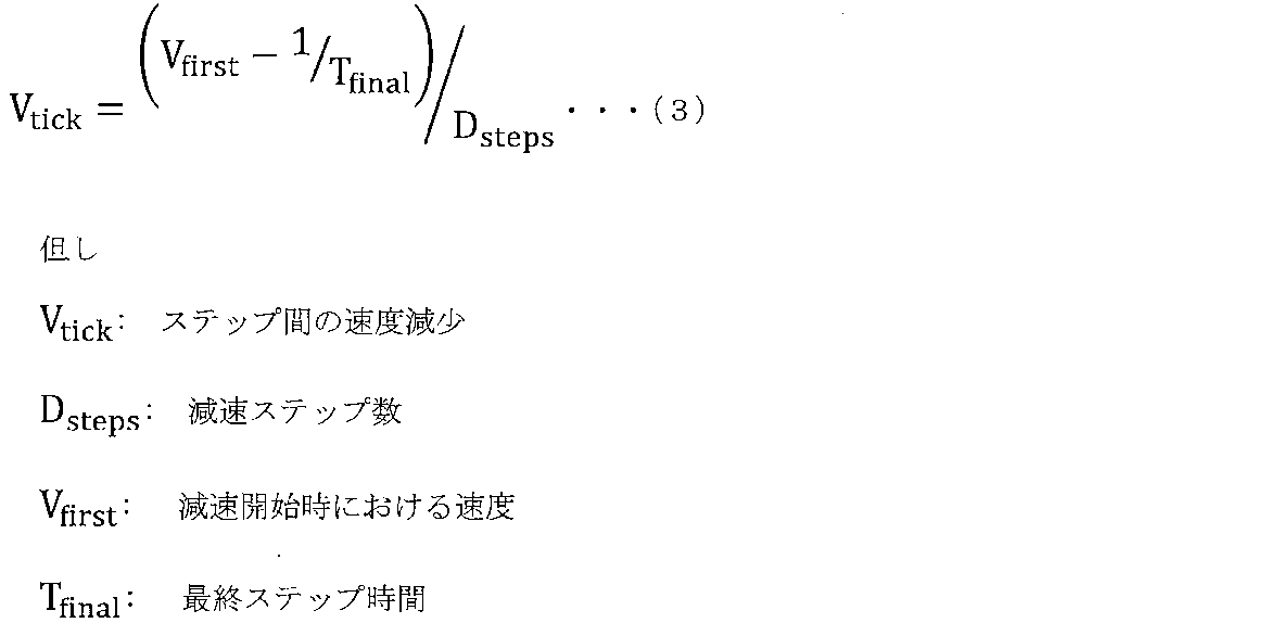
この速度減少を式(4)に代入すると、各ステップにおける速度が算出可能である。

この減速方式によれば、運動エネルギの主になる速度の指定により、効率的にオーバーランしない設定が可能である。
《最終速度指定+時間増加一定による減速制御方法》
各ステップの時間増加比率が一定になるように、減速ステップ数と最終ステップの時間を指定する方法である。この減速制御方法による速度と時間との関係を、図14に示す。
この減速制御方法では、減速開始直後の平均速度低下が大きく、減速終了直前の平均速度低下が小さいという特徴がある。
各ステップの時間増加比率が一定になるように、減速ステップ数と最終ステップの時間を指定する方法である。この減速制御方法による速度と時間との関係を、図14に示す。
この減速制御方法では、減速開始直後の平均速度低下が大きく、減速終了直前の平均速度低下が小さいという特徴がある。
《最終速度指定+減速度一定による減速制御方法》
減速度が一定になるように、減速ステップ数と最終ステップの速度を指定する方法である。このとき、速度は時間の一次関数になる。この減速制御方法による速度と時間との関係を、図15に示す。
《最終速度指定+速度テーブルによる減速制御方法》
減速開始ステップ直前の1相励磁の時間を測定し、減速ステップ数と最終ステップ時間を指定して、速度テーブル(台形・S字、直線部あり・なし)で比率計算した減速度で計算した速度から、転流時間を指定して減速する。この減速方法によれば、減速開始時直後と減速終了直前の速度が緩やかになり、負荷への影響が最も小さくなる。
減速度が一定になるように、減速ステップ数と最終ステップの速度を指定する方法である。このとき、速度は時間の一次関数になる。この減速制御方法による速度と時間との関係を、図15に示す。
《最終速度指定+速度テーブルによる減速制御方法》
減速開始ステップ直前の1相励磁の時間を測定し、減速ステップ数と最終ステップ時間を指定して、速度テーブル(台形・S字、直線部あり・なし)で比率計算した減速度で計算した速度から、転流時間を指定して減速する。この減速方法によれば、減速開始時直後と減速終了直前の速度が緩やかになり、負荷への影響が最も小さくなる。
上記の減速制御方法に加えて更に、1相励磁のPWM周期毎のデューティを意図的に徐々に下げるデューティ制御を併用することにより、モータ回転速度を減速してもよい。例えば、デューティを10%ずつ減らすことで、90%→80%→70%→60%になる。この場合、逆起電圧のゼロクロスをトリガに転流を行うと、例えば、モータの回転により負荷が増加する場合に、負荷の持ち上げ時に必要な電流が不足する可能性があるため、相切替(転流)時間を徐々に延ばす時間制御を併用するとよい。このデューティ制御による速度の減速への影響は、モータと電圧・負荷により異なる。
(本実施形態の効果)
(1) ステップ毎の転流時間の延長制御またはステップ間のゼロクロス間隔の延長制御を行うことにより、変動する電圧あるいはモータの回転により変動する負荷に対して、1相励磁かつ位置センサレスで駆動しているモータを停止させた際の停止位置精度を高めることができる。
(2) 本実施形態による減速制御方法によれば、モータの停止位置をオーバーランさせずに、所望の位置で停止させることができる。
(3) 本実施形態による減速制御方法によれば、駆動電圧あるいは負荷によらず、少ないステップ数かつ短時間で、モータの回転停止位置を正確に制御することができる。
(4) コイル電流が閾値を超過した場合、CPU101は、PWM周期で低速減衰モードを指定する。これにより、コイル電流の減衰を抑制でき、駆動力と保持力は維持できる。また、電磁ノイズの発生を抑制できる。
(5) コイル電流が閾値を超過した場合に、CPU101は、チャージモードと低速減衰モードとを繰り返すように制御する。これにより、電流リップルが小さくなる。
(1) ステップ毎の転流時間の延長制御またはステップ間のゼロクロス間隔の延長制御を行うことにより、変動する電圧あるいはモータの回転により変動する負荷に対して、1相励磁かつ位置センサレスで駆動しているモータを停止させた際の停止位置精度を高めることができる。
(2) 本実施形態による減速制御方法によれば、モータの停止位置をオーバーランさせずに、所望の位置で停止させることができる。
(3) 本実施形態による減速制御方法によれば、駆動電圧あるいは負荷によらず、少ないステップ数かつ短時間で、モータの回転停止位置を正確に制御することができる。
(4) コイル電流が閾値を超過した場合、CPU101は、PWM周期で低速減衰モードを指定する。これにより、コイル電流の減衰を抑制でき、駆動力と保持力は維持できる。また、電磁ノイズの発生を抑制できる。
(5) コイル電流が閾値を超過した場合に、CPU101は、チャージモードと低速減衰モードとを繰り返すように制御する。これにより、電流リップルが小さくなる。
(変形例)
本発明は、上記実施形態に限定されることなく、本発明の趣旨を逸脱しない範囲で、変更実施が可能であり、例えば、次の(a)~(c)のようなものがある。
(a) モータの種類は、ステッピングモータに限定されず、ブラシレスDCモータも含む。
(b) コイル電流がモータの駆動と最終的な位置保持に影響のない範囲で、オン・デューティを100%から徐々に減らして減速することも可能である。なお、オン・デューティとは、PWM周期毎のFETのオン時間のことをいう。
(c) CPU101は、停止制御タイマによらず、通電タイマに停止制御値を設定してステップ毎の転流時間の延長制御を行ってもよい。
本発明は、上記実施形態に限定されることなく、本発明の趣旨を逸脱しない範囲で、変更実施が可能であり、例えば、次の(a)~(c)のようなものがある。
(a) モータの種類は、ステッピングモータに限定されず、ブラシレスDCモータも含む。
(b) コイル電流がモータの駆動と最終的な位置保持に影響のない範囲で、オン・デューティを100%から徐々に減らして減速することも可能である。なお、オン・デューティとは、PWM周期毎のFETのオン時間のことをいう。
(c) CPU101は、停止制御タイマによらず、通電タイマに停止制御値を設定してステップ毎の転流時間の延長制御を行ってもよい。
100 モータ制御装置
101 CPU (制御手段の一例)
107 ブリッジ制御部
110 ブリッジ制御回路
113 PWM信号発生器
114 比較器
115 D/Aコンバータ
116 電流検出部 (電流検知手段の一例)
118 BEMF検出部 (ゼロクロス検知手段の一例)
120 ステッピングモータ
122XN,122XP,122YN,122YP 固定子
124,124X,124Y 固定子巻線 (モータコイルの一例)
126 回転子
130 上位装置
140 直流電源
142 アース線
20,20X,20Y Hブリッジ回路
2,4,6,8,15,17 FET
12,14,16,18 ダイオード
Icoil 電流測定値
Iref 電流基準値
VM モータ電圧
Mout0,Mout1,Mout2,Mout3 接続点
VMout0,VMout1,VMout2,VMout3 電圧
MVdd 電圧
IMout1-0,IMout3-2 コイル電流
101 CPU (制御手段の一例)
107 ブリッジ制御部
110 ブリッジ制御回路
113 PWM信号発生器
114 比較器
115 D/Aコンバータ
116 電流検出部 (電流検知手段の一例)
118 BEMF検出部 (ゼロクロス検知手段の一例)
120 ステッピングモータ
122XN,122XP,122YN,122YP 固定子
124,124X,124Y 固定子巻線 (モータコイルの一例)
126 回転子
130 上位装置
140 直流電源
142 アース線
20,20X,20Y Hブリッジ回路
2,4,6,8,15,17 FET
12,14,16,18 ダイオード
Icoil 電流測定値
Iref 電流基準値
VM モータ電圧
Mout0,Mout1,Mout2,Mout3 接続点
VMout0,VMout1,VMout2,VMout3 電圧
MVdd 電圧
IMout1-0,IMout3-2 コイル電流
Claims (8)
- モータに設けられたモータコイルの逆起電圧のゼロクロスを検知するゼロクロス検知手段と、
前記モータを1相励磁方式かつ位置センサレスで駆動制御し、前記ゼロクロス検知手段によって検知された前記逆起電圧のゼロクロスに基づいて転流し、駆動電圧と負荷に応じた回転速度によって前記モータの駆動制御を行うと共に、前記モータの駆動を停止する際には、算出された減速開始ステップから所望の位置で停止可能な所定回転速度以下に低下するまで、ステップ毎の転流時間の延長制御を行う制御手段と、
を備えるモータ駆動制御装置。 - 前記制御手段は、前記減速開始ステップから前記モータが前記所定回転速度以下になるまで、前記逆起電圧のゼロクロスに基づいた転流を中止して、前記ステップ毎の転流時間を長くする制御を行う、
ことを特徴とする請求項1に記載のモータ駆動制御装置。 - 前記制御手段は、前記ステップ毎の転流時間を一定の割合で増加させる、
ことを特徴とする請求項2に記載のモータ駆動制御装置。 - 前記減速開始ステップは、駆動ステップ数と減速ステップ数により算出される、
ことを特徴とする請求項1ないし3のうちいずれか1項に記載のモータ駆動制御装置。 - 前記モータコイルに接続されたハーフブリッジを組み合わせたHブリッジ回路と、
前記モータコイルに流れるモータ電流を検知する電流検知手段と、を備え、
前記制御手段は、前記減速開始ステップから停止するまでの間に、前記電流検知手段によって検知された前記モータ電流が所定の電流値を超過した場合、前記Hブリッジ回路に対して、PWM周期毎に低速減衰モードを指定する、
ことを特徴とする請求項1ないし4のうちいずれか1項に記載のモータ駆動制御装置。 - 前記制御手段は、電流制限時の動作モードとして、チャージモードと低速減衰モードとを繰り返させる制御を行う、
ことを特徴とする請求項5に記載のモータ駆動制御装置。 - 前記制御手段は、電流制限時の動作モードとして、PWM周期毎のチャージモードと低速減衰モードとの繰り返しの後、貫通防止モード、フライバック対応モード、フリーモードの順で遷移させる、
ことを特徴とする請求項6に記載のモータ駆動制御装置。 - モータに設けられたモータコイルの逆起電圧のゼロクロスを検知し、
前記モータを1相励磁方式かつ位置センサレスで駆動制御し、検知された前記逆起電圧のゼロクロスに基づいて転流し、駆動電圧と負荷に応じた回転速度によって前記モータの駆動制御を行うと共に、前記モータの駆動を停止する際には、算出された減速開始ステップから所望の位置で停止可能な所定回転速度以下に低下するまで、ステップ毎の転流時間の延長制御を行う、
ことを特徴とするモータ駆動制御方法。
Priority Applications (2)
| Application Number | Priority Date | Filing Date | Title |
|---|---|---|---|
| DE112017004395.6T DE112017004395T5 (de) | 2016-09-01 | 2017-08-09 | Motorantriebsteuervorrichtung und Motorantriebsteuerverfahren |
| US16/282,518 US10790768B2 (en) | 2016-09-01 | 2019-02-22 | Motor driving control device and motor driving control method |
Applications Claiming Priority (2)
| Application Number | Priority Date | Filing Date | Title |
|---|---|---|---|
| JP2016-171243 | 2016-09-01 | ||
| JP2016171243A JP6603638B2 (ja) | 2016-09-01 | 2016-09-01 | モータ駆動制御装置およびモータ駆動制御方法 |
Related Child Applications (1)
| Application Number | Title | Priority Date | Filing Date |
|---|---|---|---|
| US16/282,518 Continuation US10790768B2 (en) | 2016-09-01 | 2019-02-22 | Motor driving control device and motor driving control method |
Publications (1)
| Publication Number | Publication Date |
|---|---|
| WO2018043077A1 true WO2018043077A1 (ja) | 2018-03-08 |
Family
ID=61300944
Family Applications (1)
| Application Number | Title | Priority Date | Filing Date |
|---|---|---|---|
| PCT/JP2017/028892 Ceased WO2018043077A1 (ja) | 2016-09-01 | 2017-08-09 | モータ駆動制御装置およびモータ駆動制御方法 |
Country Status (4)
| Country | Link |
|---|---|
| US (1) | US10790768B2 (ja) |
| JP (1) | JP6603638B2 (ja) |
| DE (1) | DE112017004395T5 (ja) |
| WO (1) | WO2018043077A1 (ja) |
Cited By (1)
| Publication number | Priority date | Publication date | Assignee | Title |
|---|---|---|---|---|
| CN113763996A (zh) * | 2020-06-05 | 2021-12-07 | 株式会社东芝 | 磁盘装置 |
Families Citing this family (9)
| Publication number | Priority date | Publication date | Assignee | Title |
|---|---|---|---|---|
| JP7158910B2 (ja) | 2018-06-20 | 2022-10-24 | ミネベアミツミ株式会社 | ステッピングモータの制御装置及びステッピングモータの制御方法 |
| DE102018126954A1 (de) | 2018-10-29 | 2020-04-30 | Trinamic Motion Control Gmbh & Co. Kg | Verfahren und Schaltungsanordnung zur sensorlosen Lasterfassung bei Schrittmotoren |
| US10824130B2 (en) | 2019-01-31 | 2020-11-03 | Texas Instruments Incorporated | Stepper motor |
| GB2582612B (en) | 2019-03-28 | 2021-10-13 | Dyson Technology Ltd | A method of determining a position of a rotor of a brushless permanent magnet motor |
| JP7269824B2 (ja) * | 2019-08-07 | 2023-05-09 | ミネベアミツミ株式会社 | モータ駆動制御装置、モータユニット、およびモータ駆動制御方法 |
| CN112087171B (zh) * | 2020-08-26 | 2022-02-11 | 湖南英迈智能科技有限公司 | 电流平滑方法及装置 |
| JP7724702B2 (ja) * | 2021-12-03 | 2025-08-18 | ミネベアミツミ株式会社 | モータ駆動制御装置、モータユニット、およびモータ駆動制御方法 |
| DE102022107474A1 (de) | 2022-03-30 | 2023-10-05 | Audi Aktiengesellschaft | Endpositionserkennung von Aktuatoren |
| JP2023173629A (ja) * | 2022-05-26 | 2023-12-07 | ミネベアミツミ株式会社 | モータ駆動制御装置、モータユニット、およびモータ駆動制御方法 |
Citations (5)
| Publication number | Priority date | Publication date | Assignee | Title |
|---|---|---|---|---|
| US5793168A (en) * | 1996-08-23 | 1998-08-11 | Micro Linear Corporation | Active deceleration circuit for a brushless DC motor |
| JP2011139582A (ja) * | 2009-12-28 | 2011-07-14 | Sanyo Electric Co Ltd | モータ駆動回路 |
| US20120098473A1 (en) * | 2007-07-26 | 2012-04-26 | Radek Georgiev Nachev | Method for control of synchronous electrical motors |
| JP2013102656A (ja) * | 2011-11-10 | 2013-05-23 | Panasonic Corp | インバータ制御装置と電動圧縮機および電気機器 |
| US20140217939A1 (en) * | 2011-10-05 | 2014-08-07 | Sang-hyun Lee | Apparatus and method of decreasing speed of sensorless brush less direct current (bldc) motor |
Family Cites Families (2)
| Publication number | Priority date | Publication date | Assignee | Title |
|---|---|---|---|---|
| JP2005229743A (ja) | 2004-02-13 | 2005-08-25 | Mitsubishi Material Cmi Kk | ステッピングモータの制御方法 |
| CN106452224B (zh) * | 2016-10-31 | 2019-04-23 | 合肥杰发科技有限公司 | 用于电机的控制芯片、控制系统及控制方法 |
-
2016
- 2016-09-01 JP JP2016171243A patent/JP6603638B2/ja active Active
-
2017
- 2017-08-09 WO PCT/JP2017/028892 patent/WO2018043077A1/ja not_active Ceased
- 2017-08-09 DE DE112017004395.6T patent/DE112017004395T5/de active Pending
-
2019
- 2019-02-22 US US16/282,518 patent/US10790768B2/en active Active
Patent Citations (5)
| Publication number | Priority date | Publication date | Assignee | Title |
|---|---|---|---|---|
| US5793168A (en) * | 1996-08-23 | 1998-08-11 | Micro Linear Corporation | Active deceleration circuit for a brushless DC motor |
| US20120098473A1 (en) * | 2007-07-26 | 2012-04-26 | Radek Georgiev Nachev | Method for control of synchronous electrical motors |
| JP2011139582A (ja) * | 2009-12-28 | 2011-07-14 | Sanyo Electric Co Ltd | モータ駆動回路 |
| US20140217939A1 (en) * | 2011-10-05 | 2014-08-07 | Sang-hyun Lee | Apparatus and method of decreasing speed of sensorless brush less direct current (bldc) motor |
| JP2013102656A (ja) * | 2011-11-10 | 2013-05-23 | Panasonic Corp | インバータ制御装置と電動圧縮機および電気機器 |
Cited By (2)
| Publication number | Priority date | Publication date | Assignee | Title |
|---|---|---|---|---|
| CN113763996A (zh) * | 2020-06-05 | 2021-12-07 | 株式会社东芝 | 磁盘装置 |
| CN113763996B (zh) * | 2020-06-05 | 2023-03-31 | 株式会社东芝 | 磁盘装置 |
Also Published As
| Publication number | Publication date |
|---|---|
| JP6603638B2 (ja) | 2019-11-06 |
| DE112017004395T5 (de) | 2019-05-16 |
| JP2018038213A (ja) | 2018-03-08 |
| US20190190415A1 (en) | 2019-06-20 |
| US10790768B2 (en) | 2020-09-29 |
Similar Documents
| Publication | Publication Date | Title |
|---|---|---|
| JP6603638B2 (ja) | モータ駆動制御装置およびモータ駆動制御方法 | |
| US7847498B2 (en) | Brushless motor driving device, brushless motor starting method, and method of detecting rotor stop position of brushless motor | |
| US9093931B2 (en) | Driving apparatus and stop position detection method | |
| US11114962B2 (en) | Semiconductor device, motor drive system, and motor control program | |
| JP6272798B2 (ja) | モータ駆動制御装置およびモータ駆動制御方法 | |
| JP6322134B2 (ja) | モータ制御装置およびモータ制御方法 | |
| US11005400B2 (en) | Motor current control device and motor current control method | |
| CN105191113A (zh) | 用于无刷电机的ac/ac变换器 | |
| JP2015109792A (ja) | Bldcモータにおける相電流調整 | |
| WO2018088442A1 (ja) | 電動機の界磁位置検出方法 | |
| JP2011211799A (ja) | モータ駆動装置 | |
| CN105827164A (zh) | 电机电流控制装置以及电机电流控制方法 | |
| KR102619910B1 (ko) | 상전압 검출을 이용한 브러시리스 직류모터 기동 제어방법 및 장치 | |
| CN105453410A (zh) | 控制装置和使用该控制装置的交流电动机系统 | |
| JP2010088267A (ja) | ブラシレスモータの制御装置及び制御方法 | |
| CN115398794B (zh) | 马达控制装置、马达系统及马达控制方法 | |
| JP2011125079A (ja) | ブラシレスモータの駆動装置、及びブラシレスモータの始動方法 | |
| JP2017131000A (ja) | 3相ブラシレスモータのセンサレス駆動方法 | |
| CN108075691A (zh) | 控制多相无刷直流电机的控制器和方法及自动同步系统 | |
| US11942890B2 (en) | Semiconductor device, motor drive system, and method of starting motor | |
| US20190379309A1 (en) | Brushless dc motor control method and control device | |
| JP6173107B2 (ja) | ブラシレスモータの駆動装置、及び駆動方法 | |
| JP5087411B2 (ja) | モータ駆動装置 | |
| CN112313872B (zh) | 步进电机的控制装置及步进电机的控制方法 | |
| EP2704308A1 (en) | Brushless motor control device and brushless motor control method |
Legal Events
| Date | Code | Title | Description |
|---|---|---|---|
| 121 | Ep: the epo has been informed by wipo that ep was designated in this application |
Ref document number: 17846086 Country of ref document: EP Kind code of ref document: A1 |
|
| 122 | Ep: pct application non-entry in european phase |
Ref document number: 17846086 Country of ref document: EP Kind code of ref document: A1 |