WO2018042732A1 - 磁気トンネル接合素子およびその製造方法 - Google Patents
磁気トンネル接合素子およびその製造方法 Download PDFInfo
- Publication number
- WO2018042732A1 WO2018042732A1 PCT/JP2017/011263 JP2017011263W WO2018042732A1 WO 2018042732 A1 WO2018042732 A1 WO 2018042732A1 JP 2017011263 W JP2017011263 W JP 2017011263W WO 2018042732 A1 WO2018042732 A1 WO 2018042732A1
- Authority
- WO
- WIPO (PCT)
- Prior art keywords
- layer
- magnetic
- tunnel junction
- magnetic tunnel
- layer made
- Prior art date
- Legal status (The legal status is an assumption and is not a legal conclusion. Google has not performed a legal analysis and makes no representation as to the accuracy of the status listed.)
- Ceased
Links
Images





Classifications
-
- H—ELECTRICITY
- H10—SEMICONDUCTOR DEVICES; ELECTRIC SOLID-STATE DEVICES NOT OTHERWISE PROVIDED FOR
- H10N—ELECTRIC SOLID-STATE DEVICES NOT OTHERWISE PROVIDED FOR
- H10N50/00—Galvanomagnetic devices
- H10N50/01—Manufacture or treatment
-
- H—ELECTRICITY
- H10—SEMICONDUCTOR DEVICES; ELECTRIC SOLID-STATE DEVICES NOT OTHERWISE PROVIDED FOR
- H10N—ELECTRIC SOLID-STATE DEVICES NOT OTHERWISE PROVIDED FOR
- H10N50/00—Galvanomagnetic devices
- H10N50/10—Magnetoresistive devices
-
- H—ELECTRICITY
- H10—SEMICONDUCTOR DEVICES; ELECTRIC SOLID-STATE DEVICES NOT OTHERWISE PROVIDED FOR
- H10N—ELECTRIC SOLID-STATE DEVICES NOT OTHERWISE PROVIDED FOR
- H10N50/00—Galvanomagnetic devices
- H10N50/80—Constructional details
-
- H—ELECTRICITY
- H10—SEMICONDUCTOR DEVICES; ELECTRIC SOLID-STATE DEVICES NOT OTHERWISE PROVIDED FOR
- H10N—ELECTRIC SOLID-STATE DEVICES NOT OTHERWISE PROVIDED FOR
- H10N50/00—Galvanomagnetic devices
- H10N50/80—Constructional details
- H10N50/85—Materials of the active region
-
- H—ELECTRICITY
- H10—SEMICONDUCTOR DEVICES; ELECTRIC SOLID-STATE DEVICES NOT OTHERWISE PROVIDED FOR
- H10B—ELECTRONIC MEMORY DEVICES
- H10B61/00—Magnetic memory devices, e.g. magnetoresistive RAM [MRAM] devices
Definitions
- the present invention relates to a magnetic tunnel junction element and a manufacturing method thereof.
- Magnetization reversal using spin transfer torque (hereinafter referred to as “STT”) is suitable for memory devices with high density and low power consumption because the current value required for writing decreases as the device size decreases. Yes.
- STT-MRAM magnetic memory
- the magnetic memory using magnetization reversal by STT is composed of a magnetic tunnel junction (MTJ) element (hereinafter also referred to as “MTJ element”).
- MTJ element has a configuration in which a tunnel barrier layer (tunnel insulating film) is sandwiched between a reference (fixed) layer whose magnetization direction is fixed and a recording (free) layer whose magnetization direction changes. .
- the performance of the MTJ element is expressed by a tunnel magnetoresistance ratio (TMR ratio), thermal stability, and threshold current.
- the tunnel magnetoresistance ratio is (R ap ⁇ R p ) / R p (where R p is the resistance value when the magnetization of the reference layer adjacent to the barrier layer and the magnetization of the recording layer are arranged in parallel, R ap : Resistance value when the magnetization of the reference layer adjacent to the barrier layer and the magnetization of the recording layer are arranged in antiparallel.
- the thermal stability is K eff ⁇ V / k B T (where K eff is the effective magnetic anisotropy energy density of the recording layer, V is the volume of the recording layer, k B is the Boltzmann constant, and T is the absolute temperature. ).
- the MTJ element has a larger tunnel magnetoresistance ratio, and the larger the value obtained by dividing the thermal stability by the threshold current, the more suitable.
- the magnetization direction is the same when the magnetization is reversed by STT and when the thermal reversal occurs.
- the magnetization passes in different directions when the magnetization is reversed by STT and when the thermal reversal occurs.
- the magnetization passes through the perpendicular direction with a large demagnetizing field
- the thermal reversal the magnetization passes in an in-plane direction with a small demagnetizing field.
- the ratio of thermal stability to the threshold current is smaller than that in the perpendicular magnetization type. For this reason, recently, a perpendicular magnetization type MTJ element has attracted more attention, and a perpendicular magnetization type MTJ element has come to be used.
- a perpendicular magnetization type MTJ element As such a perpendicular magnetization type MTJ element, a device having a high tunnel magnetoresistance ratio, a high thermal stability, and a low threshold current has been developed by using a ferromagnetic layer made of CoFeB and an MgO insulating film. (For example, refer to Patent Document 1), and studies using this material system are being actively conducted.
- the recording layer (CoFeB) is replaced with an oxygen-containing barrier layer (MgO) like a MgO (barrier layer) / CoFeB (recording layer) / MgO (protective layer) structure.
- MgO oxygen-containing barrier layer
- Those having a structure (double interface structure) sandwiched between protective layers (MgO) have also been developed (see, for example, Patent Document 1).
- those having a double interface structure using a conductive oxide layer as a protective layer and those having a metal cap layer disposed on the protective layer have been developed (see, for example, Patent Document 2).
- the MTJ element having such a double interface structure has a higher recording performance than a tunnel junction element having no MgO protective layer due to two perpendicular magnetic anisotropies generated at the CoFeB / MgO interface below the recording layer and above the recording layer.
- the film thickness of the layer can be increased. Since the thermal stability increases in proportion to the thickness of the recording layer, the thermal stability can be improved by increasing the thickness. At the same time, the damping constant ⁇ of the recording layer can be reduced by increasing the film thickness of the recording layer. Since the value of the write current is proportional to the damping constant ⁇ , the value of the write current can be reduced at the same time. As a result, the MTJ element having the double interface structure has a high thermal stability and a small write current, that is, a large value obtained by dividing the thermal stability by the threshold current.
- a protective layer such as Ta is laminated on the recording layer instead of the MgO protective layer.
- Ta absorbs boron by heat treatment, CoFeB is crystallized and a high TMR ratio is obtained.
- the MTJ element having the double interface structure described in Patent Documents 1 and 2 has CoFeB sandwiched between MgO and has no cap of Ta or the like, so that boron does not easily diffuse due to heat treatment. For this reason, there was a problem that CoFeB was not crystallized by the heat treatment and the TMR ratio was lowered.
- an MTJ element in which a thin nonmagnetic layer such as Ta is inserted between recording layers has been proposed (for example, see Non-Patent Document 1).
- a non-magnetic layer such as Ta absorbs boron by heat treatment, and CoFeB is crystallized, so that a high TMR ratio is obtained.
- a CoFeB reference layer was stacked on a film with high perpendicular magnetic anisotropy such as a [Co / Pt] multilayer film as a magnetization fixed layer with a thin Ta of about 4 mm called a magnetic coupling layer sandwiched therebetween.
- MTJ has been proposed (see, for example, Non-Patent Document 1).
- a CoFeB / MgO / CoFeB tunnel junction a high TMR ratio is obtained when CoFeB and MgO are (001) -oriented.
- [Co / Pt] has an (111) crystal orientation of fcc
- CoFeB is crystal-oriented in the fcc crystal direction of [Co / Pt], resulting in a high TMR ratio. I can't get it.
- the magnetic coupling layer is used to obtain a high TMR ratio by orienting CoFeB in the (001) direction by once cutting the crystal orientation of [Co / Pt].
- the actual structure of the magnetic tunnel junction element is that a lower electrode layer 28 and a base layer 29 are formed on a substrate 27, and a fixed layer 25, magnetic coupling is formed on the base layer 29.
- the layer 26, the reference layer 11, the barrier layer 12, the recording layer 13, the protective layer 14, and the upper electrode layer 30 are stacked in this order.
- a Co alloy-based perpendicular magnetic film such as Co / Pt is often used as will be described later.
- this Co alloy film In order for this Co alloy film to have perpendicular magnetic anisotropy, it is necessary that the (0001) direction, which is the easy axis of magnetization of the hcp structure, be a polycrystalline alignment film perpendicular to the substrate.
- a method for orienting the Co alloy film in this manner a method of growing heteroepitaxially on the underlying layer is used.
- a Co alloy film is formed thereon.
- a polycrystalline orientation film having a (0001) plane parallel to the underlayer grows.
- a Ti, Sc, Ru, and Hf film having an hcp structure a Pt, Pd, Au, and Cu film having an fcc structure are often used.
- the present invention has been made paying attention to this problem, and provides a method for manufacturing a magnetic tunnel junction element that improves the heat resistance and the TMR ratio and solves this problem, and a magnetic tunnel junction element generated by the manufacturing method.
- the purpose is to do.
- the method of manufacturing a magnetic tunnel junction device according to the present invention utilizes a so-called “plasma treatment” (hereinafter referred to as “PT” for short), which is sputter etching of a metal surface. .
- PT plasma treatment
- a reference layer, a magnetic coupling layer made of a non-magnetic material, an underlayer made of a metal material, and a fixed layer made of a ferromagnetic material and having a fixed magnetization direction were laminated to form a magnetic tunnel junction device.
- a fixed layer is formed and laminated after the surface of the underlayer is subjected to plasma treatment.
- the present invention forms a fixed layer composed of a [Co / Pt] multilayer after forming a Pt underlayer, which is an underlayer of the magnetic tunnel junction element, and plasma-treating the Pt surface with Ar or the like.
- the smoothness of the Pt surface and the crystal orientation of the fixed layer made of a [Co / Pt] multilayer film are improved, and the heat resistance and TMR ratio of the magnetic tunnel junction element can be improved.
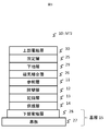
- FIG. 1 is a diagram showing a typical configuration example (first configuration example) of a laminated structure of magnetic tunnel junction elements (MTJ elements) according to the present invention.
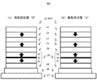
- FIG. 2 is an explanatory diagram showing a laminated structure of a magnetic tunnel junction device according to the present invention, and (a) a low resistance state and (b) a high resistance state.
- FIG. 3 is a diagram showing a second configuration example of the laminated structure of the magnetic tunnel junction element according to the present invention.
- FIG. 4 is a diagram showing a third configuration example of the laminated structure of the magnetic tunnel junction element according to the present invention.
- FIG. 5 is a diagram showing the results of measuring the average surface roughness (Ra) of the Pt surface.
- FIG. 1 is a diagram showing a typical configuration example (first configuration example) of a laminated structure of magnetic tunnel junction elements (MTJ elements) according to the present invention.
- FIG. 2 is an explanatory diagram showing a laminated structure of a magnetic tunnel junction device according to the present invention,
- FIG. 6 is a diagram showing the measurement result of the average surface roughness (Ra) of the Co / Pt surface with and without PT.
- FIG. 7 is a diagram showing measured values of the anisotropy magnetic field Hk immediately after film formation and the heat treatment depending on the presence or absence of PT.
- FIG. 8 is a simplified diagram of a method for manufacturing a magnetic tunnel junction device according to an embodiment of the present invention.
- FIG. 9 is a diagram showing changes in measured values of the TMR ratio and the junction resistance (RA) depending on the presence or absence of PT.
- FIG. 10 is a diagram showing the relationship between the amount of cutting by PT and the TMR ratio.
- FIG. 11 is a diagram showing the results of EDX ray analysis performed on the element Fe with respect to the stacked structure of the MTJ element.
- FIG. 12 is a diagram obtained by imaging a [Co / Pt] grain boundary with a TEM as a cross section of the fixed layer.
- FIG. 13 is a diagram in which the cross section of [Co / Pt] of the fixed layer and the Pt base therebelow is imaged by TEM.
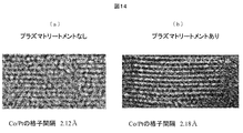
- FIG. 14 is an enlarged view of the [Co / Pt] portion of the fixed layer in the TEM image of FIG.
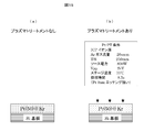
- FIG. 15 is a schematic diagram showing the presence / absence of plasma treatment (PT) using Ar on the Pt base.
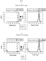
- FIG. 16 is a diagram showing measurement results by HR-RBS analysis.
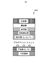
- FIG. 1 is a diagram showing a typical configuration example (first configuration example) of a laminated structure of a magnetic tunnel junction (MTJ) element according to the present invention.
- the magnetic tunnel junction element 10 has a structure in which a reference layer 11, a barrier layer 12, a recording layer 13, and a protective layer 14 are laminated in this order, and a base layer 15 for forming these layers by sputtering or the like. Yes.
- the magnetic tunnel junction element 10 is formed with a lower electrode layer 28 and a base layer 29 on a substrate 27 as shown in the figure, and on the base layer 29, a fixed layer 25 and a magnetic coupling layer 26.
- the reference layer 11, the barrier layer 12, the recording layer 13, the protective layer 14, and the upper electrode layer 30 are stacked in this order. In this case, each layer can be formed on the substrate 27 and then heat-treated.
- the substrate 27, the lower electrode layer 28, the base layer 29, the fixed layer 25, and the magnetic coupling layer 26 form the base layer 15.
- the fixed layer 25 constituting the base layer 15 is a ferromagnetic material, and the magnetization direction is fixed in the direction perpendicular to the film surface.
- the magnetic coupling layer 26 constituting the base layer 15 is a non-magnetic material and is made of, for example, a Ta film having a thickness of 0.4 nm. Other than Ta, a film made of at least one of Hf, W, Mo, Nb, Zr, Y, Sc, Ti, V, and Cr may be used.
- the reference layer 11 is a ferromagnetic material, and has a magnetization direction fixed in a direction perpendicular to the film surface, and is made of, for example, a CoFeB film having a thickness of 1.0 to 1.2 nm.
- the barrier layer 12 is a nonmagnetic material containing oxygen, and is made of, for example, a MgO film having a thickness of 1.0 to 1.3 nm.
- oxygen is not limited.
- the recording layer 13 is a ferromagnetic material, and the magnetization direction is variable in a direction perpendicular to the film surface.
- the first ferromagnetic layer and an insertion layer made of a non-magnetic material are used.
- the first ferromagnetic layer and the second ferromagnetic layer are magnetically coupled via the insertion layer.
- the first ferromagnetic layer has a magnetization direction that is variable in a direction perpendicular to the film surface, and is made of, for example, a CoFeB film having a thickness of 1.4 to 1.5 nm.
- the insertion layer is made of a nonmagnetic material, for example, a Ta or W film having a thickness of 0.2 to 0.5 nm.
- the second ferromagnetic layer has a magnetization direction that is variable in a direction perpendicular to the film surface, and is made of, for example, a CoFeB film having a thickness of 1.0 to 1.5 nm.
- the protective layer 14 is a nonmagnetic material containing oxygen, and is made of, for example, a MgO layer having a thickness of 1.0 to 1.1 nm. However, the inclusion of oxygen as a nonmagnetic material is not limited.
- the protective layer 14 may be made of a conductive oxide film.
- the base layer 15 includes the fixed layer 25 and the magnetic coupling layer 26, and the base layer 15 is disposed on the surface of the reference layer 11 opposite to the barrier layer 12 side.
- the fixed layer 25 includes a third ferromagnetic layer 31, a fourth ferromagnetic layer 32, and a nonmagnetic layer 33 sandwiched between both.
- the third ferromagnetic layer 31 is formed by laminating a Co film having a thickness of 0.5 nm and a Pt film having a thickness of 0.3 nm alternately four times, and then laminating a Co film having a thickness of 0.5 nm. Made of film.
- the fourth ferromagnetic layer 32 is formed by laminating a Co film having a thickness of 0.5 nm and a Pt film having a thickness of 0.3 nm alternately two times, and then laminating a Co film having a thickness of 0.5 nm. Made of film.
- the magnetic coupling layer 26 is a nonmagnetic material and is sandwiched between the fixed layer 25 and the reference layer 11 and is made of, for example, a Ta film having a thickness of 0.4 nm.
- the fixed layer 25 is provided so that the fourth ferromagnetic layer 32 is in contact with the magnetic coupling layer 26.
- the reference layer 11 is magnetically coupled to the fixed layer 25 via the magnetic coupling layer 26, and the magnetization direction is fixed in one direction perpendicular to the film surface.
- the magnetic tunnel junction element 10 a magnetic tunnel junction is generated between the reference layer 11 and the recording layer 13 via the barrier layer 12. Further, as shown in FIG. 1, the magnetic tunnel junction element 10 has a double interface structure in which the recording layer 13 is sandwiched between the barrier layer 12 and the protective layer 14, and the interface between the recording layer 13 and the barrier layer 12; In addition, perpendicular magnetic anisotropy occurs at the interface between the recording layer 13 and the protective layer 14, and the magnetization direction of the recording layer 13 is perpendicular to the film surface. Further, in the magnetic tunnel junction element 10, the magnetization direction of the recording layer 13 is changed by spin injection magnetization reversal.
- the reference layer 11, the barrier layer 12, the recording layer 13, and the protective layer 14 are sequentially formed on the base layer 15, and then heat treatment is performed.
- heat treatment is performed as a method for depositing each layer.
- sputtering such as physical vapor deposition or molecular beam epitaxial growth (MBE) can be used.
- the heat treatment temperature is preferably 350 ° C. to 450 ° C.
- the substrate 27 has a configuration including transistors and multilayer wiring layers.
- the lower electrode layer 28 is, for example, a conductive layer having a thickness of about 20 to 50 nm, and is made of a metal material such as Ta, TaN, Ti, TiN, Cu, CuN, Au, Ag, and Ru, or an alloy thereof. .
- the lower electrode layer 28 may have a structure in which a plurality of metal materials are stacked, for example, a structure of Ta / Ru / Ta.
- the lower electrode layer 28 is a layer serving as a base for forming each of the upper layers, and has a flat surface formed by chemical mechanical polishing (CMP), gas cluster ion beam (GCIB), or the like after film formation. .
- CMP chemical mechanical polishing
- GCIB gas cluster ion beam
- the underlayer 29 is made of, for example, a Pt film having a thickness of about 5 nm, but may be made of a metal material such as Ti, Sc, Pd, Ru, Cu, Au, and Hf in addition to Pt. .
- the upper electrode layer 30 is, for example, a conductive layer having a thickness of about 10 to 100 nm, and is made of a metal material such as Ta, TaN, Ti, TiN, Cu, CuN, Au, Ag, and Ru, or an alloy thereof. .
- the upper electrode layer 30 may have a structure in which a plurality of metal materials are stacked, for example, a structure such as Ta / Ru.
- FIG. 3 shows a second configuration example of the laminated structure of the magnetic tunnel junction element 10.
- the layers from the fixed layer 25 to the protective layer 14 shown in FIG. 1 are turned over to form a laminated structure as shown in FIG. 3, and an underlayer 29 is inserted between the magnetic coupling layer 26 and the fixed layer 25.
- the protective layer 14 and the lower electrode layer 28 are in contact with each other, and the fixed layer 25 and the upper electrode layer 30 are in contact with each other.
- the substrate 27 and the lower electrode layer 28 form the base layer 15.
- a thin magnetic film may be inserted between the magnetic coupling layer 26 and the underlayer 29 in order to strengthen the magnetic coupling between the reference layer 11 and the fixed layer 25.
- FIG. 4 shows a third configuration example of the laminated structure of the magnetic tunnel junction element 10.
- the second barrier layer 12a, the second reference layer 11a, and the second layer are arranged between the recording layer 13 and the protective layer 14 in this order from the recording layer 13 side.
- the magnetic coupling layer 26a, the second underlayer 29a, and the second pinned layer 25a are stacked.
- five layers from the substrate 27 to the magnetic coupling layer 26 form the base layer 15.
- a thin magnetic film may be inserted in order to strengthen the magnetic coupling between the second magnetic coupling layer 26a and the second underlayer 29a.
- the surface of the underlayer is sputter etched after forming the underlayer, so-called plasma treatment (hereinafter referred to as “PT”).
- PT plasma treatment
- the fixed layer includes a Co alloy such as the Co / Pt laminated film, the Co / Pd laminated film, the Co / Ni laminated film, the CoPt alloy film, the CoCrPt alloy film, and the CoCrRu alloy film.
- a perpendicular magnetic film of the system is used. Therefore, in order for this Co alloy film to have perpendicular magnetic anisotropy, as described above, it is necessary that the (0001) direction, which is the easy axis of magnetization of the hcp structure, be a polycrystalline alignment film perpendicular to the substrate.
- a method is used in which a Co alloy film is grown heteroepitaxially on the underlying layer. That is, when a (0001) orientation film having an hcp structure or an (111) orientation film having an fcc structure having an arrangement similar to the atomic arrangement of the closest dense surface of the hcp structure is used as a base layer, a Co alloy is formed thereon.
- the alloy film is affected by the crystal orientation of the underlayer, and a polycrystalline orientation film having a (0001) plane parallel to the underlayer grows.
- the above-mentioned metal materials Pt, Ti, Sc, Pd, Ru, Cu, Au, Hf, etc.
- Ti, Sc, Ru and Hf have an hcp structure
- Pt, Pd, Cu and Au have an fcc structure.
- FIG. 5 shows the results of measuring the average surface roughness (Ra) of the Pt surface in the presence / absence of PT.
- FIG. 5 (a) shows the measurement result when PT is not applied to the Pt base
- FIG. 5 (b) shows that PT is present (Pt having a thickness of 8 nm becomes 5 nm by PT treatment, and no PT is present).
- the measurement result in the case of the same state as the case) is shown.
- Ra 0.219 nm without PT
- FIG. 6 shows the measurement result of the average surface roughness (Ra) of the Co / Pt surface depending on whether or not PT is applied to the Pt base in this case.
- FIG. 6 (a) shows the measurement result without PT
- FIG. 6 (b) shows with PT (similar to FIG. 5, Pt with a thickness of 8 nm becomes 5 nm with PT treatment, and without PT).
- the measurement result in the case of the same state as the case) is shown.
- Ra 0.241 nm
- Ra 0.181 nm.
- Co / Pt may be smoothed by performing PT on the Pt base. I understood.
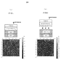
- FIG. 7 shows a state in which a thickness of 3 nm (corresponding to the nonmagnetic layer 33) is laminated on the laminated structure shown in FIG.
- the comparison result of the measured value of the anisotropic magnetic field Hk at the time of heat-treating for 1 hour is shown.
- 7A shows a laminated structure without PT
- FIG. 7B shows a laminated structure with PT
- FIG. 7C shows measured values of the anisotropic magnetic field Hk with / without PT.
- a graph is shown.
- FIG. 8 is a simplified diagram of a method for manufacturing a magnetic tunnel junction device according to an embodiment of the present invention.
- the Pt surface is subjected to plasma treatment (PT) with a rare gas such as Ar, Kr and Xe after forming the underlying layer (for example, Pt), Subsequently, a fixed layer made of, for example, [Co / Pt] is formed.
- PT plasma treatment
- a rare gas such as Ar, Kr and Xe
- a fixed layer made of, for example, [Co / Pt] is formed.
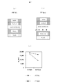
- FIG. 9 is a graph (graph) showing changes in measured values of the TMR ratio and junction resistance (RA) in the laminated structure of the magnetic tunnel junction element described above in the presence / absence of PT with respect to the Pt base. It is.
- FIG. 9A shows the laminated structure of the magnetic tunnel junction element used in the actual measurement
- FIG. 9B shows the measurement of TMR ratio and junction resistance (RA) with and without PT.
- a graph of values is shown.
- FIG. 9A simply shows a case where “Pt (5)” without PT, and “Pt (8 ⁇ 5)” with PT, which are written on the underlayer (ie, FIG. 9). Same as 5-7).
- RA Resistance-Area product
- the TMR ratio increased by about 20% in the case with PT than in the case without PT, and the resistance value (RA) was found to be slightly decreased but not greatly changed. . That is, by performing PT on the Pt base, it is possible to improve the TMR ratio characteristics, and hence the magnetic characteristics.
- FIG. 10 is a graph (graph) showing the relationship between the amount of scraping by PT and the TMR ratio with respect to the Pt underlayer in the laminated structure of the magnetic tunnel junction element described above.
- FIG. 10 (a) shows the laminated structure of the magnetic tunnel junction element used in the actual measurement
- FIG. 10 (b) is a graph showing the characteristics of the TMR ratio from the absence of PT to the Pt scraping amount of 6 nm by PT. Show. It can be seen that the TMR ratio tends to decrease with a peak at a scraping amount of about 3 nm, whether the cutting amount is small or large. That is, if the cutting amount is increased, the characteristics of the TMR ratio are not improved, and an appropriate cutting amount exists.
- FIG. 11 is a graph (graph) showing the result of performing EDX ray (energy dispersive X-ray) analysis on the laminated structure of the magnetic tunnel junction element with respect to the element Fe in the presence / absence of PT with respect to the Pt base. is there.
- FIG. 11A shows the characteristics when no PT is provided
- FIG. 11B shows the characteristics when PT is provided.
- whether or not to perform plasma treatment (PT) on the Pt (Pt base) constituting the base layer is formed from the right base layer (with / without PT).
- FIG. 12 is a diagram obtained by imaging a cross section of a magnetic tunnel junction element with a TEM when heat treatment (annealing) is performed at 400 ° C. for 1 hour.
- FIG. 12A is an imaging diagram of a sample without PT
- FIG. 12B is an imaging diagram of a sample with PT.
- the particle size of [Co / Pt] is about 13 nm in the sample without PT, but is estimated to be about 20 nm in the sample with PT.
- the grain size is increased in this manner, it is presumed that the roughness is reduced and the perpendicular magnetic anisotropy is increased. Further, since the grain size is decreased by increasing the grain size, the diffusion of Fe element through the crystal grain boundary is suppressed.
- FIG. 13 and FIG. 14 show that when heat treatment (annealing) is performed at 400 ° C. for 1 hour, from [Co / Pt] of the fixed layer to Pt of the underlying layer below it and TaN of the lower electrode below It is the figure which imaged the cross section with TEM.
- (a) is an imaging diagram of a sample without PT
- (b) in FIGS. 13 and 14 is an imaging diagram of a sample with PT.
- FIG. 14 is an enlarged view of the [Co / Pt] portion.
- the lattice spacing of Pt is about 2.29 mm
- the lattice spacing of [Co / Pt] is about 2.12 mm.
- the lattice spacing of Pt is about 2.31 cm
- the lattice spacing of [Co / Pt] is about 2.18 cm. Comparing the figures, it can be observed that the crystal orientation and the lattice spacing change depending on the presence or absence of PT. Regarding [Co / Pt] of the fixed layer, as is apparent from FIG. 14, it can be observed that the crystal lattice fringes of [Co / Pt] are aligned with PT. That is, it was confirmed that the crystal orientation of [Co / Pt] was improved.
- FIG. 15 is a schematic diagram showing the presence / absence of plasma treatment (PT) using Ar for the Pt base for comparison by HR-RBS analysis.
- A No PT,
- b PT, and the Pt-PT conditions are as shown.
- a Pt film with a thickness of 50 nm was formed on a silicon (Si) substrate with Kr gas, and plasma treatment (PT) was performed on the surface in situ after the film formation. Thereafter, the sample was subjected to HR-RBS analysis to evaluate the Ar implantation depth and implantation amount.
- FIG. 16 is a diagram showing the measurement results by the above HR-RBS analysis, where (a) is without PT and (b) is with PT. In both figures, a graph in which the atomic percent (at%) on the vertical axis is enlarged is shown (maximum value is enlarged from 100% to 5%). As shown in (b), Ar was detected in the range from the Pt surface to 10 nm in the sample subjected to PT. Further, Ar on the surface of the silicon (Si) substrate is implanted at the time of substrate cleaning before film formation. In addition, although the graph line type of Kr is described in the figure, since it was below the detection lower limit by measurement, it does not appear in the figure.
- the magnetic tunnel junction element according to the present invention can employ various crystalline magnetic films in addition to the Co alloy-based perpendicular magnetic film as the fixed layer.
- an FePt perpendicular magnetic film can be used.
- FePt alloys are L1 0 type ordered alloy, the magnetization direction perpendicular to the substrate, it is necessary to crystal orientation of the crystal c axis perpendicular to the film surface.
- crystal structure of such a base film for crystal orientation those having an NaCl structure, an fcc structure, and a bcc structure are often used.
- a MgO film having an NaCl structure, a CrRu alloy film having an fcc crystal structure, and a Cr / Ta, Cr / MgO laminated film having a bcc crystal structure are often used as the base film.
- a SmCo 5 type perpendicular magnetic film can also be used.
- the crystal c-axis needs to be oriented in the direction perpendicular to the film surface.
- those having an fcc structure are used.
- a Cu, Cu / Ti laminated film having an fcc crystal structure is often used.
- the applicability of the magnetic tunnel junction device according to the present invention is applicable not only to STT devices but also to 3-terminal SOT (Spin Orbit Torque) devices.
Landscapes
- Engineering & Computer Science (AREA)
- Manufacturing & Machinery (AREA)
- Mram Or Spin Memory Techniques (AREA)
- Hall/Mr Elements (AREA)
Abstract
よりTMR比が高く、耐熱性の高い磁気トンネル接合素子およびその製造方法を提供するために、積層順に、金属材料から成る下地層、強磁性体から成り磁化方向が固定である固定層、非磁性体から成る磁気結合層、強磁性体から成り磁化方向が固定である参照層、非磁性体から成る障壁層および強磁性体から成る記録層を積層して、または、積層順に、強磁性体から成る記録層、非磁性体から成る障壁層、強磁性体から成り磁化方向が固定である参照層、非磁性体から成る磁気結合層、金属材料から成る下地層および強磁性体から成り磁化方向が固定である固定層を積層して、磁気トンネル接合素子を構成するに際して、成膜した下地層の表面をプラズマトリートメントにした後に固定層を成膜して積層する。
Description
本発明は、磁気トンネル接合素子およびその製造方法に関する。
スピントランスファートルク(Spin Transfer Torque、以下では、「STT」という)を用いた磁化反転は、素子サイズが小さくなるほど書き込みに要する電流値が小さくなるため、高密度で消費電力の小さいメモリ素子に適している。近年、このSTTによる磁化反転を用いた磁気メモリ(STT-MRAM)が注目を集めている。
このSTTによる磁化反転を利用する磁気メモリは、磁気トンネル接合(MTJ;Magnetic Tunnel Junction)素子(以下、「MTJ素子」という場合がある)で構成されている。そして、MTJ素子は、磁化の向きが固定された参照(固定)層と磁化の向きが変化する記録(自由)層とで、トンネル障壁層(トンネル絶縁膜)をサンドイッチした構成を有している。
MTJ素子の性能は、トンネル磁気抵抗比(TMR比)、熱安定性および閾値電流で表される。トンネル磁気抵抗比は、(Rap-Rp)/Rp (ここで、Rp:障壁層に隣接する参照層の磁化と記録層の磁化とが平行に配列した時の抵抗値、Rap:障壁層に隣接する参照層の磁化と記録層の磁化とが反平行に配列した時の抵抗値)で定義される値である。また、熱安定性は、Keff・V/kBT (ここで、Keff:記録層の実効磁気異方性エネルギー密度、V:記録層の体積、kB:ボルツマン定数、T:絶対温度)に比例する値である。一般に、MTJ素子は、トンネル磁気抵抗比が大きい方が好適であり、また、熱安定性を閾値電流で除した値が大きいほど好適である。
MTJ素子が、垂直磁化型のとき、STTにより磁化を反転させる場合と熱的な反転が生じる場合とでは、磁化の通る方向が同じになる。一方、面内磁化型のとき、STTにより磁化を反転させる場合と熱的な反転が生じる場合とでは、磁化が違う方向を通る。この場合、STTによる反転では、磁化は反磁界が大きな面直方向を通り、熱的反転では、磁化は反磁界が小さな面内方向を通る。その結果、面内磁化型では、閾値電流に対する熱安定性の比が、垂直磁化型に比べて小さくなる。このため、近時では、垂直磁化型のMTJ素子がより注目されており、垂直磁化型のMTJ素子が用いられるようになってきている。
このような垂直磁化型のMTJ素子として、CoFeBから形成される強磁性層とMgO絶縁膜とを用いることにより、高いトンネル磁気抵抗比と高い熱安定性、低い閾値電流を有するものが開発されており(例えば、特許文献1参照)、現在、この材料系を用いた検討が活発に行われている。
また、垂直磁気異方性を向上させるため、MgO(障壁層)/CoFeB(記録層)/MgO(保護層)構造のように、記録層(CoFeB)を、酸素を含む障壁層(MgO)と保護層(MgO)とで挟んだ構造(二重界面構造)を有するものも開発されている(例えば、特許文献1参照)。さらに、保護層として導電性酸化物層を用いた二重界面構造を有するものや、その保護層の上に金属キャップ層を配置したものも開発されている(例えば、特許文献2参照)。
このような二重界面構造を有するMTJ素子は、記録層の下と記録層の上のCoFeB/MgO界面に生じる2つの垂直磁気異方性によって、MgOの保護層がないトンネル接合素子よりも記録層の膜厚を大きくすることができる。熱安定性は、記録層の膜厚に比例して増加するため、膜厚を大きくすることにより熱安定性を向上させることができる。また、同時に、記録層の膜厚を大きくすることにより、記録層のダンピング定数αを低減することも可能となる。書き込み電流の値はダンピング定数αに比例するため、書き込み電流の値を同時に低減することができる。これらの結果、二重界面構造を有するMTJ素子は、熱安定性が高く、書き込み電流が小さい、すなわち、熱安定性を閾値電流で除した値が大きいものとなっている。
一方、MgOの保護層がないMTJ素子では、記録層の上に、MgO保護層の代わりにTa等の保護層を積層している。この場合、熱処理によってTaがボロンを吸収するため、CoFeBが結晶化し、高いTMR比が得られる。
しかし、特許文献1および2に記載された二重界面構造を有するMTJ素子は、MgOでCoFeBを挟んでおり、Ta等のキャップがないため熱処理によるボロンの拡散が起きにくい。このため、CoFeBが熱処理によって結晶化せず、TMR比が低下してしまうという問題があった。
そこで、このようなTMR比の低下を防ぐために、記録層の間に薄いTa等の非磁性層を挿入したMTJ素子が提案されている(例えば、非特許文献1参照)。このMTJ素子では、熱処理によりTa等の非磁性層がボロンを吸収してCoFeBが結晶化しているため、高いTMR比が得られている。
また、磁化固定層として[Co/Pt]多層膜のような垂直磁気異方性の高い膜の上に、磁気結合層といわれる4Å程度の薄いTaを間に挟んでCoFeBの参照層を積層したMTJが提案されている(例えば、非特許文献1参照)。CoFeB/MgO/CoFeBのトンネル接合では、CoFeBとMgOが(001)面配向した時に高いTMR比が得られる。[Co/Pt]はfccの(111)結晶配向性を持つため、この上にCoFeBの参照層を直接積層すると、[Co/Pt]のfcc結晶方向にCoFeBが結晶配向するため高いTMR比が得られない。磁気結合層は、[Co/Pt]の結晶配向をここでいったん切ることによって、CoFeBを(001)方向に配向し、高いTMR比を得るために用いられる。
H.Sato,M.Yamanouchi,S.Ikeda,S.Fukami,F.Matsukura,and H.Ohno,"Perpendicular-anisotropy CoFeB-MgO magnetic tunnel junctions with a MgO/CoFeB/Ta/CoFeB/MgO recording structure",Appl.Phys.Lett.,2012,101,022414
磁気トンネル接合素子の実際の構造は、例えば図1に示すように、基板27の上に、下部電極層28および下地層29を形成し、この下地層29の上に、固定層25、磁気結合層26、参照層11、障壁層12、記録層13、保護層14および上部電極層30の順に積層された構成を有している。
ここで、固定層としては、後述するようにCo/PtなどのCo合金系の垂直磁性膜が用いられる場合が多い。このCo合金膜が垂直磁気異方性を持つには、hcp構造の磁化容易軸である(0001)方向が、基板と垂直な多結晶配向膜であることが必要である。
このようにCo合金膜を配向させる方法として、下地層の上にヘテロエピタキシャルに成長させる方法が用いられる。hcp構造の最稠密面の原子配列と同様な配列のhcp構造の(0001)配向膜あるいはfcc構造の(111)配向膜を下地層にして、その上にCo合金を成膜すると、Co合金膜は下地層の結晶配向の影響を受けて、(0001)面を下地と平行にした多結晶配向膜が成長することになる。このような材料として、例えば、hcp構造を持つTi、Sc、RuおよびHfの膜、fcc構造を持つPt、Pd、AuおよびCuの膜などがよく用いられている。
このようにCo合金膜を配向させる方法として、下地層の上にヘテロエピタキシャルに成長させる方法が用いられる。hcp構造の最稠密面の原子配列と同様な配列のhcp構造の(0001)配向膜あるいはfcc構造の(111)配向膜を下地層にして、その上にCo合金を成膜すると、Co合金膜は下地層の結晶配向の影響を受けて、(0001)面を下地と平行にした多結晶配向膜が成長することになる。このような材料として、例えば、hcp構造を持つTi、Sc、RuおよびHfの膜、fcc構造を持つPt、Pd、AuおよびCuの膜などがよく用いられている。
それらの材料の中で、プラチナ(Pt、以下では「Pt」という)を下地層29として使用する場合には、Pt下地層を成膜後、その上に固定層25の一部を構成する[Co/Pt]多層膜(Co膜とPt膜とをそれぞれ交互に積層した膜)が成膜され、この成膜以降は上述した順に各層が成膜され、その後熱処理が施される。その時に、参照層11を構成するCoFeBのFeが熱処理(アニール処理)により下層のCo/Pt多層膜側に拡散する現象が発生することが、測定分析(本発明の実施例において後述するが、図11の(a)に示すように、EDX線(エネルギー分散型X線)分析)により判明した。この現象は、垂直磁気異方性を劣化させTMR比の低下を引き起こす課題を呈するものである。
本発明は、この課題に着目してなされたもので、この課題を解決して、耐熱性およびTMR比を向上させる磁気トンネル接合素子の製造方法および該製造方法によって生成した磁気トンネル接合素子を提供することを目的とする。
上記目的を達成するために、本発明に係る磁気トンネル接合素子の製造方法は、金属表面のスパッタエッチング、いわゆる「プラズマトリートメント(Plasma Treatment)」(以下では、略して「PT」という)を活用する。すなわち、積層順に、金属材料から成る下地層、強磁性体から成り磁化方向が固定である固定層、非磁性体から成る磁気結合層、強磁性体から成り磁化方向が固定である参照層、非磁性体から成る障壁層および強磁性体から成る記録層を積層して、または、積層順に、強磁性体から成る記録層、非磁性体から成る障壁層、強磁性体から成り磁化方向が固定である参照層、非磁性体から成る磁気結合層、金属材料から成る下地層および強磁性体から成り磁化方向が固定である固定層を積層して、磁気トンネル接合素子を構成するに際して、成膜した下地層の表面をプラズマトリートメントにした後に固定層を成膜して積層することを特徴とする。
本発明は、磁気トンネル接合素子の下地層であるPt下地を成膜後に、Ar等でこのPt表面をプラズマトリートメントした後に、[Co/Pt]多層膜から成る固定層を成膜することにより、Pt表面の平滑性および[Co/Pt]多層膜から成る固定層の結晶配向性が向上し、磁気トンネル接合素子の耐熱性およびTMR比を向上させることを可能にする。
以下、図面に基づいて、本発明の実施の形態について説明する。
図1は、本発明に係る磁気トンネル接合(MTJ;Magnetic Tunnel Junction)素子の積層構造の代表的な構成例(第1の構成例)を示す図である。
磁気トンネル接合素子10は、参照層11、障壁層12、記録層13および保護層14をこの順番で積層した構造と、これらの各層をスパッタリング等で成膜するための基層15とを有している。実際には、磁気トンネル接合素子10は、図示のように、基板27の上に、下部電極層28および下地層29を形成し、この下地層29の上に、固定層25、磁気結合層26、参照層11、障壁層12、記録層13、保護層14および上部電極層30の順に積層された構成を有している。この場合には、基板27の上に各層を成膜した後、熱処理を行うことにより製造することができる。なお、図1では、基板27、下部電極層28、下地層29、固定層25および磁気結合層26が、基層15を成している。
以下、各層について順に説明するが、基層15については、参照層11に近い固定層25および磁気結合層26を先に説明する。
基層15を構成する固定層25は、強磁性体であって、磁化方向が膜面に対して垂直方向で固定になっている。
基層15を構成する磁気結合層26は、非磁性体であって、例えば、厚さ0.4nmのTaの膜から成る。Ta以外では、Hf、W、Mo、Nb、Zr、Y、Sc、Ti、VおよびCrのうちの少なくともいずれか1つから成る膜であってもよい。
基層15を構成する固定層25は、強磁性体であって、磁化方向が膜面に対して垂直方向で固定になっている。
基層15を構成する磁気結合層26は、非磁性体であって、例えば、厚さ0.4nmのTaの膜から成る。Ta以外では、Hf、W、Mo、Nb、Zr、Y、Sc、Ti、VおよびCrのうちの少なくともいずれか1つから成る膜であってもよい。
参照層11は、強磁性体であって、磁化方向が膜面に対して垂直方向で固定になっていて、例えば、厚さ1.0~1.2nmのCoFeBの膜から成っている。
障壁層12は、酸素を含む非磁性体であって、例えば、厚さ1.0~1.3nmのMgOの膜から成っている。ただし、非磁性体として酸素を含めることを限定するものではない。
障壁層12は、酸素を含む非磁性体であって、例えば、厚さ1.0~1.3nmのMgOの膜から成っている。ただし、非磁性体として酸素を含めることを限定するものではない。
記録層13は、強磁性体であって、磁化方向が膜面に対して垂直方向で可変になっていて、例えば、図示はしないが、第1の強磁性層、非磁性体から成る挿入層および第2の強磁性層の順に積層した構造とすることができ、第1の強磁性層および第2の強磁性層が挿入層を介して磁気的に結合している。その際には、第1の強磁性層は、磁化方向が膜面に対して垂直方向で可変になっており、例えば、厚さ1.4~1.5nmのCoFeBの膜から成っている。挿入層は、非磁性体であって、例えば、厚さ0.2~0.5nmのTaまたはWの膜から成っている。第2の強磁性層は、磁化方向が膜面に対して垂直方向で可変になっており、例えば、厚さ1.0~1.5nmのCoFeBの膜から成っている。
保護層14は、酸素を含む非磁性体であって、例えば、厚さ1.0~1.1nmのMgOの層から成っている。ただし、非磁性体として酸素を含めることを限定するものではない。また、保護層14は、導電性酸化物膜から成っていてもよい。
上述のように、基層15として、固定層25および磁気結合層26を有し、また、基層15は、参照層11の障壁層12側とは反対側の面に配置されている。
上述のように、基層15として、固定層25および磁気結合層26を有し、また、基層15は、参照層11の障壁層12側とは反対側の面に配置されている。
固定層25は、図2に示すように、第3の強磁性層31、第4の強磁性層32および双方の間に挟まれた非磁性層33を有している。
第3の強磁性層31は、例えば、厚さ0.5nmのCo膜と厚さ0.3nmのPt膜とをそれぞれ交互に4回積層した上に、厚さ0.5nmのCo膜を積層した膜から成っている。
第4の強磁性層32は、例えば、厚さ0.5nmのCo膜と厚さ0.3nmのPt膜とをそれぞれ交互に2回積層した上に、厚さ0.5nmのCo膜を積層した膜から成っている。
第3の強磁性層31は、例えば、厚さ0.5nmのCo膜と厚さ0.3nmのPt膜とをそれぞれ交互に4回積層した上に、厚さ0.5nmのCo膜を積層した膜から成っている。
第4の強磁性層32は、例えば、厚さ0.5nmのCo膜と厚さ0.3nmのPt膜とをそれぞれ交互に2回積層した上に、厚さ0.5nmのCo膜を積層した膜から成っている。
非磁性層33は、例えば、厚さ0.9nmのRu膜から成っている。
そして、固定層25は、非磁性層33を介して、第3の強磁性層31および第4の強磁性層32の磁化の向きが、RKKY相互作用により、膜面に対して垂直方向で互いに反対向きになっている。
そして、固定層25は、非磁性層33を介して、第3の強磁性層31および第4の強磁性層32の磁化の向きが、RKKY相互作用により、膜面に対して垂直方向で互いに反対向きになっている。
磁気結合層26は、非磁性体であって、固定層25と参照層11との間に挟まれ、例えば、厚さ0.4nmのTa膜から成っている。
また、固定層25は、第4の強磁性層32が磁気結合層26と接するように設けられている。
なお、参照層11は、磁気結合層26を介して固定層25と磁気的に結合しており、磁化方向が膜面に対して垂直方向で一方向に固定されている。
また、固定層25は、第4の強磁性層32が磁気結合層26と接するように設けられている。
なお、参照層11は、磁気結合層26を介して固定層25と磁気的に結合しており、磁化方向が膜面に対して垂直方向で一方向に固定されている。
磁気トンネル接合素子10は、障壁層12を介して、参照層11と記録層13との間に磁気トンネル接合が生成されている。また、図1に示すように、磁気トンネル接合素子10は、記録層13を障壁層12と保護層14とで挟んだ二重界面構造を有し、記録層13と障壁層12との界面、および、記録層13と保護層14との界面に、それぞれ垂直磁気異方性が生じ、記録層13の磁化方向が膜面に対して垂直になっている。また、磁気トンネル接合素子10は、記録層13の磁化方向が、スピン注入磁化反転により変化するようになっている。
磁気トンネル接合素子10の製造時には、基層15の上に、参照層11、障壁層12、記録層13および保護層14を順に成膜した後、熱処理を行う。各層の堆積方法としては、物理蒸着法であるスパッタリングや分子線エピタキシャル成長法(MBE法)などを用いることができる。熱処理の温度は、350℃~450℃が好ましい。
次に、基層15につき、上述した固定層25および磁気結合層26以外の構成部分について説明する。
基板27は、トランジスタや多層の配線層を含んだ構成を有している。
下部電極層28は、例えば、厚さ20~50nm程度の導電層であって、Ta、TaN、Ti、TiN、Cu、CuN、Au、AgおよびRuなどの金属材料またはその合金などから成っている。また、下部電極層28は、複数の金属材料を積層した構造、例えば、Ta/Ru/Taといった構造であってもよい。下部電極層28は、上部の各層を形成するための下地となる層であり、成膜後、化学機械研磨(CMP)やガスクラスターイオンビオーム(GCIB)等により、表面が平坦に形成されている。
基板27は、トランジスタや多層の配線層を含んだ構成を有している。
下部電極層28は、例えば、厚さ20~50nm程度の導電層であって、Ta、TaN、Ti、TiN、Cu、CuN、Au、AgおよびRuなどの金属材料またはその合金などから成っている。また、下部電極層28は、複数の金属材料を積層した構造、例えば、Ta/Ru/Taといった構造であってもよい。下部電極層28は、上部の各層を形成するための下地となる層であり、成膜後、化学機械研磨(CMP)やガスクラスターイオンビオーム(GCIB)等により、表面が平坦に形成されている。
下地層29は、例えば、厚さ5nm程度のPtの膜から成っているが、Ptの他にも、Ti、Sc、Pd、Ru、Cu、AuおよびHfなどの金属材料から成っていてもよい。
上部電極層30は、例えば、厚さ10~100nm程度の導電層であって、Ta、TaN、Ti、TiN、Cu、CuN、Au、AgおよびRuなどの金属材料またはその合金などから成っている。また、上部電極層30は、複数の金属材料を積層した構造、例えば、Ta/Ruといった構造であってもよい。
上部電極層30は、例えば、厚さ10~100nm程度の導電層であって、Ta、TaN、Ti、TiN、Cu、CuN、Au、AgおよびRuなどの金属材料またはその合金などから成っている。また、上部電極層30は、複数の金属材料を積層した構造、例えば、Ta/Ruといった構造であってもよい。
次に、磁気トンネル接合素子10に対する情報の書き込み/読み出しについて説明する。
磁気トンネル接合素子10は、図2の(a)に示すように、参照層11の磁化方向と記録層13の磁化方向が互いに平行で同一方向(P状態)のとき、下部電極層28と上部電極層30との間が低抵抗になる。一方、図2の(b)に示すように、参照層11の磁化方向と記録層13の磁化方向が反平行(平行で反対方向:AP状態)のとき、下部電極層28と上部電極層30との間が高抵抗になる。この抵抗値の高低を、ビット情報の「0」と「1」とに対応させることにより、情報を書き込むことができる。図2に示す例では、低抵抗状態に「0」を、高抵抗状態に「1」を割り当てている。
磁気トンネル接合素子10は、図2の(a)に示すように、参照層11の磁化方向と記録層13の磁化方向が互いに平行で同一方向(P状態)のとき、下部電極層28と上部電極層30との間が低抵抗になる。一方、図2の(b)に示すように、参照層11の磁化方向と記録層13の磁化方向が反平行(平行で反対方向:AP状態)のとき、下部電極層28と上部電極層30との間が高抵抗になる。この抵抗値の高低を、ビット情報の「0」と「1」とに対応させることにより、情報を書き込むことができる。図2に示す例では、低抵抗状態に「0」を、高抵抗状態に「1」を割り当てている。
磁気トンネル接合素子10に情報を書き込む場合は、下部電極層28と上部電極層30との間に流す書き込み電流の方向を変えることにより、「0」または「1」を書き込むことができる。書き込み電流を上部電極層30から下部電極層28に向かって流すと、図2の(a)に示すように、記録層13の磁化が参照層11の磁化と同一方向になるため、「0」が書き込まれる。一方で、書き込み電流を下部電極層28から上部電極層30に向かって流すと、図2の(b)に示すように、記録層13の磁化が参照層11の磁化と反対方向になるため、「1」が書き込まれる。
一方、磁気トンネル接合素子10から情報を読み出す場合は、下部電極層28と上部電極層30との間に読み出し電圧を印加することにより、「0」または「1」のそれぞれの抵抗値に応じた電流が流れる。この電流を検出することにより、磁気トンネル接合素子10に書き込まれている情報(「0」または「1」)を読み出すことができる。
また、図3に、磁気トンネル接合素子10の積層構造の第2の構成例を示す。第2の構成例は、図1に示す、固定層25から保護層14までをひっくり返し、図3に示すような積層構造とし、磁気結合層26と固定層25の間に下地層29を挿入した構成である。この場合、保護層14と下部電極層28とが接触し、固定層25と上部電極層30とが接触している。そして、基板27および下部電極層28が基層15を成している。また、参照層11と固定層25の間の磁気結合を強めるために、磁気結合層26と下地層29の間に薄い磁性膜を挿入してもよい。
さらにまた、図4に、磁気トンネル接合素子10の積層構造の第3の構成例を示す。第3の構成例は、図4に示すように、記録層13と保護層14との間に、記録層13の側から順に、第2の障壁層12a、第2の参照層11a、第2の磁気結合層26a、第2の下地層29aおよび第2の固定層25aを挿入して積層された構造である。この場合には、基板27から磁気結合層26までの5層が基層15を成している。また、第2の磁気結合層26aと第2の下地層29aの間の磁気的な結合を強めるために、薄い磁性膜を挿入してもよい。
次に、磁気トンネル接合素子10の製造方法の中で、本発明に係る製造方法の実施例として、下地層を成膜後に下地層表面をスパッタエッチング、いわゆるプラズマトリートメント(以下、「PT」という場合がある)した後に固定層を成膜する方法について、以下に説明する。
まず初めに、プラズマトリートメント(PT)による磁気トンネル接合素子の積層面の表面粗さの変化について述べる。
実施例に係る磁気トンネル接合素子においては、固定層として、上述したCo/Pt積層膜、Co/Pd積層膜、Co/Ni積層膜、CoPt合金膜、CoCrPt合金膜およびCoCrRu合金膜などのCo合金系の垂直磁性膜を用いる。そこで、このCo合金膜が垂直磁気異方性を持つには、上述のように、hcp構造の磁化容易軸である(0001)方向が基板と垂直な多結晶配向膜であることが必要であるため、下地層の上にCo合金膜をヘテロエピタキシャルに成長させる方法が用いられる。すなわち、hcp構造の最稠密面の原子配列と同様な配列のhcp構造の(0001)配向膜あるいはfcc構造の(111)配向膜を下地層にして、その上にCo合金を成膜すると、Co合金膜は下地層の結晶配向の影響を受けて、(0001)面を下地と平行にした多結晶配向膜が成長することになる。これを満足させるために、下地層に用いる材料としては、上述した金属材料(Pt、Ti、Sc、Pd、Ru、Cu、AuおよびHfなど)を用いる。構造的には、Ti、Sc、RuおよびHfがhcp構造を持ち、Pt、Pd、CuおよびAuがfcc構造を持つ。
実施例に係る磁気トンネル接合素子においては、固定層として、上述したCo/Pt積層膜、Co/Pd積層膜、Co/Ni積層膜、CoPt合金膜、CoCrPt合金膜およびCoCrRu合金膜などのCo合金系の垂直磁性膜を用いる。そこで、このCo合金膜が垂直磁気異方性を持つには、上述のように、hcp構造の磁化容易軸である(0001)方向が基板と垂直な多結晶配向膜であることが必要であるため、下地層の上にCo合金膜をヘテロエピタキシャルに成長させる方法が用いられる。すなわち、hcp構造の最稠密面の原子配列と同様な配列のhcp構造の(0001)配向膜あるいはfcc構造の(111)配向膜を下地層にして、その上にCo合金を成膜すると、Co合金膜は下地層の結晶配向の影響を受けて、(0001)面を下地と平行にした多結晶配向膜が成長することになる。これを満足させるために、下地層に用いる材料としては、上述した金属材料(Pt、Ti、Sc、Pd、Ru、Cu、AuおよびHfなど)を用いる。構造的には、Ti、Sc、RuおよびHfがhcp構造を持ち、Pt、Pd、CuおよびAuがfcc構造を持つ。
下地層のPt下地にPTを施すに当たって、まず、図5に、PT実施のあり/なしの場合において、Pt表面の平均表面粗さ(Ra)を測定した結果を示す。Pt下地に対して、図5の(a)がPTなしの場合の測定結果を示し、図5の(b)がPTあり(PT処理により厚さ8nmのPtが厚さ5nmとなり、PTなしの場合と同等の状態とした)の場合の測定結果を示す。Pt表面の平均表面粗さ(Ra)の測定結果は、PTなしの場合がRa=0.219nm、PTありの場合がRa=0.228nmで、ほとんど差がないことが分かった。
そこで、下地層のPt下地に、さらに固定層を積層した場合の表面粗さの変化について測定した。固定層として、厚さ0.5nmのCo膜と厚さ0.3nmのPt膜とをそれぞれ交互に4回積層した上に(以下、この積層を「Co/Pt」と略し、図面中では、この4回積層を[Co(0.5)/Pt(0.3)]4で示す)、厚さ0.5nmのCo膜(上述した、第3の強磁性層31に対応)を積層した。図6に、この場合のPt下地に対するPT実施の有無によるCo/Pt表面の平均表面粗さ(Ra)の測定結果を示す。図6の(a)がPTなしの場合の測定結果を示し、図6の(b)がPTあり(図5と同様に、PT処理により厚さ8nmのPtが厚さ5nmとなり、PTなしの場合と同等の状態とした)の場合の測定結果を示す。PTなしの場合がRa=0.241nm、PTありの場合がRa=0.181nmとなり、固定層を積層した状態においても、Pt下地にPTを実施することによりCo/Ptが平滑になることが分かった。
次に、プラズマトリートメント(PT)による耐熱性への効果について述べる。
Pt下地に対してPTを実施することにより、熱処理後に[Co/Pt]多層膜の垂直磁気異方性がどのように変化するかを測定した。図7は、図6に示す積層構造に厚さ3nm(非磁性層33に対応)を積層した状態において、Pt下地に対するPTのあり/なしのそれぞれについて、成膜直後(as depo)と400℃で1時間熱処理した場合の異方性磁界Hkの測定値の比較結果を示す。図7の(a)がPTなしの積層構造、図7の(b)がPTありの積層構造、図7の(c)がPTのあり/なしのそれぞれの異方性磁界Hkの測定値のグラフ、を示す。図7の(a)と(b)とは、PT処理後では同じ積層構造となっているが、図5および6と同様に、(b)のPTありの場合は、PT処理によりPt膜の厚さが8nmから5nmとなったものである。この400℃の熱処理により、PTなしの場合には、異方性磁界Hkが半分近くまで減少しているのに対し、PTありの場合には、異方性磁界Hkの減少率は1割弱に留まっていることが分かる。すなわち、Pt下地に対してPTを行うことで、400℃の熱処理後であっても、[Co/Pt]多層膜の垂直磁気異方性の劣化を抑制できることが分かった。
Pt下地に対してPTを実施することにより、熱処理後に[Co/Pt]多層膜の垂直磁気異方性がどのように変化するかを測定した。図7は、図6に示す積層構造に厚さ3nm(非磁性層33に対応)を積層した状態において、Pt下地に対するPTのあり/なしのそれぞれについて、成膜直後(as depo)と400℃で1時間熱処理した場合の異方性磁界Hkの測定値の比較結果を示す。図7の(a)がPTなしの積層構造、図7の(b)がPTありの積層構造、図7の(c)がPTのあり/なしのそれぞれの異方性磁界Hkの測定値のグラフ、を示す。図7の(a)と(b)とは、PT処理後では同じ積層構造となっているが、図5および6と同様に、(b)のPTありの場合は、PT処理によりPt膜の厚さが8nmから5nmとなったものである。この400℃の熱処理により、PTなしの場合には、異方性磁界Hkが半分近くまで減少しているのに対し、PTありの場合には、異方性磁界Hkの減少率は1割弱に留まっていることが分かる。すなわち、Pt下地に対してPTを行うことで、400℃の熱処理後であっても、[Co/Pt]多層膜の垂直磁気異方性の劣化を抑制できることが分かった。
図8は、本発明の実施例に係る磁気トンネル接合素子の製造方法の簡略図である。磁気トンネル接合素子を積層して製造する工程において、下地層を構成する(例えば、Pt)を成膜後に、Ar、KrおよびXe等の希ガスによってこのPt表面にプラズマトリートメント(PT)を施し、それに続いて、例えば[Co/Pt]から成る固定層を成膜する。
ここで、このプラズマトリートメント(PT)を施すことにより、磁気特性に対してどのような効果があったかについて述べる。
図9は、先に述べた磁気トンネル接合素子の積層構造にあって、上記Pt下地に対するPTのあり/なしの場合におけるTMR比および接合抵抗(RA)の測定値の変化を示す図(グラフ)である。図9の(a)に、実際の測定に用いた磁気トンネル接合素子の積層構造を示し、図9の(b)に、PTのあり/なしのそれぞれにおけるTMR比および接合抵抗(RA)の測定値のグラフを示す。図9の(a)では、簡略的に、下地層に記す、「Pt(5)」がPTなしの場合を示し、「Pt(8→5)」がPTありの場合を示す(すなわち、図5~7と同様である)。また、RA(Resistance-Area product)は接合抵抗を表し、その値はTMR素子の単位面積(1μm2)当たりの規格化抵抗値であってトンネル膜の性能指標といえるものである。
図9は、先に述べた磁気トンネル接合素子の積層構造にあって、上記Pt下地に対するPTのあり/なしの場合におけるTMR比および接合抵抗(RA)の測定値の変化を示す図(グラフ)である。図9の(a)に、実際の測定に用いた磁気トンネル接合素子の積層構造を示し、図9の(b)に、PTのあり/なしのそれぞれにおけるTMR比および接合抵抗(RA)の測定値のグラフを示す。図9の(a)では、簡略的に、下地層に記す、「Pt(5)」がPTなしの場合を示し、「Pt(8→5)」がPTありの場合を示す(すなわち、図5~7と同様である)。また、RA(Resistance-Area product)は接合抵抗を表し、その値はTMR素子の単位面積(1μm2)当たりの規格化抵抗値であってトンネル膜の性能指標といえるものである。
TMR比に関しては、PTありの場合は、PTなしの場合よりTMR比が約20%増加することが分かり、抵抗値(RA)に関しては、若干の減少はあるが大きな変動はないことが分かった。すなわち、上記Pt下地に対してPTを行うことで、TMR比特性、延いては磁気特性の向上を図ることができる。
さらに、プラズマトリートメント(PT)による削り量とTMR比特性との関係について述べる。
図10は、先に述べた磁気トンネル接合素子の積層構造にあって、上記Pt下地に対してPTによる削り量とTMR比との関係を示す図(グラフ)である。図10の(a)に、実際の測定に用いた磁気トンネル接合素子の積層構造を示し、図10の(b)に、PTなしからPTによるPt削り量6nmまでのTMR比の特性をグラフで示す。削り量3nm程度をピークに、削り量が少なくても多くてもTMR比は減少する傾向にあることが分かる。すなわち、削り量を大きくとればTMR比の特性が向上していくものではなく、適正な削り量が存在することになる。
図10は、先に述べた磁気トンネル接合素子の積層構造にあって、上記Pt下地に対してPTによる削り量とTMR比との関係を示す図(グラフ)である。図10の(a)に、実際の測定に用いた磁気トンネル接合素子の積層構造を示し、図10の(b)に、PTなしからPTによるPt削り量6nmまでのTMR比の特性をグラフで示す。削り量3nm程度をピークに、削り量が少なくても多くてもTMR比は減少する傾向にあることが分かる。すなわち、削り量を大きくとればTMR比の特性が向上していくものではなく、適正な削り量が存在することになる。
次に、上記Pt下地に対するプラズマトリートメント(PT)により、磁気トンネル接合素子の積層構造にどのような現象(変化)が生じたかについて述べる。
図11は、上記Pt下地に対するPTのあり/なしの場合に、磁気トンネル接合素子の積層構造に対するEDX線(エネルギー分散型X線)分析を、元素Feについて行った結果を示す図(グラフ)である。図11の(a)にPTなしの場合、図11の(b)にPTありの場合の各特性を示す。図示の積層構造に沿うと、右側の下地層から成膜し、当該下地層を構成するPt(Pt下地)に対してプラズマトリートメント(PT)を実施するか否か(PTのあり/なし)の場合のEDX線分析結果である。双方共に、グラフ上に示す磁気トンネル接合素子の積層構造に含まれるFeの含有特性を表し、成膜直後(as depo)の分析結果を実線で示し、400℃で1時間熱処理(アニール処理)した後の分析結果を破線で示している。
図11は、上記Pt下地に対するPTのあり/なしの場合に、磁気トンネル接合素子の積層構造に対するEDX線(エネルギー分散型X線)分析を、元素Feについて行った結果を示す図(グラフ)である。図11の(a)にPTなしの場合、図11の(b)にPTありの場合の各特性を示す。図示の積層構造に沿うと、右側の下地層から成膜し、当該下地層を構成するPt(Pt下地)に対してプラズマトリートメント(PT)を実施するか否か(PTのあり/なし)の場合のEDX線分析結果である。双方共に、グラフ上に示す磁気トンネル接合素子の積層構造に含まれるFeの含有特性を表し、成膜直後(as depo)の分析結果を実線で示し、400℃で1時間熱処理(アニール処理)した後の分析結果を破線で示している。
図11の(a)に示すように、Pt下地に対するPTなしの場合には、400℃で熱処理(アニール処理)を行うことによって、参照層を構成するCoFeBに含まれるFeが、固定層の[Co/Pt]側に拡散していることがグラフより明らかである(矢印で示すように、実線から破線へ変化)。ところが、図11の(b)に示すように、Pt下地に対するPTありの場合には、400℃で熱処理(アニール処理)を行っても、参照層を構成するCoFeBに含まれるFeに大きな変化はなく、上記Feの拡散が抑制されていることが分かる。この時、Co/Pt中に拡散したFe元素の量は2at%/nm以下である。これにより、垂直磁気異方性の劣化が抑制され、TMR比は向上することになる。
さらに、断面のTEM観察(透過型電子顕微鏡による断面観察)により、上記Pt下地に対するプラズマトリートメント(PT)のあり/なしの場合における、結晶粒サイズの変化や層の格子間隔の変化の様子を示す。
図12は、400℃で1時間熱処理(アニール処理)を行った場合に、磁気トンネル接合素子の断面をTEMで撮像した図である。図12の(a)がPTなしのサンプルの撮像図で、図12の(b)がPTありのサンプルの撮像図である。固定層の断面である[Co/Pt]の粒界に着目すると、両図において、「▽」で示される部分が[Co/Pt]の粒界である。図示のとおり、PTなしのサンプルでは、[Co/Pt]の粒子サイズが13nm程度であるが、PTありのサンプルでは、20nm程度であると推測される。このようにグレインサイズが大きくなることにより、ラフネスが低減され、垂直磁気異方性が増加したものと推測される。また、グレインサイズが大きくなることによって、結晶粒界が減少することから、結晶粒界を通したFe元素の拡散が抑制される。
図12は、400℃で1時間熱処理(アニール処理)を行った場合に、磁気トンネル接合素子の断面をTEMで撮像した図である。図12の(a)がPTなしのサンプルの撮像図で、図12の(b)がPTありのサンプルの撮像図である。固定層の断面である[Co/Pt]の粒界に着目すると、両図において、「▽」で示される部分が[Co/Pt]の粒界である。図示のとおり、PTなしのサンプルでは、[Co/Pt]の粒子サイズが13nm程度であるが、PTありのサンプルでは、20nm程度であると推測される。このようにグレインサイズが大きくなることにより、ラフネスが低減され、垂直磁気異方性が増加したものと推測される。また、グレインサイズが大きくなることによって、結晶粒界が減少することから、結晶粒界を通したFe元素の拡散が抑制される。
図13および図14は、同じく400℃で1時間熱処理(アニール処理)を行った場合に、固定層の[Co/Pt]からその下の下地層のPt、さらに下の下部電極のTaNまでの断面をTEMで撮像した図である。共に、図13および図14の(a)がPTなしのサンプルの撮像図で、図13および図14の(b)がPTありのサンプルの撮像図である。図14は、特に、[Co/Pt]部分を拡大した図である。PTなしの場合には、Ptの格子間隔は2.29Å程度、[Co/Pt]の格子間隔は2.12Å程度である。一方、PTありの場合には、Ptの格子間隔は2.31Å程度で、[Co/Pt]の格子間隔は2.18Å程度となる。
図を比較してみると、結晶配向性および格子間隔がPTの有無により変化していることが観察できる。固定層の[Co/Pt]に関しては、図14から明らかなように、PTありの方が[Co/Pt]の結晶格子縞が揃っていることが観察できる。すなわち、[Co/Pt]の結晶配向性が向上していることが確認できたものである。
図を比較してみると、結晶配向性および格子間隔がPTの有無により変化していることが観察できる。固定層の[Co/Pt]に関しては、図14から明らかなように、PTありの方が[Co/Pt]の結晶格子縞が揃っていることが観察できる。すなわち、[Co/Pt]の結晶配向性が向上していることが確認できたものである。
上記した[Co/Pt]の結晶配向性の向上、すなわち、Pt下地に対するプラズマトリートメント(PT)による耐熱性向上について、高分解能RBS(HR-RBS:High Resolution Rutherford Backscattering Spectrometry)分析(以下、「HR-RBS分析」という)を行って評価した結果を以下に示す。
図15は、HR-RBS分析による比較のために、Pt下地に対してArを使ったプラズマトリートメント(PT)のあり/なしを示した模式図である。(a)がPTなし、(b)がPTありの場合であり、そのPt-PT条件は、図示のとおりである。シリコン(Si)基板上に50nmのPtをKrガスで成膜し、成膜後にその場で表面にプラズマトリートメント(PT)を行った。その後、サンプルをHR-RBS分析し、Arの打ち込み深さおよび打ち込み量を評価した。
図16は、上記のHR-RBS分析による測定結果を示した図で、(a)がPTなし、(b)がPTありの場合である。共に右側に、縦軸の原子パーセント(at%)を拡大した図を示す(最大値を100%から5%に拡大)。(b)に示されるように、PTを行ったサンプルでは、Pt表面から10nmまでの範囲でArが検出された。また、シリコン(Si)基板表面のArは、成膜前の基板クリーニングの際に打ち込まれたものである。なお、図中、Krのグラフ線種を記しているが、測定により検出下限以下であったため、図中には現れていない。
このように、ArがPt下地に打ち込まれることにより、該Ptの結晶格子間隔が変化し、[Co/Pt]の結晶格子不整合が減少してその結晶配向性が向上したものと評価できる。これにより、垂直磁気特性を向上させることができる。
このように、ArがPt下地に打ち込まれることにより、該Ptの結晶格子間隔が変化し、[Co/Pt]の結晶格子不整合が減少してその結晶配向性が向上したものと評価できる。これにより、垂直磁気特性を向上させることができる。
以上のとおり、本発明に係る製造方法による磁気トンネル接合素子の断面のTEM観察による分析結果から、上記Pt下地に対してプラズマトリートメント(PT)を行うことの効果として以下のことが判明した。すなわち、このPtの結晶配向性を変えることによって、[Co/Pt]の結晶粒が大きくなり、それにより、結晶粒界の減少によるFeの粒界拡散が抑制され、また、[Co/Pt]の結晶配向性が向上し、これらによって、耐熱性および垂直磁気異方性を向上させることができたものである。
また、本発明に係る磁気トンネル接合素子は、その固定層として、上記Co合金系の垂直磁性膜の他にも種々の結晶性磁性膜を採用できる。
例えば、FePt垂直磁性膜を用いることができる。FePt合金は、L10型の規則合金であり、基板垂直方向に磁化するには、結晶c軸を膜面垂直に結晶配向させる必要がある。このような、結晶を配向させる下地膜の結晶構造としては、NaCl構造、fcc構造およびbcc構造をもつものがよく用いられている。例えば、下地膜として、NaCl構造のMgO膜、fcc結晶構造のCrRu合金膜およびbcc結晶構造のCr/Ta、Cr/MgO積層膜などがよく用いられる。
更には、SmCo5系の垂直磁性膜を用いることもできる。この場合にも、基板垂直方向に磁化するには、結晶c軸を膜面垂直に結晶配向させる必要がある。このような、結晶を配向させる下地膜の結晶構造としては、fcc構造をもつものが用いられる。例えば、fcc結晶構造のCu、Cu/Ti積層膜などがよく用いられる。
そしてまた、本発明に係る磁気トンネル接合素子の適用性に関しては、STT素子だけではなく、3端子のSOT(Spin Orbit Torque)素子にも適用可能である。
10 磁気トンネル接合(MTJ)素子
11 参照層
12 障壁層
13 記録層
14 保護層
15 基層
25 固定層
26 磁気結合層
27 基板
28 下部電極層
29 下地層
30 上部電極層
31 第3の強磁性層
32 第4の強磁性層
33 非磁性層
11 参照層
12 障壁層
13 記録層
14 保護層
15 基層
25 固定層
26 磁気結合層
27 基板
28 下部電極層
29 下地層
30 上部電極層
31 第3の強磁性層
32 第4の強磁性層
33 非磁性層
Claims (8)
- 積層順に、
金属材料から成る下地層、
強磁性体から成り磁化方向が固定である固定層、
非磁性体から成る磁気結合層、
強磁性体から成り磁化方向が固定である参照層、
非磁性体から成る障壁層および
強磁性体から成る記録層
を積層して構成する磁気トンネル接合素子、
または、積層順に、
強磁性体から成る記録層、
非磁性体から成る障壁層、
強磁性体から成り磁化方向が固定である参照層、
非磁性体から成る磁気結合層、
金属材料から成る下地層および
強磁性体から成り磁化方向が固定である固定層
を積層して構成する磁気トンネル接合素子
の製造方法であって、
成膜した前記下地層の表面をプラズマトリートメントにした後に前記固定層を成膜して積層する
ことを特徴とする磁気トンネル接合素子の製造方法。 - 請求項1に記載の磁気トンネル接合素子の製造方法であって、
前記固定層は、強磁性体から成る2つの層に非磁性体から成る層が挟まれる構造に積層する
ことを特徴とする磁気トンネル接合素子の製造方法。 - 請求項1または2に記載の磁気トンネル接合素子の製造方法であって、
前記下地層を構成する前記金属材料は、白金(Pt)、チタン(Ti)、スカンジウム(Sc)、パラジウム(Pd)、ルテニウム(Ru)、銅(Cu)、金(Au)およびハフニウム(Hf)のいずれか1つである
ことを特徴とする磁気トンネル接合素子の製造方法。 - 請求項1~3のいずれか1項に記載の磁気トンネル接合素子の製造方法であって、
前記プラズマトリートメントには、アルゴン(Ar)、クリプトン(Kr)およびキセノン(Xe)の少なくともいずれか1つを用いる
ことを特徴とする磁気トンネル接合素子の製造方法。 - 積層順に、
金属材料から成り、自らの表面がプラズマトリートメントされた下地層、
強磁性体から成り磁化方向が固定である固定層、
非磁性体から成る磁気結合層、
強磁性体から成り磁化方向が固定である参照層、
非磁性体から成る障壁層および
強磁性体から成る記録層
の積層体から構成される磁気トンネル接合素子。 - 積層順に、
強磁性体から成る記録層、
非磁性体から成る障壁層、
強磁性体から成り磁化方向が固定である参照層、
非磁性体から成る磁気結合層、
金属材料から成り、自らの表面がプラズマトリートメントされた下地層および
強磁性体から成り磁化方向が固定である固定層
の積層体から構成される磁気トンネル接合素子。 - 請求項5または6に記載の磁気トンネル接合素子であって、
前記固定層は、強磁性体から成る2つの層と当該2つの層に挟まれた非磁性体から成る層とから構成させる磁気トンネル接合素子。 - 請求項5~7のいずれか1項に記載の磁気トンネル接合素子であって、
前記記録層の前記障壁層とは反対側に隣接して設けられる保護層を有する磁気トンネル接合素子。
Priority Applications (2)
| Application Number | Priority Date | Filing Date | Title |
|---|---|---|---|
| JP2018536923A JP7002134B2 (ja) | 2016-08-29 | 2017-03-21 | 磁気トンネル接合素子およびその製造方法 |
| US16/328,852 US10833256B2 (en) | 2016-08-29 | 2017-03-21 | Magnetic tunnel junction element and method for manufacturing same |
Applications Claiming Priority (2)
| Application Number | Priority Date | Filing Date | Title |
|---|---|---|---|
| JP2016-166988 | 2016-08-29 | ||
| JP2016166988 | 2016-08-29 |
Publications (1)
| Publication Number | Publication Date |
|---|---|
| WO2018042732A1 true WO2018042732A1 (ja) | 2018-03-08 |
Family
ID=61300329
Family Applications (1)
| Application Number | Title | Priority Date | Filing Date |
|---|---|---|---|
| PCT/JP2017/011263 Ceased WO2018042732A1 (ja) | 2016-08-29 | 2017-03-21 | 磁気トンネル接合素子およびその製造方法 |
Country Status (3)
| Country | Link |
|---|---|
| US (1) | US10833256B2 (ja) |
| JP (1) | JP7002134B2 (ja) |
| WO (1) | WO2018042732A1 (ja) |
Cited By (3)
| Publication number | Priority date | Publication date | Assignee | Title |
|---|---|---|---|---|
| JP2020161604A (ja) * | 2019-03-26 | 2020-10-01 | 株式会社デンソー | 磁気センサおよびその製造方法 |
| KR20210000727A (ko) * | 2018-05-24 | 2021-01-05 | 어플라이드 머티어리얼스, 인코포레이티드 | 결합-피닝 층 격자 정합을 갖는 자기 터널 접합들 |
| JP2022033026A (ja) * | 2020-08-12 | 2022-02-25 | 国立大学法人東北大学 | 磁性膜、磁気抵抗効果素子及び磁気メモリ |
Families Citing this family (4)
| Publication number | Priority date | Publication date | Assignee | Title |
|---|---|---|---|---|
| JP6803523B2 (ja) * | 2015-03-31 | 2020-12-23 | パナソニックIpマネジメント株式会社 | 薄膜磁石および薄膜磁石の製造方法 |
| KR102887713B1 (ko) * | 2019-10-31 | 2025-11-19 | 도호쿠 다이가쿠 | 터널 접합 적층막, 자기 메모리 소자 및 자기 메모리 |
| CN111243816A (zh) * | 2020-01-16 | 2020-06-05 | 东华理工大学 | 磁化材料、制备方法、垂直磁化膜结构、电子自旋器件 |
| US12364164B2 (en) * | 2022-12-10 | 2025-07-15 | International Business Machines Corporation | Reactive serial resistance reduction for magnetoresistive random-access memory devices |
Citations (3)
| Publication number | Priority date | Publication date | Assignee | Title |
|---|---|---|---|---|
| JP2008130962A (ja) * | 2006-11-24 | 2008-06-05 | Tdk Corp | トンネル型磁気検出素子の製造方法 |
| JP2011249812A (ja) * | 2010-05-28 | 2011-12-08 | Headway Technologies Inc | マイクロ波アシスト磁気記録構造、磁気ランダムアクセスメモリ構造、ハードバイアス構造、垂直磁気媒体および磁気デバイスの製造方法 |
| WO2016125200A1 (ja) * | 2015-02-02 | 2016-08-11 | キヤノンアネルバ株式会社 | 垂直磁化型mtj素子の製造方法 |
Family Cites Families (13)
| Publication number | Priority date | Publication date | Assignee | Title |
|---|---|---|---|---|
| JPH1197531A (ja) | 1997-09-17 | 1999-04-09 | Matsushita Electron Corp | 半導体装置の製造方法 |
| JPH11251141A (ja) | 1998-03-04 | 1999-09-17 | Sumitomo Metal Ind Ltd | 高い交換結合磁場を有する積層膜および素子 |
| JPH11330588A (ja) | 1998-05-20 | 1999-11-30 | Sony Corp | 磁気抵抗効果素子およびその製造方法、ならびに磁気記録再生装置 |
| JP3891838B2 (ja) | 2001-12-26 | 2007-03-14 | 株式会社ルネサステクノロジ | 半導体装置およびその製造方法 |
| US6960480B1 (en) | 2004-05-19 | 2005-11-01 | Headway Technologies, Inc. | Method of forming a magnetic tunneling junction (MTJ) MRAM device and a tunneling magnetoresistive (TMR) read head |
| US20060292705A1 (en) * | 2005-06-24 | 2006-12-28 | Veeco Instruments Inc. | Method and process for fabricating read sensors for read-write heads in mass storage devices |
| US7791844B2 (en) * | 2005-12-14 | 2010-09-07 | Hitachi Global Storage Technologies Netherlands B.V. | Magnetoresistive sensor having a magnetically stable free layer with a positive magnetostriction |
| JP4619450B2 (ja) * | 2007-10-04 | 2011-01-26 | キヤノンアネルバ株式会社 | 真空薄膜形成加工装置 |
| US20130134032A1 (en) * | 2008-06-25 | 2013-05-30 | Canon Anelva Corporation | Method of fabricating and apparatus of fabricating tunnel magnetic resistive element |
| WO2011111473A1 (ja) | 2010-03-10 | 2011-09-15 | 株式会社日立製作所 | 磁気抵抗効果素子及び磁気メモリ |
| KR101858308B1 (ko) | 2011-11-08 | 2018-05-15 | 도호쿠 다이가쿠 | 터널 자기 저항 효과 소자 및 그것을 사용한 랜덤 액세스 메모리 |
| JP2015088613A (ja) | 2013-10-30 | 2015-05-07 | 東京エレクトロン株式会社 | Mtj素子の製造方法 |
| JP2016134510A (ja) * | 2015-01-20 | 2016-07-25 | 東京エレクトロン株式会社 | 垂直磁化型磁気トンネル接合素子を形成する方法、及び垂直磁化型磁気トンネル接合素子の製造装置 |
-
2017
- 2017-03-21 WO PCT/JP2017/011263 patent/WO2018042732A1/ja not_active Ceased
- 2017-03-21 JP JP2018536923A patent/JP7002134B2/ja active Active
- 2017-03-21 US US16/328,852 patent/US10833256B2/en active Active
Patent Citations (3)
| Publication number | Priority date | Publication date | Assignee | Title |
|---|---|---|---|---|
| JP2008130962A (ja) * | 2006-11-24 | 2008-06-05 | Tdk Corp | トンネル型磁気検出素子の製造方法 |
| JP2011249812A (ja) * | 2010-05-28 | 2011-12-08 | Headway Technologies Inc | マイクロ波アシスト磁気記録構造、磁気ランダムアクセスメモリ構造、ハードバイアス構造、垂直磁気媒体および磁気デバイスの製造方法 |
| WO2016125200A1 (ja) * | 2015-02-02 | 2016-08-11 | キヤノンアネルバ株式会社 | 垂直磁化型mtj素子の製造方法 |
Cited By (8)
| Publication number | Priority date | Publication date | Assignee | Title |
|---|---|---|---|---|
| KR20210000727A (ko) * | 2018-05-24 | 2021-01-05 | 어플라이드 머티어리얼스, 인코포레이티드 | 결합-피닝 층 격자 정합을 갖는 자기 터널 접합들 |
| JP2021525005A (ja) * | 2018-05-24 | 2021-09-16 | アプライド マテリアルズ インコーポレイテッドApplied Materials,Incorporated | 結合層とピンニング層の格子整合を用いた磁気トンネル接合 |
| JP7104809B2 (ja) | 2018-05-24 | 2022-07-21 | アプライド マテリアルズ インコーポレイテッド | 結合層とピンニング層の格子整合を用いた磁気トンネル接合 |
| KR102649026B1 (ko) * | 2018-05-24 | 2024-03-20 | 어플라이드 머티어리얼스, 인코포레이티드 | 결합-피닝 층 격자 정합을 갖는 자기 터널 접합들 |
| JP2020161604A (ja) * | 2019-03-26 | 2020-10-01 | 株式会社デンソー | 磁気センサおよびその製造方法 |
| JP2022033026A (ja) * | 2020-08-12 | 2022-02-25 | 国立大学法人東北大学 | 磁性膜、磁気抵抗効果素子及び磁気メモリ |
| JP7724525B2 (ja) | 2020-08-12 | 2025-08-18 | 国立大学法人東北大学 | 磁性膜、磁気抵抗効果素子及び磁気メモリ |
| US12402326B2 (en) | 2020-08-12 | 2025-08-26 | Tohoku University | Magnetic film, magnetoresistance effect element and magnetic memory |
Also Published As
| Publication number | Publication date |
|---|---|
| US10833256B2 (en) | 2020-11-10 |
| JPWO2018042732A1 (ja) | 2019-09-05 |
| JP7002134B2 (ja) | 2022-01-25 |
| US20190189917A1 (en) | 2019-06-20 |
Similar Documents
| Publication | Publication Date | Title |
|---|---|---|
| CN108011039B (zh) | 自旋轨道转矩型磁化反转元件及磁存储器 | |
| US10643681B2 (en) | Memory device | |
| US10522747B2 (en) | Fully compensated synthetic ferromagnet for spintronics applications | |
| EP2673807B1 (en) | Magnetic element with improved out-of-plane anisotropy for spintronic applications | |
| US9082888B2 (en) | Inverted orthogonal spin transfer layer stack | |
| JP7002134B2 (ja) | 磁気トンネル接合素子およびその製造方法 | |
| JP5988019B2 (ja) | 強磁性トンネル接合体とそれを用いた磁気抵抗効果素子及びスピントロニクスデバイス | |
| CN107408626B (zh) | 磁阻效应元件 | |
| JP5527669B2 (ja) | 強磁性トンネル接合体およびそれを用いた磁気抵抗効果素子 | |
| JP6690838B2 (ja) | 強磁性トンネル接合体、これを用いた磁気抵抗効果素子及びスピントロニクスデバイス並びに強磁性トンネル接合体の製造方法 | |
| US9082950B2 (en) | Increased magnetoresistance in an inverted orthogonal spin transfer layer stack | |
| CN104471419A (zh) | 具有反转结构的基于钴和铂的多层薄膜及其制造方法 | |
| JP5786341B2 (ja) | 記憶素子、メモリ装置 | |
| KR20230118765A (ko) | 스핀궤도 토크(spin-orbit torque, SOT) 기반 자기터널 접합 및 이의 제조 방법 | |
| KR102560822B1 (ko) | 스핀궤도 토크(spin-orbit torque, SOT) 기반 자기 터널 접합 및 이의 제조 방법 | |
| JP6567272B2 (ja) | 磁性多層スタック | |
| JP2012151213A (ja) | 記憶素子、メモリ装置 | |
| JP2012151213A5 (ja) | ||
| WO2018159015A1 (ja) | 磁気抵抗効果素子及び磁気メモリ | |
| WO2018134929A1 (ja) | 磁気抵抗効果素子、磁気メモリ及び磁気抵抗効果素子の製造方法 | |
| US10586919B2 (en) | Memory device | |
| WO2018020730A1 (ja) | 磁気トンネル接合素子およびその製造方法 | |
| US11050014B2 (en) | Memory device | |
| WO2016158910A1 (ja) | 磁気抵抗効果素子 | |
| WO2011062005A1 (ja) | 強磁性トンネル接合素子 |
Legal Events
| Date | Code | Title | Description |
|---|---|---|---|
| 121 | Ep: the epo has been informed by wipo that ep was designated in this application |
Ref document number: 17845743 Country of ref document: EP Kind code of ref document: A1 |
|
| ENP | Entry into the national phase |
Ref document number: 2018536923 Country of ref document: JP Kind code of ref document: A |
|
| NENP | Non-entry into the national phase |
Ref country code: DE |
|
| 122 | Ep: pct application non-entry in european phase |
Ref document number: 17845743 Country of ref document: EP Kind code of ref document: A1 |