WO2018037628A1 - 樹脂多層基板 - Google Patents
樹脂多層基板 Download PDFInfo
- Publication number
- WO2018037628A1 WO2018037628A1 PCT/JP2017/016919 JP2017016919W WO2018037628A1 WO 2018037628 A1 WO2018037628 A1 WO 2018037628A1 JP 2017016919 W JP2017016919 W JP 2017016919W WO 2018037628 A1 WO2018037628 A1 WO 2018037628A1
- Authority
- WO
- WIPO (PCT)
- Prior art keywords
- resin
- conductor
- type
- viewed
- outline
- Prior art date
- Legal status (The legal status is an assumption and is not a legal conclusion. Google has not performed a legal analysis and makes no representation as to the accuracy of the status listed.)
- Ceased
Links
Images












Classifications
-
- H—ELECTRICITY
- H05—ELECTRIC TECHNIQUES NOT OTHERWISE PROVIDED FOR
- H05K—PRINTED CIRCUITS; CASINGS OR CONSTRUCTIONAL DETAILS OF ELECTRIC APPARATUS; MANUFACTURE OF ASSEMBLAGES OF ELECTRICAL COMPONENTS
- H05K3/00—Apparatus or processes for manufacturing printed circuits
- H05K3/46—Manufacturing multilayer circuits
- H05K3/4644—Manufacturing multilayer circuits by building the multilayer layer by layer, i.e. build-up multilayer circuits
-
- H—ELECTRICITY
- H05—ELECTRIC TECHNIQUES NOT OTHERWISE PROVIDED FOR
- H05K—PRINTED CIRCUITS; CASINGS OR CONSTRUCTIONAL DETAILS OF ELECTRIC APPARATUS; MANUFACTURE OF ASSEMBLAGES OF ELECTRICAL COMPONENTS
- H05K1/00—Printed circuits
- H05K1/02—Details
- H05K1/03—Use of materials for the substrate
- H05K1/0313—Organic insulating material
- H05K1/032—Organic insulating material consisting of one material
-
- H—ELECTRICITY
- H05—ELECTRIC TECHNIQUES NOT OTHERWISE PROVIDED FOR
- H05K—PRINTED CIRCUITS; CASINGS OR CONSTRUCTIONAL DETAILS OF ELECTRIC APPARATUS; MANUFACTURE OF ASSEMBLAGES OF ELECTRICAL COMPONENTS
- H05K1/00—Printed circuits
- H05K1/02—Details
- H05K1/11—Printed elements for providing electric connections to or between printed circuits
- H05K1/115—Via connections; Lands around holes or via connections
-
- H—ELECTRICITY
- H05—ELECTRIC TECHNIQUES NOT OTHERWISE PROVIDED FOR
- H05K—PRINTED CIRCUITS; CASINGS OR CONSTRUCTIONAL DETAILS OF ELECTRIC APPARATUS; MANUFACTURE OF ASSEMBLAGES OF ELECTRICAL COMPONENTS
- H05K1/00—Printed circuits
- H05K1/18—Printed circuits structurally associated with non-printed electric components
- H05K1/182—Printed circuits structurally associated with non-printed electric components associated with components mounted in printed circuit boards [PCB], e.g. insert-mounted components [IMC]
- H05K1/185—Printed circuits structurally associated with non-printed electric components associated with components mounted in printed circuit boards [PCB], e.g. insert-mounted components [IMC] associated with components encapsulated in the insulating substrate of the PCBs; associated with components incorporated in internal layers of multilayer circuit boards
- H05K1/186—Printed circuits structurally associated with non-printed electric components associated with components mounted in printed circuit boards [PCB], e.g. insert-mounted components [IMC] associated with components encapsulated in the insulating substrate of the PCBs; associated with components incorporated in internal layers of multilayer circuit boards manufactured by mounting on or connecting to patterned circuits before or during embedding
-
- H—ELECTRICITY
- H05—ELECTRIC TECHNIQUES NOT OTHERWISE PROVIDED FOR
- H05K—PRINTED CIRCUITS; CASINGS OR CONSTRUCTIONAL DETAILS OF ELECTRIC APPARATUS; MANUFACTURE OF ASSEMBLAGES OF ELECTRICAL COMPONENTS
- H05K3/00—Apparatus or processes for manufacturing printed circuits
- H05K3/46—Manufacturing multilayer circuits
- H05K3/4644—Manufacturing multilayer circuits by building the multilayer layer by layer, i.e. build-up multilayer circuits
- H05K3/4664—Adding a circuit layer by thick film methods, e.g. printing techniques or by other techniques for making conductive patterns by using pastes, inks or powders
-
- H—ELECTRICITY
- H05—ELECTRIC TECHNIQUES NOT OTHERWISE PROVIDED FOR
- H05K—PRINTED CIRCUITS; CASINGS OR CONSTRUCTIONAL DETAILS OF ELECTRIC APPARATUS; MANUFACTURE OF ASSEMBLAGES OF ELECTRICAL COMPONENTS
- H05K1/00—Printed circuits
- H05K1/02—Details
- H05K1/0284—Details of three-dimensional rigid printed circuit boards
-
- H—ELECTRICITY
- H05—ELECTRIC TECHNIQUES NOT OTHERWISE PROVIDED FOR
- H05K—PRINTED CIRCUITS; CASINGS OR CONSTRUCTIONAL DETAILS OF ELECTRIC APPARATUS; MANUFACTURE OF ASSEMBLAGES OF ELECTRICAL COMPONENTS
- H05K1/00—Printed circuits
- H05K1/02—Details
- H05K1/0296—Conductive pattern lay-out details not covered by sub groups H05K1/02 - H05K1/0295
- H05K1/0298—Multilayer circuits
-
- H—ELECTRICITY
- H05—ELECTRIC TECHNIQUES NOT OTHERWISE PROVIDED FOR
- H05K—PRINTED CIRCUITS; CASINGS OR CONSTRUCTIONAL DETAILS OF ELECTRIC APPARATUS; MANUFACTURE OF ASSEMBLAGES OF ELECTRICAL COMPONENTS
- H05K1/00—Printed circuits
- H05K1/02—Details
- H05K1/11—Printed elements for providing electric connections to or between printed circuits
-
- H—ELECTRICITY
- H05—ELECTRIC TECHNIQUES NOT OTHERWISE PROVIDED FOR
- H05K—PRINTED CIRCUITS; CASINGS OR CONSTRUCTIONAL DETAILS OF ELECTRIC APPARATUS; MANUFACTURE OF ASSEMBLAGES OF ELECTRICAL COMPONENTS
- H05K1/00—Printed circuits
- H05K1/18—Printed circuits structurally associated with non-printed electric components
-
- H—ELECTRICITY
- H05—ELECTRIC TECHNIQUES NOT OTHERWISE PROVIDED FOR
- H05K—PRINTED CIRCUITS; CASINGS OR CONSTRUCTIONAL DETAILS OF ELECTRIC APPARATUS; MANUFACTURE OF ASSEMBLAGES OF ELECTRICAL COMPONENTS
- H05K2201/00—Indexing scheme relating to printed circuits covered by H05K1/00
- H05K2201/01—Dielectrics
- H05K2201/0104—Properties and characteristics in general
- H05K2201/0129—Thermoplastic polymer, e.g. auto-adhesive layer; Shaping of thermoplastic polymer
-
- H—ELECTRICITY
- H05—ELECTRIC TECHNIQUES NOT OTHERWISE PROVIDED FOR
- H05K—PRINTED CIRCUITS; CASINGS OR CONSTRUCTIONAL DETAILS OF ELECTRIC APPARATUS; MANUFACTURE OF ASSEMBLAGES OF ELECTRICAL COMPONENTS
- H05K2201/00—Indexing scheme relating to printed circuits covered by H05K1/00
- H05K2201/01—Dielectrics
- H05K2201/0137—Materials
- H05K2201/0141—Liquid crystal polymer [LCP]
-
- H—ELECTRICITY
- H05—ELECTRIC TECHNIQUES NOT OTHERWISE PROVIDED FOR
- H05K—PRINTED CIRCUITS; CASINGS OR CONSTRUCTIONAL DETAILS OF ELECTRIC APPARATUS; MANUFACTURE OF ASSEMBLAGES OF ELECTRICAL COMPONENTS
- H05K2201/00—Indexing scheme relating to printed circuits covered by H05K1/00
- H05K2201/09—Shape and layout
- H05K2201/09818—Shape or layout details not covered by a single group of H05K2201/09009 - H05K2201/09809
- H05K2201/09827—Tapered, e.g. tapered hole, via or groove
-
- H—ELECTRICITY
- H05—ELECTRIC TECHNIQUES NOT OTHERWISE PROVIDED FOR
- H05K—PRINTED CIRCUITS; CASINGS OR CONSTRUCTIONAL DETAILS OF ELECTRIC APPARATUS; MANUFACTURE OF ASSEMBLAGES OF ELECTRICAL COMPONENTS
- H05K2203/00—Indexing scheme relating to apparatus or processes for manufacturing printed circuits covered by H05K3/00
- H05K2203/11—Treatments characterised by their effect, e.g. heating, cooling, roughening
- H05K2203/1105—Heating or thermal processing not related to soldering, firing, curing or laminating, e.g. for shaping the substrate or during finish plating
-
- H—ELECTRICITY
- H05—ELECTRIC TECHNIQUES NOT OTHERWISE PROVIDED FOR
- H05K—PRINTED CIRCUITS; CASINGS OR CONSTRUCTIONAL DETAILS OF ELECTRIC APPARATUS; MANUFACTURE OF ASSEMBLAGES OF ELECTRICAL COMPONENTS
- H05K3/00—Apparatus or processes for manufacturing printed circuits
- H05K3/46—Manufacturing multilayer circuits
- H05K3/4697—Manufacturing multilayer circuits having cavities, e.g. for mounting components
Definitions
- the present invention relates to a resin multilayer substrate.
- Patent Document 1 An example of manufacturing a resin multilayer substrate by stacking a plurality of resin layers to form a laminated body and thermocompression bonding them is described in Japanese Patent Application Laid-Open No. 2014-225604 (Patent Document 1).
- a cavity is provided in the laminated body, the components are arranged in the cavities, and thermocompression bonding is performed in this state, thereby producing a resin multilayer substrate with the components incorporated therein. Is also possible.
- the portion adjacent to this conductor pattern is also after the thermocompression bonding process is finished.
- the bonding between the resin layers becomes insufficient. It is thought that this is because the heat and pressure of the press in the thermocompression bonding process are not sufficiently transmitted as compared with a portion not hidden directly under the component by hiding such a portion directly under the component.
- the same problem may occur in the layered body in which the cavity is provided so as to be dug down in the stacking direction. Similar problems may occur in some other cases.
- an object of the present invention is to provide a resin multilayer substrate in which the unbonded state between the resin layers in a place where the action of the heat and pressure of the press in the thermocompression bonding process tends to be insufficient.
- a resin multilayer substrate comprises a laminate in which a plurality of resin layers mainly composed of a thermoplastic resin are laminated, a component built in the laminate, and the laminate.
- One or more first type conductor patterns that are arranged in the gaps between the resin layers inside the body and have an outline when viewed from one side in the stacking direction of the laminate, and the resin layers inside the laminate
- one or more second-type conductor patterns having an outline when viewed from one side in the stacking direction of the stacked body. At least a part of the outline of each of the first-type conductor patterns is in a position overlapping with the component when viewed from one side in the stacking direction of the stacked body.
- Each outline of the second-type conductor pattern is in a position where it does not overlap the component at all when viewed from one side in the stacking direction of the stacked body. It is derived from a resin paste whose main material is a powder of thermoplastic resin so as to be adjacent to the outside of the first type conductor pattern along the part of each outline line of the first type conductor pattern that overlaps the part. There is a resin portion in which the liquid component of the resin paste does not substantially remain. The resin portion is not disposed in a portion along each outline of the second type conductor pattern.
- the resin portion is disposed, it is possible to provide a resin multilayer substrate in which the unbonded state between the resin layers in a place where the action of the pressure of the press in the thermocompression bonding process tends to be insufficient.
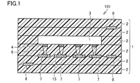
- FIG. 1 A cross-sectional view of the resin multilayer substrate 101 in the present embodiment is shown in FIG.
- the resin multilayer substrate 101 in the present embodiment includes a laminated body 1 in which a plurality of resin layers 2 mainly made of a thermoplastic resin are laminated, a component 3 built in the laminated body 1, and a laminated body 1.
- positioned at a clearance gap and have an outline when it sees from one side of the lamination direction of the laminated body 1 are provided.
- the thermoplastic resin as the main material of the resin layer 2 is, for example, a liquid crystal polymer (LCP).
- the plurality of resin layers 2 may all have the same thickness.
- the plurality of resin layers 2 may be a combination of resin layers having different thicknesses.
- the component 3 includes a plurality of electrodes 4 on the lower surface. Each of the electrodes 4 is electrically connected to a conductor pattern located below via a conductor via 6.
- the shape and structure of the component 3 shown here are merely examples.
- the component may include an electrode in addition to the lower surface. The shape when the part is viewed in a sectional view is not necessarily a rectangle.
- the first-type conductor pattern 7 is arranged at least at one interface inside the resin multilayer substrate 101.
- the positional relationship when this interface is viewed from the upper side in FIG. Shown in “Lamination direction” refers to the vertical direction in FIG. “When viewed from one side in the stacking direction” means, for example, when the stacked body 1 shown in FIG. 1 is viewed from above or below.
- “When viewed from one side in the stacking direction” means, for example, when the stacked body 1 shown in FIG. 1 is viewed from above or below.
- the appearance of “when viewed from one side in the stacking direction” will be described while showing a state viewed from the top to the bottom in FIG. The same applies to the following embodiments.
- the conductor pattern is basically arranged at the interface between the resin layers 2 or arranged on the surface of the resin layer 2 exposed on the surface of the laminate 1, but in the following explanation, the laminate 1
- the plane in which the conductor pattern is located inside or on the surface of the substrate may be referred to as a “layer”.
- the conductor pattern may be formed of a metal foil or a metal film.
- the conductor pattern may be formed of any metal such as copper, aluminum, gold, and silver.
- one or more first type conductor patterns 7 are arranged in one layer, and a second type conductor pattern 8 is also arranged in the same layer.
- at least one second-type conductor pattern 8 may be arranged in layers having different heights in the resin multilayer substrate 101.
- one or more first-type conductor patterns 7 are all arranged at the same height, but this is only an example, and at least one first-type conductor pattern at different heights.
- the conductor pattern 7 may be arranged.
- the component 3 is positioned on the near side of the paper surface, but the outline of the component 3 projected onto this interface is indicated by a two-dot chain line.
- each outline of the first type conductor pattern 7 is in a position overlapping the component 3 when viewed from one side in the stacking direction of the stacked body 1.
- Each outline of the second type conductor pattern 8 is in a position where it does not overlap with the component 3 at all when viewed from one side in the stacking direction of the multilayer body 1.
- thermoplastic resin powder for example, a liquid crystal polymer powder
- the resin part 15 which is derived from the resin paste and in which the liquid component of the resin paste does not substantially remain is disposed.
- the resin portion 15 is not disposed in a portion along each outline of the second type conductor pattern 8. This is because, if the resin part 15 is arranged in a portion along each outer shape line of the second type conductor pattern 8, the resin part 15 is arranged in a place where there is no problem of the above-mentioned unjoined, and the laminate is unnecessarily formed. This is because there is a possibility that a problem that the thickness of the laminate increases and a problem that the coplanarity of the surface of the laminate is deteriorated may occur.
- the heat and pressure transmission in the thermocompression bonding process is somewhat blocked by the part 3, so there is a possibility that the acting heat and pressure may be insufficient.
- an unbonded portion is generated in the vicinity of the outline
- the resin portion 15 since the resin portion 15 is disposed in such a portion, the resin portion fills the gap in the vicinity of the outline of the conductor pattern. It will be. Therefore, it is possible to eliminate the unbonded state between the resin layers in a place where the action of the heat and pressure of the press in the thermocompression bonding process tends to be insufficient.
- the resin paste which comprises the resin part 15 will be in the state which the liquid component of the resin paste vaporizes and does not remain substantially with the heat and pressure in said thermocompression bonding process.
- At least one first-type conductor pattern 7 is arranged at a position where the outline of the first-type conductor pattern 7 overlaps the outline of the component 3.
- the relationship is just an example.
- at least one first-type conductor pattern 7 may be positioned so as to straddle the outline of the component 3.
- the resin portion 15 may be disposed along only the portion of the outline of the first type conductor pattern 7 that overlaps the component 3.
- the resin part 15 does not need to be arranged in the part of the outline of the first type conductor pattern 7 that does not overlap the part 3.
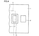
- the configuration is not limited to this. For example, as shown in FIG.
- At least one first-type conductor pattern 7 is positioned so as to straddle the outline of the component 3, and in the outline of the first-type conductor pattern 7, the component 3
- the resin portion 15 may be arranged so as to extend not only to the overlapping portion but also to the non-overlapping portion. 3 and 4, the resin portion 15 is not disposed along the outline of the second type conductor pattern 8 that does not have any part overlapping the component 3.
- the resin portion 15 is formed by applying a resin paste to a desired region and vaporizing a liquid component in the resin paste. Therefore, the resin portion 15 is in a state where the liquid component in the resin paste is not substantially left, in other words, only the resin component in the resin paste is substantially left.
- the resin paste used when forming the resin portion 15 may be a powdery thermoplastic resin, for example, a powdery liquid crystal polymer dispersed in a liquid.
- a liquid component for dispersing the powdered thermoplastic resin that is, a dispersion medium, for example, ethanol, terpineol, butyl lactone, isopropyl alcohol, or the like can be used.
- a liquid component preferably does not contain a binder.
- the surface treatment is performed by plasma or ultraviolet rays.
- the powdery liquid crystal polymer is improved in bonding properties by being subjected to surface treatment with plasma or ultraviolet rays.
- the bondability between the liquid crystal polymer particles is improved, and the strength of the resin portion 15 itself is increased.
- the bondability between the liquid crystal polymer particles and the surface of the resin layer 2 is improved, the bonding strength between the resin portion 15 and the resin layer 2 is also increased.
- the effect is particularly great when the resin layer 2 is made of a liquid crystal polymer. As a result, a resin multilayer substrate having increased strength as a whole can be obtained.
- the surface treatment with ultraviolet rays is more preferable than the surface treatment with plasma because the effect of improving the bondability is greater.
- the resin paste as the material of the resin portion 15 preferably contains a varnish-like liquid crystal polymer.
- the varnish-like liquid crystal polymer can be obtained by dissolving a solvent-soluble liquid crystal polymer in a solvent.
- a varnish-like liquid crystal polymer is different from a powder-like liquid crystal polymer dispersed in a liquid, and individual particles are completely dissolved in a solvent.
- n-methylpyrrolidone when used as a solvent, a solvent-insoluble liquid crystal polymer is used as the resin layer 2, while a resin paste as a material for the resin portion 15 has a part of the molecular structure. It is preferable to use a liquid crystal polymer that contains an amide bond or the like and is soluble in this solvent.
- the resin paste used for forming the resin portion 15 includes a fibrillated liquid crystal polymer powder.
- the liquid crystal polymer powder thus fibrillated is included so that the paste can easily pass through, for example, a screen-printed mesh.
- the viscosity of the resin paste can be easily increased by including the liquid crystal polymer powder thus fibrillated.
- the fibrillated liquid crystal polymer powder has a large change in thickness due to compression compared to, for example, spherical or granular liquid crystal polymer powder, even when thickly applied, the thermocompression bonding process is completed.
- the resin portion 15 can easily have the same thickness as the conductor pattern or almost the same thickness.
- FIG. 5 shows a cross-sectional view of the resin multilayer substrate 102 in the present embodiment.
- the resin portion 15 is only formed with a constant width along the portion of the outline of the first type conductor pattern 7 that overlaps the component 3.
- the resin portion 15 is covered so as to cover the entire region not covered with the first type conductor pattern 7 in the region overlapping the component 3. Is arranged.
- the arrangement of the resin portion 15 may be as described above.
- FIG. 6 shows the positional relationship when the layer of the first type conductor pattern 7 in the resin multilayer substrate 102 is viewed from the upper side in FIG.
- the outline of the resin portion 15 is displayed slightly shifted from the outline of the component 3, but the two may match.
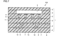
- FIG. 7 shows a cross-sectional view of the resin multilayer substrate 103 in the present embodiment.
- the conductor pattern closest to the component 3 below the component 3 is the first type conductor pattern 7, but in the present embodiment, the first type conductor pattern is provided.
- Another conductor pattern 11 is located between 7 and the part 3.
- the electrode 4 provided on the lower surface of the component 3 and the conductor pattern 11 are electrically connected by the conductor via 6.
- the conductor pattern 11 and the first type conductor pattern 7 may be electrically connected or may not be connected. In this way, a configuration in which the conductor pattern located closest to the component 3 is not the first type conductor pattern 7 may be used. In other words, a configuration in which a conductor pattern other than the first type conductor pattern 7 is located between the first type conductor pattern 7 and the component 3 may be employed.
- the first type conductor pattern 7 is electrically connected to the other conductor pattern 12 further below by the conductor via 6. This is merely an example and is not limited to such a configuration.
- All of the conductor patterns arranged in the laminate 1 are not necessarily classified as either the first type conductor pattern or the second type conductor pattern. There may be a conductor pattern that is neither the first type conductor pattern nor the second type conductor pattern while being inside the multilayer body 1 like the above-described conductor pattern 11.
- not all of the conductor pattern in which at least a part of the outline overlaps with the part is necessarily the first type conductor pattern.
- Embodiment 4 With reference to FIG. 8, the resin multilayer substrate in Embodiment 4 based on this invention is demonstrated.
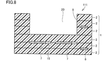
- a cross-sectional view of the resin multilayer substrate 111 in the present embodiment is shown in FIG.
- the resin multilayer substrate 111 has a cavity 20.
- a cavity is a recess.
- a cavity 20 is formed when a part of the laminate 1 is recessed.
- the number of layers of the resin layer 2 may be different between the portion of the cavity 20 and the portion other than the cavity 20.
- the cavity 20 can be grasped as a low part surrounded by a high part.
- the cavity 20 may be completely surrounded by a high part when viewed from one side in the stacking direction, but may have a structure in which only a part of the outer periphery is in contact with a high part. That is, in the present invention, the “cavity” refers to a concave portion having a structure in which a part of the outer periphery is in contact with a high portion. Note that when viewed from one side in the stacking direction, a part of the side of the cavity may be connected to the end of the stack.
- the resin multilayer substrate 111 includes a laminated body 1 in which a plurality of resin layers 2 mainly composed of a thermoplastic resin are laminated, a cavity 20 provided so as to dig into the laminated body 1 in the laminating direction, and the laminated body 1.
- the one or more first-type conductor patterns 7 that are disposed in the gaps between the resin layers 2 and have an outline when viewed from one side in the stacking direction of the multilayer body 1, and the resin layers 2 within the multilayer body 1
- one or more second-type conductor patterns 8 having an outline when viewed from one side in the stacking direction of the multilayer body 1.
- each outline of the first type conductor pattern 7 is in a position overlapping the cavity 20 when viewed from one side in the stacking direction of the multilayer body 1.
- Each outline of the second type conductor pattern 8 is in a position where it does not overlap the cavity 20 when viewed from one side in the stacking direction of the multilayer body 1.
- a thermoplastic resin powder for example, a liquid crystal polymer powder, is used as a main material so as to be adjacent to the outside of the first type conductor pattern 7 along the portion of each outline line of the first type conductor pattern 7 that overlaps the cavity 20.
- the resin part 15 which is derived from the resin paste and in which the liquid component of the resin paste does not substantially remain is disposed.
- the resin portion 15 is not disposed in a portion along each outline of the second type conductor pattern 8.
- one or more second type conductor patterns 8 are all located in different layers from the first type conductor pattern 7, but this is only an example, and at least one type The second type conductor pattern 8 may be located in the same layer as the first type conductor pattern 7.
- the heat and pressure of the press may not reach the bottom of the cavity in some cases, and the action of heat and pressure may be insufficient in the thermocompression bonding process.
- the resin portion 15 is disposed in such a portion, the resin portion is a gap near the outline of the conductor pattern. Will be filled. Therefore, it is possible to eliminate the unbonded state between the resin layers in a place where the action of the heat and pressure of the press in the thermocompression bonding process tends to be insufficient.
- FIG. 9 shows a resin multilayer substrate 112.
- the resin multilayer substrate 112 includes the first type conductor pattern 7 in two layers.
- One or more first-type conductor patterns 7 are arranged in each layer.
- the plurality of first type conductor patterns 7 may be arranged in a plurality of layers. This is true not only in the fourth embodiment but also in other embodiments.
- the resin multilayer substrate 121 includes a first conductor foil 25.
- the first conductor foil 25 has the maximum thickness among the conductor foils included in the resin multilayer substrate 121.
- the concept of conductor foil here includes a conductor pattern.
- the first conductor foil 25 is also referred to as “maximum thickness conductor foil”.
- the first conductor foil 25 may be a kind of copper foil. When the first conductor foil 25 is made of copper, the first conductor foil 25 is also referred to as “maximum thickness copper foil”.
- the resin multilayer substrate 121 includes a laminated body 1 in which a plurality of resin layers 2 mainly composed of a thermoplastic resin are laminated, a first conductor foil 25 incorporated in the laminated body 1, and an inside of the laminated body 1.
- 1 or more 1st type conductor patterns 7 which are arrange
- one or more second-type conductor patterns 8 that are arranged and have an outline when viewed from one side in the stacking direction of the multilayer body 1.
- the first conductive foil 25 is thicker than any of the one or more first type conductor patterns 7 and the one or more second type conductor patterns 8. At least a part of each outline of the first type conductor pattern 7 is in a position overlapping the first conductor foil 25 when viewed from one side in the stacking direction of the multilayer body 1. Each outline of the second type conductor pattern 8 is in a position where it does not overlap with the first conductor foil 25 when viewed from one side in the stacking direction of the multilayer body 1.
- a powder of a thermoplastic resin for example, a liquid crystal polymer powder, so as to be adjacent to the outside of the first type conductor pattern 7 along a portion of each outer shape line of the first type conductor pattern 7 that overlaps the first conductor foil 25.
- a resin portion 15 is disposed which is derived from a resin paste whose main material is and in which the liquid component of the resin paste does not substantially remain. The resin portion 15 is not disposed in a portion along each outline of the second type conductor pattern 8.
- FIG. 11 shows a resin multilayer substrate 122.
- the resin multilayer substrate 122 includes the first type conductor pattern 7 in two layers.
- the plurality of first type conductor patterns 7 may be arranged in a plurality of layers.
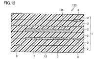
- FIG. 12 shows a resin multilayer substrate 123.
- the region other than the first type conductor pattern 7 is entirely covered with the resin portion 15 in the portion overlapping the first conductor foil 25.
- Such a configuration may be used.
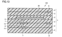
- FIG. 13 shows a resin multilayer substrate 124.
- the first conductor foil 25 and at least one of the first type conductor pattern 7 are electrically connected through the conductor via 6.
- the plurality of first-type conductor patterns 7 are arranged in different layers.
- the first-type conductor patterns 7 in different layers are electrically connected through the conductor vias 6.
- the first type conductor pattern 7 is arranged only on the first conductor foil 25 and the lower side of the first conductor foil 25, but the first type conductor pattern 7 is arranged. May be above the first conductor foil 25.
- the first type conductor pattern 7 may be arranged on both the upper side and the lower side of the first conductor foil 25.
- the first conductor foil 25 and the first type conductor pattern 7 on the lower side of the first conductor foil 25 are connected by the conductor via 6, and the first conductor foil 25 and the first conductor foil 25 are connected to each other.
- the first via pattern 7 on the upper side of the conductor foil 25 may be connected by the conductor via 6.
- a resin sheet with a conductive foil is prepared.
- the conductor foil may be a metal foil, for example.
- the conductor foil may be a copper foil, for example.
- a resist pattern is printed on the surface of the conductor foil of the resin sheet with conductor foil.
- a resist pattern here is a pattern by the resist layer which has the shape corresponding to a desired conductor pattern. Using the resist pattern as a mask, the portion of the conductive foil not covered with the resist is removed with an acid.
- the acid can be, for example, HCl.
- the resist pattern is removed with an alkaline solution. Neutralize if necessary. In this way, a part of the conductor foil remains in a desired shape, that is, a conductor pattern is obtained on the surface of the resin sheet.
- a plurality of conductor patterns are formed.
- the plurality of conductor patterns include a first type conductor pattern 7 and a second type conductor pattern 8.
- the resin sheet becomes the resin layer 2.
- FIG. 14 shows a state in which the first type conductor pattern 7 is arranged on the surface of the resin layer 2.
- ⁇ Laser processing is performed from the surface of the resin layer 2 where the conductor pattern is not present. Through holes are formed in the resin sheet by this laser processing. This through hole is filled with a conductive paste. Thus, a conductor via is obtained at a desired location on the resin sheet.
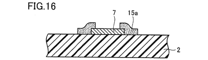
- FIG. 15 shows a case where the first type conductor pattern 7 is arranged on the surface of the resin layer 2 and the resin paste 15 a is arranged along the outline of the first type conductor pattern 7.
- the end of the first type conductor pattern 7 may be partially covered with the resin paste 15a.
- thermocompression bonding process is performed on the stack.
- the resin paste disposed along part or all of the outline of the conductor pattern is deformed by heat and pressure, and as shown in FIG. 18, the gap between the resin layers or the conductor pattern and the resin layer
- the resin portion 15 is formed so as to fill the gap.
- the resin part 15 is in a state in which no liquid component substantially remains.
- the laminated body 1 is integrated and a resin multilayer substrate is obtained. Even if the resin paste partially covers the end portion of the first type conductor pattern 7 due to this deformation, the resin paste flows and flows outside the outline of the first type conductor pattern 7. Moreover, each resin sheet becomes the resin layer 2.
- the conductor paste that has formed the conductor vias is solidified and completed as a conductor via.
- the first type conductor pattern 7 is formed on the surface of the resin layer 2, and the resin paste 15a is disposed so as to surround the first type conductor pattern 7.
- the method is not limited thereto. Instead, the method shown in FIG. 19 may be used. That is, the first type conductor pattern 7 is formed on the surface of the resin layer 2, and the resin paste 15a is not formed on the surface of the resin layer 2 on which the first type conductor pattern 7 is formed, but on the surface of the other resin layer 2. Has been placed.
- the resin paste 15 a is arranged in a shape corresponding to the outline of the first type conductor pattern 7. As shown in FIG.
- the first resin layer 2 on which the first-type conductor pattern 7 is arranged and the second resin layer 2 on which the resin paste 15a is arranged are overlapped and thermocompression bonded.
- a state as shown in FIG. 18 can be obtained. Such a method may be adopted.
- the resin multilayer substrate in Embodiment 6 With reference to FIG. 20, the resin multilayer substrate in Embodiment 6 based on this invention is demonstrated.
- a cross-sectional view of the resin multilayer substrate 131 in the present embodiment is shown in FIG.
- the resin multilayer substrate 131 includes the component 3.
- the resin multilayer substrate 131 includes a conductor via first type joint portion 17 and a conductor via second type joint portion 18.
- the resin multilayer substrate 131 includes a laminate 1 in which a plurality of resin layers 2 mainly composed of a thermoplastic resin are laminated, a component 3 built in the laminate 1, and a plurality of resins in the laminate 1. It is a portion where conductor vias arranged so as to penetrate any one of the layers 2 are joined together so as to be continuous in the stacking direction of the multilayer body 1, and are joined when viewed from one side in the stacking direction of the multilayer body 1.
- the laminated body 1 is composed of one or more conductive via first-type joints 17 having a surface outline, and conductive vias arranged so as to penetrate through any of the plurality of resin layers 2 inside the laminated body 1.
- the conductor via 2nd type junction part 18 which has the outline of a joining surface.
- the conductor via 6a has a tapered shape whose diameter increases toward the upper side in FIG.
- the conductor via 6b has a tapered shape whose diameter increases toward the lower side in FIG.
- the end face having the larger diameter of the conductor via 6a and the end face having the larger diameter of the conductor via 6b face each other and are joined. The same applies to the conductor via type 2 junction 18.
- each outline of the conductor via first type joint portion 17 is in a position overlapping the part 3 when viewed from one side in the stacking direction of the stacked body 1.
- Each outline of the conductor via type 2 junction 18 is in a position where it does not overlap the component 3 at all when viewed from one side in the stacking direction of the stacked body 1.
- a powder of a thermoplastic resin for example, a liquid crystal polymer, is formed so as to be adjacent to the outside of the conductor via first type joint portion 17 along a portion overlapping each component 3 in each outer shape line of the conductor via first type joint portion 17.
- a resin portion 15 is disposed which is derived from a resin paste whose main material is powder and in which the liquid component of the resin paste does not substantially remain. The resin portion 15 is not disposed in a portion along each outer shape line of the conductor via second type joint portion 18.
- the heat and pressure transmission in the thermocompression bonding process is somewhat blocked by the part 3, so there is a possibility that the acting heat and pressure may be insufficient, and as a result, the conductor via first-type bonding
- a part where the resin layer is in an unjoined state may occur in the vicinity of the part.
- the resin part 15 is disposed in such a part, the resin part is a joint part between the conductor vias. The gap in the vicinity of the outer shape line will be filled. Therefore, it is possible to eliminate the unbonded state between the resin layers in a place where the action of the heat and pressure of the press in the thermocompression bonding process tends to be insufficient.
- FIG. 21 A cross-sectional view of resin multilayer substrate 132 in the present embodiment is shown in FIG.
- the resin multilayer substrate 132 includes the cavity 20.
- the resin multilayer substrate 132 includes a conductor via first type joint portion 17 and a conductor via second type joint portion 18.
- the resin multilayer substrate 132 includes a laminate 1 in which a plurality of resin layers 2 mainly composed of a thermoplastic resin are laminated, a cavity 20 provided so as to dig into the laminate 1 in the laminating direction, and the laminate 1. Is a portion where conductor vias arranged so as to penetrate through any of the plurality of resin layers 2 are joined along the stacking direction of the multilayer body 1, and in the stacking direction of the multilayer body 1.
- one or more conductor via first-type joints 17 having a joint surface outline, and conductor vias arranged so as to penetrate through any of the plurality of resin layers 2 inside the laminate 1 Is a portion joined so as to be continuous along the stacking direction of the multilayer body 1, and when viewed from one side in the stacking direction of the multilayer body 1, one or more conductor via second-type joint portions having a joint line outline 18.
- At least a part of each outline of each of the conductor via first type joints 17 is located at a position overlapping with the cavity 20 when viewed from one side in the stacking direction of the multilayer body 1.
- the outline is in a position that does not overlap the cavity 20 when viewed from one side in the stacking direction of the stacked body 1.
- a powder of a thermoplastic resin for example, a liquid crystal polymer, is disposed so as to be adjacent to the outside of the conductor via first type joint portion 17 along the portion overlapping each of the outer shapes of the conductor via first type joint portion 17 with the cavity 20.
- a resin portion 15 is disposed which is derived from a resin paste whose main material is powder and in which the liquid component of the resin paste does not substantially remain. The resin portion 15 is not disposed in a portion along each outer shape line of the conductor via second type joint portion 18.
- the resin portion 15 is arranged in such a portion, the resin portion fills a gap in the vicinity of the outline of the joint portion between the conductor vias. Therefore, it is possible to eliminate the unbonded state between the resin layers in a place where the action of the heat and pressure of the press in the thermocompression bonding process tends to be insufficient.
- the resin multilayer substrate 141 includes a first conductor foil 25.
- the resin multilayer substrate 141 includes a conductor via first type joint portion 17 and a conductor via second type joint portion 18.
- the resin multilayer substrate 141 includes a laminated body 1 in which a plurality of resin layers 2 mainly composed of a thermoplastic resin are laminated, a first conductor foil 25 incorporated in the laminated body 1, and the inside of the laminated body 1.
- a portion where conductor vias arranged so as to penetrate through any one of the plurality of resin layers 2 are joined together so as to be continuous in the stacking direction of the multilayer body 1, as viewed from one side in the stacking direction of the multilayer body 1.
- 1 or more conductor via first type joint part 17 which has the outline of a joint surface, and conductor vias arranged so that one of a plurality of resin layers 2 may be penetrated inside laminate 1 is a laminate.
- 1 is a portion that is joined so as to be continuous along the laminating direction, and includes at least one conductor via second type joint portion having an outline of a joining surface when viewed from one side in the laminating direction of the laminate 1. .
- the first conductor foil 25 is thicker than any conductor foil existing inside the multilayer body 1. At least a part of each outer shape line of the conductor via first type joint portion 17 is in a position overlapping the first conductor foil 25 when viewed from one side in the stacking direction of the multilayer body 1. Each outline of the conductor via type 2 junction 18 is in a position where it does not overlap the first conductor foil 25 when viewed from one side in the stacking direction of the multilayer body 1.
- a powder of a thermoplastic resin for example, so as to be adjacent to the outside of the conductor via first type joint portion 17 along a portion overlapping each of the first conductor foils 25 in each outer shape line of the conductor via first type joint portion 17, for example,
- a resin portion 15 is disposed which is derived from a resin paste mainly composed of liquid crystal polymer powder, and in which the liquid component of the resin paste does not substantially remain.
- the resin portion 15 is not disposed in a portion along each outer shape line of the conductor via second type joint portion 18.
- the thickness of the first type conductor foil 25 is thick and the rigidity of this portion is relatively high, so that deformation along the shape of the laminate is less likely to occur in the thermocompression bonding step. .
- heat and pressure acting in the thermocompression bonding process may be insufficient, and as a result, there is a possibility that an unjoined part may occur in the vicinity of the conductor via first type joint part.
- the resin portion 15 since the resin portion 15 is disposed in such a portion, the resin portion fills a gap in the vicinity of the outline of the joint portion between the conductor vias. Therefore, it is possible to eliminate the unbonded state between the resin layers in a place where the action of the heat and pressure of the press in the thermocompression bonding process tends to be insufficient.
- FIG. 23 shows a resin multilayer substrate 142.
- the resin portion 15 is arranged so as to connect a plurality of conductor via first type joint portions 17 arranged in the same layer. Such a configuration may be used.
- thermoplastic resin that is the main material of the resin layer 2 is a liquid crystal polymer
- thermoplastic resin of the resin portion 15 is a liquid crystal polymer.
- the liquid crystal polymer that is the main material of the resin layer 2 and the liquid crystal polymer of the resin portion 15 are preferably made of substantially the same type of liquid crystal polymer material.
Landscapes
- Engineering & Computer Science (AREA)
- Microelectronics & Electronic Packaging (AREA)
- Manufacturing & Machinery (AREA)
- Production Of Multi-Layered Print Wiring Board (AREA)
- Structure Of Printed Boards (AREA)
Abstract
樹脂多層基板(101)は、複数の樹脂層(2)を積層したものである積層体(1)と、部品(3)と、1以上の第1種導体パターン(7)と、積層体(1)の内部で樹脂層(2)同士の隙間に配置され、1以上の第2種導体パターン(8)とを備え、第1種導体パターン(7)の各々の外形線の少なくとも一部は、部品(3)と重なる位置にあり、第2種導体パターン(8)の各々の外形線は、部品(3)と全く重ならない位置にあり、第1種導体パターン(7)の各々の外形線のうち部品(3)と重なる部分に沿って、第1種導体パターン(7)の外側に隣接するように、熱可塑性樹脂の粉末を主材料とする樹脂ペースト由来の樹脂部(15)が配置されており、第2種導体パターン(8)の各々の外形線に沿う部分には樹脂部(15)が配置されていない。
Description
本発明は、樹脂多層基板に関するものである。
複数の樹脂層を積み重ねて積層体とし、これを熱圧着することによって樹脂多層基板を作製する例が、特開2014-225604号公報(特許文献1)に記載されている。
特許文献1に記載されているように、積層体にキャビティを設けておき、このキャビティ内に部品を配置し、この状態で熱圧着を行なうことによって、部品を内蔵した樹脂多層基板を作製することも可能である。
たとえば、樹脂多層基板が部品を内蔵する積層体であって、かつ、内蔵される部品の真下に導体パターンがある場合に、この導体パターンに隣接する部分では、熱圧着工程を終えた後においても樹脂層同士の接合が不十分となる場合があった。このような部分が部品の真下に隠れることによって、熱圧着工程におけるプレスの熱や圧力が部品の真下に隠れていない箇所と比較して十分に伝わらないことが原因と考えられる。
部品の真下以外にも、積層体に積層方向に掘り下げるように設けられたキャビティを設ける場合におけるキャビティの真下においても同様の問題が生じうる。他にもいくつかの場合に同様の問題が生じうる。
そこで、本発明は、熱圧着工程におけるプレスの熱や圧力の作用が不十分となりがちな箇所における樹脂層間の未接合状態を解消した樹脂多層基板を提供することを目的とする。
上記目的を達成するため、本発明に基づく樹脂多層基板は、熱可塑性樹脂を主材料とする複数の樹脂層を積層したものである積層体と、上記積層体に内蔵された部品と、上記積層体の内部で上記樹脂層同士の隙間に配置され、上記積層体の積層方向の一方から見たとき外形線を有する1以上の第1種導体パターンと、上記積層体の内部で上記樹脂層同士の隙間に配置され、上記積層体の積層方向の一方から見たとき外形線を有する1以上の第2種導体パターンとを備える。上記第1種導体パターンの各々の外形線の少なくとも一部は、上記積層体の積層方向の一方から見たとき上記部品と重なる位置にある。上記第2種導体パターンの各々の外形線は、上記積層体の積層方向の一方から見たとき上記部品と全く重ならない位置にある。上記第1種導体パターンの各々の外形線のうち上記部品と重なる部分に沿って、上記第1種導体パターンの外側に隣接するように、熱可塑性樹脂の粉末を主材料とする樹脂ペースト由来であり、この樹脂ペーストの液体成分が実質的に残留していない樹脂部が配置されている。上記第2種導体パターンの各々の外形線に沿う部分には上記樹脂部が配置されていない。
本発明によれば、樹脂部が配置されているので、熱圧着工程におけるプレスの圧力の作用が不十分となりがちな箇所における樹脂層間の未接合状態を解消した樹脂多層基板とすることができる。
図面において示す寸法比は、必ずしも忠実に現実のとおりを表しているとは限らず、説明の便宜のために寸法比を誇張して示している場合がある。以下の説明において、上または下の概念に言及する際には、絶対的な上または下を意味するとは限らず、図示された姿勢の中での相対的な上または下を意味する場合がある。
(実施の形態1)
図1~図2を参照して、本発明に基づく実施の形態1における樹脂多層基板について説明する。本実施の形態における樹脂多層基板101の断面図を図1に示す。
図1~図2を参照して、本発明に基づく実施の形態1における樹脂多層基板について説明する。本実施の形態における樹脂多層基板101の断面図を図1に示す。
本実施の形態における樹脂多層基板101は、熱可塑性樹脂を主材料とする複数の樹脂層2を積層したものである積層体1と、積層体1に内蔵された部品3と、積層体1の内部で樹脂層2同士の隙間に配置され、積層体1の積層方向の一方から見たとき外形線を有する1以上の第1種導体パターン7と、積層体1の内部で樹脂層2同士の隙間に配置され、積層体1の積層方向の一方から見たとき外形線を有する1以上の第2種導体パターンとを備える。樹脂層2の主材料としての熱可塑性樹脂は、たとえば液晶ポリマー(LCP)である。複数の樹脂層2は、いずれも同じ厚みであってもよい。複数の樹脂層2は、異なる厚みの樹脂層同士を組み合わせたものであってもよい。
部品3は、下面に複数の電極4を備えている。電極4の各々は、下方に位置する導体パターンに対して導体ビア6を介して電気的に接続されている。ここで示す部品3の形状、構造は、あくまで一例である。部品は下面以外に電極を備えていてもよい。部品を断面図で見たときの形状は、長方形とは限らない。
図1に示した例では、樹脂多層基板101の内部の少なくとも1つの界面に第1種導体パターン7が配置されているが、この界面を図1における上側から見たときの位置関係を図2に示す。「積層方向」とは、図1における上下方向のことである。「積層方向の一方から見たとき」というのは、たとえば図1に示した積層体1を上または下から見たときという意味である。ここでは説明の便宜のために、「積層方向の一方から見たとき」の見え方に関しては、図1における上から下に向かって見た状態を示しながら説明する。以下の実施の形態においても同様である。
導体パターンは、基本的に樹脂層2同士の界面に配置されるか、積層体1の表面に露出する樹脂層2の表面に配置されるものであるが、以下の説明中では、積層体1の内部または表面で導体パターンが位置する平面のことを「層」という場合がある。
導体パターンは、金属箔または金属膜によって形成されたものであってよい。導体パターンは、たとえば銅、アルミニウム、金、銀などのいずれかの金属で形成されたものであってもよい。
図2に示すように、ある1つの層に1以上の第1種導体パターン7が配置されており、同じ層に第2種導体パターン8も配置されている。図1、図2に示すように、樹脂多層基板101の中で異なる高さの層にも少なくとも1つの第2種導体パターン8が配置されていてもよい。図1、図2に示した例では、1以上の第1種導体パターン7は全て同じ高さに配置されているが、これはあくまで一例であって、異なる高さに少なくとも1つの第1種導体パターン7が配置されていてもよい。図2においては、部品3は紙面より手前側に位置するが、部品3をこの界面に投影した輪郭が二点鎖線で示されている。
図2に示すように、第1種導体パターン7の各々の外形線の少なくとも一部は、積層体1の積層方向の一方から見たとき部品3と重なる位置にある。第2種導体パターン8の各々の外形線は、積層体1の積層方向の一方から見たとき部品3と全く重ならない位置にある。
第1種導体パターン7の各々の外形線のうち部品3と重なる部分に沿って、第1種導体パターン7の外側に隣接するように、熱可塑性樹脂の粉末、たとえば液晶ポリマーの粉末を主材料とする樹脂ペースト由来であり、この樹脂ペーストの液体成分が実質的に残留していない樹脂部15が配置されている。第2種導体パターン8の各々の外形線に沿う部分には樹脂部15が配置されていない。これは、第2種導体パターン8の各々の外形線に沿う部分に樹脂部15を配置すると、上述の未接合の問題がない箇所に樹脂部15が配置されることとなり、不必要に積層体の厚みが増すという問題、また、かえって積層体の表面のコプラナリティが劣化するといった問題が発生するおそれがあるからである。
部品3と重なる部分においては、熱圧着工程における熱や圧力の伝達が部品3によっていくらか遮られるので、作用する熱や圧力が不十分となる可能性があり、その結果、第1種導体パターンの外形線近傍において未接合状態の部分が生じるおそれがあるが、本実施の形態では、そのような部分に樹脂部15が配置されているので、樹脂部が導体パターンの外形線近傍の隙間を埋めることとなる。したがって、熱圧着工程におけるプレスの熱や圧力の作用が不十分となりがちな箇所における樹脂層間の未接合状態を解消することができる。なお、樹脂部15を構成する樹脂ペーストは、上記の熱圧着工程における熱および圧力によって、樹脂ペーストの液体成分が気化して実質的に残留していない状態となる。
(位置関係のバリエーション)
図2に示した例では、少なくとも1つの第1種導体パターン7は、第1種導体パターン7の外形線が部品3の外形線と重なるような位置に配置されているが、このような位置関係はあくまで一例である。たとえば図3に示すように、少なくとも1つの第1種導体パターン7は、部品3の外形線にまたがるように位置していてもよい。このような場合、図3に示すように、樹脂部15は、第1種導体パターン7の外形線のうち部品3と重なる部分のみに沿って配置されていてもよい。第1種導体パターン7の外形線のうち部品3と重ならない部分には、樹脂部15が配置されていなくてよい。しかし、このような構成に限るものではない。たとえば図4に示すように、少なくとも1つの第1種導体パターン7が、部品3の外形線にまたがるように位置していて、かつ、この第1種導体パターン7の外形線においては、部品3と重なる部分だけでなく重ならない部分にまで沿うように樹脂部15が配置されていてもよい。図3、図4に示すような場合にも、部品3と重なる部分を全く有していない第2種導体パターン8の外形線に沿っては樹脂部15が配置されていない。
図2に示した例では、少なくとも1つの第1種導体パターン7は、第1種導体パターン7の外形線が部品3の外形線と重なるような位置に配置されているが、このような位置関係はあくまで一例である。たとえば図3に示すように、少なくとも1つの第1種導体パターン7は、部品3の外形線にまたがるように位置していてもよい。このような場合、図3に示すように、樹脂部15は、第1種導体パターン7の外形線のうち部品3と重なる部分のみに沿って配置されていてもよい。第1種導体パターン7の外形線のうち部品3と重ならない部分には、樹脂部15が配置されていなくてよい。しかし、このような構成に限るものではない。たとえば図4に示すように、少なくとも1つの第1種導体パターン7が、部品3の外形線にまたがるように位置していて、かつ、この第1種導体パターン7の外形線においては、部品3と重なる部分だけでなく重ならない部分にまで沿うように樹脂部15が配置されていてもよい。図3、図4に示すような場合にも、部品3と重なる部分を全く有していない第2種導体パターン8の外形線に沿っては樹脂部15が配置されていない。
(樹脂部)
樹脂部15は、樹脂ペーストを所望領域に塗布し、樹脂ペースト中の液体成分を気化させることによって形成されたものである。したがって、樹脂部15は、樹脂ペースト中の液体成分が実質的に残留していない状態、言い換えれば、樹脂ペースト中の樹脂成分のみが実質的に残留している状態のものとなっている。樹脂部15を形成する際に用いられる樹脂ペーストは、パウダー状の熱可塑性樹脂、たとえばパウダー状の液晶ポリマーを液体に分散させたものであってよい。パウダー状の熱可塑性樹脂を分散させる液体成分、すなわち分散媒としては、たとえばエタノール、ターピネオール、ブチルラクトン、イソプロピルアルコールなどを用いることができる。このような液体成分にはバインダを含まないことが好ましい。
樹脂部15は、樹脂ペーストを所望領域に塗布し、樹脂ペースト中の液体成分を気化させることによって形成されたものである。したがって、樹脂部15は、樹脂ペースト中の液体成分が実質的に残留していない状態、言い換えれば、樹脂ペースト中の樹脂成分のみが実質的に残留している状態のものとなっている。樹脂部15を形成する際に用いられる樹脂ペーストは、パウダー状の熱可塑性樹脂、たとえばパウダー状の液晶ポリマーを液体に分散させたものであってよい。パウダー状の熱可塑性樹脂を分散させる液体成分、すなわち分散媒としては、たとえばエタノール、ターピネオール、ブチルラクトン、イソプロピルアルコールなどを用いることができる。このような液体成分にはバインダを含まないことが好ましい。
ここでいうパウダー状の熱可塑性樹脂としてパウダー状の液晶ポリマーを用いる場合、プラズマまたは紫外線による表面処理がされたものであることが好ましい。パウダー状の液晶ポリマーは、プラズマまたは紫外線による表面処理を施されることによって接合性が向上する。このような表面処理を施されたものを樹脂ペーストの材料に用いることによって、液晶ポリマーの粒子同士の接合性が向上し、樹脂部15自体の強度が増す。また、液晶ポリマーの粒子と樹脂層2表面との間の接合性も向上するので、樹脂部15と樹脂層2との接合強度も増す。特に樹脂層2が液晶ポリマーからなるものである場合にその効果が大きい。その結果、全体として強度が増した樹脂多層基板を得ることができる。なお、パウダー状の液晶ポリマーに対しては、プラズマによる表面処理よりも紫外線による表面処理の方が接合性向上効果が大きいので、より好ましい。
樹脂部15の材料としての樹脂ペーストは、ワニス状の液晶ポリマーを含むことが好ましい。ワニス状の液晶ポリマーは、溶剤可溶型の液晶ポリマーを溶剤に溶解させることによって得ることができる。ワニス状の液晶ポリマーは、パウダー状の液晶ポリマーを液体に分散させたものとは異なり、個々の粒子が溶剤に完全に溶解している。なお、このようにワニス状の液晶ポリマーを用いる場合は、溶剤としては、樹脂層2を溶解しない溶剤を選択することが好ましい。すなわち、たとえば溶剤としてn-メチルピロリドンを用いるとした場合、樹脂層2としては溶剤不溶型の液晶ポリマーを用いることとし、一方、樹脂部15の材料としての樹脂ペーストとしては分子構造の一部にアミド結合などを含み、この溶剤に可溶とした液晶ポリマーを用いることが好ましい。
樹脂部15を形成する際に用いる樹脂ペーストは、フィブリル化された液晶ポリマーのパウダーを含むことが好ましい。樹脂ペーストを作製する際には、このようにフィブリル化された液晶ポリマーのパウダーを含ませることにより、たとえばスクリーン印刷のメッシュをペーストが通過しやすくなる。また、このようにフィブリル化された液晶ポリマーのパウダーを含ませることにより、樹脂ペーストの粘度を容易に高めることができる。また、フィブリル化された液晶ポリマーのパウダーは、たとえば球状、粒状の液晶ポリマー粉体に比べて、圧縮による厚みの変化ぶりが大きいので、厚く塗布したとしても、熱圧着工程を終えた時点での樹脂部15としては導体パターンと同じ厚みまたはほぼ同じ厚みにしやすい。
(実施の形態2)
図5~図6を参照して、本発明に基づく実施の形態2における樹脂多層基板について説明する。本実施の形態における樹脂多層基板102の断面図を図5に示す。
図5~図6を参照して、本発明に基づく実施の形態2における樹脂多層基板について説明する。本実施の形態における樹脂多層基板102の断面図を図5に示す。
実施の形態1における樹脂多層基板101(図1を参照)では、樹脂部15は第1種導体パターン7の外形線のうち部品3と重なる部分に沿って一定幅で形成されていたのみであったが、図5に示すように、本実施の形態における樹脂多層基板102においては、部品3と重なる領域内では、第1種導体パターン7が覆っていない領域の全てを覆うように樹脂部15が配置されている。樹脂部15の配置の仕方は、このようなものであってもよい。
樹脂多層基板102のうちの第1種導体パターン7が配置されている層を、図5における上側から見たときの位置関係を図6に示す。図6では、説明の便宜のため、樹脂部15の外形線を部品3の外形線からわずかにずらして表示しているが、両者は一致していてもよい。
本実施の形態においても、実施の形態1と同様の効果を得ることができる。
(実施の形態3)
図7を参照して、本発明に基づく実施の形態3における樹脂多層基板について説明する。本実施の形態における樹脂多層基板103の断面図を図7に示す。
(実施の形態3)
図7を参照して、本発明に基づく実施の形態3における樹脂多層基板について説明する。本実施の形態における樹脂多層基板103の断面図を図7に示す。
実施の形態1における樹脂多層基板101においては、部品3の下方で最も部品3に近いところにある導体パターンが第1種導体パターン7であったが、本実施の形態では、第1種導体パターン7と部品3との間に他の導体パターン11が位置する。部品3の下面に設けられた電極4と導体パターン11とが導体ビア6によって電気的に接続されている。導体パターン11と第1種導体パターン7とは電気的に接続されていてもよく、接続されていなくてもよい。このように、部品3から見て最も近い位置にある導体パターンが第1種導体パターン7ではない構成であってもよい。言い換えれば、第1種導体パターン7と部品3との間に第1種導体パターン7以外の導体パターンが位置する構成であってもよい。図7に示した樹脂多層基板103においては、第1種導体パターン7はさらに下方にある他の導体パターン12に対して、導体ビア6によって電気的に接続されている。これはあくまで一例として示すものに過ぎず、このような構成に限らない。
積層体1の内部に配置されている導体パターンの全てが、第1種導体パターンと第2種導体パターンのいずれかに分類されるとは限らない。上述の導体パターン11のように、積層体1の内部にありながら第1種導体パターンでも第2種導体パターンでもない導体パターンもありうる。
上方から見たときに外形線の少なくとも一部が部品と重なる導体パターンの全てが第1種導体パターンであるとは限らない。上述の導体パターン11のように、外形線の少なくとも一部が部品と重なる導体パターンでありながら第1種導体パターンに該当しない導体パターンもありうる。
本実施の形態においても、実施の形態1と同様の効果を得ることができる。
(実施の形態4)
図8を参照して、本発明に基づく実施の形態4における樹脂多層基板について説明する。本実施の形態における樹脂多層基板111の断面図を図8に示す。樹脂多層基板111は、キャビティ20を有する。キャビティとは凹部である。積層体1の一部が凹むことによってキャビティ20となっている。キャビティ20の部分とキャビティ20以外の部分とでは、樹脂層2の積層数が異なっていてもよい。本実施の形態においては、キャビティ20は、高い部分に囲まれた低い部分として把握することもできる。キャビティ20は積層方向の一方から見たとき外周を完全に高い部分に囲まれていてもよいが、外周のうち一部のみが高い部分に接している構造であってもよい。すなわち、本発明において「キャビティ」とは、凹部であって、外周のうちの一部が高い部分に接している構造のものを指す。なお、積層方向の一方から見たときキャビティの一部の辺は積層体の端部につながっていてもよい。
(実施の形態4)
図8を参照して、本発明に基づく実施の形態4における樹脂多層基板について説明する。本実施の形態における樹脂多層基板111の断面図を図8に示す。樹脂多層基板111は、キャビティ20を有する。キャビティとは凹部である。積層体1の一部が凹むことによってキャビティ20となっている。キャビティ20の部分とキャビティ20以外の部分とでは、樹脂層2の積層数が異なっていてもよい。本実施の形態においては、キャビティ20は、高い部分に囲まれた低い部分として把握することもできる。キャビティ20は積層方向の一方から見たとき外周を完全に高い部分に囲まれていてもよいが、外周のうち一部のみが高い部分に接している構造であってもよい。すなわち、本発明において「キャビティ」とは、凹部であって、外周のうちの一部が高い部分に接している構造のものを指す。なお、積層方向の一方から見たときキャビティの一部の辺は積層体の端部につながっていてもよい。
樹脂多層基板111は、熱可塑性樹脂を主材料とする複数の樹脂層2を積層したものである積層体1と、積層体1に積層方向に掘り下げるように設けられたキャビティ20と、積層体1の内部で樹脂層2同士の隙間に配置され、積層体1の積層方向の一方から見たとき外形線を有する1以上の第1種導体パターン7と、積層体1の内部で樹脂層2同士の隙間に配置され、積層体1の積層方向の一方から見たとき外形線を有する1以上の第2種導体パターン8とを備える。第1種導体パターン7の各々の外形線の少なくとも一部は、積層体1の積層方向の一方から見たときキャビティ20と重なる位置にある。第2種導体パターン8の各々の外形線は、積層体1の積層方向の一方から見たときキャビティ20と全く重ならない位置にある。第1種導体パターン7の各々の外形線のうちキャビティ20と重なる部分に沿って、第1種導体パターン7の外側に隣接するように、熱可塑性樹脂の粉末、たとえば液晶ポリマーの粉末を主材料とする樹脂ペースト由来であり、前記樹脂ペーストの液体成分が実質的に残留していない樹脂部15が配置されている。第2種導体パターン8の各々の外形線に沿う部分には樹脂部15が配置されていない。
図8に示した樹脂多層基板111では、1以上の第2種導体パターン8はいずれも第1種導体パターン7と異なる層に位置しているが、これはあくまで一例であって、少なくとも1つの第2種導体パターン8が第1種導体パターン7と同じ層に位置していてもよい。
キャビティ20と重なる部分においては、プレスの熱や圧力がキャビティの底まで行き渡りにくい場合があり、熱圧着工程において熱や圧力の作用が不十分となる可能性があり、その結果、第1種導体パターンの外形線近傍において未接合状態の部分が生じるおそれがあるが、本実施の形態では、そのような部分に樹脂部15が配置されているので、樹脂部が導体パターンの外形線近傍の隙間を埋めることとなる。したがって、熱圧着工程におけるプレスの熱や圧力の作用が不十分となりがちな箇所における樹脂層間の未接合状態を解消することができる。
(変形例)
本実施の形態における樹脂多層基板の変形例として、図9に示すようなものも考えられる。図9には樹脂多層基板112が示される。樹脂多層基板112は、2つの層に第1種導体パターン7を備える。各層に1以上の第1種導体パターン7が配置されている。このように、複数の第1種導体パターン7は複数の層に分かれて配置されていてもよい。このことは、実施の形態4に限らず他の実施の形態においてもいえることである。
本実施の形態における樹脂多層基板の変形例として、図9に示すようなものも考えられる。図9には樹脂多層基板112が示される。樹脂多層基板112は、2つの層に第1種導体パターン7を備える。各層に1以上の第1種導体パターン7が配置されている。このように、複数の第1種導体パターン7は複数の層に分かれて配置されていてもよい。このことは、実施の形態4に限らず他の実施の形態においてもいえることである。
(実施の形態5)
図10を参照して、本発明に基づく実施の形態5における樹脂多層基板について説明する。本実施の形態における樹脂多層基板121の断面図を図10に示す。樹脂多層基板121は、第1導体箔25を備える。第1導体箔25は、樹脂多層基板121に含まれる導体箔の中で最大の厚みを有するものである。ここでいう導体箔の概念は、導体パターンを含む。第1導体箔25は、「最大厚み導体箔」とも呼ばれる。第1導体箔25は、銅箔の一種であってもよい。第1導体箔25が銅によって形成されている場合には、第1導体箔25は「最大厚み銅箔」とも呼ばれる。
図10を参照して、本発明に基づく実施の形態5における樹脂多層基板について説明する。本実施の形態における樹脂多層基板121の断面図を図10に示す。樹脂多層基板121は、第1導体箔25を備える。第1導体箔25は、樹脂多層基板121に含まれる導体箔の中で最大の厚みを有するものである。ここでいう導体箔の概念は、導体パターンを含む。第1導体箔25は、「最大厚み導体箔」とも呼ばれる。第1導体箔25は、銅箔の一種であってもよい。第1導体箔25が銅によって形成されている場合には、第1導体箔25は「最大厚み銅箔」とも呼ばれる。
樹脂多層基板121は、熱可塑性樹脂を主材料とする複数の樹脂層2を積層したものである積層体1と、積層体1に内蔵された第1導体箔25と、積層体1の内部で樹脂層2同士の隙間に配置され、積層体1の積層方向の一方から見たとき外形線を有する1以上の第1種導体パターン7と、積層体1の内部で樹脂層2同士の隙間に配置され、積層体1の積層方向の一方から見たとき外形線を有する1以上の第2種導体パターン8とを備える。
第1導体箔25は、1以上の第1種導体パターン7および1以上の第2種導体パターン8のいずれよりも厚い。第1種導体パターン7の各々の外形線の少なくとも一部は、積層体1の積層方向の一方から見たとき第1導体箔25と重なる位置にある。第2種導体パターン8の各々の外形線は、積層体1の積層方向の一方から見たとき第1導体箔25と全く重ならない位置にある。
第1種導体パターン7の各々の外形線のうち第1導体箔25と重なる部分に沿って、第1種導体パターン7の外側に隣接するように、熱可塑性樹脂の粉末、たとえば液晶ポリマーの粉末を主材料とする樹脂ペースト由来であり、前記樹脂ペーストの液体成分が実質的に残留していない樹脂部15が配置されている。第2種導体パターン8の各々の外形線に沿う部分には樹脂部15が配置されていない。
第1導体箔25と重なる部分においては、熱圧着工程において作用する熱や圧力が不十分となる可能性があり、その結果、第1種導体パターンの外形線近傍において未接合状態の部分が生じるおそれがあるが、本実施の形態では、そのような部分に樹脂部15が配置されているので、樹脂部が第1種導体パターンの外形線近傍の隙間を埋めることとなる。したがって、熱圧着工程におけるプレスの熱や圧力の作用が不十分となりがちな箇所における樹脂層間の未接合状態を解消することができる。
(変形例)
本実施の形態における樹脂多層基板の変形例として、図11に示すようなものも考えられる。図11には樹脂多層基板122が示される。樹脂多層基板122は、2つの層に第1種導体パターン7を備える。このように、複数の第1種導体パターン7は複数の層に分かれて配置されていてもよい。
本実施の形態における樹脂多層基板の変形例として、図11に示すようなものも考えられる。図11には樹脂多層基板122が示される。樹脂多層基板122は、2つの層に第1種導体パターン7を備える。このように、複数の第1種導体パターン7は複数の層に分かれて配置されていてもよい。
本実施の形態における樹脂多層基板の変形例として、図12に示すようなものも考えられる。図12には樹脂多層基板123が示される。樹脂多層基板123においては、第1導体箔25と重なる部分では、第1種導体パターン7以外の領域は全て樹脂部15によって覆われている。このような構成であってもよい。
本実施の形態における樹脂多層基板の変形例として、図13に示すようなものも考えられる。図13には樹脂多層基板124が示される。樹脂多層基板124においては、第1導体箔25と第1種導体パターン7のうちの少なくとも1つとが導体ビア6を介して電気的に接続されている。複数の第1種導体パターン7は異なる層に分かれて配置されている。異なる層にある第1種導体パターン7同士が導体ビア6を介して電気的に接続されている。
ここでは、説明の便宜のため、第1導体箔25と、第1導体箔25の下側にのみ第1種導体パターン7が配置されているが、第1種導体パターン7が配置されるのは、第1導体箔25の上側であってもよい。第1導体箔25の上側および下側の両方に第1種導体パターン7が配置されていてもよい。その場合、たとえば、第1導体箔25と、第1導体箔25の下側にある第1種導体パターン7との間が導体ビア6によって接続され、なおかつ、第1導体箔25と、第1導体箔25の上側にある第1種導体パターン7との間が導体ビア6によって接続されてもよい。
(樹脂多層基板の製造方法)
樹脂多層基板の製造方法の一例を説明する。製造方法は、以下の実施の形態にも共通する。樹脂多層基板を製造するためには、まず、導体箔付き樹脂シートを用意する。導体箔は、たとえば金属箔であってよい。導体箔は、たとえば銅箔であってもよい。この時点では、樹脂シートの全面が導体箔に覆われていてもよい。この導体箔付き樹脂シートの導体箔の表面に、レジストパターンを印刷する。ここでいうレジストパターンとは、所望の導体パターンに対応した形状を有するレジスト層によるパターンである。レジストパターンをマスクとして、レジストで覆われていない部分の導体箔を、酸により除去する。酸はたとえばHClであってよい。次に、アルカリ液によりレジストパターンを除去する。必要に応じて中和処理をする。こうして、導体箔の一部が所望の形状で残ったもの、すなわち、導体パターンが樹脂シートの表面に得られる。ここでは複数の導体パターンが形成される。複数の導体パターンは、第1種導体パターン7および第2種導体パターン8を含む。樹脂シートは樹脂層2となる。一例として、第1種導体パターン7が樹脂層2の表面に配置されている状態を図14に示す。
樹脂多層基板の製造方法の一例を説明する。製造方法は、以下の実施の形態にも共通する。樹脂多層基板を製造するためには、まず、導体箔付き樹脂シートを用意する。導体箔は、たとえば金属箔であってよい。導体箔は、たとえば銅箔であってもよい。この時点では、樹脂シートの全面が導体箔に覆われていてもよい。この導体箔付き樹脂シートの導体箔の表面に、レジストパターンを印刷する。ここでいうレジストパターンとは、所望の導体パターンに対応した形状を有するレジスト層によるパターンである。レジストパターンをマスクとして、レジストで覆われていない部分の導体箔を、酸により除去する。酸はたとえばHClであってよい。次に、アルカリ液によりレジストパターンを除去する。必要に応じて中和処理をする。こうして、導体箔の一部が所望の形状で残ったもの、すなわち、導体パターンが樹脂シートの表面に得られる。ここでは複数の導体パターンが形成される。複数の導体パターンは、第1種導体パターン7および第2種導体パターン8を含む。樹脂シートは樹脂層2となる。一例として、第1種導体パターン7が樹脂層2の表面に配置されている状態を図14に示す。
樹脂層2の導体パターンがない側の表面からレーザ加工を行なう。このレーザ加工により樹脂シートに貫通孔を設ける。この貫通孔に、導電体ペーストを充填する。こうして樹脂シートの所望の箇所に導体ビアが得られる。
ここまで仕上げた樹脂シートの表面に、樹脂ペーストを塗布する。樹脂ペーストの塗布は、公知技術によって行なうことができる。樹脂ペーストの塗布は、たとえばスクリーン印刷で行なってもよい。樹脂ペーストは、導体パターンの外形線の一部または全部に沿って配置される。一例として、第1種導体パターン7が樹脂層2の表面に配置され、第1種導体パターン7の外形線に沿うように樹脂ペースト15aが配置されたものを図15に示す。樹脂ペースト15aを配置する際には、たとえば図16に示すように、第1種導体パターン7の端部に樹脂ペースト15aの一部が被さった状態となっていてもよい。
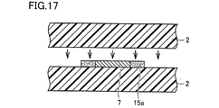
ここまでの処理を行なった樹脂シートを積み重ねる。一例として、ある1つの第1種導体パターン7の近傍の様子を図17に示す。矢印に示すように他の樹脂層2が上側から重ねられている。
積み重ねたものに対して熱圧着工程を行なう。これにより、導体パターンの外形線の一部または全部に沿って配置されていた樹脂ペーストは熱および圧力によって変形して、図18に示すように、樹脂層同士の隙間または導体パターンと樹脂層との隙間を埋める形で樹脂部15となる。このとき、樹脂部15は液体成分が実質的に残留していない状態である。そして、積層体1は一体化し、樹脂多層基板が得られる。なお、この変形によって、第1種導体パターン7の端部に樹脂ペーストの一部が被さった場合であっても、樹脂ペーストが流動して第1種導体パターン7の外形線の外側に流れる。また、各樹脂シートは樹脂層2となる。導体ビアを形成していた導電体ペーストは固化し、導体ビアとして出来上がる。
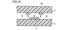
図15および図17では、樹脂層2の表面に第1種導体パターン7が形成され、この第1種導体パターン7を囲むように樹脂ペースト15aが配置されていたが、このような方法に限らず、図19に示すような方法であってもよい。すなわち、樹脂層2の表面に第1種導体パターン7が形成され、この第1種導体パターン7が形成されている樹脂層2の表面ではなく、他の樹脂層2の表面に樹脂ペースト15aが配置されている。樹脂ペースト15aは、第1種導体パターン7の外形線に対応した形状で配置されている。図19に示すように、第1種導体パターン7が配置された第1の樹脂層2と、樹脂ペースト15aが配置された第2の樹脂層2とを重ね合わせて熱圧着することによって、図18に示すような状態を得ることができる。このような方法を採用してもよい。
(実施の形態6)
図20を参照して、本発明に基づく実施の形態6における樹脂多層基板について説明する。本実施の形態における樹脂多層基板131の断面図を図20に示す。樹脂多層基板131は、部品3を備える。樹脂多層基板131は、導体ビア第1種接合部17と、導体ビア第2種接合部18とを備える。
図20を参照して、本発明に基づく実施の形態6における樹脂多層基板について説明する。本実施の形態における樹脂多層基板131の断面図を図20に示す。樹脂多層基板131は、部品3を備える。樹脂多層基板131は、導体ビア第1種接合部17と、導体ビア第2種接合部18とを備える。
樹脂多層基板131は、熱可塑性樹脂を主材料とする複数の樹脂層2を積層したものである積層体1と、積層体1に内蔵された部品3と、積層体1の内部において複数の樹脂層2のいずれかを貫通するように配置された導体ビア同士が積層体1の積層方向に沿って連なるように接合している部分であり、積層体1の積層方向の一方から見たとき接合面の外形線を有する1以上の導体ビア第1種接合部17と、積層体1の内部において複数の樹脂層2のいずれかを貫通するように配置された導体ビア同士が積層体1の積層方向に沿って連なるように接合している部分であり、積層体1の積層方向の一方から見たとき接合面の外形線を有する1以上の導体ビア第2種接合部18とを備える。導体ビア第1種接合部17においては、導体ビア6aと導体ビア6bとが互いに接合している。導体ビア6aは、図20における上方にいくほど径が大きくなるテーパ形状を有している。導体ビア6bは、図20における下方にいくほど径が大きくなるテーパ形状を有している。導体ビア第1種接合部17においては、導体ビア6aの径が大きい方の端面と、導体ビア6bの径が大きい方の端面とが向かい合って接合している。導体ビア第2種接合部18においても同様である。
導体ビア第1種接合部17の各々の外形線の少なくとも一部は、積層体1の積層方向の一方から見たとき部品3と重なる位置にある。導体ビア第2種接合部18の各々の外形線は、積層体1の積層方向の一方から見たとき部品3と全く重ならない位置にある。導体ビア第1種接合部17の各々の外形線のうち部品3と重なる部分に沿って、導体ビア第1種接合部17の外側に隣接するように、熱可塑性樹脂の粉末、たとえば液晶ポリマーの粉末を主材料とする樹脂ペースト由来であり、この樹脂ペーストの液体成分が実質的に残留していない樹脂部15が配置されている。導体ビア第2種接合部18の各々の外形線に沿う部分には樹脂部15が配置されていない。
部品3と重なる部分においては、熱圧着工程における熱や圧力の伝達が部品3によっていくらか遮られるので、作用する熱や圧力が不十分となる可能性があり、その結果、導体ビア第1種接合部の近傍において樹脂層が未接合状態となる部分が生じるおそれがあるが、本実施の形態では、そのような部分に樹脂部15が配置されているので、樹脂部が導体ビア同士の接合部の外形線近傍の隙間を埋めることとなる。したがって、熱圧着工程におけるプレスの熱や圧力の作用が不十分となりがちな箇所における樹脂層間の未接合状態を解消することができる。
(実施の形態7)
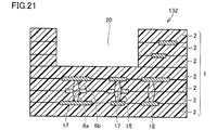
図21を参照して、本発明に基づく実施の形態7における樹脂多層基板について説明する。本実施の形態における樹脂多層基板132の断面図を図21に示す。樹脂多層基板132は、キャビティ20を備える。樹脂多層基板132は、導体ビア第1種接合部17と、導体ビア第2種接合部18とを備える。
図21を参照して、本発明に基づく実施の形態7における樹脂多層基板について説明する。本実施の形態における樹脂多層基板132の断面図を図21に示す。樹脂多層基板132は、キャビティ20を備える。樹脂多層基板132は、導体ビア第1種接合部17と、導体ビア第2種接合部18とを備える。
樹脂多層基板132は、熱可塑性樹脂を主材料とする複数の樹脂層2を積層したものである積層体1と、積層体1に積層方向に掘り下げるように設けられたキャビティ20と、積層体1の内部において複数の樹脂層2のいずれかを貫通するように配置された導体ビア同士が積層体1の積層方向に沿って連なるように接合している部分であり、積層体1の積層方向の一方から見たとき接合面の外形線を有する1以上の導体ビア第1種接合部17と、積層体1の内部において複数の樹脂層2のいずれかを貫通するように配置された導体ビア同士が積層体1の積層方向に沿って連なるように接合している部分であり、積層体1の積層方向の一方から見たとき接合面の外形線を有する1以上の導体ビア第2種接合部18とを備える。
導体ビア第1種接合部17の各々の外形線の少なくとも一部は、積層体1の積層方向の一方から見たときキャビティ20と重なる位置にあり、導体ビア第2種接合部18の各々の外形線は、積層体1の積層方向の一方から見たときキャビティ20と全く重ならない位置にある。導体ビア第1種接合部17の各々の外形線のうちキャビティ20と重なる部分に沿って、導体ビア第1種接合部17の外側に隣接するように、熱可塑性樹脂の粉末、たとえば液晶ポリマーの粉末を主材料とする樹脂ペースト由来であり、前記樹脂ペーストの液体成分が実質的に残留していない樹脂部15が配置されている。導体ビア第2種接合部18の各々の外形線に沿う部分には樹脂部15が配置されていない。
キャビティ20と重なる部分においては、熱圧着工程において熱や圧力の作用が不十分となる可能性があり、その結果、導体ビア第1種接合部の近傍において樹脂層が未接合状態となる部分が生じるおそれがあるが、本実施の形態では、そのような部分に樹脂部15が配置されているので、樹脂部が導体ビア同士の接合部の外形線近傍の隙間を埋めることとなる。したがって、熱圧着工程におけるプレスの熱や圧力の作用が不十分となりがちな箇所における樹脂層間の未接合状態を解消することができる。
(実施の形態8)
図22を参照して、本発明に基づく実施の形態8における樹脂多層基板について説明する。本実施の形態における樹脂多層基板141の断面図を図22に示す。樹脂多層基板141は、第1導体箔25を備える。樹脂多層基板141は、導体ビア第1種接合部17と、導体ビア第2種接合部18とを備える。
図22を参照して、本発明に基づく実施の形態8における樹脂多層基板について説明する。本実施の形態における樹脂多層基板141の断面図を図22に示す。樹脂多層基板141は、第1導体箔25を備える。樹脂多層基板141は、導体ビア第1種接合部17と、導体ビア第2種接合部18とを備える。
樹脂多層基板141は、熱可塑性樹脂を主材料とする複数の樹脂層2を積層したものである積層体1と、積層体1に内蔵された第1導体箔25と、積層体1の内部において複数の樹脂層2のいずれかを貫通するように配置された導体ビア同士が積層体1の積層方向に沿って連なるように接合している部分であり、積層体1の積層方向の一方から見たとき接合面の外形線を有する1以上の導体ビア第1種接合部17と、積層体1の内部において複数の樹脂層2のいずれかを貫通するように配置された導体ビア同士が積層体1の積層方向に沿って連なるように接合している部分であり、積層体1の積層方向の一方から見たとき接合面の外形線を有する1以上の導体ビア第2種接合部とを備える。
第1導体箔25は、積層体1の内部に存在するいずれの導体箔よりも厚い。導体ビア第1種接合部17の各々の外形線の少なくとも一部は、積層体1の積層方向の一方から見たとき第1導体箔25と重なる位置にある。導体ビア第2種接合部18の各々の外形線は、積層体1の積層方向の一方から見たとき第1導体箔25と全く重ならない位置にある。
導体ビア第1種接合部17の各々の外形線のうち第1導体箔25と重なる部分に沿って、導体ビア第1種接合部17の外側に隣接するように、熱可塑性樹脂の粉末、たとえば液晶ポリマーの粉末を主材料とする樹脂ペースト由来であり、この樹脂ペーストの液体成分が実質的に残留していない樹脂部15が配置されている。導体ビア第2種接合部18の各々の外形線に沿う部分には樹脂部15が配置されていない。
第1導体箔25と重なる部分においては、第1種導体箔25の厚みが厚く、この部分の剛性が相対的に高くなるので、熱圧着工程において積層体の形状に沿った変形が起こりにくくなる。これにより、熱圧着工程において作用する熱や圧力が不十分となる可能性があり、その結果、導体ビア第1種接合部の近傍において未接合状態の部分が生じるおそれがあるが、本実施の形態では、そのような部分に樹脂部15が配置されているので、樹脂部が導体ビア同士の接合部の外形線近傍の隙間を埋めることとなる。したがって、熱圧着工程におけるプレスの熱や圧力の作用が不十分となりがちな箇所における樹脂層間の未接合状態を解消することができる。
(変形例)
本実施の形態における樹脂多層基板の変形例として、図23に示すようなものも考えられる。図23には樹脂多層基板142が示される。樹脂多層基板142においては、同一層に並ぶ複数の導体ビア第1種接合部17をつなぐように樹脂部15が配置されている。このような構成であってもよい。
本実施の形態における樹脂多層基板の変形例として、図23に示すようなものも考えられる。図23には樹脂多層基板142が示される。樹脂多層基板142においては、同一層に並ぶ複数の導体ビア第1種接合部17をつなぐように樹脂部15が配置されている。このような構成であってもよい。
樹脂層2の主材料である熱可塑性樹脂は液晶ポリマーであり、樹脂部15の熱可塑性樹脂は液晶ポリマーであることが好ましい。この構成を採用することにより、熱圧着の際の樹脂層2と樹脂部15との密着性が高まる。樹脂層2の主材料である液晶ポリマーと、樹脂部15の液晶ポリマーとは、実質的に同種の液晶ポリマー材料からなることが好ましい。この構成を採用することにより、積層体1の中の樹脂層2および樹脂部15が同種の液晶ポリマー材料によって構成されるので、積層体の絶縁体部分の特性の場所によるばらつきを抑えることができる。
なお、上記実施の形態のうち複数を適宜組み合わせて採用してもよい。
なお、今回開示した上記実施の形態はすべての点で例示であって制限的なものではない。本発明の範囲は請求の範囲によって示され、請求の範囲と均等の意味および範囲内でのすべての変更を含むものである。
なお、今回開示した上記実施の形態はすべての点で例示であって制限的なものではない。本発明の範囲は請求の範囲によって示され、請求の範囲と均等の意味および範囲内でのすべての変更を含むものである。
1 積層体、2 樹脂層、3 部品、4 電極、6,6a,6b 導体ビア、7 第1種導体パターン、8 第2種導体パターン、11,12 導体パターン、15 樹脂部、17 導体ビア第1種接合部、18 導体ビア第2種接合部、20 キャビティ、25 第1導体箔、101,102,103,111,112,121,122,123,124,131,132,141,142 樹脂多層基板。
Claims (8)
- 熱可塑性樹脂を主材料とする複数の樹脂層を積層したものである積層体と、
前記積層体に内蔵された部品と、
前記積層体の内部で前記樹脂層同士の隙間に配置され、前記積層体の積層方向の一方から見たとき外形線を有する1以上の第1種導体パターンと、
前記積層体の内部で前記樹脂層同士の隙間に配置され、前記積層体の積層方向の一方から見たとき外形線を有する1以上の第2種導体パターンとを備え、
前記第1種導体パターンの各々の外形線の少なくとも一部は、前記積層体の積層方向の一方から見たとき前記部品と重なる位置にあり、
前記第2種導体パターンの各々の外形線は、前記積層体の積層方向の一方から見たとき前記部品と全く重ならない位置にあり、
前記第1種導体パターンの各々の外形線のうち前記部品と重なる部分に沿って、前記第1種導体パターンの外側に隣接するように、熱可塑性樹脂の粉末を主材料とする樹脂ペースト由来であり、前記樹脂ペーストの液体成分が実質的に残留していない樹脂部が配置されており、
前記第2種導体パターンの各々の外形線に沿う部分には前記樹脂部が配置されていない、樹脂多層基板。 - 熱可塑性樹脂を主材料とする複数の樹脂層を積層したものである積層体と、
前記積層体に積層方向に掘り下げるように設けられたキャビティと、
前記積層体の内部で前記樹脂層同士の隙間に配置され、前記積層体の積層方向の一方から見たとき外形線を有する1以上の第1種導体パターンと、
前記積層体の内部で前記樹脂層同士の隙間に配置され、前記積層体の積層方向の一方から見たとき外形線を有する1以上の第2種導体パターンとを備え、
前記第1種導体パターンの各々の外形線の少なくとも一部は、前記積層体の積層方向の一方から見たとき前記キャビティと重なる位置にあり、
前記第2種導体パターンの各々の外形線は、前記積層体の積層方向の一方から見たとき前記キャビティと全く重ならない位置にあり、
前記第1種導体パターンの各々の外形線のうち前記キャビティと重なる部分に沿って、前記第1種導体パターンの外側に隣接するように、熱可塑性樹脂の粉末を主材料とする樹脂ペースト由来であり、前記樹脂ペーストの液体成分が実質的に残留していない樹脂部が配置されており、
前記第2種導体パターンの各々の外形線に沿う部分には前記樹脂部が配置されていない、樹脂多層基板。 - 熱可塑性樹脂を主材料とする複数の樹脂層を積層したものである積層体と、
前記積層体に内蔵された第1導体箔と、
前記積層体の内部で前記樹脂層同士の隙間に配置され、前記積層体の積層方向の一方から見たとき外形線を有する1以上の第1種導体パターンと、
前記積層体の内部で前記樹脂層同士の隙間に配置され、前記積層体の積層方向の一方から見たとき外形線を有する1以上の第2種導体パターンとを備え、
前記第1導体箔は、前記1以上の第1種導体パターンおよび前記1以上の第2種導体パターンのいずれよりも厚く、
前記第1種導体パターンの各々の外形線の少なくとも一部は、前記積層体の積層方向の一方から見たとき前記第1導体箔と重なる位置にあり、
前記第2種導体パターンの各々の外形線は、前記積層体の積層方向の一方から見たとき前記第1導体箔と全く重ならない位置にあり、
前記第1種導体パターンの各々の外形線のうち前記第1導体箔と重なる部分に沿って、前記第1種導体パターンの外側に隣接するように、熱可塑性樹脂の粉末を主材料とする樹脂ペースト由来であり、前記樹脂ペーストの液体成分が実質的に残留していない樹脂部が配置されており、
前記第2種導体パターンの各々の外形線に沿う部分には前記樹脂部が配置されていない、樹脂多層基板。 - 熱可塑性樹脂を主材料とする複数の樹脂層を積層したものである積層体と、
前記積層体に内蔵された部品と、
前記積層体の内部において前記複数の樹脂層のいずれかを貫通するように配置された導体ビア同士が前記積層体の積層方向に沿って連なるように接合している部分であり、前記積層体の積層方向の一方から見たとき接合面の外形線を有する1以上の導体ビア第1種接合部と、
前記積層体の内部において前記複数の樹脂層のいずれかを貫通するように配置された導体ビア同士が前記積層体の積層方向に沿って連なるように接合している部分であり、前記積層体の積層方向の一方から見たとき接合面の外形線を有する1以上の導体ビア第2種接合部とを備え、
前記導体ビア第1種接合部の各々の外形線の少なくとも一部は、前記積層体の積層方向の一方から見たとき前記部品と重なる位置にあり、
前記導体ビア第2種接合部の各々の外形線は、前記積層体の積層方向の一方から見たとき前記部品と全く重ならない位置にあり、
前記導体ビア第1種接合部の各々の外形線のうち前記部品と重なる部分に沿って、前記導体ビア第1種接合部の外側に隣接するように、熱可塑性樹脂の粉末を主材料とする樹脂ペースト由来であり、前記樹脂ペーストの液体成分が実質的に残留していない樹脂部が配置されており、
前記導体ビア第2種接合部の各々の外形線に沿う部分には前記樹脂部が配置されていない、樹脂多層基板。 - 熱可塑性樹脂を主材料とする複数の樹脂層を積層したものである積層体と、
前記積層体に積層方向に掘り下げるように設けられたキャビティと、
前記積層体の内部において前記複数の樹脂層のいずれかを貫通するように配置された導体ビア同士が前記積層体の積層方向に沿って連なるように接合している部分であり、前記積層体の積層方向の一方から見たとき接合面の外形線を有する1以上の導体ビア第1種接合部と、
前記積層体の内部において前記複数の樹脂層のいずれかを貫通するように配置された導体ビア同士が前記積層体の積層方向に沿って連なるように接合している部分であり、前記積層体の積層方向の一方から見たとき接合面の外形線を有する1以上の導体ビア第2種接合部とを備え、
前記導体ビア第1種接合部の各々の外形線の少なくとも一部は、前記積層体の積層方向の一方から見たとき前記キャビティと重なる位置にあり、
前記導体ビア第2種接合部の各々の外形線は、前記積層体の積層方向の一方から見たとき前記キャビティと全く重ならない位置にあり、
前記導体ビア第1種接合部の各々の外形線のうち前記キャビティと重なる部分に沿って、前記導体ビア第1種接合部の外側に隣接するように、熱可塑性樹脂の粉末を主材料とする樹脂ペースト由来であり、前記樹脂ペーストの液体成分が実質的に残留していない樹脂部が配置されており、
前記導体ビア第2種接合部の各々の外形線に沿う部分には前記樹脂部が配置されていない、樹脂多層基板。 - 熱可塑性樹脂を主材料とする複数の樹脂層を積層したものである積層体と、
前記積層体に内蔵された第1導体箔と、
前記積層体の内部において前記複数の樹脂層のいずれかを貫通するように配置された導体ビア同士が前記積層体の積層方向に沿って連なるように接合している部分であり、前記積層体の積層方向の一方から見たとき接合面の外形線を有する1以上の導体ビア第1種接合部と、
前記積層体の内部において前記複数の樹脂層のいずれかを貫通するように配置された導体ビア同士が前記積層体の積層方向に沿って連なるように接合している部分であり、前記積層体の積層方向の一方から見たとき接合面の外形線を有する1以上の導体ビア第2種接合部とを備え、
前記第1導体箔は、前記積層体の内部に存在するいずれの導体箔よりも厚く、
前記導体ビア第1種接合部の各々の外形線の少なくとも一部は、前記積層体の積層方向の一方から見たとき前記第1導体箔と重なる位置にあり、
前記導体ビア第2種接合部の各々の外形線は、前記積層体の積層方向の一方から見たとき前記第1導体箔と全く重ならない位置にあり、
前記導体ビア第1種接合部の各々の外形線のうち前記第1導体箔と重なる部分に沿って、前記導体ビア第1種接合部の外側に隣接するように、熱可塑性樹脂の粉末を主材料とする樹脂ペースト由来であり、前記樹脂ペーストの液体成分が実質的に残留していない樹脂部が配置されており、
前記導体ビア第2種接合部の各々の外形線に沿う部分には前記樹脂部が配置されていない、樹脂多層基板。 - 前記樹脂層の主材料である熱可塑性樹脂は液晶ポリマーであり、前記樹脂部の熱可塑性樹脂は液晶ポリマーである、請求項1から6のいずれかに記載の樹脂多層基板。
- 前記樹脂層の主材料である液晶ポリマーと、前記樹脂部の液晶ポリマーとは、実質的に同種の液晶ポリマー材料からなる、請求項7に記載の樹脂多層基板。
Priority Applications (4)
| Application Number | Priority Date | Filing Date | Title |
|---|---|---|---|
| JP2018536056A JP6521186B2 (ja) | 2016-08-23 | 2017-04-28 | 樹脂多層基板 |
| CN201790001191.0U CN210124036U (zh) | 2016-08-23 | 2017-04-28 | 树脂多层基板 |
| US16/270,659 US10660219B2 (en) | 2016-08-23 | 2019-02-08 | Resin multilayer substrate |
| US16/846,774 US20200245473A1 (en) | 2016-08-23 | 2020-04-13 | Resin multilayer substrate |
Applications Claiming Priority (2)
| Application Number | Priority Date | Filing Date | Title |
|---|---|---|---|
| JP2016162632 | 2016-08-23 | ||
| JP2016-162632 | 2016-08-23 |
Related Child Applications (1)
| Application Number | Title | Priority Date | Filing Date |
|---|---|---|---|
| US16/270,659 Continuation US10660219B2 (en) | 2016-08-23 | 2019-02-08 | Resin multilayer substrate |
Publications (1)
| Publication Number | Publication Date |
|---|---|
| WO2018037628A1 true WO2018037628A1 (ja) | 2018-03-01 |
Family
ID=61245400
Family Applications (1)
| Application Number | Title | Priority Date | Filing Date |
|---|---|---|---|
| PCT/JP2017/016919 Ceased WO2018037628A1 (ja) | 2016-08-23 | 2017-04-28 | 樹脂多層基板 |
Country Status (4)
| Country | Link |
|---|---|
| US (2) | US10660219B2 (ja) |
| JP (2) | JP6521186B2 (ja) |
| CN (1) | CN210124036U (ja) |
| WO (1) | WO2018037628A1 (ja) |
Families Citing this family (1)
| Publication number | Priority date | Publication date | Assignee | Title |
|---|---|---|---|---|
| JP6521186B2 (ja) * | 2016-08-23 | 2019-05-29 | 株式会社村田製作所 | 樹脂多層基板 |
Citations (4)
| Publication number | Priority date | Publication date | Assignee | Title |
|---|---|---|---|---|
| JP2013123031A (ja) * | 2011-11-07 | 2013-06-20 | Denso Corp | 導電性材料および半導体装置 |
| WO2014103530A1 (ja) * | 2012-12-26 | 2014-07-03 | 株式会社村田製作所 | 部品内蔵基板 |
| WO2014109139A1 (ja) * | 2013-01-09 | 2014-07-17 | 株式会社村田製作所 | 樹脂多層基板およびその製造方法 |
| WO2014188830A1 (ja) * | 2013-05-22 | 2014-11-27 | 株式会社村田製作所 | フィブリル化液晶ポリマーパウダー、フィブリル化液晶ポリマーパウダーの製造方法、ペースト、樹脂多層基板、および、樹脂多層基板の製造方法 |
Family Cites Families (10)
| Publication number | Priority date | Publication date | Assignee | Title |
|---|---|---|---|---|
| US6281446B1 (en) * | 1998-02-16 | 2001-08-28 | Matsushita Electric Industrial Co., Ltd. | Multi-layered circuit board and method of manufacturing the same |
| JP4262967B2 (ja) * | 2001-11-29 | 2009-05-13 | 富士通株式会社 | 不良コンデンサのメッキ除去方法 |
| JP2008085310A (ja) * | 2006-08-28 | 2008-04-10 | Clover Denshi Kogyo Kk | 多層プリント配線基板 |
| US8278565B2 (en) * | 2008-01-18 | 2012-10-02 | Panasonic Corporation | Three-dimensional wiring board |
| JP5110164B2 (ja) * | 2008-07-17 | 2012-12-26 | 株式会社村田製作所 | 部品内蔵モジュール及びその製造方法 |
| CN102100132A (zh) * | 2008-07-17 | 2011-06-15 | 株式会社村田制作所 | 元器件内置模块的制造方法 |
| JP5533914B2 (ja) * | 2011-08-31 | 2014-06-25 | 株式会社デンソー | 多層基板 |
| WO2014054353A1 (ja) * | 2012-10-05 | 2014-04-10 | 株式会社村田製作所 | 電子部品内蔵モジュール及び通信端末装置 |
| JP2014225604A (ja) | 2013-05-17 | 2014-12-04 | 株式会社村田製作所 | 樹脂多層基板およびその製造方法 |
| JP6521186B2 (ja) * | 2016-08-23 | 2019-05-29 | 株式会社村田製作所 | 樹脂多層基板 |
-
2017
- 2017-04-28 JP JP2018536056A patent/JP6521186B2/ja active Active
- 2017-04-28 CN CN201790001191.0U patent/CN210124036U/zh active Active
- 2017-04-28 WO PCT/JP2017/016919 patent/WO2018037628A1/ja not_active Ceased
-
2019
- 2019-02-08 US US16/270,659 patent/US10660219B2/en active Active
- 2019-04-23 JP JP2019081948A patent/JP6729754B2/ja active Active
-
2020
- 2020-04-13 US US16/846,774 patent/US20200245473A1/en not_active Abandoned
Patent Citations (4)
| Publication number | Priority date | Publication date | Assignee | Title |
|---|---|---|---|---|
| JP2013123031A (ja) * | 2011-11-07 | 2013-06-20 | Denso Corp | 導電性材料および半導体装置 |
| WO2014103530A1 (ja) * | 2012-12-26 | 2014-07-03 | 株式会社村田製作所 | 部品内蔵基板 |
| WO2014109139A1 (ja) * | 2013-01-09 | 2014-07-17 | 株式会社村田製作所 | 樹脂多層基板およびその製造方法 |
| WO2014188830A1 (ja) * | 2013-05-22 | 2014-11-27 | 株式会社村田製作所 | フィブリル化液晶ポリマーパウダー、フィブリル化液晶ポリマーパウダーの製造方法、ペースト、樹脂多層基板、および、樹脂多層基板の製造方法 |
Also Published As
| Publication number | Publication date |
|---|---|
| US20190174639A1 (en) | 2019-06-06 |
| JP6729754B2 (ja) | 2020-07-22 |
| JP6521186B2 (ja) | 2019-05-29 |
| JP2019114820A (ja) | 2019-07-11 |
| CN210124036U (zh) | 2020-03-03 |
| JPWO2018037628A1 (ja) | 2019-06-20 |
| US20200245473A1 (en) | 2020-07-30 |
| US10660219B2 (en) | 2020-05-19 |
Similar Documents
| Publication | Publication Date | Title |
|---|---|---|
| JP5652481B2 (ja) | 樹脂多層基板およびその製造方法 | |
| JP5757376B1 (ja) | 多層基板の製造方法、多層基板および電磁石 | |
| WO2014109139A1 (ja) | 樹脂多層基板およびその製造方法 | |
| WO2012137626A1 (ja) | 部品内蔵樹脂基板およびその製造方法 | |
| JP5447735B2 (ja) | フレキシブル多層基板 | |
| JP2017050391A (ja) | 多層基板およびその製造方法 | |
| JP2011249745A (ja) | 多層基板 | |
| JP6696996B2 (ja) | 樹脂多層基板およびその製造方法 | |
| JP5962184B2 (ja) | 樹脂多層基板 | |
| JP6729754B2 (ja) | 樹脂多層基板の製造方法 | |
| JP5618001B2 (ja) | フレキシブル多層基板 | |
| JP6350758B2 (ja) | 樹脂多層基板およびその製造方法 | |
| JP5516830B2 (ja) | 部品内蔵樹脂基板 | |
| US9936575B2 (en) | Resin multilayer substrate and component module | |
| JP2013021126A (ja) | 多層基板の製造方法及び多層基板 | |
| JP5668866B2 (ja) | 部品内蔵樹脂基板 | |
| JP6323047B2 (ja) | 樹脂多層基板およびその製造方法 | |
| JP5618029B2 (ja) | 樹脂多層基板およびその製造方法 | |
| JP2011228471A (ja) | 多層基板とその製造方法 | |
| CN107889356A (zh) | 软硬复合线路板 | |
| JP5333634B2 (ja) | 多層基板の製造方法 | |
| WO2022030178A1 (ja) | 構造体およびその製造方法 | |
| WO2013002035A1 (ja) | 部品内蔵基板 | |
| WO2012124673A1 (ja) | 部品内蔵基板 | |
| JP2014222692A (ja) | 樹脂多層基板 |
Legal Events
| Date | Code | Title | Description |
|---|---|---|---|
| 121 | Ep: the epo has been informed by wipo that ep was designated in this application |
Ref document number: 17843117 Country of ref document: EP Kind code of ref document: A1 |
|
| ENP | Entry into the national phase |
Ref document number: 2018536056 Country of ref document: JP Kind code of ref document: A |
|
| NENP | Non-entry into the national phase |
Ref country code: DE |
|
| 122 | Ep: pct application non-entry in european phase |
Ref document number: 17843117 Country of ref document: EP Kind code of ref document: A1 |