WO2018020852A1 - 送信装置、送信方法、および通信システム - Google Patents
送信装置、送信方法、および通信システム Download PDFInfo
- Publication number
- WO2018020852A1 WO2018020852A1 PCT/JP2017/021337 JP2017021337W WO2018020852A1 WO 2018020852 A1 WO2018020852 A1 WO 2018020852A1 JP 2017021337 W JP2017021337 W JP 2017021337W WO 2018020852 A1 WO2018020852 A1 WO 2018020852A1
- Authority
- WO
- WIPO (PCT)
- Prior art keywords
- voltage
- driver
- switch
- output terminal
- signal
- Prior art date
Links
Images


Classifications
-
- H—ELECTRICITY
- H04—ELECTRIC COMMUNICATION TECHNIQUE
- H04L—TRANSMISSION OF DIGITAL INFORMATION, e.g. TELEGRAPHIC COMMUNICATION
- H04L25/00—Baseband systems
- H04L25/02—Details ; arrangements for supplying electrical power along data transmission lines
- H04L25/0264—Arrangements for coupling to transmission lines
- H04L25/028—Arrangements specific to the transmitter end
- H04L25/0284—Arrangements to ensure DC-balance
-
- H—ELECTRICITY
- H03—ELECTRONIC CIRCUITRY
- H03K—PULSE TECHNIQUE
- H03K19/00—Logic circuits, i.e. having at least two inputs acting on one output; Inverting circuits
- H03K19/0175—Coupling arrangements; Interface arrangements
- H03K19/0185—Coupling arrangements; Interface arrangements using field effect transistors only
-
- H—ELECTRICITY
- H03—ELECTRONIC CIRCUITRY
- H03K—PULSE TECHNIQUE
- H03K17/00—Electronic switching or gating, i.e. not by contact-making and –breaking
- H03K17/51—Electronic switching or gating, i.e. not by contact-making and –breaking characterised by the components used
- H03K17/56—Electronic switching or gating, i.e. not by contact-making and –breaking characterised by the components used by the use, as active elements, of semiconductor devices
- H03K17/687—Electronic switching or gating, i.e. not by contact-making and –breaking characterised by the components used by the use, as active elements, of semiconductor devices the devices being field-effect transistors
-
- H—ELECTRICITY
- H03—ELECTRONIC CIRCUITRY
- H03K—PULSE TECHNIQUE
- H03K19/00—Logic circuits, i.e. having at least two inputs acting on one output; Inverting circuits
- H03K19/0175—Coupling arrangements; Interface arrangements
-
- H—ELECTRICITY
- H03—ELECTRONIC CIRCUITRY
- H03K—PULSE TECHNIQUE
- H03K19/00—Logic circuits, i.e. having at least two inputs acting on one output; Inverting circuits
- H03K19/0175—Coupling arrangements; Interface arrangements
- H03K19/017545—Coupling arrangements; Impedance matching circuits
-
- H—ELECTRICITY
- H04—ELECTRIC COMMUNICATION TECHNIQUE
- H04B—TRANSMISSION
- H04B3/00—Line transmission systems
- H04B3/02—Details
- H04B3/04—Control of transmission; Equalising
- H04B3/06—Control of transmission; Equalising by the transmitted signal
-
- H—ELECTRICITY
- H04—ELECTRIC COMMUNICATION TECHNIQUE
- H04L—TRANSMISSION OF DIGITAL INFORMATION, e.g. TELEGRAPHIC COMMUNICATION
- H04L25/00—Baseband systems
- H04L25/02—Details ; arrangements for supplying electrical power along data transmission lines
- H04L25/026—Arrangements for coupling transmitters, receivers or transceivers to transmission lines; Line drivers
-
- H—ELECTRICITY
- H04—ELECTRIC COMMUNICATION TECHNIQUE
- H04L—TRANSMISSION OF DIGITAL INFORMATION, e.g. TELEGRAPHIC COMMUNICATION
- H04L25/00—Baseband systems
- H04L25/02—Details ; arrangements for supplying electrical power along data transmission lines
- H04L25/0264—Arrangements for coupling to transmission lines
- H04L25/0272—Arrangements for coupling to multiple lines, e.g. for differential transmission
-
- H—ELECTRICITY
- H04—ELECTRIC COMMUNICATION TECHNIQUE
- H04L—TRANSMISSION OF DIGITAL INFORMATION, e.g. TELEGRAPHIC COMMUNICATION
- H04L25/00—Baseband systems
- H04L25/02—Details ; arrangements for supplying electrical power along data transmission lines
- H04L25/0264—Arrangements for coupling to transmission lines
- H04L25/0278—Arrangements for impedance matching
-
- H—ELECTRICITY
- H04—ELECTRIC COMMUNICATION TECHNIQUE
- H04L—TRANSMISSION OF DIGITAL INFORMATION, e.g. TELEGRAPHIC COMMUNICATION
- H04L25/00—Baseband systems
- H04L25/02—Details ; arrangements for supplying electrical power along data transmission lines
- H04L25/0264—Arrangements for coupling to transmission lines
- H04L25/028—Arrangements specific to the transmitter end
-
- H—ELECTRICITY
- H04—ELECTRIC COMMUNICATION TECHNIQUE
- H04L—TRANSMISSION OF DIGITAL INFORMATION, e.g. TELEGRAPHIC COMMUNICATION
- H04L25/00—Baseband systems
- H04L25/02—Details ; arrangements for supplying electrical power along data transmission lines
- H04L25/03—Shaping networks in transmitter or receiver, e.g. adaptive shaping networks
- H04L25/03006—Arrangements for removing intersymbol interference
- H04L25/03012—Arrangements for removing intersymbol interference operating in the time domain
- H04L25/03019—Arrangements for removing intersymbol interference operating in the time domain adaptive, i.e. capable of adjustment during data reception
-
- H—ELECTRICITY
- H04—ELECTRIC COMMUNICATION TECHNIQUE
- H04L—TRANSMISSION OF DIGITAL INFORMATION, e.g. TELEGRAPHIC COMMUNICATION
- H04L25/00—Baseband systems
- H04L25/02—Details ; arrangements for supplying electrical power along data transmission lines
- H04L25/03—Shaping networks in transmitter or receiver, e.g. adaptive shaping networks
- H04L25/03006—Arrangements for removing intersymbol interference
- H04L25/03343—Arrangements at the transmitter end
-
- H—ELECTRICITY
- H04—ELECTRIC COMMUNICATION TECHNIQUE
- H04L—TRANSMISSION OF DIGITAL INFORMATION, e.g. TELEGRAPHIC COMMUNICATION
- H04L25/00—Baseband systems
- H04L25/38—Synchronous or start-stop systems, e.g. for Baudot code
- H04L25/40—Transmitting circuits; Receiving circuits
- H04L25/49—Transmitting circuits; Receiving circuits using code conversion at the transmitter; using predistortion; using insertion of idle bits for obtaining a desired frequency spectrum; using three or more amplitude levels ; Baseband coding techniques specific to data transmission systems
- H04L25/493—Transmitting circuits; Receiving circuits using code conversion at the transmitter; using predistortion; using insertion of idle bits for obtaining a desired frequency spectrum; using three or more amplitude levels ; Baseband coding techniques specific to data transmission systems by transition coding, i.e. the time-position or direction of a transition being encoded before transmission
-
- H—ELECTRICITY
- H03—ELECTRONIC CIRCUITRY
- H03K—PULSE TECHNIQUE
- H03K17/00—Electronic switching or gating, i.e. not by contact-making and –breaking
- H03K17/51—Electronic switching or gating, i.e. not by contact-making and –breaking characterised by the components used
- H03K17/56—Electronic switching or gating, i.e. not by contact-making and –breaking characterised by the components used by the use, as active elements, of semiconductor devices
- H03K17/687—Electronic switching or gating, i.e. not by contact-making and –breaking characterised by the components used by the use, as active elements, of semiconductor devices the devices being field-effect transistors
- H03K2017/6878—Electronic switching or gating, i.e. not by contact-making and –breaking characterised by the components used by the use, as active elements, of semiconductor devices the devices being field-effect transistors using multi-gate field-effect transistors
-
- H—ELECTRICITY
- H04—ELECTRIC COMMUNICATION TECHNIQUE
- H04L—TRANSMISSION OF DIGITAL INFORMATION, e.g. TELEGRAPHIC COMMUNICATION
- H04L25/00—Baseband systems
- H04L25/02—Details ; arrangements for supplying electrical power along data transmission lines
- H04L25/0264—Arrangements for coupling to transmission lines
- H04L25/0292—Arrangements specific to the receiver end
Definitions
- the present disclosure relates to a transmission device that transmits a signal, a transmission method used in such a transmission device, and a communication system including such a transmission device.
- Patent Documents 1 and 2 disclose a communication system that transmits three differential signals using three transmission paths.
- Patent Document 3 discloses a communication system that performs pre-emphasis.
- the first transmission device includes a voltage generation unit, a first driver, and a control unit.
- the voltage generation unit generates a predetermined voltage.
- the first driver has a first sub-driver and a second sub-driver.
- the first sub-driver is provided with a first switch provided on a path from the first power supply to the first output terminal, and a first switch provided on a path from the second power supply to the first output terminal. 2 and a third switch provided on the path from the voltage generation unit to the first output terminal, and the voltage state at the first output terminal is a predetermined number of voltage states of three or more. It can be set to either.
- the second sub-driver can adjust the voltage in each voltage state at the first output terminal.
- the control unit controls the operation of the first driver so as to perform emphasis.
- the second transmission device includes a driver unit, a control unit, and a voltage generation unit.
- the driver unit can transmit a data signal using a predetermined number of voltage states of 3 or more, and can set a voltage in each voltage state.
- the control unit causes the driver unit to perform emphasis by setting an emphasis voltage corresponding to a transition between a predetermined number of voltage states.
- the driver section includes a first switch provided on a path from the first power supply to the output terminal, a second switch provided on a path from the second power supply to the output terminal, and a voltage generation section. And a third switch provided on the path from the output terminal to the output terminal.
- a transmission method includes a first switch provided on a path from a first power supply to a first output terminal, and a path from the second power supply to the first output terminal.
- the communication system includes a transmission device and a reception device.
- the transmission device includes a voltage generation unit, a first driver, and a control unit.
- the voltage generation unit generates a predetermined voltage.
- the first driver has a first sub-driver and a second sub-driver.
- the first sub-driver is provided with a first switch provided on a path from the first power supply to the first output terminal, and a first switch provided on a path from the second power supply to the first output terminal. 2 and a third switch provided on the path from the voltage generation unit to the first output terminal, and the voltage state at the first output terminal is a predetermined number of voltage states of three or more. It can be set to either.
- the second sub-driver can adjust the voltage in each voltage state at the first output terminal.
- the control unit controls the operation of the first driver so as to perform emphasis.
- the voltage state at the first output terminal is selected from among a predetermined number of three or more voltage states by the first sub-driver. Set to either.
- the voltage in each voltage state at the first output terminal is adjusted by the second sub-driver.
- the first sub driver and the second sub driver are controlled to perform emphasis.
- the first sub-driver is provided with a first switch on a path from the first power supply to the first output terminal, and a second switch on the path from the second power supply to the first output terminal.
- a third switch is provided on the path from the voltage generator to the first output terminal.
- the data signal is transmitted using a predetermined number of voltage states of 3 or more. Then, emphasis is performed by setting an emphasis voltage corresponding to a transition between a predetermined number of voltage states.
- a first switch is provided on a path from the first power supply to the first output terminal, and a second switch is provided on a path from the second power supply to the first output terminal.
- a third switch is provided on the path from the voltage generator to the first output terminal.
- the first switch is provided on the path from the first power supply to the first output terminal, Since the second switch is provided on the path from the second power source to the first output terminal and the third switch is provided on the path from the voltage generator to the first output terminal, power consumption can be reduced. Can do.
- the effect described here is not necessarily limited, and there may be any effect described in the present disclosure.
- FIG. 1 is a block diagram illustrating a configuration example of a communication system according to an embodiment of the present disclosure. It is explanatory drawing showing the voltage state of the signal which the communication system shown in FIG. 1 transmits / receives. It is another explanatory drawing showing the voltage state of the signal which the communication system shown in Drawing 1 transmits and receives. It is explanatory drawing showing the transition of the symbol which the communication system shown in FIG. 1 transmits / receives.
- FIG. 2 is a block diagram illustrating a configuration example of a transmission unit illustrated in FIG. 1.
- 6 is a table illustrating an operation example of a transmission symbol generation unit illustrated in FIG. 5.
- FIG. 6 is a block diagram illustrating a configuration example of an output unit illustrated in FIG. 5.
- FIG. 1 is a block diagram illustrating a configuration example of a communication system according to an embodiment of the present disclosure. It is explanatory drawing showing the voltage state of the signal which the communication system shown in FIG. 1 transmits / receives. It is another explanatory drawing
- FIG. 8 is a block diagram illustrating a configuration example of a driver illustrated in FIG. 7.
- 8 is a table illustrating an operation example of the emphasis control unit illustrated in FIG. 7.
- FIG. 9 is an explanatory diagram illustrating an operation example of the driver illustrated in FIG. 8.
- FIG. 9 is an explanatory diagram illustrating another operation example of the driver illustrated in FIG. 8.
- FIG. 9 is an explanatory diagram illustrating another operation example of the driver illustrated in FIG. 8.
- FIG. 9 is an explanatory diagram illustrating another operation example of the driver illustrated in FIG. 8.
- FIG. 9 is an explanatory diagram illustrating another operation example of the driver illustrated in FIG. 8.
- FIG. 9 is an explanatory diagram illustrating another operation example of the driver illustrated in FIG. 8.
- FIG. 9 is an explanatory diagram illustrating another operation example of the driver illustrated in FIG. 8.
- FIG. 9 is an explanatory diagram illustrating another operation example of the driver illustrated in FIG. 8.
- FIG. 9 is an explanatory diagram illustrating another operation example of the driver illustrated in FIG. 8.
- FIG. 9 is an explanatory diagram illustrating another operation example of the driver illustrated in FIG. 8.
- FIG. 2 is a block diagram illustrating a configuration example of a receiving unit illustrated in FIG. 1.
- FIG. 14 is an explanatory diagram illustrating an example of a reception operation of the reception unit illustrated in FIG. 13.
- FIG. 8 is a waveform diagram illustrating an operation example of the transmission unit illustrated in FIG. 7.
- FIG. 9 is a schematic diagram illustrating an operation example of the driver illustrated in FIG. 8. It is a wave form diagram showing the other operation example of the transmission part shown in FIG. FIG.
- FIG. 9 is a schematic diagram illustrating another operation example of the driver illustrated in FIG. 8. It is a wave form diagram showing the other operation example of the transmission part shown in FIG.
- FIG. 9 is a schematic diagram illustrating an operation example of the driver illustrated in FIG. 8.
- FIG. 2 is a timing waveform diagram illustrating an operation example of the communication system illustrated in FIG. 1.
- FIG. 6 is a timing waveform diagram illustrating another operation example of the communication system illustrated in FIG. 1.
- FIG. 6 is a timing waveform diagram illustrating another operation example of the communication system illustrated in FIG. 1.
- FIG. 6 is a timing waveform diagram illustrating another operation example of the communication system illustrated in FIG. 1.
- FIG. 6 is a timing waveform diagram illustrating another operation example of the communication system illustrated in FIG. 1.
- FIG. 25 is a block diagram illustrating a configuration example of a driver illustrated in FIG. 24.
- FIG. 26 is an explanatory diagram illustrating an operation example of the driver illustrated in FIG. 25.
- FIG. 26 is an explanatory diagram illustrating another operation example of the driver illustrated in FIG. 25.
- FIG. 26 is an explanatory diagram illustrating another operation example of the driver illustrated in FIG. 25.
- FIG. 26 is an explanatory diagram illustrating another operation example of the driver illustrated in FIG. 25.
- FIG. 26 is an explanatory diagram illustrating another operation example of the driver illustrated in FIG.
- FIG. 26 is an explanatory diagram illustrating another operation example of the driver illustrated in FIG. 25.
- FIG. 26 is an explanatory diagram illustrating another operation example of the driver illustrated in FIG. 25.
- FIG. 26 is an explanatory diagram illustrating another operation example of the driver illustrated in FIG. 25.
- FIG. 26 is an explanatory diagram illustrating another operation example of the driver illustrated in FIG. 25.
- FIG. 26 is an explanatory diagram illustrating another operation example of the driver illustrated in FIG. 25.
- FIG. 33 is a block diagram illustrating a configuration example of an output unit illustrated in FIG. 32. It is explanatory drawing showing the voltage state of the signal which the communication system which concerns on another modification transmits / receives.
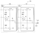
- 1 is a perspective view illustrating an external configuration of a smartphone to which a communication system according to an embodiment is applied. It is a block diagram showing the example of 1 structure of the application processor to which the communication system which concerns on one Embodiment was applied. 1 is a block diagram illustrating a configuration example of an image sensor to which a communication system according to an embodiment is applied. It is a block diagram which shows an example of a schematic structure of a vehicle control system.
- FIG. 1 illustrates a configuration example of a communication system (communication system 1) according to an embodiment.
- the communication system 1 is intended to improve communication performance by de-emphasis.
- the communication system 1 includes a transmission device 10, a transmission line 100, and a reception device 30.
- the transmitter 10 has three output terminals ToutA, ToutB, and ToutC
- the transmission line 100 has lines 110A, 110B, and 110C
- the receiver 30 has three input terminals TinA, TinB, and TinC. ing.
- the output terminal ToutA of the transmission device 10 and the input terminal TinA of the reception device 30 are connected to each other via a line 110A
- the output terminal ToutB of the transmission device 10 and the input terminal TinB of the reception device 30 are connected to each other via a line 110B.
- the output terminal ToutC of the transmission device 10 and the input terminal TinC of the reception device 30 are connected to each other via a line 110C.
- the characteristic impedance of the lines 110A to 110C is about 50 [ ⁇ ] in this example.
- the transmitter 10 outputs a signal SIGA from the output terminal ToutA, outputs a signal SIGB from the output terminal ToutB, and outputs a signal SIGC from the output terminal ToutC.
- the receiving device 30 receives the signal SIGA via the input terminal TinA, receives the signal SIGB via the input terminal TinB, and receives the signal SIGC via the input terminal TinC.
- the signals SIGA, SIGB, SIGC can take three voltage states SH, SM, SL, respectively.
- FIG. 2 shows three voltage states SH, SM, and SL.
- the voltage state SH is a state corresponding to three high-level voltages VH (VH0, VH1, VH2). Among the high level voltages VH0, VH1, and VH2, the high level voltage VH0 is the lowest voltage, and the high level voltage VH2 is the highest voltage.
- the voltage state SM is a state corresponding to three medium level voltages VM (VM0, VM1plus, VM1minus). Among the intermediate level voltages VM0, VM1plus, and VM1minus, the intermediate level voltage VM1minus is the lowest voltage, and the intermediate level voltage VM1plus is the highest voltage.
- the voltage state SL is a state corresponding to three low level voltages VL (VL0, VL1, VL2). Of the low level voltages VL0, VL1, and VL2, the low level voltage VL0 is the highest voltage, and the low level voltage VL2 is the lowest voltage.
- the high level voltage VH2 is a high level voltage when no de-emphasis is applied
- the medium level voltage VM0 is a medium level voltage when no de-emphasis is applied
- the low level voltage VL2 is a case where no de-emphasis is applied.
- the low level voltage is a case where no de-emphasis is applied.
- FIG. 3 shows voltage states of the signals SIGA, SIGB, and SIGC.
- the transmission apparatus 10 transmits six symbols “+ x”, “ ⁇ x”, “+ y”, “ ⁇ y”, “+ z”, and “ ⁇ z” using three signals SIGA, SIGB, and SIGC. For example, when transmitting the symbol “+ x”, the transmitter 10 sets the signal SIGA to the voltage state SH, the signal SIGB to the voltage state SL, and the signal SIGC to the voltage state SM. When transmitting the symbol “ ⁇ x”, the transmitting apparatus 10 sets the signal SIGA to the voltage state SL, the signal SIGB to the voltage state SH, and the signal SIGC to the voltage state SM.
- transmitting apparatus 10 When transmitting the symbol “+ y”, transmitting apparatus 10 sets signal SIGA to voltage state SM, signal SIGB to voltage state SH, and signal SIGC to voltage state SL.
- transmitting apparatus 10 sets signal SIGA to voltage state SM, signal SIGB to voltage state SL, and signal SIGC to voltage state SH.
- transmitting the symbol “+ z” the transmitter 10 sets the signal SIGA to the voltage state SL, the signal SIGB to the voltage state SM, and the signal SIGC to the voltage state SH.
- transmitting apparatus 10 sets the signal SIGA to the voltage state SH, the signal SIGB to the voltage state SM, and the signal SIGC to the voltage state SL.
- the transmission path 100 transmits a symbol sequence using such signals SIGA, SIGB, and SIGC. That is, the three lines 110A, 110B, and 110C function as one lane that conveys a sequence of symbols.
- the transmission device 10 includes a clock generation unit 11, a processing unit 12, and a transmission unit 20.
- the clock generation unit 11 generates a clock signal TxCK.
- the frequency of the clock signal TxCK is, for example, 2.5 [GHz].
- the present invention is not limited to this.
- the frequency of the clock signal TxCK can be set to 1.25 [GHz].
- the clock generation unit 11 is configured using, for example, a PLL (Phase Locked Loop), and generates a clock signal TxCK based on, for example, a reference clock (not shown) supplied from the outside of the transmission device 10.
- the clock generation unit 11 supplies the clock signal TxCK to the processing unit 12 and the transmission unit 20.
- the processing unit 12 generates transition signals TxF0 to TxF6, TxR0 to TxR6, TxP0 to TxP6 by performing predetermined processing.
- a set of transition signals TxF0, TxR0, and TxP0 indicate symbol transitions in a sequence of symbols transmitted by the transmission apparatus 10.
- a set of transition signals TxF1, TxR1, and TxP1 indicate symbol transitions
- a set of transition signals TxF2, TxR2, and TxP2 indicate symbol transitions
- a set of transition signals TxF3, TxR3, and TxP3 indicate symbol transitions.
- a transition is indicated, a set of transition signals TxF4, TxR4, TxP4 indicates a symbol transition, a set of transition signals TxF5, TxR5, TxP5 indicates a symbol transition, and a set of transition signals TxF6, TxR6, TxP6 are symbols It shows the transition. That is, the processing unit 12 generates seven sets of transition signals.
- transition signals TxF, TxR, and TxP are used as appropriate to represent any one of the seven sets of transition signals.
- FIG. 4 shows the relationship between the transition signals TxF, TxR, TxP and symbol transitions.
- the three-digit numerical value attached to each transition indicates the values of the transition signals TxF, TxR, and TxP in this order.
- the transition signal TxF (Flip) causes a symbol to transition between “+ x” and “ ⁇ x”, a symbol to transition between “+ y” and “ ⁇ y”, and “+ z” and “ ⁇ z”.
- the symbol is transitioned between. Specifically, when the transition signal TxF is “1”, the transition is performed so as to change the polarity of the symbol (for example, from “+ x” to “ ⁇ x”), and the transition signal TxF is “0”. In such a case, such a transition is not performed.
- the transition signals TxR (Rotation) and TxP (Polarity) are between “+ x” and other than “ ⁇ x” and between “+ y” and other than “ ⁇ y” when the transition signal TxF is “0”. , Symbol transition between “+ z” and other than “ ⁇ z”. Specifically, when the transition signals TxR and TxP are “1” and “0”, the transition is made clockwise (for example, from “+ x” to “+ y”) in FIG. 4 while maintaining the polarity of the symbol. When the transition signals TxR and TxP are “1” and “1”, the polarity of the symbol is changed and the transition is made clockwise (for example, from “+ x” to “ ⁇ y”) in FIG.
- transition signals TxR and TxP are “0” and “0”, transition is made counterclockwise in FIG. 4 while maintaining the polarity of the symbol (for example, from “+ x” to “+ z”).
- the signals TxR and TxP are “0” and “1”, the polarity of the symbol is changed, and the signal transitions counterclockwise in FIG. 4 (for example, from “+ x” to “ ⁇ z”).
- the processing unit 12 generates seven sets of such transition signals TxF, TxR, and TxP. Then, the processing unit 12 supplies the seven sets of transition signals TxF, TxR, TxP (transition signals TxF0 to TxF6, TxR0 to TxR6, TxP0 to TxP6) to the transmission unit 20.
- the transmission unit 20 generates signals SIGA, SIGB, and SIGC based on the transition signals TxF0 to TxF6, TxR0 to TxR6, and TxP0 to TxP6.
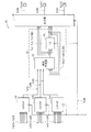
- FIG. 5 illustrates a configuration example of the transmission unit 20.
- the transmission unit 20 includes serializers 21F, 21R, and 21P, a transmission symbol generation unit 22, and an output unit 26.
- the serializer 21F serializes the transition signals TxF0 to TxF6 in this order based on the transition signals TxF0 to TxF6 and the clock signal TxCK to generate the transition signal TxF9.
- the serializer 21R serializes the transition signals TxR0 to TxR6 in this order based on the transition signals TxR0 to TxR6 and the clock signal TxCK to generate the transition signal TxR9.
- the serializer 21P serializes the transition signals TxP0 to TxP6 in this order based on the transition signals TxP0 to TxP6 and the clock signal TxCK to generate the transition signal TxP9.
- the transmission symbol generator 22 generates symbol signals Tx1, Tx2, Tx3 and symbol signals Dtx1, Dtx2, Dtx3 based on the transition signals TxF9, TxR9, TxP9 and the clock signal TxCK.
- the transmission symbol generation unit 22 includes a signal generation unit 23 and a flip-flop 24.
- the signal generator 23 generates symbol signals Tx1, Tx2, Tx3 related to the current symbol NS based on the transition signals TxF9, TxR9, TxP9 and the symbol signals Dtx1, Dtx2, Dtx3. Specifically, the signal generation unit 23, as illustrated in FIG. 4, based on the symbol (the previous symbol DS) indicated by the symbol signals Dtx1, Dtx2, and Dtx3 and the transition signals TxF9, TxR9, and TxP9. The current symbol NS is obtained and output as symbol signals Tx1, Tx2, Tx3.
- the flip-flop 24 samples the symbol signals Tx1, Tx2, and Tx3 based on the clock signal TxCK, and outputs the sampling results as symbol signals Dtx1, Dtx2, and Dtx3, respectively.
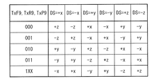
- FIG. 6 illustrates an operation example of the transmission symbol generation unit 22.
- FIG. 6 shows a symbol NS generated based on the symbol DS indicated by the symbol signals Dtx1, Dtx2, and Dtx3 and the transition signals TxF9, TxR9, and TxP9.
- a case where the symbol DS is “+ x” will be described as an example.
- the transition signals TxF9, TxR9, and TxP9 are “000”, the symbol NS is “+ z”, and when the transition signals TxF9, TxR9, and TxP9 are “001”, the symbol NS is “ ⁇ z”.
- the transition signals TxF9, TxR9, and TxP9 are “010”, the symbol NS is “+ y”.
- the symbol NS is “ If -y "and the transition signals TxF9, TxR9, TxP9 are" 1XX ", the symbol NS is" -x ".
- “X” indicates that either “1” or “0” may be used.
- the symbol DS is “ ⁇ x”, “+ y”, “ ⁇ y”, “+ z”, and “ ⁇ z”.
- the output unit 26 generates signals SIGA, SIGB, and SIGC based on the symbol signals Tx1, Tx2, Tx3, the symbol signals Dtx1, Dtx2, Dtx3, and the clock signal TxCK.
- FIG. 7 shows a configuration example of the output unit 26.
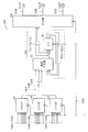
- the output unit 26 includes a voltage generation unit 50, driver control units 27N and 27D, emphasis control units 28A, 28B, and 28C, and drivers 29A, 29B, and 29C.
- the voltage generator 50 generates a voltage Vdc corresponding to the medium level voltage VM0.
- the voltage generation unit 50 includes a reference voltage generation unit 51, an operational amplifier 52, and a capacitive element 53.
- the reference voltage generation unit 51 includes, for example, a band gap reference circuit, and generates a reference voltage Vref corresponding to the medium level voltage VM0.
- a reference voltage Vref is supplied to the positive input terminal of the operational amplifier 52, and the negative input terminal is connected to the output terminal.
- the operational amplifier 52 operates as a voltage follower and outputs a voltage Vdc corresponding to the intermediate level voltage VM0.
- One end of the capacitive element 53 is connected to the output terminal of the operational amplifier 52, and the other end is grounded.
- the driver control unit 27N generates signals MAINAN, SUBAN, signals MAINBN, SUBBN, and signals MAINCN, SUBCN based on the symbol signals Tx1, Tx2, Tx3 related to the current symbol NS and the clock signal TxCK. Specifically, the driver control unit 27N obtains the voltage states of the signals SIGA, SIGB, and SIGC as shown in FIG. 3 based on the current symbol NS indicated by the symbol signals Tx1, Tx2, and Tx3.
- the driver control unit 27N sets the signals MAINAN and SUBAN to “1” and “0”, respectively, and when the signal SIGA is set to the voltage state SL, When MAINAN and SUBAN are set to “0” and “1”, respectively, and the signal SIGA is set to the voltage state SM, both the signals MAINAN and SUBAN are set to “1” or “0”. The same applies to the signals MAINBN and SUBBN and the signals MAINCN and SUBCN. Then, the driver control unit 27N supplies signals MAINAN and SUBAN to the emphasis control unit 28A, supplies signals MAINBN and SUBBN to the emphasis control unit 28B, and supplies signals MAINCN and SUBCN to the emphasis control unit 28C. Yes.
- the driver control unit 27D generates the signals MAINAD and SUBAD, the signals MAINBD and SUBBD, and the signals MAINCD and SUBCD based on the symbol signals Dtx1, Dtx2, and Dtx3 related to the previous symbol DS and the clock signal TxCK. is there.
- the driver control unit 27D has the same circuit configuration as the driver control unit 27N. Then, the driver control unit 27D supplies signals MAINAD and SUBAD to the emphasis control unit 28A, supplies signals MAINBD and SUBBD to the emphasis control unit 28B, and supplies signals MAINCD and SUBCD to the emphasis control unit 28C. Yes.
- the emphasis control unit 28A generates six signals UPA0, UPA1, MDA0, MDA1, DNA0, and DNA1 based on the signals MAINAN and SUBAN and the signals MAINAD and SUBAD.
- the driver 29A generates a signal SIGA based on the six signals UPA0, UPA1, MDA0, MDA1, DNA0, and DNA1.
- the emphasis control unit 28B generates six signals UPB0, UPB1, MDB0, MDB1, DNB0 and DNB1 based on the signals MAINBN and SUBBN and the signals MAINBD and SUBBD.
- the driver 29B generates a signal SIGB based on the six signals UPB0, UPB1, MDB0, MDB1, DNB0, and DNB1.
- the emphasis control unit 28C generates six signals UPC0, UPC1, MDC0, MDC1, DNC0, and DNC1 based on the signals MAINCN and SUBCN and the signals MAINCD and SUBCD.
- the driver 29C generates a signal SIGC based on the six signals UPC0, UPC1, MDC0, MDC1, DNC0, and DNC1.
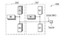
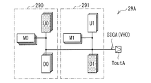
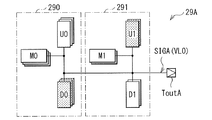
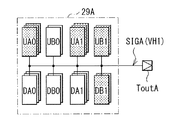
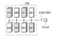
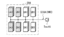
- FIG. 8 shows a configuration example of the driver 29A.
- the driver 29A has two sub-drivers 290 and 291.
- the sub-driver 290 includes M circuits U0 (circuits U0 1 to U0 M ), M circuits D0 (circuits D0 1 to D0 M ), and M circuits M0 (circuits M0 1 to M0 M ).
- the sub-driver 291 includes N circuits U1 (circuits U1 1 to U1 N ), N circuits D1 (circuits D1 1 to D1 N ), and N circuits M1 (circuits M1 1 to M1 N ).
- “M” is a number greater than “N”.
- the number of circuits U0, the number of circuits M0, the number of circuits D0, the number of circuits U1, the number of circuits M1, and the number of circuits D1 can be set separately.
- Each of the circuits U0 1 ⁇ U0 M, U1 1 ⁇ U1 N has a transistor 91, a resistance element 92.
- the transistor 91 is an N-channel MOS (Metal Oxide Semiconductor) FET (Field Effect Transistor).
- the signal UPA 0 is supplied to the gate of the transistor 91, the voltage V 1 is supplied to the drain, and the source is connected to one end of the resistance element 92.
- the signal UPA 1 is supplied to the gate of the transistor 91, the voltage V 1 is supplied to the drain, and the source is connected to one end of the resistance element 92.
- one end of the resistance element 92 is connected to the source of the transistor 91, and the other end is connected to the output terminal ToutA.
- the sum of the resistance value of the transistor 91 in the on state and the resistance value of the resistance element 92 is “50 ⁇ (M + N)” [ ⁇ ].
- Each of the circuits D 0 1 to D 0 M and D 1 1 to D 1 N has a resistance element 93 and a transistor 94.
- one end of the resistance element 93 is connected to the output terminal ToutA, and the other end is connected to the drain of the transistor 94.
- the transistor 94 is an N-channel MOS type FET.
- the signal DNA0 is supplied to the gate of the transistor 94, the drain is connected to the other end of the resistance element 93, and the source is grounded.
- the signal DNA1 is supplied to the gate of the transistor 94, the drain is connected to the other end of the resistance element 93, and the source is grounded.
- the sum of the resistance value of the resistance element 93 and the resistance value in the ON state of the transistor 94 is “50 ⁇ (M + N)” [ ⁇ ].
- Each of the circuits M0 1 to M0 M and M1 1 to M1 N includes a transistor 95 and a resistance element 96.
- the transistor 95 is an N-channel MOS type FET.
- the signal MDA0 is supplied to the gate of the transistor 95, the voltage Vdc generated by the voltage generator 50 is supplied to the source, and the drain is connected to one end of the resistor element 96.
- the signal MDA1 is supplied to the gate of the transistor 95, the voltage Vdc generated by the voltage generator 50 is supplied to the source, and the drain is connected to one end of the resistor element 96.
- one end of the resistance element 96 is connected to the drain of the transistor 95, and the other end is connected to the output terminal ToutA.
- the sum of the resistance value of the transistor 95 in the ON state and the resistance value of the resistance element 96 is “50 ⁇ (M + N)” [ ⁇ ] in this example.
- FIG. 9 illustrates an operation example of the emphasis control unit 28A.
- 10A to 10C schematically show an operation example of the driver 29A when the signal SIGA is set to the voltage state SH
- FIGS. 11A to 11C are diagrams of the driver 29A when the signal SIGA is set to the voltage state SM.
- FIGS. 12A to 12C schematically illustrate an operation example of the driver 29A when the signal SIGA is set to the voltage state SL.
- 10A to 10C, 11A to 11C, and 12A to 12C, among the circuits U0 1 to U0 M and U1 1 to U1 N the shaded circuit indicates a circuit in which the transistor 91 is turned on.
- a circuit that is not multiplied indicates a circuit in which the transistor 91 is in an off state.
- a shaded circuit indicates a circuit in which the transistor 94 is on, and a non-shaded circuit indicates that the transistor 94 is off.
- the circuit in a state is shown.
- the shaded circuit indicates a circuit in which the transistor 95 is on, and the non-shaded circuit indicates that the transistor 95 is in an off state.
- the circuit which becomes is shown.
- the emphasis control unit 28A and the driver 29A will be described as an example, but the same applies to the emphasis control unit 28B and the driver 29B, and the same applies to the emphasis control unit 28C and the driver 29C.
- the emphasis control unit 28A sets the voltage of the signal SIGA to three high level voltages as shown in FIGS. 10A to 10C. Set to one of VH0, VH1, and VH2.
- the emphasis control unit 28A has signals MAINAD and SUBAD related to the previous symbol DS of “0” and “1”, and relates to the current symbol NS.
- the signals MAINAN and SUBAN are “1” and “0”
- the signals UPA0, UPA1, MDA0, MDA1, DNA0, and DNA1 are set to “110000”.
- the driver 29A as shown in FIG. 10A, the transistors 91 in the circuits U0 1 to U0 M and U1 1 to U1 N are turned on.
- the voltage of the signal SIGA becomes the high level voltage VH2, and the output termination resistance (output impedance) of the driver 29A becomes about 50 [ ⁇ ].
- the emphasis control unit 28A has the signals MAINAD and SUBAD related to the previous symbol DS of “0” and “0”, and the signal MAINAN,
- the signals UPA0, UPA1, MDA0, MDA1, DNA0, and DNA1 are set to “100100”.
- the driver 29A as shown in FIG. 10B, the transistor 91 in the circuits U0 1 to U0 M is turned on, and the transistor 95 in the circuits M1 1 to M1 N is turned on.
- the voltage of the signal SIGA becomes the high level voltage VH1, and the output termination resistance (output impedance) of the driver 29A becomes about 50 [ ⁇ ].
- the signals MAINAD and SUBAD related to the previous symbol DS are “1” and “1”
- the signals MAINAN and SUBAN related to the current symbol NS are “1” and “0”.
- the emphasis control unit 28A has the signals MAINAD and SUBAD related to the previous symbol DS of “1” and “0”, and the signal MAINAN and the current symbol NS related to When SUBAN is “1” or “0”, the signals UPA0, UPA1, MDA0, MDA1, DNA0, and DNA1 are set to “100001”.
- the driver 29A as shown in FIG. 10C, the transistor 91 in the circuits U0 1 to U0 M is turned on, and the transistor 94 in the circuits D1 1 to D1 N is turned on.
- the voltage of the signal SIGA becomes the high level voltage VH0, and the output termination resistance (output impedance) of the driver 29A becomes about 50 [ ⁇ ].
- the emphasis control unit 28A sets the voltage of the signal SIGA to three as shown in FIGS. 11A to 11C. Set to any of medium level voltages VM0, VM1plus, VM1minus.
- the emphasis control unit 28A has signals MAINAD and SUBAD related to the previous symbol DS of “0” and “1”, and relates to the current symbol NS.
- the signals MAINAN and SUBAN are “0” and “0”
- the signals UPA0, UPA1, MDA0, MDA1, DNA0, and DNA1 are set to “011000”.
- the transistor 95 in the circuits M0 1 to M0 M is turned on, and the transistor 91 in the circuits U1 1 to U1 N is turned on.
- the voltage of the signal SIGA becomes the medium level voltage VM1plus, and the output termination resistance (output impedance) of the driver 29A becomes about 50 [ ⁇ ].
- the signals MAINAD and SUBAD related to the immediately preceding symbol DS are “0” and “1”
- the signals MAINAN and SUBAN related to the current symbol NS are “1” and “1”.
- the emphasis control unit 28A has the signals MAINAD and SUBAD related to the previous symbol DS of “0” and “0”, and the signal MAINAN,
- the signals UPA0, UPA1, MDA0, MDA1, DNA0, and DNA1 are set to “001100”.
- the driver 29A as shown in FIG. 11B, the transistors 95 in the circuits M0 1 to M0 M and M1 1 to M1 N are turned on.
- the voltage of the signal SIGA becomes the middle level voltage VM0, and the output termination resistance (output impedance) of the driver 29A becomes about 50 [ ⁇ ].
- the emphasis control unit 28A has the signals MAINAD and SUBAD related to the previous symbol DS of “1” and “0”, and the signal MAINAN and the current symbol NS related to When SUBAN is “0” or “0”, the signals UPA0, UPA1, MDA0, MDA1, DNA0, and DNA1 are set to “001001”.
- the driver 29A as shown in FIG. 11C, the transistors 95 in the circuits M0 1 to M0 M are turned on, and the transistors 94 in the circuits D1 1 to D1 N are turned on.
- the voltage of the signal SIGA becomes the medium level voltage VM1minus, and the output termination resistance (output impedance) of the driver 29A becomes about 50 [ ⁇ ].
- the signals MAINAD and SUBAD related to the previous symbol DS are “1” and “0”
- the signals MAINAN and SUBAN related to the current symbol NS are “1” and “1”.
- the emphasis control unit 28A reduces the voltage of the signal SIGA to three low values as shown in FIGS. 12A to 12C.
- the level voltage is set to any one of VL0, VL1, and VL2.
- the emphasis control unit 28A has signals MAINAD and SUBAD related to the previous symbol DS of “0” and “1”, and relates to the current symbol NS.
- the signals MAINAN and SUBAN are “0” and “1”
- the signals UPA0, UPA1, MDA0, MDA1, DNA0, and DNA1 are set to “010010”.
- the driver 29A as shown in FIG. 12A, the transistor 94 in the circuits D0 1 to D0 M is turned on, and the transistor 91 in the circuits U1 1 to U1 N is turned on.
- the voltage of the signal SIGA becomes the low level voltage VL0, and the output termination resistance (output impedance) of the driver 29A becomes about 50 [ ⁇ ].
- the emphasis control unit 28A has the signals MAINAD and SUBAD related to the previous symbol DS of “0” and “0”, and the signal MAINAN,
- the signals UPA0, UPA1, MDA0, MDA1, DNA0, and DNA1 are set to “000110”.
- the driver 29A as shown in FIG. 12B, the transistor 94 in the circuits D0 1 to D0 M is turned on, and the transistor 95 in the circuits M1 1 to M1 N is turned on.
- the voltage of the signal SIGA becomes the low level voltage VL1
- the output termination resistance (output impedance) of the driver 29A becomes about 50 [ ⁇ ].
- the signals MAINAD and SUBAD related to the previous symbol DS are “1” and “1”
- the signals MAINAN and SUBAN related to the current symbol NS are “0” and “1”.
- the emphasis control unit 28A has the signals MAINAD and SUBAD related to the previous symbol DS of “1” and “0”, and the signal MAINAN and the current symbol NS related to When SUBAN is “0” or “1”, the signals UPA0, UPA1, MDA0, MDA1, DNA0, and DNA1 are set to “000011”.
- the driver 29A as shown in FIG. 12C, the transistors 94 in the circuits D0 1 to D0 M and D1 1 to D1 N are turned on.
- the voltage of the signal SIGA becomes the low level voltage VL2, and the output termination resistance (output impedance) of the driver 29A becomes about 50 [ ⁇ ].
- the output unit 26 sets the voltages at the output terminals ToutA, ToutB, and ToutC based on the current symbol NS and the previous symbol DS.
- the transmission device 10 operates like a so-called 2-tap FIR (Finite Impulse Response) filter and performs a de-emphasis operation. Thereby, in the communication system 1, communication performance can be improved.
- 2-tap FIR Finite Impulse Response
- the reception device 30 includes a reception unit 40 and a processing unit 32.
- the receiving unit 40 receives the signals SIGA, SIGB, SIGC, and generates transition signals RxF, RxR, RxP and a clock signal RxCK based on the signals SIGA, SIGB, SIGC.
- FIG. 13 shows a configuration example of the receiving unit 40.
- the reception unit 40 includes resistance elements 41A, 41B, and 41C, switches 42A, 42B, and 42C, amplifiers 43A, 43B, and 43C, a clock generation unit 44, flip-flops 45 and 46, and a signal generation unit 47. is doing.
- the resistance elements 41A, 41B, and 41C function as termination resistors of the communication system 1, and the resistance value is about 50 [ ⁇ ] in this example.
- One end of the resistance element 41A is connected to the input terminal TinA and is connected to the positive input terminal of the amplifier 43A and the negative input terminal of the amplifier 43C, and the other end is connected to one end of the switch 42A.
- One end of the resistance element 41B is connected to the input terminal TinB and is connected to the positive input terminal of the amplifier 43B and the negative input terminal of the amplifier 43A, and the other end is connected to one end of the switch 42B.
- One end of the resistance element 41C is connected to the input terminal TinC and is connected to the positive input terminal of the amplifier 43C and the negative input terminal of the amplifier 43B, and the other end is connected to one end of the switch 42C.
- One end of the switch 42A is connected to the other end of the resistance element 41A, and the other end is connected to the other ends of the switches 42B and 42C.
- One end of the switch 42B is connected to the other end of the resistance element 41B, and the other end is connected to the other ends of the switches 42A and 42C.
- One end of the switch 42C is connected to the other end of the resistance element 41C, and the other end is connected to the other ends of the switches 42A and 42B.
- the switches 42A, 42B, and 42C are set to an on state, and the resistance elements 41A to 41C function as termination resistors.
- the positive input terminal of the amplifier 43A is connected to the negative input terminal of the amplifier 43C and one end of the resistance element 41A and to the input terminal TinA, and the negative input terminal is connected to the positive input terminal of the amplifier 43B and one end of the resistance element 41B. Connected to the input terminal TinB.
- the positive input terminal of the amplifier 43B is connected to the negative input terminal of the amplifier 43A and one end of the resistance element 41B and to the input terminal TinB, and the negative input terminal is connected to the positive input terminal of the amplifier 43C and one end of the resistance element 41C. Connected to the input terminal TinC.
- the positive input terminal of the amplifier 43C is connected to the negative input terminal of the amplifier 43B and one end of the resistance element 41C and to the input terminal TinC, and the negative input terminal is connected to the positive input terminal of the amplifier 43A and one end of the resistance element 41A. Connected to the input terminal TinA.
- the amplifier 43A outputs a signal corresponding to the difference AB (SIGA ⁇ SIGB) between the signal SIGA and the signal SIGB, and the amplifier 43B corresponds to the difference BC (SIGB ⁇ SIGC) between the signal SIGB and the signal SIGC.
- the amplifier 43C outputs a signal corresponding to the difference CA (SIGC-SIGA) between the signal SIGC and the signal SIGA.
- FIG. 14 illustrates an operation example of the amplifiers 43A, 43B, and 43C when the receiving unit 40 receives the symbol “+ x”.
- the switches 42A, 42B, and 42C are not shown because they are in the on state.
- the voltage state of the signal SIGA is the voltage state SH
- the voltage state of the signal SIGB is the voltage state SL
- the voltage state of the signal SIGC is the voltage state SM.
- the current Iin flows in the order of the input terminal TinA, the resistance element 41A, the resistance element 41B, and the input terminal TinB.
- the difference AB becomes positive (AB> 0).
- the amplifier 43A outputs “1”.
- the voltage corresponding to the voltage state SL is supplied to the positive input terminal of the amplifier 43B, and the voltage corresponding to the voltage state SM is supplied to the negative input terminal, so that the difference BC becomes negative (BC ⁇ 0).
- the amplifier 43B outputs “0”.
- the voltage corresponding to the voltage state SM is supplied to the positive input terminal of the amplifier 43C, and the voltage corresponding to the voltage state SH is supplied to the negative input terminal, so that the difference CA is negative (CA ⁇ 0).
- the amplifier 43C outputs “0”.
- the clock generator 44 generates a clock signal RxCK based on the output signals of the amplifiers 43A, 43B, and 43C.
- the flip-flop 45 delays the output signals of the amplifiers 43A, 43B, and 43C by one clock of the clock signal RxCK and outputs the delayed signals.
- the flip-flop 46 delays the three output signals of the flip-flop 45 by one clock of the clock signal RxCK and outputs each of them.
- the signal generator 47 generates transition signals RxF, RxR, RxP based on the output signals of the flip-flops 45, 46 and the clock signal RxCK. These transition signals RxF, RxR, and RxP correspond to the transition signals TxF9, TxR9, and TxP9 (FIG. 5) in the transmission apparatus 10, respectively, and represent symbol transitions.
- the signal generator 47 identifies symbol transitions (FIG. 4) based on the symbols indicated by the output signal of the flip-flop 45 and the symbols indicated by the output signal of the flip-flop 46, and generates the transition signals RxF, RxR, RxP. It is supposed to be.
- the processing unit 32 (FIG. 1) performs predetermined processing based on the transition signals RxF, RxR, RxP and the clock signal RxCK.
- the drivers 29A, 29B, and 29C respectively correspond to specific examples of “first driver”, “second driver”, and “third driver” in the present disclosure.
- the drivers 29A, 29B, and 29C correspond to a specific example of “driver unit” in the present disclosure.
- the sub driver 290 corresponds to a specific example of “first sub driver” in the present disclosure.
- the sub driver 291 corresponds to a specific example of “second sub driver” in the present disclosure.
- the transistor 91 of the sub-driver 290 corresponds to a specific example of “first switch” in the present disclosure, and the transistor 94 of the sub-driver 290 corresponds to a specific example of “second switch” in the present disclosure.
- the transistor 95 of the sub-driver 290 corresponds to a specific example of “third switch” in the present disclosure.
- the transistor 91 of the sub-driver 291 corresponds to a specific example of “fourth switch” in the present disclosure, and the transistor 94 of the sub-driver 291 corresponds to a specific example of “fifth switch” in the present disclosure.
- the transistor 95 of the sub-driver 291 corresponds to a specific example of “sixth switch” in the present disclosure.
- the emphasis control units 28A to 28C correspond to a specific example of “control unit” in the present disclosure.
- the transmission symbol generation unit 22 corresponds to a specific example of “signal generation unit” in the present disclosure.
- the voltage V1 supplied to the drain of the transistor 91 corresponds to a specific example of one of “first power supply” and “second power supply” in the present disclosure.
- the ground voltage supplied to the source of the transistor 94 corresponds to a specific example of the other of the “first power supply” and the “second power supply” in the present disclosure.
- the clock generation unit 11 of the transmission device 10 generates a clock signal TxCK.
- the processing unit 12 generates transition signals TxF0 to TxF6, TxR0 to TxR6, TxP0 to TxP6 by performing predetermined processing.
- the serializer 21F generates the transition signal TxF9 based on the transition signals TxF0 to TxF6 and the clock signal TxCK, and the serializer 21R generates the transition signal based on the transition signals TxR0 to TxR6 and the clock signal TxCK.
- TxR9 is generated, and the serializer 21P generates the transition signal TxP9 based on the transition signals TxP0 to TxP6 and the clock signal TxCK.
- the transmission symbol generation unit 22 Based on the transition signals TxF9, TxR9, TxP9 and the clock signal TxCK, the transmission symbol generation unit 22 performs symbol signals Tx1, Tx2, Tx3 related to the current symbol NS and symbol signals Dtx1, Dtx2 related to the previous symbol DS. , Dtx3.
- the voltage generation unit 50 generates a voltage Vdc having a voltage corresponding to the intermediate level voltage VM0.
- the driver control unit 27N generates signals MAINAN, SUBAN, MAINBN, SUBBN, MAINCN, and SUBCN based on the symbol signals Tx1, Tx2, and Tx3 related to the current symbol NS and the clock signal TxCK.
- the driver control unit 27D generates signals MAINAD, SUBAD, MAINBD, SUBBD, MAINCD, and SUBCD based on the symbol signals Dtx1, Dtx2, and Dtx3 related to the immediately preceding symbol DS and the clock signal TxCK.
- the emphasis control unit 28A generates signals UPA0, UPA1, MDA0, MDA1, DNA0, and DNA1 based on the signals MAINAN, SUBAN, MAINAD, and SUBAD.
- the emphasis control unit 28B generates signals UPB0, UPB1, MDB0, MDB1, DNB0, and DNB1 based on the signals MAINBN, SUBBN, MAINBD, and SUBBD.
- the emphasis control unit 28B generates signals UPC0, UPC1, MDC0, MDC1, DNC0, and DNC1 based on the signals MAINCN, SUBCN, MAINCD, and SUBCD.
- Driver 29A generates signal SIGA based on signals UPA0, UPA1, MDA0, MDA1, DNA0, and DNA1.
- Driver 29B generates signal SIGB based on signals UPB0, UPB1, MDB0, MDB1, DNB0, and DNB1.
- Driver 29C generates signal SIGC based on signals UPC0, UPC1, MDC0, MDC1, DNC0, and DNC1.
- receiving unit 40 receives signals SIGA, SIGB, and SIGC, and generates transition signals RxF, RxR, RxP and clock signal RxCK based on signals SIGA, SIGB, and SIGC. .
- the processing unit 32 performs predetermined processing based on the transition signals RxF, RxR, RxP and the clock signal RxCK.
- the output unit 26 of the transmission device 10 sets voltages at the output terminals ToutA, ToutB, and ToutC based on the current symbol NS and the previous symbol DS, respectively.
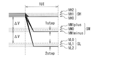
- FIG. 15 and 16 show the operation when the voltage state of the signal SIGA transitions from the voltage state SH to another voltage state.
- FIG. 15 shows the voltage change of the signal SIGA
- FIG. 16 shows the driver 29A. The transition of the operation state in is shown. The same applies to the signals SIGB and SIGC.
- 1 UI Unit Interval
- ⁇ V is a difference between the high level voltage VH0 and the intermediate level voltage VM0
- similarly, is a difference between the intermediate level voltage VM0 and the low level voltage VL0.
- the high level voltage VH0, the medium level voltage VM0, and the low level voltage VL0 are voltages that serve as a reference for the de-emphasis operation.
- the voltage of the signal SIGA is one of the three high-level voltages VH (VH0, VH1, VH2) as shown in FIG. Changes to a medium level voltage VM1minus.
- VH0, VH1, VH2 the voltage state in the preceding symbol DS is the voltage state SH
- the signals MAINAD and SUBAD are “1” and “0”
- the voltage state in the current symbol NS is Since the voltage state is SM, the signals MAINAN and SUBAN are, for example, “0” and “0”. Therefore, as shown in FIG.
- the emphasis control unit 28A sets the signals UPA0, UPA1, MDA0, MDA1, DNA0, and DNA1 to “001001”.
- the driver 29A as shown in FIG. 16, the transistor 95 in the circuits M0 1 to M0 M is turned on, and the transistor 94 in the circuits D1 1 to D1 N is turned on.
- the voltage of the signal SIGA becomes the middle level voltage VM1minus.
- the voltage of the signal SIGA is set to the medium level voltage VM1minus. That is, in this case, as shown in FIG. 15, since the transition amount of the signal SIGA is about ( ⁇ V), the emphasis control unit 28A uses the voltage after the transition of the signal SIGA as a reference medium.
- the medium level voltage VM1minus is set one step lower than the level voltage VM0.
- the voltage of the signal SIGA When the voltage state of the signal SIGA transitions from the voltage state SH to the voltage state SL, the voltage of the signal SIGA has three high level voltages VH (VH0, VH1, VH2) as shown in FIG. From one of the above to the low level voltage VL2. Specifically, in this case, since the voltage state in the preceding symbol DS is the voltage state SH, the signals MAINAD and SUBAD are “1” and “0”, and the voltage state in the current symbol NS is Since the voltage state is SL, the signals MAINAN and SUBAN are “0” and “1”. Therefore, as shown in FIG. 9, the emphasis control unit 28A sets the signals UPA0, UPA1, MDA0, MDA1, DNA0, and DNA1 to “000011”.
- the transistors 94 in the circuits D0 1 to D0 M and D1 1 to D1 N are turned on.
- the voltage of the signal SIGA becomes the low level voltage VL2.
- the voltage of the signal SIGA is set to the low level voltage VL2. That is, in this case, as shown in FIG. 15, since the transition amount of the signal SIGA is about ( ⁇ 2 ⁇ V), the emphasis control unit 28A uses the voltage after the transition of the signal SIGA as a reference low level.
- the low level voltage VL2 is set two steps lower than the level voltage VL0.
- the voltage of the signal SIGA is one of three high-level voltages VH (VH0, VH1, VH2) as shown in FIG. To the high level voltage VH0.
- the signals MAINAD and SUBAD are “1” and “0”
- the voltage state in the current symbol NS is Since it is in the voltage state SH, the signals MAINAN and SUBAN are “1” and “0”. Therefore, as shown in FIG. 9, the emphasis control unit 28A sets the signals UPA0, UPA1, MDA0, MDA1, DNA0, and DNA1 to “100001”.
- the transistor 91 in the circuits U0 1 to U0 M is turned on, and the transistor 94 in the circuits D1 1 to D1 N is turned on.
- the voltage of the signal SIGA becomes the high level voltage VH0.
- the voltage of the signal SIGA is set to the high level voltage VH0 in the second and subsequent unit intervals. . That is, the high level voltage VH0 is a de-emphasized voltage.
- FIG. 17 and 18 show the operation when the voltage state of the signal SIGA transitions from the voltage state SM to another voltage state, FIG. 17 shows the voltage change of the signal SIGA, and FIG. 18 shows the driver 29A. The transition of the operation state in is shown.
- the voltage of the signal SIGA is one of the three medium level voltages VM (VM0, VM1plus, VM1minus) as shown in FIG. To the high level voltage VH1.
- the signals MAINAD and SUBAD are, for example, “0” and “0”, and the voltage state in the current symbol NS.
- the signals MAINAN and SUBAN are “1” and “0”. Therefore, as shown in FIG. 9, the emphasis control unit 28A sets the signals UPA0, UPA1, MDA0, MDA1, DNA0, and DNA1 to “100100”.
- the transistor 91 in the circuits U0 1 to U0 M is turned on, and the transistor 95 in the circuits M1 1 to M1 N is turned on.
- the voltage of the signal SIGA becomes the high level voltage VH1.
- the voltage of the signal SIGA is set to the high level voltage VH1. That is, in this case, as shown in FIG. 17, since the transition amount of the signal SIGA is about (+ ⁇ V), the emphasis control unit 28A uses the voltage after the transition of the signal SIGA as a reference high level.
- the high level voltage VH1 is set one step higher than the voltage VH0.
- the voltage of the signal SIGA transitions from the voltage state SM to the voltage state SL
- the voltage of the signal SIGA has three medium level voltages VM (VM0, VM1plus, VM1minus) as shown in FIG. From one of the above to the low level voltage VL1.
- the signals MAINAD and SUBAD are, for example, “0” and “0”
- the voltage state in the current symbol NS are “0” and “1”. Therefore, as shown in FIG.
- the emphasis control unit 28A sets the signals UPA0, UPA1, MDA0, MDA1, DNA0, and DNA1 to “000110”.
- the driver 29A as shown in FIG. 18, the transistor 94 in the circuits D0 1 to D0 M is turned on, and the transistor 95 in the circuits M1 1 to M1 N is turned on.
- the voltage of the signal SIGA becomes the low level voltage VL1.
- the voltage of the signal SIGA is set to the low level voltage VL1. That is, in this case, as shown in FIG. 17, since the transition amount of the signal SIGA is about ( ⁇ V), the emphasis control unit 28A uses the voltage after the transition of the signal SIGA as a reference low level.
- the low level voltage VL1 is set one step lower than the level voltage VL0.
- the voltage of the signal SIGA is one of three medium level voltages VM (VM0, VM1plus, VM1minus) as shown in FIG. To the middle level voltage VM0.
- the signals MAINAD and SUBAD are, for example, “0” and “0”
- the voltage state in the current symbol NS Is in the voltage state SM
- the signals MAINAN and SUBAN are, for example, “0” and “0”. Therefore, as shown in FIG.
- the emphasis control unit 28A sets the signals UPA0, UPA1, MDA0, MDA1, DNA0, and DNA1 to “001100”, for example.
- the driver 29A as shown in FIG. 18, the transistors 95 in the circuits M0 1 to M0 M and M1 1 to M1 N are turned on.
- the voltage of the signal SIGA becomes the middle level voltage VM0.
- the voltage of the signal SIGA is set to the medium level voltage VM0 in the second and subsequent unit intervals. . That is, the intermediate level voltage VM0 is a de-emphasized voltage.
- FIG. 19 and 20 show the operation when the voltage state of the signal SIGA transitions from the voltage state SL to another voltage state, FIG. 19 shows the voltage change of the signal SIGA, and FIG. 20 shows the driver 29A. The transition of the operation state in is shown.
- the voltage of the signal SIGA is one of the three low level voltages VL (VL0, VL1, VL2) as shown in FIG.
- VL0, VL1, VL2 the voltage state in the preceding symbol DS is the voltage state SL
- the signals MAINAD and SUBAD are “0” and “1”
- the voltage state in the current symbol NS is Since the voltage state is SM, the signals MAINAN and SUBAN are, for example, “0” and “0”. Therefore, as shown in FIG. 9, the emphasis control unit 28A sets the signals UPA0, UPA1, MDA0, MDA1, DNA0, and DNA1 to “011000”.
- driver 29A As shown in FIG. 20, transistor 95 in circuits M0 1 to M0 M is turned on, and transistor 91 in circuits U1 1 to U1 N is turned on. As a result, the voltage of the signal SIGA becomes the middle level voltage VM1plus.
- the voltage of the signal SIGA when the voltage state of the signal SIGA transits from the voltage state SL to the voltage state SM, the voltage of the signal SIGA is set to the medium level voltage VM1plus. That is, in this case, as shown in FIG. 19, since the transition amount of the signal SIGA is about (+ ⁇ V), the emphasis control unit 28A uses the voltage after the transition of the signal SIGA as a reference medium level.
- the medium level voltage VM1plus is set one step higher than the voltage VM0.
- the voltage of the signal SIGA When the voltage state of the signal SIGA changes from the voltage state SL to the voltage state SH, the voltage of the signal SIGA has three low level voltages VL (VL0, VL1, VL2) as shown in FIG. From one of the above to the high level voltage VH2. Specifically, in this case, since the voltage state in the preceding symbol DS is the voltage state SL, the signals MAINAD and SUBAD are “0” and “1”, and the voltage state in the current symbol NS is Since it is in the voltage state SH, the signals MAINAN and SUBAN are “1” and “0”. Therefore, as shown in FIG. 9, the emphasis control unit 28A sets the signals UPA0, UPA1, MDA0, MDA1, DNA0, and DNA1 to “110000”.
- the transistors 91 in the circuits U0 1 to U0 M and U1 1 to U1 N are turned on.
- the voltage of the signal SIGA becomes the high level voltage VH2.
- the voltage of the signal SIGA is set to the high level voltage VH2. That is, in this case, as shown in FIG. 19, since the transition amount of the signal SIGA is about (+ 2 ⁇ V), the emphasis control unit 28A uses the voltage after the transition of the signal SIGA as a reference high level. A high level voltage VH2 that is two steps higher than the voltage VH0 is set.
- the voltage of the signal SIGA is one of three low level voltages VL (VL0, VL1, VL2) as shown in FIG. To the low level voltage VL0.
- the signals MAINAD and SUBAD are “0” and “1”
- the voltage state in the current symbol NS is Since the voltage state is SL, the signals MAINAN and SUBAN are “0” and “1”. Therefore, as shown in FIG. 9, the emphasis control unit 28A sets the signals UPA0, UPA1, MDA0, MDA1, DNA0, and DNA1 to “010010”.
- driver 29A As shown in FIG. 20, transistor 94 in circuits D0 1 to D0 M is turned on, and transistor 91 in circuits U1 1 to U1 N is turned on. As a result, the voltage of the signal SIGA becomes the low level voltage VL0. As described above, in the transmission device 10, when the voltage state of the signal SIGA is maintained at the voltage state SL over a plurality of unit intervals, the voltage of the signal SIGA is set to the low level voltage VL0 in the second and subsequent unit intervals. . That is, the low level voltage VL0 is a de-emphasized voltage.
- the transmission device 10 sets the post-transition voltage in each of the signals SIGA, SIGB, and SIGC in accordance with the voltage transition amount associated with the voltage state transition. Specifically, when the voltage state transitions to a state that is one higher, the transmission device 10 sets the voltage after the transition to one level from a reference voltage (for example, the medium level voltage VM0 or the high level voltage VH0). Set to a higher voltage. That is, in this case, the transmission apparatus 10 sets a positive emphasis voltage for one stage. In addition, when the voltage state transits to a state that is two higher, the transmission device 10 sets the voltage after the transition to a voltage that is two steps higher than a reference voltage (for example, the high level voltage VH0).
- a reference voltage for example, the medium level voltage VM0 or the high level voltage VH0
- the transmission apparatus 10 sets positive emphasis voltages for two stages.
- the transmitting apparatus 10 sets the voltage after the transition to a voltage that is one step lower than a reference voltage (for example, the medium level voltage VM0 or the low level voltage VL0). Set. That is, in this case, the transmitter 10 sets a negative emphasis voltage for one stage.
- the transmission device 10 sets the voltage to a voltage that is two steps lower than a reference voltage (for example, the low level voltage VL0). That is, in this case, the transmission apparatus 10 sets negative emphasis voltages for two stages.
- the transmission device 10 sets the emphasis voltage in each of the signals SIGA, SIGB, and SIGC in accordance with the voltage transition amount so as to be proportional to the transition amount.
- 21A to 21E show an example of the operation of the communication system 1 when the symbol changes from “+ x” to a symbol other than “+ x”.
- FIG. 21A shows the symbol from “+ x” to “ ⁇ x”.
- 21B shows a case where the symbol makes a transition from “+ x” to “+ y”
- FIG. 21C shows a case where the symbol makes a transition from “+ x” to “ ⁇ y”
- FIG. Indicates a case where the symbol transitions from “+ x” to “+ z”
- FIG. 21E illustrates a case where the symbol transitions from “+ x” to “ ⁇ z”.
- (A) shows waveforms of signals SIGA, SIGB, and SIGC at the output terminals ToutA, ToutB, and ToutC of the transmission apparatus 10, and (B) shows differences AB, BC,
- the waveform of CA is shown.
- a solid line indicates a waveform when the de-emphasis operation is performed, and a broken line indicates a waveform when the de-emphasis operation is not performed.
- the voltage of the signal SIGA before the transition is one of the three high level voltages VH (VH0, VH1, VH2), but in this figure, the voltage of the signal SIGA is set to the high level voltage VH0 for convenience of explanation. Yes.
- the voltage of the signal SIGB before the transition is the low level voltage VL0
- the voltage of the signal SIGC before the transition is the middle level voltage VM0.
- the signal SIGA changes from the high level voltage VH0 to the low level voltage VL2, and the signal SIGB changes to the low level voltage. From VL0 to the high level voltage VH2, the signal SIGC is maintained at the medium level voltage VM0. That is, since the transition amount of the signal SIGA is about ( ⁇ 2 ⁇ V), the transmission apparatus 10 sets the voltage of the signal SIGA to the low level voltage VL2 that is two steps lower than the reference low level voltage VL0.
- the transmission apparatus 10 sets the voltage of the signal SIGB to the high level voltage VH2 that is two steps higher than the reference high level voltage VH0.
- the transition amount of the difference AB (SIGA-SIGB) is about ( ⁇ 4 ⁇ V)
- the difference BC after the transition is obtained when the de-emphasis operation is not performed.
- the transition amount of the difference BC (SIGB ⁇ SIGC) is about (+ 2 ⁇ V)
- the difference BC after the transition is two steps higher than the case where the de-emphasis operation is not performed.
- the transition amount of the difference CA (SIGC-SIGA) is about (+ 2 ⁇ V)
- the difference CA after the transition is two steps higher than that in the case where the de-emphasis operation is not performed.
- the signal SIGA changes from the high level voltage VH0 to the medium level voltage VM1minus, and the signal SIGB changes to the low level voltage VL0.
- the signal SIGC changes from the medium level voltage VM0 to the low level voltage VL1. That is, since the transition amount of the signal SIGA is approximately ( ⁇ V), the transmission apparatus 10 sets the voltage of the signal SIGA to the middle level voltage VM1minus that is one step lower than the reference middle level voltage VM0.
- the transmission apparatus 10 sets the voltage of the signal SIGB to the high level voltage VH2 that is two steps higher than the reference high level voltage VH0. Further, since the transition amount of the signal SIGC is approximately ( ⁇ V), the transmission apparatus 10 sets the voltage of the signal SIGC to the low level voltage VL1 that is one step lower than the reference low level voltage VL0. At this time, as shown in FIG. 21B (B), since the transition amount of the difference AB (SIGA-SIGB) is about ( ⁇ 3 ⁇ V), the difference AB after the transition is obtained when the de-emphasis operation is not performed. Compared to 3 levels lower. Further, since the transition amount of the difference BC (SIGB ⁇ SIGC) is about (+ 3 ⁇ V), the difference BC after the transition is three steps higher than the case where the de-emphasis operation is not performed.
- the signal SIGA changes from the high level voltage VH0 to the intermediate level voltage VM1minus, and the signal SIGB changes to the low level voltage.
- the signal SIGC changes from the medium level voltage VM0 to the high level voltage VH1. That is, since the transition amount of the signal SIGA is approximately ( ⁇ V), the transmission apparatus 10 sets the voltage of the signal SIGA to the middle level voltage VM1minus that is one step lower than the reference middle level voltage VM0. Further, since the transition amount of the signal SIGC is approximately (+ ⁇ V), the transmission apparatus 10 sets the voltage of the signal SIGC to the high level voltage VH1 that is one step higher than the reference high level voltage VH0.
- the transition amount of the difference AB (SIGA-SIGB) is about ( ⁇ V), and therefore the difference AB after the transition is obtained when the de-emphasis operation is not performed.
- the transition amount of the difference BC (SIGB ⁇ SIGC) is about ( ⁇ V)
- the difference BC after the transition is one step lower than that in the case where the de-emphasis operation is not performed.
- the transition amount of the difference CA (SIGC-SIGA) is about (+ 2 ⁇ V)
- the difference CA after the transition is two steps higher than that in the case where the de-emphasis operation is not performed.
- the signal SIGA changes from the high level voltage VH0 to the low level voltage VL2, and the signal SIGB changes to the low level voltage VL0.
- the signal SIGC changes from the medium level voltage VM0 to the high level voltage VH1. That is, since the transition amount of the signal SIGA is about ( ⁇ 2 ⁇ V), the transmission apparatus 10 sets the voltage of the signal SIGA to the low level voltage VL2 that is two steps lower than the reference low level voltage VL0.
- the transmission apparatus 10 sets the voltage of the signal SIGB to the intermediate level voltage VM1plus that is one step higher than the reference intermediate level voltage VM0. Further, since the transition amount of the signal SIGC is approximately (+ ⁇ V), the transmission apparatus 10 sets the voltage of the signal SIGC to the high level voltage VH1 that is one step higher than the reference high level voltage VH0.
- the transition amount of the difference AB (SIGA-SIGB) is about ( ⁇ 3 ⁇ V)
- the difference AB after the transition is obtained when the de-emphasis operation is not performed. Compared to 3 levels lower.
- the transition amount of the difference CA (SIGC-SIGA) is about (+ 3 ⁇ V)
- the difference CA after the transition is three steps higher than when the de-emphasis operation is not performed.
- the signal SIGA When the symbol transitions from “+ x” to “ ⁇ z”, as shown in FIG. 21E (A), the signal SIGA is maintained at the high level voltage VH0, and the signal SIGB is changed from the low level voltage VL0 to the medium level voltage.
- the signal SIGC changes from the medium level voltage VM0 to the low level voltage VL1. That is, since the transition amount of the signal SIGB is approximately (+ ⁇ V), the transmission apparatus 10 sets the voltage of the signal SIGB to the intermediate level voltage VM1plus that is one step higher than the reference intermediate level voltage VM0. Further, since the transition amount of the signal SIGC is approximately ( ⁇ V), the transmission apparatus 10 sets the voltage of the signal SIGC to the low level voltage VL1 that is one step lower than the reference low level voltage VL0.
- the transition amount of the difference AB (SIGA-SIGB) is about ( ⁇ V), and therefore the difference AB after the transition is obtained when the de-emphasis operation is not performed.
- the transition amount of the difference BC (SIGB ⁇ SIGC) is about (+ 2 ⁇ V)
- the difference BC after the transition is two steps higher than the case where the de-emphasis operation is not performed.
- the transition amount of the difference CA (SIGC-SIGA) is about ( ⁇ V)
- the difference CA after the transition is one step lower than that in the case where the de-emphasis operation is not performed.
- the emphasis voltage is set in each of the signals SIGA, SIGB, and SIGC according to the voltage transition amount. That is, the transmission device 10 performs a de-emphasis operation on each of the signals SIGA, SIGB, and SIGC (single-end signal).
- the waveform quality can be improved for each of the signals SIGA, SIGB, and SIGC, the communication performance can be improved.
- the difference AB, BC, and CA which are differential signals, can be changed in voltage transition amount.
- the emphasis voltage is set accordingly.
- FIG. 22 illustrates an eye diagram of the difference AB between the signal SIGA and the signal SIGB, the difference BC between the signal SIGB and the signal SIGC, and the difference CA between the signal SIGC and the signal SIGA when the de-emphasis operation is performed.
- FIG. 23 shows an eye diagram of differences AB, BC, and CA when the de-emphasis operation is not performed.
- the eye opening can be widened by performing the de-emphasis operation as shown in FIGS. 22 and 23, and as a result, the communication performance can be improved. .
- the driver 29A when the driver 29A is provided with circuits M0 1 to M0 M and M1 1 to M1 M , for example, when the voltage state at the output terminal ToutA is set to the voltage state SM, the circuits M0 1 to M0 The M transistor 95 was turned on (FIGS. 11A to 11C).
- the transistors 91 of U1 1 to U1 N are turned on and set to the medium level voltage VM0 (FIG. 11B).
- M1 1 to M1 M transistors 95 are turned on and set to the intermediate level voltage VM1minus (FIG. 11C)
- D1 1 to D1 M transistors 94 are turned on.
- a communication system 1R according to the comparative example includes a transmission device 10R.
- the transmission device 10R includes a transmission unit 20R.
- This transmission unit 20R has an output unit 26R, similar to the transmission unit 20 (FIG. 5) according to the present embodiment.
- FIG. 24 illustrates a configuration example of the output unit 26R.
- the output unit 26R includes emphasis control units 28RA, 28RB, and 28RC, and drivers 29RA, 29RB, and 29RC.
- the emphasis control unit 28RA generates eight signals UPAA0, UPAB0, UPAA1, UPAB1, DNAA0, DNAB0, DNAA1, and DNAB1 based on the signals MAINAN and SUBAN and the signals MAINAD and SUBAD.
- the driver 29RA generates a signal SIGA based on the eight signals UPAA0, UPAB0, UPAA1, UPAB1, DNAA0, DNAB0, DNAA1, and DNAB1.
- FIG. 25 illustrates a configuration example of the driver 29RA.
- Driver 29RA includes a K-number of circuits UA0 (circuits UA0 1 ⁇ UA0 K), and L number of circuits UB0 (circuits UB0 1 ⁇ UB0 L), the K circuit UA1 and (circuits UA1 1 ⁇ UA1 K), L Circuits UB1 (circuits UB1 1 to UB1 L ), K circuits DA0 (circuits DA0 1 to DA0 K ), L circuits DB0 (circuits DB0 1 to DB0 L ), and K circuits DA1 ( Circuit DA1 1 to DA1 K ) and L circuits DB1 (circuits DB1 1 to DB1 L ).
- “K” is a larger number than “L”.
- the sum of the resistance value in the ON state of the transistor 91 and the resistance value of the resistance element 92 is “50 ⁇ (2 ⁇ K + 2 ⁇ L)” [ ⁇ ].
- Each of the circuits DA0 1 to DA0 K , DB0 1 to DB0 L , DA1 1 to DA1 K , DB1 1 to DB1 L is similar to the circuits D0 1 to D0 M and D1 1 to D1 N according to the present embodiment.
- a resistor element 93 and a transistor 94 are included.
- the signal DNAA0 is supplied to the gate of the transistor 94 in the circuits DA0 1 to DA0 K
- the signal DNAB0 is supplied to the gate of the transistor 94 in the circuits DB0 1 to DB0 L
- the gate of the transistor 94 in the circuits DA1 1 to DA1 K is supplied.
- the signal DNAB1 is supplied to the gates of the transistors 94 of the circuits DB1 1 to DB1 L.
- the sum of the resistance value of the resistance element 93 and the resistance value of the transistor 94 in the ON state is “50 ⁇ (2 ⁇ K + 2 ⁇ L)” [ ⁇ ].
- FIGS. 26A to 26C show an operation example of the driver 29RA when the signal SIGA is set to the voltage state SH
- FIGS. 27A to 27C are an operation example of the driver 29RA when the signal SIGA is set to the voltage state SM
- FIGS. 28A to 28C show an operation example of the driver 29RA when the signal SIGA is set to the voltage state SL.
- the transistor 94 in the circuits DA0 1 to DA0 K , DB0 1 to DB0 L , DA1 1 to DA1 K , DB1 1 to DB1 L Turn on the.
- the driver 29A sets the voltage at the output terminal ToutA by the Thevenin termination. Due to the Thevenin termination, a large amount of current flows due to the potential difference between the voltage V1 and the ground voltage.
- the series resistance value of the Thevenin termination is about 100 [ ⁇ ].
- the transistors 95 of the circuits M0 1 to M0 M and M1 1 to M1 M Turn on the. That is, the voltage at the output terminal ToutA is not set by the Thevenin termination, but the voltage at the output terminal ToutA is set by using the voltage Vdc generated by the voltage generator 50.
- the transistors 95 of the circuits M0 1 to M0 M are turned on and the transistor 91 of the circuits U1 1 to U1 M is turned on. Turn on the.
- the sub-driver 290 is provided with the circuits M0 1 to M0 M.
- the transistors of the circuits M0 1 to M0 M Since 95 is turned on, power consumption can be reduced.
- the sub driver 291 since the sub driver 291 sets the emphasis voltage by adjusting the voltage in each voltage state, the communication performance can be improved.
- the emphasis voltage is set according to the amount of voltage transition in each of the signals SIGA, SIGB, and SIGC, the waveform quality can be improved for each of the signals SIGA, SIGB, and SIGC. Communication performance can be improved.
- FIG. 29 illustrates a configuration example of the driver 39A according to the present modification.
- the driver 39A corresponds to the driver 29A according to the above embodiment.
- the driver 39 has two sub-drivers 390 and 391.
- the sub-drivers 390 and 391 are obtained by changing the connection between the transistor 91 and the resistance element 92 in the sub-drivers 290 and 291 (FIG. 8) according to the above embodiment.
- the circuits U0 1 ⁇ U0 M, U1 1 ⁇ U1 N to one end of the resistance element 92 is supplied with the voltage V1, the other end is connected to the drain of the transistor 91.
- the signal UPA0 is supplied to the gate of the transistor 91, the drain is connected to the other end of the resistance element 92, and the source is connected to the output terminal ToutA.
- the signal UPA1 is supplied to the gate of the transistor 91, the drain is connected to the other end of the resistance element 92, and the source is connected to the output terminal ToutA.
- FIG. 30 illustrates a configuration example of another driver 49A according to this modification.
- the driver 49A corresponds to the driver 29A according to the above embodiment.
- the driver 49A has two sub-drivers 490 and 491.
- the sub-driver 490 has M circuits C0 (circuits C0 1 to C0 M ).
- the sub-driver 491 has N circuits C1 (circuits C1 1 to C1 N ).
- Each of the circuits C0 1 to C0 M and C1 1 to C1 N has resistance elements 92 and 97 and transistors 91, 94, and 95.
- the circuits C0 1 to C0 M will be described.
- the voltage V1 is supplied to one end of the resistance element 92, and the other end is connected to the drain of the transistor 91.
- a signal UPA0 is supplied to the gate of the transistor 91, the drain is connected to the other end of the resistance element 92, and the source is connected to one end of the resistance element 97 and the output terminal ToutA.
- One end of the resistance element 97 is connected to the source of the transistor 91 and the output terminal ToutA, and the other end is connected to the drains of the transistors 94 and 95.
- the signal DNA0 is supplied to the gate of the transistor 94, the drain is connected to the other end of the resistance element 97 and the drain of the transistor 95, and the source is grounded.
- a signal MDA0 is supplied to the gate of the transistor 95, the voltage Vdc generated by the voltage generator 50 is supplied to the source, and the drain is connected to the other end of the resistance element 97 and the drain of the transistor 94.
- the circuits C1 1 to C1 N will be described.
- the signal UPA1 is supplied to the gate of the transistor 91.
- a signal DNA 1 is supplied to the gate of the transistor 94.
- a signal MDA 1 is supplied to the gate of the transistor 95. The rest is the same as the circuits C0 1 to C0 M.
- the resistance element 97 corresponds to the resistance elements 93 and 96 in the driver 29A (FIG. 8) according to the above embodiment. That is, for example, when the transistor 94 is turned on in the sub-driver 490, the resistance value of the resistance element 97 and the on-resistance of the transistor 94 constitute the output impedance of the sub-driver 490, and the transistor 95 is turned on. In this case, the resistance value of the resistance element 97 and the ON resistance of the transistor 95 constitute the output impedance of the sub driver 490. The same applies to the sub-driver 491. With this configuration, the driver 49A can reduce the number of elements, and as a result, the circuit area can be reduced.
- FIG. 31 shows a configuration example of another driver 59A according to this modification.
- the driver 59A corresponds to the driver 29A according to the above embodiment.
- the driver 59A has two sub-drivers 590 and 591.
- the sub-driver 590 has M circuits CC0 (circuits CC0 1 to CC0 M ).
- the sub-driver 491 has N circuits CC1 (circuits CC1 1 to CC1 N ).
- Each of the circuits CC0 1 to CC0 M and CC1 1 to CC1 N includes transistors 91, 94, and 95 and a resistance element 98.
- the circuits CC0 1 to CC0 M will be described.
- the signal UPA0 is supplied to the gate of the transistor 91
- the voltage V1 is supplied to the drain
- the source is connected to the drains of the transistors 94 and 95 and one end of the resistance element 98.
- the signal DNA0 is supplied to the gate of the transistor 94, the drain is connected to the source of the transistor 91, the drain of the transistor 95, and one end of the resistance element 98, and the source is grounded.
- a signal MDA0 is supplied to the gate of the transistor 95, the voltage Vdc generated by the voltage generation unit 50 is supplied to the source, and the drain is connected to the source of the transistor 91, the drain of the transistor 94, and one end of the resistance element 98. Yes.
- One end of the resistance element 98 is connected to the source of the transistor 91 and the drains of the transistors 94 and 95, and the other end is connected to the output terminal ToutA.
- the circuits CC1 1 to CC1 N will be described.
- the signal UPA1 is supplied to the gate of the transistor 91.
- a signal DNA 1 is supplied to the gate of the transistor 94.
- a signal MDA 1 is supplied to the gate of the transistor 95. The rest is the same as the circuits CC0 1 to CC0 M.
- the resistance element 98 corresponds to the resistance elements 92, 93, and 96 in the driver 29A (FIG. 8) according to the above embodiment. That is, for example, when the transistor 91 is turned on in the sub-driver 590, the resistance value of the resistance element 98 and the on-resistance of the transistor 91 constitute the output impedance of the sub-driver 590, and the transistor 94 is turned on. In this case, the resistance value of the resistance element 98 and the on-resistance of the transistor 94 constitute the output impedance of the sub-driver 590.
- the driver 59A can reduce the number of elements, and as a result, the circuit area can be reduced.
- the output unit 26 generates the signals SIGA, SIGB, and SIGC based on the symbol signals Tx1, Tx2, Tx3, the symbol signals Dtx1, Dtx2, Dtx3, and the clock signal TxCK.
- the present invention is not limited to this. It is not something.
- the transmitting apparatus 10A according to this modification will be described in detail.
- FIG. 32 illustrates a configuration example of the transmission unit 20A of the transmission device 10A.
- the transmission unit 20A includes a transmission symbol generation unit 22A and an output unit 26A.
- the transmission symbol generator 22A generates symbol signals Tx1, Tx2, Tx3 based on the transition signals TxF9, TxR9, TxP9 and the clock signal TxCK.
- the output unit 26A generates signals SIGA, SIGB, and SIGC based on the symbol signals Tx1, Tx2, Tx3 and the clock signal TxCK.
- FIG. 33 shows a configuration example of the output unit 26A.
- the output unit 26A includes a driver control unit 27N and flip-flops 17A, 17B, and 17C.
- the driver control unit 27N generates signals MAINAN, SUBAN, MAINBN, SUBBN, MAINCN, and SUBCN based on the symbol signals Tx1, Tx2, and Tx3 related to the current symbol NS and the clock signal TxCK.
- the flip-flop 17A delays the signals MAINAN and SUBAN by one clock of the clock signal TxCK, and outputs the delayed signals as signals MAINAD and SUBAD, respectively.
- the flip-flop 17B delays the signals MAINBN and SUBBN by one clock of the clock signal TxCK, and outputs the delayed signals as signals MAINBD and SUBBD, respectively.
- the flip-flop 17C delays the signals MAINCN and SUBCN by one clock of the clock signal TxCK, and outputs the delayed signals as signals MAINCD and SUBCD, respectively.
- FIG. 34 shows three voltage states SH, SM, and SL.
- the voltage state SH is a state corresponding to three high level voltages VH (VH0, VH1, VH2)
- the voltage state SM is a state corresponding to three medium level voltages VM (VM0, VM1plus, VM1minus)
- the voltage state SL is a state corresponding to three low level voltages VL (VL0, VL1, VL2).
- the high level voltage VH0 is a high level voltage when pre-emphasis is not applied
- the medium level voltage VM0 is a medium level voltage when pre-emphasis is not applied
- the low level voltage VL0 is not subjected to pre-emphasis.
- the low level voltage Even if comprised in this way, the effect similar to the case of the said embodiment can be acquired.
- FIG. 35 illustrates an appearance of a smartphone 300 (multifunctional mobile phone) to which the communication system of the above-described embodiment and the like is applied.
- Various devices are mounted on the smartphone 300, and the communication system according to the above-described embodiment is applied to a communication system that exchanges data between these devices.
- FIG. 36 illustrates a configuration example of the application processor 310 used in the smartphone 300.
- the application processor 310 includes a CPU (Central Processing Unit) 311, a memory control unit 312, a power supply control unit 313, an external interface 314, a GPU (Graphics Processing Unit) 315, a media processing unit 316, and a display control unit 317. And an MIPI (Mobile Industry Processor Interface) interface 318.
- the CPU 311, the memory control unit 312, the power supply control unit 313, the external interface 314, the GPU 315, the media processing unit 316, and the display control unit 317 are connected to the system bus 319, and data is mutually transmitted via the system bus 319. Can be exchanged.
- the CPU 311 processes various information handled by the smartphone 300 according to a program.
- the memory control unit 312 controls the memory 501 used when the CPU 311 performs information processing.
- the power supply control unit 313 controls the power supply of the smartphone 300.
- the external interface 314 is an interface for communicating with an external device, and is connected to the wireless communication unit 502 and the image sensor 410 in this example.
- the wireless communication unit 502 wirelessly communicates with a mobile phone base station, and includes, for example, a baseband unit, an RF (Radio Frequency) front end unit, and the like.
- the image sensor 410 acquires an image and includes, for example, a CMOS sensor.
- the GPU 315 performs image processing.
- the media processing unit 316 processes information such as voice, characters, and graphics.
- the display control unit 317 controls the display 504 via the MIPI interface 318.
- the MIPI interface 318 transmits an image signal to the display 504.
- As the image signal for example, a signal in YUV format or RGB format can be used.
- the MIPI interface 318 is operated based on a reference clock supplied from an oscillation circuit 330 including a crystal resonator, for example.
- the communication system between the MIPI interface 318 and the display 504 for example, the communication system of the above-described embodiment or the like is applied.
- FIG. 37 illustrates a configuration example of the image sensor 410.
- the image sensor 410 includes a sensor unit 411, an ISP (Image Signal Processor) 412, a JPEG (Joint Photographic Experts Group) encoder 413, a CPU 414, a RAM (Random Access Memory) 415, and a ROM (Read Only Memory) 416.
- Each of these blocks is connected to the system bus 420 in this example, and can exchange data with each other via the system bus 420.
- the sensor unit 411 acquires an image and is configured by, for example, a CMOS sensor.
- the ISP 412 performs predetermined processing on the image acquired by the sensor unit 411.
- the JPEG encoder 413 encodes an image processed by the ISP 412 to generate a JPEG format image.
- the CPU 414 controls each block of the image sensor 410 according to a program.
- the RAM 415 is a memory used when the CPU 414 performs information processing.
- the ROM 416 stores programs executed by the CPU 414, setting values obtained by calibration, and the like.
- the power supply control unit 417 controls the power supply of the image sensor 410.
- the I 2 C interface 418 receives a control signal from the application processor 310.
- the image sensor 410 receives a clock signal in addition to a control signal from the application processor 310. Specifically, the image sensor 410 is configured to operate based on clock signals having various frequencies.
- the MIPI interface 419 transmits an image signal to the application processor 310.
- As the image signal for example, a signal in YUV format or RGB format can be used.
- the MIPI interface 419 operates based on a reference clock supplied from an oscillation circuit 430 including a crystal resonator, for example.
- the communication system between the MIPI interface 419 and the application processor 310 for example, the communication system of the above-described embodiment or the like is applied.
- the technology according to the present disclosure can be applied to various products.
- the technology according to the present disclosure may be any type of movement such as an automobile, an electric vehicle, a hybrid electric vehicle, a motorcycle, a bicycle, personal mobility, an airplane, a drone, a ship, a robot, a construction machine, and an agricultural machine (tractor).
- FIG. 38 is a block diagram illustrating a schematic configuration example of a vehicle control system 7000 that is an example of a mobile control system to which the technology according to the present disclosure can be applied.
- the vehicle control system 7000 includes a plurality of electronic control units connected via a communication network 7010.
- the vehicle control system 7000 includes a drive system control unit 7100, a body system control unit 7200, a battery control unit 7300, a vehicle exterior information detection unit 7400, a vehicle interior information detection unit 7500, and an integrated control unit 7600. .
- the communication network 7010 for connecting the plurality of control units conforms to an arbitrary standard such as CAN (Controller Area Network), LIN (Local Interconnect Network), LAN (Local Area Network), or FlexRay (registered trademark). It may be an in-vehicle communication network.
- Each control unit includes a microcomputer that performs arithmetic processing according to various programs, a storage unit that stores programs executed by the microcomputer or parameters used for various calculations, and a drive circuit that drives various devices to be controlled. Is provided.
- Each control unit includes a network I / F for communicating with other control units via a communication network 7010, and is connected to devices or sensors inside and outside the vehicle by wired communication or wireless communication. A communication I / F for performing communication is provided. In FIG.
- control unit 7600 As a functional configuration of the integrated control unit 7600, a microcomputer 7610, a general-purpose communication I / F 7620, a dedicated communication I / F 7630, a positioning unit 7640, a beacon receiving unit 7650, an in-vehicle device I / F 7660, an audio image output unit 7670, An in-vehicle network I / F 7680 and a storage unit 7690 are illustrated.
- other control units include a microcomputer, a communication I / F, a storage unit, and the like.
- the drive system control unit 7100 controls the operation of the device related to the drive system of the vehicle according to various programs.
- the drive system control unit 7100 includes a driving force generator for generating a driving force of a vehicle such as an internal combustion engine or a driving motor, a driving force transmission mechanism for transmitting the driving force to wheels, and a steering angle of the vehicle. It functions as a control device such as a steering mechanism that adjusts and a braking device that generates a braking force of the vehicle.
- the drive system control unit 7100 may have a function as a control device such as ABS (Antilock Brake System) or ESC (Electronic Stability Control).
- a vehicle state detection unit 7110 is connected to the drive system control unit 7100.
- the vehicle state detection unit 7110 includes, for example, a gyro sensor that detects the angular velocity of the rotational movement of the vehicle body, an acceleration sensor that detects the acceleration of the vehicle, an operation amount of an accelerator pedal, an operation amount of a brake pedal, and steering of a steering wheel. At least one of sensors for detecting an angle, an engine speed, a rotational speed of a wheel, or the like is included.
- the drive system control unit 7100 performs arithmetic processing using a signal input from the vehicle state detection unit 7110, and controls an internal combustion engine, a drive motor, an electric power steering device, a brake device, or the like.
- the body system control unit 7200 controls the operation of various devices mounted on the vehicle body according to various programs.
- the body system control unit 7200 functions as a keyless entry system, a smart key system, a power window device, or a control device for various lamps such as a headlamp, a back lamp, a brake lamp, a blinker, or a fog lamp.
- the body control unit 7200 can be input with radio waves or various switch signals transmitted from a portable device that substitutes for a key.
- the body system control unit 7200 receives input of these radio waves or signals, and controls a door lock device, a power window device, a lamp, and the like of the vehicle.
- the battery control unit 7300 controls the secondary battery 7310 that is a power supply source of the drive motor according to various programs. For example, information such as battery temperature, battery output voltage, or remaining battery capacity is input to the battery control unit 7300 from a battery device including the secondary battery 7310. The battery control unit 7300 performs arithmetic processing using these signals, and controls the temperature adjustment of the secondary battery 7310 or the cooling device provided in the battery device.
- the outside information detection unit 7400 detects information outside the vehicle on which the vehicle control system 7000 is mounted.
- the outside information detection unit 7400 is connected to at least one of the imaging unit 7410 and the outside information detection unit 7420.
- the imaging unit 7410 includes at least one of a ToF (Time Of Flight) camera, a stereo camera, a monocular camera, an infrared camera, and other cameras.
- the outside information detection unit 7420 detects, for example, current weather or an environmental sensor for detecting weather, or other vehicles, obstacles, pedestrians, etc. around the vehicle equipped with the vehicle control system 7000. At least one of the surrounding information detection sensors.
- the environmental sensor may be, for example, at least one of a raindrop sensor that detects rainy weather, a fog sensor that detects fog, a sunshine sensor that detects sunlight intensity, and a snow sensor that detects snowfall.
- the ambient information detection sensor may be at least one of an ultrasonic sensor, a radar device, and a LIDAR (Light Detection and Ranging, Laser Imaging Detection andRanging) device.
- the imaging unit 7410 and the outside information detection unit 7420 may be provided as independent sensors or devices, or may be provided as a device in which a plurality of sensors or devices are integrated.
- FIG. 39 shows an example of installation positions of the imaging unit 7410 and the vehicle outside information detection unit 7420.
- the imaging units 7910, 7912, 7914, 7916, and 7918 are provided at, for example, at least one of the front nose, the side mirror, the rear bumper, the back door, and the upper part of the windshield in the vehicle interior of the vehicle 7900.
- An imaging unit 7910 provided in the front nose and an imaging unit 7918 provided in the upper part of the windshield in the vehicle interior mainly acquire an image in front of the vehicle 7900.
- Imaging units 7912 and 7914 provided in the side mirror mainly acquire an image of the side of the vehicle 7900.
- An imaging unit 7916 provided in the rear bumper or the back door mainly acquires an image behind the vehicle 7900.
- the imaging unit 7918 provided on the upper part of the windshield in the passenger compartment is mainly used for detecting a preceding vehicle or a pedestrian, an obstacle, a traffic light, a traffic sign, a lane, or
- FIG. 39 shows an example of the shooting range of each of the imaging units 7910, 7912, 7914, and 7916.
- the imaging range a indicates the imaging range of the imaging unit 7910 provided in the front nose
- the imaging ranges b and c indicate the imaging ranges of the imaging units 7912 and 7914 provided in the side mirrors, respectively
- the imaging range d The imaging range of the imaging part 7916 provided in the rear bumper or the back door is shown. For example, by superimposing the image data captured by the imaging units 7910, 7912, 7914, and 7916, an overhead image when the vehicle 7900 is viewed from above is obtained.
- the vehicle outside information detection units 7920, 7922, 7924, 7926, 7928, and 7930 provided on the front, rear, sides, corners of the vehicle 7900 and the upper part of the windshield in the vehicle interior may be, for example, an ultrasonic sensor or a radar device.
- the vehicle outside information detection units 7920, 7926, and 7930 provided on the front nose, the rear bumper, the back door, and the windshield in the vehicle interior of the vehicle 7900 may be, for example, LIDAR devices.
- These outside information detection units 7920 to 7930 are mainly used for detecting a preceding vehicle, a pedestrian, an obstacle, and the like.
- the vehicle exterior information detection unit 7400 causes the imaging unit 7410 to capture an image outside the vehicle and receives the captured image data. Further, the vehicle exterior information detection unit 7400 receives detection information from the vehicle exterior information detection unit 7420 connected thereto. When the vehicle exterior information detection unit 7420 is an ultrasonic sensor, a radar device, or a LIDAR device, the vehicle exterior information detection unit 7400 transmits ultrasonic waves, electromagnetic waves, or the like, and receives received reflected wave information.
- the outside information detection unit 7400 may perform an object detection process or a distance detection process such as a person, a car, an obstacle, a sign, or a character on a road surface based on the received information.
- the vehicle exterior information detection unit 7400 may perform environment recognition processing for recognizing rainfall, fog, road surface conditions, or the like based on the received information.
- the vehicle outside information detection unit 7400 may calculate a distance to an object outside the vehicle based on the received information.
- the outside information detection unit 7400 may perform image recognition processing or distance detection processing for recognizing a person, a car, an obstacle, a sign, a character on a road surface, or the like based on the received image data.
- the vehicle exterior information detection unit 7400 performs processing such as distortion correction or alignment on the received image data, and combines the image data captured by the different imaging units 7410 to generate an overhead image or a panoramic image. Also good.
- the vehicle exterior information detection unit 7400 may perform viewpoint conversion processing using image data captured by different imaging units 7410.
- the vehicle interior information detection unit 7500 detects vehicle interior information.
- a driver state detection unit 7510 that detects the driver's state is connected to the in-vehicle information detection unit 7500.
- Driver state detection unit 7510 may include a camera that captures an image of the driver, a biosensor that detects biometric information of the driver, a microphone that collects sound in the passenger compartment, and the like.
- the biometric sensor is provided, for example, on a seat surface or a steering wheel, and detects biometric information of an occupant sitting on the seat or a driver holding the steering wheel.
- the vehicle interior information detection unit 7500 may calculate the degree of fatigue or concentration of the driver based on the detection information input from the driver state detection unit 7510, and determines whether the driver is asleep. May be.
- the vehicle interior information detection unit 7500 may perform a process such as a noise canceling process on the collected audio signal.
- the integrated control unit 7600 controls the overall operation in the vehicle control system 7000 according to various programs.
- An input unit 7800 is connected to the integrated control unit 7600.
- the input unit 7800 is realized by a device that can be input by a passenger, such as a touch panel, a button, a microphone, a switch, or a lever.
- the integrated control unit 7600 may be input with data obtained by recognizing voice input through a microphone.
- the input unit 7800 may be, for example, a remote control device using infrared rays or other radio waves, or may be an external connection device such as a mobile phone or a PDA (Personal Digital Assistant) that supports the operation of the vehicle control system 7000. May be.
- the input unit 7800 may be, for example, a camera.
- the passenger can input information using a gesture.
- data obtained by detecting the movement of the wearable device worn by the passenger may be input.
- the input unit 7800 may include, for example, an input control circuit that generates an input signal based on information input by a passenger or the like using the input unit 7800 and outputs the input signal to the integrated control unit 7600.
- a passenger or the like operates the input unit 7800 to input various data or instruct a processing operation to the vehicle control system 7000.
- the storage unit 7690 may include a ROM (Read Only Memory) that stores various programs executed by the microcomputer, and a RAM (Random Access Memory) that stores various parameters, calculation results, sensor values, and the like.
- the storage unit 7690 may be realized by a magnetic storage device such as an HDD (Hard Disc Drive), a semiconductor storage device, an optical storage device, a magneto-optical storage device, or the like.
- General-purpose communication I / F 7620 is a general-purpose communication I / F that mediates communication with various devices existing in the external environment 7750.
- General-purpose communication I / F7620 is a cellular communication protocol such as GSM (registered trademark) (Global System of Mobile communications), WiMAX, LTE (Long Term Evolution) or LTE-A (LTE-Advanced), or a wireless LAN (Wi-Fi). (Also referred to as (registered trademark)) and other wireless communication protocols such as Bluetooth (registered trademark) may be implemented.
- GSM Global System of Mobile communications
- WiMAX Wireless LAN
- LTE Long Term Evolution
- LTE-A Long Term Evolution-A
- Wi-Fi wireless LAN
- Bluetooth registered trademark
- the general-purpose communication I / F 7620 is connected to a device (for example, an application server or a control server) existing on an external network (for example, the Internet, a cloud network, or an operator-specific network) via, for example, a base station or an access point. May be.
- a device for example, an application server or a control server
- an external network for example, the Internet, a cloud network, or an operator-specific network
- the general-purpose communication I / F 7620 uses, for example, a P2P (Peer To Peer) technology, a terminal (for example, a driver, a pedestrian or a store terminal, or an MTC (Machine Type Communication) terminal) You may connect with.
- P2P Peer To Peer
- a terminal for example, a driver, a pedestrian or a store terminal
- MTC Machine Type Communication
- the dedicated communication I / F 7630 is a communication I / F that supports a communication protocol formulated for use in vehicles.
- the dedicated communication I / F 7630 is a standard protocol such as WAVE (Wireless Access in Vehicle Environment) (DSAVE), DSRC (Dedicated Short Range Communications), or cellular communication protocol, which is a combination of the lower layer IEEE 802.11p and the upper layer IEEE 1609. May be implemented.
- the dedicated communication I / F 7630 typically includes vehicle-to-vehicle communication, vehicle-to-infrastructure communication, vehicle-to-home communication, and vehicle-to-pedestrian (Vehicle to Pedestrian). ) Perform V2X communication, which is a concept that includes one or more of the communications.
- the positioning unit 7640 receives, for example, a GNSS signal from a GNSS (Global Navigation Satellite System) satellite (for example, a GPS signal from a GPS (Global Positioning System) satellite), performs positioning, and performs latitude, longitude, and altitude of the vehicle.
- the position information including is generated.
- the positioning unit 7640 may specify the current position by exchanging signals with the wireless access point, or may acquire position information from a terminal such as a mobile phone, PHS, or smartphone having a positioning function.
- the beacon receiving unit 7650 receives, for example, radio waves or electromagnetic waves transmitted from a radio station installed on the road, and acquires information such as the current position, traffic jam, closed road, or required time. Note that the function of the beacon receiving unit 7650 may be included in the dedicated communication I / F 7630 described above.
- the in-vehicle device I / F 7660 is a communication interface that mediates the connection between the microcomputer 7610 and various in-vehicle devices 7760 present in the vehicle.
- the in-vehicle device I / F 7660 may establish a wireless connection using a wireless communication protocol such as a wireless LAN, Bluetooth (registered trademark), NFC (Near Field Communication), or WUSB (Wireless USB).
- the in-vehicle device I / F 7660 is connected to a USB (Universal Serial Bus), HDMI (registered trademark) (High-Definition Multimedia Interface), or MHL (Mobile) via a connection terminal (and a cable if necessary).
- Wired connection such as High-definition (Link) may be established.
- the in-vehicle device 7760 may include, for example, at least one of a mobile device or a wearable device that a passenger has, or an information device that is carried into or attached to the vehicle.
- In-vehicle device 7760 may include a navigation device that searches for a route to an arbitrary destination.
- In-vehicle device I / F 7660 exchanges control signals or data signals with these in-vehicle devices 7760.
- the in-vehicle network I / F 7680 is an interface that mediates communication between the microcomputer 7610 and the communication network 7010.
- the in-vehicle network I / F 7680 transmits and receives signals and the like in accordance with a predetermined protocol supported by the communication network 7010.
- the microcomputer 7610 of the integrated control unit 7600 is connected via at least one of a general-purpose communication I / F 7620, a dedicated communication I / F 7630, a positioning unit 7640, a beacon receiving unit 7650, an in-vehicle device I / F 7660, and an in-vehicle network I / F 7680.
- the vehicle control system 7000 is controlled according to various programs based on the acquired information. For example, the microcomputer 7610 calculates a control target value of the driving force generation device, the steering mechanism, or the braking device based on the acquired information inside and outside the vehicle, and outputs a control command to the drive system control unit 7100. Also good.
- the microcomputer 7610 realizes ADAS (Advanced Driver Assistance System) functions including vehicle collision avoidance or impact mitigation, following traveling based on inter-vehicle distance, vehicle speed maintaining traveling, vehicle collision warning, or vehicle lane departure warning. You may perform the cooperative control for the purpose. Further, the microcomputer 7610 controls the driving force generator, the steering mechanism, the braking device, or the like based on the acquired information on the surroundings of the vehicle, so that the microcomputer 7610 automatically travels independently of the driver's operation. You may perform the cooperative control for the purpose of driving.
- ADAS Advanced Driver Assistance System
- the microcomputer 7610 is information acquired via at least one of the general-purpose communication I / F 7620, the dedicated communication I / F 7630, the positioning unit 7640, the beacon receiving unit 7650, the in-vehicle device I / F 7660, and the in-vehicle network I / F 7680.
- the three-dimensional distance information between the vehicle and the surrounding structure or an object such as a person may be generated based on the above and local map information including the peripheral information of the current position of the vehicle may be created.
- the microcomputer 7610 may generate a warning signal by predicting a danger such as a collision of a vehicle, approach of a pedestrian or the like or an approach to a closed road based on the acquired information.
- the warning signal may be, for example, a signal for generating a warning sound or lighting a warning lamp.
- the audio image output unit 7670 transmits an output signal of at least one of audio and image to an output device capable of visually or audibly notifying information to a vehicle occupant or the outside of the vehicle.
- an audio speaker 7710, a display unit 7720, and an instrument panel 7730 are illustrated as output devices.
- Display unit 7720 may include at least one of an on-board display and a head-up display, for example.
- the display portion 7720 may have an AR (Augmented Reality) display function.
- the output device may be other devices such as headphones, wearable devices such as glasses-type displays worn by passengers, projectors, and lamps.
- the display device can display the results obtained by various processes performed by the microcomputer 7610 or information received from other control units in various formats such as text, images, tables, and graphs. Display visually. Further, when the output device is an audio output device, the audio output device converts an audio signal made up of reproduced audio data or acoustic data into an analog signal and outputs it aurally.
- At least two control units connected via the communication network 7010 may be integrated as one control unit.
- each control unit may be configured by a plurality of control units.
- the vehicle control system 7000 may include another control unit not shown.
- some or all of the functions of any of the control units may be given to other control units. That is, as long as information is transmitted and received via the communication network 7010, the predetermined arithmetic processing may be performed by any one of the control units.
- a sensor or device connected to one of the control units may be connected to another control unit, and a plurality of control units may transmit / receive detection information to / from each other via the communication network 7010. .
- the communication system 1 can be applied to the communication system between blocks in the application example shown in FIG.
- the present technology can be applied to a communication system between the imaging unit 7410 (imaging units 7910, 7912, 7914, 7916, 7918 and the vehicle exterior information detection unit 7400.
- the vehicle In the control system 7000 for example, since the transmission rate can be increased, a high-quality image can be supplied to the vehicle exterior information detection unit 7400. As a result, the vehicle control system 7000 can grasp the vehicle exterior information more accurately. be able to.
- the technology according to the present disclosure can be applied to various products.
- the technology according to the present disclosure may be applied to an endoscopic surgery system.
- FIG. 40 is a diagram illustrating an example of a schematic configuration of an endoscopic surgery system 5000 to which the technology according to the present disclosure can be applied.
- a state in which an operator (doctor) 5067 is performing an operation on a patient 5071 on a patient bed 5069 using the endoscopic operation system 5000 is illustrated.
- an endoscopic surgery system 5000 includes an endoscope 5001, other surgical tools 5017, a support arm device 5027 that supports the endoscope 5001, and various devices for endoscopic surgery. And a cart 5037 on which is mounted.
- trocars 5025a to 5025d are punctured into the abdominal wall.
- the lens barrel 5003 of the endoscope 5001 and other surgical tools 5017 are inserted into the body cavity of the patient 5071 from the trocars 5025a to 5025d.
- an insufflation tube 5019, an energy treatment tool 5021, and forceps 5023 are inserted into the body cavity of the patient 5071.
- the energy treatment device 5021 is a treatment device that performs tissue incision and separation, blood vessel sealing, or the like by high-frequency current or ultrasonic vibration.
- the illustrated surgical tool 5017 is merely an example, and as the surgical tool 5017, for example, various surgical tools generally used in endoscopic surgery such as a lever and a retractor may be used.
- the image of the surgical site in the body cavity of the patient 5071 captured by the endoscope 5001 is displayed on the display device 5041.
- the surgeon 5067 performs a treatment such as excision of the affected part, for example, using the energy treatment tool 5021 and the forceps 5023 while viewing the image of the surgical part displayed on the display device 5041 in real time.
- the pneumoperitoneum tube 5019, the energy treatment tool 5021, and the forceps 5023 are supported by an operator 5067 or an assistant during surgery.
- the support arm device 5027 includes an arm portion 5031 extending from the base portion 5029.
- the arm portion 5031 includes joint portions 5033a, 5033b, and 5033c and links 5035a and 5035b, and is driven by control from the arm control device 5045.
- the endoscope 5001 is supported by the arm unit 5031, and the position and posture thereof are controlled. Thereby, the stable position fixing of the endoscope 5001 can be realized.
- the endoscope 5001 includes a lens barrel 5003 in which a region having a predetermined length from the distal end is inserted into the body cavity of the patient 5071, and a camera head 5005 connected to the proximal end of the lens barrel 5003.
- a lens barrel 5003 in which a region having a predetermined length from the distal end is inserted into the body cavity of the patient 5071, and a camera head 5005 connected to the proximal end of the lens barrel 5003.
- an endoscope 5001 configured as a so-called rigid mirror having a rigid lens barrel 5003 is illustrated, but the endoscope 5001 is configured as a so-called flexible mirror having a flexible lens barrel 5003. Also good.
- An opening into which an objective lens is fitted is provided at the tip of the lens barrel 5003.
- a light source device 5043 is connected to the endoscope 5001, and light generated by the light source device 5043 is guided to the tip of the lens barrel by a light guide extending inside the lens barrel 5003. Irradiation is performed toward the observation target in the body cavity of the patient 5071 through the lens.
- the endoscope 5001 may be a direct endoscope, a perspective mirror, or a side endoscope.
- An optical system and an image sensor are provided inside the camera head 5005, and reflected light (observation light) from the observation target is condensed on the image sensor by the optical system. Observation light is photoelectrically converted by the imaging element, and an electrical signal corresponding to the observation light, that is, an image signal corresponding to the observation image is generated.
- the image signal is transmitted to a camera control unit (CCU: Camera Control Unit) 5039 as RAW data.
- CCU Camera Control Unit
- the camera head 5005 is equipped with a function of adjusting the magnification and the focal length by appropriately driving the optical system.
- a plurality of imaging elements may be provided in the camera head 5005 in order to cope with, for example, stereoscopic viewing (3D display).
- a plurality of relay optical systems are provided inside the lens barrel 5003 in order to guide observation light to each of the plurality of imaging elements.
- the CCU 5039 is configured by a CPU (Central Processing Unit), a GPU (Graphics Processing Unit), and the like, and comprehensively controls operations of the endoscope 5001 and the display device 5041. Specifically, the CCU 5039 performs various types of image processing for displaying an image based on the image signal, such as development processing (demosaic processing), for example, on the image signal received from the camera head 5005. The CCU 5039 provides the display device 5041 with the image signal subjected to the image processing. Further, the CCU 5039 transmits a control signal to the camera head 5005 to control the driving thereof.
- the control signal can include information regarding imaging conditions such as magnification and focal length.
- the display device 5041 displays an image based on an image signal subjected to image processing by the CCU 5039 under the control of the CCU 5039.
- the endoscope 5001 is compatible with high-resolution imaging such as 4K (horizontal pixel number 3840 ⁇ vertical pixel number 2160) or 8K (horizontal pixel number 7680 ⁇ vertical pixel number 4320), and / or 3D display
- the display device 5041 may be a display device capable of high-resolution display and / or 3D display.
- 4K or 8K high-resolution imaging a more immersive feeling can be obtained by using a display device 5041 having a size of 55 inches or more.
- a plurality of display devices 5041 having different resolutions and sizes may be provided depending on applications.
- the light source device 5043 is composed of a light source such as an LED (light emitting diode) and supplies irradiation light to the endoscope 5001 when photographing a surgical site.
- a light source such as an LED (light emitting diode)
- the arm control device 5045 is configured by a processor such as a CPU, for example, and operates according to a predetermined program to control driving of the arm portion 5031 of the support arm device 5027 according to a predetermined control method.
- the input device 5047 is an input interface for the endoscopic surgery system 5000.
- the user can input various information and instructions to the endoscopic surgery system 5000 via the input device 5047.
- the user inputs various types of information related to the operation, such as the patient's physical information and information about the surgical technique, via the input device 5047.
- the user instructs the arm unit 5031 to be driven via the input device 5047 or the instruction to change the imaging conditions (type of irradiation light, magnification, focal length, etc.) by the endoscope 5001. Then, an instruction to drive the energy treatment instrument 5021 is input.
- the type of the input device 5047 is not limited, and the input device 5047 may be various known input devices.
- the input device 5047 for example, a mouse, a keyboard, a touch panel, a switch, a foot switch 5057, and / or a lever can be applied.
- the touch panel may be provided on the display surface of the display device 5041.
- the input device 5047 is a device worn by the user, such as a glasses-type wearable device or an HMD (Head Mounted Display), and various types of input are performed according to the user's gesture and line of sight detected by these devices. Is done.
- the input device 5047 includes a camera capable of detecting the user's movement, and various inputs are performed according to the user's gesture and line of sight detected from the video captured by the camera.
- the input device 5047 includes a microphone that can pick up a user's voice, and various inputs are performed by voice through the microphone.
- the input device 5047 is configured to be able to input various information without contact, so that a user belonging to a clean area (for example, an operator 5067) can operate a device belonging to an unclean area without contact. Is possible.
- a user belonging to a clean area for example, an operator 5067
- the user can operate the device without releasing his / her hand from the surgical tool he / she has, the convenience for the user is improved.
- the treatment instrument control device 5049 controls the drive of the energy treatment instrument 5021 for tissue cauterization, incision, or blood vessel sealing.
- the pneumoperitoneum device 5051 gas is introduced into the body cavity via the pneumoperitoneum tube 5019.
- the recorder 5053 is an apparatus capable of recording various types of information related to surgery.
- the printer 5055 is a device that can print various types of information related to surgery in various formats such as text, images, or graphs.
- the support arm device 5027 includes a base portion 5029 as a base and an arm portion 5031 extending from the base portion 5029.
- the arm portion 5031 includes a plurality of joint portions 5033a, 5033b, and 5033c and a plurality of links 5035a and 5035b connected by the joint portion 5033b.
- FIG. The configuration of the arm portion 5031 is shown in a simplified manner. Actually, the shape, number and arrangement of the joint portions 5033a to 5033c and the links 5035a and 5035b, the direction of the rotation axis of the joint portions 5033a to 5033c, and the like are appropriately set so that the arm portion 5031 has a desired degree of freedom. obtain.
- the arm portion 5031 can be preferably configured to have 6 degrees of freedom or more. Accordingly, the endoscope 5001 can be freely moved within the movable range of the arm portion 5031. Therefore, the barrel 5003 of the endoscope 5001 can be inserted into the body cavity of the patient 5071 from a desired direction. It becomes possible.
- the joint portions 5033a to 5033c are provided with actuators, and the joint portions 5033a to 5033c are configured to be rotatable around a predetermined rotation axis by driving the actuators.
- the arm control device 5045 By controlling the driving of the actuator by the arm control device 5045, the rotation angles of the joint portions 5033a to 5033c are controlled, and the driving of the arm portion 5031 is controlled. Thereby, control of the position and orientation of the endoscope 5001 can be realized.
- the arm control device 5045 can control the driving of the arm unit 5031 by various known control methods such as force control or position control.
- the arm control device 5045 appropriately controls the driving of the arm unit 5031 according to the operation input.
- the position and posture of the endoscope 5001 may be controlled.
- the endoscope 5001 at the tip of the arm portion 5031 can be moved from an arbitrary position to an arbitrary position, and then fixedly supported at the position after the movement.
- the arm portion 5031 may be operated by a so-called master slave method.
- the arm unit 5031 can be remotely operated by the user via the input device 5047 installed at a location away from the operating room.
- the arm control device 5045 When force control is applied, the arm control device 5045 receives the external force from the user and moves the actuators of the joint portions 5033a to 5033c so that the arm portion 5031 moves smoothly according to the external force. You may perform what is called power assist control to drive. Accordingly, when the user moves the arm unit 5031 while directly touching the arm unit 5031, the arm unit 5031 can be moved with a relatively light force. Therefore, the endoscope 5001 can be moved more intuitively and with a simpler operation, and user convenience can be improved.
- an endoscope 5001 is supported by a doctor called a scopist.
- the position of the endoscope 5001 can be more reliably fixed without relying on human hands, so that an image of the surgical site can be stably obtained. It becomes possible to perform the operation smoothly.
- the arm control device 5045 is not necessarily provided in the cart 5037. Further, the arm control device 5045 is not necessarily a single device. For example, the arm control device 5045 may be provided in each joint portion 5033a to 5033c of the arm portion 5031 of the support arm device 5027, and the plurality of arm control devices 5045 cooperate with each other to drive the arm portion 5031. Control may be realized.
- the light source device 5043 supplies irradiation light to the endoscope 5001 when photographing a surgical site.
- the light source device 5043 is composed of a white light source composed of, for example, an LED, a laser light source, or a combination thereof.
- a white light source is configured by a combination of RGB laser light sources, the output intensity and output timing of each color (each wavelength) can be controlled with high accuracy. Adjustments can be made.
- each RGB light source is controlled by irradiating the observation target with laser light from each of the RGB laser light sources in a time-sharing manner and controlling the driving of the image sensor of the camera head 5005 in synchronization with the irradiation timing. It is also possible to take the images that have been taken in time division. According to this method, a color image can be obtained without providing a color filter in the image sensor.
- the driving of the light source device 5043 may be controlled so as to change the intensity of the output light every predetermined time.
- the driving of the image sensor of the camera head 5005 is controlled to acquire images in a time-sharing manner, and the images are synthesized, so that high dynamics without so-called blackout and overexposure are obtained. A range image can be generated.
- the light source device 5043 may be configured to be able to supply light of a predetermined wavelength band corresponding to special light observation.
- special light observation for example, by utilizing the wavelength dependence of light absorption in body tissue, the surface of the mucous membrane is irradiated by irradiating light in a narrow band compared to irradiation light (ie, white light) during normal observation.
- narrow band imaging is performed in which a predetermined tissue such as a blood vessel is imaged with high contrast.
- fluorescence observation may be performed in which an image is obtained by fluorescence generated by irradiating excitation light.
- the body tissue is irradiated with excitation light to observe fluorescence from the body tissue (autofluorescence observation), or a reagent such as indocyanine green (ICG) is locally administered to the body tissue and applied to the body tissue.
- a reagent such as indocyanine green (ICG) is locally administered to the body tissue and applied to the body tissue.
- ICG indocyanine green
- the light source device 5043 can be configured to be able to supply narrowband light and / or excitation light corresponding to such special light observation.
- FIG. 41 is a block diagram showing an example of the functional configuration of the camera head 5005 and the CCU 5039 shown in FIG.
- the camera head 5005 has a lens unit 5007, an imaging unit 5009, a drive unit 5011, a communication unit 5013, and a camera head control unit 5015 as its functions.
- the CCU 5039 includes a communication unit 5059, an image processing unit 5061, and a control unit 5063 as its functions.
- the camera head 5005 and the CCU 5039 are connected to each other via a transmission cable 5065 so that they can communicate with each other.
- the lens unit 5007 is an optical system provided at a connection portion with the lens barrel 5003. Observation light captured from the tip of the lens barrel 5003 is guided to the camera head 5005 and enters the lens unit 5007.
- the lens unit 5007 is configured by combining a plurality of lenses including a zoom lens and a focus lens. The optical characteristics of the lens unit 5007 are adjusted so that the observation light is condensed on the light receiving surface of the image sensor of the imaging unit 5009. Further, the zoom lens and the focus lens are configured such that their positions on the optical axis are movable in order to adjust the magnification and focus of the captured image.
- the imaging unit 5009 is configured by an imaging element, and is disposed in the subsequent stage of the lens unit 5007.
- the observation light that has passed through the lens unit 5007 is collected on the light receiving surface of the image sensor, and an image signal corresponding to the observation image is generated by photoelectric conversion.
- the image signal generated by the imaging unit 5009 is provided to the communication unit 5013.
- the image pickup element constituting the image pickup unit 5009 for example, a CMOS (Complementary Metal Oxide Semiconductor) type image sensor, which has a Bayer array and can perform color photographing, is used.
- the imaging element for example, an element capable of capturing a high-resolution image of 4K or more may be used.
- the image sensor that configures the image capturing unit 5009 is configured to include a pair of image sensors for acquiring right-eye and left-eye image signals corresponding to 3D display. By performing the 3D display, the operator 5067 can more accurately grasp the depth of the living tissue in the surgical site.
- the imaging unit 5009 is configured as a multi-plate type, a plurality of lens units 5007 are also provided corresponding to each imaging element.
- the imaging unit 5009 is not necessarily provided in the camera head 5005.
- the imaging unit 5009 may be provided inside the lens barrel 5003 immediately after the objective lens.
- the driving unit 5011 includes an actuator, and moves the zoom lens and the focus lens of the lens unit 5007 by a predetermined distance along the optical axis under the control of the camera head control unit 5015. Thereby, the magnification and focus of the image captured by the imaging unit 5009 can be adjusted as appropriate.
- the communication unit 5013 is configured by a communication device for transmitting and receiving various types of information to and from the CCU 5039.
- the communication unit 5013 transmits the image signal obtained from the imaging unit 5009 as RAW data to the CCU 5039 via the transmission cable 5065.
- the image signal is preferably transmitted by optical communication.
- the surgeon 5067 performs the surgery while observing the state of the affected area with the captured image, so that a moving image of the surgical site is displayed in real time as much as possible for safer and more reliable surgery. Because it is required.
- the communication unit 5013 is provided with a photoelectric conversion module that converts an electrical signal into an optical signal.
- the image signal is converted into an optical signal by the photoelectric conversion module, and then transmitted to the CCU 5039 via the transmission cable 5065.
- the communication unit 5013 receives a control signal for controlling driving of the camera head 5005 from the CCU 5039.
- the control signal includes, for example, information for designating the frame rate of the captured image, information for designating the exposure value at the time of imaging, and / or information for designating the magnification and focus of the captured image. Contains information about the condition.
- the communication unit 5013 provides the received control signal to the camera head control unit 5015.
- the control signal from the CCU 5039 may also be transmitted by optical communication.
- the communication unit 5013 is provided with a photoelectric conversion module that converts an optical signal into an electric signal.
- the control signal is converted into an electric signal by the photoelectric conversion module, and then provided to the camera head control unit 5015.
- the imaging conditions such as the frame rate, exposure value, magnification, and focus are automatically set by the control unit 5063 of the CCU 5039 based on the acquired image signal. That is, a so-called AE (Auto Exposure) function, AF (Auto Focus) function, and AWB (Auto White Balance) function are mounted on the endoscope 5001.
- AE Auto Exposure
- AF Automatic Focus
- AWB Automatic White Balance
- the camera head control unit 5015 controls driving of the camera head 5005 based on a control signal from the CCU 5039 received via the communication unit 5013. For example, the camera head control unit 5015 controls driving of the imaging element of the imaging unit 5009 based on information indicating that the frame rate of the captured image is specified and / or information indicating that the exposure at the time of imaging is specified. For example, the camera head control unit 5015 appropriately moves the zoom lens and the focus lens of the lens unit 5007 via the drive unit 5011 based on information indicating that the magnification and focus of the captured image are designated.
- the camera head control unit 5015 may further have a function of storing information for identifying the lens barrel 5003 and the camera head 5005.
- the camera head 5005 can be resistant to autoclave sterilization by arranging the lens unit 5007, the imaging unit 5009, and the like in a sealed structure with high airtightness and waterproofness.
- the communication unit 5059 is configured by a communication device for transmitting and receiving various types of information to and from the camera head 5005.
- the communication unit 5059 receives an image signal transmitted from the camera head 5005 via the transmission cable 5065.
- the image signal can be suitably transmitted by optical communication.
- the communication unit 5059 is provided with a photoelectric conversion module that converts an optical signal into an electric signal.
- the communication unit 5059 provides the image processing unit 5061 with the image signal converted into the electrical signal.
- the communication unit 5059 transmits a control signal for controlling the driving of the camera head 5005 to the camera head 5005.
- the control signal may also be transmitted by optical communication.
- the image processing unit 5061 performs various types of image processing on the image signal that is RAW data transmitted from the camera head 5005.
- image processing for example, development processing, high image quality processing (band enhancement processing, super-resolution processing, NR (Noise reduction) processing and / or camera shake correction processing, etc.), and / or enlargement processing (electronic zoom processing)
- image processing unit 5061 performs detection processing on the image signal for performing AE, AF, and AWB.
- the image processing unit 5061 is configured by a processor such as a CPU or a GPU, and the above-described image processing and detection processing can be performed by the processor operating according to a predetermined program.
- the image processing unit 5061 is configured by a plurality of GPUs, the image processing unit 5061 appropriately divides information related to the image signal, and performs image processing in parallel by the plurality of GPUs.
- the control unit 5063 performs various controls relating to imaging of the surgical site by the endoscope 5001 and display of the captured image. For example, the control unit 5063 generates a control signal for controlling driving of the camera head 5005. At this time, when the imaging condition is input by the user, the control unit 5063 generates a control signal based on the input by the user. Alternatively, when the endoscope 5001 is equipped with the AE function, the AF function, and the AWB function, the control unit 5063 determines the optimum exposure value, focal length, and the like according to the detection processing result by the image processing unit 5061. A white balance is appropriately calculated and a control signal is generated.
- control unit 5063 causes the display device 5041 to display an image of the surgical site based on the image signal subjected to the image processing by the image processing unit 5061.
- the control unit 5063 recognizes various objects in the surgical unit image using various image recognition techniques. For example, the control unit 5063 detects the shape and color of the edge of the object included in the surgical part image, thereby removing surgical tools such as forceps, specific biological parts, bleeding, mist when using the energy treatment tool 5021, and the like. Can be recognized.
- the control unit 5063 displays various types of surgery support information on the image of the surgical site using the recognition result. Surgery support information is displayed in a superimposed manner and presented to the operator 5067, so that the surgery can be performed more safely and reliably.
- the transmission cable 5065 for connecting the camera head 5005 and the CCU 5039 is an electric signal cable corresponding to electric signal communication, an optical fiber corresponding to optical communication, or a composite cable thereof.
- communication is performed by wire using the transmission cable 5065, but communication between the camera head 5005 and the CCU 5039 may be performed wirelessly.
- communication between the two is performed wirelessly, there is no need to install the transmission cable 5065 in the operating room, so that the situation where the movement of the medical staff in the operating room is hindered by the transmission cable 5065 can be eliminated.
- the endoscopic surgery system 5000 to which the technology according to the present disclosure can be applied has been described.
- the endoscopic surgery system 5000 has been described as an example, but a system to which the technology according to the present disclosure can be applied is not limited to such an example.
- the technology according to the present disclosure may be applied to a testing flexible endoscope system or a microscope operation system.
- the technology according to the present disclosure can be suitably applied to a communication system between the camera head 5005 and the CCU 5039 among the configurations described above.
- the transmission device 10 according to the present technology can be applied to the communication unit 5013 of the camera head 5005, and the reception device 30 can be applied to the communication unit 5059 of the CCU 5039.
- the endoscopic surgery system 5000 since the transmission rate can be increased, a high-quality image can be supplied to the CCU 5039.
- the operator 5067 can grasp the state of the affected part more accurately.
- the present technology has been described with reference to the embodiment, the modification, and the application example to the electronic device.
- the present technology is not limited to the embodiment and the like, and various modifications are possible.
- the voltage level in each voltage state is set based on the current symbol NS and the previous symbol DS, but the present invention is not limited to this. Instead, for example, the voltage level in each voltage state may be set based on the current symbol NS, the previous symbol DS, and the previous symbol. In this case, the transmission device operates like a so-called 3-tap FIR filter and performs a de-emphasis operation. However, the present invention is not limited to this, and the voltage level in each voltage state may be set based on four or more symbols including the current symbol NS.
- the three voltage states SH, SM, and SL are used.
- the present invention is not limited to this, and four or more voltage states may be used.
- five voltage states for example, five transistors may be provided in the sub driver 290 and five transistors may be provided in the sub driver 291.
- a first switch provided on a path from a first power supply to a first output terminal;
- a second switch provided on a path from a second power supply to the first output terminal;
- a third switch provided on a path from the voltage generator to the first output terminal, and the voltage state at the first output terminal is any one of a predetermined number of voltage states equal to or greater than three.
- a first driver having a first sub-driver that can be set to 1 and a second sub-driver that can adjust a voltage in each voltage state at the first output terminal;
- a control unit that controls the operation of the first driver so as to perform emphasis.
- the second sub-driver includes a fourth switch provided on a path from the first power supply to the first output terminal, and from the second power supply to the first output terminal.
- the transmission device according to (1) further including a fifth switch provided on a path of the first switch and a sixth switch provided on a path from the voltage generation unit to the first output terminal.
- the predetermined number of voltage states include a first voltage state corresponding to a voltage at the first power source, a second voltage state corresponding to a voltage at the second power source, and the predetermined voltage. Correspondingly, including the third voltage state between the first voltage state and the second voltage state.
- the control unit causes the voltage state at the first output terminal to transition from the first voltage state to a voltage state other than the first voltage state, the fourth switch, The transmission device according to (3), wherein the fifth switch among the fifth switch and the sixth switch is controlled to be turned on.
- the control unit causes the voltage state at the first output terminal to transition from the third voltage state to a voltage state other than the third voltage state, the fourth switch, The transmission device according to (3) or (4), wherein the switch is controlled to turn on the sixth switch among the five switches and the sixth switch.
- the control unit includes the fourth switch, the fifth switch, and the first switch.
- the transmission device according to any one of (3) to (5), wherein the fifth switch among the six switches is controlled to be turned on. (7)
- the control unit includes the fourth switch, the fifth switch, and the sixth switch.
- the transmission device according to any one of (3) to (6), wherein the sixth switch is controlled to be turned on.
- the control unit When the voltage state at the first output terminal is set to the first voltage state, the first switch among the first switch, the second switch, and the third switch is set to Control to turn on, When the voltage state at the first output terminal is set to the second voltage state, the second switch among the first switch, the second switch, and the third switch is set to Control to turn on, When the voltage state at the first output terminal is set to the third voltage state, the third switch among the first switch, the second switch, and the third switch is set to The transmission device according to any one of (3) to (7), wherein the transmission device is controlled to be turned on.
- the first sub-driver is A first resistance element having one end connected to the first power source and the other end connected to one end of the first switch; A second resistance element having one end connected to the first output terminal and the other end connected to one end of the second switch and one end of the third switch; The other end of the first switch is connected to the first output terminal; The other end of the second switch is connected to the second power source; The transmission device according to any one of (1) to (8), wherein the other end of the third switch is connected to the voltage generation unit. (10) A third sub-driver that can set the voltage state at the second output terminal to any one of the predetermined number of voltage states, and the voltage in each voltage state at the second output terminal can be adjusted.
- (11) The transmission device according to (10), wherein voltage states at the first output terminal, the second output terminal, and the third output terminal are different from each other.
- the first driver, the second driver, and the third driver send a sequence of symbols;
- the signal generation unit based on a transition signal indicating a symbol transition, a first symbol signal indicating a symbol, and a second symbol signal indicating a symbol immediately preceding the symbol indicated by the first symbol signal;
- Produces The control unit controls operations of the first driver, the second driver, and the third driver based on the first symbol signal and the second symbol signal (10) or (11)
- the transmission apparatus as described in.
- the transmission device according to any one of (1) to (13), wherein an output impedance of the first sub driver is lower than an output impedance of the second sub driver.
- an output impedance of the first sub-driver and an output impedance of the second sub-driver can be set respectively.
- a driver unit capable of transmitting a data signal using a predetermined number of voltage states of 3 or more and setting a voltage in each voltage state;
- a control unit that causes the driver unit to perform emphasis by setting an emphasis voltage according to a transition between the predetermined number of voltage states;
- a voltage generator and The driver part is A first switch provided on a path from the first power supply to the output terminal; a second switch provided on a path from the second power supply to the output terminal; and the output from the voltage generator. And a third switch provided on a route to the terminal.
- the transmitter is A voltage generator for generating a predetermined voltage;
- a first switch provided on a path from a first power supply to a first output terminal;
- a second switch provided on a path from a second power supply to the first output terminal;
- a third switch provided on a path from the voltage generator to the first output terminal, and the voltage state at the first output terminal is any one of a predetermined number of voltage states equal to or greater than three.
- a first driver having a first sub-driver that can be set to 1 and a second sub-driver that can adjust a voltage in each voltage state at the first output terminal; And a control unit that controls the operation of the first driver to perform emphasis.
Abstract
Description
1.実施の形態
2.適用例
[構成例]
図1は、一実施の形態に係る通信システム(通信システム1)の一構成例を表すものである。通信システム1は、デエンファシスにより通信性能の向上を図るものである。
送信装置10は、図1に示したように、クロック生成部11と、処理部12と、送信部20とを有している。
図1に示したように、受信装置30は、受信部40と、処理部32とを有している。
続いて、本実施の形態の通信システム1の動作および作用について説明する。
まず、図1,5,7を参照して、通信システム1の全体動作概要を説明する。送信装置10のクロック生成部11は、クロック信号TxCKを生成する。処理部12は、所定の処理を行うことにより、遷移信号TxF0~TxF6,TxR0~TxR6,TxP0~TxP6を生成する。送信部20(図5)において、シリアライザ21Fは、遷移信号TxF0~TxF6およびクロック信号TxCKに基づいて遷移信号TxF9を生成し、シリアライザ21Rは、遷移信号TxR0~TxR6およびクロック信号TxCKに基づいて遷移信号TxR9を生成し、シリアライザ21Pは、遷移信号TxP0~TxP6およびクロック信号TxCKに基づいて遷移信号TxP9を生成する。送信シンボル生成部22は、遷移信号TxF9,TxR9,TxP9およびクロック信号TxCKに基づいて、現在のシンボルNSに係るシンボル信号Tx1,Tx2,Tx3、および一つ前のシンボルDSに係るシンボル信号Dtx1,Dtx2,Dtx3を生成する。
次に、送信装置10の動作について、詳細に説明する。送信装置10の出力部26は、現在のシンボルNSおよび一つ前のシンボルDSに基づいて、出力端子ToutA,ToutB,ToutCにおける電圧をそれぞれ設定する。
次に、比較例と対比して、本実施の形態の作用を説明する。比較例に係る通信システム1Rは、送信装置10Rを備えている。送信装置10Rは、送信部20Rを有している。この送信部20Rは、本実施の形態に係る送信部20(図5)と同様に、出力部26Rを有している。
以上のように本実施の形態では、サブドライバ290に回路M01~M0Mを設け、例えば、出力端子ToutAにおける電圧状態を電圧状態SMに設定する際に、この回路M01~M0Mのトランジスタ95をオン状態にしたので、消費電力を低減することができる。
上記実施の形態では、ドライバ29A,29B,29Cを図8に示したように構成したが、これに限定されるものではない。以下に、本変形例について、いくつかの例を挙げて説明する。
上記実施の形態では、出力部26は、シンボル信号Tx1,Tx2,Tx3、シンボル信号Dtx1,Dtx2,Dtx3、およびクロック信号TxCKに基づいて、信号SIGA,SIGB,SIGCを生成したが、これに限定されるものではない。以下に、本変形例に係る送信装置10Aについて詳細に説明する。
上記実施の形態では、送信装置10はデエンファシス動作を行うようにしたが、これに限定されるものではなく、プリエンファシス動作を行うようにしてもよい。図34は、3つの電圧状態SH,SM,SLを表すものである。電圧状態SHは、3つの高レベル電圧VH(VH0,VH1,VH2)に対応する状態であり、電圧状態SMは、3つの中レベル電圧VM(VM0,VM1plus,VM1minus)に対応する状態であり、電圧状態SLは、3つの低レベル電圧VL(VL0,VL1,VL2)に対応する状態である。高レベル電圧VH0は、プリエンファシスをかけない場合の高レベル電圧であり、中レベル電圧VM0は、プリエンファシスをかけない場合の中レベル電圧であり、低レベル電圧VL0は、プリエンファシスをかけない場合の低レベル電圧である。このように構成しても、上記実施の形態の場合と同様の効果を得ることができる。
また、これらの変形例のうちの2以上を組み合わせてもよい。
次に、上記実施の形態および変形例で説明した通信システムの適用例および応用例について説明する。
図35は、上記実施の形態等の通信システムが適用されるスマートフォン300(多機能携帯電話)の外観を表すものである。このスマートフォン300には、様々なデバイスが搭載されており、それらのデバイス間でデータのやり取りを行う通信システムにおいて、上記実施の形態等の通信システムが適用されている。
本開示に係る技術は、様々な製品へ応用することができる。例えば、本開示に係る技術は、自動車、電気自動車、ハイブリッド電気自動車、自動二輪車、自転車、パーソナルモビリティ、飛行機、ドローン、船舶、ロボット、建設機械、農業機械(トラクター)などのいずれかの種類の移動体に搭載される装置として実現されてもよい。
本開示に係る技術は、様々な製品へ応用することができる。例えば、本開示に係る技術は、内視鏡手術システムに適用されてもよい。
支持アーム装置5027は、ベース部5029から延伸するアーム部5031を備える。図示する例では、アーム部5031は、関節部5033a、5033b、5033c、及びリンク5035a、5035bから構成されており、アーム制御装置5045からの制御により駆動される。アーム部5031によって内視鏡5001が支持され、その位置及び姿勢が制御される。これにより、内視鏡5001の安定的な位置の固定が実現され得る。
内視鏡5001は、先端から所定の長さの領域が患者5071の体腔内に挿入される鏡筒5003と、鏡筒5003の基端に接続されるカメラヘッド5005と、から構成される。図示する例では、硬性の鏡筒5003を有するいわゆる硬性鏡として構成される内視鏡5001を図示しているが、内視鏡5001は、軟性の鏡筒5003を有するいわゆる軟性鏡として構成されてもよい。
CCU5039は、CPU(Central Processing Unit)やGPU(Graphics Processing Unit)等によって構成され、内視鏡5001及び表示装置5041の動作を統括的に制御する。具体的には、CCU5039は、カメラヘッド5005から受け取った画像信号に対して、例えば現像処理(デモザイク処理)等の、当該画像信号に基づく画像を表示するための各種の画像処理を施す。CCU5039は、当該画像処理を施した画像信号を表示装置5041に提供する。また、CCU5039は、カメラヘッド5005に対して制御信号を送信し、その駆動を制御する。当該制御信号には、倍率や焦点距離等、撮像条件に関する情報が含まれ得る。
支持アーム装置5027は、基台であるベース部5029と、ベース部5029から延伸するアーム部5031と、を備える。図示する例では、アーム部5031は、複数の関節部5033a、5033b、5033cと、関節部5033bによって連結される複数のリンク5035a、5035bと、から構成されているが、図40では、簡単のため、アーム部5031の構成を簡略化して図示している。実際には、アーム部5031が所望の自由度を有するように、関節部5033a~5033c及びリンク5035a、5035bの形状、数及び配置、並びに関節部5033a~5033cの回転軸の方向等が適宜設定され得る。例えば、アーム部5031は、好適に、6自由度以上の自由度を有するように構成され得る。これにより、アーム部5031の可動範囲内において内視鏡5001を自由に移動させることが可能になるため、所望の方向から内視鏡5001の鏡筒5003を患者5071の体腔内に挿入することが可能になる。
光源装置5043は、内視鏡5001に術部を撮影する際の照射光を供給する。光源装置5043は、例えばLED、レーザ光源又はこれらの組み合わせによって構成される白色光源から構成される。このとき、RGBレーザ光源の組み合わせにより白色光源が構成される場合には、各色(各波長)の出力強度及び出力タイミングを高精度に制御することができるため、光源装置5043において撮像画像のホワイトバランスの調整を行うことができる。また、この場合には、RGBレーザ光源それぞれからのレーザ光を時分割で観察対象に照射し、その照射タイミングに同期してカメラヘッド5005の撮像素子の駆動を制御することにより、RGBそれぞれに対応した画像を時分割で撮像することも可能である。当該方法によれば、当該撮像素子にカラーフィルタを設けなくても、カラー画像を得ることができる。
図41を参照して、内視鏡5001のカメラヘッド5005及びCCU5039の機能についてより詳細に説明する。図41は、図40に示すカメラヘッド5005及びCCU5039の機能構成の一例を示すブロック図である。
第1の電源から第1の出力端子への経路上に設けられた第1のスイッチと、第2の電源から前記第1の出力端子への経路上に設けられた第2のスイッチと、前記電圧生成部から前記第1の出力端子への経路上に設けられた第3のスイッチとを有し、前記第1の出力端子における電圧状態を3以上の所定数の電圧状態のうちのいずれかに設定可能な第1のサブドライバと、前記第1の出力端子における各電圧状態での電圧を調整可能な第2のサブドライバとを有する第1のドライバと、
エンファシスを行わせるように前記第1のドライバの動作を制御する制御部と
を備えた送信装置。
(2)前記第2のサブドライバは、前記第1の電源から前記第1の出力端子への経路上に設けられた第4のスイッチと、前記第2の電源から前記第1の出力端子への経路上に設けられた第5のスイッチと、前記電圧生成部から前記第1の出力端子への経路上に設けられた第6のスイッチとを有する
前記(1)に記載の送信装置。
(3)前記所定数の電圧状態は、前記第1の電源における電圧に対応する第1の電圧状態と、前記第2の電源における電圧に対応する第2の電圧状態と、前記所定の電圧に対応し、前記第1の電圧状態と前記第2の電圧状態との間の第3の電圧状態とを含む
前記(2)に記載の送信装置。
(4)前記制御部は、前記第1の出力端子における電圧状態を前記第1の電圧状態から前記第1の電圧状態以外の電圧状態に遷移させる場合には、前記第4のスイッチ、前記第5のスイッチ、および前記第6のスイッチのうちの前記第5のスイッチをオン状態するように制御する
前記(3)に記載の送信装置。
(5)前記制御部は、前記第1の出力端子における電圧状態を前記第3の電圧状態から前記第3の電圧状態以外の電圧状態に遷移させる場合には、前記第4のスイッチ、前記第5のスイッチ、および前記第6のスイッチのうちの前記第6のスイッチをオン状態するように制御する
前記(3)または(4)に記載の送信装置。
(6)前記制御部は、前記ドライバ部の前記第1の出力端子における電圧状態を前記第1の電圧状態に維持させる場合には、前記第4のスイッチ、前記第5のスイッチ、および前記第6のスイッチのうちの前記第5のスイッチをオン状態するように制御する
前記(3)から(5)のいずれかに記載の送信装置。
(7)前記制御部は、前記第1の出力端子における電圧状態を前記第3の電圧状態に維持させる場合には、前記第4のスイッチ、前記第5のスイッチ、および前記第6のスイッチのうちの前記第6のスイッチをオン状態するように制御する
前記(3)から(6)のいずれかに記載の送信装置。
(8)前記制御部は、
前記第1の出力端子における電圧状態を前記第1の電圧状態に設定する場合には、前記第1のスイッチ、前記第2のスイッチ、および前記第3のスイッチのうちの前記第1のスイッチをオン状態にするように制御し、
前記第1の出力端子における電圧状態を前記第2の電圧状態に設定する場合には、前記第1のスイッチ、前記第2のスイッチ、および前記第3のスイッチのうちの前記第2のスイッチをオン状態にするように制御し、
前記第1の出力端子における電圧状態を前記第3の電圧状態に設定する場合には、前記第1のスイッチ、前記第2のスイッチ、および前記第3のスイッチのうちの前記第3のスイッチをオン状態にするように制御する
前記(3)から(7)のいずれかに記載の送信装置。
(9)前記第1のサブドライバは、
一端が前記第1の電源に接続され、他端が前記第1のスイッチの一端に接続された第1の抵抗素子と、
一端が前記第1の出力端子に接続され、他端が前記第2のスイッチの一端および前記第3のスイッチの一端に接続された第2の抵抗素子と
を有し、
前記第1のスイッチの他端は前記第1の出力端子に接続され、
前記第2のスイッチの他端は前記第2の電源に接続され、
前記第3のスイッチの他端は前記電圧生成部に接続された
前記(1)から(8)のいずれかに記載の送信装置。
(10)第2の出力端子における電圧状態を前記所定数の電圧状態のうちのいずれかに設定可能な第3のサブドライバと、前記第2の出力端子における各電圧状態での電圧を調整可能な第4のサブドライバとを有する第2のドライバと、
第3の出力端子における電圧状態を前記所定数の電圧状態のうちのいずれかに設定可能な第5のサブドライバと、前記第3の出力端子における各電圧状態での電圧を調整可能な第6のサブドライバとを有する第3のドライバと
をさらに備え、
前記制御部は、前記エンファシスを行わせるように、前記第2のドライバおよび前記第3のドライバの動作をも制御する
前記(1)から(9)のいずれかに記載の送信装置。
(11)前記第1の出力端子、前記第2の出力端子、および前記第3の出力端子における電圧状態は互いに異なる
前記(10)に記載の送信装置。
(12)信号生成部をさらに備え、
前記第1のドライバ、前記第2のドライバ、および前記第3のドライバは、シンボルのシーケンスを送信し、
前記信号生成部は、シンボルの遷移を示す遷移信号に基づいて、シンボルを示す第1のシンボル信号と、前記第1のシンボル信号が示すシンボルの1つ前のシンボルを示す第2のシンボル信号とを生成し、
前記制御部は、前記第1のシンボル信号および前記第2のシンボル信号に基づいて、前記第1のドライバ、前記第2のドライバ、および前記第3のドライバの動作を制御する
前記(10)または(11)に記載の送信装置。
(13)信号生成部をさらに備え、
前記第1のドライバ、前記第2のドライバ、および前記第3のドライバは、シンボルのシーケンスを送信し、
前記信号生成部は、シンボルの遷移を示す遷移信号に基づいて、シンボルを示すシンボル信号を生成し、
前記制御部は、前記シンボル信号が示すシンボルのシーケンスに基づいて、前記第1のドライバ、前記第2のドライバ、および前記第3のドライバの動作を制御する
前記(10)または(11)に記載の送信装置。
(14)前記第1のサブドライバの出力インピーダンスは、前記第2のサブドライバの出力インピーダンスよりも低い
前記(1)から(13)のいずれかに記載の送信装置。
(15)前記第1のサブドライバの出力インピーダンスおよび前記第2のサブドライバの出力インピーダンスは、それぞれ設定可能である
前記(1)から(14)のいずれかに記載の送信装置。
(16)前記エンファシスは、デエンファシスである
前記(1)から(15)のいずれかに記載の送信装置。
(17)前記エンファシスは、プリエンファシスである
前記(1)から(15)のいずれかに記載の送信装置。
(18)3以上の所定数の電圧状態を用いてデータ信号を送信し、各電圧状態における電圧を設定可能なドライバ部と、
前記所定数の電圧状態の間の遷移に応じたエンファシス電圧を設定することにより、前記ドライバ部にエンファシスを行わせる制御部と、
電圧生成部と
を備え、
前記ドライバ部は、
第1の電源から出力端子への経路上に設けられた第1のスイッチと、第2の電源から前記出力端子への経路上に設けられた第2のスイッチと、前記電圧生成部から前記出力端子への経路上に設けられた第3のスイッチとを有する
送信装置。
(19)第1の電源から第1の出力端子への経路上に設けられた第1のスイッチと、第2の電源から前記第1の出力端子への経路上に設けられた第2のスイッチと、電圧生成部から前記第1の出力端子への経路上に設けられた第3のスイッチとを有する第1のサブドライバの動作を制御することにより、前記第1の出力端子における電圧状態を3以上の所定数の電圧状態のうちのいずれかに設定し、
第2のサブドライバの動作を制御することにより、エンファシスを行わせるように、前記第1の出力端子における各電圧状態での電圧を調整する
送信方法。
(20)送信装置と
受信装置と
を備え、
前記送信装置は、
所定の電圧を生成する電圧生成部と、
第1の電源から第1の出力端子への経路上に設けられた第1のスイッチと、第2の電源から前記第1の出力端子への経路上に設けられた第2のスイッチと、前記電圧生成部から前記第1の出力端子への経路上に設けられた第3のスイッチとを有し、前記第1の出力端子における電圧状態を3以上の所定数の電圧状態のうちのいずれかに設定可能な第1のサブドライバと、前記第1の出力端子における各電圧状態での電圧を調整可能な第2のサブドライバとを有する第1のドライバと、
エンファシスを行わせるように前記第1のドライバの動作を制御する制御部と
を有する
通信システム。
Claims (20)
- 所定の電圧を生成する電圧生成部と、
第1の電源から第1の出力端子への経路上に設けられた第1のスイッチと、第2の電源から前記第1の出力端子への経路上に設けられた第2のスイッチと、前記電圧生成部から前記第1の出力端子への経路上に設けられた第3のスイッチとを有し、前記第1の出力端子における電圧状態を3以上の所定数の電圧状態のうちのいずれかに設定可能な第1のサブドライバと、前記第1の出力端子における各電圧状態での電圧を調整可能な第2のサブドライバとを有する第1のドライバと、
エンファシスを行わせるように前記第1のドライバの動作を制御する制御部と
を備えた送信装置。 - 前記第2のサブドライバは、前記第1の電源から前記第1の出力端子への経路上に設けられた第4のスイッチと、前記第2の電源から前記第1の出力端子への経路上に設けられた第5のスイッチと、前記電圧生成部から前記第1の出力端子への経路上に設けられた第6のスイッチとを有する
請求項1に記載の送信装置。 - 前記所定数の電圧状態は、前記第1の電源における電圧に対応する第1の電圧状態と、前記第2の電源における電圧に対応する第2の電圧状態と、前記所定の電圧に対応し、前記第1の電圧状態と前記第2の電圧状態との間の第3の電圧状態とを含む
請求項2に記載の送信装置。 - 前記制御部は、前記第1の出力端子における電圧状態を前記第1の電圧状態から前記第1の電圧状態以外の電圧状態に遷移させる場合には、前記第4のスイッチ、前記第5のスイッチ、および前記第6のスイッチのうちの前記第5のスイッチをオン状態するように制御する
請求項3に記載の送信装置。 - 前記制御部は、前記第1の出力端子における電圧状態を前記第3の電圧状態から前記第3の電圧状態以外の電圧状態に遷移させる場合には、前記第4のスイッチ、前記第5のスイッチ、および前記第6のスイッチのうちの前記第6のスイッチをオン状態するように制御する
請求項3に記載の送信装置。 - 前記制御部は、前記第1のドライバの前記第1の出力端子における電圧状態を前記第1の電圧状態に維持させる場合には、前記第4のスイッチ、前記第5のスイッチ、および前記第6のスイッチのうちの前記第5のスイッチをオン状態するように制御する
請求項3に記載の送信装置。 - 前記制御部は、前記第1の出力端子における電圧状態を前記第3の電圧状態に維持させる場合には、前記第4のスイッチ、前記第5のスイッチ、および前記第6のスイッチのうちの前記第6のスイッチをオン状態するように制御する
請求項3に記載の送信装置。 - 前記制御部は、
前記第1の出力端子における電圧状態を前記第1の電圧状態に設定する場合には、前記第1のスイッチ、前記第2のスイッチ、および前記第3のスイッチのうちの前記第1のスイッチをオン状態にするように制御し、
前記第1の出力端子における電圧状態を前記第2の電圧状態に設定する場合には、前記第1のスイッチ、前記第2のスイッチ、および前記第3のスイッチのうちの前記第2のスイッチをオン状態にするように制御し、
前記第1の出力端子における電圧状態を前記第3の電圧状態に設定する場合には、前記第1のスイッチ、前記第2のスイッチ、および前記第3のスイッチのうちの前記第3のスイッチをオン状態にするように制御する
請求項3に記載の送信装置。 - 前記第1のサブドライバは、
一端が前記第1の電源に接続され、他端が前記第1のスイッチの一端に接続された第1の抵抗素子と、
一端が前記第1の出力端子に接続され、他端が前記第2のスイッチの一端および前記第3のスイッチの一端に接続された第2の抵抗素子と
を有し、
前記第1のスイッチの他端は前記第1の出力端子に接続され、
前記第2のスイッチの他端は前記第2の電源に接続され、
前記第3のスイッチの他端は前記電圧生成部に接続された
請求項1に記載の送信装置。 - 第2の出力端子における電圧状態を前記所定数の電圧状態のうちのいずれかに設定可能な第3のサブドライバと、前記第2の出力端子における各電圧状態での電圧を調整可能な第4のサブドライバとを有する第2のドライバと、
第3の出力端子における電圧状態を前記所定数の電圧状態のうちのいずれかに設定可能な第5のサブドライバと、前記第3の出力端子における各電圧状態での電圧を調整可能な第6のサブドライバとを有する第3のドライバと
をさらに備え、
前記制御部は、前記エンファシスを行わせるように、前記第2のドライバおよび前記第3のドライバの動作をも制御する
請求項1に記載の送信装置。 - 前記第1の出力端子、前記第2の出力端子、および前記第3の出力端子における電圧状態は互いに異なる
請求項10に記載の送信装置。 - 信号生成部をさらに備え、
前記第1のドライバ、前記第2のドライバ、および前記第3のドライバは、シンボルのシーケンスを送信し、
前記信号生成部は、シンボルの遷移を示す遷移信号に基づいて、シンボルを示す第1のシンボル信号と、前記第1のシンボル信号が示すシンボルの1つ前のシンボルを示す第2のシンボル信号とを生成し、
前記制御部は、前記第1のシンボル信号および前記第2のシンボル信号に基づいて、前記第1のドライバ、前記第2のドライバ、および前記第3のドライバの動作を制御する
請求項10に記載の送信装置。 - 信号生成部をさらに備え、
前記第1のドライバ、前記第2のドライバ、および前記第3のドライバは、シンボルのシーケンスを送信し、
前記信号生成部は、シンボルの遷移を示す遷移信号に基づいて、シンボルを示すシンボル信号を生成し、
前記制御部は、前記シンボル信号が示すシンボルのシーケンスに基づいて、前記第1のドライバ、前記第2のドライバ、および前記第3のドライバの動作を制御する
請求項10に記載の送信装置。 - 前記第1のサブドライバの出力インピーダンスは、前記第2のサブドライバの出力インピーダンスよりも低い
請求項1に記載の送信装置。 - 前記第1のサブドライバの出力インピーダンスおよび前記第2のサブドライバの出力インピーダンスは、それぞれ設定可能である
請求項1に記載の送信装置。 - 前記エンファシスは、デエンファシスである
請求項1に記載の送信装置。 - 前記エンファシスは、プリエンファシスである
請求項1に記載の送信装置。 - 3以上の所定数の電圧状態を用いてデータ信号を送信し、各電圧状態における電圧を設定可能なドライバ部と、
前記所定数の電圧状態の間の遷移に応じたエンファシス電圧を設定することにより、前記ドライバ部にエンファシスを行わせる制御部と、
電圧生成部と
を備え、
前記ドライバ部は、
第1の電源から出力端子への経路上に設けられた第1のスイッチと、第2の電源から前記出力端子への経路上に設けられた第2のスイッチと、前記電圧生成部から前記出力端子への経路上に設けられた第3のスイッチとを有する
送信装置。 - 第1の電源から第1の出力端子への経路上に設けられた第1のスイッチと、第2の電源から前記第1の出力端子への経路上に設けられた第2のスイッチと、電圧生成部から前記第1の出力端子への経路上に設けられた第3のスイッチとを有する第1のサブドライバの動作を制御することにより、前記第1の出力端子における電圧状態を3以上の所定数の電圧状態のうちのいずれかに設定し、
第2のサブドライバの動作を制御することにより、エンファシスを行わせるように、前記第1の出力端子における各電圧状態での電圧を調整する
送信方法。 - 送信装置と
受信装置と
を備え、
前記送信装置は、
所定の電圧を生成する電圧生成部と、
第1の電源から第1の出力端子への経路上に設けられた第1のスイッチと、第2の電源から前記第1の出力端子への経路上に設けられた第2のスイッチと、前記電圧生成部から前記第1の出力端子への経路上に設けられた第3のスイッチとを有し、前記第1の出力端子における電圧状態を3以上の所定数の電圧状態のうちのいずれかに設定可能な第1のサブドライバと、前記第1の出力端子における各電圧状態での電圧を調整可能な第2のサブドライバとを有する第1のドライバと、
エンファシスを行わせるように前記第1のドライバの動作を制御する制御部と
を有する
通信システム。
Priority Applications (5)
| Application Number | Priority Date | Filing Date | Title |
|---|---|---|---|
| US16/313,420 US10686443B2 (en) | 2016-07-26 | 2017-06-08 | Transmitting device, transmitting method, and communication system |
| JP2018529412A JP6989504B2 (ja) | 2016-07-26 | 2017-06-08 | 送信装置、送信方法、および通信システム |
| EP17833862.0A EP3493497B1 (en) | 2016-07-26 | 2017-06-08 | Transmission device, transmission method, and communication system |
| KR1020197000278A KR102276012B1 (ko) | 2016-07-26 | 2017-06-08 | 송신 장치, 송신 방법, 및 통신 시스템 |
| CN201780044838.2A CN109479039B (zh) | 2016-07-26 | 2017-06-08 | 发送装置、发送方法和通信系统 |
Applications Claiming Priority (2)
| Application Number | Priority Date | Filing Date | Title |
|---|---|---|---|
| JP2016145899 | 2016-07-26 | ||
| JP2016-145899 | 2016-07-26 |
Publications (1)
| Publication Number | Publication Date |
|---|---|
| WO2018020852A1 true WO2018020852A1 (ja) | 2018-02-01 |
Family
ID=61016697
Family Applications (1)
| Application Number | Title | Priority Date | Filing Date |
|---|---|---|---|
| PCT/JP2017/021337 WO2018020852A1 (ja) | 2016-07-26 | 2017-06-08 | 送信装置、送信方法、および通信システム |
Country Status (7)
| Country | Link |
|---|---|
| US (1) | US10686443B2 (ja) |
| EP (1) | EP3493497B1 (ja) |
| JP (1) | JP6989504B2 (ja) |
| KR (1) | KR102276012B1 (ja) |
| CN (1) | CN109479039B (ja) |
| TW (2) | TWI818809B (ja) |
| WO (1) | WO2018020852A1 (ja) |
Families Citing this family (6)
| Publication number | Priority date | Publication date | Assignee | Title |
|---|---|---|---|---|
| TWI722090B (zh) * | 2016-02-22 | 2021-03-21 | 日商新力股份有限公司 | 傳送裝置、傳送方法及通訊系統 |
| DE102018100974B4 (de) * | 2018-01-17 | 2019-09-26 | Phoenix Contact Gmbh & Co. Kg | Schaltungsanordnung |
| CN111294041B (zh) * | 2020-02-18 | 2023-01-31 | 电子科技大学 | 一种抗辐照加固的编解码器 |
| JP7423367B2 (ja) * | 2020-03-23 | 2024-01-29 | キオクシア株式会社 | 通信システム、デバイス、及び通信方法 |
| CN111482080B (zh) * | 2020-04-21 | 2021-04-27 | 盐城佳华塑料制品有限公司 | 一种高频热合机用废气处理装置 |
| WO2022090093A2 (en) * | 2020-10-27 | 2022-05-05 | Siliconally Gmbh | Multi-mode line driver circuit for the physical layer of a network connection, particularly of an ethernet communication, supporting different signal levels for different communication standards |
Citations (3)
| Publication number | Priority date | Publication date | Assignee | Title |
|---|---|---|---|---|
| JP2012235468A (ja) * | 2011-05-06 | 2012-11-29 | Altera Corp | プリエンファシス電圧ジッターを減少させる装置および方法 |
| JP2013187678A (ja) * | 2012-03-07 | 2013-09-19 | Renesas Electronics Corp | 出力回路、出力回路の制御方法及び半導体装置 |
| WO2015146511A1 (ja) * | 2014-03-25 | 2015-10-01 | ソニー株式会社 | 送信装置および通信システム |
Family Cites Families (18)
| Publication number | Priority date | Publication date | Assignee | Title |
|---|---|---|---|---|
| JP3360861B2 (ja) | 1993-03-02 | 2003-01-07 | 株式会社ソニー木原研究所 | シリアルディジタルデータの伝送方法及び伝送装置 |
| US6266379B1 (en) * | 1997-06-20 | 2001-07-24 | Massachusetts Institute Of Technology | Digital transmitter with equalization |
| US7583749B2 (en) * | 2003-09-10 | 2009-09-01 | National Institute Of Advanced Industrial Science And Technology | Digital data transmitting apparatus |
| KR100643605B1 (ko) * | 2004-08-16 | 2006-11-10 | 삼성전자주식회사 | 적응형 프리 엠퍼시스 장치, 데이터 통신용 송신기,데이터 통신용 송수신 장치 및 적응형 프리 엠퍼시스 방법 |
| JP4937609B2 (ja) * | 2006-03-15 | 2012-05-23 | 株式会社日立製作所 | 出力バッファ回路と差動出力バッファ回路並びに伝送方法 |
| US20080143697A1 (en) * | 2006-12-13 | 2008-06-19 | Tomokazu Kojima | Drive voltage control device |
| US8064535B2 (en) | 2007-03-02 | 2011-11-22 | Qualcomm Incorporated | Three phase and polarity encoded serial interface |
| US8026740B2 (en) * | 2008-03-21 | 2011-09-27 | Micron Technology, Inc. | Multi-level signaling for low power, short channel applications |
| JP2011142382A (ja) | 2010-01-05 | 2011-07-21 | Renesas Electronics Corp | プリエンファシス機能を含む出力回路と半導体装置 |
| US8441149B2 (en) * | 2010-06-25 | 2013-05-14 | Intel Corporation | Distributed power delivery scheme for on-die voltage scaling |
| JP5635105B2 (ja) * | 2010-08-27 | 2014-12-03 | 三洋電機株式会社 | 電源装置およびそれを用いた電力変換装置 |
| GB201115045D0 (en) * | 2011-09-01 | 2011-10-19 | Rolls Royce Plc | AC electrical power regulatory system |
| TWI434487B (zh) * | 2012-03-13 | 2014-04-11 | Novatek Microelectronics Corp | 充電系統 |
| CN104995612B (zh) * | 2013-01-17 | 2020-01-03 | 康杜实验室公司 | 低同步开关噪声芯片间通信方法和系统 |
| JP6369137B2 (ja) * | 2014-05-30 | 2018-08-08 | ソニー株式会社 | 送信装置、受信装置、および通信システム |
| KR102275497B1 (ko) * | 2014-10-20 | 2021-07-09 | 삼성전자주식회사 | 전원 경로 제어기를 포함하는 시스템 온 칩 및 전자 기기 |
| TWI748976B (zh) * | 2016-02-02 | 2021-12-11 | 日商新力股份有限公司 | 發送裝置及通信系統 |
| JP6780296B2 (ja) * | 2016-05-31 | 2020-11-04 | ソニー株式会社 | 送信装置および通信システム |
-
2017
- 2017-06-08 EP EP17833862.0A patent/EP3493497B1/en active Active
- 2017-06-08 JP JP2018529412A patent/JP6989504B2/ja active Active
- 2017-06-08 KR KR1020197000278A patent/KR102276012B1/ko active IP Right Grant
- 2017-06-08 WO PCT/JP2017/021337 patent/WO2018020852A1/ja unknown
- 2017-06-08 US US16/313,420 patent/US10686443B2/en active Active
- 2017-06-08 CN CN201780044838.2A patent/CN109479039B/zh active Active
- 2017-06-26 TW TW111144260A patent/TWI818809B/zh active
- 2017-06-26 TW TW106121185A patent/TWI787187B/zh active
Patent Citations (3)
| Publication number | Priority date | Publication date | Assignee | Title |
|---|---|---|---|---|
| JP2012235468A (ja) * | 2011-05-06 | 2012-11-29 | Altera Corp | プリエンファシス電圧ジッターを減少させる装置および方法 |
| JP2013187678A (ja) * | 2012-03-07 | 2013-09-19 | Renesas Electronics Corp | 出力回路、出力回路の制御方法及び半導体装置 |
| WO2015146511A1 (ja) * | 2014-03-25 | 2015-10-01 | ソニー株式会社 | 送信装置および通信システム |
Non-Patent Citations (1)
| Title |
|---|
| See also references of EP3493497A4 * |
Also Published As
| Publication number | Publication date |
|---|---|
| EP3493497A4 (en) | 2019-07-10 |
| CN109479039A (zh) | 2019-03-15 |
| TWI818809B (zh) | 2023-10-11 |
| US10686443B2 (en) | 2020-06-16 |
| US20190165786A1 (en) | 2019-05-30 |
| CN109479039B (zh) | 2022-01-04 |
| TWI787187B (zh) | 2022-12-21 |
| KR102276012B1 (ko) | 2021-07-12 |
| KR20190034191A (ko) | 2019-04-01 |
| TW201806324A (zh) | 2018-02-16 |
| TW202335437A (zh) | 2023-09-01 |
| JPWO2018020852A1 (ja) | 2019-05-16 |
| EP3493497B1 (en) | 2021-01-27 |
| EP3493497A1 (en) | 2019-06-05 |
| JP6989504B2 (ja) | 2022-01-05 |
Similar Documents
| Publication | Publication Date | Title |
|---|---|---|
| JP6989504B2 (ja) | 送信装置、送信方法、および通信システム | |
| JPWO2018088061A1 (ja) | 画像転送装置、画像転送方法、プログラム、動画像生成システム | |
| WO2018003305A1 (ja) | 固体撮像素子、撮像装置、および、固体撮像素子の制御方法 | |
| WO2018020857A1 (ja) | 固体撮像素子、撮像装置、および、固体撮像素子の制御方法 | |
| TW201921020A (zh) | 透鏡鏡筒及攝像裝置 | |
| US10666284B2 (en) | Solid-state imaging apparatus and electronic equipment | |
| WO2018003245A1 (ja) | 信号処理装置、撮像装置、及び信号処理方法 | |
| WO2019163368A1 (ja) | 測距システム、及び、受光モジュール | |
| JP2017228885A (ja) | 撮像素子及び電子機器 | |
| JP2019083501A (ja) | 撮像装置 | |
| WO2018088239A1 (ja) | 情報処理装置および方法、並びにプログラム | |
| WO2018037680A1 (ja) | 撮像装置、撮像システム、及び、信号処理方法 | |
| WO2019082539A1 (ja) | 制御装置と制御方法およびプログラム | |
| US20200382823A1 (en) | Display control apparatus, display control method, and video output apparatus | |
| US11156751B2 (en) | Imaging optical system, camera module, and electronic device | |
| US11482159B2 (en) | Display control device, display control method, and display control program | |
| JP7081609B2 (ja) | レンズ装置及び撮像装置 | |
| US11470295B2 (en) | Signal processing device, signal processing method, and imaging device | |
| WO2019082686A1 (ja) | 撮像装置 |
Legal Events
| Date | Code | Title | Description |
|---|---|---|---|
| 121 | Ep: the epo has been informed by wipo that ep was designated in this application |
Ref document number: 17833862 Country of ref document: EP Kind code of ref document: A1 |
|
| ENP | Entry into the national phase |
Ref document number: 20197000278 Country of ref document: KR Kind code of ref document: A |
|
| ENP | Entry into the national phase |
Ref document number: 2018529412 Country of ref document: JP Kind code of ref document: A |
|
| NENP | Non-entry into the national phase |
Ref country code: DE |
|
| ENP | Entry into the national phase |
Ref document number: 2017833862 Country of ref document: EP Effective date: 20190226 |