WO2018012122A1 - 半導体装置及び振動抑制装置 - Google Patents
半導体装置及び振動抑制装置 Download PDFInfo
- Publication number
- WO2018012122A1 WO2018012122A1 PCT/JP2017/019365 JP2017019365W WO2018012122A1 WO 2018012122 A1 WO2018012122 A1 WO 2018012122A1 JP 2017019365 W JP2017019365 W JP 2017019365W WO 2018012122 A1 WO2018012122 A1 WO 2018012122A1
- Authority
- WO
- WIPO (PCT)
- Prior art keywords
- terminal
- semiconductor element
- semiconductor
- vibration suppression
- semiconductor device
- Prior art date
- Legal status (The legal status is an assumption and is not a legal conclusion. Google has not performed a legal analysis and makes no representation as to the accuracy of the status listed.)
- Ceased
Links
Images




Classifications
-
- H—ELECTRICITY
- H03—ELECTRONIC CIRCUITRY
- H03K—PULSE TECHNIQUE
- H03K17/00—Electronic switching or gating, i.e. not by contact-making and –breaking
- H03K17/08—Modifications for protecting switching circuit against overcurrent or overvoltage
- H03K17/081—Modifications for protecting switching circuit against overcurrent or overvoltage without feedback from the output circuit to the control circuit
- H03K17/0814—Modifications for protecting switching circuit against overcurrent or overvoltage without feedback from the output circuit to the control circuit by measures taken in the output circuit
- H03K17/08142—Modifications for protecting switching circuit against overcurrent or overvoltage without feedback from the output circuit to the control circuit by measures taken in the output circuit in field-effect transistor switches
-
- H—ELECTRICITY
- H02—GENERATION; CONVERSION OR DISTRIBUTION OF ELECTRIC POWER
- H02M—APPARATUS FOR CONVERSION BETWEEN AC AND AC, BETWEEN AC AND DC, OR BETWEEN DC AND DC, AND FOR USE WITH MAINS OR SIMILAR POWER SUPPLY SYSTEMS; CONVERSION OF DC OR AC INPUT POWER INTO SURGE OUTPUT POWER; CONTROL OR REGULATION THEREOF
- H02M1/00—Details of apparatus for conversion
- H02M1/32—Means for protecting converters other than automatic disconnection
- H02M1/34—Snubber circuits
-
- H—ELECTRICITY
- H03—ELECTRONIC CIRCUITRY
- H03K—PULSE TECHNIQUE
- H03K17/00—Electronic switching or gating, i.e. not by contact-making and –breaking
- H03K17/16—Modifications for eliminating interference voltages or currents
- H03K17/161—Modifications for eliminating interference voltages or currents in field-effect transistor switches
- H03K17/162—Modifications for eliminating interference voltages or currents in field-effect transistor switches without feedback from the output circuit to the control circuit
-
- H—ELECTRICITY
- H10—SEMICONDUCTOR DEVICES; ELECTRIC SOLID-STATE DEVICES NOT OTHERWISE PROVIDED FOR
- H10D—INORGANIC ELECTRIC SEMICONDUCTOR DEVICES
- H10D62/00—Semiconductor bodies, or regions thereof, of devices having potential barriers
- H10D62/80—Semiconductor bodies, or regions thereof, of devices having potential barriers characterised by the materials
- H10D62/83—Semiconductor bodies, or regions thereof, of devices having potential barriers characterised by the materials being Group IV materials, e.g. B-doped Si or undoped Ge
- H10D62/832—Semiconductor bodies, or regions thereof, of devices having potential barriers characterised by the materials being Group IV materials, e.g. B-doped Si or undoped Ge being Group IV materials comprising two or more elements, e.g. SiGe
- H10D62/8325—Silicon carbide
-
- H—ELECTRICITY
- H10—SEMICONDUCTOR DEVICES; ELECTRIC SOLID-STATE DEVICES NOT OTHERWISE PROVIDED FOR
- H10D—INORGANIC ELECTRIC SEMICONDUCTOR DEVICES
- H10D8/00—Diodes
-
- H—ELECTRICITY
- H10—SEMICONDUCTOR DEVICES; ELECTRIC SOLID-STATE DEVICES NOT OTHERWISE PROVIDED FOR
- H10W—GENERIC PACKAGES, INTERCONNECTIONS, CONNECTORS OR OTHER CONSTRUCTIONAL DETAILS OF DEVICES COVERED BY CLASS H10
- H10W90/00—Package configurations
-
- H—ELECTRICITY
- H02—GENERATION; CONVERSION OR DISTRIBUTION OF ELECTRIC POWER
- H02M—APPARATUS FOR CONVERSION BETWEEN AC AND AC, BETWEEN AC AND DC, OR BETWEEN DC AND DC, AND FOR USE WITH MAINS OR SIMILAR POWER SUPPLY SYSTEMS; CONVERSION OF DC OR AC INPUT POWER INTO SURGE OUTPUT POWER; CONTROL OR REGULATION THEREOF
- H02M1/00—Details of apparatus for conversion
- H02M1/32—Means for protecting converters other than automatic disconnection
- H02M1/34—Snubber circuits
- H02M1/348—Passive dissipative snubbers
-
- H—ELECTRICITY
- H02—GENERATION; CONVERSION OR DISTRIBUTION OF ELECTRIC POWER
- H02M—APPARATUS FOR CONVERSION BETWEEN AC AND AC, BETWEEN AC AND DC, OR BETWEEN DC AND DC, AND FOR USE WITH MAINS OR SIMILAR POWER SUPPLY SYSTEMS; CONVERSION OF DC OR AC INPUT POWER INTO SURGE OUTPUT POWER; CONTROL OR REGULATION THEREOF
- H02M7/00—Conversion of AC power input into DC power output; Conversion of DC power input into AC power output
- H02M7/42—Conversion of DC power input into AC power output without possibility of reversal
- H02M7/44—Conversion of DC power input into AC power output without possibility of reversal by static converters
- H02M7/48—Conversion of DC power input into AC power output without possibility of reversal by static converters using discharge tubes with control electrode or semiconductor devices with control electrode
-
- H—ELECTRICITY
- H10—SEMICONDUCTOR DEVICES; ELECTRIC SOLID-STATE DEVICES NOT OTHERWISE PROVIDED FOR
- H10W—GENERIC PACKAGES, INTERCONNECTIONS, CONNECTORS OR OTHER CONSTRUCTIONAL DETAILS OF DEVICES COVERED BY CLASS H10
- H10W44/00—Electrical arrangements for controlling or matching impedance
-
- Y—GENERAL TAGGING OF NEW TECHNOLOGICAL DEVELOPMENTS; GENERAL TAGGING OF CROSS-SECTIONAL TECHNOLOGIES SPANNING OVER SEVERAL SECTIONS OF THE IPC; TECHNICAL SUBJECTS COVERED BY FORMER USPC CROSS-REFERENCE ART COLLECTIONS [XRACs] AND DIGESTS
- Y02—TECHNOLOGIES OR APPLICATIONS FOR MITIGATION OR ADAPTATION AGAINST CLIMATE CHANGE
- Y02B—CLIMATE CHANGE MITIGATION TECHNOLOGIES RELATED TO BUILDINGS, e.g. HOUSING, HOUSE APPLIANCES OR RELATED END-USER APPLICATIONS
- Y02B70/00—Technologies for an efficient end-user side electric power management and consumption
- Y02B70/10—Technologies improving the efficiency by using switched-mode power supplies [SMPS], i.e. efficient power electronics conversion e.g. power factor correction or reduction of losses in power supplies or efficient standby modes
Definitions
- the present invention relates to a semiconductor device and a vibration suppression device.
- a rectifying element such as a Schottky barrier diode (SBD) is connected in antiparallel to a switching element such as an insulated gate bipolar transistor (IGBT) or a metal oxide semiconductor field effect transistor (MOSFET).
- a switch device or a device configured by connecting two in series is incorporated in a power conversion system such as a power conditioner (PCS), an inverter, or a smart grid.
- PCS power conditioner
- an inverter or a smart grid.
- Patent Document 1 discloses a semiconductor device in which a snubber circuit is connected between two terminals electrically connected to a main circuit in the semiconductor device and exposed to the outside.
- a snubber circuit an RC snubber configured by connecting a resistance element and a capacitor element in series is adopted.
- the RC snubber absorbs high frequency noise caused by the surge voltage and can prevent leakage to the outside of the apparatus.
- Patent Document 1 Japanese Patent Application Laid-Open No. 2014-128066
- SiC devices have high breakdown voltage because they have high breakdown electric field strength compared to conventional silicon semiconductor (Si) devices, and higher impurity concentration and thinner active layers allow high efficiency and high-speed operation.
- Si silicon carbide compound semiconductor
- the semiconductor device may include a first semiconductor element and a second semiconductor element connected in series.
- the semiconductor device may include a first SiC diode element connected in parallel to the first semiconductor element.
- the semiconductor device may include a first vibration suppression circuit connected in parallel with the first semiconductor element and the first SiC diode element and suppressing voltage fluctuation generated in the first SiC diode element in response to the second semiconductor element being turned on. .
- the semiconductor device may further include a second SiC diode element connected in parallel to the second semiconductor element.
- the first vibration suppression circuit may include a resistor and a capacitor connected in series.
- the first vibration suppression circuit may suppress voltage fluctuation of 10 MHz or more.
- the first vibration suppression circuit may suppress voltage fluctuation of 1 MHz or more and 100 MHz or less.
- the capacitor may have a capacitance of 100 nF or less.
- the capacitor may have a capacitance of 1 nF to 20 nF.
- At least one of the resistor and the capacitor of the first vibration suppression circuit may have elasticity.
- the semiconductor device may further include a housing that accommodates the first semiconductor element, the second semiconductor element, the first SiC diode element, and the second SiC diode element. The housing is connected to the side opposite to the second semiconductor element in the first semiconductor element, and accommodates the first terminal to be connected to the first external terminal.
- the first vibration suppression circuit may be mounted on a surface of the first terminal accommodating portion and the second terminal accommodating portion to which the first external terminal and the second external terminal are connected.
- the first vibration suppression circuit is screwed together with the first external terminal to the first terminal in the first terminal accommodating portion, and is screwed together with the second external terminal to the second terminal in the second terminal accommodating portion May be stopped.
- the first vibration suppression circuit may be mounted on a side surface of the first terminal accommodation portion and the second terminal accommodation portion, which is located laterally to the surface to which the first external terminal and the second external terminal are connected. .
- the first vibration suppression circuit may have an additional substrate attached to the housing from the outside of the housing.
- the additional substrate may be fixed to the first terminal receiving portion and the second terminal receiving portion.
- the additional substrate may include separate first and second partial substrates.
- the first vibration suppression circuit has a resistor and a capacitor connected in series, and at least one of the resistor and the capacitor has elasticity, and may be provided across the first partial substrate and the second partial substrate.
- the first vibration suppression circuit is provided between a first terminal connected to the opposite side of the first semiconductor element to the second semiconductor element and a second terminal connected between the first semiconductor element and the second semiconductor element. It may be connected.
- the semiconductor device is provided between a second terminal and a third terminal connected to the side opposite to the second terminal side of the second semiconductor element, and the second SiC diode element in response to the turning on of the first semiconductor element.
- a second vibration suppression circuit that suppresses voltage fluctuations occurring in the circuit.
- the first vibration suppression circuit includes a first terminal connected to the opposite side to the second semiconductor element in the first semiconductor element, and a second terminal connected to the opposite side to the first semiconductor element in the second semiconductor element.
- the semiconductor device may further include an RC snubber circuit connected in parallel to the first semiconductor element, the first SiC diode element, and the first vibration suppression circuit.
- the RC snubber circuit may include a capacitor having a capacitance of 400 nF to 10 ⁇ F.
- a vibration suppression device added to a semiconductor device having a first semiconductor element and a second semiconductor element connected in series and a first SiC diode element connected in parallel to the first semiconductor element is a housing of the semiconductor device.
- the first semiconductor device and the first SiC diode device may be connected in parallel and connected in parallel, and voltage fluctuation generated in the first SiC diode device may be suppressed in response to the second semiconductor device being turned on.
- the vibration suppression circuit may include a resistor and a capacitor connected in series connected in parallel with the first semiconductor element and the first SiC diode element.
- a housing is provided on the opposite side to the second semiconductor element in the first semiconductor element, and accommodates the first terminal to be connected to the first external terminal, and the first terminal housing protruding from the main body portion of the housing A second terminal between the first semiconductor element and the second semiconductor element, or on the side opposite to the first semiconductor element in the second semiconductor element, and accommodating a second terminal to be connected to the second external terminal; And a second terminal accommodating portion projecting from the main body portion of the housing.
- the said vibration suppression apparatus is a surface in which a 1st external terminal and a 2nd external terminal in a 1st terminal accommodating part and a 2nd terminal accommodating part are connected, or in a 1st terminal accommodating part and a 2nd terminal accommodating part.
- the second external terminal may be mounted on a side surface located lateral to the surface to which the first external terminal and the second external terminal are connected.
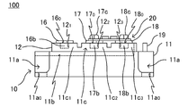
- the configuration of the semiconductor device is shown in top view.
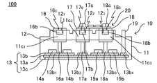
- the configuration of the semiconductor device is shown in a side view.
- 1 shows an internal configuration of a semiconductor device.
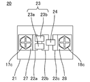
- the structure of a vibration suppression circuit is shown.
- the structure of the vibration suppression circuit which concerns on a modification is shown.
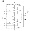
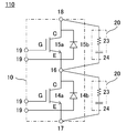
- 1 shows a circuit configuration of a semiconductor device.
- the circuit configuration of the semiconductor device concerning the 1st modification is shown. It shows transient changes of current and voltage at turn-on.
- the circuit structure of the semiconductor device which concerns on a 2nd modification is shown.
- the circuit structure of the semiconductor device which concerns on a 3rd modification is shown.
- the circuit structure of the semiconductor device which concerns on a 4th modification is shown.
- FIGS. 1A and 1B and FIG. 2 respectively show a configuration and an internal configuration in a top view and a side view of a semiconductor device 100 according to the present embodiment.
- the vertical direction in FIG. 1A and the front and back direction in FIG. 1B and FIG. 2 are the vertical direction
- the horizontal direction in FIGS. 1A and 1B and FIG. 2 is the horizontal direction
- the vertical direction is the height direction.
- the semiconductor device 100 incorporates a vibration suppression circuit to suppress high frequency noise that may be generated when the switch element is turned on, and preferably to configure a vibration suppression circuit having high reliability against stress such as thermal stress. Purpose.
- the semiconductor device 100 includes a housing 10, a substrate 13, semiconductor elements 14a and 15a, SiC diode elements 14b and 15b, external terminals 16 to 18, conductive members 16a to 18a, an external terminal 19, and a vibration suppression circuit 20.
- connection includes the meaning of being electrically connected in an electrically conductive manner, unless otherwise specified.
- the housing 10 has the constituent parts of the semiconductor device 100 inside, but the upper end of the external terminal 19 protrudes so that the lower surface of the substrate 13 is exposed flush with the bottom surface of the housing 10 and sealed.
- 18 is a member which exposes and fixes each upper surface of 18 on the upper surface of the housing
- the housing 10 includes a main body 11 and a terminal housing 12 which are formed by molding using, for example, a thermosetting resin such as an epoxy resin.
- the housing 10 is not limited to molding, and may be configured to seal the components of the semiconductor device 100 by filling the internal space with a gel filler such as silicone gel. Moreover, the lower surface of the substrate 13 is exposed from the bottom surface of the housing 10 to seal the components in the housing 10, but the substrate 13 is soldered on a plate-shaped base member made of a metal material such as copper. Or the like, and the frame may be fixed on the periphery of the base member with an adhesive or the like, and the frame may be sealed on the inside as the case 10 having the base member on the bottom surface. . As a result, the heat generated by the semiconductor element described later is exhausted to the member on which the semiconductor device 100 is mounted, that is, the heat sink, via the substrate 13 and the base member.
- a gel filler such as silicone gel.
- the main body 11 has a substantially rectangular parallelepiped whose longitudinal direction is a uniaxial direction (i.e., a lateral direction), and a substantially rectangular parallelepiped projecting portion 11c which protrudes upward from the center of the upper surface.
- a recess 11b extending from the center of the protrusion 11c to the left in the drawing in top view is formed.
- a terminal container 12 described later can be inserted into the recess 11 b.
- the main body 11 has a substantially square-shaped step portion 11a in top view to the four corners, the through hole 11a 0 penetrating in the height direction in each of the step portions 11a are formed.
- the projecting portion 11c together with the terminal accommodating body 12 inserted into the recess 11b, constitutes a plurality of terminal accommodating portions 11c 1 to 11c 3 connected in a uniaxial direction via the groove portion.
- the projecting portion 11c accommodates external terminals 16 to 18 described later at positions in the recess 11b corresponding to the three terminal accommodating portions 11c 1 to 11c3, respectively.
- ⁇ the external terminals 16 18 have a side view U-shape, toward their upper surface pores 16 0-18 0 is formed at the center on the upper one side of the longitudinal open end of the U-shaped
- the terminal accommodating body 12 is disposed in the recess 11 b so that the terminal accommodating body 12 can be inserted in the lateral direction.
- the terminal accommodating body 12 is a member that accommodates the terminals 16 b to 18 b and fixes the external terminals 16 to 18.
- the terminal accommodating body 12 has the same shape as the recess 11 b of the main body 11, that is, on a flat plate whose longitudinal direction is a longitudinal direction, corresponding to the three terminal accommodating portions 11 c 1 to 11 c 3 is connected via a groove in one axial direction.
- holes 12 1 to 12 3 having a hexagonal shape in top view are formed, and a nut having the same shape faces the female screw in the height direction as an example of the terminals 16b to 18b.
- Each is housed.
- a plurality of (three in this embodiment) terminal accommodating portions 11 c 1 to 11 c 3 pass the above-mentioned terminal accommodating body 12 through the inside of each of the external terminals 16 to 18 accommodated in the recess 11 b of the main body 11. , And the inside of the recess 11b is inserted to the right in the drawing.
- terminal (i.e., nuts) internal thread 16b ⁇ 18b are vertical and are positioned laterally, high and the hole 16 0-18 0 of the external terminals 16-18 It will communicate in the longitudinal direction.
- external terminals 16 to 18 are connected via conductive plates (not shown) for connecting bolts 17c and 18c, which are an example of a fixing tool, to additional substrate 21 of vibration suppression circuit 20 described later and other semiconductor devices and the like.
- the substrate 13 is a member on a flat plate on which a semiconductor element or the like is mounted.
- a DCB (Direct Copper Bonding) substrate, an AMB (Active Metal Brazing) substrate or the like can be adopted.
- the substrate 13 includes an insulating plate 13a and circuit layers 13b and 13c.
- the insulating plate 13a is a plate-like member made of, for example, an insulating ceramic such as aluminum nitride, silicon nitride, or aluminum oxide.
- the circuit layers 13 b and 13 c are provided on the upper surface and the lower surface of the insulating plate 13 a using conductive metals such as copper and aluminum, for example.
- the circuit layer 13 b includes wiring patterns 13 b 1 to 13 b 4 connected to the semiconductor element and / or the conductive member.
- the semiconductor elements 14a and 15a are an example of the first and second semiconductor elements (may be an example of the second and first semiconductor elements), and are switching elements formed of a compound semiconductor such as SiC, for example.
- a vertical metal oxide semiconductor field effect transistor (MOSFET), an insulated gate bipolar transistor (IGBT), or the like, each having an electrode may be employed.
- the semiconductor elements 14a and 15a are not limited to vertical elements, and may be horizontal elements provided with electrodes only on the surface.
- the semiconductor elements 14a and 15a, respectively, are mounted on the wiring pattern 13b 1 and 13b 3 on the substrate 13.
- the semiconductor elements 14a and 15a have an emitter electrode (source electrode) and a gate electrode on the surface, and a collector electrode (drain electrode) on the back surface.
- the semiconductor elements 14a and 15a, due bonding material such as solder, respectively, are fixed on the substrate 13 by bonding the back surface to the wiring pattern 13b 1 and 13b 3.
- the SiC diode elements 14b and 15b are respectively an example of the first and second SiC diode elements (may be an example of the second and first SiC diode elements) and are rectifying elements made of SiC, and as an example, each of the front and back surfaces A vertical Schottky barrier diode (SBD) having an electrode can be adopted.
- the SiC diode elements 14b and 15b are not limited to vertical elements, and may be horizontal elements having electrodes provided only on the surface.
- SiC diode element 14b and 15b, respectively, are mounted on the wiring pattern 13b 1 and 13b 3 on the substrate 13.
- the SiC diode elements 14 b and 15 b have an anode electrode on the front surface and a cathode electrode on the back surface.
- SiC diode element 14b and 15b, the joining material such as solder, respectively, are fixed on the substrate 13 by bonding the back surface to the wiring pattern 13b 1 and 13b 3.
- the cathode electrodes of SiC diode elements 14b and 15b are connected to the collector electrodes of semiconductor elements 14a and 15a, respectively.
- the anode electrodes of the SiC diode elements 14b and 15b are formed of, for example, a wire (not shown) made of a conductive metal such as copper or aluminum or a conductive alloy such as an iron aluminum alloy, respectively. It is connected to the emitter electrode. Thereby, SiC diode elements 14b and 15b are connected in anti-parallel to semiconductor elements 14a and 15a, respectively, to configure a switching device.
- the emitter electrode of the semiconductor element 15a using a wire (not shown), is connected to the wiring pattern 13b 1 on the substrate 13.
- the semiconductor element 15a and the SiC diode element 15b connected in antiparallel are connected in series to the semiconductor element 14a and the SiC diode element 14b connected in antiparallel.
- SiC anode electrode of the diode element 14b is connected to the wiring pattern 13b 2 on the further substrate 13 using a wire (not shown), gate electrodes of the semiconductor elements 14a and 15a are wire (not shown) the substrate 13 using It is connected to the wiring pattern 13b 4 above.
- the external terminals 16 to 18 are terminals for conducting current output from the semiconductor elements 14a and 15a and outputting the same to the outside of the semiconductor device 100.
- a side view of a plate member made of a conductive metal such as copper or aluminum It is formed in a U-shape.
- the conductive members 16a to 18a are provided between the wiring patterns 13b 1 to 13b 3 on the substrate 13 and the external terminals 16 to 18, respectively, and conduct currents output from the semiconductor elements 14a and 15a between them.
- the conductive member is formed in a flat plate shape or a cylindrical shape using a conductive metal such as copper or aluminum as an example.
- the conductive members 16a to 18a are erected on the substrate 13 by joining their lower ends to the wiring patterns 13b 1 to 13b 3 with a bonding material such as solder or by ultrasonic bonding, and solder or braze each upper end Or connected to the lower surfaces of the external terminals 16 to 18 by caulking.
- a bonding material such as solder or by ultrasonic bonding
- the emitter electrode of the semiconductor element 14a and the anode electrode of the SiC diode element 14b are connected to the external terminal 17 through the wiring pattern 13b 2 , a wire (not shown), and the terminal 17b by the conductive member 17a.
- the conductive member 18a the cathode electrode of the collector electrode and the SiC diode element 15b of the semiconductor element 15a is connected to the external terminals 18 through wiring patterns 13b 3 and the terminal 18b.
- the external terminal 19 is a terminal for inputting control signals to the semiconductor elements 14a and 15a from the outside of the semiconductor device 100 and outputting the output signals of the semiconductor elements 14a and 15a to the outside of the semiconductor device 100.
- the external terminal 19 is formed in a flat plate shape whose longitudinal direction is a longitudinal direction using a conductive metal such as copper or aluminum.
- the external terminal 19 includes four terminals, is erected on the wiring pattern 13 b 4 of the substrate 13, and protrudes from the top surface of the housing 10.
- the wiring patterns 13b 4 is connected to the gate electrode and the emitter electrode of the semiconductor elements 14a, 15a via a wire (not shown).
- Two terminals of the external terminal 19 is connected to the gate electrode of the semiconductor elements 14a and 15a through the wiring pattern 13b 4 and the wire (not shown), functions as a gate terminal.
- the remaining two terminals of the external terminal 19 is connected to the emitter electrode of the semiconductor element 14a and 15a through the wiring pattern 13b 4 and the wire (not shown), functions as an emitter terminal.
- FIG. 3A shows the configuration of the vibration suppression circuit 20 in a top view.
- the semiconductor device 100 on which a SiC element such as SiC-SBD is mounted high-speed noise may be generated particularly at turn-on because the operation is fast.
- the noise has a higher frequency of, for example, 10 MHz or more and 20 MHz or less due to the junction capacitance of the SiC-SBD, so there is a possibility that the parasitic capacitance in the device passes through with little attenuation and leaks out of the device.
- the vibration suppression circuit 20 generates the SiC diode element 15b in response to such high frequency noise, that is, voltage fluctuation generated in the SiC diode element 14b in response to turning on of the semiconductor element 15a and / or turning on of the semiconductor element 14a. It suppresses voltage fluctuations (for example, high frequency noise) that occur.
- the vibration suppression circuit 20 includes an additional substrate 21, a resistor 23, and a capacitor 24.
- the additional substrate 21 is a flat plate-like member for mounting the resistor 23 and the capacitor 24 and attaching the vibration suppression circuit 20 to the casing from the outside of the casing 10, for example, a DCB (Direct Copper Bonding) substrate, AMB Active Metal Blazing) substrates can be adopted, and a printed circuit can also be adopted.
- the additional substrate 21 is formed into a plate shape using an insulating ceramic such as aluminum nitride, silicon nitride, or aluminum oxide, for example, and has three wiring patterns spaced apart from each other on the surface thereof using a conductive metal such as copper or aluminum. 22a to 22c are provided.
- through holes (not shown) for passing bolts 17 c and 18 c which are an example of a fixing tool are formed on the left and right sides of the drawing, respectively.
- the resistor 23 is a resistive element for consuming the power of high frequency noise output from the semiconductor device 100.
- the resistor 23 is configured by connecting two resistor elements 23 a and 23 b in parallel, and both ends thereof are respectively connected to the wiring patterns 22 a and 22 b of the additional substrate 21.
- the resistor 23, that is, the resistor elements 23a and 23b, is formed into a shape that can be at least slightly deformed, for example, a U shape in a side view using a resistive material having elasticity, and both ends thereof are respectively connected to different wiring patterns It may be Here, when a large current transiently flows in the semiconductor device 100 to generate thermal stress, or a large current transiently flows in a conductive member or a conductive member connected to the device in the device to generate a magnetic field.
- the external terminals 16 to 18 to which the vibration suppression circuit 20 is connected may be stressed by the magnetic field.
- the mechanical resistance of the additional substrate 21 is flexibly deformed by the resilient resistor 23 to absorb the vibration, thereby, for example, maintaining good bonding of the resistive elements 23a and 23b to the additional substrate 21 to obtain a machine. It is possible to improve the reliability of the vibration suppression circuit 20 against the dynamic vibration.
- the capacitor 24 is a capacitive element for absorbing the power of high frequency noise output from the semiconductor device 100.
- the capacitor 24 is connected between the wiring patterns 22 b and 22 c of the additional substrate 21 and connected in series with the resistor 23.
- the capacitor 24 is formed so as to be at least slightly deformable using an elastic dielectric such as a film, paper or the like. Thereby, by flexibly deforming and absorbing the mechanical vibration of the additional substrate 21, for example, a good bonding of the capacitor 24 to the additional substrate 21 is maintained to suppress the vibration suppression circuit 20 for the mechanical vibration. Reliability can be improved.
- the capacitor 24 has a capacitance of, for example, 100 nF, more preferably, 1 nF or more and 20 nF or less.
- the resistor 23 has, for example, a resistance of 1 ⁇ to 10 ⁇ .
- the vibration suppression circuit 20 suppresses voltage fluctuation of 1 MHz or more and 100 MHz, preferably 10 MHz or more, and more preferably 10 MHz or more and 20 MHz or less.
- the vibration suppression circuit 20 includes a housing 10 that an upper surface of the external terminals 17 and 18 are exposed, that is, mounted on the upper surface of the terminal accommodating portion 11c 1 and 11c 2.
- the vibration suppression circuit 20 further includes through holes (not shown) provided on the additional substrate 21 via the rectangular washers 27 and 28 as the bolts 17 c and 18 c which are an example of the fixture.
- the wiring patterns 22a and 22c on the additional substrate 21 are connected to the external terminals 17 and 18 by the bolts 17c and 18c, respectively, and the resistor 23 and the capacitor 24 are connected in series between them.
- the vibration suppression circuit 20 may be mounted on the side surface of the projecting portion 11c of the case 10 constituting the terminal accommodating portions 11c 1 to 11c 3 or one side of the terminal accommodating body 12 in the longitudinal direction.
- the side surface of the protruding portion 11c or the terminal housing body 12, for example, a recess extending in the transverse direction is provided, the external terminal 16 is accommodated in the recess 11b so as to correspond to the terminal accommodating portion 11c 1 ⁇ 11c 3 on them -
- the vibration suppression circuit 20 may be configured by inserting a resistance element and a capacitance element connected in series between any two of the three wirings connected to 18 and any two of the three wirings.
- the vibration suppression circuit 20 having the above-described configuration and the bolts 17c and 18c for fixing the same to the housing 10
- the vibration suppression circuit 20 having an appropriate resistance and capacitance for the internal circuit of the semiconductor device 100 is selected.
- it can be detachably fixed to the terminal accommodating portions 11c 1 to 11c 3 of the housing 10 or to the side surfaces of the terminal accommodating portions 11c 1 to 11c 3 or the projecting portion 11c.
- FIG. 3B shows a configuration of a vibration suppression circuit 20 ′ according to a modification in top view.
- the vibration suppression circuit 20 ′ has an additional substrate 21 (21 a and 21 b), a resistor 23, and a capacitor 24.
- the same or corresponding members as those of the components of the vibration suppression circuit 20 described above are designated by the same reference numerals, and the description thereof will be omitted.
- the additional substrate 21 includes a first partial substrate 21a and a second partial substrate 21b separated from each other.
- the first partial substrate 21 a can be configured in the same manner as the additional substrate 21 of the vibration suppression circuit 20.
- one wiring pattern 22a is provided on the surface.
- bolt 17c which is an example of a fixing tool pass is formed.
- the second partial substrate 21 a can be configured in the same manner as the additional substrate 21 of the vibration suppression circuit 20.
- two wiring patterns 22b and 22c spaced apart from each other are provided on the surface.
- bolt 18c which is an example of a fixing tool pass is formed.
- the resistor 23 is configured by combining two resistor elements 23a and 23b in parallel, and both ends thereof are respectively connected to the wiring pattern 22a of the first partial substrate 21a and the wiring pattern 22b of the second partial substrate 21b.
- Ru the resistor 23, that is, the resistor elements 23a and 23b, is formed into a shape that can be at least slightly deformed, for example, a U shape in a side view using a resistive material having elasticity, and the first partial substrate 21a and the second partial substrate 21b.
- the mechanical deformation of the additional substrate 21, ie, the first partial substrate 21 a and the second partial substrate 21 b, is flexibly deformed to absorb the vibration, for example, resistance elements 23 a and 23 b to the additional substrate 21. Good bonding can be maintained to improve the reliability of the vibration suppression circuit 20 'against mechanical vibrations.
- the capacitor 24 is connected between the wiring patterns 22 b and 22 c of the second partial substrate 21 b and connected in series with the resistor 23.
- the capacitor 24 is formed so as to be at least slightly deformable using an elastic dielectric such as a film, paper or the like. Thereby, by flexibly deforming and absorbing the mechanical vibration of the additional substrate 21, for example, a good bonding of the capacitor 24 to the additional substrate 21 is maintained to suppress the vibration suppression circuit 20 for the mechanical vibration. The 'reliability can be improved.
- the capacitor 24 may be provided across them.
- the first partial substrate 21 a is not limited to separating the first partial substrate 21 a and the second partial substrate 21 b from each other, for example, slits may be provided between them to partially separate and partially separate the first partial substrate 21 a
- a resistor 23 and / or a capacitor 24 may be provided across the second partial substrate 21 b.
- FIG. 4A shows a circuit configuration of the semiconductor device 100.
- the semiconductor elements 14a and 15a are connected in series between the external terminals 17 and 18 via the wiring patterns 13b 1 to 13b 3 , wires (not shown), and conductive members 17a and 18a.
- SiC diode element 14b is connected in parallel to the semiconductor device 14a through the wiring pattern 13b 1 and the wire (not shown)
- the SiC diode element 15b is a semiconductor device 15a through the wiring pattern 13b 3 and the wires (not shown) Connected in parallel.
- the vibration suppression circuit 20 is connected between the external terminals 17 and 18 in parallel with the semiconductor elements 14 a and 15 a (and the SiC diode elements 14 b and 15 b).
- a control signal (a switching signal included therein) is input to each of the gate electrodes via the external terminal 19, the wiring pattern 13b 4 , and a wire (not shown).
- the current is switched from the external terminal 18 to the external terminal 16 or from the external terminal 16 to the external terminal 17 or stopped.
- the vibration suppression circuit 20 causes a voltage fluctuation generated in the SiC diode element 14b in response to the semiconductor element 15a being turned on and / or a voltage fluctuation generated in the SiC diode element 15b in response to the semiconductor element 14a being turned on (for example, Suppress high frequency noise).
- the vibration suppression circuit 20 is not limited to being provided commonly to the semiconductor elements 14a and 15a (and the SiC diode elements 14b and 15b), but the semiconductor element 14a (and the SiC diode element 14b) and the semiconductor element 15a (and the SiC diode) You may provide separately with respect to each of element 15 b).
- FIG. 4B shows a circuit configuration of the semiconductor device 110 according to the first modification.
- the semiconductor elements 14 a and 15 a and the SiC diode elements 14 b and 15 b are connected between the external terminals 17 and 18 in the same manner as the semiconductor device 100.
- one of the two vibration suppression circuits 20 is connected in parallel with the semiconductor element 14 a (and the SiC diode element 14 b) between the external terminals 16 and 17, and the other is the semiconductor between the external terminals 16 and 18. It is connected in parallel with the element 15a (and the SiC diode element 15b).
- the vibration suppression circuit 20 connected between the external terminals 16 and 17 suppresses voltage fluctuation generated in the SiC diode element 14b in response to the semiconductor element 15a being turned on.
- the vibration suppression circuit 20 connected between the two suppresses the voltage fluctuation generated in the SiC diode element 15b in response to the turning on of the semiconductor element 14a.
- the vibration suppression circuit 20 is not limited to each of the semiconductor element 14a (and the SiC diode element 14b) and the semiconductor element 15a (and the SiC diode element 15b). It may be provided.
- FIG. 5 shows the results of the transient response test of current and voltage at turn-on of the semiconductor device in the semiconductor devices 100 and 110.
- the vibration suppression circuit 20 of the semiconductor device 100 the resistance 2.5 ⁇ of the resistor 23 and the capacitance 11 nF of the capacitor 24 are used. This is referred to as Example 1.
- the vibration suppression circuit 20 of the semiconductor device 110 the resistance of the resistor 23 is 6.8 ⁇ and the capacitance of the capacitor 24 is 5.2 nF.
- Example 2 a semiconductor device 100 not including the vibration suppression circuit 20 is taken as a comparative example.
- the current I C gradually increases and peaks at approximately 280 ns and starts to decrease, and dips at approximately 330 ns and starts to increase again at approximately 370 ns. A peak appears again, and then it begins to decrease, and thereafter it repeats saturation (i.e., vibration) at a period of 80 ns or more and 100 ns or less to saturate.
- the voltage V CE sharply increases from about 280 ns, peaks at about 320 ns and starts to decrease, dips at about 370 ns and starts to increase again, and peaks again at 430 ns.
- the increase and decrease (that is, the vibration at 10 MHz or more and 12.5 MHz or less) is repeated and saturated in a cycle of 80 ns or more and 100 ns or less.
- the oscillations of the current I C and the voltage V CE attenuate in about 1200 ns.
- the current I C when the semiconductor element 14a is turned on, gradually increases and peaks at approximately 280 ns and starts to decrease, and dips at approximately 330 ns and starts to increase again to approximately 350 ns. Almost constant.
- the voltage V CE sharply increases from about 280 ns and peaks at about 320 ns and starts to decrease, dips at about 380 ns and increases again, and then gradually increases and saturates .
- the oscillation of the current I C and the voltage V CE is smaller than that of the comparative example 1, and attenuates in about 100 ns.
- the current I C when the semiconductor element 14a is turned on, gradually increases and peaks at approximately 260 ns and starts to decrease, and dips at approximately 315 ns and starts to increase again to approximately 350 ns. The peak again appears, and then it begins to decrease, and thereafter it is saturated by repeating minute increase / decrease (that is, minute vibration) in a short cycle of about 50 ns.
- the voltage V CE rapidly increases from about 280 ns, peaks at about 310 ns and turns to decrease, dips at about 370 ns and turns to increase again, and thereafter it is minute with a short period of about 50 ns. Repeatedly increase and decrease (ie, minute vibration) to saturate.
- the oscillations of the current I C and the voltage V CE are smaller than those of Comparative Example 1, but are larger than that of Example 1, and attenuate in about 300 ns.
- the vibration suppression circuit 20 in both the semiconductor devices 100 and 110 enables high-frequency current and voltage at turn-on of the semiconductor element. It has been confirmed that the fluctuation can be suppressed. That is, the vibration suppression circuit 20 can suppress high frequency (for example, 10 MHz or more and 20 MHz or less) noise as compared with the conventional RC snubber.
- an RC snubber circuit may be connected in parallel to the vibration suppression circuit 20.
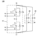
- FIG. 6A shows a circuit configuration of a semiconductor device 120 according to a second modification. Similar to semiconductor device 100, semiconductor elements 14a and 15a and SiC diode elements 14b and 15b are connected between external terminals 17 and 18, and vibration suppression circuit 20 is connected between external terminals 17 and 18 in parallel thereto. ing. On the other hand, an RC snubber circuit 30 is further connected in parallel with the vibration suppression circuit 20.
- the RC snubber circuit 30 has a resistor 33 and a capacitor 34 connected in series.
- the capacitor 34 has a capacitance of, for example, 400 nF to 10 ⁇ F.
- the resistor 33 has a resistance of, for example, 100 ⁇ or more.
- the RC snubber circuit 30 absorbs the surge voltage (Ldi / dt) generated in the wiring inductance (L) in the device due to a rapid current change (di / dt) when the semiconductor element 14a or 15a is turned off.
- the vibration suppression circuit 20 described above has a low ability to absorb this surge voltage.
- a C collective snubber circuit having only a capacitor may be used.
- FIG. 6B shows a circuit configuration of a semiconductor device 130 according to a third modification. Similar to semiconductor device 100, semiconductor elements 14a and 15a and SiC diode elements 14b and 15b are connected between external terminals 17 and 18, and vibration suppression circuit 20 is connected between external terminals 17 and 18 in parallel thereto. ing. On the other hand, a C batch snubber circuit 40 is further connected in parallel with the vibration suppression circuit 20.
- the C collective snubber circuit 40 has a capacitor 44.
- the capacitor 44 has a capacitance of, for example, 400 nF or more and 10 ⁇ F or less.
- the RC snubber circuit 30 it is possible to absorb the surge voltage applied to the semiconductor element 14a or 15a when the semiconductor element 14a or 15a is turned off.
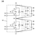
- FIG. 6C shows a circuit configuration of a semiconductor device 140 according to the fourth modification. Similar to the semiconductor device 110, the semiconductor elements 14a and 15a and the SiC diode elements 14b and 15b are connected between the external terminals 17 and 18, and one of the two vibration suppression circuits 20 is a semiconductor between the external terminals 16 and 17. The other is connected between the external terminals 16 and 18 in parallel with the semiconductor element 15a (and the SiC diode element 15b). On the other hand, one of two RC snubber circuits 30 is connected between external terminals 16 and 17 in parallel with one vibration suppression circuit 20, and two RC snubber circuits are connected in parallel with the other vibration suppression circuit 20. The other 30 is connected between the external terminals 16 and 18.
- the two RC snubber circuits 30 are configured in the same manner as the RC snubber circuit 30 in the semiconductor device 120.
- the RC snubber circuit 30 connected between the external terminals 16 and 17 absorbs a surge voltage applied to the semiconductor element 14a when the semiconductor element 14a is turned off.
- the RC snubber circuit 30 connected between the external terminals 16 and 18 absorbs a surge voltage applied to the semiconductor element 15a when the semiconductor element 15a is turned off.
- the C collective snubber circuit 40 may be used instead of at least one of the two RC snubber circuits 30.
- the vibration suppression circuit 20 is fixed on the housing 10 (that is, the terminal accommodating portions 11c 1 to 11c 3 ), but instead, the semiconductor element 14a and the semiconductor element 14a 15a may be incorporated on the substrate 13 mounted.
- the semiconductor device 100 according to the present embodiment and the semiconductor devices 110 to 140 according to the modification include the two semiconductor elements 14a and 15a, for example, a plurality of semiconductor elements 14a may be externally connected in series and / or in parallel. It may be connected between the terminals 16 and 17, or a plurality of semiconductor elements 15a may be connected in series and / or in parallel between the external terminals 16 and 18. Similarly, a plurality of SiC diode elements 14b may be connected in series and / or in parallel between external terminals 16 and 17, or a plurality of SiC diode elements 15b may be connected in series and / or in parallel between external terminals 16 and 18. May be
- 10 housing, 11 ... main body, 11a ... stepped portion, 11A0 ... through hole, 11b ... recess, 11c ... projecting portion, 11c 1 ⁇ 11c 3 ... terminal accommodating portion, 12 ... terminal accommodating body 12 1-12 3 ...
Landscapes
- Engineering & Computer Science (AREA)
- Power Engineering (AREA)
- Power Conversion In General (AREA)
- Inverter Devices (AREA)
- Electronic Switches (AREA)
Abstract
SiC素子を搭載した半導体装置において発生する高周波のノイズを抑制する。半導体装置100は、直列に接続された半導体素子14a及び15a、半導体素子14aに並列に接続されるSiCダイオード素子14b、半導体素子14a及びSiCダイオード素子14bと並列に接続され、半導体素子15aがターンオンしたことに応じてSiCダイオード素子14bに生じる電圧変動を抑制する振動抑制回路20を備える。振動抑制回路20により、半導体素子15aがターンオンしたことに応じてSiCダイオード素子14bに生じる電圧変動が抑制され、半導体装置100に対する信頼性が向上する。
Description
本発明は、半導体装置及び振動抑制装置に関する。
半導体装置の一例として、絶縁ゲートバイポーラトランジスタ(IGBT)、金属酸化物半導体電界効果トランジスタ(MOSFET)等のスイッチ素子にショットキーバリアダイオード(SBD)等の整流素子を逆並列に接続して構成されるスイッチ装置又はこれを2つ直列に接続して構成される装置が、パワーコンディショナ(PCS)、インバータ、スマートグリッド等の電力変換システムに組み込まれる。これらのシステムにおいて、半導体装置内のスイッチ素子がターンオン若しくはターンオフする際又は整流素子における逆回復時に、急激な電流変化(di/dt)により装置内の配線インダクタンス(L)にサージ電圧(Ldi/dt)が発生し、これに起因して例えば10kHz以下の高周波のノイズがシステム内の他の装置に漏洩することがある。
そこで、例えば特許文献1には、半導体装置内の主回路に電気的に接続し且つ外部に露出する2つの端子の間にスナバ回路が接続された半導体装置が開示されている。スナバ回路として、抵抗素子及びコンデンサ素子を直列に接続して構成されるRCスナバが採用されている。RCスナバにより、サージ電圧に起因する高周波のノイズが吸収されて、装置外への漏洩を防止することができる。
特許文献1 特開2014-128066号公報
特許文献1 特開2014-128066号公報
近年、シリコンカーバイド化合物半導体(SiC)素子等の化合物半導体素子のような次世代半導体素子を搭載したパワー半導体装置(単に、半導体装置と呼ぶ)の開発が進められている。SiC素子は、従来のシリコン半導体(Si)素子に対して絶縁破壊電界強度が高いことから高耐圧であり、また不純物濃度をより高く、活性層をより薄くすることができることから高効率且つ高速動作が可能な小型の半導体装置を実現することができる。しかし、この様な半導体素子は高速動作が可能であることから、従来のRCスナバ或いはCスナバでは解決できない(又は抑制できない)高周波のノイズが発生し得る。
(項目1)
半導体装置は、直列に接続された第1半導体素子および第2半導体素子を備えてよい。
半導体装置は、第1半導体素子に並列に接続される第1SiCダイオード素子を備えてよい。
半導体装置は、第1半導体素子および第1SiCダイオード素子と並列に接続され、第2半導体素子がターンオンしたことに応じて第1SiCダイオード素子に生じる電圧変動を抑制する第1振動抑制回路を備えてよい。
(項目2)
半導体装置は、第2半導体素子に並列に接続される第2SiCダイオード素子を更に備えてよい。
(項目3)
第1振動抑制回路は、直列に接続した抵抗およびキャパシタを有してよい。
(項目4)
第1振動抑制回路は、10MHz以上の電圧変動を抑制してよい。
(項目5)
第1振動抑制回路は、1MHz以上100MHz以下の電圧変動を抑制してよい。
(項目6)
キャパシタは、100nF以下の容量を有してよい。
(項目7)
キャパシタは、1nF以上20nF以下の容量を有してよい。
(項目8)
第1振動抑制回路が有する抵抗およびキャパシタの少なくとも一方は、弾性を有してよい。
(項目9)
半導体装置は、第1半導体素子、第2半導体素子、第1SiCダイオード素子、および第2SiCダイオード素子を収容する筐体を更に備えてよい。
筐体は、第1半導体素子における第2半導体素子とは反対側に接続され、第1の外部端子と接続されるべき第1端子を収容する、筐体の本体部分から突出した第1端子収容部と、第1半導体素子および第2半導体素子の間、または第2半導体素子における第1半導体素子とは反対側に接続され、第2の外部端子と接続されるべき第2端子を収容する、筐体の本体部分から突出した第2端子収容部と、を有してよい。
(項目10)
第1振動抑制回路は、第1端子収容部および第2端子収容部における、第1の外部端子および第2の外部端子が接続される面に搭載されてよい。
(項目11)
第1振動抑制回路は、第1端子収容部内の第1端子に対して第1の外部端子と共にネジ止めされると共に、第2端子収容部内の第2端子に対して第2の外部端子と共にネジ止めされてよい。
(項目12)
第1振動抑制回路は、第1端子収容部および第2端子収容部における、第1の外部端子および第2の外部端子が接続される面に対して側方に位置する側面に搭載されてよい。
(項目13)
第1振動抑制回路は、筐体の外側から筐体に取り付けられる付加基板を有してよい。
付加基板が第1端子収容部および第2端子収容部に対して固定されてよい。
(項目14)
付加基板は、分離した第1部分基板および第2部分基板を含んでよい。
第1振動抑制回路は、直列に接続した抵抗およびキャパシタを有し、抵抗およびキャパシタの少なくとも一方は弾性を有し、第1部分基板および第2部分基板間を跨いで設けられてよい。
(項目15)
第1振動抑制回路は、第1半導体素子における第2半導体素子とは反対側に接続される第1端子と第1半導体素子および第2半導体素子の間に接続される第2端子との間に接続されてよい。
(項目16)
半導体装置は、第2半導体素子における第2端子側とは反対側に接続される第3端子と第2端子との間に設けられ、第1半導体素子がターンオンしたことに応じて第2SiCダイオード素子に生じる電圧変動を抑制する第2振動抑制回路を更に備えてよい。
(項目17)
第1振動抑制回路は、第1半導体素子における第2半導体素子とは反対側に接続される第1端子と、第2半導体素子における第1半導体素子とは反対側に接続される第2端子との間に設けられてよい。
(項目18)
半導体装置は、第1半導体素子、第1SiCダイオード素子、および第1振動抑制回路と並列に接続されたRCスナバ回路を更に備えてよい。
(項目19)
RCスナバ回路は、400nF以上10μF以下の容量を有するキャパシタを有してよい。
半導体装置は、直列に接続された第1半導体素子および第2半導体素子を備えてよい。
半導体装置は、第1半導体素子に並列に接続される第1SiCダイオード素子を備えてよい。
半導体装置は、第1半導体素子および第1SiCダイオード素子と並列に接続され、第2半導体素子がターンオンしたことに応じて第1SiCダイオード素子に生じる電圧変動を抑制する第1振動抑制回路を備えてよい。
(項目2)
半導体装置は、第2半導体素子に並列に接続される第2SiCダイオード素子を更に備えてよい。
(項目3)
第1振動抑制回路は、直列に接続した抵抗およびキャパシタを有してよい。
(項目4)
第1振動抑制回路は、10MHz以上の電圧変動を抑制してよい。
(項目5)
第1振動抑制回路は、1MHz以上100MHz以下の電圧変動を抑制してよい。
(項目6)
キャパシタは、100nF以下の容量を有してよい。
(項目7)
キャパシタは、1nF以上20nF以下の容量を有してよい。
(項目8)
第1振動抑制回路が有する抵抗およびキャパシタの少なくとも一方は、弾性を有してよい。
(項目9)
半導体装置は、第1半導体素子、第2半導体素子、第1SiCダイオード素子、および第2SiCダイオード素子を収容する筐体を更に備えてよい。
筐体は、第1半導体素子における第2半導体素子とは反対側に接続され、第1の外部端子と接続されるべき第1端子を収容する、筐体の本体部分から突出した第1端子収容部と、第1半導体素子および第2半導体素子の間、または第2半導体素子における第1半導体素子とは反対側に接続され、第2の外部端子と接続されるべき第2端子を収容する、筐体の本体部分から突出した第2端子収容部と、を有してよい。
(項目10)
第1振動抑制回路は、第1端子収容部および第2端子収容部における、第1の外部端子および第2の外部端子が接続される面に搭載されてよい。
(項目11)
第1振動抑制回路は、第1端子収容部内の第1端子に対して第1の外部端子と共にネジ止めされると共に、第2端子収容部内の第2端子に対して第2の外部端子と共にネジ止めされてよい。
(項目12)
第1振動抑制回路は、第1端子収容部および第2端子収容部における、第1の外部端子および第2の外部端子が接続される面に対して側方に位置する側面に搭載されてよい。
(項目13)
第1振動抑制回路は、筐体の外側から筐体に取り付けられる付加基板を有してよい。
付加基板が第1端子収容部および第2端子収容部に対して固定されてよい。
(項目14)
付加基板は、分離した第1部分基板および第2部分基板を含んでよい。
第1振動抑制回路は、直列に接続した抵抗およびキャパシタを有し、抵抗およびキャパシタの少なくとも一方は弾性を有し、第1部分基板および第2部分基板間を跨いで設けられてよい。
(項目15)
第1振動抑制回路は、第1半導体素子における第2半導体素子とは反対側に接続される第1端子と第1半導体素子および第2半導体素子の間に接続される第2端子との間に接続されてよい。
(項目16)
半導体装置は、第2半導体素子における第2端子側とは反対側に接続される第3端子と第2端子との間に設けられ、第1半導体素子がターンオンしたことに応じて第2SiCダイオード素子に生じる電圧変動を抑制する第2振動抑制回路を更に備えてよい。
(項目17)
第1振動抑制回路は、第1半導体素子における第2半導体素子とは反対側に接続される第1端子と、第2半導体素子における第1半導体素子とは反対側に接続される第2端子との間に設けられてよい。
(項目18)
半導体装置は、第1半導体素子、第1SiCダイオード素子、および第1振動抑制回路と並列に接続されたRCスナバ回路を更に備えてよい。
(項目19)
RCスナバ回路は、400nF以上10μF以下の容量を有するキャパシタを有してよい。
(項目20)
直列に接続された第1半導体素子および第2半導体素子と、第1半導体素子に並列に接続される第1SiCダイオード素子とを有する半導体装置に付加される振動抑制装置は、半導体装置の筐体に対して取り付けられて第1半導体素子および第1SiCダイオード素子と並列に接続され、第2半導体素子がターンオンしたことに応じて第1SiCダイオード素子に生じる電圧変動を抑制してよい。
(項目21)
振動抑制回路は、第1半導体素子および第1SiCダイオード素子と並列に接続される、直列に接続した抵抗およびキャパシタを有してよい。
(項目22)
筐体は、第1半導体素子における第2半導体素子とは反対側に設けられ、第1の外部端子と接続されるべき第1端子を収容する、筐体の本体部分から突出した第1端子収容部と、第1半導体素子および第2半導体素子の間、または第2半導体素子における第1半導体素子とは反対側に設けられ、第2の外部端子と接続されるべき第2端子を収容する、筐体の本体部分から突出した第2端子収容部と、を有してよい。
当該振動抑制装置は、第1端子収容部および第2端子収容部における、第1の外部端子および第2の外部端子が接続される面、または、第1端子収容部および第2端子収容部における、第1の外部端子および第2の外部端子が接続される面に対して側方に位置する側面に搭載されてよい。
直列に接続された第1半導体素子および第2半導体素子と、第1半導体素子に並列に接続される第1SiCダイオード素子とを有する半導体装置に付加される振動抑制装置は、半導体装置の筐体に対して取り付けられて第1半導体素子および第1SiCダイオード素子と並列に接続され、第2半導体素子がターンオンしたことに応じて第1SiCダイオード素子に生じる電圧変動を抑制してよい。
(項目21)
振動抑制回路は、第1半導体素子および第1SiCダイオード素子と並列に接続される、直列に接続した抵抗およびキャパシタを有してよい。
(項目22)
筐体は、第1半導体素子における第2半導体素子とは反対側に設けられ、第1の外部端子と接続されるべき第1端子を収容する、筐体の本体部分から突出した第1端子収容部と、第1半導体素子および第2半導体素子の間、または第2半導体素子における第1半導体素子とは反対側に設けられ、第2の外部端子と接続されるべき第2端子を収容する、筐体の本体部分から突出した第2端子収容部と、を有してよい。
当該振動抑制装置は、第1端子収容部および第2端子収容部における、第1の外部端子および第2の外部端子が接続される面、または、第1端子収容部および第2端子収容部における、第1の外部端子および第2の外部端子が接続される面に対して側方に位置する側面に搭載されてよい。
なお、上記の発明の概要は、本発明の特徴の全てを列挙したものではない。また、これらの特徴群のサブコンビネーションもまた、発明となりうる。
以下、発明の実施の形態を通じて本発明を説明するが、以下の実施形態は請求の範囲にかかる発明を限定するものではない。また、実施形態の中で説明されている特徴の組み合わせの全てが発明の解決手段に必須であるとは限らない。
図1A及び図1B並びに図2は、それぞれ、本実施形態に係る半導体装置100の上面視及び側面視における構成並びに内部構成を示す。ここで、図1Aにおける上下方向及び図1B並びに図2における前奥方向を縦方向、図1A及び図1B並びに図2における左右方向を横方向、図1Aにおける前奥方向及び図1B並びに図2における上下方向を高さ方向とする。半導体装置100は、振動抑制回路を組み込むことによりスイッチ素子のターンオン時に発生し得る高周波ノイズを抑制すること、好ましくはさらに熱ストレス等のストレスに対して高い信頼性を有する振動抑制回路を構成することを目的とするものである。
半導体装置100は、筐体10、基板13、半導体素子14a及び15a、SiCダイオード素子14b及び15b、外部端子16~18、導電部材16a~18a、外部端子19、並びに振動抑制回路20を備える。
なお、本明細書において、「接続」とは、特に断らない限り、通電可能に電気的に接続する意味を含むものとする。
筐体10は、半導体装置100の構成各部を内部に、ただし外部端子19の上端を突出し、基板13の下面を筐体10の底面と面一に露出して封止するとともに、外部端子16~18のそれぞれの上面を筐体10の上面上に露出して固定する部材である。筐体10は、例えばエポキシ樹脂のような熱硬化性樹脂を用いてモールド成形することで形成される本体11及び端子収容体12を含む。
なお、筐体10は、モールド成形に限らず、内部空間にシリコーンゲル等のゲル充填材を充填することで半導体装置100の構成各部を封止してもよい。また、基板13の下面を筐体10の底面から露出して構成各部を筐体10内に封止するに限らず、基板13を例えば銅等の金属材料からなる板状のベース部材上にはんだ等の接合材により接合し、ベース部材の周縁上に枠体を接着剤等により固定し、これを底面にベース部材を有する筐体10として、その内部に構成各部を封止することとしてもよい。それにより、後述する半導体素子により発生した熱は、基板13及びベース部材を介して半導体装置100が実装される部材、すなわちヒートシンクに排熱される。
本体11は、一軸方向(すなわち、横方向)を長手とする略直方体及びこの上面中央から上方に突出する略直方体状の突出部11cを有する。本体11の上面には、上面視において突出部11cの中央から図面左方に延びる凹部11bが形成されている。凹部11b内に、後述する端子収容体12を挿入することができる。また、本体11は、4つの角部に上面視において略正方形状の段部11aを有し、それぞれの段部11aに高さ方向に貫通する貫通孔11a0が形成されている。貫通孔11a0に上方からボルト等の固定具を差し入れることで、半導体装置100を外部装置等に固定することができる。
突出部11cは、凹部11b内に挿入される端子収容体12とともに、一軸方向に溝部を介して連接する複数の端子収容部11c1~11c3を構成する。突出部11cは、3つの端子収容部11c1~11c3に対応する凹部11b内の位置にそれぞれ後述する外部端子16~18を収容する。ただし、外部端子16~18は、側面視U字状を有し、中央に孔部160~180が形成されたそれらの上面を上方に向け、U字の開口端を縦方向の一側に向け、これらの内側に端子収容体12を横方向に挿通可能に凹部11b内に配置される。
端子収容体12は、端子16b~18bを収容するとともに外部端子16~18を固定する部材である。端子収容体12は、本体11の凹部11bと同形状を有する、すなわち一軸方向を長手とする平板上に、3つの端子収容部11c1~11c3に対応して一軸方向に溝部を介して連接する3つの凸部を有する。3つの凸部のそれぞれの上面中央には、例えば上面視六角形状の穴部121~123が形成され、端子16b~18bの一例として同形状のナットが雌ネジを高さ方向に向けてそれぞれ収容されている。
複数(本実施形態では一例として3つ)の端子収容部11c1~11c3は、上述の端子収容体12を、本体11の凹部11b内に収容された外部端子16~18のそれぞれの内側を通して、凹部11b内を図面右方に挿入することで構成される。このとき、端子収容体12に収容された端子(すなわち、ナット)16b~18bの雌ネジが、縦方向及び横方向に位置決めされて、外部端子16~18の孔部160~180と高さ方向に連通することとなる。それにより、固定具の一例であるボルト17c及び18cを、後述する振動抑制回路20の付加基板21及び他の半導体装置等に接続するための導電板(不図示)を介し、外部端子16~18の孔部160~180を通して端子16b~18bの雌ネジに螺入することで、付加基板21及び導電板を外部端子16~18に着脱可能に接続するとともに筐体10に取外し可能に固定することができる。
基板13は、半導体素子等が搭載される平板上の部材であり、例えばDCB(Direct Copper Bonding)基板、AMB(Active Metal Brazing)基板等を採用することができる。基板13は、絶縁板13a並びに回路層13b及び13cを含む。絶縁板13aは、例えば窒化アルミニウム、窒化珪素、酸化アルミニウム等の絶縁性セラミックスから構成される板状部材である。回路層13b及び13cは、例えば銅、アルミニウム等の導電性金属を用いて、それぞれ絶縁板13aの上面及び下面に設けられている。なお、回路層13bは、半導体素子及び/又は導電部材に接続する配線パターン13b1~13b4を含む。
半導体素子14a及び15aは、それぞれ第1及び第2半導体素子の一例であり(第2及び第1半導体素子の一例でもよい)、例えばSiC等の化合物半導体からなるスイッチング素子であり、表面及び裏面のそれぞれに電極を有する縦型の金属酸化物半導体電界効果トランジスタ(MOSFET)、絶縁ゲートバイポーラトランジスタ(IGBT)等を採用することができる。なお、半導体素子14a及び15aは、縦型の素子に限らず、表面にのみ電極が設けられた横型の素子であってもよい。半導体素子14a及び15aは、それぞれ、基板13上の配線パターン13b1及び13b3上に搭載される。
半導体素子14a及び15aは、IGBT(又はMOSFET)の場合に、表面にエミッタ電極(ソース電極)及びゲート電極、裏面にコレクタ電極(ドレイン電極)を有する。半導体素子14a及び15aは、はんだ等の接合材により、それぞれ、裏面を配線パターン13b1及び13b3に接合することで基板13上に固定される。
SiCダイオード素子14b及び15bは、それぞれ第1及び第2SiCダイオード素子の一例であり(第2及び第1SiCダイオード素子の一例でもよい)、SiCからなる整流素子であり、一例として、表面及び裏面のそれぞれに電極を有する縦型のショットキーバリアダイオード(SBD)を採用することができる。なお、SiCダイオード素子14b及び15bは、縦型の素子に限らず、表面にのみ電極が設けられた横型の素子であってもよい。SiCダイオード素子14b及び15bは、それぞれ、基板13上の配線パターン13b1及び13b3上に搭載される。
SiCダイオード素子14b及び15bは、表面にアノード電極及び裏面にカソード電極を有する。SiCダイオード素子14b及び15bは、はんだ等の接合材により、それぞれ、裏面を配線パターン13b1及び13b3に接合することで基板13上に固定される。それにより、SiCダイオード素子14b及び15bのカソード電極は、それぞれ、半導体素子14a及び15aのコレクタ電極に接続される。
また、SiCダイオード素子14b及び15bのアノード電極は、例えば銅、アルミニウム等の導電性金属又は鉄アルミ合金等の導電性合金からなるワイヤ(不図示)を用いて、それぞれ、半導体素子14a及び15aのエミッタ電極に接続される。それにより、SiCダイオード素子14b及び15bは、それぞれ、半導体素子14a及び15aに逆並列に接続されてスイッチング装置を構成する。また、半導体素子15aのエミッタ電極は、ワイヤ(不図示)を用いて、基板13上の配線パターン13b1に接続される。それにより、逆並列に接続された半導体素子15a及びSiCダイオード素子15bが逆並列に接続された半導体素子14a及びSiCダイオード素子14bに直列に接続される。さらに、SiCダイオード素子14bのアノード電極はワイヤ(不図示)を用いてさらに基板13上の配線パターン13b2に接続され、半導体素子14a及び15aのゲート電極はワイヤ(不図示)を用いて基板13上の配線パターン13b4に接続される。
外部端子16~18は、半導体素子14a及び15aから出力される電流を導通して半導体装置100外に出力するための端子であり、例えば銅、アルミニウム等の導電性金属の板状部材を側面視U字状に変形して形成される。外部端子16~18は、先述のとおり、上面の中央にそれぞれ孔部160~180が形成され、3つの端子収容部11c1~11c3に対応する筐体10の凹部11b内の位置に配置される。
導電部材16a~18aは、それぞれ、基板13上の配線パターン13b1~13b3と外部端子16~18との間に設けられて、それらの間で半導体素子14a及び15aから出力される電流を通電するための導電性の部材であり、一例として銅、アルミニウム等の導電性金属を用いて平板状又は円柱状に成形されている。
導電部材16a~18aは、それぞれの下端をはんだ等の接合材により又は超音波接合により配線パターン13b1~13b3に接合することで基板13上に立設され、それぞれの上端をはんだ、ロウ付け、又はカシメにより外部端子16~18の下面に接続される。導電部材16aにより、半導体素子14aのコレクタ電極、SiCダイオード素子14bのカソード電極、半導体素子15aのエミッタ電極、及びSiCダイオード素子15bのアノード電極が配線パターン13b1、ワイヤ(不図示)、及び端子16b介して外部端子16に接続され、導電部材17aにより、半導体素子14aのエミッタ電極及びSiCダイオード素子14bのアノード電極が配線パターン13b2、ワイヤ(不図示)、及び端子17b介して外部端子17に接続され、導電部材18aにより、半導体素子15aのコレクタ電極及びSiCダイオード素子15bのカソード電極が配線パターン13b3及び端子18b介して外部端子18に接続される。
外部端子19は、半導体装置100外から半導体素子14a及び15aに制御信号を入力する、また半導体素子14a及び15aの出力信号を半導体装置100外に出力するための端子である。外部端子19は、例えば銅、アルミニウム等の導電性金属を用いて高さ方向を長手とする平板状に成形されている。外部端子19は、4つの端子を含み、基板13の配線パターン13b4上に立設され、筐体10の上面から突出する。なお、配線パターン13b4は、ワイヤ(不図示)を介して半導体素子14a及び15aのゲート電極及びエミッタ電極に接続されている。外部端子19のうちの2つの端子は、配線パターン13b4及びワイヤ(不図示)を介して半導体素子14a及び15aのゲート電極に接続されて、ゲート端子として機能する。また、外部端子19のうちの残りの2つの端子は、配線パターン13b4及びワイヤ(不図示)を介して半導体素子14a及び15aのエミッタ電極に接続されて、エミッタ端子として機能する。
図3Aは、振動抑制回路20の構成を上面視において示す。SiC-SBD等のSiC素子を搭載した半導体装置100では、その動作が高速であることから、特にターンオン時に高周波のノイズが発生することがある。ノイズはSiC-SBDの接合容量に起因して例えば10MHz以上20MHz以下とより高周波であることから、装置内の寄生容量をほとんど減衰することなく通って装置外に漏洩するおそれがある。振動抑制回路20は、そのような高周波のノイズ、すなわち半導体素子15aがターンオンしたことに応じてSiCダイオード素子14bに生じる電圧変動及び/又は半導体素子14aがターンオンしたことに応じてSiCダイオード素子15bに生じる電圧変動(例えば、高周波ノイズ)を抑制する。振動抑制回路20は、付加基板21、抵抗23、及びキャパシタ24を有する。
付加基板21は、抵抗23及びキャパシタ24を搭載して、筐体10の外部から振動抑制回路20を筐体に取り付けるための平板状の部材であり、例えばDCB(Direct Copper Bonding)基板、AMB(Active Metal Blazing)基板等を採用することができ、またプリント基板を採用することもできる。付加基板21は、例えば窒化アルミニウム、窒化珪素、酸化アルミニウム等の絶縁性セラミックスを用いて板状に成形し、その表面に例えば銅、アルミニウム等の導電性金属を用いて互いに離間する3つの配線パターン22a~22cを設けることで構成される。付加基板21は、図面左右側のそれぞれに、固定具の一例であるボルト17c及び18cを通すための貫通孔(不図示)が形成されている。
抵抗23は、半導体装置100から出力される高周波ノイズの電力を消費するための抵抗素子である。本実施形態では、抵抗23は、2つの抵抗素子23a及び23bを並列接続して構成され、それらの両端がそれぞれ付加基板21の配線パターン22a及び22bに接続される。ここで、抵抗23、すなわち抵抗素子23a及び23bは、弾力を有する抵抗素材を用いて少なくとも微小変形可能な形状、例えば側面視U字状に成形し、その両端をそれぞれ異なる配線パターンに接続することとしてもよい。ここで、半導体装置100内に大きな電流が過渡的に流れて熱ストレスが発生することで、或いは装置内の導電部材又は装置に接続される導電部材に大きな電流が過渡的に流れて磁場が発生し、その磁場により振動抑制回路20が接続される外部端子16~18にストレスが加わることがある。弾力を有する抵抗23により、付加基板21の機械的振動に対して柔軟に変形して振動を吸収することで、例えば抵抗素子23a及び23bの付加基板21への良好な接合を維持して、機械的振動に対する振動抑制回路20の信頼性を向上することができる。
キャパシタ24は、半導体装置100から出力される高周波ノイズの電力を吸収するための容量素子である。キャパシタ24は、付加基板21の配線パターン22b及び22c間に接続され、抵抗23と直列に接続される。ここで、キャパシタ24は、フィルム、紙等の弾力を有する誘電体を用いて少なくとも微小変形可能に形成されている。それにより、付加基板21の機械的振動に対して柔軟に変形して振動を吸収することで、例えばキャパシタ24の付加基板21への良好な接合を維持して、機械的振動に対する振動抑制回路20の信頼性を向上することができる。
ここで、キャパシタ24は、例えば100nF、より好ましくは1nF以上20nF以下の容量を有する。抵抗23は、例えば1Ω以上10Ω以下の抵抗を有する。それにより、振動抑制回路20は、1MHz以上100MHzの電圧変動、好ましくは10MHz以上の電圧変動、より好ましくは10MHz以上20MHz以下の電圧変動を抑制する。
振動抑制回路20は、外部端子17及び18の上面が露出する筐体10、すなわち端子収容部11c1及び11c2の上面上に搭載される。ここで、振動抑制回路20は、先述のとおり、固定具の一例であるボルト17c及び18cを、それぞれ、矩形状の座金27及び28を介し、さらに付加基板21に設けられた貫通孔(不図示)、外部端子17及び18を他の半導体装置等に接続するための導電板(不図示)、並びに外部端子17及び18の孔部170及び180に通して、端子収容部11c2及び11c3を構成する端子収容体12に収容された端子17b及び18bの雌ネジに螺入してネジ止めすることで、導電板とともに外部端子17及び18の間に接続される。それにより、付加基板21上の配線パターン22a及び22cがそれぞれボルト17c及び18cにより外部端子17及び18に接続されて、これらの間に抵抗23及びキャパシタ24が直列接続される。
なお、振動抑制回路20は、端子収容部11c1~11c3を構成する筐体10の突出部11c又は端子収容体12の縦方向の一側の側面に搭載することとしてよい。係る場合、突出部11c又は端子収容体12の側面に、例えば横方向に延びる凹部を設け、その内に端子収容部11c1~11c3に対応して凹部11b内に収容された外部端子16~18に接続する3つの配線並びに3つの配線のうちの任意の2つの間に直列に接続する抵抗素子及び容量素子を嵌入することで、振動抑制回路20を構成してもよい。
上述の構成の振動抑制回路20並びにこれを筐体10に固定するボルト17c及び18c等の手段により、半導体装置100の内部回路に対して適当な抵抗及び容量をそれぞれ有する振動抑制回路20を選択して、筐体10の端子収容部11c1~11c3上又は端子収容部11c1~11c3若しくは突出部11cの側面に着脱可能に固定することができる。
図3Bは、変形例に係る振動抑制回路20'の構成を上面視において示す。振動抑制回路20'は、付加基板21(21a及び21b)、抵抗23、並びにキャパシタ24を有する。なお、先の振動抑制回路20の構成各部と同じ又は対応する部材については同じ符号を付し、その説明を省略する。
付加基板21は、互いに分離した第1部分基板21a及び第2部分基板21bを含む。第1部分基板21aは、振動抑制回路20の付加基板21と同様に構成することができる。ただし、表面に1つの配線パターン22aが設けられる。また、固定具の一例であるボルト17cを通すための貫通孔(不図示)が形成されている。第2部分基板21aは、振動抑制回路20の付加基板21と同様に構成することができる。ただし、表面に互いに離間する2つの配線パターン22b及び22cが設けられる。また、固定具の一例であるボルト18cを通すための貫通孔(不図示)が形成されている。
抵抗23は、本実施形態では2つの抵抗素子23a及び23bを並列に組み合わせて構成され、それらの両端がそれぞれ第1部分基板21aの配線パターン22a及び第2部分基板21bの配線パターン22bに接続される。ここで、抵抗23、すなわち抵抗素子23a及び23bは、弾力を有する抵抗素材を用いて少なくとも微小変形可能な形状、例えば側面視U字状に成形し、第1部分基板21a及び第2部分基板21bを跨いで設けられる。それにより、付加基板21、すなわち第1部分基板21a及び第2部分基板21bの機械的振動に対して柔軟に変形して振動を吸収することで、例えば抵抗素子23a及び23bの付加基板21への良好な接合を維持して、機械的振動に対する振動抑制回路20'の信頼性を向上することができる。
キャパシタ24は、第2部分基板21bの配線パターン22b及び22c間に接続され、抵抗23と直列に接続される。ここで、キャパシタ24は、フィルム、紙等の弾力を有する誘電体を用いて少なくとも微小変形可能に形成されている。それにより、付加基板21の機械的振動に対して柔軟に変形して振動を吸収することで、例えばキャパシタ24の付加基板21への良好な接合を維持して、機械的振動に対する振動抑制回路20'の信頼性を向上することができる。
なお、抵抗23を第1部分基板21a及び第2部分基板21bの間を跨いで設けることに代えて、キャパシタ24をそれらの間を跨いで設けてもよい。振動抑制回路20'を、振動抑制回路20に代えて使用する又はこれとともに併用することもできる。
なお、付加基板21において、第1部分基板21a及び第2部分基板21bを互いに分離するに限らず、例えばスリットを間に設けて部分的に分離し、その部分的に分離した第1部分基板21a及び第2部分基板21bの間を跨いで抵抗23及び/又はキャパシタ24を設けてもよい。
図4Aは、半導体装置100の回路構成を示す。半導体素子14a及び15aは、配線パターン13b1~13b3、ワイヤ(不図示)、及び導電部材17a及び18aを介して外部端子17及び18の間に直列に接続されている。SiCダイオード素子14bは、配線パターン13b1及びワイヤ(不図示)を介して半導体素子14aに並列に接続され、SiCダイオード素子15bは、配線パターン13b3及びワイヤ(不図示)を介して半導体素子15aに並列に接続されている。また、振動抑制回路20は、外部端子17及び18の間に、半導体素子14a及び15a(並びにSiCダイオード素子14b及び15b)と並列に接続されている。
半導体装置100において、半導体素子14a及び15aは、外部端子19、配線パターン13b4、及びワイヤ(不図示)を介して制御信号(これに含まれるスイッチング信号)がそれぞれのゲート電極に入力されることでオンオフされて、外部端子18から外部端子16又は外部端子16から外部端子17に電流を通す又は止める。また、振動抑制回路20は、半導体素子15aがターンオンしたことに応じてSiCダイオード素子14bに生じる電圧変動及び/又は半導体素子14aがターンオンしたことに応じてSiCダイオード素子15bに生じる電圧変動(例えば、高周波ノイズ)を抑制する。
なお、振動抑制回路20は、半導体素子14a及び15a(並びにSiCダイオード素子14b及び15b)に対して共通に設けるに限らず、半導体素子14a(及びSiCダイオード素子14b)並びに半導体素子15a(及びSiCダイオード素子15b)のそれぞれに対して個別に設けてもよい。
図4Bは、第1の変形例に係る半導体装置110の回路構成を示す。半導体素子14a及び15a並びにSiCダイオード素子14b及び15bは、半導体装置100と同様に外部端子17及び18の間に接続されている。これに対して、2つの振動抑制回路20の一方が、外部端子16及び17の間に半導体素子14a(及びSiCダイオード素子14b)と並列に接続され、他方が外部端子16及び18の間に半導体素子15a(及びSiCダイオード素子15b)と並列に接続されている。
半導体装置110において、外部端子16及び17の間に接続された振動抑制回路20は、半導体素子15aがターンオンしたことに応じてSiCダイオード素子14bに生じる電圧変動を抑制し、外部端子16及び18の間に接続された振動抑制回路20は、半導体素子14aがターンオンしたことに応じてSiCダイオード素子15bに生じる電圧変動を抑制する。
なお、変形例に係る半導体装置110において、半導体素子14a(及びSiCダイオード素子14b)並びに半導体素子15a(及びSiCダイオード素子15b)のそれぞれに対して振動抑制回路20を設けるに限らず、一方にのみ設けることとしてもよい。
図5は、半導体装置100及び110において、半導体装置のターンオン時における電流及び電圧の過渡応答試験の結果を示す。ここで、半導体装置100の振動抑制回路20において、抵抗23の抵抗2.5Ω及びキャパシタ24の容量11nFとした。これを、実施例1とする。また、半導体装置110の振動抑制回路20において、抵抗23の抵抗6.8Ω及びキャパシタ24の容量5.2nFとした。これを、実施例2とする。また、振動抑制回路20を含まない半導体装置100を比較例とする。過渡応答試験では、振動抑制回路20を含まない半導体装置100(比較例)、半導体装置100(実施例1)、及び半導体装置110(実施例2)のそれぞれにおいて、外部端子16及び18間に配線インダクタンス並びに外部端子17及び18間に電圧源をそれぞれ接続し、半導体素子14aをオンした際に、これを通電して外部端子17から出力される電流IC並びに外部端子16及び18間に加わる電圧VCEの過渡応答特性を測定した。
比較例において、半導体素子14aがオンすると、電流ICは、徐々に増加しておよそ280nsにてピークを呈して減少に転じ、およそ330nsにてディップを呈して再度増加に転じ、およそ370nsにて再度ピークを呈して減少に転じ、以降、80ns以上100ns以下の周期で増減(すなわち、振動)を繰り返して飽和する。一方、電圧VCEは、およそ280nsから急激に増加して、およそ320nsにてピークを呈して減少に転じ、およそ370nsにてディップを呈して再度増加に転じ、及び430nsにて再度ピークを呈して減少に転じ、以降、80ns以上100ns以下の周期で増減(すなわち、10MHz以上12.5MHz以下で振動)を繰り返して飽和する。ここで、電流IC及び電圧VCEの振動は、おおよそ1200nsで減衰する。
実施例1において、半導体素子14aがオンすると、電流ICは、徐々に増加しておよそ280nsにてピークを呈して減少に転じ、およそ330nsにてディップを呈して再度増加に転じ、およそ350nsにてほぼ一定になる。一方、電圧VCEは、およそ280nsから急激に増加して、およそ320nsにてピークを呈して減少に転じ、およそ380nsにてディップを呈して再度増加に転じ、以降、徐々に増加して飽和する。ここで、電流IC及び電圧VCEの振動は、比較例1に対して小さく、おおよそ100ns程度で減衰する。
実施例2において、半導体素子14aがオンすると、電流ICは、徐々に増加しておよそ260nsにてピークを呈して減少に転じ、およそ315nsにてディップを呈して再度増加に転じ、およそ350nsにて再度ピークを呈して減少に転じ、以降、50ns程度の短い周期で微小な増減(すなわち、微小振動)を繰り返して飽和する。一方、電圧VCEは、およそ280nsから急激に増加して、およそ310nsにてピークを呈して減少に転じ、およそ370nsにてディップを呈して再度増加に転じ、以降、50ns程度の短い周期で微小に増減(すなわち、微小振動)を繰り返して飽和する。ここで、電流IC及び電圧VCEの振動は、比較例1に対して小さく、しかし実施例1に対して大きく、おおよそ300nsで減衰する。
なお、実施例1及び2において、振動抑制回路20による電力損失はほとんど確認できなかった。
上述の半導体装置100及び110における半導体装置のターンオンに対する電流及び電圧の過渡応答試験の結果より、半導体装置100及び110のいずれにおいても振動抑制回路20により、半導体素子のターンオン時における高周波の電流及び電圧変動を抑制できることが確認できた。つまり、振動抑制回路20は、従来のRCスナバと比較してより高周波(例えば10MHz以上20MHz以下)のノイズを抑えることができる。
なお、本実施形態の半導体装置100及び第1の変形例に係る半導体装置110において、振動抑制回路20に並列にRCスナバ回路を接続してもよい。
図6Aは、第2の変形例に係る半導体装置120の回路構成を示す。半導体装置100と同様に、半導体素子14a及び15a並びにSiCダイオード素子14b及び15bが外部端子17及び18の間に接続され、これらに並列に振動抑制回路20が外部端子17及び18の間に接続されている。これに対して、さらに、振動抑制回路20と並列にRCスナバ回路30が接続されている。
RCスナバ回路30は、直列に接続された抵抗33及びキャパシタ34を有する。キャパシタ34は、例えば400nF以上10μF以下の容量を有する。抵抗33は、例えば100Ω以上の抵抗を有する。それにより、RCスナバ回路30は、半導体素子14a又は15aがターンオフする際の急激な電流変化(di/dt)により装置内の配線インダクタンス(L)に発生するサージ電圧(Ldi/dt)を吸収する。なお、RCスナバ回路30と比較すると、先述の振動抑制回路20ではこのサージ電圧を吸収する能力は低い。
なお、直列に接続された抵抗33及びキャパシタ34を有するRCスナバ回路30に代えて、キャパシタのみを有するC一括スナバ回路を用いてもよい。
図6Bは、第3の変形例に係る半導体装置130の回路構成を示す。半導体装置100と同様に、半導体素子14a及び15a並びにSiCダイオード素子14b及び15bが外部端子17及び18の間に接続され、これらに並列に振動抑制回路20が外部端子17及び18の間に接続されている。これに対して、さらに、振動抑制回路20と並列にC一括スナバ回路40が接続されている。
C一括スナバ回路40は、キャパシタ44を有する。キャパシタ44は、例えば400nF以上10μF以下の容量を有する。それにより、RCスナバ回路30と同様に、半導体素子14a又は15aがターンオフする際にこれらに加わるサージ電圧を吸収することができる。
図6Cは、第4の変形例に係る半導体装置140の回路構成を示す。半導体装置110と同様に、半導体素子14a及び15a並びにSiCダイオード素子14b及び15bが外部端子17及び18の間に接続され、2つの振動抑制回路20の一方が、外部端子16及び17の間に半導体素子14a(及びSiCダイオード素子14b)と並列に接続され、他方が外部端子16及び18の間に半導体素子15a(及びSiCダイオード素子15b)と並列に接続されている。これに対して、さらに、一方の振動抑制回路20と並列に2つのRCスナバ回路30の一方が外部端子16及び17の間に接続され、他方の振動抑制回路20と並列に2つのRCスナバ回路30の他方が外部端子16及び18の間に接続されている。
2つのRCスナバ回路30は、半導体装置120におけるRCスナバ回路30と同様に構成される。半導体装置140において、外部端子16及び17の間に接続されたRCスナバ回路30は、半導体素子14aがターンオフする際にこれに加わるサージ電圧を吸収する。外部端子16及び18の間に接続されたRCスナバ回路30は、半導体素子15aがターンオフする際にこれに加わるサージ電圧を吸収する。
なお、第4の変形例に係る半導体装置140において、2つのRCスナバ回路30の少なくとも一方に代えてC一括スナバ回路40を用いてもよい。
なお、本実施形態に係る半導体装置100では、振動抑制回路20を筐体10(すなわち、端子収容部11c1~11c3)上に固定することとしたが、これに代えて、半導体素子14a及び15aを搭載する基板13上に組み込んでもよい。
なお、本実施形態に係る半導体装置100及び変形例に係る半導体装置110~140では、2つの半導体素子14a及び15aを含むこととしたが、例えば、半導体素子14aを複数直列及び/又は並列に外部端子16及び17間に接続してもよいし、半導体素子15aを複数直列及び/又は並列に外部端子16及び18間に接続してもよい。同様に、SiCダイオード素子14bを複数直列及び/又は並列に外部端子16及び17間に接続してもよいし、SiCダイオード素子15bを複数直列及び/又は並列に外部端子16及び18間に接続してもよい。
以上、本発明を実施の形態を用いて説明したが、本発明の技術的範囲は上記実施の形態に記載の範囲には限定されない。上記実施の形態に、多様な変更または改良を加えることが可能であることが当業者に明らかである。その様な変更または改良を加えた形態も本発明の技術的範囲に含まれ得ることが、請求の範囲の記載から明らかである。
請求の範囲、明細書、および図面中において示した装置、システム、プログラム、および方法における動作、手順、ステップ、および段階等の各処理の実行順序は、特段「より前に」、「先立って」等と明示しておらず、また、前の処理の出力を後の処理で用いるのでない限り、任意の順序で実現しうることに留意すべきである。請求の範囲、明細書、および図面中の動作フローに関して、便宜上「まず、」、「次に、」等を用いて説明したとしても、この順で実施することが必須であることを意味するものではない。
10…筐体、11…本体、11a…段部、11a0…貫通孔、11b…凹部、11c…突出部、11c1~11c3…端子収容部、12…端子収容体、121~123…穴部、13…基板、13a…絶縁板、13b…回路層、13b1~13b4…配線パターン、13c…回路層、14a…半導体素子、14b…SiCダイオード素子、15a…半導体素子、15b…SiCダイオード素子、16…外部端子、160…孔部、16a…導電部材、16b…端子、17…外部端子、170…孔部、17a…導電部材、17b…端子、17c…ボルト、18…外部端子、180…孔部、18a…導電部材、18b…端子、18c…ボルト、19…外部端子、20,20'…振動抑制回路、21…付加基板、21a…第1部分基板、21b…第2部分基板、22a~22c…配線パターン、23…抵抗、23a,23b…抵抗素子、24…キャパシタ、27…座金、30…RCスナバ回路、33…抵抗、34…キャパシタ、40…C一括スナバ回路、44…キャパシタ、100,110,120,130,140…半導体装置。
Claims (22)
- 直列に接続された第1半導体素子(14a)および第2半導体素子(15a)と、
前記第1半導体素子(14a)に並列に接続される第1SiCダイオード素子(14b)と、
前記第1半導体素子(14a)および前記第1SiCダイオード素子(14b)と並列に接続され、前記第2半導体素子(15a)がターンオンしたことに応じて前記第1SiCダイオード素子(14b)に生じる電圧変動を抑制する第1振動抑制回路(20)と、
を備える半導体装置(100)。 - 前記第2半導体素子(15a)に並列に接続される第2SiCダイオード素子(15b)を更に備える請求項1に記載の半導体装置(100)。
- 前記第1振動抑制回路(20)は、直列に接続した抵抗(23)およびキャパシタ(24)を有する請求項2に記載の半導体装置(100)。
- 前記第1振動抑制回路(20)は、10MHz以上の前記電圧変動を抑制する請求項3に記載の半導体装置(100)。
- 前記第1振動抑制回路(20)は、1MHz以上100MHz以下の前記電圧変動を抑制する請求項4に記載の半導体装置(100)。
- 前記キャパシタ(24)は、100nF以下の容量を有する請求項3から5のいずれか一項に記載の半導体装置(100)。
- 前記キャパシタ(24)は、1nF以上20nF以下の容量を有する請求項6に記載の半導体装置(100)。
- 前記第1振動抑制回路(20)が有する前記抵抗(23)および前記キャパシタ(24)の少なくとも一方は、弾性を有する請求項3から7のいずれか一項に記載の半導体装置(100)。
- 前記第1半導体素子(14a)、前記第2半導体素子(15a)、前記第1SiCダイオード素子(14b)、および前記第2SiCダイオード素子(15b)を収容する筐体(11)を更に備え、
前記筐体(11)は、
前記第1半導体素子(14a)における前記第2半導体素子(15a)とは反対側に接続され、第1の外部端子(18)と接続されるべき第1端子(18b)を収容する、前記筐体(11)の本体部分から突出した第1端子収容部(11c3)と、
前記第1半導体素子(14a)および前記第2半導体素子(15a)の間、または前記第2半導体素子(15a)における前記第1半導体素子(14a)とは反対側に接続され、第2の外部端子(17)と接続されるべき第2端子(17b)を収容する、前記筐体(11)の本体部分から突出した第2端子収容部(11c2)と、
を有する
請求項2から7のいずれか一項に記載の半導体装置(100)。 - 前記第1振動抑制回路(20)は、前記第1端子収容部(11c3)および前記第2端子収容部(11c2)における、前記第1の外部端子(18)および前記第2の外部端子(17)が接続される面に搭載される請求項9に記載の半導体装置(100)。
- 前記第1振動抑制回路(20)は、前記第1端子収容部(11c3)内の第1端子(18b)に対して前記第1の外部端子(18)と共にネジ止めされると共に、前記第2端子収容部(11c2)内の第2端子(17b)に対して前記第2の外部端子(17)と共にネジ止めされる請求項10に記載の半導体装置(100)。
- 前記第1振動抑制回路(20)は、前記第1端子収容部(11c3)および前記第2端子収容部(11c2)における、前記第1の外部端子(18)および前記第2の外部端子(17)が接続される面に対して側方に位置する側面に搭載される請求項9に記載の半導体装置(100)。
- 前記第1振動抑制回路(20)は、前記筐体(11)の外側から前記筐体(11)に取り付けられる付加基板(21)を有し、
前記付加基板(21)が前記第1端子収容部(11c3)および前記第2端子収容部(11c2)に対して固定される
請求項9から12のいずれか一項に記載の半導体装置(100)。 - 前記付加基板(21)は、分離した第1部分基板(21a)および第2部分基板(21b)を含み、
前記第1振動抑制回路(20)は、
直列に接続した抵抗(23)およびキャパシタ(24)を有し、
前記抵抗(23)および前記キャパシタ(24)の少なくとも一方は弾性を有し、前記第1部分基板(21a)および前記第2部分基板間(21b)を跨いで設けられる
請求項13に記載の半導体装置(100)。 - 前記第1振動抑制回路(20)は、前記第1半導体素子(14a)における前記第2半導体素子(15a)とは反対側に接続される第1端子(18b)と前記第1半導体素子(14a)および前記第2半導体素子(15a)の間に接続される第2端子(17b)との間に接続される請求項2から14のいずれか一項に記載の半導体装置(110)。
- 前記第2半導体素子(15a)における前記第2端子(17b)側とは反対側に接続される第3端子(16b)と前記第2端子(17b)との間に設けられ、前記第1半導体素子(14a)がターンオンしたことに応じて前記第2SiCダイオード素子(15b)に生じる電圧変動を抑制する第2振動抑制回路(20)を更に備える請求項15に記載の半導体装置(110)。
- 前記第1振動抑制回路(20)は、前記第1半導体素子(14a)における前記第2半導体素子(14a)とは反対側に接続される第1端子(18b)と、前記第2半導体素子(15a)における前記第1半導体素子(14a)とは反対側に接続される第2端子(17b)との間に設けられる請求項2から14のいずれか一項に記載の半導体装置(100)。
- 前記第1半導体素子(14a)、前記第1SiCダイオード素子(14b)、および前記第1振動抑制回路(20)と並列に接続されたRCスナバ回路(30)を更に備える請求項1から17のいずれか一項に記載の半導体装置(120,140)。
- 前記RCスナバ回路(30)は、400nF以上10μF以下の容量を有するキャパシタ(34)を有する請求項18に記載の半導体装置(120,140)。
- 直列に接続された第1半導体素子(14a)および第2半導体素子(15a)と、前記第1半導体素子(14a)に並列に接続される第1SiCダイオード素子(14b)とを有する半導体装置に付加される振動抑制装置であって、
前記半導体装置の筐体(11)に対して取り付けられて前記第1半導体素子(14a)および前記第1SiCダイオード素子(14b)と並列に接続され、前記第2半導体素子(15a)がターンオンしたことに応じて前記第1SiCダイオード素子(14b)に生じる電圧変動を抑制する振動抑制回路(20)
を備える振動抑制装置。 - 前記振動抑制回路(20)は、前記第1半導体素子(14a)および前記第1SiCダイオード素子(14b)と並列に接続される、直列に接続した抵抗(23)およびキャパシタ(24)を有する請求項20に記載の振動抑制装置。
- 前記筐体(11)は、
前記第1半導体素子(14a)における前記第2半導体素子(15a)とは反対側に設けられ、第1の外部端子(18)と接続されるべき第1端子(18b)を収容する、前記筐体(11)の本体部分から突出した第1端子収容部(11c3)と、
前記第1半導体素子(14a)および前記第2半導体素子(15a)の間、または前記第2半導体素子(15a)における前記第1半導体素子(14a)とは反対側に設けられ、第2の外部端子(17)と接続されるべき第2端子(17b)を収容する、前記筐体(11)の本体部分から突出した第2端子収容部(11c2)と、
を有し、
当該振動抑制装置は、前記第1端子収容部(11c3)および前記第2端子収容部(11c2)における、前記第1の外部端子(18)および前記第2の外部端子(17)が接続される面、または、前記第1端子収容部(11c3)および前記第2端子収容部(11c2)における、前記第1の外部端子(18)および前記第2の外部端子(17)が接続される面に対して側方に位置する側面に搭載される
請求項20または21に記載の振動抑制装置。
Priority Applications (3)
| Application Number | Priority Date | Filing Date | Title |
|---|---|---|---|
| CN201780005091.XA CN108475983B (zh) | 2016-07-11 | 2017-05-24 | 半导体装置及振动抑制装置 |
| JP2018527426A JP6597902B2 (ja) | 2016-07-11 | 2017-05-24 | 半導体装置及び振動抑制装置 |
| US16/016,679 US10566966B2 (en) | 2016-07-11 | 2018-06-25 | Semiconductor device and oscillation suppressing device |
Applications Claiming Priority (2)
| Application Number | Priority Date | Filing Date | Title |
|---|---|---|---|
| JP2016136827 | 2016-07-11 | ||
| JP2016-136827 | 2016-07-11 |
Related Child Applications (1)
| Application Number | Title | Priority Date | Filing Date |
|---|---|---|---|
| US16/016,679 Continuation US10566966B2 (en) | 2016-07-11 | 2018-06-25 | Semiconductor device and oscillation suppressing device |
Publications (1)
| Publication Number | Publication Date |
|---|---|
| WO2018012122A1 true WO2018012122A1 (ja) | 2018-01-18 |
Family
ID=60952420
Family Applications (1)
| Application Number | Title | Priority Date | Filing Date |
|---|---|---|---|
| PCT/JP2017/019365 Ceased WO2018012122A1 (ja) | 2016-07-11 | 2017-05-24 | 半導体装置及び振動抑制装置 |
Country Status (4)
| Country | Link |
|---|---|
| US (1) | US10566966B2 (ja) |
| JP (1) | JP6597902B2 (ja) |
| CN (1) | CN108475983B (ja) |
| WO (1) | WO2018012122A1 (ja) |
Cited By (6)
| Publication number | Priority date | Publication date | Assignee | Title |
|---|---|---|---|---|
| JP2020004929A (ja) * | 2018-07-02 | 2020-01-09 | 富士電機株式会社 | 半導体装置 |
| JP2021163817A (ja) * | 2020-03-31 | 2021-10-11 | 愛三工業株式会社 | 電子基板 |
| NL2028665A (en) | 2020-07-09 | 2022-02-28 | Shindengen Electric Mfg | Semiconductor device and method of manufacturing semiconductor device |
| JP2022163750A (ja) * | 2021-04-15 | 2022-10-27 | 新電元工業株式会社 | パワーモジュール、パワーモジュールに搭載可能な回路ブロック、回路定数の調整方法及びパワーモジュールの製造方法 |
| KR20230011004A (ko) * | 2021-07-13 | 2023-01-20 | 주식회사 세미파워렉스 | 전력용 반도체 장치 |
| JP2023043340A (ja) * | 2021-09-16 | 2023-03-29 | 株式会社東芝 | 半導体装置 |
Families Citing this family (8)
| Publication number | Priority date | Publication date | Assignee | Title |
|---|---|---|---|---|
| US10931276B1 (en) * | 2019-09-27 | 2021-02-23 | Alpha And Omega Semiconductor (Cayman) Ltd. | Combined IGBT and superjunction MOSFET device with tuned switching speed |
| US11342410B2 (en) | 2019-09-27 | 2022-05-24 | Alpha And Omega Semiconductor (Cayman) Ltd. | Improving IGBT light load efficiency |
| WO2021100347A1 (ja) * | 2019-11-19 | 2021-05-27 | 富士電機株式会社 | 半導体振動抑制回路 |
| DE102020117172A1 (de) | 2020-06-30 | 2021-12-30 | Audi Aktiengesellschaft | Elektrische Schaltungsanordnung, Leistungsmodul, Wechselrichterschaltung und Kraftfahrzeug |
| CN112187061A (zh) * | 2020-10-30 | 2021-01-05 | 深圳市思倍生电子科技有限公司 | 双向逆变电路及双向逆变充电装置 |
| JP7615650B2 (ja) | 2020-12-11 | 2025-01-17 | 富士電機株式会社 | 駆動装置、半導体装置、および駆動方法 |
| KR102463221B1 (ko) * | 2021-03-04 | 2022-11-07 | 주식회사 세미파워렉스 | 전력용 반도체 모듈 |
| US12278231B2 (en) * | 2022-03-11 | 2025-04-15 | Infineon Technologies Ag | RC snubber with poly silicon resistor and capacitor formed from junction termination edge |
Citations (3)
| Publication number | Priority date | Publication date | Assignee | Title |
|---|---|---|---|---|
| JPS6091867A (ja) * | 1983-10-20 | 1985-05-23 | Nissan Motor Co Ltd | インバ−タ |
| JP2009159184A (ja) * | 2007-12-26 | 2009-07-16 | Hitachi Ltd | フリーホイールダイオードとを有する回路装置、及び、ダイオードを用いた回路装置とそれを用いた電力変換器 |
| WO2013132827A1 (ja) * | 2012-03-05 | 2013-09-12 | 富士電機株式会社 | 電力変換装置 |
Family Cites Families (11)
| Publication number | Priority date | Publication date | Assignee | Title |
|---|---|---|---|---|
| JPH0317618U (ja) * | 1989-06-30 | 1991-02-21 | ||
| JPH07201510A (ja) * | 1993-12-28 | 1995-08-04 | Toshiba Silicone Co Ltd | 弾性抵抗体 |
| JP3460973B2 (ja) * | 1999-12-27 | 2003-10-27 | 三菱電機株式会社 | 電力変換装置 |
| JP2003051602A (ja) * | 2001-08-07 | 2003-02-21 | Mitsubishi Electric Corp | 半導体装置 |
| CN101228630B (zh) * | 2005-05-30 | 2011-10-05 | 株式会社半导体能源研究所 | 半导体器件 |
| JP2009219268A (ja) * | 2008-03-11 | 2009-09-24 | Daikin Ind Ltd | 電力変換装置 |
| JP5447453B2 (ja) * | 2010-11-03 | 2014-03-19 | 株式会社デンソー | スイッチングモジュール |
| CN104584213B (zh) * | 2012-08-24 | 2018-02-13 | 三菱电机株式会社 | 半导体装置 |
| JP5741565B2 (ja) * | 2012-12-25 | 2015-07-01 | 三菱電機株式会社 | 半導体モジュール |
| CN103915995A (zh) * | 2013-01-07 | 2014-07-09 | 永济新时速电机电器有限责任公司 | 电压抑制单元和功率转换装置 |
| CN105391028A (zh) * | 2015-11-05 | 2016-03-09 | 国网四川省电力公司电力科学研究院 | 一种变压器中性点直流消除容阻装置及方法 |
-
2017
- 2017-05-24 WO PCT/JP2017/019365 patent/WO2018012122A1/ja not_active Ceased
- 2017-05-24 JP JP2018527426A patent/JP6597902B2/ja not_active Expired - Fee Related
- 2017-05-24 CN CN201780005091.XA patent/CN108475983B/zh not_active Expired - Fee Related
-
2018
- 2018-06-25 US US16/016,679 patent/US10566966B2/en not_active Expired - Fee Related
Patent Citations (3)
| Publication number | Priority date | Publication date | Assignee | Title |
|---|---|---|---|---|
| JPS6091867A (ja) * | 1983-10-20 | 1985-05-23 | Nissan Motor Co Ltd | インバ−タ |
| JP2009159184A (ja) * | 2007-12-26 | 2009-07-16 | Hitachi Ltd | フリーホイールダイオードとを有する回路装置、及び、ダイオードを用いた回路装置とそれを用いた電力変換器 |
| WO2013132827A1 (ja) * | 2012-03-05 | 2013-09-12 | 富士電機株式会社 | 電力変換装置 |
Cited By (15)
| Publication number | Priority date | Publication date | Assignee | Title |
|---|---|---|---|---|
| JP7183591B2 (ja) | 2018-07-02 | 2022-12-06 | 富士電機株式会社 | 半導体装置 |
| US11069621B2 (en) | 2018-07-02 | 2021-07-20 | Fuji Electric Co., Ltd. | Semiconductor device |
| JP2020004929A (ja) * | 2018-07-02 | 2020-01-09 | 富士電機株式会社 | 半導体装置 |
| JP2021163817A (ja) * | 2020-03-31 | 2021-10-11 | 愛三工業株式会社 | 電子基板 |
| JP7475925B2 (ja) | 2020-03-31 | 2024-04-30 | 愛三工業株式会社 | 電子基板 |
| NL2028665A (en) | 2020-07-09 | 2022-02-28 | Shindengen Electric Mfg | Semiconductor device and method of manufacturing semiconductor device |
| US11978793B2 (en) | 2020-07-09 | 2024-05-07 | Shindengen Electric Manufacturing Co., Ltd. | Semiconductor device and method of manufacturing semiconductor device |
| JP2022163750A (ja) * | 2021-04-15 | 2022-10-27 | 新電元工業株式会社 | パワーモジュール、パワーモジュールに搭載可能な回路ブロック、回路定数の調整方法及びパワーモジュールの製造方法 |
| JP7650710B2 (ja) | 2021-04-15 | 2025-03-25 | 新電元工業株式会社 | パワーモジュール、パワーモジュールに搭載可能な回路ブロック、回路定数の調整方法及びパワーモジュールの製造方法 |
| JP2025061103A (ja) * | 2021-04-15 | 2025-04-10 | 新電元工業株式会社 | パワーモジュール、パワーモジュールに搭載可能な回路ブロック、回路定数の調整方法及びパワーモジュールの製造方法 |
| JP7836425B2 (ja) | 2021-04-15 | 2026-03-26 | 新電元工業株式会社 | パワーモジュール、パワーモジュールに搭載可能な回路ブロック、回路定数の調整方法及びパワーモジュールの製造方法 |
| KR20230011004A (ko) * | 2021-07-13 | 2023-01-20 | 주식회사 세미파워렉스 | 전력용 반도체 장치 |
| KR102570666B1 (ko) * | 2021-07-13 | 2023-08-25 | 주식회사 세미파워렉스 | 전력용 반도체 장치 |
| JP2023043340A (ja) * | 2021-09-16 | 2023-03-29 | 株式会社東芝 | 半導体装置 |
| US12057501B2 (en) | 2021-09-16 | 2024-08-06 | Kabushiki Kaisha Toshiba | Semiconductor device |
Also Published As
| Publication number | Publication date |
|---|---|
| JP6597902B2 (ja) | 2019-10-30 |
| US20180309438A1 (en) | 2018-10-25 |
| CN108475983B (zh) | 2020-07-28 |
| CN108475983A (zh) | 2018-08-31 |
| US10566966B2 (en) | 2020-02-18 |
| JPWO2018012122A1 (ja) | 2018-10-18 |
Similar Documents
| Publication | Publication Date | Title |
|---|---|---|
| JP6597902B2 (ja) | 半導体装置及び振動抑制装置 | |
| JP6354845B2 (ja) | 半導体モジュール | |
| US8526189B2 (en) | Power module | |
| JP7183591B2 (ja) | 半導体装置 | |
| JP6168145B2 (ja) | 半導体装置 | |
| JP6227480B2 (ja) | 半導体装置 | |
| JP2015135895A (ja) | 半導体モジュール | |
| JP5652346B2 (ja) | パワー半導体モジュール | |
| JP2015162609A (ja) | 半導体装置 | |
| JP2016195223A (ja) | 半導体装置及びその製造方法 | |
| JP6765548B2 (ja) | 半導体装置及びその製造方法、並びに自動車 | |
| JP6892006B2 (ja) | 半導体装置 | |
| CN115241152B (zh) | 半导体模块 | |
| JP2021182813A (ja) | 半導体装置 | |
| JP6417758B2 (ja) | 半導体装置 | |
| JP6846206B2 (ja) | 半導体装置及び半導体装置の製造方法 | |
| US20190258302A1 (en) | Power supply module | |
| JP2024015805A (ja) | スイッチングデバイスおよびスイッチングモジュール | |
| JP6362959B2 (ja) | 電力変換回路、その製造方法、および、パワーコンディショナ | |
| WO2013105456A1 (ja) | 回路基板および電子デバイス | |
| JP6980625B2 (ja) | 端子板及び半導体装置 | |
| JP5119741B2 (ja) | スイッチングモジュール | |
| JP6544222B2 (ja) | 半導体モジュール及び半導体モジュールユニット | |
| JP2016201442A (ja) | 半導体装置及び三端子コンデンサ | |
| JP2023119393A (ja) | 半導体装置 |
Legal Events
| Date | Code | Title | Description |
|---|---|---|---|
| WWE | Wipo information: entry into national phase |
Ref document number: 2018527426 Country of ref document: JP |
|
| 121 | Ep: the epo has been informed by wipo that ep was designated in this application |
Ref document number: 17827255 Country of ref document: EP Kind code of ref document: A1 |
|
| NENP | Non-entry into the national phase |
Ref country code: DE |
|
| 122 | Ep: pct application non-entry in european phase |
Ref document number: 17827255 Country of ref document: EP Kind code of ref document: A1 |