WO2018008174A1 - インプリント装置、および物品の製造方法 - Google Patents
インプリント装置、および物品の製造方法 Download PDFInfo
- Publication number
- WO2018008174A1 WO2018008174A1 PCT/JP2017/002625 JP2017002625W WO2018008174A1 WO 2018008174 A1 WO2018008174 A1 WO 2018008174A1 JP 2017002625 W JP2017002625 W JP 2017002625W WO 2018008174 A1 WO2018008174 A1 WO 2018008174A1
- Authority
- WO
- WIPO (PCT)
- Prior art keywords
- mold
- unit
- imprint
- imaging unit
- imprint material
- Prior art date
- Legal status (The legal status is an assumption and is not a legal conclusion. Google has not performed a legal analysis and makes no representation as to the accuracy of the status listed.)
- Ceased
Links
Images


Classifications
-
- B—PERFORMING OPERATIONS; TRANSPORTING
- B29—WORKING OF PLASTICS; WORKING OF SUBSTANCES IN A PLASTIC STATE IN GENERAL
- B29C—SHAPING OR JOINING OF PLASTICS; SHAPING OF MATERIAL IN A PLASTIC STATE, NOT OTHERWISE PROVIDED FOR; AFTER-TREATMENT OF THE SHAPED PRODUCTS, e.g. REPAIRING
- B29C43/00—Compression moulding, i.e. applying external pressure to flow the moulding material; Apparatus therefor
- B29C43/32—Component parts, details or accessories; Auxiliary operations
- B29C43/58—Measuring, controlling or regulating
-
- G—PHYSICS
- G03—PHOTOGRAPHY; CINEMATOGRAPHY; ANALOGOUS TECHNIQUES USING WAVES OTHER THAN OPTICAL WAVES; ELECTROGRAPHY; HOLOGRAPHY
- G03F—PHOTOMECHANICAL PRODUCTION OF TEXTURED OR PATTERNED SURFACES, e.g. FOR PRINTING, FOR PROCESSING OF SEMICONDUCTOR DEVICES; MATERIALS THEREFOR; ORIGINALS THEREFOR; APPARATUS SPECIALLY ADAPTED THEREFOR
- G03F7/00—Photomechanical, e.g. photolithographic, production of textured or patterned surfaces, e.g. printing surfaces; Materials therefor, e.g. comprising photoresists; Apparatus specially adapted therefor
- G03F7/0002—Lithographic processes using patterning methods other than those involving the exposure to radiation, e.g. by stamping
-
- B—PERFORMING OPERATIONS; TRANSPORTING
- B29—WORKING OF PLASTICS; WORKING OF SUBSTANCES IN A PLASTIC STATE IN GENERAL
- B29C—SHAPING OR JOINING OF PLASTICS; SHAPING OF MATERIAL IN A PLASTIC STATE, NOT OTHERWISE PROVIDED FOR; AFTER-TREATMENT OF THE SHAPED PRODUCTS, e.g. REPAIRING
- B29C59/00—Surface shaping of articles, e.g. embossing; Apparatus therefor
- B29C59/002—Component parts, details or accessories; Auxiliary operations
-
- B—PERFORMING OPERATIONS; TRANSPORTING
- B29—WORKING OF PLASTICS; WORKING OF SUBSTANCES IN A PLASTIC STATE IN GENERAL
- B29C—SHAPING OR JOINING OF PLASTICS; SHAPING OF MATERIAL IN A PLASTIC STATE, NOT OTHERWISE PROVIDED FOR; AFTER-TREATMENT OF THE SHAPED PRODUCTS, e.g. REPAIRING
- B29C59/00—Surface shaping of articles, e.g. embossing; Apparatus therefor
- B29C59/02—Surface shaping of articles, e.g. embossing; Apparatus therefor by mechanical means, e.g. pressing
-
- G—PHYSICS
- G03—PHOTOGRAPHY; CINEMATOGRAPHY; ANALOGOUS TECHNIQUES USING WAVES OTHER THAN OPTICAL WAVES; ELECTROGRAPHY; HOLOGRAPHY
- G03F—PHOTOMECHANICAL PRODUCTION OF TEXTURED OR PATTERNED SURFACES, e.g. FOR PRINTING, FOR PROCESSING OF SEMICONDUCTOR DEVICES; MATERIALS THEREFOR; ORIGINALS THEREFOR; APPARATUS SPECIALLY ADAPTED THEREFOR
- G03F7/00—Photomechanical, e.g. photolithographic, production of textured or patterned surfaces, e.g. printing surfaces; Materials therefor, e.g. comprising photoresists; Apparatus specially adapted therefor
- G03F7/70—Microphotolithographic exposure; Apparatus therefor
- G03F7/708—Construction of apparatus, e.g. environment aspects, hygiene aspects or materials
- G03F7/70808—Construction details, e.g. housing, load-lock, seals or windows for passing light in or out of apparatus
- G03F7/70833—Mounting of optical systems, e.g. mounting of illumination system, projection system or stage systems on base-plate or ground
-
- H—ELECTRICITY
- H10—SEMICONDUCTOR DEVICES; ELECTRIC SOLID-STATE DEVICES NOT OTHERWISE PROVIDED FOR
- H10P—GENERIC PROCESSES OR APPARATUS FOR THE MANUFACTURE OR TREATMENT OF DEVICES COVERED BY CLASS H10
- H10P76/00—Manufacture or treatment of masks on semiconductor bodies, e.g. by lithography or photolithography
-
- B—PERFORMING OPERATIONS; TRANSPORTING
- B29—WORKING OF PLASTICS; WORKING OF SUBSTANCES IN A PLASTIC STATE IN GENERAL
- B29C—SHAPING OR JOINING OF PLASTICS; SHAPING OF MATERIAL IN A PLASTIC STATE, NOT OTHERWISE PROVIDED FOR; AFTER-TREATMENT OF THE SHAPED PRODUCTS, e.g. REPAIRING
- B29C43/00—Compression moulding, i.e. applying external pressure to flow the moulding material; Apparatus therefor
- B29C43/32—Component parts, details or accessories; Auxiliary operations
- B29C43/58—Measuring, controlling or regulating
- B29C2043/585—Measuring, controlling or regulating detecting defects, e.g. foreign matter between the moulds, inaccurate position, breakage
-
- B—PERFORMING OPERATIONS; TRANSPORTING
- B29—WORKING OF PLASTICS; WORKING OF SUBSTANCES IN A PLASTIC STATE IN GENERAL
- B29C—SHAPING OR JOINING OF PLASTICS; SHAPING OF MATERIAL IN A PLASTIC STATE, NOT OTHERWISE PROVIDED FOR; AFTER-TREATMENT OF THE SHAPED PRODUCTS, e.g. REPAIRING
- B29C43/00—Compression moulding, i.e. applying external pressure to flow the moulding material; Apparatus therefor
- B29C43/32—Component parts, details or accessories; Auxiliary operations
- B29C43/58—Measuring, controlling or regulating
- B29C2043/5891—Measuring, controlling or regulating using imaging devices, e.g. cameras
-
- B—PERFORMING OPERATIONS; TRANSPORTING
- B29—WORKING OF PLASTICS; WORKING OF SUBSTANCES IN A PLASTIC STATE IN GENERAL
- B29C—SHAPING OR JOINING OF PLASTICS; SHAPING OF MATERIAL IN A PLASTIC STATE, NOT OTHERWISE PROVIDED FOR; AFTER-TREATMENT OF THE SHAPED PRODUCTS, e.g. REPAIRING
- B29C43/00—Compression moulding, i.e. applying external pressure to flow the moulding material; Apparatus therefor
- B29C43/02—Compression moulding, i.e. applying external pressure to flow the moulding material; Apparatus therefor of articles of definite length, i.e. discrete articles
- B29C43/021—Compression moulding, i.e. applying external pressure to flow the moulding material; Apparatus therefor of articles of definite length, i.e. discrete articles characterised by the shape of the surface
Definitions
- the present invention relates to an imprint apparatus and an article manufacturing method.
- An imprint apparatus that forms a pattern of an imprint material on a substrate using a mold has attracted attention as one of mass production lithography apparatuses such as semiconductor devices and magnetic storage media.
- the imprint apparatus cures the imprint material in a state where the mold and the imprint material on the substrate are in contact with each other, and performs imprint processing for peeling the mold from the cured imprint material, thereby imprinting on the substrate.
- a pattern of a printing material can be formed.
- Patent Document 1 proposes an imprint apparatus that captures an image of an imprint material on a substrate through a mold using a camera that has a field of view in which the entire pattern area of the mold fits in order to detect the defect. .
- the camera described in Patent Document 1 is configured so that the entire pattern area of the mold can be accommodated in the field of view, the imprint material on the substrate in contact with the mold is obliquely formed in the periphery of the pattern area. Can be imaged.
- the imprint material filled in the plurality of concave portions in the concave / convex pattern of the mold is picked up and imaged, so that the detection accuracy of the imprint processing defect may be insufficient.
- an object of the present invention is to provide an imprint apparatus that is advantageous for accurately detecting defects in imprint processing.
- an imprint apparatus is an imprint apparatus that forms a pattern of an imprint material on a substrate using a mold, and the imprint is performed via the mold. Obtained by the imaging unit by causing the imaging unit to image the imprint material while scanning the imaging unit in a state where the imaging unit that images the material and the mold and the imprint material are in contact with each other. And a control unit that obtains information related to formation of the pattern of the imprint material based on an image.
- the imprint apparatus 1 is used for manufacturing a semiconductor device or the like, and performs an imprint process for forming an imprint material 20 on a substrate using a mold 11.
- the imprint apparatus 1 cures the imprint material 20 in a state where the mold 11 and the imprint material 20 (resin) on the substrate are in contact with each other.
- the pattern of the imprint material 20 can be formed on a board
- the method for curing the imprint material 20 includes a thermal cycle method using heat and a photocuring method using light.
- a thermal cycle method using heat and a photocuring method using light.
- the photocuring method an uncured ultraviolet curable resin is supplied onto the substrate as the imprint material 20, and the imprint material 20 is irradiated with light (ultraviolet rays) while the mold 11 and the imprint material 20 are in contact with each other. In this way, the imprint material 20 is cured.
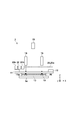
- FIG. 1 is a schematic diagram illustrating an imprint apparatus 1 according to the first embodiment.
- the imprint apparatus 1 includes a mold holding unit 12 that holds the mold 11, a substrate holding unit 14 that holds the substrate 13, a detection unit 15, a curing unit 21, an observation unit 23, an imaging unit 24, and a control unit. 26.
- the imprint apparatus 1 may also include a supply unit that supplies the imprint material 20 on the substrate, a bridge surface plate for holding the mold holding unit 12, a base surface plate for holding the substrate holding unit 14, and the like. .
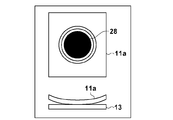
- the mold 11 is made of a material that can transmit light 21a (ultraviolet light) for curing the imprint material 20 such as quartz, and a pattern (unevenness) to be transferred to the imprint material 20 on the substrate. Pattern area 11a in which a pattern) is formed.
- the substrate 13 is, for example, a single crystal silicon substrate or an SOI (Silicon on Insulator) substrate, and the imprint material 20 is supplied (applied) to the upper surface (surface to be processed) of the substrate 13.
- the mold holding unit 12 includes, for example, a mold chuck that sucks the mold 11 by a vacuum suction force or an electrostatic suction force, a mold stage on which the mold chuck is placed, and a drive system that drives (moves) the mold stage. May be included.
- the drive system of the mold holding unit 12 drives the mold stage (that is, the mold 11) in at least the Z direction (the imprinting direction when imprinting the mold 11 on the imprint material 20 on the substrate). Further, the mold holding unit 12 has an opening 12 a for allowing the light 21 a emitted from the curing unit 21 to cure the imprint material 20 to pass therethrough.
- the drive system of the mold holding unit 12 in the first embodiment has a function of driving the mold stage not only in the Z direction but also in, for example, the X direction, the Y direction, and the ⁇ direction (rotation direction around the Z axis). May be.
- the substrate holding unit 14 includes, for example, a substrate chuck that attracts the substrate 13 by a vacuum attracting force or an electrostatic attracting force, a substrate stage on which the substrate chuck is placed, and a drive system that drives (moves) the substrate stage. May be included.
- the drive system of the substrate holding unit 14 drives the substrate stage (that is, the substrate 13) in at least the X direction and the Y direction (direction orthogonal to the stamping direction of the mold 11).
- the drive system of the substrate holding unit 14 in the first embodiment may have a function of driving the substrate stage not only in the X direction and the Y direction, but also in the Z direction and the ⁇ direction, for example.
- the detection unit 15 optically detects (observes) a mark 18 formed on the mold 11 (hereinafter referred to as a mold-side mark 18) and a mark 19 formed on the substrate 13 (hereinafter referred to as a substrate-side mark 19). Include the scope to be. And the detection part 15 calculates
- the detection unit 15 may not be able to detect the mark 18 on the mold side and the mark 19 on the substrate side at the same time. For example, the detection unit 15 obtains the position of the mold-side mark 18 and the position of the substrate-side mark 19 with respect to the reference position disposed therein, thereby obtaining a relative relationship between the mold-side mark 18 and the substrate-side mark 19. A specific positional relationship may be detected.
- the curing unit 21 irradiates the imprint material 20 on the substrate with light 21a (ultraviolet light) for curing the imprint material 20 through the opening 12a of the mold holding unit 12 and the mold 11, and the imprint material. 20 is cured.
- the curing unit 21 may include, for example, a light source that emits light 21a for curing the imprint material 20, and an optical system that adjusts the light 21a emitted from the light source to optimum light in the imprint process. .
- the imprint apparatus 1 according to the present embodiment can be configured such that the light 21a emitted from the curing unit 21 is reflected by the beam splitter 27 and irradiated onto the substrate 13 (imprint material 20).
- the observation unit 23 includes a camera having a field of view in which the entire pattern region 11a of the mold 11 can be accommodated, and has a function of observing (confirming) the cured state of the imprint material 20 on the substrate by irradiation with the light 21a.
- the observation unit 23 includes a foreign matter mixed state between the mold 11 and the substrate 13, a filling state of the imprint material 20 into the pattern region 11a of the mold 11, and the mold 11 from the cured imprint material 20 on the substrate. It is also possible to observe the mold release state. Furthermore, it is possible to observe the contact state between the mold 11 and the imprint material 20 supplied onto the substrate.
- the imprint apparatus 1 according to the present embodiment is configured such that the observation unit 23 observes the cured state of the imprint material 20 via the beam splitter 27.
- the control unit 26 includes, for example, a CPU and a memory, and controls imprint processing (controls each unit of the imprint apparatus 1).
- the control unit 26 performs imprint processing while aligning the mold 11 and the substrate 13 based on the detection result by the detection unit 15 (that is, the measurement result of the relative position between the mold 11 and the substrate 13).
- the control unit 26 obtains information related to the pattern formation of the imprint material 20 based on an image obtained by the imaging unit 24 described later.
- the information includes, for example, information on mixing of foreign matter between the mold 11 and the substrate 13, information on filling the imprint material 20 into the pattern of the mold 11, and information on overlaying the mold 11 and the substrate 13. At least one of them may be included.
- an optical system for forming an image of the observation region (images of the marks 18 and 19) in a space where the above-described component can be easily formed may be configured.
- the relay optical system includes a plurality of relay lenses 30.
- the relay lens 30 forms an image of the observation area outside the mold holding unit 12 as an image that is the same size or enlarged or reduced. Since the relay lens 30 may have a fixed configuration, the relay lens 30 may have only an optical member such as a lens and a member that holds the optical member.
- the 11 includes an optical member 31 for combining and separating detection light detected by the detection unit 15 and detection light for the light 21a and the observation unit 23.
- the optical member 31 may constitute an optical film having the property of reflection or transmission depending on the wavelength band, for example. In the configuration of FIG. 11, the light in the wavelength band used by the detection unit 15 is reflected and the light in the wavelength band used by the light 21 a and the observation unit 23 is transmitted.
- FIG. 2A is a diagram showing the pattern region 11a of the mold 11, specifically, marks 18a to 18h provided at the four corners of the pattern region 11a.
- marks 18a, 18b, 18f and 18e whose longitudinal direction is the X direction are marks whose measurement direction is the X direction
- marks 18c, 18d, 18g and 18h whose longitudinal direction is the Y direction are Y It is a mark whose direction is the measurement direction.
- FIG. 2A also shows a region 11b where a pattern to be transferred is formed on each of the six chip regions 13b on the substrate.
- FIG. 2B is a diagram showing marks 19a to 19h provided in one shot region 13a of the substrate 13.
- marks 19a, 19b, 19f and 19e whose longitudinal direction is the X direction are marks whose measurement direction is the X direction
- marks 19c, 19d, 19g and 19h whose longitudinal direction is the Y direction are Y It is a mark whose direction is the measurement direction.
- six chip regions 13b are shown.
- the detection unit 15 detects the relative positions of the marks 18a to 18h on the mold side and the corresponding marks 19a to 19h on the substrate side. .
- the shape and position of at least one of the pattern region 11a of the mold 11 and the shot region 13a of the substrate 13 are changed based on the detection result by the detection unit 15 so that each relative position becomes the target relative position. . Thereby, the pattern area 11a of the mold 11 and the shot area 13a of the substrate 13 can be accurately overlapped.
- FIGS. 3A to 3C are diagrams for explaining the imprint process.
- the imprint material 20 is supplied to a target shot area on the substrate (a target shot area to be imprinted from now on). Since the imprint material 20 generally used in the imprint apparatus has high volatility, it is preferable to supply the imprint material 20 onto the substrate immediately before performing the imprint process. However, when using the imprint material 20 having low volatility, the imprint material 20 may be supplied on the substrate in advance by a spin coater or the like. Further, after supplying the imprint material 20 onto the substrate, as described above, the relative position between the mold-side mark 18 and the substrate-side mark 19 is detected by the detection unit 15, and the mold 11 is based on the detection result. And the substrate 13 are aligned.
- the mold 11 and the imprint material 20 on the substrate are brought into contact with each other, and a predetermined time is passed in this state, so that the pattern of the mold 11 is reached. Is filled with the imprint material 20. Even at this time, it is preferable to detect the mark 18 on the mold side and the mark 19 on the substrate side by the detection unit 15 and align the mold 11 and the substrate 13 based on the detection result.
- the refractive index difference between the mold 11 and the imprint material 20 is small, it is difficult to detect the mold-side mark 18 by the detection unit 15 if the mold-side mark 18 is configured only by the concavo-convex structure. May be.
- a material having a refractive index or transmittance different from that of the mold 11 may be applied to the mark 18 on the mold side, or the refractive index of the mark 18 on the mold side may be changed by ion irradiation or the like.
- the mark 18 on the mold side can be detected by the detection unit 15.
- the curing unit 21 irradiates the imprint material 20 on the substrate with light 21a through the mold 11, and the imprint material 20 is Harden.
- the mold 11 is peeled (released) from the cured imprint material 20 on the substrate, as shown in FIG. 3C.
- a pattern can be formed on the imprint material 20 on the substrate (that is, the pattern of the mold 11 can be transferred onto the substrate).
- the imprint apparatus 1 in the imprint process, for example, foreign matter is mixed between the mold 11 and the substrate 13, or the imprint material is insufficiently filled in the uneven pattern of the mold 11. Sometimes. Since such a defect may be taken over by the next imprint process, it is preferable to detect it before the next imprint process.
- the state of the imprint material 20 on the substrate is observed (imaged) by the observation unit 23, and the defect is detected based on the observation result.
- the state of the imprint material 20 on the substrate includes, for example, a cured state of the imprint material 20 on the substrate, a mixed state of foreign matter between the mold 11 and the substrate 13, and an imprint on the pattern of the mold 11.
- At least one of the filling states of the material 20 may be included.
- the state of the imprint material 20 includes a contact state (imprinting process) between the mold 11 and the imprint material 20 on the substrate, a mold release state from the cured imprint material 20, and the like. May be included.
- the imprint apparatus it is preferable to increase the size of the shot region to which the pattern of the mold 11 is transferred in one imprint process in order to improve productivity.
- the observation unit 23 having a field of view in which the entire pattern region 11a of the mold 11 is accommodated observes the state of the imprint material 20 with sufficient resolution (that is, the imprint material 20 is Imaging) can be difficult.
- the imprint material 20 is Imaging
- the observation unit 23 having a field of view in which the entire pattern region 11a of the mold 11 is within the field of view can image the imprint material 20 on the substrate in contact with the mold 11 at an angle in the periphery of the pattern region 11a.
- the imprint material 20 filled in the plurality of concave portions in the concave / convex pattern of the mold 11 is imaged in an overlapping manner, and the detection accuracy of the imprint processing defect may be insufficient.
- the imprint apparatus 1 includes an imaging unit 24 having a plurality of imaging elements 24f arranged in a line along a first direction (for example, the Y direction), and a second direction different from the first direction. And a scanning unit 25 that scans the imaging unit 24 (for example, in the X direction).
- the imaging unit 24 and the scanning unit 25 can be provided inside the opening 12 a of the mold holding unit 12.
- the control unit 26 causes the imaging unit 24 to scan the imaging unit 24 on the substrate while the scanning unit 25 scans the imaging unit 24 in the second direction while the mold 11 and the imprint material 20 are in contact with each other.
- the imprint material 20 is imaged.
- control unit 26 can obtain information related to the molding of the imprint material 20 based on the image obtained by the imaging unit 24.
- the information includes, for example, information regarding the mixing of foreign matter between the mold 11 and the substrate 13, information regarding filling of the imprint material 20 into the pattern of the mold 11, and information regarding the overlay accuracy between the mold 11 and the substrate 13. At least one of them.
- the imaging unit 24 may image the imprint material 20 on the substrate via an optical member such as the beam splitter 27 or the relay lens 30.
- the imaging surface of the substrate 13 may be formed on the upper part of the mold holding unit 12 so that the imaging unit 24 captures an image.
- FIG. 4 is a schematic diagram (XZ sectional view) showing a configuration example of the imaging unit 24.
- the imaging unit 24 is configured by arranging a plurality of units illustrated in FIG. 4 in the Y direction.
- One unit includes, for example, a light source 24a, optical members 24b to 24d, a half mirror 24e, and an imaging element 24f (photoelectric conversion element). ) Is provided.
- the light source 24 a can emit light having a wavelength different from that of the light 21 a (ultraviolet light) that cures the imprint material 20.
- the light emitted from the light source 24a and transmitted through the optical member 24b is reflected by the half mirror 24e and passes through the optical member 24c. Then, the light reflected by the imprint material 20 (substrate 13) through the mold 11 passes through the optical member 24c, the half mirror 24e, and the optical member 24d, and enters the image sensor 24f. Thereby, the imaging part 24 can image the imprint material 20 (board
- the imaging unit 24 is preferably configured such that the length in the longitudinal direction (for example, the Y direction) in the imaging region is longer than the width of the pattern region 11a of the mold 11.
- the imaging unit 24 configured as described above captures an image of the entire imprint material 20 in contact with the pattern region 11 a of the mold 11 by being scanned only once in the second direction (X direction) by the scanning unit 25. be able to.
- the present invention is not limited to this, and the imaging unit 24 is configured to image the entire substrate 13 by scanning only once in the second direction, for example, as shown in FIG. 5A. It may be.
- the imaging unit 24 is configured to be able to image the entire shot region (the entire substrate 13) by scanning a plurality of times along the second direction. Also good.
- FIGS. 6A to 6D are diagrams for explaining imaging of the imprint material 20 by the imaging unit 24, and show an example in which the pattern of the mold 11 is transferred to the entire substrate 13 by one imprint process.
- the upper diagram is a view of the imprint apparatus 1 viewed from the side ( ⁇ Y direction side)
- the lower diagram is a diagram of the imprint apparatus 1 viewed from the top (Z direction side).
- the control unit 26 is omitted and the configuration of the mold holding unit 12 is simplified for easy understanding.
- the imaging unit 24 is disposed so as to pass between the mold 11 and the detection unit 15 in the scanning in the second direction (for example, the X direction).
- the scanning unit 25 includes an actuator such as a linear motor, for example, and scans (drives) the imaging unit 24 along the guide rail 25a extending in the second direction. Further, after the imprint material 20 is cured, the imaging unit 24 may be scanned and measured after the detection unit 15 is retracted.
- the control unit 26 causes the curing unit 21 to contact the imprint material 20 on the substrate via the mold 11 while the mold 11 and the imprint material 20 on the substrate are in contact with each other.
- the imprint material 20 is cured by irradiating light.
- the control unit 26 scans the imaging unit 24 in the X direction by the scanning unit 25 and scans the cured imprint material 20 with the imaging unit 24 as illustrated in FIGS. 6B and 2C. Let's take an image. 6A to 6D indicate a region where imaging of the imprint material 20 by the imaging unit 24 is completed. Then, as illustrated in FIG.
- the control unit 26 images the cured imprint material 20 by the imaging unit 24 and then ends the scanning of the imaging unit 24 by the scanning unit 25. In this way, by causing the imaging unit 24 to image the imprint material 20 while scanning the imaging unit 24, the control unit 26 makes the imprint in which the mold 11 (pattern region 11 a) is in contact and is cured by the curing unit 21. An image of the material 20 can be obtained from the imaging unit 24.
- the mold 11 is in contact with the imaging unit 24 having the plurality of imaging elements 24f arranged in the first direction while the scanning unit 25 scans in the second direction.
- the imaging unit 24 is caused to image the imprint material 20 on the substrate being processed.
- the same effect can be obtained by configuring the imaging unit 24 at the imaging position of the relay optical system (relay lens 30).
- an image of the observation region is formed outside the mold holding unit 12 with the relay lens 30. It is better to capture the image and capture the image with the imaging unit 24.
- FIG. 7 is a schematic diagram illustrating the imprint apparatus 2 according to the second embodiment.
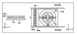
- the imprint apparatus 2 of the second embodiment includes a curing unit 22 having a plurality of light sources 22a arranged in a line along a first direction (for example, the Y direction).
- the curing unit 22 is scanned by the scanning unit 25 in the scanning direction (second direction (for example, the X direction) of the imaging unit 24.
- the scanning unit 25 is advantageous when the imprint material 20 on the substrate is partially cured.
- FIGS. 8A to 8C are diagrams showing a process of gradually increasing the contact area between the mold 11 and the imprint material 20.
- the upper view is a view of the mold 11 and the substrate 13 as viewed from above (Z direction side), and the lower view is a view of the mold 11 and the substrate 13 as viewed from the side ( ⁇ Y direction side).
- the black circle has shown the part (contact part 28) where the mold 11 and the imprint material 20 contacted.
- concentric lines on the outer periphery of the black region indicate interference fringes due to the mold and the substrate.
- the contact area of the imprinting force applied to the contact portion 28 between the mold 11 and the imprint material 20 gradually increases. It grows as it expands. Therefore, for example, if foreign matter is mixed in the contact portion 28 shown in FIG. 8A, the stress generated on the mold 11 and the substrate 13 by the foreign matter increases as the contact area gradually increases, and the mold 11 and the substrate 13 are destroyed. There is a risk of being. Therefore, it is preferable to detect a malfunction (for example, foreign matter) in the contact portion 28 at an early stage.
- the imprint apparatus 2 of the second embodiment applies the imprint material 20 to the curing unit 22 while scanning the curing unit 22 by the scanning unit 25 at each of a plurality of timings in the process of gradually increasing the contact area. Harden.
- the imaging unit 24 is caused to image the imprint material 20 cured by the curing unit 22 while scanning the imaging unit 24 by the scanning unit 25 at each of a plurality of timings.
- the imaging unit 24 in the present embodiment includes a first imaging unit 24a and a second imaging unit 24b each including a plurality of imaging elements 24f arranged in a line along the first direction (Y direction).
- the first imaging unit 24a and the second imaging unit 24b are arranged so as to sandwich the curing unit 22 in the second direction (X direction).
- the imaging unit 24 By configuring the imaging unit 24 in this way, even when the curing unit 22 and the imaging unit 24 are reciprocally scanned, the imprint material 20 cured by the curing unit 22 is converted into the first imaging unit 24a and the second imaging unit 24a. Any one of the imaging units 24b can perform imaging. Further, the scanning unit 25 in the present embodiment uses the guide rail 25a in common for the scanning of the imaging unit 24 and the scanning of the curing unit 22.
- FIGS. 9A to 9C are diagrams for explaining imaging of the imprint material 20 by the imaging unit 24.
- FIG. 9A to 9C the left figure shows the pattern region 11a and the substrate 13 of the mold 11 as viewed from the side (the ⁇ Y direction side), and the right figure shows the pattern region 11a and the substrate 13 of the mold 11 above. It is the figure seen from (Z direction side).
- 9A to 9C the hatched portion in the right figure corresponds to the contact portion 28 between the mold 11 and the imprint material 20.
- the detection unit 15 in the imprint apparatus 2 of the second embodiment can be configured to be movable.
- the control unit 26 detects the mold-side mark 18 and the substrate-side mark 19 in the contact portion 28 between the mold 11 and the imprint material 20 at a first timing in the process of gradually increasing the contact area. 15 to detect. Then, the mold 11 and the substrate 13 are aligned based on the detection result by the detection unit 15. After performing the alignment, the control unit 26 scans the curing unit 22 and the imaging unit 24 in the + X direction by the scanning unit 25 and scans the imprint material 20 of the contact portion 28 as illustrated in FIG. 9A. And the first imaging unit 24a images the substrate 13. At this time, the curing unit 22 can cure the imprint material 20 using only the light source 22a corresponding to the contact portion 28 among the plurality of light sources 22a.
- the scanning unit 25 causes the curing unit 22 and the imaging unit 24 to be scanned by the scanning unit 25
- the scanning of the imaging unit 24 follows the scanning of the curing unit 22.
- the scanning unit 25 may be controlled to be performed.
- the control unit 26 may control the scanning unit 25 so that the interval between the curing unit 22 and the imaging unit 24 is kept constant.
- control unit 26 detects the mold-side mark 18 and the substrate-side mark 19 in the contact portion 28 between the mold 11 and the imprint material 20 at the second timing when the contact area further increases. Let Then, the mold 11 and the substrate 13 are aligned based on the detection result by the detection unit 15. After the alignment, as shown in FIG. 9B, the control unit 26 scans the curing unit 22 and the imaging unit 24 in the ⁇ X direction by the scanning unit 25, and moves the imprint material 20 of the contact portion 28 to the curing unit.
- the second image pickup unit 24b causes the substrate 13 to pick up an image.
- control unit 26 causes the detection unit 15 to detect the mold-side mark 18 and the substrate-side mark 19 in the contact portion 28 between the mold 11 and the imprint material 20 at the third timing when the contact area further increases. . Then, the mold 11 and the substrate 13 are aligned based on the detection result by the detection unit 15. After the alignment, as shown in FIG. 9C, the control unit 26 scans the curing unit 22 and the imaging unit 24 in the + X direction by the scanning unit 25, and the imprint material 20 of the contact portion 28 is cured. And the first imaging unit 24a images the substrate 13.
- the imprint apparatus 2 By performing the imprint process in this manner, the imprint apparatus 2 according to the second embodiment causes the position of the mold 11 and the substrate 13 to be generated in the process of gradually increasing the contact area between the mold 11 and the imprint material 20. Deviation can be reduced. At the same time, it is possible to detect a malfunction (for example, foreign matter) in the contact portion 28 at an early stage.
- a malfunction for example, foreign matter
- the imprint material 20 of the contact portion 28 may be cured while the scanning unit 25 scans the curing unit, and the scanning of the imaging unit 24 may be started after the scanning of the curing unit 22 is completed.
- curing of the imprint material 20 by the curing unit 22 and imaging of the imprint material 20 by the imaging unit 24 are performed at each of a plurality of timings in the process of gradually increasing the contact area.
- the curing by the curing unit 22 and the imaging unit 24 are performed. You may perform imaging by. As described above, each time the contact area is expanded stepwise, only imaging may be performed, and curing may be performed after the transfer region is completely in contact.
- the pattern region 11a of the mold 11 is deformed into a convex shape has been described.
- the substrate 13 may be deformed into a convex shape facing the mold 11.
- FIGS. 10A and 10B are diagrams for explaining imaging of the imprint material 20 by the imaging unit 24 when the mold 11 and the imprint material 20 are brought into contact with each other from the end of the pattern region 11a.
- the left figure is a view of the imprint apparatus 2 viewed from the side ( ⁇ Y direction side)
- the right figure is a view of the imprint apparatus 2 viewed from the top (Z direction side).
- the boundary between the contact portion and the non-contact portion moves.
- the control unit 26 moves the detection unit 15 so as to follow the expansion of the contact area between the mold 11 and the imprint material 20 (that is, movement of the boundary), and the mold-side mark 18 and the substrate-side mark at the contact portion.
- the detection unit 15 sequentially detects the marks 19. Then, the control unit 26 aligns the mold 11 and the substrate 13 based on the detection result by the detection unit 15.
- control unit 26 scans the curing unit 22 and the imaging unit 24 by the scanning unit 25 so as to follow the expansion of the contact area (movement of the boundary), and the imprint material of the contact portion that has been aligned. 20 is sequentially cured to the curing unit 22.
- imaging unit 24 sequentially images the imprint material 20 cured by the curing unit 22.
- FIG. 12 is a diagram for explaining a region where a pattern is formed on the substrate 13 by a single imprint process.
- the A area shown in FIG. 12 shows one shot area.
- One shot area indicates an area where a pattern is formed by a lithography apparatus different from the imprint apparatus, for example.
- FIG. 12 shows a B area where imprint processing is performed simultaneously on two shot areas and a C area where imprint processing is performed simultaneously on four shot areas.
- the observation unit 23 decreases the image resolution because the area to be observed increases as the area to be simultaneously subjected to the imprint process increases. Therefore, the same effect can be obtained not only in the form in which the imprint process is performed on the entire surface of the substrate at once, but also in the form in which the imprint process is simultaneously performed on a plurality of shot areas.
- the method for manufacturing an article according to an embodiment of the present invention is suitable, for example, for manufacturing an article such as a microdevice such as a semiconductor device or an element having a fine structure.
- the method for manufacturing an article according to the present embodiment includes a step of forming a pattern on the imprint material supplied on the substrate using the imprint apparatus, and a step of processing the substrate on which the pattern is formed in such a step. Including. Further, the manufacturing method includes other well-known steps (oxidation, film formation, vapor deposition, doping, planarization, etching, resist stripping, dicing, bonding, packaging, and the like).
- the method for manufacturing an article according to the present embodiment is advantageous in at least one of the performance, quality, productivity, and production cost of the article as compared with the conventional method.
Landscapes
- Engineering & Computer Science (AREA)
- Mechanical Engineering (AREA)
- Physics & Mathematics (AREA)
- General Physics & Mathematics (AREA)
- Health & Medical Sciences (AREA)
- Environmental & Geological Engineering (AREA)
- Epidemiology (AREA)
- Public Health (AREA)
- Shaping Of Tube Ends By Bending Or Straightening (AREA)
- Exposure Of Semiconductors, Excluding Electron Or Ion Beam Exposure (AREA)
Priority Applications (1)
| Application Number | Priority Date | Filing Date | Title |
|---|---|---|---|
| KR1020197002514A KR102241655B1 (ko) | 2015-08-10 | 2017-01-26 | 임프린트 장치 및 물품 제조 방법 |
Applications Claiming Priority (3)
| Application Number | Priority Date | Filing Date | Title |
|---|---|---|---|
| JP2015158495 | 2015-08-10 | ||
| JP2016-132779 | 2016-07-04 | ||
| JP2016132779A JP6799397B2 (ja) | 2015-08-10 | 2016-07-04 | インプリント装置、および物品の製造方法 |
Publications (1)
| Publication Number | Publication Date |
|---|---|
| WO2018008174A1 true WO2018008174A1 (ja) | 2018-01-11 |
Family
ID=57994655
Family Applications (1)
| Application Number | Title | Priority Date | Filing Date |
|---|---|---|---|
| PCT/JP2017/002625 Ceased WO2018008174A1 (ja) | 2015-08-10 | 2017-01-26 | インプリント装置、および物品の製造方法 |
Country Status (5)
| Country | Link |
|---|---|
| US (1) | US10011057B2 (https=) |
| JP (1) | JP6799397B2 (https=) |
| KR (1) | KR102241655B1 (https=) |
| TW (1) | TWI737675B (https=) |
| WO (1) | WO2018008174A1 (https=) |
Families Citing this family (9)
| Publication number | Priority date | Publication date | Assignee | Title |
|---|---|---|---|---|
| JP6188382B2 (ja) * | 2013-04-03 | 2017-08-30 | キヤノン株式会社 | インプリント装置および物品の製造方法 |
| JP5960198B2 (ja) * | 2013-07-02 | 2016-08-02 | キヤノン株式会社 | パターン形成方法、リソグラフィ装置、リソグラフィシステムおよび物品製造方法 |
| US10353299B2 (en) * | 2016-06-01 | 2019-07-16 | Canon Kabushiki Kaisha | Lithography method, determination method, information processing apparatus, storage medium, and method of manufacturing article |
| JP7222623B2 (ja) * | 2018-07-23 | 2023-02-15 | キヤノン株式会社 | パターン形成方法および物品製造方法 |
| US11107678B2 (en) | 2019-11-26 | 2021-08-31 | Canon Kabushiki Kaisha | Wafer process, apparatus and method of manufacturing an article |
| KR102227885B1 (ko) * | 2020-06-02 | 2021-03-15 | 주식회사 기가레인 | 패턴 정렬 가능한 전사 장치 |
| JP7494037B2 (ja) * | 2020-07-15 | 2024-06-03 | キヤノン株式会社 | 情報処理装置、判定方法、検査装置、成形装置、および物品の製造方法 |
| KR102520642B1 (ko) * | 2020-12-29 | 2023-04-11 | 주식회사 기가레인 | 패턴 정렬 가능한 전사 장치 |
| JP7407465B2 (ja) * | 2022-03-04 | 2024-01-04 | 株式会社菊水製作所 | 成形品処理システム |
Citations (6)
| Publication number | Priority date | Publication date | Assignee | Title |
|---|---|---|---|---|
| US20070246850A1 (en) * | 2006-04-21 | 2007-10-25 | Molecular Imprints, Inc. | Method for Detecting a Particle in a Nanoimprint Lithography System |
| JP2011513973A (ja) * | 2008-02-26 | 2011-04-28 | モレキュラー・インプリンツ・インコーポレーテッド | リアルタイム・インプリント・プロセス欠陥診断法 |
| JP2015018997A (ja) * | 2013-07-12 | 2015-01-29 | 大日本印刷株式会社 | インプリント装置及びインプリント方法 |
| JP2015056589A (ja) * | 2013-09-13 | 2015-03-23 | キヤノン株式会社 | インプリント装置、インプリント方法、検出方法及びデバイス製造方法 |
| JP2015233071A (ja) * | 2014-06-09 | 2015-12-24 | キヤノン株式会社 | インプリント装置及び物品の製造方法 |
| JP2016201522A (ja) * | 2015-04-14 | 2016-12-01 | キヤノン株式会社 | インプリント装置、インプリント方法及び物品の製造方法 |
Family Cites Families (11)
| Publication number | Priority date | Publication date | Assignee | Title |
|---|---|---|---|---|
| GB2432029A (en) * | 2005-11-02 | 2007-05-09 | Crime Scene Invest Equipment L | Imprint identification system using image scanner calibration |
| US8345242B2 (en) * | 2008-10-28 | 2013-01-01 | Molecular Imprints, Inc. | Optical system for use in stage control |
| JP5173944B2 (ja) | 2009-06-16 | 2013-04-03 | キヤノン株式会社 | インプリント装置及び物品の製造方法 |
| JP5455583B2 (ja) | 2009-11-30 | 2014-03-26 | キヤノン株式会社 | インプリント装置 |
| JP5539011B2 (ja) * | 2010-05-14 | 2014-07-02 | キヤノン株式会社 | インプリント装置、検出装置、位置合わせ装置、及び物品の製造方法 |
| JP5597031B2 (ja) * | 2010-05-31 | 2014-10-01 | キヤノン株式会社 | リソグラフィ装置及び物品の製造方法 |
| JP5576822B2 (ja) * | 2011-03-25 | 2014-08-20 | 富士フイルム株式会社 | モールドに付着した異物の除去方法 |
| JP6039222B2 (ja) * | 2011-05-10 | 2016-12-07 | キヤノン株式会社 | 検出装置、検出方法、インプリント装置及びデバイス製造方法 |
| JP6071221B2 (ja) * | 2012-03-14 | 2017-02-01 | キヤノン株式会社 | インプリント装置、モールド、インプリント方法及び物品の製造方法 |
| JP6140990B2 (ja) * | 2012-11-30 | 2017-06-07 | キヤノン株式会社 | 測定装置、インプリントシステム、測定方法及びデバイス製造方法 |
| JP6083340B2 (ja) * | 2013-07-12 | 2017-02-22 | 富士通株式会社 | 化合物半導体装置及びその製造方法 |
-
2016
- 2016-07-04 JP JP2016132779A patent/JP6799397B2/ja active Active
- 2016-08-01 US US15/224,911 patent/US10011057B2/en active Active
-
2017
- 2017-01-26 WO PCT/JP2017/002625 patent/WO2018008174A1/ja not_active Ceased
- 2017-01-26 KR KR1020197002514A patent/KR102241655B1/ko active Active
- 2017-02-03 TW TW106103720A patent/TWI737675B/zh active
Patent Citations (6)
| Publication number | Priority date | Publication date | Assignee | Title |
|---|---|---|---|---|
| US20070246850A1 (en) * | 2006-04-21 | 2007-10-25 | Molecular Imprints, Inc. | Method for Detecting a Particle in a Nanoimprint Lithography System |
| JP2011513973A (ja) * | 2008-02-26 | 2011-04-28 | モレキュラー・インプリンツ・インコーポレーテッド | リアルタイム・インプリント・プロセス欠陥診断法 |
| JP2015018997A (ja) * | 2013-07-12 | 2015-01-29 | 大日本印刷株式会社 | インプリント装置及びインプリント方法 |
| JP2015056589A (ja) * | 2013-09-13 | 2015-03-23 | キヤノン株式会社 | インプリント装置、インプリント方法、検出方法及びデバイス製造方法 |
| JP2015233071A (ja) * | 2014-06-09 | 2015-12-24 | キヤノン株式会社 | インプリント装置及び物品の製造方法 |
| JP2016201522A (ja) * | 2015-04-14 | 2016-12-01 | キヤノン株式会社 | インプリント装置、インプリント方法及び物品の製造方法 |
Also Published As
| Publication number | Publication date |
|---|---|
| TW201802873A (zh) | 2018-01-16 |
| JP6799397B2 (ja) | 2020-12-16 |
| TWI737675B (zh) | 2021-09-01 |
| US20170043511A1 (en) | 2017-02-16 |
| KR20190022763A (ko) | 2019-03-06 |
| US10011057B2 (en) | 2018-07-03 |
| JP2017038042A (ja) | 2017-02-16 |
| KR102241655B1 (ko) | 2021-04-19 |
Similar Documents
| Publication | Publication Date | Title |
|---|---|---|
| JP6799397B2 (ja) | インプリント装置、および物品の製造方法 | |
| JP6360287B2 (ja) | リソグラフィ装置、位置合わせ方法、および物品の製造方法 | |
| KR101842394B1 (ko) | 임프린트 방법, 임프린트 장치 및 물품 제조 방법 | |
| KR101996771B1 (ko) | 임프린트 장치 및 물품 제조 방법 | |
| JP6271875B2 (ja) | インプリント装置、インプリント方法および物品の製造方法 | |
| KR101788362B1 (ko) | 임프린트 장치, 물품의 제조 방법 및 위치정렬 장치 | |
| KR101573572B1 (ko) | 임프린트 장치, 물품 제조 방법 및 패턴 전사 방법 | |
| KR102004624B1 (ko) | 패턴 성형 방법 및 물품의 제조 방법 | |
| JP2015233071A (ja) | インプリント装置及び物品の製造方法 | |
| JP2016063219A (ja) | インプリント装置、インプリントシステム及び物品の製造方法 | |
| CN104614937A (zh) | 压印设备 | |
| US12515946B2 (en) | Imprinting method, pre-processing apparatus, substrate for imprinting, and method for manufacturing substrate | |
| JP6560736B2 (ja) | インプリント装置、インプリント方法および物品の製造方法 | |
| US20150146207A1 (en) | Detection apparatus, imprint apparatus, and method of manufacturing article | |
| JP6604793B2 (ja) | インプリント装置および物品製造方法 | |
| TW202040645A (zh) | 計測裝置、圖案形成裝置及物品之製造方法 |
Legal Events
| Date | Code | Title | Description |
|---|---|---|---|
| 121 | Ep: the epo has been informed by wipo that ep was designated in this application |
Ref document number: 17823783 Country of ref document: EP Kind code of ref document: A1 |
|
| NENP | Non-entry into the national phase |
Ref country code: DE |
|
| ENP | Entry into the national phase |
Ref document number: 20197002514 Country of ref document: KR Kind code of ref document: A |
|
| 122 | Ep: pct application non-entry in european phase |
Ref document number: 17823783 Country of ref document: EP Kind code of ref document: A1 |