WO2018003283A1 - 弾性波装置及び電子部品 - Google Patents
弾性波装置及び電子部品 Download PDFInfo
- Publication number
- WO2018003283A1 WO2018003283A1 PCT/JP2017/017147 JP2017017147W WO2018003283A1 WO 2018003283 A1 WO2018003283 A1 WO 2018003283A1 JP 2017017147 W JP2017017147 W JP 2017017147W WO 2018003283 A1 WO2018003283 A1 WO 2018003283A1
- Authority
- WO
- WIPO (PCT)
- Prior art keywords
- acoustic wave
- wave device
- elastic wave
- elastic modulus
- wave element
- Prior art date
- Legal status (The legal status is an assumption and is not a legal conclusion. Google has not performed a legal analysis and makes no representation as to the accuracy of the status listed.)
- Ceased
Links
Images





Classifications
-
- H—ELECTRICITY
- H03—ELECTRONIC CIRCUITRY
- H03H—IMPEDANCE NETWORKS, e.g. RESONANT CIRCUITS; RESONATORS
- H03H9/00—Networks comprising electromechanical or electro-acoustic elements; Electromechanical resonators
- H03H9/02—Details
- H03H9/05—Holders or supports
- H03H9/10—Mounting in enclosures
- H03H9/1064—Mounting in enclosures for surface acoustic wave [SAW] devices
- H03H9/1078—Mounting in enclosures for surface acoustic wave [SAW] devices the enclosure being defined by a foil covering the non-active sides of the SAW device
-
- H—ELECTRICITY
- H03—ELECTRONIC CIRCUITRY
- H03H—IMPEDANCE NETWORKS, e.g. RESONANT CIRCUITS; RESONATORS
- H03H9/00—Networks comprising electromechanical or electro-acoustic elements; Electromechanical resonators
- H03H9/02—Details
- H03H9/02535—Details of surface acoustic wave devices
- H03H9/02818—Means for compensation or elimination of undesirable effects
- H03H9/02834—Means for compensation or elimination of undesirable effects of temperature influence
-
- H—ELECTRICITY
- H03—ELECTRONIC CIRCUITRY
- H03H—IMPEDANCE NETWORKS, e.g. RESONANT CIRCUITS; RESONATORS
- H03H9/00—Networks comprising electromechanical or electro-acoustic elements; Electromechanical resonators
- H03H9/02—Details
- H03H9/02535—Details of surface acoustic wave devices
- H03H9/02818—Means for compensation or elimination of undesirable effects
- H03H9/02897—Means for compensation or elimination of undesirable effects of strain or mechanical damage, e.g. strain due to bending influence
-
- H—ELECTRICITY
- H03—ELECTRONIC CIRCUITRY
- H03H—IMPEDANCE NETWORKS, e.g. RESONANT CIRCUITS; RESONATORS
- H03H9/00—Networks comprising electromechanical or electro-acoustic elements; Electromechanical resonators
- H03H9/02—Details
- H03H9/05—Holders or supports
- H03H9/0538—Constructional combinations of supports or holders with electromechanical or other electronic elements
- H03H9/0542—Constructional combinations of supports or holders with electromechanical or other electronic elements consisting of a lateral arrangement
-
- H—ELECTRICITY
- H03—ELECTRONIC CIRCUITRY
- H03H—IMPEDANCE NETWORKS, e.g. RESONANT CIRCUITS; RESONATORS
- H03H9/00—Networks comprising electromechanical or electro-acoustic elements; Electromechanical resonators
- H03H9/02—Details
- H03H9/05—Holders or supports
- H03H9/058—Holders or supports for surface acoustic wave devices
- H03H9/059—Holders or supports for surface acoustic wave devices consisting of mounting pads or bumps
-
- H—ELECTRICITY
- H03—ELECTRONIC CIRCUITRY
- H03H—IMPEDANCE NETWORKS, e.g. RESONANT CIRCUITS; RESONATORS
- H03H9/00—Networks comprising electromechanical or electro-acoustic elements; Electromechanical resonators
- H03H9/02—Details
- H03H9/05—Holders or supports
- H03H9/10—Mounting in enclosures
- H03H9/1064—Mounting in enclosures for surface acoustic wave [SAW] devices
- H03H9/1085—Mounting in enclosures for surface acoustic wave [SAW] devices the enclosure being defined by a non-uniform sealing mass covering the non-active sides of the SAW device
-
- H—ELECTRICITY
- H03—ELECTRONIC CIRCUITRY
- H03H—IMPEDANCE NETWORKS, e.g. RESONANT CIRCUITS; RESONATORS
- H03H9/00—Networks comprising electromechanical or electro-acoustic elements; Electromechanical resonators
- H03H9/02—Details
- H03H9/125—Driving means, e.g. electrodes, coils
- H03H9/145—Driving means, e.g. electrodes, coils for networks using surface acoustic waves
-
- H—ELECTRICITY
- H03—ELECTRONIC CIRCUITRY
- H03H—IMPEDANCE NETWORKS, e.g. RESONANT CIRCUITS; RESONATORS
- H03H9/00—Networks comprising electromechanical or electro-acoustic elements; Electromechanical resonators
- H03H9/25—Constructional features of resonators using surface acoustic waves
-
- H—ELECTRICITY
- H10—SEMICONDUCTOR DEVICES; ELECTRIC SOLID-STATE DEVICES NOT OTHERWISE PROVIDED FOR
- H10W—GENERIC PACKAGES, INTERCONNECTIONS, CONNECTORS OR OTHER CONSTRUCTIONAL DETAILS OF DEVICES COVERED BY CLASS H10
- H10W70/00—Package substrates; Interposers; Redistribution layers [RDL]
- H10W70/60—Insulating or insulated package substrates; Interposers; Redistribution layers
Definitions
- the present invention relates to an acoustic wave device in which an acoustic wave element is surrounded by a resin structure and an electronic component having the acoustic wave device.
- an acoustic wave element is mounted on a mounting substrate.
- the IDT electrode formation surface of the acoustic wave element is opposed to the upper surface of the mounting substrate with a gap.
- a sealing resin layer is provided so as to cover the surface and the side surface opposite to the IDT electrode formation surface of the acoustic wave element.
- the sealing resin layer has first to third sealing resin layers. The first sealing resin layer has the lowest elastic modulus and covers the surface and the side surface opposite to the IDT electrode formation surface of the acoustic wave element.
- the second sealing resin layer has the highest elastic modulus and is laminated on the outside of the first sealing resin layer.
- the third sealing resin layer has a higher elastic modulus than the first sealing resin layer, and a lower elastic modulus than the second sealing resin layer.
- the third sealing resin layer is laminated on the outside of the second sealing resin layer.
- an elastic wave element is covered with a first sealing resin layer having a low elastic modulus. For this reason, when an external force or a thermal shock is applied, the acoustic wave element moves, which may cause a disconnection of the wiring.
- An object of the present invention is to provide an elastic wave device and an electronic component in which even if an external force or a thermal shock is applied, an elastic wave element is difficult to move and a frequency characteristic is hardly changed.
- An elastic wave device includes an elastic wave element substrate having an IDT electrode forming surface and an IDT electrode provided on the IDT electrode forming surface, and first and second opposing each other.
- the body has a high elastic modulus resin portion having a relatively high elastic modulus and a low elastic modulus resin portion having a relatively low elastic modulus, and the low elastic modulus resin portion is formed on a side surface of the elastic wave element substrate.
- the IDT electrode forming surface side is provided in a region that does not reach the surface opposite to the IDT electrode forming surface, and is in contact with the side surface of the acoustic wave element substrate in the resin structure.
- the remaining resin portion of the portion is the high modulus resin It is.
- the IDT electrode formation surface of the acoustic wave element substrate and the first main surface of the resin structure are flush with each other. In this case, even if the wiring straddling the IDT electrode forming surface and the first main surface of the resin structure is provided, no stress concentration occurs because there is no bent portion in the wiring, and the wiring is disconnected. Is even less likely to occur.
- the IDT electrode formation surface of the acoustic wave element substrate is not flush with the first main surface of the resin structure.
- the resin structure has a through electrode penetrating from the first main surface toward the second main surface, and the first main surface.
- a first electrode is provided on the surface and connected to the through electrode, and the first electrode is electrically connected to the acoustic wave element.
- the resin structure includes a plurality of second electrodes provided on the second main surface and connected to the through electrodes.
- a plurality of the first electrodes are provided on the first main surface, and the density of the plurality of second electrodes is lower than the density of the plurality of first electrodes.
- electrical connection to the outside can be easily performed using the plurality of second electrodes on the second main surface side of the resin structure.
- the low elastic modulus resin portion is provided so as to reach the IDT electrode forming surface of the elastic wave element substrate.
- the IDT electrode formation surface of the acoustic wave element is connected to the first electrode and from the first main surface of the resin structure.
- a wiring electrode is further provided.
- the wiring electrode is provided so as to reach the low elastic modulus resin portion reaching the IDT electrode forming surface.
- thermal stress is concentrated at the boundary between the resin structure and the acoustic wave element, but if a wiring is directly present at the boundary, the stress is also directly applied to the wiring. On the other hand, if the low elastic modulus resin portion exists between them, the thermal stress applied to the wiring is alleviated. Therefore, disconnection of the wiring electrode is less likely to occur.
- the acoustic wave element substrate is a piezoelectric substrate.
- the elastic wave element substrate is provided on the piezoelectric thin film and one surface of the piezoelectric thin film, and propagates more than the elastic wave propagating through the piezoelectric thin film.
- a high sound speed member having a high sound speed of the bulk wave.
- a bulk wave is provided between the high acoustic velocity member and the piezoelectric thin film and propagates more than the acoustic velocity of the elastic wave propagating through the piezoelectric thin film.
- a low sound speed member having a low sound speed is further provided.
- an electronic component laminated on the second main surface of the resin structure is further provided.
- An electronic component according to the present invention includes a mounting substrate having a mounting surface, and an acoustic wave device configured according to the present invention mounted on the mounting surface of the mounting substrate.
- the present invention it is possible to provide an elastic wave device and an electronic component in which even if an external force or a thermal shock is applied, the elastic wave element hardly moves and the frequency characteristic hardly changes.
- FIG. 1 is a front sectional view of an acoustic wave device according to a first embodiment of the present invention.
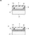
- FIG. 2A to FIG. 2C are front sectional views for explaining a manufacturing process of the acoustic wave device according to the first embodiment.
- FIG. 3A and FIG. 3B are front sectional views for explaining a manufacturing process of the acoustic wave device according to the first embodiment.
- FIG. 4A to FIG. 4C are front sectional views for explaining a manufacturing process of the acoustic wave device according to the first embodiment.
- FIG. 5 is a front sectional view for explaining a manufacturing process of the acoustic wave device according to the first embodiment of the present invention.
- FIG. 6 is a front sectional view of an acoustic wave device according to a second embodiment of the present invention.
- FIG. 7A and FIG. 7B are plan views schematically showing electrode structures of the first main surface and the second main surface of the resin structure.
- FIG. 8 is a front cross-sectional view of an electronic component according to the third embodiment of the present invention.
- FIG. 9 is a front sectional view of an electronic component according to the fourth embodiment of the present invention.
- FIG. 10 is a front sectional view of an acoustic wave device according to a fifth embodiment of the present invention.
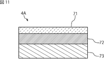
- FIG. 11 is a front sectional view for explaining a modification of the acoustic wave element substrate in the acoustic wave device of the present invention.
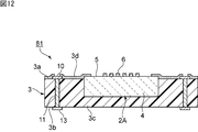
- FIG. 12 is a front sectional view of an acoustic wave device according to a sixth embodiment of the present invention.
- FIG. 1 is a front sectional view showing an acoustic wave device according to a first embodiment of the present invention.
- the elastic wave device 1 includes a plate-like elastic wave element 2 and a resin structure 3.
- the acoustic wave element 2 has an acoustic wave element substrate 4.
- the acoustic wave element substrate 4 is made of a piezoelectric body.
- the piezoelectric body to be used is not particularly limited, and piezoelectric single crystals such as LiNbO 3 and LiTaO 3 or piezoelectric ceramics can be used.
- the acoustic wave element substrate 4 has an IDT electrode forming surface 5.
- An IDT electrode 6 is provided on the IDT electrode formation surface 5.
- the acoustic wave element substrate 4 has a surface 7 that faces the IDT electrode formation surface 5 and side surfaces 8 a and 8 b that connect the IDT electrode formation surface 5 and the surface 7. Although not clearly shown in FIG. 1, the acoustic wave element substrate 4 has a rectangular planar shape. Therefore, the acoustic wave element substrate 4 has another set of side surfaces in addition to the opposing side surfaces 8a and 8b.
- the resin structure 3 has first and second main surfaces 3a and 3b facing each other.
- the resin structure 3 has a plate shape. But the resin structure 3 may have shapes other than plate shape.
- the acoustic wave element 2 is embedded in the resin structure 3 so that at least a part of the IDT electrode formation surface 5 is exposed. In the present embodiment, the IDT electrode formation surface 5 is flush with the first main surface 3a.
- the resin structure 3 has a high elastic modulus resin portion 3c having a relatively high elastic modulus and a low elastic modulus resin portion 3d having a relatively low elastic modulus.
- the elastic modulus mainly means Young's modulus.
- the low elastic modulus resin portion 3 d is provided so as to be in contact with part of the side surfaces 8 a and 8 b of the acoustic wave element substrate 4. More specifically, the low elastic modulus resin portion 3d extends downward from the end portions 8a1 and 8b1 of the side surfaces 8a and 8b on the IDT electrode forming surface side in the side surfaces 8a and 8b, provided that the side surfaces 8a and 8b and the surface 7 It is provided in a region that does not reach the edge formed by.
- the low elastic modulus resin portion 3d does not reach the surface 7 on the opposite side of the IDT electrode formation surface 5 from the end portions 8a1 and 8b1 on the IDT electrode formation surface side on the side surfaces 8a and 8b of the acoustic wave element substrate 4. Since the remaining resin portion of the resin structure 3 in contact with the side surfaces 8a and 8b of the elastic wave element substrate 4 is the high elastic modulus resin portion 3c, external force and heat Even if an impact is applied, the elastic wave device 1 can be provided in which the elastic wave element 2 hardly moves and the frequency characteristics hardly change.
- the length from the end portions 8a1 and 8b1 of the side surfaces 8a and 8b on the IDT electrode forming surface side to the lower end of the low elastic modulus resin portion 3d is x.
- the height dimension of the side surfaces 8a and 8b that is, the distance between the IDT electrode forming surface 5 and the surface 7 is y
- x ⁇ y preferably x is (1/2) or less of y. It is desirable that This is because the force for detaching the acoustic wave element substrate 4 from the resin structure 3 may rapidly decrease when the side coverage with the high elastic modulus resin portion 3c exceeds 1/2.
- a low elastic modulus resin portion is provided so as to come into contact with the side surface even in another set of side surfaces not shown.
- the resin portion other than the portion where the low elastic modulus resin portion 3d is provided is the above-described high elastic modulus resin portion 3c.
- the low elastic modulus resin portion 3d is made of an appropriate resin having a lower elastic modulus than the high elastic modulus resin portion 3c.
- a resin a material mainly composed of one of polyimide, polybenzoxazole, silicone resin, polyimide amide, and polyurethane is preferably used.
- the high elastic modulus resin portion 3c is made of an appropriate resin material having a higher elastic modulus than the low elastic modulus resin portion 3d.
- a resin material a synthetic resin such as an epoxy resin, or a material mainly composed of an inorganic material mixed with a resin can be used.
- the high elastic modulus resin portion 3c has an elastic modulus of 5 GPa or more. In that case, in the acoustic wave device 1, the acoustic wave element 2 can be more reliably protected.
- the elastic modulus of the low elastic modulus resin portion 3d is preferably 3 Gpa or less. In that case, it is possible to more effectively suppress deterioration of the characteristics of the acoustic wave device 2 due to externally applied stress. The disconnection etc. which are mentioned later are hard to produce further.
- the above elastic modulus is a value specified by a mechanical test method.
- the first electrode 10 is provided on the first main surface 3 a of the resin structure 3.
- a via electrode 11 as a through electrode is provided in the resin structure 3 so as to be electrically connected to the first electrode 10.
- the via electrode 11 penetrates the resin structure 3 from the first main surface 3a toward the second main surface 3b.
- a second electrode 13 is provided on the second main surface 3b. The second electrode 13 is provided to electrically connect the acoustic wave device 1 to the outside.
- a wiring electrode 14 is provided so as to be electrically connected to the first electrode 10.
- the wiring electrode 14 is electrically connected to the IDT electrode 6 at a portion not shown.
- the low elastic modulus resin portion 3d extends over the first main surface 3a and the IDT electrode formation surface 5 beyond the end portions 8a1 and 8b1 of the side surfaces 8a and 8b on the IDT electrode formation surface side. Has reached.
- the film-like portion 3d1 reaching the first main surface 3a and the IDT electrode formation surface 5 is provided so as to straddle the first main surface 3a and the IDT electrode formation surface 5.
- the wiring electrode 14 reaches the IDT electrode formation surface 5 through the film-like portion 3d1.
- the characteristics of the acoustic wave element 2 fluctuate due to the piezoelectric effect.
- the energy of the surface acoustic wave excited by the IDT electrode 6 is concentrated in the vicinity of the IDT electrode formation surface 5. Therefore, the side surfaces 8a and 8b of the acoustic wave element substrate 4 are provided in regions that do not reach the surface 7 on the opposite side of the IDT electrode formation surface 5 from the end portions 8a1 and 8b1 on the IDT electrode formation surface side.
- the elastic modulus resin portion 3d can effectively suppress fluctuations in frequency characteristics due to external force or thermal shock. Therefore, in the acoustic wave device 1, even when an external force or a thermal shock is applied, the frequency characteristics are hardly changed.
- the wiring electrode 14 passes over the film-like portion 3d1 of the low elastic modulus resin portion 3d and reaches the IDT electrode forming surface 5. Therefore, even if the external force as described above is applied, or even if distortion is applied due to a difference in linear expansion coefficient between the resin structure 3 and the acoustic wave element substrate 4 due to thermal stress, disconnection in the wiring electrode 14 is unlikely to occur. .
- a high elastic modulus resin portion 3 c exists in the lower part of the side surfaces 8 a and 8 b of the acoustic wave element substrate 4 and around the surface 7. Therefore, the elastic wave element 2 can be reliably protected from external thermal shock and external force. In addition, since the elastic wave element 2 is embedded in the resin structure 3, the size can be reduced.
- FIG. 1 An example of a method for manufacturing the acoustic wave device 1 will be described with reference to FIGS. 2 (a) to 2 (c) to 5.
- FIG. 2 (a) to 2 (c) to 5 An example of a method for manufacturing the acoustic wave device 1 will be described with reference to FIGS. 2 (a) to 2 (c) to 5.
- FIG. 2 (a) to 2 (c) to 5 An example of a method for manufacturing the acoustic wave device 1 will be described with reference to FIGS. 2 (a) to 2 (c) to 5.
- a resist layer 22 is formed on the support substrate 21.
- a metal film 23 is formed on the resist layer 22.
- a metal layer 11A to be the via electrode 11 is provided on the metal film 23 by photolithography or the like.
- a temporarily fixed resin layer 24 is provided.
- the elastic wave element substrate 4 is press-fitted onto the temporarily fixed resin layer 24.
- the elastic wave element 2 is press-fitted so that the IDT electrode formation surface 5 becomes the lower surface.
- a high elastic modulus resin portion 3 c is formed so as to cover the acoustic wave element substrate 4.
- the high elastic modulus resin portion 3c is polished to expose the metal layer 11A.
- the support substrate 21 is peeled off together with the resist layer 22.
- the high elastic modulus resin portion 3c and the via electrode 11 positioned in the high elastic modulus resin portion 3c are formed.
- the temporarily fixed resin layer 24 is removed using a solvent.
- a low elastic modulus resin portion 3d is formed.
- an IDT electrode 6, a first electrode 10, a second electrode 13, and a wiring electrode 14 are provided. In this way, the elastic wave device 1 of the first embodiment can be obtained.
- FIG. 6 is a front sectional view of the acoustic wave device according to the second embodiment of the present invention.
- the elastic wave device 31 includes an elastic wave element 2, an electronic component 32, and a resin structure 3.
- the acoustic wave element 2 is configured in the same manner as the acoustic wave element 2 of the first embodiment. Accordingly, the same parts are denoted by the same reference numerals, and the description thereof is omitted.
- the electronic component 32 is an electronic component different from the acoustic wave element 2.
- the resin structure 3 includes a low elastic modulus resin portion 3d and a high elastic modulus resin portion 3c.
- the low elastic modulus resin portion 3 d reaches not only a part of the side surfaces 8 a and 8 b of the acoustic wave element substrate 4 but also the IDT electrode formation surface 5. Also in the present embodiment, since the resin structure 3 includes the low elastic modulus resin portion 3d and the high elastic modulus resin portion 3c, the characteristics are hardly changed when an external force is applied, as in the first embodiment. In addition, disconnection of the wiring electrode 14 and the like is difficult to occur. Furthermore, the acoustic wave element 2 can be reliably protected from the outside by the presence of the high elastic modulus resin portion 3c.
- the other electronic component 32 is also provided in the resin structure 3, it is possible to reduce the size of the composite component including the acoustic wave element 2 and the electronic component 32. Also in the electronic component 32, the low elastic modulus resin portion 3d is provided so as to contact a part of the side surface. Therefore, even in the electronic component 32, disconnection of the wiring electrode is difficult to occur.
- an active element such as a semiconductor device or a passive element such as a capacitor can be used.
- the characteristic change due to the external force hardly occurs, but the disconnection or the like can be effectively suppressed by the presence of the low elastic modulus resin portion 3d.
- FIG. 7A and 7B are plan views schematically showing the electrode structure of the first main surface 3a and the second main surface 3b of the resin structure 3.
- FIG. 7A a plurality of first electrodes 10, 10, 10 are provided on one short side and the other short side of the first main surface 3a, respectively.
- the first electrodes 10, 10, 10 on one short side are electrically connected to the acoustic wave element 2.
- the other first electrode 10, 10, 10 on the other short side is electrically connected to the electronic component 32.
- the first electrode 10 is electrically connected to the second electrode 13 through the via electrode 11.
- the terminal electrode 13 ⁇ / b> A having a larger area than the second electrode 13 is connected to the second electrode 13.
- the terminal electrode 13A is provided at a position overlapping the acoustic wave element 2 and the electronic component 32 in the vertical direction. Therefore, the elastic wave device 31 can be easily electrically connected to the outside using the terminal electrode 13A having a relatively large area.
- the electrode density on the second main surface 3b side is lower than the electrode density on the first main surface 3a. Therefore, the large terminal electrode 13A as described above can be easily formed.
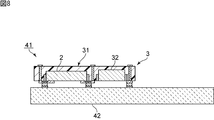
- FIG. 8 is a front sectional view of an electronic component according to the third embodiment of the present invention.
- the acoustic wave device 31 of the second embodiment is mounted on the mounting surface of the mounting substrate 42.
- the elastic wave device 31 may be mounted on the mounting surface of the mounting substrate 42.
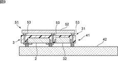
- FIG. 9 is a front sectional view of an electronic component according to the fourth embodiment of the present invention.
- an electronic component 52 is further stacked on the electronic component 41 of the third embodiment.
- the electronic component 52 may be an acoustic wave device, an active element such as a semiconductor device, or a passive component such as a capacitor or an inductor.
- the electronic component 52 is stacked on the elastic wave device 31 using a plurality of bumps 53.
- the mounting substrate 42 may be omitted. That is, in the present invention, a structure in which the electronic component 52 is stacked on the elastic wave device 31 described above may be used.
- FIG. 10 is a front sectional view of an acoustic wave device according to a fifth embodiment of the present invention.
- the thickness of the acoustic wave element substrate 4 of the acoustic wave element 2A is increased. That is, the IDT electrode formation surface 5 protrudes outward in the thickness direction from the first main surface 3 a of the resin structure 3.
- the IDT electrode formation surface 5 and the first main surface 3a may not be flush with each other but may be separated from each other by a step.
- the IDT electrode forming surface 5 and the first main surface 3a are preferably flush with each other. In that case, even if a wiring straddling the IDT electrode formation surface 5 and the first main surface 3a of the resin structure 3 is provided, stress concentration does not occur because there is no bent portion in the wiring. Wiring breakage is less likely to occur.
- the IDT electrode forming surface 5 may be located at a position indicated by a dashed line A in FIG. In this case, the IDT electrode formation surface 5 is located on the inner side in the thickness direction of the resin structure 3 than the first main surface 3a. Even in such a case, the same effect as the elastic wave device 1 of the first embodiment can be obtained by the presence of the low elastic modulus resin portion 3d and the high elastic modulus resin portion 3c. That is, it is difficult for the characteristics to change when an external force is applied. In addition, the acoustic wave element 2A can be reliably protected from the outside.
- the acoustic wave elements 2 and 2A have the acoustic wave element substrate 4 made of a piezoelectric body.
- the low sound velocity layer 72 and the high sound velocity layer 73 may be laminated.
- the low acoustic velocity layer 72 is made of a material having a lower acoustic velocity of the bulk wave propagating than the elastic wave propagating through the piezoelectric thin film 71.
- the high sound velocity layer 73 is made of a material in which the sound velocity of the propagating bulk wave is higher than that of the elastic wave propagating through the piezoelectric thin film 71.
- a laminated body in which low acoustic impedance layers and high acoustic impedance layers are alternately laminated may be laminated on the piezoelectric thin film 71.
- the electrical characteristics may fluctuate due to the piezoelectric effect. There is. Therefore, by using the resin structure having the low modulus resin portion and the high modulus resin portion of the present invention, the same effects as those of the first to fifth embodiments can be obtained.
- FIG. 12 is a front sectional view of an acoustic wave device according to a sixth embodiment of the present invention.
- the low elastic modulus resin portion 3 d is provided so as to be in contact with the upper end portion of the side surface of the elastic wave element substrate 4.
- the low elastic modulus resin portion 3d is exposed on the upper surface of the resin structure 3, and is provided so as to extend from the upper surface of the high elastic modulus resin portion 3c to the upper surface of the acoustic wave element substrate 4.
- the low elastic modulus resin portion 3d is provided on the side surface of the acoustic wave element substrate 4 in a region that does not reach the opposite surface from the end portion on the IDT electrode formation surface 5 side.
- the high elastic modulus resin portion 3 c is in contact with the remaining portion of the side surface of the elastic wave element substrate 4. Therefore, in the sixth embodiment, the same effect as in the first to fifth embodiments can be obtained.
Landscapes
- Physics & Mathematics (AREA)
- Acoustics & Sound (AREA)
- Surface Acoustic Wave Elements And Circuit Networks Thereof (AREA)
- Structures Or Materials For Encapsulating Or Coating Semiconductor Devices Or Solid State Devices (AREA)
Abstract
外力や熱衝撃が加わったとしても、弾性波素子が移動し難く、周波数特性の変化が生じ難い、弾性波装置を提供する。 板状の弾性波素子2と樹脂構造体3とを備える弾性波装置1。樹脂構造体3が、相対的に弾性率が高い高弾性率樹脂部3cと、相対的に弾性率が低い低弾性率樹脂部3dとを有する。弾性波素子基板4の側面8a,8bにおいて、IDT電極形成面側の端部8a1,8b1から、IDT電極形成面5の反対側の面7には至らない領域に、低弾性率樹脂部3dが設けられており、樹脂構造体3の弾性波素子基板4の側面に接触している部分のうち残りの樹脂部分が高弾性率樹脂部3cである。
Description
本発明は、樹脂構造体により弾性波素子が囲まれている弾性波装置及び該弾性波装置を有する電子部品に関する。
従来、弾性波素子のIDT電極形成面を除く部分を樹脂で封止した構造が知られている。下記の特許文献1に記載の弾性波装置では、弾性波素子が実装基板上に実装されている。弾性波素子のIDT電極形成面が実装基板の上面と隙間を隔てて対向されている。弾性波素子のIDT電極形成面とは反対側の面及び側面を覆うように、封止樹脂層が設けられている。特許文献1では、封止樹脂層が、第1~第3の封止樹脂層を有している。第1の封止樹脂層は、弾性率が最も低く、弾性波素子のIDT電極形成面とは反対側の面及び側面を被覆している。第2の封止樹脂層は、最も弾性率が高く、第1の封止樹脂層の外側に積層されている。第3の封止樹脂層は、第1の封止樹脂層よりも弾性率が高く、第2の封止樹脂層よりも弾性率が低い。第3の封止樹脂層は、第2の封止樹脂層の外側に積層されている。
特許文献1に記載の弾性波装置では、弾性波素子が低弾性率の第1の封止樹脂層により覆われている。そのため、外力や熱衝撃が加わると、弾性波素子が移動し、それによって配線の断線などが生じるおそれがあった。
他方、弾性波素子の外力による移動を抑制するには、弾性波素子に直接接触する封止樹脂層を、高弾性率の封止樹脂で形成することが考えられる。しかしながら、その場合には、外力が加わると、弾性波素子に大きな応力が加わる。そのため、弾性波素子の圧電体が歪み、弾性波素子の周波数特性が変化するという問題が生じる。
本発明の目的は、外力や熱衝撃が加わったとしても、弾性波素子が移動し難く、周波数特性の変化が生じ難い、弾性波装置及び電子部品を提供することにある。
本発明に係る弾性波装置は、IDT電極形成面を有する弾性波素子基板と、前記IDT電極形成面に設けられたIDT電極とを有する、弾性波素子と、対向し合う第1及び第2の主面を有し、前記第1の主面側において、前記IDT電極形成面の少なくとも一部が露出するように、前記弾性波素子が埋め込まれている樹脂構造体と、を備え、前記樹脂構造体が、相対的に弾性率が高い高弾性率樹脂部と、相対的に弾性率が低い低弾性率樹脂部とを有し、前記低弾性率樹脂部は、前記弾性波素子基板の側面において、前記IDT電極形成面側の端部から、前記IDT電極形成面の反対側の面には至らない領域に設けられており、前記樹脂構造体における前記弾性波素子基板の側面に接触している部分のうち残りの樹脂部分が前記高弾性率樹脂部である。
本発明に係る弾性波装置のある特定の局面では、前記弾性波素子基板の前記IDT電極形成面と、前記樹脂構造体の前記第1の主面とが面一とされている。この場合には、IDT電極形成面と、樹脂構造体の第1の主面とに跨る配線が設けられていたとしても、配線に屈曲部が存在しないため応力集中が起こらず、該配線の断線がより一層生じ難い。
本発明に係る弾性波装置の別の特定の局面では、前記弾性波素子基板の前記IDT電極形成面が、前記樹脂構造体の前記第1の主面と面一ではない。
本発明に係る弾性波装置の別の特定の局面では、前記樹脂構造体が、前記第1の主面から前記第2の主面に向かって貫通している貫通電極と、前記第1の主面に設けられており、前記貫通電極に接続されている第1の電極を有し、前記第1の電極が、前記弾性波素子に電気的に接続されている。
本発明に係る弾性波装置のさらに他の特定の局面では、前記樹脂構造体が、前記第2の主面に設けられており、前記貫通電極に接続されている複数の第2の電極を備え、前記第1の電極が、前記第1の主面に複数設けられており、前記複数の第1の電極の密度よりも、前記複数の第2の電極の密度が低くされている。この場合には、樹脂構造体の第2の主面側の複数の第2の電極を利用して、外部と電気的接続を容易に行うことができる。
本発明に係る弾性波装置のさらに他の特定の局面では、前記低弾性率樹脂部が、前記弾性波素子基板の前記IDT電極形成面上に至るように設けられている。
本発明に係る弾性波装置のさらに他の特定の局面では、前記第1の電極に接続されており、前記樹脂構造体の前記第1の主面上から前記弾性波素子の前記IDT電極形成面に至る配線電極がさらに備えられている。
本発明に係る弾性波装置の別の特定の局面では、前記配線電極が前記IDT電極形成面に至っている前記低弾性率樹脂部上に至るように設けられている。
一般的に、樹脂構造体と弾性波素子との境界部に熱応力が集中するが、その部分に直接配線が存在していると、その応力も直接配線に加わる。これに対して、低弾性率樹脂部が間に存在していると配線に加わる熱応力が緩和される。従って、配線電極の断線がより一層生じ難い。
本発明に係る弾性波装置の他の特定の局面では、前記弾性波素子基板が、圧電基板である。
本発明に係る弾性波装置のさらに他の特定の局面では、前記弾性波素子基板が、圧電薄膜と、前記圧電薄膜の一方面に設けられており、前記圧電薄膜を伝搬する弾性波よりも伝搬するバルク波の音速が高速である、高音速部材とを有する。
本発明に係る弾性波装置のさらに他の特定の局面では、前記高音速部材と、前記圧電薄膜との間に設けられており、前記圧電薄膜を伝搬する弾性波の音速よりも伝搬するバルク波の音速が低速である、低音速部材がさらに備えられている。
本発明に係る弾性波装置の別の特定の局面では、前記樹脂構造体の前記第2の主面上に積層された電子部品がさらに備えられている。
本発明に係る電子部品は、実装面を有する実装基板と、前記実装基板の前記実装面上に実装された本発明に従って構成された弾性波装置とを備える。
本発明によれば、外力や熱衝撃が加わったとしても、弾性波素子の移動が生じ難く、周波数特性の変化が生じ難い、弾性波装置及び電子部品を提供することができる。
以下、図面を参照しつつ、本発明の具体的な実施形態を説明することにより、本発明を明らかにする。
なお、本明細書に記載の各実施形態は、例示的なものであり、異なる実施形態間において、構成の部分的な置換または組み合わせが可能であることを指摘しておく。
図1は、本発明の第1の実施形態に係る弾性波装置を示す正面断面図である。弾性波装置1は、板状の弾性波素子2と、樹脂構造体3とを備える。弾性波素子2は、弾性波素子基板4を有する。本実施形態では、弾性波素子基板4は、圧電体からなる。使用する圧電体は特に限定されず、LiNbO3やLiTaO3などの圧電単結晶、または圧電セラミックスを用いることができる。
弾性波素子基板4は、IDT電極形成面5を有する。IDT電極形成面5上に、IDT電極6が設けられている。
弾性波素子基板4は、IDT電極形成面5と対向する面7と、IDT電極形成面5と面7とを結ぶ側面8a,8bとを有する。図1では明瞭ではないが、弾性波素子基板4は矩形の平面形状を有している。従って、弾性波素子基板4は、対向し合う側面8a,8bの他に、他の1組の側面を有する。
樹脂構造体3は、対向し合う第1及び第2の主面3a,3bを有する。本実施形態では、樹脂構造体3は、板状の形状を有している。もっとも、樹脂構造体3は、板状以外の形状を有していてもよい。弾性波素子2は、IDT電極形成面5の少なくとも一部を露出するようにして、樹脂構造体3に埋め込まれている。本実施形態では、IDT電極形成面5が、第1の主面3aと面一とされている。
樹脂構造体3は、相対的に弾性率が高い高弾性率樹脂部3cと、相対的に弾性率が低い低弾性率樹脂部3dとを有する。なお、弾性率とは、主としてヤング率を意味している。低弾性率樹脂部3dは、弾性波素子基板4の側面8a,8bの一部に接するように設けられている。より具体的には、低弾性率樹脂部3dは、側面8a,8bにおいて、側面8a,8bのIDT電極形成面側の端部8a1,8b1から下方に延び、但し、側面8a,8bと面7とのなす端縁には至らない領域に設けられている。
すなわち、低弾性率樹脂部3dが、弾性波素子基板4の側面8a,8bにおいて、IDT電極形成面側の端部8a1,8b1から、IDT電極形成面5の反対側の面7には至らない領域に設けられており、樹脂構造体3における弾性波素子基板4の側面8a,8bに接触している部分のうちの残りの樹脂部分が高弾性率樹脂部3cであることにより、外力や熱衝撃が加わったとしても、弾性波素子2の移動が生じ難く、周波数特性の変化が生じ難い、弾性波装置1を提供することができる。
低弾性率樹脂部3dにおいて、側面8a,8bのIDT電極形成面側の端部8a1,8b1から、低弾性率樹脂部3dの下端までの長さをxとする。側面8a,8bの高さ方向寸法、すなわち、IDT電極形成面5と面7との距離をyとしたとき、x<yであればよく、好ましくは、xはyの(1/2)以下であることが望ましい。なぜならば、樹脂構造体3から、弾性波素子基板4を離脱させる力は、高弾性率樹脂部3cによる側面被覆率が1/2を超えると、急激に低下することがあるからである。
図1では図示されていないが、図示されていない他の一組の側面においても、側面に接触するように低弾性率樹脂部が設けられている。
樹脂構造体3において、上記低弾性率樹脂部3dが設けられている部分以外の樹脂部分は、前述した高弾性率樹脂部3cである。
本実施形態では、低弾性率樹脂部3dは、高弾性率樹脂部3cよりも弾性率が低い適宜の樹脂からなる。このような樹脂としては、好ましくは、ポリイミド、ポリベンゾオキサゾール、シリコーン樹脂、ポリイミドアミド及びポリウレタンのうち1種を主体とする材料が用いられる。
高弾性率樹脂部3cは、低弾性率樹脂部3dよりも弾性率が高い適宜の樹脂材料からなる。このような樹脂材料としては、エポキシ樹脂などの合成樹脂、または樹脂に無機材料を配合してなるものを主体とする材料を用いることができる。
なお、主体とするとは、体積比率で50%以上含有されていることを意味する。
好ましくは、上記高弾性率樹脂部3cの弾性率は、5GPa以上であることが望ましい。その場合には、弾性波装置1において、弾性波素子2をより一層確実に保護することができる。
また、好ましくは、上記低弾性率樹脂部3dの弾性率は、3Gpa以下であることが望ましい。その場合には、外部から加わった応力による弾性波素子2の特性の劣化をより効果的に抑制することができる。後述する断線等もより一層生じ難い。
なお、上記弾性率は機械的試験法により特定された値である。
樹脂構造体3の第1の主面3aには、第1の電極10が設けられている。第1の電極10に電気的に接続されるように、貫通電極としてのビア電極11が樹脂構造体3内に設けられている。ビア電極11は、第1の主面3aから第2の主面3bに向かって、樹脂構造体3を貫通している。第2の主面3b上に、第2の電極13が設けられている。第2の電極13は、弾性波装置1を外部と電気的に接続するために設けられている。
第1の電極10に電気的に接続されるように、配線電極14が設けられている。配線電極14は、図示されていない部分で、IDT電極6と電気的に接続されている。
ところで、本実施形態では、低弾性率樹脂部3dは、側面8a,8bのIDT電極形成面側の端部8a1,8b1を越えて、第1の主面3a上及びIDT電極形成面5上に至っている。この第1の主面3a及びIDT電極形成面5上に至っている膜状部分3d1は、第1の主面3aと、IDT電極形成面5とを跨ぐように設けられている。配線電極14は、上記膜状部分3d1上を経て、IDT電極形成面5上に至っている。
弾性波素子2では、圧電体からなる弾性波素子基板4に外力が加わると、圧電効果により弾性波素子2の特性が変動する。また、弾性波素子2では、IDT電極6により励振される弾性表面波のエネルギーは、IDT電極形成面5の近傍に集中している。従って、弾性波素子基板4の側面8a,8bにおいて、IDT電極形成面側の端部8a1,8b1から、IDT電極形成面5の反対側の面7には至らない領域に設けられている、低弾性率樹脂部3dにより、外力や熱衝撃による周波数特性の変動を効果的に抑制することができる。よって、弾性波装置1では、外力や熱衝撃が加わったとしても、周波数特性が変化し難い。
加えて、配線電極14は、上記低弾性率樹脂部3dの膜状部分3d1上を通り、IDT電極形成面5に至っている。従って、上記のような外力が加わったとしても、また熱応力により樹脂構造体3と、弾性波素子基板4との線膨張係数差により歪みが加わったとしても、配線電極14における断線も生じ難い。
さらに、弾性波素子基板4の側面8a,8bの下方部分及び面7の周囲には、高弾性率樹脂部3cが存在している。そのため、外部からの熱衝撃や外力から、弾性波素子2を確実に保護することができる。加えて、上記樹脂構造体3内に、弾性波素子2が埋め込まれた構造を有するため、小型化も図り得る。
図2(a)~図2(c)~図5を参照して、弾性波装置1の製造方法の一例を説明する。
図2(a)に示すように、支持基板21上に、レジスト層22を形成する。次に、図2(b)に示すように、レジスト層22上に、金属膜23を形成する。金属膜23上に、フォトリソグラフィーなどにより、ビア電極11となる金属層11Aを設ける。しかる後、図2(c)に示すように、仮固定樹脂層24を設ける。この仮固定樹脂層24としては、レジスト材などを用いることができる。仮固定樹脂層24上に、弾性波素子基板4を圧入する。なお、弾性波素子基板4の圧入に際しては、IDT電極形成面5が下面となるように弾性波素子2を圧入する。次に、図3(a)に示すように、弾性波素子基板4を覆うように、高弾性率樹脂部3cを形成する。次に、図3(b)に示すように、高弾性率樹脂部3cを研磨し、金属層11Aを露出させる。
しかる後、レジスト層22とともに、支持基板21を剥離する。このようにして、図4(a)に示すように、高弾性率樹脂部3c及び高弾性率樹脂部3c内に位置しているビア電極11が形成される。しかる後、図4(b)に示すように、溶剤を用いて仮固定樹脂層24を除去する。次に図4(c)に示すように、低弾性率樹脂部3dを形成する。
次に、図5に示すように、IDT電極6、第1の電極10、第2の電極13、及び配線電極14を設ける。このようにして、第1の実施形態の弾性波装置1を得ることができる。
図6は、本発明の第2の実施形態に係る弾性波装置の正面断面図である。弾性波装置31は、弾性波素子2と、電子部品32と、樹脂構造体3とを備える。弾性波素子2は、第1の実施形態の弾性波素子2と同様に構成されている。従って、同一部分については同一の参照番号を付することによりその説明を省略する。
電子部品32は、弾性波素子2とは異なる電子部品である。樹脂構造体3は、第1の実施形態と同様に、低弾性率樹脂部3dと、高弾性率樹脂部3cとを有する。
もっとも、本実施形態では、低弾性率樹脂部3dは、弾性波素子基板4の側面8a,8bの一部だけでなく、IDT電極形成面5上にも至っている。本実施形態においても、樹脂構造体3が低弾性率樹脂部3dと高弾性率樹脂部3cとを有するため、第1の実施形態と同様に、外力が加わった場合の特性の変動が生じ難く、配線電極14等の断線も生じ難い。さらに、外部から弾性波素子2を高弾性率樹脂部3cの存在により確実に保護することができる。加えて、他の電子部品32もまた、樹脂構造体3内に設けられているため、このような弾性波素子2と電子部品32とを有する複合部品の小型化を図ることができる。また、電子部品32においても、低弾性率樹脂部3dが側面の一部に接触するように設けられている。そのため、電子部品32においても、配線電極の断線等が生じ難い。
電子部品32としては、半導体装置などの能動素子や、コンデンサなどの受動素子を用いることができる。これらの電子部品の場合には、弾性波素子2と異なり、外力による特性の変動が生じ難いものの、低弾性率樹脂部3dの存在により、断線等を効果的に抑制することができる。
図7(a)及び図7(b)は、樹脂構造体3の第1の主面3a及び第2の主面3bの電極構造を模式的に示す各平面図である。図7(a)に示すように、第1の主面3aの一方の短辺側及び他方の短辺側に、それぞれ、複数の第1の電極10,10,10が設けられている。一方の短辺側の第1の電極10,10,10は、弾性波素子2に電気的に接続されている。他方の短辺側の第1の電極10,10,10は、上記電子部品32に電気的に接続されている。
第1の電極10は、ビア電極11を介して、第2の電極13に電気的に接続されている。図7(b)に示すように、第2の電極13に、第2の電極13よりも大きな面積の端子電極13Aが接続されている。端子電極13Aは、弾性波素子2や電子部品32の上下方向において重なる位置に設けられている。従って、比較的大きな面積の端子電極13Aを用いて、弾性波装置31を外部と容易に電気的に接続することができる。また、図7(a)及び図7(b)に示すように、第1の主面3a上における電極の密度に比べて、第2の主面3b側における電極の密度が低められている。従って、上記のような大きな端子電極13Aを容易に形成することができる。
図8は、本発明の第3の実施形態に係る電子部品の正面断面図である。第3の実施形態の電子部品41では、第2の実施形態の弾性波装置31が、実装基板42の実装面上に実装されている。このように、本発明に係る弾性波装置では、実装基板42の実装面上に、弾性波装置31が実装されていてもよい。
図9は、本発明の第4の実施形態に係る電子部品の正面断面図である。
本実施形態の電子部品51では、第3の実施形態の電子部品41上に、さらに電子部品52が積層されている。電子部品52は弾性波装置であってもよく、半導体装置などの能動素子であってもよく、コンデンサやインダクタなどの受動部品であってもよい。電子部品52は、複数のバンプ53を用いて、弾性波装置31上に積層されている。
また、図9に示す電子部品51において、実装基板42が省略されてもよい。すなわち、本発明においては、前述した弾性波装置31上に電子部品52が積層されている構造であってもよい。
図10は、本発明の第5の実施形態に係る弾性波装置の正面断面図である。弾性波装置61では、弾性波素子2Aの弾性波素子基板4の厚みが厚くされている。すなわち、IDT電極形成面5が、樹脂構造体3の第1の主面3aよりも厚み方向外側に突出している。このように、IDT電極形成面5と、第1の主面3aとが面一ではなく、段差を隔てられていてもよい。
もっとも、IDT電極形成面5と、第1の主面3aとは面一であることが好ましい。その場合には、IDT電極形成面5と、樹脂構造体3の第1の主面3aとに跨る配線が設けられていたとしても、配線に屈曲部が存在しないため応力集中が起こらず、該配線の断線がより一層生じ難い。
また、図10に一点鎖線Aで示す位置に、IDT電極形成面5が位置していてもよい。その場合には、IDT電極形成面5が、第1の主面3aよりも、樹脂構造体3の厚み方向において内側に位置していることになる。このような場合であっても、低弾性率樹脂部3d及び高弾性率樹脂部3cの存在により、第1の実施形態の弾性波装置1と同様の効果を得ることができる。すなわち、外力が加わった場合の特性の変動が生じ難い。また、外部に対して弾性波素子2Aを確実に保護することができる。
上述してきた実施形態では、弾性波素子2,2Aは、圧電体からなる弾性波素子基板4を有していたが、図11に示す変形例の弾性波素子基板4Aのように、圧電薄膜71に低音速層72及び高音速層73が積層されている構造を有していてもよい。低音速層72は、圧電薄膜71を伝搬する弾性波よりも伝搬するバルク波の音速が低い材料からなる。高音速層73は、圧電薄膜71を伝搬する弾性波の音速よりも、伝搬するバルク波の音速が高速である材料からなる。
なお、より多くの低音速層及び高音速層が、交互にさらに積層されていてもよい。
また、圧電薄膜71に、低音響インピーダンス層及び高音響インピーダンス層とが交互に積層されている積層体が積層されていてもよい。
このように、圧電薄膜71を用いた弾性波素子基板4Aにおいても、前述した圧電体からなる弾性波素子基板4の場合と同様に、外力が加わると、圧電効果により電気的特性が変動するおそれがある。従って、本発明の低弾性率樹脂部及び高弾性率樹脂部を有する樹脂構造体を用いることにより、第1~第5の実施形態と同様の効果を得ることができる。
図12は、本発明の第6の実施形態に係る弾性波装置の正面断面図である。弾性波装置81では、低弾性率樹脂部3dが、弾性波素子基板4の側面の上端側部分に接するように設けられている。もっとも、低弾性率樹脂部3dは、樹脂構造体3の上面に露出しており、高弾性率樹脂部3cの上面から、弾性波素子基板4の上面に至るように設けられている。この場合においても、低弾性率樹脂部3dが、弾性波素子基板4の側面において、IDT電極形成面5側の端部から、反対側の面に至らない領域に設けられている。そして、弾性波素子基板4の側面の残りの部分に、高弾性率樹脂部3cが接している。従って、第6の実施形態において、第1~第5の実施形態と同様の効果を得ることができる。
1…弾性波装置
2,2A…弾性波素子
3…樹脂構造体
3a,3b…第1,第2の主面
3c…高弾性率樹脂部
3d…低弾性率樹脂部
3d1…膜状部分
4,4A…弾性波素子基板
5…IDT電極形成面
6…IDT電極
7…面
8a,8b…側面
8a1,8b1…端部
10…第1の電極
11…ビア電極
11A…金属層
13…第2の電極
13A…端子電極
14…配線電極
21…支持基板
22…レジスト層
23…金属膜
24…仮固定樹脂層
31,61,81…弾性波装置
32…電子部品
41…電子部品
42…実装基板
51,52…電子部品
53…バンプ
71…圧電薄膜
72…低音速層
73…高音速層
2,2A…弾性波素子
3…樹脂構造体
3a,3b…第1,第2の主面
3c…高弾性率樹脂部
3d…低弾性率樹脂部
3d1…膜状部分
4,4A…弾性波素子基板
5…IDT電極形成面
6…IDT電極
7…面
8a,8b…側面
8a1,8b1…端部
10…第1の電極
11…ビア電極
11A…金属層
13…第2の電極
13A…端子電極
14…配線電極
21…支持基板
22…レジスト層
23…金属膜
24…仮固定樹脂層
31,61,81…弾性波装置
32…電子部品
41…電子部品
42…実装基板
51,52…電子部品
53…バンプ
71…圧電薄膜
72…低音速層
73…高音速層
Claims (13)
- IDT電極形成面を有する弾性波素子基板と、前記IDT電極形成面に設けられたIDT電極とを有する、弾性波素子と、
対向し合う第1及び第2の主面を有し、前記第1の主面側において前記IDT電極形成面の少なくとも一部が露出するように、前記弾性波素子が埋め込まれている樹脂構造体と、を備え、
前記樹脂構造体が、相対的に弾性率が高い高弾性率樹脂部と、相対的に弾性率が低い低弾性率樹脂部とを有し、
前記低弾性率樹脂部は、前記弾性波素子基板の側面において、前記IDT電極形成面側の端部から、前記IDT電極形成面の反対側の面には至らない領域に、設けられており、
前記樹脂構造体における前記弾性波素子基板の側面に接触している部分のうち残りの樹脂部分が前記高弾性率樹脂部である、弾性波装置。 - 前記弾性波素子基板の前記IDT電極形成面と、前記樹脂構造体の前記第1の主面とが面一とされている、請求項1に記載の弾性波装置。
- 前記弾性波素子基板の前記IDT電極形成面が、前記樹脂構造体の前記第1の主面と面一ではない、請求項1に記載の弾性波装置。
- 前記樹脂構造体が、
前記第1の主面から前記第2の主面に向かって貫通している貫通電極と、
前記第1の主面に設けられており、前記貫通電極に接続されている第1の電極を有し、
前記第1の電極が、前記弾性波素子に電気的に接続されている、請求項1~3のいずれか1項に記載の弾性波装置。 - 前記樹脂構造体が、前記第2の主面に設けられており、前記貫通電極に接続されている複数の第2の電極を備え、
前記第1の電極が、前記第1の主面に複数設けられており、
前記複数の第1の電極の密度よりも、前記複数の第2の電極の密度が低くされている、請求項1~4のいずれか1項に記載の弾性波装置。 - 前記低弾性率樹脂部が、前記弾性波素子基板の前記IDT電極形成面上に至るように設けられている、請求項1~5のいずれか1項に記載の弾性波装置。
- 前記第1の電極に接続されており、前記樹脂構造体の前記第1の主面上から前記弾性波素子の前記IDT電極形成面に至る配線電極をさらに備える、請求項4に記載の弾性波装置。
- 前記配線電極が前記IDT電極形成面に至っている前記低弾性率樹脂部上に至るように設けられている、請求項7に記載の弾性波装置。
- 前記弾性波素子基板が、圧電基板である、請求項1~8のいずれか1項に記載の弾性波装置。
- 前記弾性波素子基板が、圧電薄膜と、前記圧電薄膜の一方面に設けられており、前記圧電薄膜を伝搬する弾性波よりも伝搬するバルク波の音速が高速である、高音速部材とを有する、請求項1~9のいずれか1項に記載の弾性波装置。
- 前記高音速部材と、前記圧電薄膜との間に設けられており、前記圧電薄膜を伝搬する弾性波の音速よりも伝搬するバルク波の音速が低速である、低音速部材をさらに備える、請求項10に記載の弾性波装置。
- 前記樹脂構造体の前記第2の主面上に積層された電子部品をさらに備える、請求項1~11のいずれか1項に記載の弾性波装置。
- 実装面を有する実装基板と、
前記実装基板の前記実装面上に実装された請求項1~12のいずれか1項に記載の弾性波装置と、
を備える、電子部品。
Priority Applications (3)
| Application Number | Priority Date | Filing Date | Title |
|---|---|---|---|
| CN201780039550.6A CN109417374B (zh) | 2016-07-01 | 2017-05-01 | 弹性波装置以及电子部件 |
| JP2018524926A JP6683255B2 (ja) | 2016-07-01 | 2017-05-01 | 弾性波装置及び電子部品 |
| US16/188,410 US11764753B2 (en) | 2016-07-01 | 2018-11-13 | Elastic wave device and electronic component |
Applications Claiming Priority (2)
| Application Number | Priority Date | Filing Date | Title |
|---|---|---|---|
| JP2016-131680 | 2016-07-01 | ||
| JP2016131680 | 2016-07-01 |
Related Child Applications (1)
| Application Number | Title | Priority Date | Filing Date |
|---|---|---|---|
| US16/188,410 Continuation US11764753B2 (en) | 2016-07-01 | 2018-11-13 | Elastic wave device and electronic component |
Publications (1)
| Publication Number | Publication Date |
|---|---|
| WO2018003283A1 true WO2018003283A1 (ja) | 2018-01-04 |
Family
ID=60786195
Family Applications (1)
| Application Number | Title | Priority Date | Filing Date |
|---|---|---|---|
| PCT/JP2017/017147 Ceased WO2018003283A1 (ja) | 2016-07-01 | 2017-05-01 | 弾性波装置及び電子部品 |
Country Status (4)
| Country | Link |
|---|---|
| US (1) | US11764753B2 (ja) |
| JP (1) | JP6683255B2 (ja) |
| CN (1) | CN109417374B (ja) |
| WO (1) | WO2018003283A1 (ja) |
Cited By (1)
| Publication number | Priority date | Publication date | Assignee | Title |
|---|---|---|---|---|
| WO2020009121A1 (ja) * | 2018-07-03 | 2020-01-09 | 株式会社村田製作所 | 弾性波装置 |
Families Citing this family (4)
| Publication number | Priority date | Publication date | Assignee | Title |
|---|---|---|---|---|
| WO2018079046A1 (ja) * | 2016-10-28 | 2018-05-03 | 株式会社村田製作所 | 電子部品装置 |
| CN112188731B (zh) * | 2019-07-02 | 2022-10-04 | 欣兴电子股份有限公司 | 内埋式元件结构及其制造方法 |
| CN113098431B (zh) * | 2020-01-08 | 2023-09-08 | 中芯集成电路(宁波)有限公司 | 用于制作声波谐振器复合基板及表声波谐振器及制造方法 |
| CN114521055B (zh) * | 2020-11-20 | 2024-11-19 | 庆鼎精密电子(淮安)有限公司 | 内埋式电路板及其制造方法 |
Citations (4)
| Publication number | Priority date | Publication date | Assignee | Title |
|---|---|---|---|---|
| JP2003258162A (ja) * | 2002-02-27 | 2003-09-12 | Toshiba Corp | 1次,2次実装体 |
| JP2006311183A (ja) * | 2005-04-28 | 2006-11-09 | Sony Corp | 半導体装置およびその製造方法 |
| JP2007142149A (ja) * | 2005-11-18 | 2007-06-07 | Matsushita Electric Ind Co Ltd | 電子部品パッケージおよびそれを用いた電子部品モジュール |
| JP2015015546A (ja) * | 2013-07-03 | 2015-01-22 | 株式会社村田製作所 | 高周波モジュール |
Family Cites Families (6)
| Publication number | Priority date | Publication date | Assignee | Title |
|---|---|---|---|---|
| JP3514361B2 (ja) * | 1998-02-27 | 2004-03-31 | Tdk株式会社 | チップ素子及びチップ素子の製造方法 |
| JP4645233B2 (ja) * | 2005-03-03 | 2011-03-09 | パナソニック株式会社 | 弾性表面波装置 |
| US7382081B2 (en) * | 2006-02-27 | 2008-06-03 | Matsushita Electric Industrial Co., Ltd. | Electronic component package |
| US9021669B2 (en) * | 2006-08-07 | 2015-05-05 | Kyocera Corporation | Method for manufacturing surface acoustic wave apparatus |
| US9153512B2 (en) * | 2011-04-22 | 2015-10-06 | Mitsubishi Electric Corporation | Semiconductor device with an insulating terminal table |
| WO2018235876A1 (ja) * | 2017-06-23 | 2018-12-27 | 株式会社村田製作所 | 弾性波装置、フロントエンド回路及び通信装置 |
-
2017
- 2017-05-01 JP JP2018524926A patent/JP6683255B2/ja active Active
- 2017-05-01 WO PCT/JP2017/017147 patent/WO2018003283A1/ja not_active Ceased
- 2017-05-01 CN CN201780039550.6A patent/CN109417374B/zh active Active
-
2018
- 2018-11-13 US US16/188,410 patent/US11764753B2/en active Active
Patent Citations (4)
| Publication number | Priority date | Publication date | Assignee | Title |
|---|---|---|---|---|
| JP2003258162A (ja) * | 2002-02-27 | 2003-09-12 | Toshiba Corp | 1次,2次実装体 |
| JP2006311183A (ja) * | 2005-04-28 | 2006-11-09 | Sony Corp | 半導体装置およびその製造方法 |
| JP2007142149A (ja) * | 2005-11-18 | 2007-06-07 | Matsushita Electric Ind Co Ltd | 電子部品パッケージおよびそれを用いた電子部品モジュール |
| JP2015015546A (ja) * | 2013-07-03 | 2015-01-22 | 株式会社村田製作所 | 高周波モジュール |
Cited By (2)
| Publication number | Priority date | Publication date | Assignee | Title |
|---|---|---|---|---|
| WO2020009121A1 (ja) * | 2018-07-03 | 2020-01-09 | 株式会社村田製作所 | 弾性波装置 |
| US12081190B2 (en) | 2018-07-03 | 2024-09-03 | Murata Manufacturing Co., Ltd. | Acoustic wave device |
Also Published As
| Publication number | Publication date |
|---|---|
| JPWO2018003283A1 (ja) | 2019-02-14 |
| JP6683255B2 (ja) | 2020-04-15 |
| US11764753B2 (en) | 2023-09-19 |
| US20190081610A1 (en) | 2019-03-14 |
| CN109417374B (zh) | 2022-07-22 |
| CN109417374A (zh) | 2019-03-01 |
Similar Documents
| Publication | Publication Date | Title |
|---|---|---|
| JP6242597B2 (ja) | 弾性波デバイス及びその製造方法 | |
| US11764753B2 (en) | Elastic wave device and electronic component | |
| JP4645233B2 (ja) | 弾性表面波装置 | |
| WO2016189952A1 (ja) | 電子部品 | |
| JP5277971B2 (ja) | 弾性表面波デバイス | |
| CN107078714B (zh) | 压电器件、压电器件的制造方法 | |
| JP6311836B2 (ja) | 電子部品 | |
| US11509289B2 (en) | Composite component and mounting structure therefor | |
| WO2016136283A1 (ja) | 圧電振動デバイス | |
| WO2015098792A1 (ja) | 弾性波フィルタデバイス | |
| US20210184650A1 (en) | Electronic device and module including the same | |
| JP5472557B1 (ja) | 複合電子部品及びそれを備える電子装置 | |
| WO2016114358A1 (ja) | 基板、基板の製造方法及び弾性波装置 | |
| JP6544153B2 (ja) | 電子部品素子及び電子部品 | |
| US20210013867A1 (en) | Acoustic wave device | |
| WO2016042972A1 (ja) | 電子部品及び樹脂モールド型電子部品装置 | |
| WO2014148107A1 (ja) | 水晶振動装置 | |
| JP5467375B2 (ja) | 弾性表面波デバイス | |
| WO2018079046A1 (ja) | 電子部品装置 | |
| JP2016005162A (ja) | 電子部品装置 | |
| JP2012234888A (ja) | 電子デバイス | |
| JP2012235217A (ja) | 圧電振動素子、および圧電デバイス | |
| JP2006020140A (ja) | 圧電発振器 | |
| JPH06216693A (ja) | 圧電共振部品 | |
| JP2013138511A (ja) | 弾性波装置 |
Legal Events
| Date | Code | Title | Description |
|---|---|---|---|
| WWE | Wipo information: entry into national phase |
Ref document number: 2018524926 Country of ref document: JP |
|
| 121 | Ep: the epo has been informed by wipo that ep was designated in this application |
Ref document number: 17819650 Country of ref document: EP Kind code of ref document: A1 |
|
| NENP | Non-entry into the national phase |
Ref country code: DE |
|
| 122 | Ep: pct application non-entry in european phase |
Ref document number: 17819650 Country of ref document: EP Kind code of ref document: A1 |