WO2017221807A1 - 被処理体を処理する方法 - Google Patents
被処理体を処理する方法 Download PDFInfo
- Publication number
- WO2017221807A1 WO2017221807A1 PCT/JP2017/022155 JP2017022155W WO2017221807A1 WO 2017221807 A1 WO2017221807 A1 WO 2017221807A1 JP 2017022155 W JP2017022155 W JP 2017022155W WO 2017221807 A1 WO2017221807 A1 WO 2017221807A1
- Authority
- WO
- WIPO (PCT)
- Prior art keywords
- gas
- processing chamber
- plasma
- supply
- frequency power
- Prior art date
- Legal status (The legal status is an assumption and is not a legal conclusion. Google has not performed a legal analysis and makes no representation as to the accuracy of the status listed.)
- Ceased
Links
Images




Classifications
-
- H—ELECTRICITY
- H01—ELECTRIC ELEMENTS
- H01J—ELECTRIC DISCHARGE TUBES OR DISCHARGE LAMPS
- H01J37/00—Discharge tubes with provision for introducing objects or material to be exposed to the discharge, e.g. for the purpose of examination or processing thereof
- H01J37/32—Gas-filled discharge tubes
- H01J37/32009—Arrangements for generation of plasma specially adapted for examination or treatment of objects, e.g. plasma sources
- H01J37/32082—Radio frequency generated discharge
- H01J37/321—Radio frequency generated discharge the radio frequency energy being inductively coupled to the plasma
- H01J37/3211—Antennas, e.g. particular shapes of coils
-
- H—ELECTRICITY
- H10—SEMICONDUCTOR DEVICES; ELECTRIC SOLID-STATE DEVICES NOT OTHERWISE PROVIDED FOR
- H10P—GENERIC PROCESSES OR APPARATUS FOR THE MANUFACTURE OR TREATMENT OF DEVICES COVERED BY CLASS H10
- H10P50/00—Etching of wafers, substrates or parts of devices
- H10P50/20—Dry etching; Plasma etching; Reactive-ion etching
- H10P50/24—Dry etching; Plasma etching; Reactive-ion etching of semiconductor materials
- H10P50/242—Dry etching; Plasma etching; Reactive-ion etching of semiconductor materials of Group IV materials
-
- C—CHEMISTRY; METALLURGY
- C23—COATING METALLIC MATERIAL; COATING MATERIAL WITH METALLIC MATERIAL; CHEMICAL SURFACE TREATMENT; DIFFUSION TREATMENT OF METALLIC MATERIAL; COATING BY VACUUM EVAPORATION, BY SPUTTERING, BY ION IMPLANTATION OR BY CHEMICAL VAPOUR DEPOSITION, IN GENERAL; INHIBITING CORROSION OF METALLIC MATERIAL OR INCRUSTATION IN GENERAL
- C23C—COATING METALLIC MATERIAL; COATING MATERIAL WITH METALLIC MATERIAL; SURFACE TREATMENT OF METALLIC MATERIAL BY DIFFUSION INTO THE SURFACE, BY CHEMICAL CONVERSION OR SUBSTITUTION; COATING BY VACUUM EVAPORATION, BY SPUTTERING, BY ION IMPLANTATION OR BY CHEMICAL VAPOUR DEPOSITION, IN GENERAL
- C23C16/00—Chemical coating by decomposition of gaseous compounds, without leaving reaction products of surface material in the coating, i.e. chemical vapour deposition [CVD] processes
- C23C16/04—Coating on selected surface areas, e.g. using masks
-
- C—CHEMISTRY; METALLURGY
- C23—COATING METALLIC MATERIAL; COATING MATERIAL WITH METALLIC MATERIAL; CHEMICAL SURFACE TREATMENT; DIFFUSION TREATMENT OF METALLIC MATERIAL; COATING BY VACUUM EVAPORATION, BY SPUTTERING, BY ION IMPLANTATION OR BY CHEMICAL VAPOUR DEPOSITION, IN GENERAL; INHIBITING CORROSION OF METALLIC MATERIAL OR INCRUSTATION IN GENERAL
- C23C—COATING METALLIC MATERIAL; COATING MATERIAL WITH METALLIC MATERIAL; SURFACE TREATMENT OF METALLIC MATERIAL BY DIFFUSION INTO THE SURFACE, BY CHEMICAL CONVERSION OR SUBSTITUTION; COATING BY VACUUM EVAPORATION, BY SPUTTERING, BY ION IMPLANTATION OR BY CHEMICAL VAPOUR DEPOSITION, IN GENERAL
- C23C16/00—Chemical coating by decomposition of gaseous compounds, without leaving reaction products of surface material in the coating, i.e. chemical vapour deposition [CVD] processes
- C23C16/22—Chemical coating by decomposition of gaseous compounds, without leaving reaction products of surface material in the coating, i.e. chemical vapour deposition [CVD] processes characterised by the deposition of inorganic material, other than metallic material
- C23C16/24—Deposition of silicon only
-
- C—CHEMISTRY; METALLURGY
- C23—COATING METALLIC MATERIAL; COATING MATERIAL WITH METALLIC MATERIAL; CHEMICAL SURFACE TREATMENT; DIFFUSION TREATMENT OF METALLIC MATERIAL; COATING BY VACUUM EVAPORATION, BY SPUTTERING, BY ION IMPLANTATION OR BY CHEMICAL VAPOUR DEPOSITION, IN GENERAL; INHIBITING CORROSION OF METALLIC MATERIAL OR INCRUSTATION IN GENERAL
- C23C—COATING METALLIC MATERIAL; COATING MATERIAL WITH METALLIC MATERIAL; SURFACE TREATMENT OF METALLIC MATERIAL BY DIFFUSION INTO THE SURFACE, BY CHEMICAL CONVERSION OR SUBSTITUTION; COATING BY VACUUM EVAPORATION, BY SPUTTERING, BY ION IMPLANTATION OR BY CHEMICAL VAPOUR DEPOSITION, IN GENERAL
- C23C16/00—Chemical coating by decomposition of gaseous compounds, without leaving reaction products of surface material in the coating, i.e. chemical vapour deposition [CVD] processes
- C23C16/22—Chemical coating by decomposition of gaseous compounds, without leaving reaction products of surface material in the coating, i.e. chemical vapour deposition [CVD] processes characterised by the deposition of inorganic material, other than metallic material
- C23C16/30—Deposition of compounds, mixtures or solid solutions, e.g. borides, carbides, nitrides
- C23C16/40—Oxides
- C23C16/401—Oxides containing silicon
-
- C—CHEMISTRY; METALLURGY
- C23—COATING METALLIC MATERIAL; COATING MATERIAL WITH METALLIC MATERIAL; CHEMICAL SURFACE TREATMENT; DIFFUSION TREATMENT OF METALLIC MATERIAL; COATING BY VACUUM EVAPORATION, BY SPUTTERING, BY ION IMPLANTATION OR BY CHEMICAL VAPOUR DEPOSITION, IN GENERAL; INHIBITING CORROSION OF METALLIC MATERIAL OR INCRUSTATION IN GENERAL
- C23C—COATING METALLIC MATERIAL; COATING MATERIAL WITH METALLIC MATERIAL; SURFACE TREATMENT OF METALLIC MATERIAL BY DIFFUSION INTO THE SURFACE, BY CHEMICAL CONVERSION OR SUBSTITUTION; COATING BY VACUUM EVAPORATION, BY SPUTTERING, BY ION IMPLANTATION OR BY CHEMICAL VAPOUR DEPOSITION, IN GENERAL
- C23C16/00—Chemical coating by decomposition of gaseous compounds, without leaving reaction products of surface material in the coating, i.e. chemical vapour deposition [CVD] processes
- C23C16/44—Chemical coating by decomposition of gaseous compounds, without leaving reaction products of surface material in the coating, i.e. chemical vapour deposition [CVD] processes characterised by the method of coating
- C23C16/50—Chemical coating by decomposition of gaseous compounds, without leaving reaction products of surface material in the coating, i.e. chemical vapour deposition [CVD] processes characterised by the method of coating using electric discharges
-
- C—CHEMISTRY; METALLURGY
- C23—COATING METALLIC MATERIAL; COATING MATERIAL WITH METALLIC MATERIAL; CHEMICAL SURFACE TREATMENT; DIFFUSION TREATMENT OF METALLIC MATERIAL; COATING BY VACUUM EVAPORATION, BY SPUTTERING, BY ION IMPLANTATION OR BY CHEMICAL VAPOUR DEPOSITION, IN GENERAL; INHIBITING CORROSION OF METALLIC MATERIAL OR INCRUSTATION IN GENERAL
- C23C—COATING METALLIC MATERIAL; COATING MATERIAL WITH METALLIC MATERIAL; SURFACE TREATMENT OF METALLIC MATERIAL BY DIFFUSION INTO THE SURFACE, BY CHEMICAL CONVERSION OR SUBSTITUTION; COATING BY VACUUM EVAPORATION, BY SPUTTERING, BY ION IMPLANTATION OR BY CHEMICAL VAPOUR DEPOSITION, IN GENERAL
- C23C16/00—Chemical coating by decomposition of gaseous compounds, without leaving reaction products of surface material in the coating, i.e. chemical vapour deposition [CVD] processes
- C23C16/44—Chemical coating by decomposition of gaseous compounds, without leaving reaction products of surface material in the coating, i.e. chemical vapour deposition [CVD] processes characterised by the method of coating
- C23C16/50—Chemical coating by decomposition of gaseous compounds, without leaving reaction products of surface material in the coating, i.e. chemical vapour deposition [CVD] processes characterised by the method of coating using electric discharges
- C23C16/505—Chemical coating by decomposition of gaseous compounds, without leaving reaction products of surface material in the coating, i.e. chemical vapour deposition [CVD] processes characterised by the method of coating using electric discharges using radio frequency discharges
- C23C16/509—Chemical coating by decomposition of gaseous compounds, without leaving reaction products of surface material in the coating, i.e. chemical vapour deposition [CVD] processes characterised by the method of coating using electric discharges using radio frequency discharges using internal electrodes
- C23C16/5096—Flat-bed apparatus
-
- C—CHEMISTRY; METALLURGY
- C23—COATING METALLIC MATERIAL; COATING MATERIAL WITH METALLIC MATERIAL; CHEMICAL SURFACE TREATMENT; DIFFUSION TREATMENT OF METALLIC MATERIAL; COATING BY VACUUM EVAPORATION, BY SPUTTERING, BY ION IMPLANTATION OR BY CHEMICAL VAPOUR DEPOSITION, IN GENERAL; INHIBITING CORROSION OF METALLIC MATERIAL OR INCRUSTATION IN GENERAL
- C23C—COATING METALLIC MATERIAL; COATING MATERIAL WITH METALLIC MATERIAL; SURFACE TREATMENT OF METALLIC MATERIAL BY DIFFUSION INTO THE SURFACE, BY CHEMICAL CONVERSION OR SUBSTITUTION; COATING BY VACUUM EVAPORATION, BY SPUTTERING, BY ION IMPLANTATION OR BY CHEMICAL VAPOUR DEPOSITION, IN GENERAL
- C23C16/00—Chemical coating by decomposition of gaseous compounds, without leaving reaction products of surface material in the coating, i.e. chemical vapour deposition [CVD] processes
- C23C16/44—Chemical coating by decomposition of gaseous compounds, without leaving reaction products of surface material in the coating, i.e. chemical vapour deposition [CVD] processes characterised by the method of coating
- C23C16/52—Controlling or regulating the coating process
-
- C—CHEMISTRY; METALLURGY
- C23—COATING METALLIC MATERIAL; COATING MATERIAL WITH METALLIC MATERIAL; CHEMICAL SURFACE TREATMENT; DIFFUSION TREATMENT OF METALLIC MATERIAL; COATING BY VACUUM EVAPORATION, BY SPUTTERING, BY ION IMPLANTATION OR BY CHEMICAL VAPOUR DEPOSITION, IN GENERAL; INHIBITING CORROSION OF METALLIC MATERIAL OR INCRUSTATION IN GENERAL
- C23F—NON-MECHANICAL REMOVAL OF METALLIC MATERIAL FROM SURFACE; INHIBITING CORROSION OF METALLIC MATERIAL OR INCRUSTATION IN GENERAL; MULTI-STEP PROCESSES FOR SURFACE TREATMENT OF METALLIC MATERIAL INVOLVING AT LEAST ONE PROCESS PROVIDED FOR IN CLASS C23 AND AT LEAST ONE PROCESS COVERED BY SUBCLASS C21D OR C22F OR CLASS C25
- C23F4/00—Processes for removing metallic material from surfaces, not provided for in group C23F1/00 or C23F3/00
-
- H—ELECTRICITY
- H01—ELECTRIC ELEMENTS
- H01J—ELECTRIC DISCHARGE TUBES OR DISCHARGE LAMPS
- H01J37/00—Discharge tubes with provision for introducing objects or material to be exposed to the discharge, e.g. for the purpose of examination or processing thereof
- H01J37/32—Gas-filled discharge tubes
- H01J37/32431—Constructional details of the reactor
- H01J37/3244—Gas supply means
-
- H—ELECTRICITY
- H01—ELECTRIC ELEMENTS
- H01J—ELECTRIC DISCHARGE TUBES OR DISCHARGE LAMPS
- H01J37/00—Discharge tubes with provision for introducing objects or material to be exposed to the discharge, e.g. for the purpose of examination or processing thereof
- H01J37/32—Gas-filled discharge tubes
- H01J37/32431—Constructional details of the reactor
- H01J37/32458—Vessel
- H01J37/32477—Vessel characterised by the means for protecting vessels or internal parts, e.g. coatings
- H01J37/32495—Means for protecting the vessel against plasma
-
- H—ELECTRICITY
- H10—SEMICONDUCTOR DEVICES; ELECTRIC SOLID-STATE DEVICES NOT OTHERWISE PROVIDED FOR
- H10P—GENERIC PROCESSES OR APPARATUS FOR THE MANUFACTURE OR TREATMENT OF DEVICES COVERED BY CLASS H10
- H10P14/00—Formation of materials, e.g. in the shape of layers or pillars
- H10P14/60—Formation of materials, e.g. in the shape of layers or pillars of insulating materials
- H10P14/63—Formation of materials, e.g. in the shape of layers or pillars of insulating materials characterised by the formation processes
- H10P14/6326—Deposition processes
- H10P14/6328—Deposition from the gas or vapour phase
- H10P14/6334—Deposition from the gas or vapour phase using decomposition or reaction of gaseous or vapour phase compounds, i.e. chemical vapour deposition
- H10P14/6336—Deposition from the gas or vapour phase using decomposition or reaction of gaseous or vapour phase compounds, i.e. chemical vapour deposition in the presence of a plasma [PECVD]
-
- H—ELECTRICITY
- H10—SEMICONDUCTOR DEVICES; ELECTRIC SOLID-STATE DEVICES NOT OTHERWISE PROVIDED FOR
- H10P—GENERIC PROCESSES OR APPARATUS FOR THE MANUFACTURE OR TREATMENT OF DEVICES COVERED BY CLASS H10
- H10P14/00—Formation of materials, e.g. in the shape of layers or pillars
- H10P14/60—Formation of materials, e.g. in the shape of layers or pillars of insulating materials
- H10P14/66—Formation of materials, e.g. in the shape of layers or pillars of insulating materials characterised by the type of materials
- H10P14/668—Formation of materials, e.g. in the shape of layers or pillars of insulating materials characterised by the type of materials the materials being characterised by the deposition precursor materials
- H10P14/6681—Formation of materials, e.g. in the shape of layers or pillars of insulating materials characterised by the type of materials the materials being characterised by the deposition precursor materials the precursor containing a compound comprising Si
- H10P14/6682—Formation of materials, e.g. in the shape of layers or pillars of insulating materials characterised by the type of materials the materials being characterised by the deposition precursor materials the precursor containing a compound comprising Si the compound being a silane, e.g. disilane, methylsilane or chlorosilane
-
- H—ELECTRICITY
- H10—SEMICONDUCTOR DEVICES; ELECTRIC SOLID-STATE DEVICES NOT OTHERWISE PROVIDED FOR
- H10P—GENERIC PROCESSES OR APPARATUS FOR THE MANUFACTURE OR TREATMENT OF DEVICES COVERED BY CLASS H10
- H10P14/00—Formation of materials, e.g. in the shape of layers or pillars
- H10P14/60—Formation of materials, e.g. in the shape of layers or pillars of insulating materials
- H10P14/69—Inorganic materials
- H10P14/692—Inorganic materials composed of oxides, glassy oxides or oxide-based glasses
- H10P14/6921—Inorganic materials composed of oxides, glassy oxides or oxide-based glasses containing silicon
- H10P14/6922—Inorganic materials composed of oxides, glassy oxides or oxide-based glasses containing silicon the material containing Si, O and at least one of H, N, C, F or other non-metal elements, e.g. SiOC, SiOC:H or SiONC
- H10P14/6924—Inorganic materials composed of oxides, glassy oxides or oxide-based glasses containing silicon the material containing Si, O and at least one of H, N, C, F or other non-metal elements, e.g. SiOC, SiOC:H or SiONC the material being halogen doped silicon oxides, e.g. FSG
-
- H—ELECTRICITY
- H10—SEMICONDUCTOR DEVICES; ELECTRIC SOLID-STATE DEVICES NOT OTHERWISE PROVIDED FOR
- H10P—GENERIC PROCESSES OR APPARATUS FOR THE MANUFACTURE OR TREATMENT OF DEVICES COVERED BY CLASS H10
- H10P50/00—Etching of wafers, substrates or parts of devices
- H10P50/20—Dry etching; Plasma etching; Reactive-ion etching
- H10P50/26—Dry etching; Plasma etching; Reactive-ion etching of conductive or resistive materials
- H10P50/264—Dry etching; Plasma etching; Reactive-ion etching of conductive or resistive materials by chemical means
- H10P50/266—Dry etching; Plasma etching; Reactive-ion etching of conductive or resistive materials by chemical means by vapour etching only
- H10P50/267—Dry etching; Plasma etching; Reactive-ion etching of conductive or resistive materials by chemical means by vapour etching only using plasmas
-
- H—ELECTRICITY
- H10—SEMICONDUCTOR DEVICES; ELECTRIC SOLID-STATE DEVICES NOT OTHERWISE PROVIDED FOR
- H10P—GENERIC PROCESSES OR APPARATUS FOR THE MANUFACTURE OR TREATMENT OF DEVICES COVERED BY CLASS H10
- H10P50/00—Etching of wafers, substrates or parts of devices
- H10P50/20—Dry etching; Plasma etching; Reactive-ion etching
- H10P50/28—Dry etching; Plasma etching; Reactive-ion etching of insulating materials
- H10P50/282—Dry etching; Plasma etching; Reactive-ion etching of insulating materials of inorganic materials
- H10P50/283—Dry etching; Plasma etching; Reactive-ion etching of insulating materials of inorganic materials by chemical means
-
- H—ELECTRICITY
- H10—SEMICONDUCTOR DEVICES; ELECTRIC SOLID-STATE DEVICES NOT OTHERWISE PROVIDED FOR
- H10P—GENERIC PROCESSES OR APPARATUS FOR THE MANUFACTURE OR TREATMENT OF DEVICES COVERED BY CLASS H10
- H10P72/00—Handling or holding of wafers, substrates or devices during manufacture or treatment thereof
- H10P72/04—Apparatus for manufacture or treatment
- H10P72/0402—Apparatus for fluid treatment
- H10P72/0418—Apparatus for fluid treatment for etching
- H10P72/0421—Apparatus for fluid treatment for etching for drying etching
-
- H—ELECTRICITY
- H10—SEMICONDUCTOR DEVICES; ELECTRIC SOLID-STATE DEVICES NOT OTHERWISE PROVIDED FOR
- H10P—GENERIC PROCESSES OR APPARATUS FOR THE MANUFACTURE OR TREATMENT OF DEVICES COVERED BY CLASS H10
- H10P95/00—Generic processes or apparatus for manufacture or treatments not covered by the other groups of this subclass
- H10P95/90—Thermal treatments, e.g. annealing or sintering
-
- H—ELECTRICITY
- H10—SEMICONDUCTOR DEVICES; ELECTRIC SOLID-STATE DEVICES NOT OTHERWISE PROVIDED FOR
- H10W—GENERIC PACKAGES, INTERCONNECTIONS, CONNECTORS OR OTHER CONSTRUCTIONAL DETAILS OF DEVICES COVERED BY CLASS H10
- H10W20/00—Interconnections in chips, wafers or substrates
- H10W20/01—Manufacture or treatment
- H10W20/071—Manufacture or treatment of dielectric parts thereof
-
- H—ELECTRICITY
- H10—SEMICONDUCTOR DEVICES; ELECTRIC SOLID-STATE DEVICES NOT OTHERWISE PROVIDED FOR
- H10W—GENERIC PACKAGES, INTERCONNECTIONS, CONNECTORS OR OTHER CONSTRUCTIONAL DETAILS OF DEVICES COVERED BY CLASS H10
- H10W74/00—Encapsulations, e.g. protective coatings
- H10W74/01—Manufacture or treatment
-
- H—ELECTRICITY
- H01—ELECTRIC ELEMENTS
- H01J—ELECTRIC DISCHARGE TUBES OR DISCHARGE LAMPS
- H01J2237/00—Discharge tubes exposing object to beam, e.g. for analysis treatment, etching, imaging
- H01J2237/32—Processing objects by plasma generation
- H01J2237/33—Processing objects by plasma generation characterised by the type of processing
- H01J2237/332—Coating
- H01J2237/3321—CVD [Chemical Vapor Deposition]
-
- H—ELECTRICITY
- H01—ELECTRIC ELEMENTS
- H01J—ELECTRIC DISCHARGE TUBES OR DISCHARGE LAMPS
- H01J2237/00—Discharge tubes exposing object to beam, e.g. for analysis treatment, etching, imaging
- H01J2237/32—Processing objects by plasma generation
- H01J2237/33—Processing objects by plasma generation characterised by the type of processing
- H01J2237/334—Etching
- H01J2237/3341—Reactive etching
-
- H—ELECTRICITY
- H01—ELECTRIC ELEMENTS
- H01J—ELECTRIC DISCHARGE TUBES OR DISCHARGE LAMPS
- H01J37/00—Discharge tubes with provision for introducing objects or material to be exposed to the discharge, e.g. for the purpose of examination or processing thereof
- H01J37/32—Gas-filled discharge tubes
- H01J37/32431—Constructional details of the reactor
- H01J37/32715—Workpiece holder
- H01J37/32724—Temperature
-
- H—ELECTRICITY
- H10—SEMICONDUCTOR DEVICES; ELECTRIC SOLID-STATE DEVICES NOT OTHERWISE PROVIDED FOR
- H10P—GENERIC PROCESSES OR APPARATUS FOR THE MANUFACTURE OR TREATMENT OF DEVICES COVERED BY CLASS H10
- H10P72/00—Handling or holding of wafers, substrates or devices during manufacture or treatment thereof
- H10P72/70—Handling or holding of wafers, substrates or devices during manufacture or treatment thereof for supporting or gripping
- H10P72/72—Handling or holding of wafers, substrates or devices during manufacture or treatment thereof for supporting or gripping using electrostatic chucks
- H10P72/722—Details of electrostatic chucks
Definitions
- Embodiments described herein relate generally to a method for processing an object to be processed.
- the wiring pattern has become highly detailed, and therefore, a highly accurate patterning technique is required.
- the surface state (material) on which pattern film formation is performed is considered to affect the nuclear growth time (incubation time). It is considered one of the process factors.
- the development of technology to apply the difference in the nucleation time depending on the surface condition (material) to the selective pattern deposition has been promoted, but the difference in the surface condition (material) is nucleated. The technology development is difficult because of the relatively small impact on time.
- Non-Patent Document 1 by selectively attaching SAM (Self-Assembled Monolayer) to the surface on which pattern film formation is performed, the difference in the surface state (for example, hydrophilicity, hydrophobicity, etc.) is increased.
- SAM Self-Assembled Monolayer
- Non-Patent Document 1 the process of pattern film formation can be complicated, for example, a process such as attaching SAM before film formation is required. Therefore, it is desired to realize a technique capable of performing selective pattern deposition while suppressing process complexity.
- a method for treating a workpiece includes a metal part, an insulating part, and a main surface, and the first surface of the metal part and the second surface of the insulating part are exposed on the main surface side.
- This method includes (a) a first step of accommodating an object to be processed in a processing chamber of a plasma processing apparatus, and (b) a second step of starting supply of a first gas into the processing chamber after the first step. (C) After the second step, a process of supplying the second gas and the high frequency power for plasma generation into the processing chamber and generating plasma by the gas in the processing chamber containing the second gas is started.
- a third step The first gas contains oxygen.
- the plasma generated in the third step contains deposition species and etching species. In the plasma generated in the third step, the proportion of etching species is greater than the proportion of deposition species.
- the deposition species element may be silicon and the etching species element may be halogen.
- the etching species element may be fluorine.
- the second gas can contain silicon and halogen.
- the metal part can contain copper.
- the supply of the second gas into the processing chamber and the supply of the high frequency power for plasma generation into the processing chamber can be performed at the same timing.
- the method further includes a fourth step of terminating the generation of plasma after the third step.
- the supply of the first gas into the processing chamber and the supply of the second gas into the processing chamber are completed at the same timing after the supply of the high frequency power for plasma generation into the processing chamber is completed. To do.
- the inner surface of the processing chamber may have a portion covered with a precoat film containing silicon and halogen.
- the temperature of the object to be processed can be in the range of 50 degrees Celsius or more and 450 degrees Celsius or less.
- the inventor has suppressed the lamination of the film on the first surface of the metal part when the temperature of the object to be processed is in the range of 50 degrees Celsius or more and 450 degrees Celsius or less in the third step. It has been found that the lamination of the film to the second surface of the insulating part is facilitated.
- FIG. 1 is a flow diagram illustrating a method according to one embodiment.
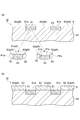
- FIG. 2 is a cross-sectional view showing an example of a plasma processing apparatus that performs the method shown in FIG. 3 includes (a) part and (b) part, and (a) part of FIG. 3 is a cross-sectional view schematically showing the state of the object to be processed before each step of the method shown in FIG.
- FIG. 3B is a cross-sectional view schematically showing the state of the object to be processed after each step of the method shown in FIG.
- FIG. 4 is a diagram showing the execution timing of various processes performed in each step of the method shown in FIG.
- FIG. 5 is a diagram schematically showing a state in which a precoat film is formed on the inner surface of the processing chamber.
- FIG. 6 is a diagram showing the results of Examples obtained for each material of the underlayer.
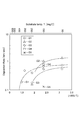
- FIG. 7 shows the results obtained under various process conditions.
- FIG. 1 is a flow diagram illustrating a method of an embodiment.
- a method MT according to an embodiment shown in FIG. 1 is a method for processing an object to be processed (hereinafter also referred to as “wafer”).
- a series of steps can be performed using a single plasma processing apparatus.
- FIG. 2 is a diagram illustrating an example of a plasma processing apparatus.
- FIG. 2 schematically shows a cross-sectional structure of a plasma processing apparatus 10 that can be used in various embodiments of a method for processing an object.
- the plasma processing apparatus 10 is an inductively coupled plasma etching apparatus.
- the plasma processing apparatus 10 includes a processing container 1.
- the processing container 1 is provided airtight.
- the processing container 1 includes a conductive material.
- the inner wall surface of the processing container 1 may include a material such as anodized aluminum.
- the processing container 1 is assembled so as to be disassembled, and is grounded by a ground wire 1a.
- the processing container 1 is partitioned into an antenna chamber 3 and a processing chamber 4 by a dielectric wall 2 in the vertical direction.
- the dielectric wall 2 constitutes the ceiling wall of the processing chamber 4.
- the dielectric wall 2 is made of ceramics such as Al 2 O 3 , quartz, or the like.
- a shower casing 11 for supplying a processing gas is fitted into the lower portion of the dielectric wall 2.
- the shower housing 11 is provided in a cross shape and supports the dielectric wall 2 from below.
- the shower casing 11 that supports the dielectric wall 2 is suspended from the ceiling of the processing container 1 by a plurality of suspenders (not shown).
- the shower housing 11 can include a conductive material such as metal.
- the inner surface of the shower housing 11 may include, for example, anodized aluminum so as not to generate contaminants.
- a gas flow path 12 extending along the dielectric wall 2 is formed in the shower housing 11, and a plurality of gas supply holes 12 a extending toward the susceptor 22 communicate with the gas flow path 12.
- a gas supply pipe 20 a is provided in the center of the upper surface of the dielectric wall 2 so as to communicate with the gas flow path 12.
- the gas supply pipe 20a extends from the dielectric wall 2 to the outside of the processing container 1, and is connected to a processing gas supply system 20 including a processing gas supply source and a valve system. In the plasma processing, the processing gas supplied from the processing gas supply system 20 is supplied into the shower housing 11 through the gas supply pipe 20a, and the lower surface of the shower housing 11 (the surface facing the processing chamber 4).
- the gas supply holes 12a are discharged into the processing chamber 4.
- a support shelf 5 protruding inward is provided between the side wall 3 a of the antenna chamber 3 and the side wall 4 a of the processing chamber 4 in the processing container 1, and the dielectric wall 2 is placed on the support shelf 5. .
- a high frequency antenna 13 is disposed on the dielectric wall 2 so as to face the dielectric wall 2.
- the high frequency antenna 13 is separated from the dielectric wall 2 within a range of, for example, 50 mm or less by a spacer 13a made of an insulating member.
- a spacer 13a made of an insulating member.
- four feeding members 16 extending in a direction perpendicular to the upper surface of the dielectric wall 2 (in the vertical direction) are provided.
- the high frequency power supply 15 is connected.
- the power supply member 16 is disposed around the gas supply pipe 20a.
- high-frequency power for plasma generation with a frequency of, for example, about 13.56 [MHz] for forming an induction electric field is supplied from the high-frequency power supply 15 into the processing chamber 4 via the high-frequency antenna 13.
- the induction electric field is formed in the processing chamber 4, and the induction electric field causes the shower housing 11 to enter the processing chamber 4.
- a plasma of the supplied processing gas is generated.
- casing 11 is provided in the cross shape, and even if the shower housing
- a susceptor 22 (mounting table) is provided below the processing chamber 4 (opposite the dielectric wall 2) so as to face the high-frequency antenna 13 with the dielectric wall 2 interposed therebetween.
- a wafer W that is an object to be processed is placed on the susceptor 22.
- the susceptor 22 can include a conductive material.
- the surface of the susceptor 22 can include, for example, anodized aluminum or alumina sprayed aluminum.
- the wafer W placed on the susceptor 22 is attracted and held on the susceptor 22 by an electrostatic chuck (not shown).
- the susceptor 22 is accommodated in the insulator frame 24 and supported by the support column 25.
- the support column 25 has a hollow structure. Between the insulator frame 24 that houses the susceptor 22 and the bottom of the processing container 1 (the side of the processing container 1 where the support column 25 is provided), a bellows 26 that hermetically surrounds the support column 25 is disposed. Yes.
- a loading / unloading port 27a for loading / unloading the wafer W and a gate valve 27 for opening / closing the loading / unloading port 27a are provided on the side wall 4a of the processing chamber 4.
- the susceptor 22 is connected to a high-frequency power source 29 via a matching unit 28 by a power feeding rod 25 a provided in the support column 25.
- the high frequency power supply 29 applies a bias high frequency power, for example, a bias high frequency power having a frequency of about 400 [kHz] to 6 [MHz] to the susceptor 22 during plasma processing.
- the ions in the plasma generated in the processing chamber 4 can be effectively drawn into the wafer W by the high frequency power for bias.
- a temperature control mechanism including a heating means such as a ceramic heater, a refrigerant flow path, and the like, and a temperature sensor are provided in the susceptor 22 (none of which is shown). Piping and wiring for these mechanisms and members are all led out of the processing vessel 1 through the inside of the support column 25.
- An exhaust device 30 including a vacuum pump or the like is connected to the bottom of the processing chamber 4 (the side of the processing chamber 4 where the support column 25 is provided) via an exhaust pipe 31.
- the processing chamber 4 is evacuated by the exhaust device 30, and the inside of the processing chamber 4 is set and maintained at a predetermined vacuum atmosphere (for example, an atmospheric pressure of about 1.33 [Pa]) during the plasma processing.
- the high frequency antenna 13 has four power feeding units (for example, a power feeding unit 41, a power feeding unit 43, and the like).
- the four power supply units are connected to the power supply member 16.
- the four power feeding units are arranged around the center of the high-frequency antenna 13 so as to be separated by about 90 degrees, for example.
- Two antenna wires extend outward from each of the four power feeding units, and each antenna wire is grounded via a capacitor 18.
- the plasma processing apparatus 10 includes a control unit Cnt.
- the control unit Cnt is a computer including a processor, a storage unit, an input device, a display device, and the like, and controls each unit of the plasma processing apparatus 10.
- the control unit Cnt operates according to a program based on the input recipe and sends out a control signal. According to a control signal from the control unit Cnt, the selection and flow rate of the gas supplied from the processing gas supply system 20, the exhaust of the exhaust device 30, the power supply from the high frequency power supply 15 and the high frequency power supply 29, and the temperature of the susceptor 22 , Can be controlled. Note that each step (steps S1 to S4 shown in FIG. 1) of the method (method MT) for processing an object to be processed disclosed in this specification operates each part of the plasma processing apparatus 10 under the control of the control unit Cnt. Can be implemented.
- Part (a) of FIG. 3 is a cross-sectional view schematically showing the state of the object to be processed before each step of the method MT shown in FIG.
- Part (b) of FIG. 3 is a cross-sectional view schematically showing the state of the object to be processed after each step of the method MT shown in FIG.
- FIG. 4 is a diagram showing the execution timing of various processes performed in each step of the method MT shown in FIG.
- the method MT shown in FIG. 1 includes steps S1 to S4 as main steps of the method MT.
- step S ⁇ b> 1 first step
- the wafer W is accommodated in the processing chamber 4 of the processing container 1 of the plasma processing apparatus 10.
- the surface inside the process chamber 4 used for implementation of process S1 may have the part covered with the precoat film
- FIG. 5 schematically shows a state in which the precoat film PC is formed on the inner surface of the processing chamber 4. Although FIG. 5 shows the precoat film PC formed on the entire inner surface of the processing chamber 4, the precoat film PC may be formed on a part of the inner surface of the processing chamber 4.
- the precoat film PC is a film containing silicon and halogen (for example, fluorine).
- the proportion of silicon can be about one time or less of the proportion of halogen.
- the thickness of the precoat film PC is substantially uniform, but is on average about 50 to 100 [nm] or more.
- the wafer W accommodated in the processing chamber 4 in the step S1 includes a metal part 61 and an insulating part 62, as shown in part (a) of FIG.
- the main surface 6 of the wafer W is formed by performing CMP (Chemical-Mechanical-Polishing or Planarization) after performing damascene, and the metal part 61 is formed through performing damascene.
- the metal part 61 is embedded in the insulating part 62 on the main surface 6, and the surface 61 a (first surface) of the metal part 61 and the surface 62 a (second surface) of the insulating part 62 on the main surface 6 side. Is exposed.
- the surface 61a of the metal part 61 and the surface 62a of the insulating part 62 may both be included in the main surface 6 of the wafer W. Not only the surface 62a of the insulating part 62 but also the surface 62a of the insulating part 62 among the surface 61a of the metal part 61 and the surface 62a of the insulating part 62 as in the embodiment PTb shown in FIG.
- the front surface 61 a of the metal part 61 is included so as to extend along the main surface 6 at a position lowered from the main surface 6 toward the inside of the wafer W, and the recess of the wafer W is formed on the main surface 6. 61b may be defined.
- the material of the metal part 61 may be copper (Cu), for example.
- the material of the metal part 61 may further be cobalt (Co), tungsten (W), aluminum (Al), rubidium (Ru), tantalum (Ta), titanium (Ti), or the like.
- the insulating unit 62 may be an ILD (Inter Level Dielectric).
- the material of the insulating part 62 may be a metal oxide such as SiO x , SiN x , SiC x , SiOC, SiOCH, Al 2 O 3 , where x is a natural number.
- the material of the insulating part 62 may be an organic material.
- step S2 the pressure in the processing chamber 4 is adjusted to the process pressure. Specifically, the pressure in the processing chamber 4 is adjusted by starting the supply of the first gas into the processing chamber 4. As shown in the graph G1 in FIG. 4, in step S2, the supply of the first gas into the processing chamber 4 is started at time T1 (the supply of the first gas is turned from OFF to ON). Graph G1 shows the start timing and end timing of the supply of the first gas into the processing chamber 4 in the method MT. The supply of the first gas into the processing chamber 4 is continued until time T4. Time T4 is a time after time T1.
- the first gas can be a gas containing oxygen.
- the first gas can be O 2 gas.
- step S3 the insulating film 63 is selectively formed only on the surface 62a of the insulating portion 62 in the main surface 6 of the wafer W by using plasma CVD (CVD: Chemical Vapor Deposition).
- CVD Chemical Vapor Deposition
- step S ⁇ b> 3 the second gas and the high frequency power for plasma generation are supplied into the processing chamber 4, and processing for generating plasma in the processing chamber 4 including the gas in the processing chamber 4 including the second gas is started. .
- the plasma generated in step S3 contains deposition species and etching species.
- the proportion of etching species is greater than the proportion of deposition species.
- the proportion of etching species is about 4 to 6 times the proportion of deposition species.
- the second gas may be a gas containing silicon and halogen.
- the deposition species element is silicon
- the etching species element is halogen. is there.
- the second gas can be, for example, a gas containing silicon and fluorine (for example, SiF 4 gas).
- the deposition type element is silicon.
- the etching species element is fluorine.
- step S ⁇ b> 3 the supply of the second gas into the processing chamber 4 and the supply of the high frequency power for plasma generation into the processing chamber 4 are performed at the same timing.
- step S3 the supply of the second gas into the processing chamber 4 and the supply of high-frequency power for plasma generation into the processing chamber 4 are performed at time T2.
- Both start at the same timing the supply of the second gas and the supply of the high frequency power for plasma generation are switched from OFF to ON at the same timing).
- Graph G2 shows the start timing and end timing of the supply of the second gas into the processing chamber 4 in the method MT.
- Graph G3 shows the start timing and end timing of the supply of the high frequency power for plasma generation into the processing chamber 4 in the method MT.
- Time T2 is a time after time T1 and before time T4.
- the supply of the second gas into the processing chamber 4 is continued until time T4.
- the supply of the high frequency power for plasma generation into the processing chamber 4 is continued until time T3.
- Time T3 is a time after time T2 and before time T4.
- the insulating film 63 is formed only on the surface 62a of the insulating part 62 and is not formed on the surface 61a of the metal part 61, as shown in FIG. As described above, the insulating film 63 is selectively formed on the insulating portion 62 in the main surface 6 of the wafer W by the step S3.
- the insulating film 63 includes halogen (X) when the etching species element contained in the plasma generated in step S3 is halogen (X), and may be, for example, a SiO: X film. In particular, when the etching species element is fluorine, the insulating film 63 is a SiO: F film.
- step S4 the generation of plasma in the processing chamber 4 started in step S3 is terminated.
- step S4 after the supply of the high frequency power for plasma generation into the processing chamber 4 is completed, the supply of the first gas into the processing chamber 4, the supply of the second gas into the processing chamber 4, At the same time.
- the supply of the first gas into the processing chamber 4 and the supply of the second gas into the processing chamber 4 are both ended at the same timing (the first gas supply and the first gas supply). The gas supply of 2 is turned off and maintained at the same timing).
- the etching effect of the etching species on the surface 61a of the metal part 61 is insulative in the case where the plasma generated in step S3 contains not only the deposition species but also a relatively large amount of etching species. Therefore, the deposition of the insulating film 63 by the deposition species proceeds on the surface 62a of the insulating portion 62, but the surface 61a of the metal portion 61 has a film effect due to the etching effect of the etching species. It has been found that the phenomenon that deposition is suppressed occurs.
- This phenomenon is considered due to the fact that the difference between the incubation time of the surface 62a of the insulating part 62 and the incubation time of the surface 61a of the metal part 61 is increased by the etching species. That is, when the incubation is long (in this embodiment, the surface of the metal part), since the nucleation at the initial stage of film growth on the surface is slow, the annihilation rate of the nuclei by etching becomes larger than the nucleation rate and the film growth is suppressed. .
- the incubation is short (in this embodiment, the surface of the insulating film)
- nucleation at the initial stage of film growth on the surface is fast, so that the nucleation rate of the nuclei by etching is smaller than the nucleation rate and the film growth is promoted.
- the ratio between the deposition type and the etching type in the plasma for example, by adjusting the gas type that generates the plasma
- the surface 61a of the metal part 61 is insulated from the process without complicating the process.
- the insulating film 63 can be selectively formed only on the surface 62a of the insulating portion 62 on the main surface 6 of the wafer W where the surface 62a of the portion 62 is exposed.
- a film forming site which is the bottom of a trench groove between metal wirings is locally formed by infrared light (Japanese Patent Laid-Open No. 2-9126) or ultraviolet light (Japanese Patent Laid-Open No. 2002-359241).
- the method MT according to the embodiment does not require such complicated two-stage processing, and only one stage of processing needs to be executed. Is improved. Further, in the method MT according to the embodiment, an insulating film is not formed so as to be embedded between the wiring and the protruding portion, but only from the surface 62a of the insulating portion 62 to the main surface 6 of the wafer W.
- the insulating film 63 can be grown and the trench and hole of the insulating film can be formed by leaving the surface 62a of the part 61 and upward from the surface 62a of the metal part 61, it is possible to greatly reduce the process of forming the wiring. It becomes. Further, in the method MT according to the embodiment, the electron transfer is not performed by using the deposition species and the etching species generated by the plasma, and adjusting the ratios thereof, instead of the selective growth of the insulating film simply based on the difference in the base.
- the insulating film 63 can be selectively grown on the insulating portion 62 rather than the surface 62a (metal surface) of the metal portion 61 having the property of being relatively easily performed.
- the insulating film 63 can be selectively formed only on the surface 62a of the insulating portion 62 in the main surface 6 of the wafer W. It becomes. In particular, even when fluorine is used as the etching seed element, the insulating film 63 can be selectively formed only on the surface 62 a of the insulating portion 62 in the main surface 6 of the wafer W. In addition, since the second gas contains silicon and halogen (for example, fluorine), the plasma generated in step S3 may include deposition species and etching species. Even when the material of the metal part 61 is copper, the insulating film 63 can be selectively formed only on the surface 62 a of the insulating part 62.
- step S3 the supply of the second gas and the supply of the high frequency power for plasma generation are performed at the same timing, so that the deposition by the deposition species and the etching by the etching species are suitably performed with a good balance.
- the selective formation of the insulating film 63 is more preferably realized.
- step S4 since the supply of the second gas and the like is completed after the supply of the high frequency power for plasma generation is completed and the generation of the plasma is completed, the film is deposited excessively by the plasma. However, after the film deposition by the plasma is finished and before the supply of the second gas is finished, the etching is continued by the halogen contained in the second gas, so that the excessive deposition is performed. Can be removed.
- the timing of the supply of the second gas and the supply of the high frequency power for plasma generation is preferably the same, but the increase in the concentration of the second gas in the processing chamber 4 may cause a time delay. In such a case, the supply of high-frequency power may be gradually increased. By doing so, deposition by deposition species and etching by etching species can be performed in a well-balanced manner.
- PC the second gas containing silicon and halogen
- the main gas of the wafer W is formed by the second gas and each atom of silicon and halogen separated from the precoat film PC.
- Example 1 Steps S2 and S3 can be performed, for example, under the following conditions.
- the following conditions are conditions when the precoat film PC is not formed on the inner surface of the processing chamber 4.
- -Pressure value in the processing chamber 4 [Pa]: 0.1 to 10 [Pa]
- Processing gas O 2 gas (first gas), SiF 4 gas (second gas)
- a precoat film PC containing silicon and halogen may be formed on the inner surface of the processing chamber 4 used in step S1.
- the film thickness of the precoat film PC is about 100 [nm] or less.
- the precoat film PC is formed on almost the entire surface of the processing chamber 4.
- Steps S2 to S4 are performed using the following process conditions A, with the material of the underlayer being Si, th-Ox (thermal oxide film), SiN, SiCOH, and Cu, as shown in FIGS. 6 and 7.
- the result was obtained.
- FIG. 6 is a diagram showing the results of Examples obtained for each material of the underlayer.
- the horizontal axis in FIG. 6 represents the execution time [sec] of step S3, and the vertical axis in FIG. 6 represents the thickness (Film Thickness) [nm] of the stacked films.
- FIG. 7 shows the results obtained under various process conditions.
- All the results shown in FIG. 6 are the results obtained under the condition that the temperature of the wafer W (underlayer) is 50 [° C.] when the process S3 is performed together with the process condition A.
- a result G1 shown in FIG. 7 is a result obtained under the process condition A while changing the temperature (T [° C.]) of the wafer W (underlayer) in the step S3.
- the result G2 shown in FIG. 7 shows that the gas flow rate [sccm] in the process condition A is changed while changing the temperature (T [° C.]) of the wafer W (underlayer) in step S3.
- the result G4 shown in FIG. 7 shows the value [Pa] of the pressure in the processing chamber 4 in the process condition A while changing the temperature (T [° C.]) of the wafer W (underlayer) in step S3.
- -Pressure value in the processing chamber 4 [Pa]: 1.7 [Pa] This is the result obtained under the following conditions.
- the result G5 shown in FIG. 7 indicates that the frequency value [MHz] and the bias power value [of the high-frequency power source 29 in the process condition A while changing the temperature (T [° C.]) of the wafer W (underlayer) in step S3.
- step S3 when the temperature of the wafer W (underlayer) is in the range of 50 degrees Celsius or more and 450 degrees Celsius or less, The film lamination on the surface of the underlayer of the material (Cu) is suppressed, and the film lamination on the surface of the underlayer of the insulating material (Si, th-Ox (thermal oxide film), SiN, SiCOH) is promoted. It was found that.
- the material of the underlayer is an insulating material (Si, th-Ox (thermal oxide film), SiN, SiCOH), as the execution time of step S3 increases, The formed film thickness also increases.
- the material of the underlayer is a metallic material (Cu), a film is hardly formed on the underlayer regardless of the execution time of step S3.
- the wafer W (underlayer) in step S3 is used regardless of whether the material of the underlayer is an insulating material (Si, th-Ox (thermal oxide film), SiN, SiCOH). Is not more than 450 degrees Celsius, and more than room temperature (more specifically, 50 degrees Celsius) (that is, within the range of 50 degrees Celsius and 450 degrees Celsius), the process conditions Even if each element included, that is, the pressure in the processing chamber 4, the gas flow rate, the bias power of the high-frequency power source 29, etc. has various values, the lamination rate of the film formed on the underlying layer [nm / sec] is a sufficiently large value. According to the results G1 to G5 shown in FIG.
- the film is formed by Si, th-Ox (thermal oxide film). , SiN, SiCOH, etc., it is suitable when performed on an underlayer of an insulating material.
- step S3 supply of the second gas into the processing chamber 4 and supply of high-frequency power for plasma generation into the processing chamber 4 are performed at time T2, but the second gas into the processing chamber 4 is supplied at time T2.
- the gas supply timing may be earlier than the plasma generation high-frequency power supply timing into the processing chamber 4 to the extent that the plasma state in the processing chamber 4 does not become unstable.
- SYMBOLS 1 Processing container, 10 ... Plasma processing apparatus, 11 ... Shower housing
Landscapes
- Chemical & Material Sciences (AREA)
- Engineering & Computer Science (AREA)
- Plasma & Fusion (AREA)
- Physics & Mathematics (AREA)
- Metallurgy (AREA)
- Organic Chemistry (AREA)
- Materials Engineering (AREA)
- Mechanical Engineering (AREA)
- General Chemical & Material Sciences (AREA)
- Chemical Kinetics & Catalysis (AREA)
- Analytical Chemistry (AREA)
- Inorganic Chemistry (AREA)
- Chemical Vapour Deposition (AREA)
- Plasma Technology (AREA)
- Formation Of Insulating Films (AREA)
- Drying Of Semiconductors (AREA)
Abstract
Description
従って、プラズマ中のデポジション種とエッチング種との割合を調整することで(例えばプラズマを生成するガス種を調整することで)、プロセスを複雑化することなく、金属部61の表面61aと絶縁部62の表面62aとが共に露出しているウエハWの主面6面において、絶縁部62の表面62aにのみ選択的に絶縁膜63を形成することが可能となる。
工程S2,S3は、例えば以下の条件で実施され得る。なお、以下の条件は、処理室4の内側の表面にプリコート膜PCが形成されていない場合の条件である。
・処理室4内の圧力の値[Pa]:0.1~10[Pa]
・高周波電源15の周波数の値[MHz]および高周波電力の値[ワット]:13.56[MHz]、100~5000[ワット]
・高周波電源29の周波数の値[MHz]およびバイアス電力の値[ワット]:0.4~6[MHz]、0~500[ワット]
・処理ガス:O2ガス(第1のガス)、SiF4ガス(第2のガス)
工程S1で用いられる処理室4の内側の表面には、シリコンとハロゲンとを含有するプリコート膜PCが形成されている場合がある。プリコート膜PCの膜厚は約100[nm]以下である。またプリコート膜PCの形成場所は処理室4内のほぼ全面である。
下地層の材料を、Si,th-Ox(熱酸化膜),SiN,SiCOH,Cuのそれぞれとして、下記のプロセス条件Aを用いて工程S2~工程S4を実行し、図6および図7に示す結果を得た。図6は、下地層の材料毎に得られた実施例の結果を示す図である。図6の横軸は、工程S3の実行時間[sec]を表し、図6の縦軸は、積層された膜の厚み(Film Thickness)[nm]を表している。図7は、種々のプロセス条件の下で得られた結果を示す図である。図7の上側の横軸は、工程S3の実行時におけるウエハW(下地層)の温度[℃](T[℃])を表し、図7の下側の横軸は、T[℃]の逆数を1000倍した値(1000/T)を表し、図7の縦軸は、膜の積層率(Deposition Rate)[nm/sec]を表している。
・処理室4内の圧力の値[Pa]:1.33[Pa]
・高周波電源15の周波数の値[MHz]および高周波電力の値[ワット]:13.56[MHz]、2000[ワット]
・高周波電源29の周波数の値[MHz]およびバイアス電力の値[ワット]:2[MHz](4~6[MHz]の範囲内で可変)、0[ワット](0~600[ワット]の範囲内で可変)
・処理ガス:O2ガス(第1のガス)、SiF4ガス(第2のガス)
・ガス流量[sccm]:(O2ガス)200[sccm]、(SiF4ガス)7.5[sccm]
・ガス流量[sccm]:(O2ガス)100[sccm]、(SiF4ガス)7.5[sccm]
とした条件の下で得られた結果である。図7に示す結果G3は、工程S3におけるウエハW(下地層)の温度(T[℃])を変化させつつ、プロセス条件Aのうち処理室4内の圧力の値[Pa]を、
・処理室4内の圧力の値[Pa]:13[Pa]
とした条件の下で得られた結果である。
・処理室4内の圧力の値[Pa]:1.7[Pa]
とした条件の下で得られた結果である。図7に示す結果G5は、工程S3におけるウエハW(下地層)の温度(T[℃])を変化させつつ、プロセス条件Aのうち高周波電源29の周波数の値[MHz]およびバイアス電力値[ワット]を、
・高周波電源29の周波数の値[MHz]およびバイアス電力の値[ワット]:2[MHz](4~6[MHz]の範囲内で可変)、0[ワット](0~600[ワット]の範囲内で可変)
とした条件の下で得られた結果である。図7に示す結果G1~G5は、下地層の材料がSi,th-Ox(熱酸化膜),SiN,SiCOHの何れであっても、同様に得られた。
Claims (9)
- 被処理体を処理する方法であって、該被処理体は、金属部および絶縁部と、主面と、を含み、該主面の側において該金属部の第1の表面と該絶縁部の第2の表面とが露出されており、該方法は、
プラズマ処理装置の処理室内に前記被処理体を収容する第1工程と、
前記第1工程の後に、前記処理室内に第1のガスの供給を開始する第2工程と、
前記第2工程の後に、第2のガスとプラズマ生成用高周波電力とを前記処理室内に供給して該第2のガスを含む該処理室内のガスによるプラズマを該処理室内において生成する処理を開始する第3工程と、
を備え、
前記第1のガスは、酸素を含有し、
前記第3工程で生成されるプラズマは、デポジション種とエッチング種とを含有し、
前記第3工程で生成されるプラズマにおいて、前記エッチング種が占める割合は、前記デポジション種が占める割合よりも多い、
方法。 - 前記デポジション種の元素はシリコンであり、前記エッチング種の元素はハロゲンである、
請求項1に記載の方法。 - 前記エッチング種の元素は、フッ素である、
請求項1または請求項2に記載の方法。 - 前記第2のガスは、シリコンとハロゲンとを含有する、
請求項1~3の何れか一項に記載の方法。 - 前記金属部は、銅を含有する、
請求項1~4の何れか一項に記載の方法。 - 前記第3工程は、前記処理室内への前記第2のガスの供給と、該処理室内への前記プラズマ生成用高周波電力の供給とを同じタイミングで行う、
請求項1~5の何れか一項に記載の方法。 - 前記第3工程の後に、プラズマの生成を終了する第4工程をさらに備え、該第4工程は、
前記処理室内への前記プラズマ生成用高周波電力の供給を終了した後に、該処理室内への前記第1のガスの供給と、該処理室内への前記第2のガスの供給と、を同じタイミングで終了する、
請求項6に記載の方法。 - 前記第1工程において、前記処理室の内側の表面は、シリコンとハロゲンとを含有するプリコート膜で覆われている部分を有する、
請求項1~7の何れか一項に記載の方法。 - 前記第3工程において、前記被処理体の温度は、摂氏50度以上且つ摂氏450度以下の範囲内にある、
請求項1~8の何れか一項に記載の方法。
Priority Applications (4)
| Application Number | Priority Date | Filing Date | Title |
|---|---|---|---|
| KR1020197001251A KR102436210B1 (ko) | 2016-06-20 | 2017-06-15 | 피처리체를 처리하는 방법 |
| US16/310,459 US10937660B2 (en) | 2016-06-20 | 2017-06-15 | Method for processing workpiece |
| JP2018523999A JP6722760B2 (ja) | 2016-06-20 | 2017-06-15 | 被処理体を処理する方法 |
| CN201780037999.9A CN109314059B (zh) | 2016-06-20 | 2017-06-15 | 被处理体的处理方法 |
Applications Claiming Priority (2)
| Application Number | Priority Date | Filing Date | Title |
|---|---|---|---|
| JP2016121820 | 2016-06-20 | ||
| JP2016-121820 | 2016-06-20 |
Publications (1)
| Publication Number | Publication Date |
|---|---|
| WO2017221807A1 true WO2017221807A1 (ja) | 2017-12-28 |
Family
ID=60783496
Family Applications (1)
| Application Number | Title | Priority Date | Filing Date |
|---|---|---|---|
| PCT/JP2017/022155 Ceased WO2017221807A1 (ja) | 2016-06-20 | 2017-06-15 | 被処理体を処理する方法 |
Country Status (5)
| Country | Link |
|---|---|
| US (1) | US10937660B2 (ja) |
| JP (1) | JP6722760B2 (ja) |
| KR (1) | KR102436210B1 (ja) |
| CN (1) | CN109314059B (ja) |
| WO (1) | WO2017221807A1 (ja) |
Families Citing this family (1)
| Publication number | Priority date | Publication date | Assignee | Title |
|---|---|---|---|---|
| US11887814B2 (en) * | 2020-02-10 | 2024-01-30 | Hitachi High-Tech Corporation | Plasma processing method |
Citations (5)
| Publication number | Priority date | Publication date | Assignee | Title |
|---|---|---|---|---|
| JPS61251040A (ja) * | 1985-04-27 | 1986-11-08 | Fujitsu Ltd | 酸化膜の選択成長方法 |
| JPS6410650A (en) * | 1987-07-03 | 1989-01-13 | Fujitsu Ltd | Forming method for interlayer insulating layer |
| JPH07288254A (ja) * | 1994-04-19 | 1995-10-31 | Mitsubishi Electric Corp | 半導体装置およびその製造方法 |
| JP2006332538A (ja) * | 2005-05-30 | 2006-12-07 | Fujitsu Ltd | 半導体装置の製造方法 |
| JP2013219198A (ja) * | 2012-04-09 | 2013-10-24 | Nissin Electric Co Ltd | 薄膜製造方法 |
Family Cites Families (20)
| Publication number | Priority date | Publication date | Assignee | Title |
|---|---|---|---|---|
| JPH029126A (ja) | 1988-06-28 | 1990-01-12 | Anelva Corp | 薄膜形成方法 |
| JP2629579B2 (ja) * | 1993-10-14 | 1997-07-09 | 日本電気株式会社 | 半導体装置の製造方法及び製造装置 |
| JPH07226437A (ja) | 1994-02-10 | 1995-08-22 | Mitsubishi Electric Corp | 半導体装置及びその製造方法 |
| US5596431A (en) * | 1995-03-29 | 1997-01-21 | Philips Electronics North America Corp. | Plasma addressed liquid crystal display with etched electrodes |
| US6107192A (en) * | 1997-12-30 | 2000-08-22 | Applied Materials, Inc. | Reactive preclean prior to metallization for sub-quarter micron application |
| JP3694470B2 (ja) | 2001-05-31 | 2005-09-14 | 沖電気工業株式会社 | 半導体装置の製造方法 |
| US7250373B2 (en) * | 2004-08-27 | 2007-07-31 | Applied Materials, Inc. | Method and apparatus for etching material layers with high uniformity of a lateral etch rate across a substrate |
| DE102005004360A1 (de) * | 2005-01-31 | 2006-08-17 | Advanced Micro Devices, Inc., Sunnyvale | Effizientes Verfahren zum Herstellen und Zusammenfügen eines mikroelektronischen Chips mit Lothöckern |
| DE102005035772A1 (de) * | 2005-07-29 | 2007-02-01 | Advanced Micro Devices, Inc., Sunnyvale | Technik zum effizienten Strukturieren einer Höckerunterseitenmetallisierungsschicht unter Anwendung eines Trockenätzprozesses |
| JP2007194284A (ja) * | 2006-01-17 | 2007-08-02 | Tokyo Electron Ltd | プラズマ処理方法、プラズマ処理装置、及び記憶媒体 |
| US7932181B2 (en) * | 2006-06-20 | 2011-04-26 | Lam Research Corporation | Edge gas injection for critical dimension uniformity improvement |
| JP5710267B2 (ja) * | 2007-12-21 | 2015-04-30 | ラム リサーチ コーポレーションLam Research Corporation | シリコン構造体の製造及びプロファイル制御を伴うシリコンディープエッチング |
| US7749789B2 (en) * | 2008-03-18 | 2010-07-06 | Solid-State Research, Inc. | CMOS-compatible bulk-micromachining process for single-crystal MEMS/NEMS devices |
| US20110207323A1 (en) * | 2010-02-25 | 2011-08-25 | Robert Ditizio | Method of forming and patterning conformal insulation layer in vias and etched structures |
| US9036956B2 (en) * | 2012-02-17 | 2015-05-19 | Haynes and Boone, LLP | Method of fabricating a polymer waveguide |
| FR3000602B1 (fr) * | 2012-12-28 | 2016-06-24 | Commissariat A L Energie Atomique Et Aux Energies Alternatives | Procede de gravure d'un materiau dielectrique poreux |
| US8987139B2 (en) * | 2013-01-29 | 2015-03-24 | Applied Materials, Inc. | Method of patterning a low-k dielectric film |
| US9236292B2 (en) * | 2013-12-18 | 2016-01-12 | Intel Corporation | Selective area deposition of metal films by atomic layer deposition (ALD) and chemical vapor deposition (CVD) |
| US9515166B2 (en) * | 2014-04-10 | 2016-12-06 | Applied Materials, Inc. | Selective atomic layer deposition process utilizing patterned self assembled monolayers for 3D structure semiconductor applications |
| US9633902B2 (en) * | 2015-03-10 | 2017-04-25 | Kabushiki Kaisha Toshiba | Method for manufacturing semiconductor device that includes dividing semiconductor substrate by dry etching |
-
2017
- 2017-06-15 KR KR1020197001251A patent/KR102436210B1/ko active Active
- 2017-06-15 CN CN201780037999.9A patent/CN109314059B/zh active Active
- 2017-06-15 WO PCT/JP2017/022155 patent/WO2017221807A1/ja not_active Ceased
- 2017-06-15 US US16/310,459 patent/US10937660B2/en active Active
- 2017-06-15 JP JP2018523999A patent/JP6722760B2/ja active Active
Patent Citations (5)
| Publication number | Priority date | Publication date | Assignee | Title |
|---|---|---|---|---|
| JPS61251040A (ja) * | 1985-04-27 | 1986-11-08 | Fujitsu Ltd | 酸化膜の選択成長方法 |
| JPS6410650A (en) * | 1987-07-03 | 1989-01-13 | Fujitsu Ltd | Forming method for interlayer insulating layer |
| JPH07288254A (ja) * | 1994-04-19 | 1995-10-31 | Mitsubishi Electric Corp | 半導体装置およびその製造方法 |
| JP2006332538A (ja) * | 2005-05-30 | 2006-12-07 | Fujitsu Ltd | 半導体装置の製造方法 |
| JP2013219198A (ja) * | 2012-04-09 | 2013-10-24 | Nissin Electric Co Ltd | 薄膜製造方法 |
Also Published As
| Publication number | Publication date |
|---|---|
| US20190326124A1 (en) | 2019-10-24 |
| CN109314059A (zh) | 2019-02-05 |
| CN109314059B (zh) | 2023-06-23 |
| JPWO2017221807A1 (ja) | 2019-03-28 |
| KR102436210B1 (ko) | 2022-08-26 |
| US10937660B2 (en) | 2021-03-02 |
| JP6722760B2 (ja) | 2020-07-15 |
| KR20190019153A (ko) | 2019-02-26 |
Similar Documents
| Publication | Publication Date | Title |
|---|---|---|
| TWI760555B (zh) | 蝕刻方法 | |
| KR102426264B1 (ko) | 에칭 방법 | |
| TWI775819B (zh) | 蝕刻方法 | |
| TWI704635B (zh) | 增進製程均勻性的方法及系統 | |
| KR102363052B1 (ko) | 피처리체를 처리하는 방법 | |
| TWI691612B (zh) | 矽化鎳奈米線的直接沉積 | |
| KR102257855B1 (ko) | 피에칭층을 에칭하는 방법 | |
| CN104641455A (zh) | 自由基成分的氧化物蚀刻 | |
| JP2016512395A5 (ja) | ||
| TW202025212A (zh) | 低溫高品質的介電膜 | |
| KR20210097045A (ko) | 에칭 방법, 기판 처리 장치, 및 기판 처리 시스템 | |
| JP6606609B2 (ja) | 被処理体を処理する方法 | |
| US9305795B2 (en) | Plasma processing method | |
| JP6722760B2 (ja) | 被処理体を処理する方法 | |
| KR20210097044A (ko) | 에칭 방법, 기판 처리 장치, 및 기판 처리 시스템 | |
| US20150140233A1 (en) | Methods for preferential growth of cobalt within substrate features | |
| TWI757442B (zh) | 成膜方法 | |
| US10283370B1 (en) | Silicon addition for silicon nitride etching selectivity |
Legal Events
| Date | Code | Title | Description |
|---|---|---|---|
| ENP | Entry into the national phase |
Ref document number: 2018523999 Country of ref document: JP Kind code of ref document: A |
|
| 121 | Ep: the epo has been informed by wipo that ep was designated in this application |
Ref document number: 17815275 Country of ref document: EP Kind code of ref document: A1 |
|
| NENP | Non-entry into the national phase |
Ref country code: DE |
|
| ENP | Entry into the national phase |
Ref document number: 20197001251 Country of ref document: KR Kind code of ref document: A |
|
| 122 | Ep: pct application non-entry in european phase |
Ref document number: 17815275 Country of ref document: EP Kind code of ref document: A1 |