WO2017221601A1 - モジュール及びその製造方法 - Google Patents
モジュール及びその製造方法 Download PDFInfo
- Publication number
- WO2017221601A1 WO2017221601A1 PCT/JP2017/018865 JP2017018865W WO2017221601A1 WO 2017221601 A1 WO2017221601 A1 WO 2017221601A1 JP 2017018865 W JP2017018865 W JP 2017018865W WO 2017221601 A1 WO2017221601 A1 WO 2017221601A1
- Authority
- WO
- WIPO (PCT)
- Prior art keywords
- substrate
- opening
- lead frames
- resist
- adhesive
- Prior art date
- Legal status (The legal status is an assumption and is not a legal conclusion. Google has not performed a legal analysis and makes no representation as to the accuracy of the status listed.)
- Ceased
Links
Images



Classifications
-
- G—PHYSICS
- G01—MEASURING; TESTING
- G01F—MEASURING VOLUME, VOLUME FLOW, MASS FLOW OR LIQUID LEVEL; METERING BY VOLUME
- G01F1/00—Measuring the volume flow or mass flow of fluid or fluent solid material wherein the fluid passes through a meter in a continuous flow
- G01F1/68—Measuring the volume flow or mass flow of fluid or fluent solid material wherein the fluid passes through a meter in a continuous flow by using thermal effects
- G01F1/684—Structural arrangements; Mounting of elements, e.g. in relation to fluid flow
-
- H—ELECTRICITY
- H10—SEMICONDUCTOR DEVICES; ELECTRIC SOLID-STATE DEVICES NOT OTHERWISE PROVIDED FOR
- H10W—GENERIC PACKAGES, INTERCONNECTIONS, CONNECTORS OR OTHER CONSTRUCTIONAL DETAILS OF DEVICES COVERED BY CLASS H10
- H10W72/00—Interconnections or connectors in packages
-
- H—ELECTRICITY
- H10—SEMICONDUCTOR DEVICES; ELECTRIC SOLID-STATE DEVICES NOT OTHERWISE PROVIDED FOR
- H10W—GENERIC PACKAGES, INTERCONNECTIONS, CONNECTORS OR OTHER CONSTRUCTIONAL DETAILS OF DEVICES COVERED BY CLASS H10
- H10W74/00—Encapsulations, e.g. protective coatings
-
- H—ELECTRICITY
- H10—SEMICONDUCTOR DEVICES; ELECTRIC SOLID-STATE DEVICES NOT OTHERWISE PROVIDED FOR
- H10W—GENERIC PACKAGES, INTERCONNECTIONS, CONNECTORS OR OTHER CONSTRUCTIONAL DETAILS OF DEVICES COVERED BY CLASS H10
- H10W74/00—Encapsulations, e.g. protective coatings
- H10W74/01—Manufacture or treatment
-
- H—ELECTRICITY
- H10—SEMICONDUCTOR DEVICES; ELECTRIC SOLID-STATE DEVICES NOT OTHERWISE PROVIDED FOR
- H10W—GENERIC PACKAGES, INTERCONNECTIONS, CONNECTORS OR OTHER CONSTRUCTIONAL DETAILS OF DEVICES COVERED BY CLASS H10
- H10W72/00—Interconnections or connectors in packages
- H10W72/50—Bond wires
- H10W72/541—Dispositions of bond wires
- H10W72/5449—Dispositions of bond wires not being orthogonal to a side surface of the chip, e.g. fan-out arrangements
Definitions
- the present invention relates to a module and a manufacturing method thereof.
- a semiconductor sensor element having a measurement region including a resistance temperature detector and a heating resistor formed on a cavity provided in a semiconductor substrate, and heating the heating resistor so as to be higher than the temperature of the resistance temperature detector by a predetermined temperature
- a thermal air flow sensor that includes a control circuit that performs control to flow current and obtains an air flow signal representing an air flow rate, and a terminal material that outputs the air flow signal to the outside (for example, Patent Documents). 1).
- the control circuit of the thermal air flow sensor includes an insulating substrate and electric parts such as a semiconductor chip and a chip capacitor arranged on the insulating substrate.
- the terminal material described above has an end integrated with the insulating substrate.
- the control circuit is electrically connected to the terminal material through a wire.
- a part of the semiconductor sensor element, a control circuit, a wire, and a part of the terminal material are integrally covered with a molding material.
- the objective of this invention is providing the module which suppresses peeling of an adhesive agent, and its manufacturing method.
- a module includes a base on which an electronic circuit is formed, a plurality of lead frames electrically connected to the electronic circuit, a resist formed on at least one of the front and back surfaces of the base, and the base An opening formed in the resist so as to be exposed, an adhesive filling the opening and bonding the substrate and the plurality of lead frames, a part of the plurality of lead frames, and a sealing body for sealing the substrate Have.
- the present invention it is possible to provide a module that suppresses peeling of the adhesive and a method for manufacturing the module.
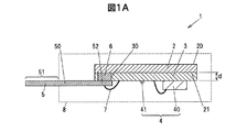
- FIG. 1A is a cross-sectional view illustrating a module according to an embodiment.
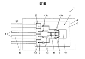
- FIG. 1B is a bottom view showing the back surface of the module.
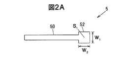
- FIG. 2A is a plan view showing a lead frame of the module according to the embodiment.
- FIG. 2B is a bottom view showing the opening formed in the resist.
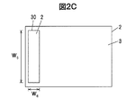
- FIG. 2C is a bottom view showing an opening according to a modification.
- FIG. 3A is a cross-sectional view illustrating the module manufacturing method according to the embodiment.
- FIG. 3B is a cross-sectional view illustrating the module manufacturing method according to the embodiment.
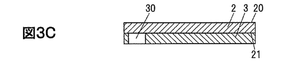
- FIG. 3C is a cross-sectional view illustrating the module manufacturing method according to the embodiment.
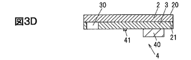
- FIG. 3D is a cross-sectional view illustrating the module manufacturing method according to the embodiment.
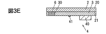
- FIG. 3E is a cross-sectional view illustrating the module manufacturing method according to the embodiment.
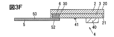
- FIG. 3F is a cross-sectional view illustrating the module manufacturing method according to the embodiment.
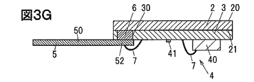
- FIG. 3G is a cross-sectional view illustrating the module manufacturing method according to the embodiment.
- the module according to the embodiment exposes a base body on which an electronic circuit is formed, a plurality of lead frames electrically connected to the electronic circuit, a resist formed on at least one of the front surface and the back surface of the base body, and the base body.
- a resist formed on at least one of the front surface and the back surface of the base body, and the base body.
- a base having a pattern corresponding to an electronic circuit is prepared on at least one of the front and back surfaces, a resist corresponding to the pattern is formed on the surface on which the pattern is formed, and the base is exposed.
- Forming an electronic circuit on the base filling the opening with an adhesive, and joining the base and the ends of the plurality of lead frames via the adhesive to electrically connect the electronic circuit and the plurality of lead frames.
- a part of the plurality of lead frames and the base are sealed with a sealing resin to form a sealing body.
- the adhesive is filled in the opening formed in the resist, the adhesive is thicker than the case where the adhesive is directly applied to the substrate or the resist. Peeling can be suppressed.
- FIG. 1A is a cross-sectional view showing a module according to the embodiment, and FIG. 1B is a bottom view showing a back surface of the module.
- 2A is a plan view showing a lead frame of the module according to the embodiment
- FIG. 2B is a bottom view showing openings formed in the resist
- FIG. 2C is a bottom view showing openings according to a modification. is there.
- a dotted line outside FIGS. 1A and 1B indicates the sealing body 8.
- 2B and 2C, the wiring pattern 43 and the like of the electronic circuit 4 are not shown.
- the ratio between figures may be different from the actual ratio.
- the module 1 includes a substrate 2 as a base on which an electronic circuit 4 is formed, a plurality of lead frames 5 electrically connected to the electronic circuit 4, a surface 20 of the substrate 2, and A resist 3 formed on at least one of the back surfaces 21, an opening 30 formed in the resist 3 so that the substrate 2 is exposed, and an adhesive that fills the opening 30 and joins the substrate 2 and the plurality of lead frames 5. 6, a part of the plurality of lead frames 5, and a sealing body 8 that seals the substrate 2.
- the electronic circuit 4 according to the present embodiment is formed with the lead frame 5 on the back surface 21 side of the substrate 2 as an example, but is not limited to this. They may be formed on the front surface 20 and the back surface 21.
- the module 1 is formed, for example, by transfer molding for sealing the substrate 2 or the like with a sealing resin.
- the integrated lead frame 5 and substrate 2 are set in a mold cavity heated to approximately 180 ° C.
- a thermosetting resin tablet used as a sealing resin is put into a pot adjacent to the cavity. The tablet starts to melt in the pot, and when the pressure is applied to the pot, the tablet is fed into the cavity through a gate connecting the pot and the cavity.
- the liquid tablet is filled in the cavity and cured to form the sealing body 8.
- the module 1 formed in this way has a difference in deformation amount of the substrate 2 or the like due to a temperature change in the process of being taken out of the mold and cooled, and stress is generated inside.
- the difference in the deformation amount is caused by a difference in linear expansion coefficient between the sealing resin, the substrate 2, the resist 3, the lead frame 5, the adhesive 6, and the like.
- the sealing body 8 contracts with different linear expansion coefficients at the glass transition temperature (Tg) until it is taken out from the mold and reaches room temperature, that is, from the filling temperature to room temperature.
- the sealing body 8, the substrate 2, the resist 3, the lead frame 5, the adhesive 6 and the like shrink with different linear expansion coefficients from the filling temperature to room temperature, for example, stress that warps the substrate 2 is generated. Arise.
- the thickness is thin (approximately 18 ⁇ m as an example), and thus the adhesive is peeled off from the resist and the wire is disconnected. The problem occurs.
- the module 1 of this embodiment does not directly apply the adhesive 6 to the resist 3 but provides an opening 30 in the resist 3 so that the thickness of the adhesive 6 is increased.
- the adhesive 6 is thickened (as an example, approximately 30 ⁇ m), and peeling of the adhesive 6 is suppressed.
- the substrate 2 has a plate shape. As shown in FIG. 1B, the substrate 2 has a resist 3 formed on the back surface 21.
- substrate 2 of this embodiment is a glass epoxy board
- An electronic circuit 4 is formed on the back surface 21 of the substrate 2.
- a plurality of wiring patterns 43 are formed on the substrate 2.
- the wiring pattern 43 is formed by copper plating.
- the pad 43 a that is one end of the wiring pattern 43 is electrically connected to a sensor IC (Integrated Circuit) 40 via a wire 7.
- the pad 43 b which is the other end of the wiring pattern 43 is electrically connected to the lead frame 5 through the wire 7.
- the wire 7 is a thin wire such as gold, aluminum, or copper.
- the resist 3 is a covering material for protecting a specific area.
- This resist 3 may be formed by, for example, a printing method or a photolithography method.
- the thickness of the resist 3 is approximately 30 ⁇ m as an example.
- a plurality of openings 30 through which the back surface 21 of the substrate 2 is exposed are formed side by side.
- the opening 30 is formed for each of the plurality of lead frames 5.
- the opening 30 has a rectangular shape in which one width is W 3 and the other width is W 4 .
- the width W 3 is set to be equal to or smaller than the width W 1 of the end portion 52 of the lead frame 5.
- the width W 4 is, for example, to a width W 2 of the end portion 52 below. That is, the area S 2 of the opening 30 has an area equal to or smaller than the area S 1 of the end portion 52 of the lead frame 5 in order to suppress the outflow of the adhesive 6.
- the width W 3 of this embodiment is equal to the width W 4 .
- the opening 30 may be one large opening as shown in FIG. 2C, for example.
- the width W 5 in the longitudinal direction of the opening 30 is longer than the sum of the widths W 1 of the end portions 52 of the lead frame 5 because the plurality of lead frames 5 are arranged at intervals while maintaining insulation.
- the width W 6 of the opening 30 is equal to or smaller than the width W 2 of the end portion 52 of the lead frame 5 similarly to the width W 4 .
- the electronic circuit 4 includes a sensor IC 40 and an electronic component 41, and is electrically connected via a wiring pattern 43 and wires 7.
- the illustrated electronic circuit 4 is an example and is not limited thereto.
- the sensor IC 40 is a semiconductor element including a sensor that converts a detected physical quantity into an electrical quantity, an amplifier that amplifies an output signal of the sensor, and the like.
- the electronic component 41 is, for example, a resistor or a capacitor.
- the lead frame 5 is formed in an elongated plate shape by, for example, punching or etching.
- the lead frame 5 is formed using, for example, a conductive metal material such as aluminum or copper, or an alloy material such as brass.
- the lead frame 5 has a base portion 50 and an end portion 52.
- the base portion 50 has an elongated shape, and a tip portion projects from one surface of the sealing body 8.
- the protruding base portion 50 becomes a terminal portion 51 to be inserted into the female terminal of the connector to which the module 1 is connected.
- the end portion 52 is formed at the end portion of the base portion 50, for example.
- the end portion 52 has a width (W 1 ) wider than the width of the base portion 50 and has a rectangular shape.
- W 1 width
- W 2 width
- the wire 7 is joined to the end portion 52, and the lead frame 5 and the wiring pattern 43 are electrically connected.
- the adhesive 6 is an insulating adhesive containing silicon dioxide, magnesium oxide, aluminum oxide, or the like.
- the adhesive 6 is filled in the opening 30 and joins the substrate 2 and the lead frame 5.
- the thickness of the adhesive 6 is substantially the same as the thickness d of the resist 3.
- the substrate 2 and the lead frame 5 are integrated with the end 52 in contact with the resist 3, but the end 52 is not in contact with the resist 3 or the end 52 is within an allowable range.
- a part of the adhesive 6 may be interposed between the resist 3 and the resist 3.
- sealing body 8 covers and integrally covers the substrate 2, the electronic circuit 4, and one end of the lead frame 5 by transfer molding.
- the sealing body 8 is obtained by curing a thermosetting molding material in which a PPS (Poly Phenylene Sulfide) resin or an epoxy resin is a main component and a silica (silicon dioxide) filler is added.
- an epoxy resin is used as the thermosetting molding material.
- the sealing body 8 mainly protects the sensor IC 40 and the like from environments such as light, heat, and humidity.
- 3A to 3G are cross-sectional views illustrating a module manufacturing method according to the embodiment.
- the method for manufacturing the module 1 mainly includes preparing a substrate 2 having a pattern corresponding to the electronic circuit 4 on the back surface 21, forming a resist 3 corresponding to the pattern on the back surface 21 having the pattern formed thereon, and the substrate 2. Is formed, an electronic circuit 4 is formed on the substrate 2, the opening 30 is filled with the adhesive 6, and the substrate 2 and the end portions 52 of the plurality of lead frames 5 are joined via the adhesive 6. Then, the electronic circuit 4 and the plurality of lead frames 5 are electrically connected, and a part of the plurality of lead frames 5 and the substrate 2 are sealed with a sealing resin to form the sealing body 8. .
- a substrate 2 having a pattern corresponding to the electronic circuit 4 formed on the back surface 21 is prepared.
- This pattern is, for example, a pattern in which the wiring pattern 43 and the sensor IC 40 shown in FIG. 1B are arranged.
- a resist 3 is applied to the back surface 21.
- the applied resist 3 is etched based on the etching method, and the resist 3 corresponding to the wiring pattern 43 and the like is formed on the back surface 21 on which the wiring pattern 43 and the like are formed.
- An exposed opening 30 is formed.
- the sensor IC 40 and the electronic component 41 constituting the electronic circuit 4 are arranged on the substrate 2.
- the opening 6 is filled with the adhesive 6.
- the substrate 2 and the end portions 52 of the plurality of lead frames 5 are bonded together with an adhesive 6.
- the electronic circuit 4 and the plurality of lead frames 5 are electrically connected.
- This connection is performed, for example, by connecting the sensor IC 40 and the pad 43a and the pad 43b and the lead frame 5 with the wire 7 based on the wire bonding method.
- the substrate 2 shown in FIG. 3G is set in a mold heated to the filling temperature.
- a part of the plurality of lead frames 5 and the substrate 2 are subjected to transfer molding with a sealing resin to form a sealing body 8 to obtain a module 1 shown in FIG. 1A.
- the thickness of the adhesive 6 is less than that in the case where the adhesive is directly applied to the substrate or the resist.
- the thickness d becomes substantially the same as the thickness d of 3 and the peeling of the adhesive 6 can be suppressed.
- the module 1 can form the opening 30 in the process of forming the wiring pattern 43 and the like by etching, the manufacturing cost can be suppressed as compared with the case of forming in the separate process.
- the module 1 Since the module 1 has a thickness of the adhesive 6, it becomes easy to relieve stress. Therefore, durability against stress is improved as compared with a case where the module 1 is directly applied to a substrate or a resist.
- the module 1 since the adhesive 6 is filled in the opening 30 and the area S 2 of the opening 30 is equal to or less than the area S 1 of the end 52, the adhesive 6 is surrounded by the substrate 2, the resist 3, and the end 52. Thus, it becomes difficult to flow out of the opening 30. Therefore, the module 1 suppresses the contamination of the terminal portion 51 due to the outflow of the adhesive 6 from the opening 30, and the reliability as the connector terminal is improved.
- Module 2 Substrate 3 Resist 4 Electronic Circuit 5 Lead Frame 6 Adhesive 8 Sealing Body 30 Opening 50 Base 52 End
Landscapes
- Physics & Mathematics (AREA)
- Fluid Mechanics (AREA)
- General Physics & Mathematics (AREA)
- Structures Or Materials For Encapsulating Or Coating Semiconductor Devices Or Solid State Devices (AREA)
- Measuring Volume Flow (AREA)
- Encapsulation Of And Coatings For Semiconductor Or Solid State Devices (AREA)
- Lead Frames For Integrated Circuits (AREA)
Abstract
モジュール1は、電子回路4が形成された基板2と、電子回路4と電気的に接続された複数のリードフレーム5と、基板2の表面20及び裏面21の少なくとも一方に形成されたレジスト3と、基板2が露出するようにレジスト3に形成された開口30と、開口30に充填され、基板2と複数のリードフレーム5とを接合する接着剤6と、複数のリードフレーム5の一部、及び基板2を封止する封止体8と、を有する。
Description
本発明は、モジュール及びその製造方法に関する。
測温抵抗体及び半導体基板に設けた空洞上に形成した発熱抵抗体を含む測定部位を有する半導体センサ素子と、測温抵抗体の温度に対して所定の温度だけ高くするよう発熱抵抗体に加熱電流を流す制御を実行し空気流量を表わす空気流量信号を得る制御回路と、空気流量信号を外部に出力するターミナル素材と、を備えた熱式空気流量センサが知られている(例えば、特許文献1参照)。
熱式空気流量センサの制御回路は、絶縁基板と絶縁基板上に配置された半導体チップ、チップコンデンサなどの電気部品を備えて構成されている。上述のターミナル素材は、端部が絶縁基板に一体化されている。また制御回路は、ワイヤを介してターミナル素材と電気的に接続されている。そして熱式空気流量センサは、半導体センサ素子の一部、制御回路、ワイヤ及びターミナル素材の一部がモールド材で一体被覆されている。
特許文献1に開示された熱式空気流量センサは、モールド成形に伴う温度変化による変形量の差により、内部に応力が発生する。例えば、ターミナル素材が絶縁基板と接着剤によって一体化された場合、接着剤の剥離が発生する可能性がある。
本発明の目的は、接着剤の剥離を抑制するモジュール及びその製造方法を提供することにある。
本発明の一実施形態によるモジュールは、電子回路が形成された基体と、電子回路と電気的に接続された複数のリードフレームと、基体の表面及び裏面の少なくとも一方に形成されたレジストと、基体が露出するようにレジストに形成された開口と、開口に充填され、基体と複数のリードフレームとを接合する接着剤と、複数のリードフレームの一部、及び基体を封止する封止体と、を有する。
本発明の一実施形態によれば、接着剤の剥離を抑制するモジュール及びその製造方法を提供することができる。
(実施形態の要約)
実施形態に係るモジュールは、電子回路が形成された基体と、電子回路と電気的に接続された複数のリードフレームと、基体の表面及び裏面の少なくとも一方に形成されたレジストと、基体が露出するようにレジストに形成された開口と、開口に充填され、基体と複数のリードフレームとを接合する接着剤と、複数のリードフレームの一部、及び基体を封止する封止体と、を有する。
実施形態に係るモジュールは、電子回路が形成された基体と、電子回路と電気的に接続された複数のリードフレームと、基体の表面及び裏面の少なくとも一方に形成されたレジストと、基体が露出するようにレジストに形成された開口と、開口に充填され、基体と複数のリードフレームとを接合する接着剤と、複数のリードフレームの一部、及び基体を封止する封止体と、を有する。
このモジュールの製造方法は、表面及び裏面の少なくとも一方に電子回路に応じたパターンが形成された基体を準備し、パターンが形成された面にパターンに応じたレジストを形成すると共に基体が露出する開口を形成し、基体に電子回路を形成し、開口に接着剤を充填し、基体と複数のリードフレームの端部とを接着剤を介して接合し、電子回路と複数のリードフレームとを電気的に接続し、複数のリードフレームの一部、及び基体を封止樹脂によって封止して封止体を形成するものである。
このモジュール及びその製造方法は、レジストに形成された開口に接着剤が充填されるので、基体又はレジストに直接接着剤が塗布される場合と比べて、接着剤の厚みが厚くなり、接着剤の剥離を抑制することができる。
[実施形態]
(モジュール1の概要)
図1Aは、実施形態に係るモジュールを示す断面図であり、図1Bは、モジュールの裏面を示す底面図である。図2Aは、実施形態に係るモジュールのリードフレームを示す平面図であり、図2Bは、レジストに形成された開口を示す底面図であり、図2Cは、変形例に係る開口を示す底面図である。図1A及び1Bの外側の点線は、封止体8を示している。また図2B及び2Cでは、電子回路4の配線パターン43などの図示を省略している。なお、以下に記載する実施形態に係る各図において、図形間の比率は、実際の比率とは異なる場合がある。
(モジュール1の概要)
図1Aは、実施形態に係るモジュールを示す断面図であり、図1Bは、モジュールの裏面を示す底面図である。図2Aは、実施形態に係るモジュールのリードフレームを示す平面図であり、図2Bは、レジストに形成された開口を示す底面図であり、図2Cは、変形例に係る開口を示す底面図である。図1A及び1Bの外側の点線は、封止体8を示している。また図2B及び2Cでは、電子回路4の配線パターン43などの図示を省略している。なお、以下に記載する実施形態に係る各図において、図形間の比率は、実際の比率とは異なる場合がある。
モジュール1は、図1A及び1Bに示すように、電子回路4が形成された基体としての基板2と、電子回路4と電気的に接続された複数のリードフレーム5と、基板2の表面20及び裏面21の少なくとも一方に形成されたレジスト3と、基板2が露出するようにレジスト3に形成された開口30と、開口30に充填され、基板2と複数のリードフレーム5とを接合する接着剤6と、複数のリードフレーム5の一部、及び基板2を封止する封止体8と、を有する。
本実施形態の電子回路4は、一例として、基板2の裏面21側にリードフレーム5と共に形成されたがこれに限定されず、リードフレーム5が配置される面の反対の面に形成されても良いし、表面20と裏面21に形成されても良い。
ここでモジュール1は、例えば、基板2などを封止樹脂で封止するトランスファモールド成形により形成される。具体的には、リードフレーム5及び基板2などが一体となったものをおよそ180℃に加熱された金型のキャビティにセットする。次に、封止樹脂として用いる熱硬化性樹脂のタブレットをキャビティに隣接するポットに投入する。タブレットは、ポット内で溶融し始め、ポットに圧力がかけられることにより、ポットとキャビティを繋ぐゲートを介してキャビティ内に送られる。液状となったタブレットは、キャビティに充填され、硬化して封止体8を形成する。
このようにして形成されたモジュール1は、金型から取りだされて冷却する過程における温度変化によって基板2などの変形量に差が生じ、応力が内部に発生する。この変形量に差は、一例として、封止樹脂、基板2、レジスト3、リードフレーム5、接着剤6などの線膨張係数の差に起因する。
具体的には、封止樹脂は、キャビティに充填された後、硬化することで収縮が始まる。そして封止体8は、金型から取り出されて室温になるまでの間、つまり充填温度から室温になるまで、ガラス転移温度(Tg)を境に異なる線膨張係数によって収縮する。
つまり封止体8、基板2、レジスト3、リードフレーム5、接着剤6などが充填温度から室温までの間に互いに異なる線膨張係数で収縮するので、例えば、基板2が反るような応力が生じる。
この基板2の反りが発生すると、例えば、接着剤がレジストに直接塗布されている場合、厚みが薄いので(一例としておよそ18μm)、レジストから接着剤が剥離してワイヤが断線するなどの電子回路の不具合が発生する。
そこで本実施形態のモジュール1は、レジスト3に接着剤6を直接塗布するのではなく、接着剤6の厚みが厚くなるように、レジスト3に開口30を設け、この開口30に接着剤6を充填することにより、接着剤6を厚くし(一例としておよそ30μm)、接着剤6の剥離を抑制するものである。
(基板2の構成)
基板2は、一例として、板形状を有している。この基板2は、図1Bに示すように、レジスト3が裏面21に形成されている。本実施形態の基板2は、一例として、ガラスエポキシ基板である。
基板2は、一例として、板形状を有している。この基板2は、図1Bに示すように、レジスト3が裏面21に形成されている。本実施形態の基板2は、一例として、ガラスエポキシ基板である。
この基板2の裏面21には、電子回路4が形成されている。そして基板2には、複数の配線パターン43が形成されている。配線パターン43は、一例として、銅メッキによって形成されている。
配線パターン43の一方端部であるパッド43aは、一例として、ワイヤ7を介してセンサIC(Integrated Circuit)40と電気的に接続されている。そして配線パターン43の他方端部であるパッド43bは、ワイヤ7を介してリードフレーム5と電気的に接続されている。このワイヤ7は、一例として、金、アルミニウム及び銅などの細線である。
(レジスト3の構成)
レジスト3は、特定の領域を保護するための被覆材である。このレジスト3は、例えば、印刷法によって形成されても良いし、フォトリソグラフィ法によって形成されても良い。このレジスト3の厚みは、一例として、およそ30μmである。
レジスト3は、特定の領域を保護するための被覆材である。このレジスト3は、例えば、印刷法によって形成されても良いし、フォトリソグラフィ法によって形成されても良い。このレジスト3の厚みは、一例として、およそ30μmである。
レジスト3には、例えば、図2Bに示すように、基板2の裏面21が露出する複数の開口30が並んで形成されている。この開口30は、複数のリードフレーム5ごとに形成されている。
開口30は、一方の幅がW3、他方の幅がW4の矩形状を有している。この幅W3は、例えば、図2A及び2Bに示すように、リードフレーム5の端部52の幅W1以下となるようにされている。また幅W4は、例えば、端部52の幅W2以下となるようにされている。つまり開口30の面積S2は、接着剤6の流出を抑制するため、リードフレーム5の端部52の面積S1以下の面積を有する。なお本実施形態の幅W3は、幅W4と等しくされている。
なお変形例として開口30は、例えば、図2Cに示すように、1つの大きな開口であっても良い。この開口30の長手方向の幅W5は、複数のリードフレーム5が絶縁性を保ちながら間隔を空けて並べられるので、リードフレーム5の端部52の幅W1の合計より長い。また開口30の幅W6は、幅W4と同様に、リードフレーム5の端部52の幅W2以下である。
(電子回路4の構成)
電子回路4は、一例として、図1A及び1Bに示すように、センサIC40と、電子部品41と、を備え、配線パターン43及びワイヤ7を介して電気的に接続されている。なお図示した電子回路4は、一例であってこれに限定されない。
電子回路4は、一例として、図1A及び1Bに示すように、センサIC40と、電子部品41と、を備え、配線パターン43及びワイヤ7を介して電気的に接続されている。なお図示した電子回路4は、一例であってこれに限定されない。
センサIC40は、一例として、検出した物理量を電気的な量に変換するセンサ、センサの出力信号を増幅するアンプなどを備えた半導体素子である。電子部品41は、一例として、抵抗やコンデンサなどである。
(リードフレーム5の構成)
リードフレーム5は、例えば、打ち抜きやエッチングなどにより、細長い板形状に形成されている。またリードフレーム5は、例えば、アルミニウム、銅などの導電性を有する金属材料、又は真鍮などの合金材料を用いて形成される。
リードフレーム5は、例えば、打ち抜きやエッチングなどにより、細長い板形状に形成されている。またリードフレーム5は、例えば、アルミニウム、銅などの導電性を有する金属材料、又は真鍮などの合金材料を用いて形成される。
リードフレーム5は、図2Aに示すように、基部50と、端部52と、を有する。この基部50は、細長い形状を有し、先端部が封止体8の一方の面から突出している。この突出した基部50は、モジュール1が接続されるコネクタのメス端子に挿入される端子部51となる。
端部52は、例えば、基部50の終端部に形成されている。この端部52は、基部50の幅よりも広い幅(W1)を有して矩形状を有している。この端部52は、一例として、幅W1と幅W2が等しい正方形である。そして端部52には、ワイヤ7が接合され、リードフレーム5と配線パターン43とが電気的に接続される。
(接着剤6の構成)
接着剤6は、一例として、二酸化ケイ素、酸化マグネシウム、酸化アルミニウムなどを含む絶縁性接着剤である。接着剤6は、開口30に充填され、基板2とリードフレーム5とを接合する。この接着剤6の厚みは、レジスト3の厚みdと実質的に同じである。
接着剤6は、一例として、二酸化ケイ素、酸化マグネシウム、酸化アルミニウムなどを含む絶縁性接着剤である。接着剤6は、開口30に充填され、基板2とリードフレーム5とを接合する。この接着剤6の厚みは、レジスト3の厚みdと実質的に同じである。
この実質的に同じとは、設計時に設定した許容範囲内であることを示している。つまり端部52がレジスト3と接触した状態で基板2とリードフレーム5が一体となることが好ましいが、許容範囲内であれば、端部52がレジスト3と非接触であったり、端部52とレジスト3との間に接着剤6の一部が介在したりしても良い。
(封止体8の構成)
封止体8は、一例として、トランスファモールド成形によって基板2、電子回路4、リードフレーム5の一方の端部、を覆って一体とするものである。この封止体8は、例えば、PPS(Poly Phenylene Sulfide)樹脂やエポキシ樹脂を主成分に、シリカ(二酸化ケイ素)充填材などを加えた熱硬化性成形材料が硬化したものである。
封止体8は、一例として、トランスファモールド成形によって基板2、電子回路4、リードフレーム5の一方の端部、を覆って一体とするものである。この封止体8は、例えば、PPS(Poly Phenylene Sulfide)樹脂やエポキシ樹脂を主成分に、シリカ(二酸化ケイ素)充填材などを加えた熱硬化性成形材料が硬化したものである。
本実施形態では、熱硬化性成形材料としてエポキシ樹脂が使用される。封止体8は、例えば、主にセンサIC40などを光、熱及び湿度などの環境から保護している。
以下にモジュール1の製造方法の一例について説明する。
(モジュール1の製造方法)
図3A~3Gは、実施形態に係るモジュールの製造方法を示す断面図である。
図3A~3Gは、実施形態に係るモジュールの製造方法を示す断面図である。
モジュール1の製造方法は、主に、裏面21に電子回路4に応じたパターンが形成された基板2を準備し、パターンが形成された裏面21にパターンに応じたレジスト3を形成すると共に基板2が露出する開口30を形成し、基板2に電子回路4を形成し、開口30に接着剤6を充填し、基板2と複数のリードフレーム5の端部52とを接着剤6を介して接合し、電子回路4と複数のリードフレーム5とを電気的に接続し、複数のリードフレーム5の一部、及び基板2を封止樹脂によって封止して封止体8を形成するものである。
まず図3Aに示すように、裏面21に電子回路4に応じたパターンが形成された基板2を準備する。このパターンは、例えば、図1Bに示す配線パターン43やセンサIC40などを配置するパターンなどである。
次に図3Bに示すように、裏面21にレジスト3を塗布する。
次に図3Cに示すように、エッチング法に基づいて塗布されたレジスト3をエッチングし、配線パターン43などが形成された裏面21に配線パターン43などに応じたレジスト3を形成すると共に基板2が露出する開口30を形成する。
次に図3Dに示すように、基板2に電子回路4を構成するセンサIC40や電子部品41を配置する。
次に図3Eに示すように、開口30に接着剤6を充填する。
次に図3Fに示すように、基板2と複数のリードフレーム5の端部52とを接着剤6を介して接合する。
次に図3Gに示すように、電子回路4と複数のリードフレーム5とを電気的に接続する。この接続は、例えば、ワイヤボンディング法に基づいてセンサIC40とパッド43a、及びパッド43bとリードフレーム5とをワイヤ7で接続することにより行われる。そして充填温度に過熱した金型に図3Gに示す基板2をセットする。
次に複数のリードフレーム5の一部、及び基板2を封止樹脂によるトランスファモールド成形を行って封止体8を形成し、図1Aに示すモジュール1を得る。
(実施形態の効果)
本実施形態に係るモジュール1は、レジスト3に形成された開口30に接着剤6が充填されるので、基板又はレジストに直接接着剤が塗布される場合と比べて、接着剤6の厚みがレジスト3の厚みdと実質的に同じになって厚くなり、接着剤6の剥離を抑制することができる。
本実施形態に係るモジュール1は、レジスト3に形成された開口30に接着剤6が充填されるので、基板又はレジストに直接接着剤が塗布される場合と比べて、接着剤6の厚みがレジスト3の厚みdと実質的に同じになって厚くなり、接着剤6の剥離を抑制することができる。
モジュール1は、配線パターン43などをエッチングにより形成する工程において、開口30を形成することができるので、別工程で形成する場合と比べて、製造コストを抑制することができる。
モジュール1は、接着剤6の厚みがあることによって応力を緩和し易くなるので、基板やレジストに直接塗布する場合と比べて、応力に対する耐久性が向上する。
モジュール1は、接着剤6が開口30に充填されると共に開口30の面積S2が端部52の面積S1以下となるので、接着剤6が基板2、レジスト3及び端部52に囲まれて開口30から流出し難くなる。従ってモジュール1は、接着剤6の開口30からの流出による端子部51の汚染を抑制し、コネクタ端子としての信頼性が向上する。
以上、本発明のいくつかの実施形態及び変形例を説明したが、これらの実施形態及び変形例は、一例に過ぎず、特許請求の範囲に係る発明を限定するものではない。これら新規な実施形態及び変形例は、その他の様々な形態で実施されることが可能であり、本発明の要旨を逸脱しない範囲で、種々の省略、置き換え、変更などを行うことができる。また、これら実施形態及び変形例の中で説明した特徴の組合せの全てが発明の課題を解決するための手段に必須であるとは限らない。さらに、これら実施形態及び変形例は、発明の範囲及び要旨に含まれると共に、特許請求の範囲に記載された発明とその均等の範囲に含まれる。
1 モジュール
2 基板
3 レジスト
4 電子回路
5 リードフレーム
6 接着剤
8 封止体
30 開口
50 基部
52 端部
2 基板
3 レジスト
4 電子回路
5 リードフレーム
6 接着剤
8 封止体
30 開口
50 基部
52 端部
Claims (6)
- 電子回路が形成された基体と、
前記電子回路と電気的に接続された複数のリードフレームと、
前記基体の表面及び裏面の少なくとも一方に形成されたレジストと、
前記基体が露出するように前記レジストに形成された開口と、
前記開口に充填され、前記基体と前記複数のリードフレームとを接合する接着剤と、
前記複数のリードフレームの一部、及び前記基体を封止する封止体と、を備えたモジュール。 - 前記開口は、前記複数のリードフレームごとに形成され、
前記開口の面積は、前記複数のリードフレームの端部の面積以下の面積を有する、請求項1に記載のモジュール。 - 表面及び裏面の少なくとも一方に電子回路に応じたパターンが形成された基体を準備し、
前記パターンが形成された面に前記パターンに応じたレジストを形成すると共に前記基体が露出する開口を形成し、
前記基体に電子回路を形成し、
前記開口に接着剤を充填し、
前記基体と複数のリードフレームの端部とを前記接着剤を介して接合し、
前記電子回路と前記複数のリードフレームとを電気的に接続し、
前記複数のリードフレームの一部、及び前記基体を封止樹脂によって封止して封止体を形成する、モジュールの製造方法。 - 前記開口は、前記複数のリードフレームに共通して1個だけ形成され、
前記開口の面積は、前記複数のリードフレームの端部の面積以下の面積を有する、請求項1又は2に記載のモジュール。 - 前記複数のリードフレームは、前記電子回路と電気的に接続される端部と前記端部から前記基体外に向かって延びる基部とを有し、
前記端部は、前記基部よりも広い幅を有する、請求項1、2又は4に記載のモジュール。 - 前記開口に充填された接着剤は、前記基体の厚さ方向において前記レジストと実質的に同一の厚さを有する、請求項1、2、4又は5に記載のモジュール。
Applications Claiming Priority (2)
| Application Number | Priority Date | Filing Date | Title |
|---|---|---|---|
| JP2016124165A JP2017228672A (ja) | 2016-06-23 | 2016-06-23 | モジュール及びその製造方法 |
| JP2016-124165 | 2016-06-23 |
Publications (1)
| Publication Number | Publication Date |
|---|---|
| WO2017221601A1 true WO2017221601A1 (ja) | 2017-12-28 |
Family
ID=60784632
Family Applications (1)
| Application Number | Title | Priority Date | Filing Date |
|---|---|---|---|
| PCT/JP2017/018865 Ceased WO2017221601A1 (ja) | 2016-06-23 | 2017-05-19 | モジュール及びその製造方法 |
Country Status (2)
| Country | Link |
|---|---|
| JP (1) | JP2017228672A (ja) |
| WO (1) | WO2017221601A1 (ja) |
Citations (5)
| Publication number | Priority date | Publication date | Assignee | Title |
|---|---|---|---|---|
| JPH0364052A (ja) * | 1989-08-02 | 1991-03-19 | Hitachi Ltd | 混成集積回路装置 |
| JPH04130760A (ja) * | 1990-09-21 | 1992-05-01 | Matsushita Electric Works Ltd | 半導体チップキャリア |
| JPH06349973A (ja) * | 1993-06-14 | 1994-12-22 | Sony Corp | 樹脂封止型半導体装置 |
| JPH1056257A (ja) * | 1996-05-29 | 1998-02-24 | Rohm Co Ltd | 回路基板への端子の実装方法、および回路基板 |
| JP2004356172A (ja) * | 2003-05-27 | 2004-12-16 | Taiyo Yuden Co Ltd | 回路基板 |
-
2016
- 2016-06-23 JP JP2016124165A patent/JP2017228672A/ja active Pending
-
2017
- 2017-05-19 WO PCT/JP2017/018865 patent/WO2017221601A1/ja not_active Ceased
Patent Citations (5)
| Publication number | Priority date | Publication date | Assignee | Title |
|---|---|---|---|---|
| JPH0364052A (ja) * | 1989-08-02 | 1991-03-19 | Hitachi Ltd | 混成集積回路装置 |
| JPH04130760A (ja) * | 1990-09-21 | 1992-05-01 | Matsushita Electric Works Ltd | 半導体チップキャリア |
| JPH06349973A (ja) * | 1993-06-14 | 1994-12-22 | Sony Corp | 樹脂封止型半導体装置 |
| JPH1056257A (ja) * | 1996-05-29 | 1998-02-24 | Rohm Co Ltd | 回路基板への端子の実装方法、および回路基板 |
| JP2004356172A (ja) * | 2003-05-27 | 2004-12-16 | Taiyo Yuden Co Ltd | 回路基板 |
Also Published As
| Publication number | Publication date |
|---|---|
| JP2017228672A (ja) | 2017-12-28 |
Similar Documents
| Publication | Publication Date | Title |
|---|---|---|
| JP5635661B1 (ja) | イメージセンサの2段階封止方法 | |
| CN102576682B (zh) | 半导体装置的制造方法 | |
| CN106461439B (zh) | 传感器及其制造方法 | |
| TWI400013B (zh) | 具可撓性引線之表面安裝晶片電阻及其製法 | |
| CN101553920B (zh) | 方型扁平无引线封装及其方法 | |
| US20220285249A1 (en) | Bottom package exposed die mems pressure sensor integrated circuit package design | |
| KR102231769B1 (ko) | 고열전도를 위한 히트싱크 노출형 반도체 패키지 및 그 제조방법 | |
| JP2008294275A (ja) | 電力半導体装置 | |
| JP2012227445A (ja) | 半導体装置及びその製造方法 | |
| CN104422558B (zh) | 压力传感器封装的管芯边缘保护 | |
| US20160240521A1 (en) | Circuit Device And Method For The Production Thereof | |
| JP4127396B2 (ja) | センサ装置 | |
| CN107393896B (zh) | 引线框制作方法 | |
| CN102054794A (zh) | 电子装置及其制造方法 | |
| JP6665024B2 (ja) | モジュール及びその製造方法 | |
| JP2015108558A (ja) | 樹脂封止型センサ装置 | |
| CN108538728A (zh) | 制造半导体器件的方法 | |
| WO2017221601A1 (ja) | モジュール及びその製造方法 | |
| JP6111284B2 (ja) | 中空パッケージの製造方法、固体撮像素子の製造方法、中空パッケージおよび固体撮像素子 | |
| JP6370379B2 (ja) | 半導体装置、該半導体装置の製造方法及び該半導体装置を用いたセンサ | |
| WO2017179448A1 (ja) | 半導体装置 | |
| US7589402B2 (en) | Semiconductor module and manufacturing method thereof | |
| JP2015106649A (ja) | 電子装置 | |
| CN104517925B (zh) | 半导体器件引线框架 | |
| TWI297955B (en) | Optical sensor chip package |
Legal Events
| Date | Code | Title | Description |
|---|---|---|---|
| 121 | Ep: the epo has been informed by wipo that ep was designated in this application |
Ref document number: 17815070 Country of ref document: EP Kind code of ref document: A1 |
|
| NENP | Non-entry into the national phase |
Ref country code: DE |
|
| 122 | Ep: pct application non-entry in european phase |
Ref document number: 17815070 Country of ref document: EP Kind code of ref document: A1 |