WO2017221577A1 - 炭化珪素半導体装置の製造方法 - Google Patents
炭化珪素半導体装置の製造方法 Download PDFInfo
- Publication number
- WO2017221577A1 WO2017221577A1 PCT/JP2017/017873 JP2017017873W WO2017221577A1 WO 2017221577 A1 WO2017221577 A1 WO 2017221577A1 JP 2017017873 W JP2017017873 W JP 2017017873W WO 2017221577 A1 WO2017221577 A1 WO 2017221577A1
- Authority
- WO
- WIPO (PCT)
- Prior art keywords
- dicing
- cut
- blade
- semiconductor wafer
- chipping
- Prior art date
- Legal status (The legal status is an assumption and is not a legal conclusion. Google has not performed a legal analysis and makes no representation as to the accuracy of the status listed.)
- Ceased
Links
Images






Classifications
-
- H—ELECTRICITY
- H10—SEMICONDUCTOR DEVICES; ELECTRIC SOLID-STATE DEVICES NOT OTHERWISE PROVIDED FOR
- H10P—GENERIC PROCESSES OR APPARATUS FOR THE MANUFACTURE OR TREATMENT OF DEVICES COVERED BY CLASS H10
- H10P54/00—Cutting or separating of wafers, substrates or parts of devices
-
- H—ELECTRICITY
- H10—SEMICONDUCTOR DEVICES; ELECTRIC SOLID-STATE DEVICES NOT OTHERWISE PROVIDED FOR
- H10D—INORGANIC ELECTRIC SEMICONDUCTOR DEVICES
- H10D62/00—Semiconductor bodies, or regions thereof, of devices having potential barriers
- H10D62/80—Semiconductor bodies, or regions thereof, of devices having potential barriers characterised by the materials
- H10D62/83—Semiconductor bodies, or regions thereof, of devices having potential barriers characterised by the materials being Group IV materials, e.g. B-doped Si or undoped Ge
- H10D62/832—Semiconductor bodies, or regions thereof, of devices having potential barriers characterised by the materials being Group IV materials, e.g. B-doped Si or undoped Ge being Group IV materials comprising two or more elements, e.g. SiGe
- H10D62/8325—Silicon carbide
-
- H—ELECTRICITY
- H10—SEMICONDUCTOR DEVICES; ELECTRIC SOLID-STATE DEVICES NOT OTHERWISE PROVIDED FOR
- H10P—GENERIC PROCESSES OR APPARATUS FOR THE MANUFACTURE OR TREATMENT OF DEVICES COVERED BY CLASS H10
- H10P52/00—Grinding, lapping or polishing of wafers, substrates or parts of devices
-
- H—ELECTRICITY
- H10—SEMICONDUCTOR DEVICES; ELECTRIC SOLID-STATE DEVICES NOT OTHERWISE PROVIDED FOR
- H10W—GENERIC PACKAGES, INTERCONNECTIONS, CONNECTORS OR OTHER CONSTRUCTIONAL DETAILS OF DEVICES COVERED BY CLASS H10
- H10W46/00—Marks applied to devices, e.g. for alignment or identification
-
- H—ELECTRICITY
- H10—SEMICONDUCTOR DEVICES; ELECTRIC SOLID-STATE DEVICES NOT OTHERWISE PROVIDED FOR
- H10P—GENERIC PROCESSES OR APPARATUS FOR THE MANUFACTURE OR TREATMENT OF DEVICES COVERED BY CLASS H10
- H10P72/00—Handling or holding of wafers, substrates or devices during manufacture or treatment thereof
- H10P72/70—Handling or holding of wafers, substrates or devices during manufacture or treatment thereof for supporting or gripping
- H10P72/74—Handling or holding of wafers, substrates or devices during manufacture or treatment thereof for supporting or gripping using temporarily an auxiliary support
- H10P72/7402—Wafer tapes, e.g. grinding or dicing support tapes
-
- H—ELECTRICITY
- H10—SEMICONDUCTOR DEVICES; ELECTRIC SOLID-STATE DEVICES NOT OTHERWISE PROVIDED FOR
- H10P—GENERIC PROCESSES OR APPARATUS FOR THE MANUFACTURE OR TREATMENT OF DEVICES COVERED BY CLASS H10
- H10P72/00—Handling or holding of wafers, substrates or devices during manufacture or treatment thereof
- H10P72/70—Handling or holding of wafers, substrates or devices during manufacture or treatment thereof for supporting or gripping
- H10P72/74—Handling or holding of wafers, substrates or devices during manufacture or treatment thereof for supporting or gripping using temporarily an auxiliary support
- H10P72/7416—Handling or holding of wafers, substrates or devices during manufacture or treatment thereof for supporting or gripping using temporarily an auxiliary support used during dicing or grinding
-
- H—ELECTRICITY
- H10—SEMICONDUCTOR DEVICES; ELECTRIC SOLID-STATE DEVICES NOT OTHERWISE PROVIDED FOR
- H10W—GENERIC PACKAGES, INTERCONNECTIONS, CONNECTORS OR OTHER CONSTRUCTIONAL DETAILS OF DEVICES COVERED BY CLASS H10
- H10W46/00—Marks applied to devices, e.g. for alignment or identification
- H10W46/301—Marks applied to devices, e.g. for alignment or identification for alignment
Definitions
- the present disclosure relates to a method for manufacturing a SiC semiconductor device in which a silicon carbide (hereinafter referred to as SiC) semiconductor wafer in which a vertical semiconductor element is formed is divided into chips to manufacture a SiC semiconductor device.
- SiC silicon carbide
- the SiC semiconductor wafer is divided into chips by dicing cutting with a dicing blade to manufacture a SiC semiconductor device.
- the SiC semiconductor wafer is thinly processed by grinding or the like and then divided into chips.
- chipping is performed on the chip. It becomes easy to generate a chip called.
- a SiC single crystal having hardness close to that of diamond has cleavage properties, and induces chipping on the front and back surfaces and side surfaces of the chip depending on processing conditions. It is important to reduce chipping at the time of dicing cut because this chipping can lead to chipping or cracking of the chip due to a stress difference with a different material in later assembly.
- Patent Document 1 proposes a method for suppressing the occurrence of chipping when a SiC semiconductor wafer is divided into chips. Specifically, chipping is suppressed by setting the rotation direction of the dicing blade to the direction from the C surface side to the Si surface side in the SiC semiconductor wafer.
- the front surface side may be a Si surface and the back surface side may be a C surface.
- a back electrode is formed on the entire back surface.
- the scribe line for performing the dicing cut cannot be recognized. For this reason, the problem that it cannot divide
- the present disclosure aims to provide a method of manufacturing an SiC semiconductor device that can be accurately divided into chips even when the C-plane side of the SiC semiconductor wafer is covered with an electrode. .
- a method for manufacturing a silicon carbide semiconductor device has a Si surface as a front surface and a C surface as a back surface, a semiconductor element is formed, and at least a semiconductor element of the back surface is formed.
- Prepare a semiconductor wafer with a portion covered by a back electrode form a guide line along the scribe line from the surface of the semiconductor wafer, and with the back electrode formed, the back surface with reference to the guide line And dicing cut with a dicing blade from the side to divide the effective area into chips.
- the reference line is formed before the dicing cut. For this reason, even when the processing upper surface of the dicing cut is the C plane, it is possible to estimate the scribe line with reference to the reference line and perform the dicing cut. Thereby, it can divide
- a method for manufacturing the SiC semiconductor device according to the first embodiment will be described.
- a device manufacturing process is performed on a SiC semiconductor wafer and then divided into chips. Since the device manufacturing process is the same as in the prior art, the chip manufacturing process is performed. The process of dividing into units will be described.
- a SiC semiconductor wafer 10 that has undergone a device manufacturing process is prepared.
- the SiC semiconductor wafer 10 has a Si surface on the front surface 10a side and a C surface on the back surface 10b side.
- the SiC semiconductor wafer 10 is formed with vertical semiconductor elements such as MOSFETs and Schottky diodes as devices, and the entire back surface 10 b is covered with the back electrode 11.
- the SiC semiconductor wafer 10 on which such vertical semiconductor elements are formed is cut by the dicing blade 20 to be divided into chips, and the chip 30 of the SiC semiconductor device is manufactured. Specifically, the dicing blade 20 is scanned on an XY plane having one direction on the surface 10a of the SiC semiconductor wafer 10 as the X direction and the direction perpendicular to the X direction as the Y direction, and a semiconductor having a predetermined size. Manufacture chips. For example, an SiC semiconductor wafer 10 having a (0001) plane on the front surface 10a and a (000-1) plane on the back surface 10b is used, and the X direction is (1-100) and the Y direction is (11-20). Dicing cut is performed in the direction and the Y direction.
- the dicing blade 20 is disposed on the back surface 10b side which is the C surface, and the blade of the dicing blade 20 is directed from the back surface 10b side to the front surface 10a side. Make a dicing cut in the direction. That is, the dicing blade 20 is disposed on the back surface 10b side, and the blade is inserted in the direction from the C surface side to the Si surface side.
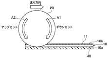
- the dicing cut by the dicing blade 20 is performed in a state where the SiC semiconductor wafer 10 is held as shown in FIG. 2 and the dicing tape 40 is attached so that the chips do not shift after the division.
- a dicing cut in any rotation direction may be used, but a down cut is more preferable in consideration of a reduction in residual stress and a blade wear amount after the dicing cut in addition to a chipping reduction as described later.
- the dicing blade 20 performs dicing cutting from the back surface 10b side serving as the C surface, the entire back surface 10b is covered with the back electrode 11, and the scribe line cannot be confirmed.
- a SiC semiconductor wafer 10 is prepared in a state where a scribe line is determined by forming a device. Then, as shown in FIG. 3B, dicing cut is performed along the scribe line from the surface 10a side to form reference lines 12 and 13 in the X direction and the Y direction, respectively.
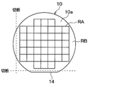
- the reference lines 12 and 13 may be the outermost lines of the effective area RA taken out as a chip. However, in the invalid area RB which is not a chip here, the reference lines 12 and 13 are located at a position away from the effective area RA which is a chip by a predetermined distance. To be formed. The distance from the reference lines 12 and 13 to the effective area RA may be the same or different.
- the effective area RA is an inner area of the SiC semiconductor wafer 10 that avoids an arc-shaped outer edge
- the invalid area RB is a portion located outside the effective area RA.
- the reference lines 12 and 13 are formed in a state where scribe lines can be confirmed, and are formed by dicing cutting the SiC semiconductor wafer 10 from the surface 10a side. For this reason, when the reference lines 12 and 13 are formed, the blade of the dicing blade 20 is inserted in the direction from the Si surface side to the C surface side, and there is a concern that chipping may occur. Therefore, the reference lines 12 and 13 may be the outermost lines of the effective area RA, but it is preferable to form the reference lines 12 and 13 in the invalid area RB in consideration of occurrence of chipping.
- two reference lines 12, 13 are formed, that is, lines parallel to the orthogonal X direction and Y direction are formed.
- the orientation flat 14 is one of the reference lines 12 and 13, while in the present embodiment, the reference line 13 Can also be used. That is, if the orientation flat 14 is formed in the X direction or the Y direction, the reference lines 12 and 13 can be used in this direction.
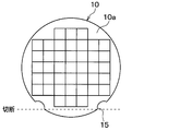
- notches 15 that are notches are formed as the SiC semiconductor wafer 10 instead of the orientation flat 14.
- the reference lines 12 and 13 may be formed along the X direction or the Y direction at the position where the notch 15 is formed, as indicated by a broken line in the drawing.
- the dicing tape 40 is attached to the front surface 10a side of the SiC semiconductor wafer 10 as described above, and dicing cut is performed by the dicing blade 20 from the back surface 10b side.
- the scribe line is recognized with reference to the reference lines 12 and 13, and the dicing blade 20 in the X direction and the Y direction along the scribe line.
- Dicing cut is performed by scanning. That is, since the reference lines 12 and 13 are formed at a predetermined distance from the effective area RA, the scribe line can be estimated using the reference lines 12 and 13 as a reference. Thereby, even if the scribe line cannot be visually recognized by the back electrode 11, it becomes possible to accurately perform dicing cut along the scribe line with reference to the reference lines 12 and 13, and accurately divide into chips. be able to.
- the reference lines 12 and 13 are formed in the invalid area RB, specifically, at a position away from the effective area RA by a predetermined distance. For this reason, even if chipping occurs when the reference lines 12 and 13 are formed, it is possible to remove the portion where the chipping has occurred when a new dicing cut is performed on the scribe line. Therefore, chipping can be suppressed in the manufactured chip.
- the back electrode 11 is formed after the back surface 10b is thinned by grinding or the like in order to reduce the resistance of the vertical semiconductor element, that is, to reduce the on-resistance. ing.
- the thickness of the SiC semiconductor wafer 10 is, for example, 125 ⁇ m or less, preferably 100 ⁇ m or less. Since such a thin SiC semiconductor wafer 10 is diced and cut, the width of the dicing blade 20 (hereinafter referred to as the blade width), the feed speed in the traveling direction, and the rotation direction are defined in order to suppress the occurrence of chipping. ing.
- FIG. 5 is a chart showing the processing conditions. A plurality of workpieces composed of the SiC semiconductor wafer 10 were prepared, and dicing cut was performed on each workpiece under different conditions.
- a workpiece having an effective area RA of 30 mm ⁇ was prepared, and a chip having an index of 2 mm ⁇ 2 mm was prepared. Further, as the dicing cut direction, the CH1 direction as the (1-100) direction is performed, and then the CH2 direction as the (11-20) direction is performed. However, the order may be reversed. Alternatively, it may be performed alternately.
- the blade width of the dicing blade 20 was 40 ⁇ m, the rotation speed was 30000 rotations / min, and the dicing cut direction was both up-cut and down-cut. Further, dicing cutting was performed by switching the feed speed in the moving direction of the dicing blade 20 in three stages of 10, 20, and 30 mm / S. That is, the feed speed was switched in the up cut to perform dicing cut on the three workpieces, and the feed speed was switched in the down cut to perform dicing cut on the three workpieces.
- the amount of cutting water and the amount of cooling water that is, the amount of water supplied to the cut surface side of the dicing blade 20 and the amount of water supplied to both end surfaces of the dicing blade 20 were both set to 1 L / min. Such dicing cut was performed for each of the case where the upper surface of the workpiece to be diced was the Si surface and the C surface.
- any four of the divided chips were extracted for each workpiece, and the state of chipping was examined.
- four samples arranged at symmetrical positions around the workpiece center were used as samples.
- the chipping amount shown in the figure represents the size of chipping.
- the chipping amount Max the value that maximizes the chipping amount is described as the chipping amount Max. is there.
- FIG. 9 is not a sectional view, hatching is shown at the chipping portion.
- the average value of the chipping amounts Max on each of the four sides is described as the chipping amount Ave.
- the position where the chipping amount Max is set is described as the Max position.
- the residual stress is a residual stress in the sample after dicing cut, and the sample was confirmed by performing Raman spectroscopic analysis based on an optical microscope image.
- the blade wear amount the amount of change in the outer diameter of the dicing blade 20 before and after the dicing cut was examined.
- the chipping amount Max is as large as 170 ⁇ m and 79 ⁇ m regardless of whether the cutting direction is down-cut or up-cut.
- the average chipping amount Ave was also a large value of 108.2 ⁇ m and 40.5 ⁇ m.
- the maximum value Max was 90.2 Mpa and 85.7 Mpa, and the average value Ave was also large, 78.1 Mpa and 78.2 Mpa.
- the average value Ave was not so high at 1.9 ⁇ m / m in the case of downcut, but the average value Ave was increased to 3.7 ⁇ m / m in the case of upcut.
- the chipping amount Max is as small as 29 ⁇ m and 36 ⁇ m regardless of whether the cutting direction is down-cut or up-cut.
- the chipping amount Ave was also as small as 18.2 ⁇ m and 25.8 ⁇ m.
- the maximum value Max was 57.2 Mpa and 53.5 Mpa in both cases of the down cut and the up cut, and the average value Ave was a small value of 49.2 Mpa and 48.9 Mpa.
- the average value Ave was not so high at 1.8 ⁇ m / m in the case of up-cutting, but the average value Ave was as small as 1.0 ⁇ m / m in the case of down-cutting. It was.
- the chipping amount can be reduced and the residual stress can be reduced compared to the case of using the Si surface as the processing upper surface for dicing cut. It turns out that it becomes possible.
- the blade wear amount can also be reduced by making the upper surface of the dicing cut the C surface, and the blade wear amount can be significantly reduced by making the cutting direction down cut. It becomes.
- the blade wear amount was also confirmed, but this is because there is a correlation between the chipping amount and the blade width of the dicing blade 20. That is, as the blade width increases, the amount of blade wear can be reduced. However, as the blade width increases, the amount of chipping increases, so the blade width needs to be less than a certain width. Even if the blade width is increased, the chipping amount can be reduced by reducing the feed speed in the moving direction of the dicing blade 20 at the time of dicing cut. However, it is desirable to increase the feed speed from the viewpoint of throughput.
- the cutting direction and the processing upper surface should be either the Si surface or the C surface while keeping the blade width below a certain width. Therefore, it is necessary to reduce the amount of wear based on the above.
- FIG. 10 shows the results when the chipping amount was examined by using the dicing blade 20 having a blade width t of 40 ⁇ m, 70 ⁇ m, and 100 ⁇ m and changing the feed speed in the moving direction of the dicing blade 20.
- the workpiece is diced and cut from the C surface side by down-cutting, and the chipping amounts on the front and back surfaces of the workpiece are examined.
- the chipping amount could be kept small regardless of whether the feed rate was 10 mm / sec or 15 mm / sec.
- the blade width is 70 ⁇ m and 100 ⁇ m, only the chipping amount on the surface side of the workpiece when the feed speed is 10 mm / sec is suppressed, but in other cases the chipping amount could not be suppressed.
- the chipping amount increased as the feed rate increased.
- the blade feed speed at the time of dicing cut is generally 3 to 5 mm / sec, and even if the blade width is wide in this speed range, the chipping amount can be kept small, but high throughput cannot be obtained.
- the feed rate is preferably 10 mm / sec or more, and more preferably 15 mm / sec or more.
- the blade width that can reduce the chipping amount even at such a feed rate is preferably 40 ⁇ m or less. Then, in order to further reduce the amount of wear of the dicing blade 20, it is preferable to make the cut direction down-cut.
- the reference lines 12 and 13 are formed before the dicing cut when the back surface 10b of the SiC semiconductor wafer 10 is covered with the back surface electrode 11 and the scribe line cannot be confirmed. Yes. For this reason, even when the processing upper surface of the dicing cut is the C plane, it is possible to estimate the scribe line based on the reference lines 12 and 13 and perform the dicing cut. Thereby, it can divide
- the thickness of the SiC semiconductor wafer 10 is thin, specifically, 125 ⁇ m or less, chipping is likely to occur.
- dicing cut can be performed from the C surface side, chipping is suppressed and residual stress is reduced. It becomes possible to reduce.
- the blade width of the dicing blade 20 to 40 ⁇ m or less, it is possible to suppress chipping even if the feeding speed at the time of dicing cut is increased.
- the amount of wear of the dicing blade 20 can be reduced by setting the cutting direction of the dicing cut to a down cut.
- the residual stress becomes the smallest when the upper surface of the dicing cut is C-plane and the cut direction is up-cut. For this reason, depending on the pattern configuration of the device and the cutting pitch at which the dicing cut is performed, it is possible to reduce the residual stress by setting the cutting direction to an upcut.
- a vertical semiconductor element is given as an example of a semiconductor element formed on the SiC semiconductor wafer 10, but an example of a structure in which a C surface that is a processing upper surface of a dicing cut is covered with a creeping electrode is given. Only. That is, since the same problem as described above occurs in the dicing cut in the case where the C surface side is entirely covered with the electrode, a semiconductor to which the same structure is applied even if it is other than the vertical semiconductor element
- the above embodiment can also be applied to elements. For example, there is a case where a back electrode is formed in order to fix the C surface side to the ground potential.
- the formation of the reference lines 12 and 13 can be performed by various processing methods or cutting methods including various dicing methods.
- the reference lines 12 and 13 can be formed by various processing methods or cutting methods, such as breaking by dividing with a cut line, laser dicing, dicing blade or braking after half-cutting by laser dicing.
- a bar (-) should be added above a desired number, but there is a limitation in expression based on an electronic application. A bar shall be placed in front of the number.
Landscapes
- Dicing (AREA)
Abstract
SiC半導体ウェハ(10)のうちC面とされる裏面(10b)が裏面電極(11)で覆われてスクライブラインが確認できない場合において、ダイシングカット前に目安線(12、13)を形成する。これにより、ダイシングカットの加工上面をC面とする場合であっても、目安線(12、13)を基準としてスクライブラインを推定してダイシングカットを行うことが可能となる。従って、従来よりも高速に切断しても、チッピングの少ない高品質なSiC半導体装置を製造でき、ブレード摩耗も少なく低コスト化も可能となる。
Description
本出願は、2016年6月22日に出願された日本特許出願番号2016-123898号に基づくもので、ここにその記載内容が参照により組み入れられる。
本開示は、縦型半導体素子を形成した炭化珪素(以下、SiCという)半導体ウェハをチップ単位に分割してSiC半導体装置を製造するSiC半導体装置の製造方法に関するものである。
従来より、SiC半導体ウェハに対してデバイス形成を行ったのち、ダイシングブレードによるダイシングカットによってSiC半導体ウェハをチップ単位に分割し、SiC半導体装置を製造している。このとき、より低抵抗なデバイスとするために、SiC半導体ウェハを薄く研削などで加工してから、チップ単位に分割を行っているが、SiC半導体ウェハを薄くしているために、チップにチッピングと呼ばれる欠けが発生し易くなる。特に、ダイヤモンドに近い硬度を有するSiC単結晶では、劈開性を併せ持ち、加工条件によっては、チップの表裏面や側面のチッピングを誘発させる。このチッピングがのちの組み付けなどにおいて異種材料との応力差によるチップの欠けや割れに繋がり得るため、ダイシングカット時のチッピングを低減することが重要である。
そこで、特許文献1において、SiC半導体ウェハをチップ単位に分割する際のチッピングの発生を抑制する方法が提案されている。具体的には、ダイシングブレードの回転方向をSiC半導体ウェハにおけるC面側からSi面側に向かう方向とすることで、チッピングを抑制している。
しかしながら、SiC半導体ウェハに対して縦型半導体素子を形成する場合、表面側がSi面とされ、裏面側がC面とされることがあり、その場合には、裏面の全面に裏面電極が形成されて、ダイシングカットを行うスクライブラインを認識することができない。このため、的確にチップ単位に分割することができないという問題が発生する。
本開示は上記点に鑑みて、SiC半導体ウェハのC面側が電極で覆われる場合であっても、的確にチップ単位に分割することができるSiC半導体装置の製造方法を提供することを目的とする。
本開示の1つの観点における炭化珪素半導体装置の製造方法は、表面がSi面とされると共に裏面がC面とされ、半導体素子が形成されていると共に、裏面のうち少なくとも半導体素子が形成された部分が裏面電極によって覆われた半導体ウェハを用意することと、半導体ウェハの表面より、スクライブラインに沿った目安線を形成することと、裏面電極が形成された状態で、目安線を基準として裏面側からダイシングブレードによるダイシングカットを行って有効領域をチップ単位に分割することと、を含んでいる。
このように、SiC半導体ウェハのうちC面とされる裏面が裏面電極で覆われてスクライブラインが確認できない場合において、ダイシングカット前に目安線を形成するようにしている。このため、ダイシングカットの加工上面をC面とする場合であっても、目安線を基準としてスクライブラインを推定してダイシングカットを行うことが可能となる。これにより、的確にチップ単位に分割することができる。
以下、本開示の実施形態について図に基づいて説明する。なお、以下の各実施形態相互において、互いに同一もしくは均等である部分には、同一符号を付して説明を行う。
(第1実施形態)
第1実施形態にかかるSiC半導体装置の製造方法について説明する。なお、SiC半導体装置を製造する際には、SiC半導体ウェハに対してデバイス製造プロセスを施したのち、チップ単位に分割するというプロセスを経るが、デバイス製造プロセスについては従来と同様であるため、チップ単位に分割するプロセスについて説明する。
第1実施形態にかかるSiC半導体装置の製造方法について説明する。なお、SiC半導体装置を製造する際には、SiC半導体ウェハに対してデバイス製造プロセスを施したのち、チップ単位に分割するというプロセスを経るが、デバイス製造プロセスについては従来と同様であるため、チップ単位に分割するプロセスについて説明する。
図1に示すように、デバイス製造プロセスを経たSiC半導体ウェハ10を用意する。このSiC半導体ウェハ10は、表面10a側がSi面、裏面10b側がC面とされている。SiC半導体ウェハ10には、デバイスとして縦型半導体素子、例えばMOSFETやショットキーダイオードなどが形成されており、裏面10bの全面が裏面電極11によって覆われている。
このような縦型半導体素子が形成されたSiC半導体ウェハ10をダイシングブレード20にて切断することで、チップ単位に分割し、SiC半導体装置のチップ30を製造する。具体的には、SiC半導体ウェハ10の表面10a上における一方向をX方向、X方向に対して垂直な方向をY方向とするXY平面上において、ダイシングブレード20を走査し、所定のサイズの半導体チップを製造している。例えば、SiC半導体ウェハ10として、表面10aが(0001)面、裏面10bが(000-1)面のものを用い、X方向を(1-100)、Y方向を(11-20)として、X方向およびY方向にダイシングカットを行う。
このとき、SiC半導体ウェハ10にチッピングが発生することを抑制するために、C面とされた裏面10b側にダイシングブレード20を配置し、ダイシングブレード20の刃を裏面10b側から表面10a側に向かう方向に入れるようにしてダイシングカットを行う。つまり、裏面10b側にダイシングブレード20を配置し、C面側からSi面側に向かう方向に刃を入れるようにしている。
ダイシングブレード20によるダイシングカットについては、図2に示すようにSiC半導体ウェハ10を保持して、分割後にチップがズレたりしないように、ダイシングテープ40を貼り付けた状態で行っている。また、ダイシングブレード20の回転方向については2方向ある。具体的には、図2の紙面右方向がダイシングブレード20の進行方向とした場合において、矢印A1のようにダイシングブレード20の刃が上から下に向かうダウンカットと、矢印A2のようにダイシングブレード20の刃が下から上に向かうアップカットがある。いずれの回転方向のダイシングカットであっても良いが、後述するようにチッピング低減に加えて、ダイシングカット後の残留応力やブレード摩耗量の低減などを加味すると、ダウンカットの方が好ましい。
ただし、C面となる裏面10b側よりダイシングブレード20にてダイシングカットを行うようにすることから、裏面10bの全面が裏面電極11によって覆われており、スクライブラインを確認することができない。
このため、チップ単位にダイシングカットを行う前に、スクライブラインを確認できるようにするための処理を行う。
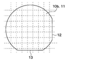
具体的には、図3Aに示すように、デバイス形成を行ってスクライブラインが決まった状態のSiC半導体ウェハ10を用意する。そして、図3Bに示すように、表面10a側からスクライブラインに沿ってダイシングカットを行い、X方向とY方向それぞれの目安線12、13を形成する。目安線12、13については、チップとして取り出される有効領域RAの最も外側のラインとしても良いが、ここではチップとされない無効領域RB内において、チップとされる有効領域RAから所定距離離れた位置に形成されるようにしている。目安線12、13から有効領域RAまでの距離は同じであっても良いし、異なっていても良い。なお、有効領域RAは、SiC半導体ウェハ10のうち円弧状となる外縁部を避けた内側の領域であり、無効領域RBは、有効領域RAの外側に位置する部分である。
目安線12、13については、スクライブラインが確認できる状態で形成しており、SiC半導体ウェハ10を表面10a側からダイシングカットすることによって形成している。このため、目安線12、13を形成する際には、Si面側からC面側に向かう方向にダイシングブレード20の刃が入れられることになり、チッピングの発生が懸念される。したがって、目安線12、13を有効領域RAの最も外側のラインとしても良いが、チッピングの発生を考慮すると、無効領域RB内に目安線12、13を形成することが好ましい。このように、目安線12、13を有効領域RAから所定距離離れた位置に形成されるようにすることで、目安線12、13の形成時にチッピングが発生したとしても、最終的に形成されるチップの端面でのチッピングの発生を抑制できるようにしている。
なお、ここでは目安線12、13の2本、つまり直交するX方向とY方向それぞれに平行な線を形成するようにした。しかしながら、図3Aに示すように、SiC半導体ウェハ10にオリエンテーションフラット(以下、オリフラと言う)14が形成される場合、オリフラ14を目安線12、13の一方、本実施形態の場合は目安線13として用いることもできる。すなわち、オリフラ14がX方向もしくはY方向に形成されているのであれば、当該方向について、目安線12、13の代わりとすることができる。
また、図4に示すように、オリフラ14ではなく、SiC半導体ウェハ10として、切り欠きであるノッチ15が形成されているものもある。この場合には、図中破線で示したように、ノッチ15が形成された位置などにおいて、X方向もしくはY方向に沿って目安線12、13を形成すれば良い。
このようにして目安線12、13を形成したら、その後に、上記したようにSiC半導体ウェハ10の表面10a側にダイシングテープ40を貼り付け、裏面10b側からダイシングブレード20によってダイシングカットを行う。このとき、SiC半導体ウェハ10に対して目安線12、13を形成してあるため、目安線12、13を基準としてスクライブラインを認識し、スクライブラインに沿ってX方向およびY方向にダイシングブレード20を走査することでダイシングカットを行う。すなわち、目安線12、13の形成位置が有効領域RAから所定距離の位置としているため、目安線12、13を基準としてスクライブラインを推定することができる。これにより、裏面電極11によってスクライブラインを視認することができなくても、目安線12、13を基準として的確にスクライブラインに沿ってダイシングカットを行うことが可能となり、的確にチップ単位に分割することができる。
また、上記したように、目安線12、13を無効領域RB内、具体的には有効領域RAから所定距離離れた位置に形成するようにしている。このため、仮に目安線12、13を形成する際にチッピングが発生していたとしても、新たにスクライブラインでダイシングカットを行ったときに、チッピングが発生した部分を除去することが可能となる。したがって、製造後のチップは、チッピングが抑制されたものとすることができる。
続いて、ダイシングカットの加工条件について説明する。
ダイシングカットが行われるSiC半導体ウェハ10については、縦型半導体素子の低抵抗化、つまりオン抵抗低減のために、裏面10bを研削などで加工して薄くしてから裏面電極11を形成するようにしている。このため、SiC半導体ウェハ10の厚みは、例えば125μm以下とされ、好ましくは100μm以下とされる。そして、このように薄いSiC半導体ウェハ10をダイシングカットすることから、チッピングの発生を抑制すべく、ダイシングブレード20の幅(以下、ブレード幅という)や進行方向への送り速度、回転方向を規定している。
図5は、加工条件を示した図表である。SiC半導体ウェハ10で構成されるワークを複数用意し、各ワークに対して条件を変えてダイシングカットを行った。
ワークとしては、図6に示すように、有効領域RAの寸法を30mm□とするものを用意し、Indexが2mm×2mmとなるチップを作製するようにした。また、ダイシングカットの方向としては、(1-100)方向となるCH1の方向を行った後、(11-20)方向となるCH2の方向を行うようにしたが、順序を逆としても良いし、交互に行ってもよい。
ダイシングブレード20のブレード幅については40μmとしており、回転数を30000回転/minとし、ダイシングカットの方向についてはアップカットとダウンカットの両方について行った。さらに、ダイシングブレード20の移動方向への送り速度を10、20、30mm/Sの3段階で切替えてダイシングカットを行った。すなわち、アップカットにおいて送り速度を切替えて3つのワークに対してダイシングカットを行うとともに、ダウンカットにおいて送り速度を切替えて3つのワークに対してダイシングカットを行った。切削水量や冷却水量、すなわちダイシングブレード20の切断面側への供給水量やダイシングブレード20の両端面側への供給水量については、共に、1L/minとした。そして、このようなダイシングカットを、ダイシングするワークの加工上面をSi面とする場合とC面とする場合それぞれについて行った。
このようなダイシングカットを行った後、各ワークについて、図6中にハッチングで示したように、分割した複数のチップの中の任意の4つを抜き出して、チッピングの様子を調べた。ここでは、ワーク中心を中心とした対称位置に配置されている4つをサンプルとした。
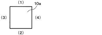
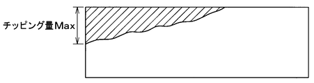
チッピングの様子については、図7Aに示すようにチップの表面10a側と、図7Bに示すようにチップの裏面10b側と、4つの断面(1)~(4)のそれぞれ、つまり合計12箇所について確認したところ、図8に示す結果となった。図中に示したチッピング量とは、チッピングの大きさ表しており、図9に示すように深さが変化しているチッピングの場合、チッピング量が最大となる値をチッピング量Maxとして記載してある。図9は断面図ではないが、チッピング箇所にハッチングを示してある。また、4辺それぞれにおけるチッピング量Maxの平均値をチッピング量Aveとして記載してある。さらに、チッピング量Maxとなっていた位置をMax位置として記載してある。
さらに、残留応力とは、ダイシングカット後におけるサンプル中の残留応力のことであり、サンプルについて光学顕微鏡画像に基づいてラマン分光分析を行うことで確認を行った。ブレード摩耗量については、ダイシングカット前後でのダイシングブレード20の外径の変化量を調べた。
その結果、図8に示すように、ダイシングカットを行う加工面の上面をSi面とする場合には、カット方向がダウンカット、アップカットいずれの場合にも、チッピング量Maxが170μm、79μmと大きな値となり、平均のチッピング量Aveについても108.2μm、40.5μmと大きな値となっていた。残留応力についても、カット方向を変えても最大値Maxが90.2Mpa、85.7Mpaとなり、平均値Aveも78.1Mpa、78.2Mpaと大きな値となった。ブレード摩耗量については、ダウンカットの場合は平均値Aveが1.9μm/mとさほど多くなかったが、アップカットの場合には平均値Aveが3.7μm/mと多くなった。
これに対して、ダイシングカットを行う加工面の上面をC面とする場合には、カット方向がダウンカット、アップカットいずれの場合にも、チッピング量Maxが29μm、36μmと小さな値となり、平均のチッピング量Aveについても18.2μm、25.8μmと小さな値となっていた。残留応力についても、ダウンカット、アップカットいずれの場合にも最大値Maxが57.2Mpa、53.5Mpaとなり、平均値Aveも49.2Mpa、48.9Mpaと小さな値となった。ブレード摩耗量については、アップカットの場合にも、平均値Aveが1.8μm/mとさほど多くなかったが、ダウンカットの場合には、平均値Aveが1.0μm/mと小さな値であった。
これらの実験結果に基づき、ダイシングカットを行う加工上面をC面とすることで、Si面とする場合と比較して、チッピング量を減少させることが可能になるし、残留応力についても低減することが可能になることが判る。また、ブレード摩耗量についても、ダイシングカットを行う加工上面をC面とすることで低減することが可能となり、特にカット方向をダウンカットとすることで、顕著にブレード摩耗量を低減することが可能となる。
ここで、上記実験では、ブレード摩耗量についても確認したが、これはチッピング量とダイシングブレード20のブレード幅との間に相関関係があるためである。すなわち、ブレード幅が厚くなるほどブレード摩耗量を減らすことができるものの、ブレード幅を厚くするとチッピング量が大きくなるため、ブレード幅をある程度の幅以下にする必要がある。ブレード幅を厚くしたとしても、ダイシングカット時におけるダイシングブレード20の移動方向への送り速度を遅くすればチッピング量を小さくできるが、スループットの観点からは送り速度を早くすることが望ましい。このため、送り速度を早くしつつ、ダイシングブレード20の摩耗量を少なく抑えるには、ブレード幅をある程度の幅以下にしつつも、カット方向や加工上面をSi面とC面のいずれにするかなどに基づき摩耗量の低減を図ることが必要になる。
図10は、ブレード幅tを40μm、70μm、100μmとしたダイシングブレード20を用い、ダイシングブレード20の移動方向への送り速度を変えてチッピング量を調べたときの結果を示している。ここでは、SiC半導体ウェハ10で構成されるワークのC面を加工上面として、C面側からダウンカットでワークをダイシングカットし、ワークの表面と裏面それぞれでのチッピング量を調べている。
この図に示されるように、ブレード幅を40μmとした場合には、送り速度が10mm/sec、15mm/secいずれの場合であっても、チッピング量を小さく抑えることができていた。これに対して、ブレード幅を70μm、100μmとした場合には、送り速度を10mm/secとした場合のワークの表面側のチッピング量についてのみ抑えられていたが、それ以外の場合にはチッピング量を抑えることができていなかった。特に、送り速度が早くなるほど、チッピング量が増大していた。
従来では、一般的にダイシングカット時におけるブレードの送り速度が3~5mm/secとされ、この速度域ではブレード幅が広かったとしてもチッピング量は小さく抑えることができるが、高いスループットが得られない。高いスループットが得られるようにするためには、例えば送り速度を10mm/sec以上とするのが好ましく、より好ましくは15mm/sec以上にすると良い。このような送り速度としてもチッピング量を低減できるブレード幅は40μm以下とすることが好ましい。そして、ダイシングブレード20の摩耗量をより低減するために、カット方向をダウンカットにすると良い。
以上説明したように、SiC半導体ウェハ10のうちC面とされる裏面10bが裏面電極11で覆われてスクライブラインが確認できない場合において、ダイシングカット前に目安線12、13を形成するようにしている。このため、ダイシングカットの加工上面をC面とする場合であっても、目安線12、13を基準としてスクライブラインを推定してダイシングカットを行うことが可能となる。これにより、的確にチップ単位に分割することができる。
また、SiC半導体ウェハ10の厚みを薄く、具体的には125μm以下とするような場合にはチッピングが発生し易くなるが、C面側からダイシングカットできることから、チッピングを抑制することや残留応力を低減することが可能となる。特に、ダイシングブレード20のブレード幅を40μm以下とすることで、ダイシングカット時の送り速度を高くしてもチッピングを抑制することが可能となる。さらに、ダイシングカットのカット方向をダウンカットとすることで、ダイシングブレード20の摩耗量を低減することが可能となる。
また、残留応力の観点から言えば、ダイシングカットの加工上面をC面とし、カット方向をアップカットとする場合に最も残留応力が小さくなる。このため、デバイスのパターン構成やダイシングカットを行う切断ピッチによっては、カット方向をアップカットとすることで、残留応力を小さくすることも可能となる。
(他の実施形態)
本開示は、上記した実施形態に準拠して記述されたが、当該実施形態に限定されるものではなく、様々な変形例や均等範囲内の変形をも包含する。加えて、様々な組み合わせや形態、さらには、それらに一要素のみ、それ以上、あるいはそれ以下、を含む他の組み合わせや形態をも、本開示の範疇や思想範囲に入るものである。
本開示は、上記した実施形態に準拠して記述されたが、当該実施形態に限定されるものではなく、様々な変形例や均等範囲内の変形をも包含する。加えて、様々な組み合わせや形態、さらには、それらに一要素のみ、それ以上、あるいはそれ以下、を含む他の組み合わせや形態をも、本開示の範疇や思想範囲に入るものである。
例えば、上記実施形態では、SiC半導体ウェハ10に形成される半導体素子として縦型半導体素子を例として挙げたが、ダイシングカットの加工上面となるC面が沿面電極によって覆われる構造の一例を挙げたに過ぎない。すなわち、C面側が電極によって全面覆われるような構造とされる場合のダイシングカットの際に上記と同様の問題が発生するため、縦型半導体素子以外であっても同様の構造が適用される半導体素子についても上記実施形態を適用できる。例えば、C面側を接地電位に固定するために裏面電極を形成するような構造とされる場合が挙げられる。
また、C面の全面が裏面電極11によって覆われる場合について説明したが、少なくともチップ化される半導体素子が形成された部分が裏面電極11によって覆われて、スクライブラインが確認し難くなる構造について、上記実施形態と適用できる。
また、上記実施形態では、目安線12、13として、直線状に無効領域RBの一部の円弧部分を切断したものを形成したが、表面10a側からダイシングカットすることで、裏面10bからも確認できる印となる目安線12、13が形成されていれば良い。このため、無効領域RBの一部の円弧部分を除去するように切断していなくても、一部を切り欠くことで目安線12、13を形成しても良い。
さらに、目安線12、13の形成については、様々なダイシング方法を含む様々な加工方法もしくは切断方法によって行える。例えば、切れ目線を入れて分割するブレーキング、レーザダイシング、ダイシングブレードもしくはレーザダイシングでハーフカットを行ってからのブレーキングなど、様々な加工方法もしくは切断方法によって目安線12、13を形成できる。
なお、結晶の方位を示す場合、本来ならば所望の数字の上にバー(-)を付すべきであるが、電子出願に基づく表現上の制限が存在するため、本明細書においては、所望の数字の前にバーを付すものとする。
Claims (6)
- 表面(10a)がSi面とされると共に裏面(10b)がC面とされ、半導体素子が形成されていると共に、前記裏面のうち少なくとも前記半導体素子が形成された部分が裏面電極(11)によって覆われた半導体ウェハ(10)を用意することと、
前記表面より、前記スクライブラインに沿った目安線(12、13)を形成することと、
前記裏面電極が形成された状態で、前記目安線を基準として前記裏面側からダイシングブレード(20)によるダイシングカットを行って前記有効領域をチップ単位に分割することと、を含んでいる炭化珪素半導体装置の製造方法。 - 前記半導体ウェハのうち、前記半導体素子が形成された部分を前記ダイシングカットにて前記スクライブラインに沿ってチップ単位に分割する有効領域(RA)とし、前記有効領域の外側を無効領域(RB)として、
前記目安線を形成することでは、前記無効領域内において、前記表面からダイシングカットすることで、前記有効領域から離れた位置に前記目安線を形成する請求項1に記載の炭化珪素半導体装置の製造方法。 - 前記チップ単位に分割することでは、前記ダイシングブレードとしてブレード幅が40μm以下のものを用いる請求項1または2に記載の炭化珪素半導体装置の製造方法。
- 前記チップ単位に分割することでは、前記ダイシングブレードの送り速度を10mm/sec以上とする請求項3に記載の炭化珪素半導体装置の製造方法。
- 前記チップ単位に分割することでは、前記半導体ウェハの切断部において、前記ダイシングブレードの刃が上から下に向かうダウンカットにより前記チップ単位に分割する請求項1ないし4のいずれか1つに記載の炭化珪素半導体装置の製造方法。
- 前記半導体ウェハを用意することにおいて、前記半導体ウェハとして前記スクライブラインの一方向と平行なオリエンテーションフラット(14)が形成されているものを用意し、
前記目安線を形成することでは、前記目安線として、前記オリエンテーションフラットに対して垂直な方向のものを第1目安線として前記ダイシングカットによって形成し、
前記チップ単位に分割することでは、前記オリエンテーションフラットを第2目安線として、前記第1目安線と前記第2目安線を基準として前記チップ単位に分割する請求項1ないし5のいずれか1つに記載の炭化珪素半導体装置の製造方法。
Priority Applications (1)
| Application Number | Priority Date | Filing Date | Title |
|---|---|---|---|
| US16/082,570 US20190035684A1 (en) | 2016-06-22 | 2017-05-11 | Method for manufacturing silicon carbide semiconductor device |
Applications Claiming Priority (2)
| Application Number | Priority Date | Filing Date | Title |
|---|---|---|---|
| JP2016123898A JP6497358B2 (ja) | 2016-06-22 | 2016-06-22 | 炭化珪素半導体装置の製造方法 |
| JP2016-123898 | 2016-06-22 |
Publications (1)
| Publication Number | Publication Date |
|---|---|
| WO2017221577A1 true WO2017221577A1 (ja) | 2017-12-28 |
Family
ID=60784296
Family Applications (1)
| Application Number | Title | Priority Date | Filing Date |
|---|---|---|---|
| PCT/JP2017/017873 Ceased WO2017221577A1 (ja) | 2016-06-22 | 2017-05-11 | 炭化珪素半導体装置の製造方法 |
Country Status (3)
| Country | Link |
|---|---|
| US (1) | US20190035684A1 (ja) |
| JP (1) | JP6497358B2 (ja) |
| WO (1) | WO2017221577A1 (ja) |
Cited By (2)
| Publication number | Priority date | Publication date | Assignee | Title |
|---|---|---|---|---|
| JP7050658B2 (ja) | 2018-12-18 | 2022-04-08 | 三菱電機株式会社 | 半導体チップの製造方法 |
| US11309188B2 (en) | 2018-05-09 | 2022-04-19 | Semiconductor Components Industries, Llc | Singulation of silicon carbide semiconductor wafers |
Families Citing this family (7)
| Publication number | Priority date | Publication date | Assignee | Title |
|---|---|---|---|---|
| JPWO2020144790A1 (ja) * | 2019-01-10 | 2021-02-18 | 三菱電機株式会社 | 電力用半導体装置 |
| WO2020183580A1 (ja) * | 2019-03-11 | 2020-09-17 | 株式会社オプト・システム | 半導体チップの製造方法 |
| CN114026672B (zh) * | 2019-06-13 | 2025-03-11 | 住友电气工业株式会社 | 碳化硅衬底和碳化硅衬底的制造方法 |
| JP7325911B2 (ja) | 2019-10-16 | 2023-08-15 | 株式会社ディスコ | 被加工物の加工方法 |
| CN110789010A (zh) * | 2019-11-01 | 2020-02-14 | 常州时创能源科技有限公司 | 晶硅边皮料的切割工艺 |
| JPWO2023058510A1 (ja) * | 2021-10-08 | 2023-04-13 | ||
| CN116387134A (zh) * | 2022-08-10 | 2023-07-04 | 廖富江 | 半导体制造方法 |
Citations (4)
| Publication number | Priority date | Publication date | Assignee | Title |
|---|---|---|---|---|
| JP2006086200A (ja) * | 2004-09-14 | 2006-03-30 | Enzan Seisakusho:Kk | 半導体ウェハのダイシング方法 |
| JP2009105211A (ja) * | 2007-10-23 | 2009-05-14 | Disco Abrasive Syst Ltd | ウエーハの分割方法 |
| JP2013161944A (ja) * | 2012-02-06 | 2013-08-19 | Mitsubishi Electric Corp | ダイシング方法 |
| JP2014013812A (ja) * | 2012-07-04 | 2014-01-23 | Disco Abrasive Syst Ltd | SiC基板の加工方法 |
Family Cites Families (12)
| Publication number | Priority date | Publication date | Assignee | Title |
|---|---|---|---|---|
| US5927993A (en) * | 1992-02-03 | 1999-07-27 | Motorola, Inc. | Backside processing method |
| US6165874A (en) * | 1997-07-03 | 2000-12-26 | The United States Of America As Represented By The Administrator Of The National Aeronautics And Space Administration | Method for growth of crystal surfaces and growth of heteroepitaxial single crystal films thereon |
| US6488771B1 (en) * | 2001-09-25 | 2002-12-03 | The United States Of America As Represented By The Administrator Of The National Aeronautics And Space Administration | Method for growing low-defect single crystal heteroepitaxial films |
| TWI222173B (en) * | 2003-08-20 | 2004-10-11 | Advanced Semiconductor Eng | Method of making a package structure by dicing a wafer from the backside surface thereof |
| TWI293474B (en) * | 2005-06-16 | 2008-02-11 | Advanced Semiconductor Eng | A wafer dicting process for optical electronic packing |
| JP2009123835A (ja) * | 2007-11-13 | 2009-06-04 | Disco Abrasive Syst Ltd | 半導体デバイスの製造方法 |
| CN102782804B (zh) * | 2010-05-18 | 2015-02-25 | 松下电器产业株式会社 | 半导体芯片以及半导体芯片的制造方法 |
| JP5914060B2 (ja) * | 2012-03-09 | 2016-05-11 | 三菱電機株式会社 | 炭化珪素半導体装置の製造方法 |
| JP2016009706A (ja) * | 2014-06-23 | 2016-01-18 | 住友電気工業株式会社 | 半導体デバイスの製造方法、半導体基板および半導体デバイス |
| JP6466692B2 (ja) * | 2014-11-05 | 2019-02-06 | 株式会社ディスコ | ウエーハの加工方法 |
| JP6287774B2 (ja) * | 2014-11-19 | 2018-03-07 | 住友電気工業株式会社 | 炭化珪素半導体装置の製造方法 |
| JP6486239B2 (ja) * | 2015-08-18 | 2019-03-20 | 株式会社ディスコ | ウエーハの加工方法 |
-
2016
- 2016-06-22 JP JP2016123898A patent/JP6497358B2/ja active Active
-
2017
- 2017-05-11 WO PCT/JP2017/017873 patent/WO2017221577A1/ja not_active Ceased
- 2017-05-11 US US16/082,570 patent/US20190035684A1/en not_active Abandoned
Patent Citations (4)
| Publication number | Priority date | Publication date | Assignee | Title |
|---|---|---|---|---|
| JP2006086200A (ja) * | 2004-09-14 | 2006-03-30 | Enzan Seisakusho:Kk | 半導体ウェハのダイシング方法 |
| JP2009105211A (ja) * | 2007-10-23 | 2009-05-14 | Disco Abrasive Syst Ltd | ウエーハの分割方法 |
| JP2013161944A (ja) * | 2012-02-06 | 2013-08-19 | Mitsubishi Electric Corp | ダイシング方法 |
| JP2014013812A (ja) * | 2012-07-04 | 2014-01-23 | Disco Abrasive Syst Ltd | SiC基板の加工方法 |
Cited By (3)
| Publication number | Priority date | Publication date | Assignee | Title |
|---|---|---|---|---|
| US11309188B2 (en) | 2018-05-09 | 2022-04-19 | Semiconductor Components Industries, Llc | Singulation of silicon carbide semiconductor wafers |
| US11942327B2 (en) | 2018-05-09 | 2024-03-26 | Semiconductor Components Industries, Llc | Singulation of silicon carbide semiconductor wafers |
| JP7050658B2 (ja) | 2018-12-18 | 2022-04-08 | 三菱電機株式会社 | 半導体チップの製造方法 |
Also Published As
| Publication number | Publication date |
|---|---|
| US20190035684A1 (en) | 2019-01-31 |
| JP2017228660A (ja) | 2017-12-28 |
| JP6497358B2 (ja) | 2019-04-10 |
Similar Documents
| Publication | Publication Date | Title |
|---|---|---|
| JP6497358B2 (ja) | 炭化珪素半導体装置の製造方法 | |
| JP7605915B2 (ja) | 結晶材料を切り分けるためのレーザ・アシスト法 | |
| JP7605917B2 (ja) | 結晶材料を切り分けるためのレーザ・アシスト法 | |
| US20230330769A1 (en) | Parent Substrate, Wafer Composite and Methods of Manufacturing Crystalline Substrates and Semiconductor Devices | |
| JP6132621B2 (ja) | 半導体単結晶インゴットのスライス方法 | |
| CN106531623B (zh) | 加工衬底的方法 | |
| JP2016207908A (ja) | 炭化珪素半導体装置の製造方法および炭化珪素半導体装置 | |
| US20240234155A1 (en) | Singulation of silicon carbide semiconductor wafers | |
| JP6230112B2 (ja) | ウェハの製造方法およびウェハの製造装置 | |
| JP2021034680A (ja) | レーザースライシング装置及びそれを用いたスライシング方法 | |
| JP2013161944A (ja) | ダイシング方法 | |
| KR102501898B1 (ko) | GaN 기판의 분단 방법 | |
| KR102190861B1 (ko) | 스크라이브 방법 및 스크라이브 장치 | |
| US9536838B1 (en) | Single crystal ingot, semiconductor wafer and method of manufacturing semiconductor wafers | |
| JP5886522B2 (ja) | ウェーハ生産方法 | |
| TWI803972B (zh) | 晶錠切割方法 | |
| US20250201566A1 (en) | Method for manufacturing semiconductor apparatus and semiconductor apparatus | |
| JP6705399B2 (ja) | ウェーハの製造方法 | |
| TW201611188A (zh) | 半導體裝置及其製造方法 | |
| WO2023058509A1 (ja) | SiC半導体装置 | |
| CN118077035A (zh) | 半导体装置 | |
| JP2012129285A (ja) | ウェーハ生産方法 |
Legal Events
| Date | Code | Title | Description |
|---|---|---|---|
| 121 | Ep: the epo has been informed by wipo that ep was designated in this application |
Ref document number: 17815047 Country of ref document: EP Kind code of ref document: A1 |
|
| NENP | Non-entry into the national phase |
Ref country code: DE |
|
| 122 | Ep: pct application non-entry in european phase |
Ref document number: 17815047 Country of ref document: EP Kind code of ref document: A1 |