WO2017217454A1 - 有機電子素子の製造方法及び機能層の製造方法 - Google Patents
有機電子素子の製造方法及び機能層の製造方法 Download PDFInfo
- Publication number
- WO2017217454A1 WO2017217454A1 PCT/JP2017/021966 JP2017021966W WO2017217454A1 WO 2017217454 A1 WO2017217454 A1 WO 2017217454A1 JP 2017021966 W JP2017021966 W JP 2017021966W WO 2017217454 A1 WO2017217454 A1 WO 2017217454A1
- Authority
- WO
- WIPO (PCT)
- Prior art keywords
- plastic substrate
- infrared
- coating film
- infrared rays
- cooling
- Prior art date
Links
- 238000004519 manufacturing process Methods 0.000 title claims abstract description 55
- 238000000034 method Methods 0.000 title abstract description 48
- 239000000758 substrate Substances 0.000 claims abstract description 200
- 229920003023 plastic Polymers 0.000 claims abstract description 194
- 239000004033 plastic Substances 0.000 claims abstract description 194
- 238000001816 cooling Methods 0.000 claims abstract description 132
- 238000000576 coating method Methods 0.000 claims abstract description 122
- 238000010438 heat treatment Methods 0.000 claims abstract description 117
- 239000011248 coating agent Substances 0.000 claims abstract description 108
- 239000007788 liquid Substances 0.000 claims abstract description 10
- 230000001678 irradiating effect Effects 0.000 claims abstract description 6
- 239000000463 material Substances 0.000 claims description 59
- 239000002346 layers by function Substances 0.000 claims description 55
- 239000011261 inert gas Substances 0.000 claims description 23
- 238000010521 absorption reaction Methods 0.000 claims description 13
- 238000004132 cross linking Methods 0.000 claims description 4
- 230000015572 biosynthetic process Effects 0.000 abstract description 12
- 239000010410 layer Substances 0.000 description 143
- 239000010408 film Substances 0.000 description 75
- 238000002347 injection Methods 0.000 description 51
- 239000007924 injection Substances 0.000 description 51
- 230000005855 radiation Effects 0.000 description 25
- 230000005525 hole transport Effects 0.000 description 24
- 230000007246 mechanism Effects 0.000 description 23
- -1 polyethylene terephthalate Polymers 0.000 description 19
- 239000007789 gas Substances 0.000 description 16
- 230000004048 modification Effects 0.000 description 14
- 238000012986 modification Methods 0.000 description 14
- 239000000498 cooling water Substances 0.000 description 12
- 239000002904 solvent Substances 0.000 description 9
- 230000004888 barrier function Effects 0.000 description 8
- 238000010586 diagram Methods 0.000 description 8
- 229910052751 metal Inorganic materials 0.000 description 8
- 239000002184 metal Substances 0.000 description 8
- 229910052783 alkali metal Inorganic materials 0.000 description 7
- 230000008569 process Effects 0.000 description 6
- 239000000126 substance Substances 0.000 description 6
- 239000010409 thin film Substances 0.000 description 6
- 150000001340 alkali metals Chemical class 0.000 description 5
- 229910052784 alkaline earth metal Inorganic materials 0.000 description 5
- 150000001342 alkaline earth metals Chemical class 0.000 description 5
- 150000001875 compounds Chemical class 0.000 description 5
- 238000007611 bar coating method Methods 0.000 description 4
- 230000000903 blocking effect Effects 0.000 description 4
- ZYGHJZDHTFUPRJ-UHFFFAOYSA-N coumarin Chemical compound C1=CC=C2OC(=O)C=CC2=C1 ZYGHJZDHTFUPRJ-UHFFFAOYSA-N 0.000 description 4
- 239000002019 doping agent Substances 0.000 description 4
- 239000000975 dye Substances 0.000 description 4
- 238000007756 gravure coating Methods 0.000 description 4
- 238000007641 inkjet printing Methods 0.000 description 4
- 229920000123 polythiophene Polymers 0.000 description 4
- 238000007639 printing Methods 0.000 description 4
- 238000005096 rolling process Methods 0.000 description 4
- 239000000243 solution Substances 0.000 description 4
- ZWEHNKRNPOVVGH-UHFFFAOYSA-N 2-Butanone Chemical compound CCC(C)=O ZWEHNKRNPOVVGH-UHFFFAOYSA-N 0.000 description 3
- CSCPPACGZOOCGX-UHFFFAOYSA-N Acetone Chemical compound CC(C)=O CSCPPACGZOOCGX-UHFFFAOYSA-N 0.000 description 3
- OKTJSMMVPCPJKN-UHFFFAOYSA-N Carbon Chemical compound [C] OKTJSMMVPCPJKN-UHFFFAOYSA-N 0.000 description 3
- YMWUJEATGCHHMB-UHFFFAOYSA-N Dichloromethane Chemical compound ClCCl YMWUJEATGCHHMB-UHFFFAOYSA-N 0.000 description 3
- XEKOWRVHYACXOJ-UHFFFAOYSA-N Ethyl acetate Chemical compound CCOC(C)=O XEKOWRVHYACXOJ-UHFFFAOYSA-N 0.000 description 3
- XUIMIQQOPSSXEZ-UHFFFAOYSA-N Silicon Chemical compound [Si] XUIMIQQOPSSXEZ-UHFFFAOYSA-N 0.000 description 3
- YXFVVABEGXRONW-UHFFFAOYSA-N Toluene Chemical compound CC1=CC=CC=C1 YXFVVABEGXRONW-UHFFFAOYSA-N 0.000 description 3
- 239000012298 atmosphere Substances 0.000 description 3
- QVGXLLKOCUKJST-UHFFFAOYSA-N atomic oxygen Chemical compound [O] QVGXLLKOCUKJST-UHFFFAOYSA-N 0.000 description 3
- 229910052799 carbon Inorganic materials 0.000 description 3
- 238000006243 chemical reaction Methods 0.000 description 3
- 150000004696 coordination complex Chemical class 0.000 description 3
- 238000009792 diffusion process Methods 0.000 description 3
- WASQWSOJHCZDFK-UHFFFAOYSA-N diketene Chemical compound C=C1CC(=O)O1 WASQWSOJHCZDFK-UHFFFAOYSA-N 0.000 description 3
- 230000009477 glass transition Effects 0.000 description 3
- 150000004820 halides Chemical class 0.000 description 3
- 239000001301 oxygen Substances 0.000 description 3
- 229910052760 oxygen Inorganic materials 0.000 description 3
- BASFCYQUMIYNBI-UHFFFAOYSA-N platinum Chemical compound [Pt] BASFCYQUMIYNBI-UHFFFAOYSA-N 0.000 description 3
- 229920000767 polyaniline Polymers 0.000 description 3
- 239000011112 polyethylene naphthalate Substances 0.000 description 3
- 229920000642 polymer Polymers 0.000 description 3
- 239000003507 refrigerant Substances 0.000 description 3
- 229910052710 silicon Inorganic materials 0.000 description 3
- 239000010703 silicon Substances 0.000 description 3
- 150000003553 thiiranes Chemical class 0.000 description 3
- 238000002834 transmittance Methods 0.000 description 3
- VQGHOUODWALEFC-UHFFFAOYSA-N 2-phenylpyridine Chemical compound C1=CC=CC=C1C1=CC=CC=N1 VQGHOUODWALEFC-UHFFFAOYSA-N 0.000 description 2
- HRPVXLWXLXDGHG-UHFFFAOYSA-N Acrylamide Chemical compound NC(=O)C=C HRPVXLWXLXDGHG-UHFFFAOYSA-N 0.000 description 2
- XKRFYHLGVUSROY-UHFFFAOYSA-N Argon Chemical compound [Ar] XKRFYHLGVUSROY-UHFFFAOYSA-N 0.000 description 2
- IJGRMHOSHXDMSA-UHFFFAOYSA-N Atomic nitrogen Chemical compound N#N IJGRMHOSHXDMSA-UHFFFAOYSA-N 0.000 description 2
- BVKZGUZCCUSVTD-UHFFFAOYSA-L Carbonate Chemical compound [O-]C([O-])=O BVKZGUZCCUSVTD-UHFFFAOYSA-L 0.000 description 2
- HEDRZPFGACZZDS-UHFFFAOYSA-N Chloroform Chemical compound ClC(Cl)Cl HEDRZPFGACZZDS-UHFFFAOYSA-N 0.000 description 2
- 229910052693 Europium Inorganic materials 0.000 description 2
- XEEYBQQBJWHFJM-UHFFFAOYSA-N Iron Chemical compound [Fe] XEEYBQQBJWHFJM-UHFFFAOYSA-N 0.000 description 2
- 238000000342 Monte Carlo simulation Methods 0.000 description 2
- 229920001609 Poly(3,4-ethylenedioxythiophene) Polymers 0.000 description 2
- 239000004698 Polyethylene Substances 0.000 description 2
- 239000004743 Polypropylene Substances 0.000 description 2
- KAESVJOAVNADME-UHFFFAOYSA-N Pyrrole Chemical compound C=1C=CNC=1 KAESVJOAVNADME-UHFFFAOYSA-N 0.000 description 2
- NRCMAYZCPIVABH-UHFFFAOYSA-N Quinacridone Chemical compound N1C2=CC=CC=C2C(=O)C2=C1C=C1C(=O)C3=CC=CC=C3NC1=C2 NRCMAYZCPIVABH-UHFFFAOYSA-N 0.000 description 2
- WYURNTSHIVDZCO-UHFFFAOYSA-N Tetrahydrofuran Chemical compound C1CCOC1 WYURNTSHIVDZCO-UHFFFAOYSA-N 0.000 description 2
- QYKIQEUNHZKYBP-UHFFFAOYSA-N Vinyl ether Chemical compound C=COC=C QYKIQEUNHZKYBP-UHFFFAOYSA-N 0.000 description 2
- XLOMVQKBTHCTTD-UHFFFAOYSA-N Zinc monoxide Chemical compound [Zn]=O XLOMVQKBTHCTTD-UHFFFAOYSA-N 0.000 description 2
- MPIAGWXWVAHQBB-UHFFFAOYSA-N [3-prop-2-enoyloxy-2-[[3-prop-2-enoyloxy-2,2-bis(prop-2-enoyloxymethyl)propoxy]methyl]-2-(prop-2-enoyloxymethyl)propyl] prop-2-enoate Chemical compound C=CC(=O)OCC(COC(=O)C=C)(COC(=O)C=C)COCC(COC(=O)C=C)(COC(=O)C=C)COC(=O)C=C MPIAGWXWVAHQBB-UHFFFAOYSA-N 0.000 description 2
- XHCLAFWTIXFWPH-UHFFFAOYSA-N [O-2].[O-2].[O-2].[O-2].[O-2].[V+5].[V+5] Chemical class [O-2].[O-2].[O-2].[O-2].[O-2].[V+5].[V+5] XHCLAFWTIXFWPH-UHFFFAOYSA-N 0.000 description 2
- 239000006096 absorbing agent Substances 0.000 description 2
- 125000003647 acryloyl group Chemical group O=C([*])C([H])=C([H])[H] 0.000 description 2
- HSFWRNGVRCDJHI-UHFFFAOYSA-N alpha-acetylene Natural products C#C HSFWRNGVRCDJHI-UHFFFAOYSA-N 0.000 description 2
- 150000004982 aromatic amines Chemical class 0.000 description 2
- QVQLCTNNEUAWMS-UHFFFAOYSA-N barium oxide Chemical compound [Ba]=O QVQLCTNNEUAWMS-UHFFFAOYSA-N 0.000 description 2
- 125000004369 butenyl group Chemical group C(=CCC)* 0.000 description 2
- XJHCXCQVJFPJIK-UHFFFAOYSA-M caesium fluoride Chemical compound [F-].[Cs+] XJHCXCQVJFPJIK-UHFFFAOYSA-M 0.000 description 2
- 239000000112 cooling gas Substances 0.000 description 2
- 229960000956 coumarin Drugs 0.000 description 2
- 235000001671 coumarin Nutrition 0.000 description 2
- 239000003431 cross linking reagent Substances 0.000 description 2
- 238000005520 cutting process Methods 0.000 description 2
- 125000001995 cyclobutyl group Chemical group [H]C1([H])C([H])([H])C([H])(*)C1([H])[H] 0.000 description 2
- 125000001559 cyclopropyl group Chemical group [H]C1([H])C([H])([H])C1([H])* 0.000 description 2
- 230000007423 decrease Effects 0.000 description 2
- 230000002950 deficient Effects 0.000 description 2
- 238000007599 discharging Methods 0.000 description 2
- 230000000694 effects Effects 0.000 description 2
- 125000003700 epoxy group Chemical group 0.000 description 2
- 125000002534 ethynyl group Chemical group [H]C#C* 0.000 description 2
- 238000002474 experimental method Methods 0.000 description 2
- 238000013007 heat curing Methods 0.000 description 2
- AMGQUBHHOARCQH-UHFFFAOYSA-N indium;oxotin Chemical compound [In].[Sn]=O AMGQUBHHOARCQH-UHFFFAOYSA-N 0.000 description 2
- 150000003951 lactams Chemical group 0.000 description 2
- 125000000686 lactone group Chemical group 0.000 description 2
- PQXKHYXIUOZZFA-UHFFFAOYSA-M lithium fluoride Chemical compound [Li+].[F-] PQXKHYXIUOZZFA-UHFFFAOYSA-M 0.000 description 2
- 229910044991 metal oxide Inorganic materials 0.000 description 2
- 150000004706 metal oxides Chemical class 0.000 description 2
- FQPSGWSUVKBHSU-UHFFFAOYSA-N methacrylamide Chemical compound CC(=C)C(N)=O FQPSGWSUVKBHSU-UHFFFAOYSA-N 0.000 description 2
- 229910000476 molybdenum oxide Inorganic materials 0.000 description 2
- 238000007645 offset printing Methods 0.000 description 2
- 150000002894 organic compounds Chemical class 0.000 description 2
- 239000011368 organic material Substances 0.000 description 2
- WCPAKWJPBJAGKN-UHFFFAOYSA-N oxadiazole Chemical compound C1=CON=N1 WCPAKWJPBJAGKN-UHFFFAOYSA-N 0.000 description 2
- 150000004866 oxadiazoles Chemical class 0.000 description 2
- 125000003566 oxetanyl group Chemical group 0.000 description 2
- PQQKPALAQIIWST-UHFFFAOYSA-N oxomolybdenum Chemical class [Mo]=O PQQKPALAQIIWST-UHFFFAOYSA-N 0.000 description 2
- 125000002080 perylenyl group Chemical group C1(=CC=C2C=CC=C3C4=CC=CC5=CC=CC(C1=C23)=C45)* 0.000 description 2
- CSHWQDPOILHKBI-UHFFFAOYSA-N peryrene Natural products C1=CC(C2=CC=CC=3C2=C2C=CC=3)=C3C2=CC=CC3=C1 CSHWQDPOILHKBI-UHFFFAOYSA-N 0.000 description 2
- 229910052697 platinum Inorganic materials 0.000 description 2
- 229920003227 poly(N-vinyl carbazole) Polymers 0.000 description 2
- 229920003207 poly(ethylene-2,6-naphthalate) Polymers 0.000 description 2
- 229920000548 poly(silane) polymer Polymers 0.000 description 2
- 229920000573 polyethylene Polymers 0.000 description 2
- 229920000139 polyethylene terephthalate Polymers 0.000 description 2
- 239000005020 polyethylene terephthalate Substances 0.000 description 2
- 229920002098 polyfluorene Polymers 0.000 description 2
- 229920001155 polypropylene Polymers 0.000 description 2
- 150000004032 porphyrins Chemical class 0.000 description 2
- NROKBHXJSPEDAR-UHFFFAOYSA-M potassium fluoride Chemical compound [F-].[K+] NROKBHXJSPEDAR-UHFFFAOYSA-M 0.000 description 2
- CHWRSCGUEQEHOH-UHFFFAOYSA-N potassium oxide Chemical compound [O-2].[K+].[K+] CHWRSCGUEQEHOH-UHFFFAOYSA-N 0.000 description 2
- 229910001950 potassium oxide Inorganic materials 0.000 description 2
- 229910052701 rubidium Inorganic materials 0.000 description 2
- IGLNJRXAVVLDKE-UHFFFAOYSA-N rubidium atom Chemical compound [Rb] IGLNJRXAVVLDKE-UHFFFAOYSA-N 0.000 description 2
- AHLATJUETSFVIM-UHFFFAOYSA-M rubidium fluoride Chemical compound [F-].[Rb+] AHLATJUETSFVIM-UHFFFAOYSA-M 0.000 description 2
- 238000007650 screen-printing Methods 0.000 description 2
- 238000007789 sealing Methods 0.000 description 2
- 238000004088 simulation Methods 0.000 description 2
- PUZPDOWCWNUUKD-UHFFFAOYSA-M sodium fluoride Chemical compound [F-].[Na+] PUZPDOWCWNUUKD-UHFFFAOYSA-M 0.000 description 2
- 238000005507 spraying Methods 0.000 description 2
- IATRAKWUXMZMIY-UHFFFAOYSA-N strontium oxide Chemical compound [O-2].[Sr+2] IATRAKWUXMZMIY-UHFFFAOYSA-N 0.000 description 2
- XOLBLPGZBRYERU-UHFFFAOYSA-N tin dioxide Chemical compound O=[Sn]=O XOLBLPGZBRYERU-UHFFFAOYSA-N 0.000 description 2
- 229910001887 tin oxide Inorganic materials 0.000 description 2
- 229910001935 vanadium oxide Inorganic materials 0.000 description 2
- 238000012795 verification Methods 0.000 description 2
- 125000000391 vinyl group Chemical group [H]C([*])=C([H])[H] 0.000 description 2
- XLYOFNOQVPJJNP-UHFFFAOYSA-N water Substances O XLYOFNOQVPJJNP-UHFFFAOYSA-N 0.000 description 2
- 229910052725 zinc Inorganic materials 0.000 description 2
- 239000011701 zinc Substances 0.000 description 2
- YVTHLONGBIQYBO-UHFFFAOYSA-N zinc indium(3+) oxygen(2-) Chemical compound [O--].[Zn++].[In+3] YVTHLONGBIQYBO-UHFFFAOYSA-N 0.000 description 2
- SCYULBFZEHDVBN-UHFFFAOYSA-N 1,1-Dichloroethane Chemical compound CC(Cl)Cl SCYULBFZEHDVBN-UHFFFAOYSA-N 0.000 description 1
- DHKHKXVYLBGOIT-UHFFFAOYSA-N 1,1-Diethoxyethane Chemical compound CCOC(C)OCC DHKHKXVYLBGOIT-UHFFFAOYSA-N 0.000 description 1
- NGQSLSMAEVWNPU-YTEMWHBBSA-N 1,2-bis[(e)-2-phenylethenyl]benzene Chemical compound C=1C=CC=CC=1/C=C/C1=CC=CC=C1\C=C\C1=CC=CC=C1 NGQSLSMAEVWNPU-YTEMWHBBSA-N 0.000 description 1
- SHXCHSNZIGEBFL-UHFFFAOYSA-N 1,3-benzothiazole;zinc Chemical class [Zn].C1=CC=C2SC=NC2=C1 SHXCHSNZIGEBFL-UHFFFAOYSA-N 0.000 description 1
- KLCLIOISYBHYDZ-UHFFFAOYSA-N 1,4,4-triphenylbuta-1,3-dienylbenzene Chemical compound C=1C=CC=CC=1C(C=1C=CC=CC=1)=CC=C(C=1C=CC=CC=1)C1=CC=CC=C1 KLCLIOISYBHYDZ-UHFFFAOYSA-N 0.000 description 1
- AZQWKYJCGOJGHM-UHFFFAOYSA-N 1,4-benzoquinone Chemical compound O=C1C=CC(=O)C=C1 AZQWKYJCGOJGHM-UHFFFAOYSA-N 0.000 description 1
- VFBJMPNFKOMEEW-UHFFFAOYSA-N 2,3-diphenylbut-2-enedinitrile Chemical group C=1C=CC=CC=1C(C#N)=C(C#N)C1=CC=CC=C1 VFBJMPNFKOMEEW-UHFFFAOYSA-N 0.000 description 1
- PTJWCLYPVFJWMP-UHFFFAOYSA-N 2-[[3-hydroxy-2-[[3-hydroxy-2,2-bis(hydroxymethyl)propoxy]methyl]-2-(hydroxymethyl)propoxy]methyl]-2-(hydroxymethyl)propane-1,3-diol Chemical compound OCC(CO)(CO)COCC(CO)(CO)COCC(CO)(CO)CO PTJWCLYPVFJWMP-UHFFFAOYSA-N 0.000 description 1
- DWYHDSLIWMUSOO-UHFFFAOYSA-N 2-phenyl-1h-benzimidazole Chemical compound C1=CC=CC=C1C1=NC2=CC=CC=C2N1 DWYHDSLIWMUSOO-UHFFFAOYSA-N 0.000 description 1
- DDTHMESPCBONDT-UHFFFAOYSA-N 4-(4-oxocyclohexa-2,5-dien-1-ylidene)cyclohexa-2,5-dien-1-one Chemical class C1=CC(=O)C=CC1=C1C=CC(=O)C=C1 DDTHMESPCBONDT-UHFFFAOYSA-N 0.000 description 1
- 239000005725 8-Hydroxyquinoline Substances 0.000 description 1
- QTBSBXVTEAMEQO-UHFFFAOYSA-M Acetate Chemical compound CC([O-])=O QTBSBXVTEAMEQO-UHFFFAOYSA-M 0.000 description 1
- NIXOWILDQLNWCW-UHFFFAOYSA-M Acrylate Chemical compound [O-]C(=O)C=C NIXOWILDQLNWCW-UHFFFAOYSA-M 0.000 description 1
- DKPFZGUDAPQIHT-UHFFFAOYSA-N Butyl acetate Natural products CCCCOC(C)=O DKPFZGUDAPQIHT-UHFFFAOYSA-N 0.000 description 1
- DQKRVYDATAXCHR-UHFFFAOYSA-N C(=C)N[SiH2]O Chemical compound C(=C)N[SiH2]O DQKRVYDATAXCHR-UHFFFAOYSA-N 0.000 description 1
- AJWRRBADQOOFSF-UHFFFAOYSA-N C1=CC=C2OC([Zn])=NC2=C1 Chemical class C1=CC=C2OC([Zn])=NC2=C1 AJWRRBADQOOFSF-UHFFFAOYSA-N 0.000 description 1
- UXYHZIYEDDINQH-UHFFFAOYSA-N C1=CNC2=C3C=NN=C3C=CC2=C1 Chemical compound C1=CNC2=C3C=NN=C3C=CC2=C1 UXYHZIYEDDINQH-UHFFFAOYSA-N 0.000 description 1
- OYPRJOBELJOOCE-UHFFFAOYSA-N Calcium Chemical compound [Ca] OYPRJOBELJOOCE-UHFFFAOYSA-N 0.000 description 1
- VEXZGXHMUGYJMC-UHFFFAOYSA-M Chloride anion Chemical compound [Cl-] VEXZGXHMUGYJMC-UHFFFAOYSA-M 0.000 description 1
- 241000284156 Clerodendrum quadriloculare Species 0.000 description 1
- RYGMFSIKBFXOCR-UHFFFAOYSA-N Copper Chemical compound [Cu] RYGMFSIKBFXOCR-UHFFFAOYSA-N 0.000 description 1
- 239000004971 Cross linker Substances 0.000 description 1
- PMPVIKIVABFJJI-UHFFFAOYSA-N Cyclobutane Chemical compound C1CCC1 PMPVIKIVABFJJI-UHFFFAOYSA-N 0.000 description 1
- LVZWSLJZHVFIQJ-UHFFFAOYSA-N Cyclopropane Chemical compound C1CC1 LVZWSLJZHVFIQJ-UHFFFAOYSA-N 0.000 description 1
- 229910052692 Dysprosium Inorganic materials 0.000 description 1
- DGAQECJNVWCQMB-PUAWFVPOSA-M Ilexoside XXIX Chemical compound C[C@@H]1CC[C@@]2(CC[C@@]3(C(=CC[C@H]4[C@]3(CC[C@@H]5[C@@]4(CC[C@@H](C5(C)C)OS(=O)(=O)[O-])C)C)[C@@H]2[C@]1(C)O)C)C(=O)O[C@H]6[C@@H]([C@H]([C@@H]([C@H](O6)CO)O)O)O.[Na+] DGAQECJNVWCQMB-PUAWFVPOSA-M 0.000 description 1
- WHXSMMKQMYFTQS-UHFFFAOYSA-N Lithium Chemical compound [Li] WHXSMMKQMYFTQS-UHFFFAOYSA-N 0.000 description 1
- FYYHWMGAXLPEAU-UHFFFAOYSA-N Magnesium Chemical compound [Mg] FYYHWMGAXLPEAU-UHFFFAOYSA-N 0.000 description 1
- 229930192627 Naphthoquinone Natural products 0.000 description 1
- CTQNGGLPUBDAKN-UHFFFAOYSA-N O-Xylene Chemical compound CC1=CC=CC=C1C CTQNGGLPUBDAKN-UHFFFAOYSA-N 0.000 description 1
- 229920012266 Poly(ether sulfone) PES Polymers 0.000 description 1
- 229920000265 Polyparaphenylene Polymers 0.000 description 1
- 229920000292 Polyquinoline Polymers 0.000 description 1
- 239000004372 Polyvinyl alcohol Substances 0.000 description 1
- ZLMJMSJWJFRBEC-UHFFFAOYSA-N Potassium Chemical compound [K] ZLMJMSJWJFRBEC-UHFFFAOYSA-N 0.000 description 1
- 229910052581 Si3N4 Inorganic materials 0.000 description 1
- VYPSYNLAJGMNEJ-UHFFFAOYSA-N Silicium dioxide Chemical compound O=[Si]=O VYPSYNLAJGMNEJ-UHFFFAOYSA-N 0.000 description 1
- BQCADISMDOOEFD-UHFFFAOYSA-N Silver Chemical compound [Ag] BQCADISMDOOEFD-UHFFFAOYSA-N 0.000 description 1
- PJANXHGTPQOBST-VAWYXSNFSA-N Stilbene Natural products C=1C=CC=CC=1/C=C/C1=CC=CC=C1 PJANXHGTPQOBST-VAWYXSNFSA-N 0.000 description 1
- 229910052771 Terbium Inorganic materials 0.000 description 1
- XBDYBAVJXHJMNQ-UHFFFAOYSA-N Tetrahydroanthracene Natural products C1=CC=C2C=C(CCCC3)C3=CC2=C1 XBDYBAVJXHJMNQ-UHFFFAOYSA-N 0.000 description 1
- HCHKCACWOHOZIP-UHFFFAOYSA-N Zinc Chemical compound [Zn] HCHKCACWOHOZIP-UHFFFAOYSA-N 0.000 description 1
- DGEZNRSVGBDHLK-UHFFFAOYSA-N [1,10]phenanthroline Chemical compound C1=CN=C2C3=NC=CC=C3C=CC2=C1 DGEZNRSVGBDHLK-UHFFFAOYSA-N 0.000 description 1
- 238000000862 absorption spectrum Methods 0.000 description 1
- 239000011354 acetal resin Substances 0.000 description 1
- 229910000288 alkali metal carbonate Inorganic materials 0.000 description 1
- 229910001508 alkali metal halide Inorganic materials 0.000 description 1
- 229910000272 alkali metal oxide Inorganic materials 0.000 description 1
- 229910001615 alkaline earth metal halide Inorganic materials 0.000 description 1
- 229910000287 alkaline earth metal oxide Inorganic materials 0.000 description 1
- 239000000956 alloy Substances 0.000 description 1
- 229910045601 alloy Inorganic materials 0.000 description 1
- 229910052782 aluminium Inorganic materials 0.000 description 1
- 150000001448 anilines Chemical class 0.000 description 1
- PYKYMHQGRFAEBM-UHFFFAOYSA-N anthraquinone Natural products CCC(=O)c1c(O)c2C(=O)C3C(C=CC=C3O)C(=O)c2cc1CC(=O)OC PYKYMHQGRFAEBM-UHFFFAOYSA-N 0.000 description 1
- 150000004056 anthraquinones Chemical class 0.000 description 1
- 230000002528 anti-freeze Effects 0.000 description 1
- 229910052786 argon Inorganic materials 0.000 description 1
- 150000004945 aromatic hydrocarbons Chemical class 0.000 description 1
- 229910052788 barium Inorganic materials 0.000 description 1
- DSAJWYNOEDNPEQ-UHFFFAOYSA-N barium atom Chemical compound [Ba] DSAJWYNOEDNPEQ-UHFFFAOYSA-N 0.000 description 1
- OYLGJCQECKOTOL-UHFFFAOYSA-L barium fluoride Chemical compound [F-].[F-].[Ba+2] OYLGJCQECKOTOL-UHFFFAOYSA-L 0.000 description 1
- 229910001632 barium fluoride Inorganic materials 0.000 description 1
- 239000002585 base Substances 0.000 description 1
- 229910052790 beryllium Inorganic materials 0.000 description 1
- 229910052792 caesium Inorganic materials 0.000 description 1
- TVFDJXOCXUVLDH-UHFFFAOYSA-N caesium atom Chemical compound [Cs] TVFDJXOCXUVLDH-UHFFFAOYSA-N 0.000 description 1
- KOPBYBDAPCDYFK-UHFFFAOYSA-N caesium oxide Chemical compound [O-2].[Cs+].[Cs+] KOPBYBDAPCDYFK-UHFFFAOYSA-N 0.000 description 1
- 229910001942 caesium oxide Inorganic materials 0.000 description 1
- 229910052791 calcium Inorganic materials 0.000 description 1
- 239000011575 calcium Substances 0.000 description 1
- WUKWITHWXAAZEY-UHFFFAOYSA-L calcium difluoride Chemical compound [F-].[F-].[Ca+2] WUKWITHWXAAZEY-UHFFFAOYSA-L 0.000 description 1
- 229910001634 calcium fluoride Inorganic materials 0.000 description 1
- BRPQOXSCLDDYGP-UHFFFAOYSA-N calcium oxide Chemical compound [O-2].[Ca+2] BRPQOXSCLDDYGP-UHFFFAOYSA-N 0.000 description 1
- 239000000292 calcium oxide Substances 0.000 description 1
- ODINCKMPIJJUCX-UHFFFAOYSA-N calcium oxide Inorganic materials [Ca]=O ODINCKMPIJJUCX-UHFFFAOYSA-N 0.000 description 1
- 150000004653 carbonic acids Chemical class 0.000 description 1
- 239000000919 ceramic Substances 0.000 description 1
- 239000011365 complex material Substances 0.000 description 1
- 239000004020 conductor Substances 0.000 description 1
- 229910052802 copper Inorganic materials 0.000 description 1
- 239000010949 copper Substances 0.000 description 1
- 125000004122 cyclic group Chemical group 0.000 description 1
- HFXKQSZZZPGLKQ-UHFFFAOYSA-N cyclopentamine Chemical compound CNC(C)CC1CCCC1 HFXKQSZZZPGLKQ-UHFFFAOYSA-N 0.000 description 1
- 229960003263 cyclopentamine Drugs 0.000 description 1
- CUIWZLHUNCCYBL-UHFFFAOYSA-N decacyclene Chemical compound C12=C([C]34)C=CC=C4C=CC=C3C2=C2C(=C34)C=C[CH]C4=CC=CC3=C2C2=C1C1=CC=CC3=CC=CC2=C31 CUIWZLHUNCCYBL-UHFFFAOYSA-N 0.000 description 1
- 230000006866 deterioration Effects 0.000 description 1
- 238000007607 die coating method Methods 0.000 description 1
- 230000005684 electric field Effects 0.000 description 1
- 238000005401 electroluminescence Methods 0.000 description 1
- 150000002118 epoxides Chemical class 0.000 description 1
- 239000003822 epoxy resin Substances 0.000 description 1
- 239000003759 ester based solvent Substances 0.000 description 1
- 239000004210 ether based solvent Substances 0.000 description 1
- 125000001495 ethyl group Chemical group [H]C([H])([H])C([H])([H])* 0.000 description 1
- 239000005038 ethylene vinyl acetate Substances 0.000 description 1
- OGPBJKLSAFTDLK-UHFFFAOYSA-N europium atom Chemical compound [Eu] OGPBJKLSAFTDLK-UHFFFAOYSA-N 0.000 description 1
- 230000005281 excited state Effects 0.000 description 1
- 230000001747 exhibiting effect Effects 0.000 description 1
- 150000008376 fluorenones Chemical class 0.000 description 1
- JVZRCNQLWOELDU-UHFFFAOYSA-N gamma-Phenylpyridine Natural products C1=CC=CC=C1C1=CC=NC=C1 JVZRCNQLWOELDU-UHFFFAOYSA-N 0.000 description 1
- 239000011521 glass Substances 0.000 description 1
- PCHJSUWPFVWCPO-UHFFFAOYSA-N gold Chemical compound [Au] PCHJSUWPFVWCPO-UHFFFAOYSA-N 0.000 description 1
- 229910052737 gold Inorganic materials 0.000 description 1
- 239000010931 gold Substances 0.000 description 1
- 229910021482 group 13 metal Inorganic materials 0.000 description 1
- FUZZWVXGSFPDMH-UHFFFAOYSA-M hexanoate Chemical compound CCCCCC([O-])=O FUZZWVXGSFPDMH-UHFFFAOYSA-M 0.000 description 1
- 238000005286 illumination Methods 0.000 description 1
- 229910003437 indium oxide Inorganic materials 0.000 description 1
- PJXISJQVUVHSOJ-UHFFFAOYSA-N indium(iii) oxide Chemical compound [O-2].[O-2].[O-2].[In+3].[In+3] PJXISJQVUVHSOJ-UHFFFAOYSA-N 0.000 description 1
- 238000007733 ion plating Methods 0.000 description 1
- 229920000831 ionic polymer Polymers 0.000 description 1
- 229910052741 iridium Inorganic materials 0.000 description 1
- 150000002503 iridium Chemical class 0.000 description 1
- 229910052742 iron Inorganic materials 0.000 description 1
- 239000005453 ketone based solvent Substances 0.000 description 1
- 238000010030 laminating Methods 0.000 description 1
- 239000003446 ligand Substances 0.000 description 1
- 229910052744 lithium Inorganic materials 0.000 description 1
- XGZVUEUWXADBQD-UHFFFAOYSA-L lithium carbonate Chemical compound [Li+].[Li+].[O-]C([O-])=O XGZVUEUWXADBQD-UHFFFAOYSA-L 0.000 description 1
- 229910052808 lithium carbonate Inorganic materials 0.000 description 1
- FUJCRWPEOMXPAD-UHFFFAOYSA-N lithium oxide Chemical compound [Li+].[Li+].[O-2] FUJCRWPEOMXPAD-UHFFFAOYSA-N 0.000 description 1
- 229910001947 lithium oxide Inorganic materials 0.000 description 1
- 229910052749 magnesium Inorganic materials 0.000 description 1
- 239000011777 magnesium Substances 0.000 description 1
- ZLNQQNXFFQJAID-UHFFFAOYSA-L magnesium carbonate Chemical compound [Mg+2].[O-]C([O-])=O ZLNQQNXFFQJAID-UHFFFAOYSA-L 0.000 description 1
- 239000001095 magnesium carbonate Substances 0.000 description 1
- 229910000021 magnesium carbonate Inorganic materials 0.000 description 1
- ORUIBWPALBXDOA-UHFFFAOYSA-L magnesium fluoride Chemical compound [F-].[F-].[Mg+2] ORUIBWPALBXDOA-UHFFFAOYSA-L 0.000 description 1
- 229910001635 magnesium fluoride Inorganic materials 0.000 description 1
- 239000000395 magnesium oxide Substances 0.000 description 1
- CPLXHLVBOLITMK-UHFFFAOYSA-N magnesium oxide Inorganic materials [Mg]=O CPLXHLVBOLITMK-UHFFFAOYSA-N 0.000 description 1
- AXZKOIWUVFPNLO-UHFFFAOYSA-N magnesium;oxygen(2-) Chemical compound [O-2].[Mg+2] AXZKOIWUVFPNLO-UHFFFAOYSA-N 0.000 description 1
- 229910052976 metal sulfide Inorganic materials 0.000 description 1
- 239000000203 mixture Substances 0.000 description 1
- DCZNSJVFOQPSRV-UHFFFAOYSA-N n,n-diphenyl-4-[4-(n-phenylanilino)phenyl]aniline Chemical compound C1=CC=CC=C1N(C=1C=CC(=CC=1)C=1C=CC(=CC=1)N(C=1C=CC=CC=1)C=1C=CC=CC=1)C1=CC=CC=C1 DCZNSJVFOQPSRV-UHFFFAOYSA-N 0.000 description 1
- 150000002791 naphthoquinones Chemical class 0.000 description 1
- 229910052757 nitrogen Inorganic materials 0.000 description 1
- 230000003287 optical effect Effects 0.000 description 1
- AHHWIHXENZJRFG-UHFFFAOYSA-N oxetane Chemical compound C1COC1 AHHWIHXENZJRFG-UHFFFAOYSA-N 0.000 description 1
- TWNQGVIAIRXVLR-UHFFFAOYSA-N oxo(oxoalumanyloxy)alumane Chemical class O=[Al]O[Al]=O TWNQGVIAIRXVLR-UHFFFAOYSA-N 0.000 description 1
- 229960003540 oxyquinoline Drugs 0.000 description 1
- DGBWPZSGHAXYGK-UHFFFAOYSA-N perinone Chemical compound C12=NC3=CC=CC=C3N2C(=O)C2=CC=C3C4=C2C1=CC=C4C(=O)N1C2=CC=CC=C2N=C13 DGBWPZSGHAXYGK-UHFFFAOYSA-N 0.000 description 1
- 230000000737 periodic effect Effects 0.000 description 1
- FIZIRKROSLGMPL-UHFFFAOYSA-N phenoxazin-1-one Chemical compound C1=CC=C2N=C3C(=O)C=CC=C3OC2=C1 FIZIRKROSLGMPL-UHFFFAOYSA-N 0.000 description 1
- UOMHBFAJZRZNQD-UHFFFAOYSA-N phenoxazone Natural products C1=CC=C2OC3=CC(=O)C=CC3=NC2=C1 UOMHBFAJZRZNQD-UHFFFAOYSA-N 0.000 description 1
- IEQIEDJGQAUEQZ-UHFFFAOYSA-N phthalocyanine Chemical class N1C(N=C2C3=CC=CC=C3C(N=C3C4=CC=CC=C4C(=N4)N3)=N2)=C(C=CC=C2)C2=C1N=C1C2=CC=CC=C2C4=N1 IEQIEDJGQAUEQZ-UHFFFAOYSA-N 0.000 description 1
- 238000007747 plating Methods 0.000 description 1
- 150000003057 platinum Chemical class 0.000 description 1
- 229920001200 poly(ethylene-vinyl acetate) Polymers 0.000 description 1
- 229920000553 poly(phenylenevinylene) Polymers 0.000 description 1
- 229920001197 polyacetylene Polymers 0.000 description 1
- 229920006350 polyacrylonitrile resin Polymers 0.000 description 1
- 229920006122 polyamide resin Polymers 0.000 description 1
- 229920005668 polycarbonate resin Polymers 0.000 description 1
- 239000004431 polycarbonate resin Substances 0.000 description 1
- 229920000647 polyepoxide Polymers 0.000 description 1
- 229920001225 polyester resin Polymers 0.000 description 1
- 239000004645 polyester resin Substances 0.000 description 1
- 229920001721 polyimide Polymers 0.000 description 1
- 239000009719 polyimide resin Substances 0.000 description 1
- 238000006116 polymerization reaction Methods 0.000 description 1
- 230000000379 polymerizing effect Effects 0.000 description 1
- 229920000098 polyolefin Polymers 0.000 description 1
- 229920006324 polyoxymethylene Polymers 0.000 description 1
- 229920000128 polypyrrole Polymers 0.000 description 1
- 229920001296 polysiloxane Polymers 0.000 description 1
- 229920005990 polystyrene resin Polymers 0.000 description 1
- 229920002451 polyvinyl alcohol Polymers 0.000 description 1
- 229910052700 potassium Inorganic materials 0.000 description 1
- 239000011591 potassium Substances 0.000 description 1
- 239000011698 potassium fluoride Substances 0.000 description 1
- 235000003270 potassium fluoride Nutrition 0.000 description 1
- JEXVQSWXXUJEMA-UHFFFAOYSA-N pyrazol-3-one Chemical compound O=C1C=CN=N1 JEXVQSWXXUJEMA-UHFFFAOYSA-N 0.000 description 1
- DNXIASIHZYFFRO-UHFFFAOYSA-N pyrazoline Chemical compound C1CN=NC1 DNXIASIHZYFFRO-UHFFFAOYSA-N 0.000 description 1
- 150000003219 pyrazolines Chemical class 0.000 description 1
- MCJGNVYPOGVAJF-UHFFFAOYSA-N quinolin-8-ol Chemical compound C1=CN=C2C(O)=CC=CC2=C1 MCJGNVYPOGVAJF-UHFFFAOYSA-N 0.000 description 1
- 125000002943 quinolinyl group Chemical group N1=C(C=CC2=CC=CC=C12)* 0.000 description 1
- 229910052761 rare earth metal Inorganic materials 0.000 description 1
- 150000002910 rare earth metals Chemical class 0.000 description 1
- 238000005215 recombination Methods 0.000 description 1
- 230000006798 recombination Effects 0.000 description 1
- 229920005989 resin Polymers 0.000 description 1
- 239000011347 resin Substances 0.000 description 1
- YYMBJDOZVAITBP-UHFFFAOYSA-N rubrene Chemical compound C1=CC=CC=C1C(C1=C(C=2C=CC=CC=2)C2=CC=CC=C2C(C=2C=CC=CC=2)=C11)=C(C=CC=C2)C2=C1C1=CC=CC=C1 YYMBJDOZVAITBP-UHFFFAOYSA-N 0.000 description 1
- 229910001925 ruthenium oxide Inorganic materials 0.000 description 1
- WOCIAKWEIIZHES-UHFFFAOYSA-N ruthenium(iv) oxide Chemical class O=[Ru]=O WOCIAKWEIIZHES-UHFFFAOYSA-N 0.000 description 1
- 150000003839 salts Chemical class 0.000 description 1
- 125000005372 silanol group Chemical group 0.000 description 1
- HQVNEWCFYHHQES-UHFFFAOYSA-N silicon nitride Chemical compound N12[Si]34N5[Si]62N3[Si]51N64 HQVNEWCFYHHQES-UHFFFAOYSA-N 0.000 description 1
- 229910052814 silicon oxide Inorganic materials 0.000 description 1
- 229910052709 silver Inorganic materials 0.000 description 1
- 239000004332 silver Substances 0.000 description 1
- 229910052708 sodium Inorganic materials 0.000 description 1
- 239000011734 sodium Substances 0.000 description 1
- 239000011775 sodium fluoride Substances 0.000 description 1
- 235000013024 sodium fluoride Nutrition 0.000 description 1
- KKCBUQHMOMHUOY-UHFFFAOYSA-N sodium oxide Chemical compound [O-2].[Na+].[Na+] KKCBUQHMOMHUOY-UHFFFAOYSA-N 0.000 description 1
- 229910001948 sodium oxide Inorganic materials 0.000 description 1
- 238000004544 sputter deposition Methods 0.000 description 1
- 239000010935 stainless steel Substances 0.000 description 1
- 229910001220 stainless steel Inorganic materials 0.000 description 1
- PJANXHGTPQOBST-UHFFFAOYSA-N stilbene Chemical compound C=1C=CC=CC=1C=CC1=CC=CC=C1 PJANXHGTPQOBST-UHFFFAOYSA-N 0.000 description 1
- 235000021286 stilbenes Nutrition 0.000 description 1
- 229910052712 strontium Inorganic materials 0.000 description 1
- CIOAGBVUUVVLOB-UHFFFAOYSA-N strontium atom Chemical compound [Sr] CIOAGBVUUVVLOB-UHFFFAOYSA-N 0.000 description 1
- FVRNDBHWWSPNOM-UHFFFAOYSA-L strontium fluoride Chemical compound [F-].[F-].[Sr+2] FVRNDBHWWSPNOM-UHFFFAOYSA-L 0.000 description 1
- 229910001637 strontium fluoride Inorganic materials 0.000 description 1
- 125000005504 styryl group Chemical group 0.000 description 1
- IFLREYGFSNHWGE-UHFFFAOYSA-N tetracene Chemical compound C1=CC=CC2=CC3=CC4=CC=CC=C4C=C3C=C21 IFLREYGFSNHWGE-UHFFFAOYSA-N 0.000 description 1
- YLQBMQCUIZJEEH-UHFFFAOYSA-N tetrahydrofuran Natural products C=1C=COC=1 YLQBMQCUIZJEEH-UHFFFAOYSA-N 0.000 description 1
- VLLMWSRANPNYQX-UHFFFAOYSA-N thiadiazole Chemical compound C1=CSN=N1.C1=CSN=N1 VLLMWSRANPNYQX-UHFFFAOYSA-N 0.000 description 1
- 238000012546 transfer Methods 0.000 description 1
- 229910052723 transition metal Inorganic materials 0.000 description 1
- 150000003624 transition metals Chemical class 0.000 description 1
- 239000012780 transparent material Substances 0.000 description 1
- ODHXBMXNKOYIBV-UHFFFAOYSA-N triphenylamine Chemical compound C1=CC=CC=C1N(C=1C=CC=CC=1)C1=CC=CC=C1 ODHXBMXNKOYIBV-UHFFFAOYSA-N 0.000 description 1
- 238000001771 vacuum deposition Methods 0.000 description 1
- 229920002554 vinyl polymer Polymers 0.000 description 1
- 238000004804 winding Methods 0.000 description 1
- 239000008096 xylene Substances 0.000 description 1
- 150000003751 zinc Chemical class 0.000 description 1
- 239000011787 zinc oxide Substances 0.000 description 1
Images


Classifications
-
- H—ELECTRICITY
- H10—SEMICONDUCTOR DEVICES; ELECTRIC SOLID-STATE DEVICES NOT OTHERWISE PROVIDED FOR
- H10K—ORGANIC ELECTRIC SOLID-STATE DEVICES
- H10K71/00—Manufacture or treatment specially adapted for the organic devices covered by this subclass
- H10K71/40—Thermal treatment, e.g. annealing in the presence of a solvent vapour
-
- H—ELECTRICITY
- H05—ELECTRIC TECHNIQUES NOT OTHERWISE PROVIDED FOR
- H05B—ELECTRIC HEATING; ELECTRIC LIGHT SOURCES NOT OTHERWISE PROVIDED FOR; CIRCUIT ARRANGEMENTS FOR ELECTRIC LIGHT SOURCES, IN GENERAL
- H05B33/00—Electroluminescent light sources
- H05B33/02—Details
-
- H—ELECTRICITY
- H05—ELECTRIC TECHNIQUES NOT OTHERWISE PROVIDED FOR
- H05B—ELECTRIC HEATING; ELECTRIC LIGHT SOURCES NOT OTHERWISE PROVIDED FOR; CIRCUIT ARRANGEMENTS FOR ELECTRIC LIGHT SOURCES, IN GENERAL
- H05B33/00—Electroluminescent light sources
- H05B33/10—Apparatus or processes specially adapted to the manufacture of electroluminescent light sources
-
- H—ELECTRICITY
- H10—SEMICONDUCTOR DEVICES; ELECTRIC SOLID-STATE DEVICES NOT OTHERWISE PROVIDED FOR
- H10K—ORGANIC ELECTRIC SOLID-STATE DEVICES
- H10K71/00—Manufacture or treatment specially adapted for the organic devices covered by this subclass
-
- H—ELECTRICITY
- H10—SEMICONDUCTOR DEVICES; ELECTRIC SOLID-STATE DEVICES NOT OTHERWISE PROVIDED FOR
- H10K—ORGANIC ELECTRIC SOLID-STATE DEVICES
- H10K71/00—Manufacture or treatment specially adapted for the organic devices covered by this subclass
- H10K71/40—Thermal treatment, e.g. annealing in the presence of a solvent vapour
- H10K71/421—Thermal treatment, e.g. annealing in the presence of a solvent vapour using coherent electromagnetic radiation, e.g. laser annealing
-
- H—ELECTRICITY
- H10—SEMICONDUCTOR DEVICES; ELECTRIC SOLID-STATE DEVICES NOT OTHERWISE PROVIDED FOR
- H10K—ORGANIC ELECTRIC SOLID-STATE DEVICES
- H10K71/00—Manufacture or treatment specially adapted for the organic devices covered by this subclass
- H10K71/40—Thermal treatment, e.g. annealing in the presence of a solvent vapour
- H10K71/441—Thermal treatment, e.g. annealing in the presence of a solvent vapour in the presence of solvent vapors, e.g. solvent vapour annealing
-
- H—ELECTRICITY
- H10—SEMICONDUCTOR DEVICES; ELECTRIC SOLID-STATE DEVICES NOT OTHERWISE PROVIDED FOR
- H10K—ORGANIC ELECTRIC SOLID-STATE DEVICES
- H10K77/00—Constructional details of devices covered by this subclass and not covered by groups H10K10/80, H10K30/80, H10K50/80 or H10K59/80
- H10K77/10—Substrates, e.g. flexible substrates
- H10K77/111—Flexible substrates
-
- H—ELECTRICITY
- H10—SEMICONDUCTOR DEVICES; ELECTRIC SOLID-STATE DEVICES NOT OTHERWISE PROVIDED FOR
- H10K—ORGANIC ELECTRIC SOLID-STATE DEVICES
- H10K50/00—Organic light-emitting devices
-
- H—ELECTRICITY
- H10—SEMICONDUCTOR DEVICES; ELECTRIC SOLID-STATE DEVICES NOT OTHERWISE PROVIDED FOR
- H10K—ORGANIC ELECTRIC SOLID-STATE DEVICES
- H10K71/00—Manufacture or treatment specially adapted for the organic devices covered by this subclass
- H10K71/10—Deposition of organic active material
- H10K71/12—Deposition of organic active material using liquid deposition, e.g. spin coating
-
- Y—GENERAL TAGGING OF NEW TECHNOLOGICAL DEVELOPMENTS; GENERAL TAGGING OF CROSS-SECTIONAL TECHNOLOGIES SPANNING OVER SEVERAL SECTIONS OF THE IPC; TECHNICAL SUBJECTS COVERED BY FORMER USPC CROSS-REFERENCE ART COLLECTIONS [XRACs] AND DIGESTS
- Y02—TECHNOLOGIES OR APPLICATIONS FOR MITIGATION OR ADAPTATION AGAINST CLIMATE CHANGE
- Y02E—REDUCTION OF GREENHOUSE GAS [GHG] EMISSIONS, RELATED TO ENERGY GENERATION, TRANSMISSION OR DISTRIBUTION
- Y02E10/00—Energy generation through renewable energy sources
- Y02E10/50—Photovoltaic [PV] energy
- Y02E10/549—Organic PV cells
-
- Y—GENERAL TAGGING OF NEW TECHNOLOGICAL DEVELOPMENTS; GENERAL TAGGING OF CROSS-SECTIONAL TECHNOLOGIES SPANNING OVER SEVERAL SECTIONS OF THE IPC; TECHNICAL SUBJECTS COVERED BY FORMER USPC CROSS-REFERENCE ART COLLECTIONS [XRACs] AND DIGESTS
- Y02—TECHNOLOGIES OR APPLICATIONS FOR MITIGATION OR ADAPTATION AGAINST CLIMATE CHANGE
- Y02P—CLIMATE CHANGE MITIGATION TECHNOLOGIES IN THE PRODUCTION OR PROCESSING OF GOODS
- Y02P70/00—Climate change mitigation technologies in the production process for final industrial or consumer products
- Y02P70/50—Manufacturing or production processes characterised by the final manufactured product
Definitions
- the present invention relates to a method for manufacturing an organic electronic element and a method for manufacturing a functional layer.
- Organic electronic elements such as organic electroluminescence elements (hereinafter also referred to as “organic EL elements”), organic photoelectric conversion elements, organic thin film transistors, etc. are provided on a substrate and have a functional layer having a predetermined function.
- Patent Document 1 The technique of Patent Document 1 is known as an example of the method for forming the functional layer.
- a coating liquid containing a polymer compound that has a crosslinkable group and is a material of a functional layer (conductive thin film in Patent Document 1) is applied onto a substrate to form a coating film.
- the coating film is irradiated with infrared rays from an infrared heater, and the coating film is heated and cured by crosslinking the crosslinkable groups with the infrared rays to form a functional layer.
- the coating film formed on the substrate is heated by infrared rays
- the coating film is usually heated by infrared rays in an infrared heating furnace.
- the infrared heating process of the coating film since infrared radiation is emitted radially from the infrared heater, the infrared radiation is also applied to members around the substrate with the coating film disposed in the infrared heating furnace, for example, the furnace wall of the infrared heating furnace. Incident. In this case, the member on which infrared rays are incident is heated, and far-infrared radiation is generated.
- plastic substrates tend to be used as organic electronic device substrates so that organic electronic devices have flexibility.
- the plastic substrate easily absorbs far infrared rays (for example, infrared rays having a wavelength range of 5.0 ⁇ m to 10.0 ⁇ m) than near infrared rays (for example, infrared rays having a wavelength range of 1.2 ⁇ m to 5.0 ⁇ m). Therefore, as described above, for example, when a furnace wall of an infrared heating furnace is heated by infrared rays and far infrared radiation is generated, the plastic substrate is unnecessarily heated by the far infrared rays. When the plastic substrate is heated in this manner, the plastic substrate is damaged (deformation, etc.), and there is a problem that the production yield of the organic electronic element is lowered.
- an object of the present invention is to provide a method for producing an organic electronic element and a method for forming a functional layer, which can improve the production yield while reducing damage to the plastic substrate.
- An organic electronic device manufacturing method is an organic electronic device manufacturing method, in which a coating film is formed by applying a coating liquid for a functional layer having a predetermined function to a plastic substrate.
- the infrared heating furnace includes: The coating film is heat-cured with the infrared rays while cooling a member disposed at a distance from the plastic substrate around the plastic substrate to 100 ° C. or less.
- the coating film is formed on the infrared heating furnace while cooling the member disposed away from the plastic substrate around the plastic substrate to 100 ° C. or less. Heat cure with. Even when infrared rays are incident on a member cooled to 100 ° C. or lower, infrared rays having a wavelength range of 5.0 ⁇ m to 10.0 ⁇ m (hereinafter also referred to as “far infrared rays”) are not easily generated. Therefore, unnecessary heating of the plastic substrate is suppressed in the heating process. As a result, the plastic substrate is hardly damaged such as deformation. Therefore, the production yield of the organic electronic element can be improved.
- the coating solution may contain a material having a crosslinkable group, and in the heating step, the coating film may be heat-cured by crosslinking the crosslinkable group with the infrared rays.
- the coating film may be heated and cured with the infrared rays while cooling a part of the furnace wall which is a member of the infrared heating furnace to 100 ° C. or less.
- the coating film may be heat-cured with the infrared rays while cooling the upper and lower regions of the furnace wall in the thickness direction of the plastic substrate to 100 ° C. or lower.
- at least the upper and lower regions of the furnace wall in the thickness direction of the plastic substrate are cooled to 100 ° C. or less, and far-infrared radiation from these regions hardly occurs.
- the area of the front surface (or back surface) orthogonal to the thickness direction is usually larger than the area of the side surface. Therefore, as described above, far-infrared radiation from the upper and lower regions of the plastic substrate in the furnace wall is suppressed, so that the incidence of far-infrared rays on the plastic substrate can be efficiently suppressed.
- the infrared rays are applied to the coating film while transporting the plastic substrate, and a region surrounding the plastic substrate transport path in a tunnel shape in the furnace wall is 100 ° C. You may heat-harden the said coating film with the said infrared rays, cooling below. In this case, since far-infrared radiation from the region surrounding the plastic substrate transport path in the furnace wall can be suppressed, far-infrared radiation on the plastic substrate can be further reduced.
- the infrared heating furnace has at least one cooling member between a furnace wall of the infrared heating furnace and the plastic substrate, and together with a part of the furnace wall of the infrared heating furnace, the cooling member is set to 100 ° C. or less. You may heat-harden the said coating film with the said infrared rays, cooling.
- the cooling member is disposed between the furnace wall of the infrared heating furnace and the plastic substrate, the infrared rays from the infrared irradiation section are blocked by the cooling member and do not reach the furnace wall. Therefore, far infrared radiation from the furnace wall is suppressed. Even if infrared rays are incident on the cooling member, since the cooling member is cooled to 100 ° C. or lower, far-infrared radiation from the cooling member is also suppressed. Therefore, the incidence of far infrared rays on the plastic substrate can be reduced.
- the infrared heating furnace may include the cooling members respectively disposed on the upper side and the lower side in the thickness direction of the plastic substrate.
- the cooling members disposed on the upper side and the lower side in the thickness direction of the plastic substrate are cooled to 100 ° C. or lower.
- the area of the front surface (or back surface) orthogonal to the thickness direction is usually larger than the area of the side surface. Therefore, as described above, if the upper and lower regions of the plastic substrate are cooled to 100 ° C. or less and the far-infrared radiation from these regions is reduced, the incidence of far-infrared rays on the plastic substrate can be efficiently performed. Can be suppressed.
- the infrared rays are applied to the coating film while conveying the plastic substrate in the infrared heating furnace, and the cooling member is formed in a tunnel shape so as to surround the conveyance path of the plastic substrate. May be.
- the cooling member is formed in a tunnel shape and surrounds the plastic substrate, the incidence of infrared rays on the furnace wall is further reduced, and far-infrared radiation from the furnace wall can be suppressed.
- the cooling member formed in the tunnel shape is also cooled to 100 ° C. or less, far-infrared radiation from the cooling member can also be suppressed. Therefore, far-infrared rays are less likely to enter the plastic substrate from the region surrounding the plastic substrate conveyance path.
- the amount of infrared rays having a wavelength range of 5.0 ⁇ m to 10.0 ⁇ m may be one third or less of the amount of infrared rays having a wavelength range of 1.2 ⁇ m to 5.0 ⁇ m. .
- the average absorption rate of infrared rays (far infrared rays) in the wavelength range of 5.0 ⁇ m to 10.0 ⁇ m may be 80% or more.
- the member absorbs more infrared rays in the wavelength range that contribute to the temperature increase of the plastic substrate. And since the said member is cooled to 100 degrees C or less, even if a far infrared ray is absorbed by the member, the far infrared radiation from the member does not arise.
- an inert gas may be sprayed on at least one of the plastic substrate and the coating film.
- the inert gas since the plastic substrate is cooled by the inert gas, the temperature rise of the plastic substrate can be suppressed.
- the plastic substrate may have a strip shape and be flexible, and the length in the longitudinal direction of the plastic substrate may be 10 times or more the length in the short direction.
- a roll-to-roll method can be applied to the manufacturing method of the organic electronic element, and the productivity of the organic electronic element can be improved.
- the method for producing a functional layer according to another aspect of the present invention includes a coating film forming step of forming a coating film by applying a coating liquid for a functional layer having a predetermined function to a plastic substrate, and the above in an infrared heating furnace.
- the coating film is heat-cured with the infrared rays while cooling a member disposed apart from the plastic substrate to 100 ° C. or lower.
- the infrared heating furnace has the coating film while the member disposed apart from the plastic substrate around the plastic substrate is cooled to 100 ° C. or lower. Heat cure with infrared.
- infrared rays are incident on a member cooled to 100 ° C. or lower, far-infrared radiation is unlikely to occur. Therefore, unnecessary heating of the plastic substrate is suppressed in the heating process. As a result, the plastic substrate is hardly damaged such as deformation. Therefore, the production yield of the organic electronic device can be improved by using the method for producing the functional layer for the production of the organic electronic device.
- the present invention it is possible to provide a method for manufacturing an organic electronic element and a method for forming a functional layer that can improve the manufacturing yield while reducing damage to the plastic substrate.
- FIG. 1 is a schematic diagram showing a schematic configuration of an organic EL element which is an example of an organic electronic element manufactured by the method for manufacturing an organic electronic element according to the present invention.
- FIG. 2 is a flowchart of a method for manufacturing the organic EL element shown in FIG.
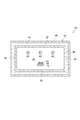
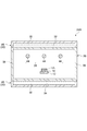
- FIG. 3 is a drawing for explaining a method for producing a functional layer.
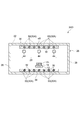
- FIG. 4 is a schematic diagram of a cross-sectional configuration along the line IV-IV of the infrared heating furnace shown in FIG.
- FIG. 5 is a schematic diagram for explaining a schematic configuration of the infrared heating furnace used in Examples 1 and 2.
- FIG. FIG. 6 is a schematic diagram for explaining a schematic configuration of a modified example of the infrared heating furnace.
- FIG. 7 is a schematic diagram for explaining a schematic configuration of another modified example of the infrared heating furnace.
- FIG. 8 is a schematic diagram for explaining a schematic configuration of still another modified example of the infrared heating furnace.
- An organic EL element 10 manufactured by a method for manufacturing an organic EL element (organic electronic element) according to an embodiment schematically illustrated in FIG. 1 is used as a light source of, for example, a curved or flat illumination device, for example, a scanner. It can be used for a planar light source and a display device.
- the organic EL element 10 includes a plastic substrate 12, an anode 14, an organic EL unit 16, and a cathode 18.
- the organic EL element 10 can take a form in which light is emitted from the anode 14 side or a form in which light is emitted from the cathode 18 side. Below, unless otherwise indicated, the form which radiate
- the plastic substrate 12 is transparent to visible light (light having a wavelength of 400 nm to 800 nm).
- the plastic substrate 12 has a film shape, for example, and has flexibility.
- the thickness of the plastic substrate 12 is, for example, 30 ⁇ m or more and 700 ⁇ m or less.
- plastic material examples include polyethersulfone (PES); polyester resins such as polyethylene terephthalate (PET) and polyethylene naphthalate (PEN); polyethylene (PE), polypropylene (PP), and cyclic polyolefin.
- PET polyethylene terephthalate
- PEN polyethylene naphthalate
- PE polyethylene
- PP polypropylene
- cyclic polyolefin Polyamide resin; Polycarbonate resin; Polystyrene resin; Polyvinyl alcohol resin; Saponified ethylene-vinyl acetate copolymer; Polyacrylonitrile resin; Acetal resin; Polyimide resin; Epoxy resin.
- a driving circuit for example, a circuit including a thin film transistor
- driving the organic EL element 10 may be formed on the plastic substrate 12.
- Such a drive circuit is usually made of a transparent material.
- a barrier film may be formed on the plastic substrate 12.
- the barrier film has a function of barriering moisture.
- the barrier film may have a function of blocking a gas (for example, oxygen).
- the barrier film can be, for example, a film made of silicon, oxygen, and carbon, or a film made of silicon, oxygen, carbon, and nitrogen.
- examples of the material of the barrier film are silicon oxide, silicon nitride, silicon oxynitride, and the like.
- An example of the thickness of the barrier film is 100 nm or more and 10 ⁇ m or less.
- the anode 14 is provided on the plastic substrate 12.
- the anode 14 is provided on the barrier film.
- an electrode having optical transparency is used.
- the electrode exhibiting light transmittance a thin film of metal oxide, metal sulfide, metal or the like having high electrical conductivity can be used, and a thin film having high light transmittance is preferably used.
- the anode 14 may have a network structure made of a conductor (for example, metal).
- Examples of the material of the anode 14 include indium oxide, zinc oxide, tin oxide, indium tin oxide (Indium Tin Oxide: abbreviated as ITO), indium zinc oxide (Indium Zinc Oxide: abbreviated as IZO), gold, platinum, silver, and copper. Among these, ITO, IZO, or tin oxide is preferable.
- the thickness of the anode 14 can be determined in consideration of light transmittance, electrical conductivity, and the like.
- the thickness of the anode 14 is usually 10 nm to 10 ⁇ m, preferably 20 nm to 1 ⁇ m, and more preferably 50 nm to 500 nm.
- the organic EL unit 16 is provided on the anode 14.
- the organic EL unit 16 is a functional unit that contributes to light emission of the organic EL element 10 such as charge transfer and charge recombination according to the voltage applied to the anode 14 and the cathode 18.
- the organic EL unit 16 includes a hole injection layer FL1, a hole transport layer FL2, a light emitting layer FL3, an electron transport layer FL4, and an electron injection layer FL5, and these are stacked bodies in order from the anode 14 side.
- the hole injection layer FL1, the hole transport layer FL2, the light emitting layer FL3, the electron transport layer FL4, and the electron injection layer FL5 are functional layers each having a predetermined function.
- the organic EL unit 16 is not limited to the exemplified one as long as it includes the light emitting layer FL3.
- the hole injection layer FL1 is provided on the anode 14 and has a function of improving the hole injection efficiency from the anode 14 to the light emitting layer FL3.
- the thickness of the hole injection layer FL1 varies as appropriate depending on the material used, and is set as appropriate so that the drive voltage and the light emission efficiency are appropriate.
- the thickness of the hole injection layer FL1 is, for example, 1 nm to 1 ⁇ m, preferably 2 nm to 500 nm, more preferably 5 nm to 200 nm.
- the material of the hole injection layer FL1 As the material of the hole injection layer FL1, a known hole injection material can be used.
- the hole injection material include oxides such as vanadium oxide, molybdenum oxide, ruthenium oxide, and aluminum oxide, polythiophene derivatives such as polyethylenedioxythiophene (PEDOT), phenylamine compounds, starburst amine compounds, phthalocyanine compounds, and amorphous materials. Examples include carbon and polyaniline.
- the hole transport layer FL2 is provided on the hole injection layer FL1, and injection of holes from the portion closer to the anode 14 in the anode 14, hole injection layer FL1, or hole transport layer FL2 into the light emitting layer FL3 is performed. It is a layer having a function of improving.
- the thickness of the hole transport layer FL2 varies as appropriate depending on the material used, and is appropriately set so that the drive voltage and the light emission efficiency have appropriate values.
- the thickness of the hole transport layer FL2 is, for example, 1 nm to 1 ⁇ m, preferably 2 nm to 500 nm, more preferably 5 nm to 200 nm.
- the material of the hole transport layer FL2 As the material of the hole transport layer FL2, a known hole transport material can be used.
- the material of the hole transport layer FL2 include polyvinyl carbazole or derivatives thereof, polysilane or derivatives thereof, polysiloxane or derivatives thereof having an aromatic amine in the side chain or main chain, pyrazoline or derivatives thereof, arylamine or derivatives thereof, Stilbene or derivatives thereof, triphenyldiamine or derivatives thereof, polyaniline or derivatives thereof, polythiophene or derivatives thereof, polyarylamine or derivatives thereof, polypyrrole or derivatives thereof, poly (p-phenylene vinylene) or derivatives thereof, or poly (2, 5-thienylene vinylene) or a derivative thereof.
- the material of the hole transport layer FL2 include a hole transport layer material disclosed in, for example, JP 2012-144722A.
- the light emitting layer FL3 is provided on the hole transport layer FL2, and the light emitting layer FL3 is a layer having a function of emitting light of a predetermined wavelength.
- the thickness of the light emitting layer FL3 varies depending on the material used, and is appropriately set so that the drive voltage and the light emission efficiency are appropriate values.
- the light emitting layer FL3 is usually formed of an organic substance that mainly emits fluorescence and / or phosphorescence, or an organic substance and a dopant that assists the organic substance.
- the dopant is added, for example, for improving luminous efficiency, changing the emission wavelength, and the like.
- the organic substance contained in the light emitting layer FL3 may be a low molecular compound or a high molecular compound.
- Examples of the light-emitting material constituting the light-emitting layer FL3 include the following dye-based materials, metal complex-based materials, polymer-based materials, and dopant materials.
- dye-based luminescent materials include cyclopentamine or derivatives thereof, tetraphenylbutadiene or derivatives thereof, triphenylamine or derivatives thereof, oxadiazole or derivatives thereof, pyrazoloquinoline or derivatives thereof, distyrylbenzene or derivatives thereof.
- Distyrylarylene or a derivative thereof pyrrole or a derivative thereof, thiophene ring compound, pyridine ring compound, perinone or a derivative thereof, perylene or a derivative thereof, oligothiophene or a derivative thereof, oxadiazole dimer or a derivative thereof, pyrazoline dimer or a derivative thereof Derivatives, quinacridone or derivatives thereof, coumarin or derivatives thereof, and the like.
- the metal complex-based light emitting material examples include rare earth metals such as Tb, Eu, and Dy, or Al, Zn, Be, Pt, Ir, and the like as a central metal, and oxadiazole, thiadiazole, phenylpyridine, and phenylbenzimidazole. And metal complexes having a quinoline structure or the like as a ligand.
- metal complexes include metal complexes having light emission from triplet excited states such as iridium complexes and platinum complexes, aluminum quinolinol complexes, benzoquinolinol beryllium complexes, benzoxazolyl zinc complexes, benzothiazole zinc complexes, azomethyl zinc complexes, A porphyrin zinc complex, a phenanthroline europium complex, etc. are mentioned.
- polymer light-emitting material examples include polyparaphenylene vinylene or derivatives thereof, polythiophene or derivatives thereof, polyparaphenylene or derivatives thereof, polysilane or derivatives thereof, polyacetylene or derivatives thereof, polyfluorene or derivatives thereof, polyvinylcarbazole or derivatives thereof.
- examples thereof include a material obtained by polymerizing at least one of a derivative, the dye material, and the metal complex material.
- dopant materials include perylene or derivatives thereof, coumarin or derivatives thereof, rubrene or derivatives thereof, quinacridone or derivatives thereof, squalium or derivatives thereof, porphyrin or derivatives thereof, styryl dyes, tetracene or derivatives thereof, pyrazolone or derivatives thereof, decacyclene Alternatively, derivatives thereof, phenoxazone or derivatives thereof, and the like can be given.
- the electron transport layer FL4 is provided on the light emitting layer FL3, and has a function of improving electron injection from the cathode 18, the electron injection layer FL5, or a portion of the electron transport layer FL4 closer to the cathode 18 to the light emitting layer FL3. It is a layer having.
- the thickness of the electron transport layer FL4 varies depending on the material used, and is appropriately set so that the drive voltage and the light emission efficiency are appropriate values.
- the thickness of the electron transport layer FL4 is, for example, 1 nm to 1 ⁇ m, preferably 2 nm to 500 nm, more preferably 5 nm to 200 nm.
- a known electron transport material can be used as the material of the electron transport layer FL4.
- the electron transport material constituting the electron transport layer FL4 include an oxadiazole derivative, anthraquinodimethane or a derivative thereof, benzoquinone or a derivative thereof, naphthoquinone or a derivative thereof, anthraquinone or a derivative thereof, tetracyanoanthraquinodimethane or a derivative thereof.
- the electron injection layer FL5 is a layer provided on the electron transport layer FL4 and having a function of improving the electron injection efficiency from the cathode 18 to the light emitting layer FL3.
- the thickness of the electron injection layer FL5 varies depending on the material used, and is appropriately set so that the drive voltage and the light emission efficiency are appropriate values.
- the thickness of the electron injection layer FL5 is, for example, 1 nm to 1 ⁇ m.
- a known electron injection material can be used as the material of the electron injection layer FL5.
- the material of the electron injection layer FL5 include alkali metals, alkaline earth metals, alloys containing at least one of alkali metals and alkaline earth metals, oxides of alkali metals or alkaline earth metals, halides, carbonic acids. Examples thereof include a salt or a mixture of these substances.
- alkali metal, alkali metal oxide, halide, and carbonate examples include lithium, sodium, potassium, rubidium, cesium, lithium oxide, lithium fluoride, sodium oxide, sodium fluoride, potassium oxide, potassium fluoride, and oxide.
- alkaline earth metal, alkaline earth metal oxide, halide and carbonate examples include magnesium, calcium, barium, strontium, magnesium oxide, magnesium fluoride, calcium oxide, calcium fluoride, barium oxide and barium fluoride. Strontium oxide, strontium fluoride, magnesium carbonate and the like.
- the electron injection layer FL5. a layer in which a conventionally known electron transporting organic material and an alkali metal organometallic complex are mixed can be used as the electron injection layer FL5.
- an ionic polymer compound containing an alkali metal salt in the side chain described in International Publication No. 12/133229 can also be used as the electron injection layer FL5.
- the cathode 18 is provided on the organic EL unit 16.
- the thickness of the cathode 18 varies depending on the material used, and is set in consideration of electrical conductivity, durability, and the like.
- the thickness of the cathode 18 is usually 10 nm to 10 ⁇ m, preferably 20 nm to 1 ⁇ m, and more preferably 50 nm to 500 nm.
- Examples of the material of the cathode 18 include alkali metals, alkaline earth metals, transition metals, and Group 13 metals of the periodic table.
- a transparent conductive electrode made of a conductive metal oxide, a conductive organic material, or the like may be used.
- the manufacturing method of the organic EL element 10 includes an anode forming step S10, an organic EL part forming step S12, and a cathode forming step S14.
- the anode 14 is formed on the plastic substrate 12.
- a plurality of organic EL element type regions are set in the longitudinal direction of the plastic substrate 12, and the anode 14 is formed in each organic EL element formation region.
- the anode 14 can be formed by a known method in the manufacture of an organic EL element. Examples of the method for forming the anode 14 include a vacuum deposition method, a sputtering method, an ion plating method, a plating method, and a coating method.
- an ink jet printing method can be mentioned, but other known coating methods may be used as long as the coating method can form the anode 14.
- Known coating methods other than the inkjet printing method include, for example, a micro gravure coating method, a gravure coating method, a bar coating method, a roll coating method, a wire bar coating method, a spray coating method, a screen printing method, a flexographic printing method, and an offset printing method. And a nozzle printing method.
- the solvent of the coating solution containing the material of the anode 14 may be any solvent that can dissolve the material of the anode 14.
- the solvent include chloride solvents such as chloroform, methylene chloride and dichloroethane, ether solvents such as tetrahydrofuran, aromatic hydrocarbon solvents such as toluene and xylene, ketone solvents such as acetone and methyl ethyl ketone, ethyl acetate, butyl acetate and ethyl cell.
- ester solvents such as sorb acetate.
- the organic EL part 16 is formed on the anode 14.
- the organic EL portion 16 is formed by sequentially stacking a hole injection layer FL1, a hole transport layer FL2, a light emitting layer FL3, an electron transport layer FL4, and an electron injection layer FL5 on the anode 14.
- FIG. 3 is a conceptual diagram of a method for forming the functional layer FL.
- FIG. 4 is a schematic diagram of a cross-sectional configuration along the line IV-IV of the infrared heating furnace shown in FIG.
- a layer already formed before the formation of the functional layer FL to be formed is illustrated as a base layer UL.
- the underlayer UL is, for example, the anode 14 for the hole injection layer FL1, the anode 14 and the hole injection layer FL1 for the hole transport layer FL2, and the anode 14 and the hole for the light emitting layer FL3.
- the underlayer UL for the electron transport layer FL4 and the electron injection layer FL5 is similarly defined.
- the method for forming the functional layer FL includes a coating film forming step and a heating step.
- the coating process and the heating process are sequentially performed while the belt-shaped plastic substrate 12 is transported by the transport roller R in the longitudinal direction (the direction of the white arrow in FIG. 3).
- a coating liquid L containing a material that becomes the functional layer FL is applied from the coating device 20 onto the plastic substrate 12 (specifically, on the base layer UL), A coating film 22 is formed.
- the coating device 20 may be any device according to a coating method (a method for coating a prepared coating solution).
- a slit coating method die coating method
- a micro gravure coating method a gravure coating method
- a bar coating method a roll coating method
- examples thereof include a wire bar coating method, a spray coating method, a screen printing method, a flexographic printing method, an offset printing method, an ink jet printing method, and a nozzle printing method.
- the coating method is an inkjet printing method
- the coating device 20 may be an inkjet device including an inkjet nozzle.
- the solvent of the coating liquid L containing the material of the functional layer FL may be any solvent that can dissolve the material of the functional layer FL.
- the solvent may be the same as the solvent mentioned in the description of the anode forming step S10.
- the coating liquid L may contain a crosslinkable group.
- the crosslinkable group may be included in the organic compound, or a crosslinker may be used as a material having a crosslinkable group.
- crosslinkable groups are vinyl, ethynyl, butenyl, acryloyl, acryloyloxyalkyl, acryloylamide, methacryloyl, methacryloyloxyalkyl, methacryloylamide, vinyl ether, vinylamino, silanol ,
- a group having a small ring for example, cyclopropane, cyclobutane, epoxide, oxetane, diketene, episulfide, etc.
- cyclopropyl group, cyclobutyl group, epoxy group, oxetane group, diketene group, episulfide group, three-membered ring or 4 Membered lactone groups, and 3-membered or 4-membered lactam groups for example, cyclopropane, cyclobutane, epoxide, oxetane, diketene, episulf
- crosslinking agent examples include vinyl group, ethynyl group, butenyl group, acryloyl group, acryloyloxyalkyl group, acryloylamide group, methacryloyl group, methacryloyloxyalkyl group, methacryloylamide group, vinyl ether group, vinylamino group, silanol group, Polymerizable from the group consisting of a cyclopropyl group, a cyclobutyl group, an epoxy group, an oxetane group, a diketene group, an episulfide group, a 3-membered or 4-membered lactone group, and a 3-membered or 4-membered lactam group
- the compound which has group can be mentioned.
- a polyfunctional acrylate is preferable, and examples thereof include dipentaerythritol hexaacrylate (DPHA) and trispentaerythritol octaacrylate (TPEA).
- DPHA dipentaerythritol hexaacrylate
- TPEA trispentaerythritol octaacrylate
- the coating film 22 formed on the plastic substrate 12 is carried into an infrared heating furnace 24 provided on the conveyance path as the plastic substrate 12 is conveyed.
- the coating film 22 is heated and cured in the infrared heating furnace 24 to form the functional layer FL.
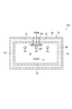
- the infrared heating furnace 24 used in the heating process will be described. As shown in FIGS. 3 and 4, the infrared heating furnace 24 includes a casing 26, an infrared irradiation unit 28, and a cooling mechanism 30.
- the housing 26 accommodates an infrared irradiation unit 28 and forms a heating space S for heat-treating the coating film 22.
- the housing 26 extends in the conveyance direction of the plastic substrate 12.
- the casing 26 has a box shape, and the top wall 32, the bottom wall 34, the side walls 36 and 38 (see FIG. 4) and the side walls 40 and 42 constituting the casing 26 function as a furnace wall of the infrared heating furnace 24.
- An example of the material of the top wall 32, the bottom wall 34, and the side walls 36, 38, 40, 42 is stainless steel (hereinafter also referred to as “SUS”).
- the top wall 32, the bottom wall 34, and the side walls 36 and 38 extend in the conveyance direction of the plastic substrate 12.
- the side wall 40 and the side wall 42 are substantially orthogonal to the conveyance direction of the plastic substrate 12.
- Each of the side wall 40 and the side wall 42 is formed with a carry-in port 40a and a carry-out port 42a through which the plastic substrate
- a gas supply port 26 a for supplying the inert gas G into the heating space S may be formed in the housing 26.
- the gas supply port 26 a can be formed, for example, in the vicinity of one end of the housing 26 in the transport direction of the plastic substrate 12.
- the gas supply port 26a is formed in the top wall 32, but the formation location of the gas supply port 26a is not limited to the location illustrated in FIG.
- An example of the inert gas is argon gas.
- casing 26 is provided in the housing
- the gas discharge port 26b is the other end of the housing 26 in the transport direction of the plastic substrate 12. It can be formed near the part.
- the inert gas G can flow in the longitudinal direction of the plastic substrate 12, and the plastic substrate 12 can be cooled with the inert gas G when the coating film 22 is heated.
- the gas exhaust port 26 b is formed in the top wall 32, but the formation location of the gas exhaust port 26 b is not limited to the location illustrated in FIG. 3.
- the casing 26 may be formed with a cooling air inlet for supplying cooling air into the heating space S.
- the infrared irradiation unit 28 has a plurality of infrared lamps 44.
- the infrared irradiation unit 28 includes three infrared lamps 44.
- Each infrared lamp 44 extends in the conveying direction of the plastic substrate 12, and the plurality of infrared lamps 44 are arranged in parallel.
- the infrared lamp 44 only needs to be disposed so as to be able to irradiate the coating film 22 with infrared IR.
- the infrared lamp 44 is disposed at a position facing the coating film 22. .
- the infrared lamp 44 normally emits infrared IR including a wavelength range of 1.2 ⁇ m to 10.0 ⁇ m.
- the infrared irradiation unit 28 exemplifies a form having a plurality of infrared lamps 44, but the infrared irradiation unit 28 may have at least one infrared lamp 44.
- the cooling mechanism 30 has a cooling jacket 46 provided in the housing 26 so as to surround the transport path of the plastic substrate 12, and cools the housing 26.
- the cooling jacket 46 is provided so as to cover the top wall 32, the bottom wall 34, and the side walls 36 and 38.
- the cooling jacket 46 extends in the conveyance direction of the plastic substrate 12.
- the cooling jacket 46 a space through which the cooling water W flows is formed.
- the cooling jacket 46 is a cooling water flow path for flowing the cooling water W supplied from the inlet 46a formed on one end side of the cooling jacket 46 toward the outlet 46b formed on the other end side. .
- the cooling jacket 46 is configured so that the cooling water W flows inside thereof, and a part of the casing 26 (in this embodiment, the top wall 32, the bottom wall 34, and the side walls 36 and 38) can be cooled by the cooling water W. Just do it.
- the cooling mechanism 30 may be a cooling water pipe provided in the top wall 32, the bottom wall 34, and the side walls 36, 38, or on the inner surface or the outer surface thereof.
- the inner surfaces of the top wall 32, the bottom wall 34, and the side walls 36 and 38 cooled by the cooling mechanism 30 are coated with an absorber that absorbs infrared rays having a wavelength range of 5.0 ⁇ m to 10.0 ⁇ m.
- the average absorptance of infrared rays having a wavelength range of 5.0 ⁇ m to 10.0 ⁇ m at the top wall 32, the bottom wall 34, and the side walls 36 and 38 may be 80% or more.
- the average absorption rate is obtained by dividing the energy absorption amount in the wavelength region by the irradiation energy in the wavelength region.
- the product of the infrared absorption rate and the infrared intensity at a specific wavelength is the energy absorption amount at the specific wavelength, and the energy absorption amount at the specific wavelength is defined as the energy absorption amount in the wavelength region.
- the top wall 32, the bottom wall 34, and the side walls 36 and 38 are made of a material having an average infrared absorption rate of 80% or more, coating is unnecessary.
- the heating process of the coating film 22 using the infrared heating furnace 24 will be described in more detail.
- the infrared irradiation unit 28 irradiates the coating film 22 with infrared IR. As a result, the coating film 22 is cured by heating to form the functional layer FL.
- the coating liquid L has a crosslinkable group
- a crosslinking reaction (including a polymerization reaction) occurs by heating the coating film 22 with infrared IR.
- the crosslinkable group is crosslinked, and the coating film 22 is cured to form the functional layer FL.
- the functional layer FL thus formed on the plastic substrate 12 is carried out from the carry-out port 42a.
- the conveyance speed of the plastic substrate 12 may be adjusted by infrared IR from the infrared irradiation unit 28 so that the coating film 22 is heated and cured to form the functional layer FL while passing through the infrared heating furnace 24. .
- the cooling water W is caused to flow into the cooling jacket 46 of the cooling mechanism 30, and more specifically, the inner surface of the housing 26, more specifically, the ceiling wall 32.
- the inner surfaces of the bottom wall 34 and the side walls 36 and 38 are cooled to 100 ° C. or lower.
- the temperature, flow rate, etc. of the cooling water W may be set so that the inner surfaces of the top wall 32, the bottom wall 34, and the side walls 36, 38 are 100 ° C. or lower.
- the inert gas G is supplied into the casing 26 from the gas supply port 26a, and the casing 26 is kept in an inert gas atmosphere.
- the inert gas G may be discharged from at least one of the plastic substrate 12 and the coating film 22 while discharging the inert gas G from the gas discharge port 26 b and flowing the inert gas G in the housing 26.
- the hole injection layer FL1, the hole transport layer FL2, the light emitting layer FL3, the electron transport layer FL4, and the electron injection layer FL5 are formed, by performing the formation method of the functional layer FL in order, It is formed on the anode 14. These can be carried out continuously while the plastic substrate 12 is transported in the longitudinal direction as shown in FIG.
- the cathode 18 is formed on the organic EL unit 16. Since the formation method of the cathode 18 can be the same as the formation method of the anode 14, the description thereof is omitted.
- the anode 14, the organic EL part 16, and the cathode 18 are provided in each of the plurality of organic EL element forming regions set on the belt-shaped plastic substrate 12, a cutting step is performed after the cathode forming step S14. And the organic EL element 10 is cut out. You may implement the sealing process which seals the organic EL element 10 with a sealing member before or after a cutting process.
- the plastic substrate 12 is unwound from the first roll (unwinding roll) on which the belt-shaped plastic substrate 12 is wound, and the second roll (winding up) It may be carried out in a roll-to-roll manner, which is carried out sequentially while being wound on a roll.
- the method for forming the functional layer FL shown in FIG. 3 corresponds to a partially enlarged view when the organic EL portion 16 is formed by the roll-to-roll method.
- Any of the anode forming step S10, the organic EL portion forming step S12, and the cathode forming step S14 may be performed by a roll-to-roll method.
- the hole injection layer FL1, the hole transport layer FL2, the light emitting layer FL3, and the like are referred to as a functional layer FL.
- the functional layers FL such as the hole injection layer FL1, the hole transport layer FL2, and the light emitting layer FL3 constituting the organic EL portion 16 are formed by a coating method. That is, after the coating film 22 is formed on the plastic substrate 12, the coating film 22 is heated and cured with infrared IR to form the functional layer FL.
- the coating method is employed for forming the functional layer FL, as illustrated in FIG. 3, the coating film forming step and the heating step can be continuously performed while the plastic substrate 12 is being conveyed.
- the functional layer FL included in the organic EL unit 16 usually has an absorption peak in the wavelength range of 1.2 ⁇ m to 5.0 ⁇ m of the infrared IR, and the wavelength range of 5.0 ⁇ m to 10. It tends to absorb more infrared rays having a wavelength range of 1.2 ⁇ m to 5.0 ⁇ m than 0 ⁇ m infrared rays.
- the coating film 22 can be efficiently heated, so that the heating process time can be shortened. As a result, the productivity of the organic EL element 10 is improved.
- Infrared rays with a wavelength range of 1.2 ⁇ m to 5.0 ⁇ m correspond to near infrared rays
- infrared rays with a wavelength range of 5.0 ⁇ m to 10.0 ⁇ m correspond to far infrared rays.
- Infrared rays and infrared rays having a wavelength range of 5.0 ⁇ m to 10.0 ⁇ m are sometimes simply referred to as near infrared rays and far infrared rays, respectively.
- a part of the casing 26 that is a member of the infrared heating furnace 24, that is, the top wall 32, the bottom wall 34, and the side walls 36 It is important that 38 is cooled to 100 ° C. or lower. This point will be described in comparison with a case where a part of the casing 26 is not cooled.
- the infrared IR is emitted radially from the infrared lamp 44 included in the infrared irradiation unit 28, the infrared IR emitted from the infrared lamp 44 also enters the casing 26 in addition to the coating film 22.
- the temperature of the casing 26 rises.
- far infrared radiation is generated from the inner surface of the housing 26, and far infrared light from the housing 26 enters the plastic substrate 12.
- the plastic material that is the material of the plastic substrate 12 hardly absorbs near infrared rays, and has an absorption characteristic of absorbing far infrared rays more.
- the plastic material has an absorption characteristic that, in the absorption spectrum of the plastic material, the integrated value in the wavelength range of 1.2 ⁇ m to 5.0 ⁇ m is smaller than the integrated value in the wavelength range of 5.0 ⁇ m to 10 ⁇ m.
- the far-infrared radiation is generated from the casing 26, the far-infrared radiation is absorbed by the plastic substrate 12, and the temperature of the plastic substrate 12 rises unnecessarily.
- the temperature of the plastic substrate 12 rises, for example, when the glass substrate temperature is higher than the glass transition temperature, the plastic substrate 12 is deformed, so that the post-process cannot be performed, or the defective rate of the manufactured organic EL elements increases. As a result, the manufacturing yield decreases.
- the conveyance roller R contacting the plastic substrate 12 is cooled, or a metal belt conveyor having a high thermal conductivity is used for conveying the plastic substrate 12. It is also possible. However, the plastic substrate 12 is not cooled between the transport roller R and the transport roller R or at the joint of the belt conveyor. Therefore, the heating state of the coating film 22 becomes non-uniform through the plastic substrate 12, and as a result, the cured state of the coating film 22 tends to be non-uniform. Thereby, a post-process cannot be implemented or the defective product rate of the manufactured organic EL element increases, and the manufacturing yield of the organic EL element decreases.
- a part of the casing 26 that is a member of the infrared heating furnace 24, that is, the top wall 32, the bottom wall 34, and the side walls 36 and 38 are removed. It is cooled to 100 ° C or lower. Since the top wall 32, the bottom wall 34, and the side walls 36 and 38 surround the periphery of the plastic substrate 12 in a tunnel shape, when the coating film 22 is heated by infrared irradiation, the plastic substrate 12 is surrounded by the periphery of the plastic substrate 12. A cooling region cooled to 100 ° C. or less in a tunnel shape is formed at a distant position.
- the amount of far infrared rays incident on the plastic substrate 12 can be reduced to 1/3 or less of the amount of near infrared rays incident on the plastic substrate 12. Therefore, the temperature rise of the plastic substrate 12 is suppressed, and damage such as deformation of the plastic substrate 12 is prevented. Therefore, the manufacturing yield of the organic EL element 10 can be improved.
- the plastic substrate 12 is cooled by the inert gas G, and thus the temperature rise of the plastic substrate 12 is further suppressed. Is done. As described above, even if the inert gas G is used to cool the plastic substrate 12, if the top wall 32, the bottom wall 34, and the side walls 36 and 38 are cooled to 100 ° C. or lower, the top wall 32 and the like are removed. Since the amount of the inert gas G can be reduced as compared with the case where it is not cooled below 100 ° C., the manufacturing cost of the organic EL element 10 can be reduced.
- the top wall 32, the bottom wall 34, and the side walls 36 and 38 cooled by the cooling mechanism 30 are arranged away from the plastic substrate 12. Therefore, the coating film 22 is uniformly cured without the occurrence of non-uniformity in the heating state of the coating film 22 as in the case of cooling the transport roller R contacting the plastic substrate 12 or using a metallic belt conveyor. it can. Also from this viewpoint, the production yield of the organic EL element 10 can be improved.
- the far-infrared absorptivity of the top wall 32, the bottom wall 34, and the side walls 36, 38 cooled to 100 ° C. or less is 80% or more
- the far-infrared rays in the casing 26 are absorbed by them.
- the amount of far infrared rays in the body 26 can be greatly reduced.
- the far-infrared absorptivity of the top wall 32, the bottom wall 34, and the side walls 36, 38 is 80% or more.
- By coating it means that the far-infrared absorptivity of the top wall 32, the bottom wall 34, and the side walls 36 and 38 is 80% or more.
- a substrate having a size of 24 mm ⁇ 24 mm ⁇ 0.7 mm was used as the plastic substrate 12.
- the material of the plastic substrate 12 was PEN, and the glass transition temperature was 155 ° C.
- the plastic substrate 12 was heated in the infrared heating furnace 24A shown in FIG.
- the infrared heating furnace 24 ⁇ / b> A was provided with a box-shaped casing 26, three infrared lamps 44, and a cooling mechanism 30.
- the material of the casing 26 was SUS.
- the casing 26 is formed with a cooling air introduction port 26c, and the cooling air diffusion plate DP is disposed at a position away from the cooling air introduction port 26c so as to face the cooling air introduction port 26c.
- the cooling air diffusion plate DP was disposed between the cooling air introduction port 26 c and the infrared lamp 44.
- the material of the cooling air diffusion plate DP was SUS.
- the three infrared lamps 44 were disposed in the casing 26 so as to face the plastic substrate 12.
- the distance between the infrared lamp 44 and the plastic substrate 12 was 150 mm.
- the distance between the infrared lamp 44 and the plastic substrate 12 is a distance between a plane including the centers of the three infrared lamps 44 and the plastic substrate 12.
- Infrared IR including a wavelength range of 1.2 ⁇ m to 10.0 ⁇ m was emitted from the infrared lamp 44.
- a cooling jacket 46 is adopted for the cooling mechanism 30.
- the cooling jacket 46 is configured such that the cooling water W flows in the cooling jacket 46, and the cooling jacket 46 covers the entire area of the outer surface of the casing 26 other than the cooling air inlet.
- Example 1 In Example 1, by supplying 500 W of power to the infrared lamp 44, the infrared IR was applied to the plastic substrate 12 from the infrared lamp 44 for 10 minutes, and the plastic substrate 12 was heated. During this heating, 17 ° C. cooling water W was allowed to flow into the cooling jacket 46. Further, air was supplied as cooling air from the cooling air inlet 26c into the housing 26 at a flow rate of 50 L / min.
- the wall surface temperature of the casing 26, the temperature of the infrared lamp 44 (lamp temperature), and the temperature of the plastic substrate 12 (substrate temperature) are measured. As shown, they were 52 ° C, 200 ° C, and 153 ° C, respectively.
- the incident amount of near infrared rays and the incident amount of far infrared rays to the plastic substrate 12 were calculated by simulation using the Monte Carlo method. As a result, as shown in Table 1, the incident amount of near infrared rays was 7.8 kw / m 2 , and the incident amount of near infrared rays was 2.4 kw / m 2 .
- Example 2 In Example 2, a heating experiment of the plastic substrate 12 was performed under the same conditions as in Example 1 except that the cooling air was not supplied to the casing 26 from the cooling air inlet 26c.
- the wall surface temperature of the casing 26, the temperature of the infrared lamp 44 (lamp temperature), and the temperature of the plastic substrate 12 (substrate temperature) were measured, as shown in Table 1 above, they were 54 ° C, 200 ° C, and 153 ° C, respectively. there were.
- the incident amount of near infrared rays and the incident amount of far infrared rays to the plastic substrate 12 were calculated by simulation using the Monte Carlo method, as in the case of Example 1.
- the incident amount of near infrared rays was 7.8 kw / m 2
- the incident amount of near infrared rays was 2.4 kw / m 2 .
- the wall surface temperature can be cooled to 100 ° C. or lower by cooling the casing 26 with the cooling jacket.
- the temperature of the plastic substrate 12 can be suppressed to about 153 ° C. which is lower than the glass transition temperature of PEN which is the material of the plastic substrate 12.
- the incident amount of the far-infrared plastic substrate 12 can be reduced to one third or less of the incident amount of the near-infrared ray.
- the top wall 32, the bottom wall 34, and the side walls 36 and 38 of the housing 26 are covered with a cooling jacket 46 of the cooling mechanism 30, and a cooling region is formed in a tunnel shape around the transport path of the plastic substrate 12. Formed.
- the cooling jacket 46 constituting the cooling mechanism 30 is provided on the top wall 32 and the bottom wall 34 positioned on the upper side and the lower side in the thickness direction of the plastic substrate 12.
- the top wall 32 and the bottom wall 34 may be cooled to 100 ° C. or lower.
- the plastic substrate 12 used for the organic EL element usually have a larger area than the side surface of the plastic substrate 12. Therefore, if at least the top wall 32 and the bottom wall 34 are cooled to 100 ° C. or lower and far-infrared radiation from them is suppressed, incidence of far-infrared rays on the plastic substrate 12 can be easily reduced.
- top wall 32 and the bottom wall 34 are cooled by the cooling mechanism 30 is illustrated as a modified example, but a part of the housing 26 may be cooled by the cooling mechanism 30 to 100 ° C. or less.
- the cooling member 48 is disposed between the housing 26 and the plastic substrate 12, and the cooling member 48 is cooled by the cooling mechanism 30 ⁇ / b> A. It may be formed.
- a tunnel-shaped (or cylindrical) cooling member 48 formed so as to surround the plastic substrate 12 is illustrated.
- the cooling member 48 extends in the conveyance direction of the plastic substrate 12.
- the cross-sectional shape of the cooling member 48 perpendicular to the conveying direction of the plastic substrate 12 may be a quadrangular shape (a square shape, a rectangular shape, etc.) or a circular shape as shown in FIG.
- the material of the cooling member 48 is SUS, iron, ceramic, or the like.
- the cooling mechanism 30 ⁇ / b> A may be disposed in the cooling member 48 and have a pipe 50 for flowing the cooling water W.
- the pipe 50 may be attached to the outer surface or the inner surface of the cooling member 48.
- the cooling member 48 when the coating film 22 is heated with infrared IR, the cooling member 48 is cooled to 100 ° C. or less by the cooling mechanism 30A.
- the cooling member 48 surrounds the plastic substrate 12, and the infrared irradiation unit 28 is also disposed inside the cooling member 48. Therefore, most of the infrared IR irradiated from the infrared irradiation unit 28 toward the inner surface of the housing 26 is blocked by the cooling member 48. Therefore, far-infrared radiation from the inner surface of the casing 26 caused by the infrared IR hardly enters the plastic substrate 12. Since the cooling member 48 is also cooled to 100 ° C. or lower, far-infrared radiation from the cooling member 48 does not occur. Therefore, the coating film 22 can be heated with infrared IR while suppressing damage to the plastic substrate 12 in the heating process.
- a part of the casing 26 may be further cooled to 100 ° C. or less by a cooling mechanism.
- the tunnel-like cooling member 48 is exemplified. However, like the infrared heating furnace 24D shown in FIG. 8, a plate-like cooling member 48 is provided at a position away from the plastic substrate 12 in a part of the periphery of the plastic substrate 12. The cooling member 48 may be disposed and the cooling member 48 may be cooled by the cooling mechanism 30A. In the third modification, as in the second modification, the cooling member 48 extends in the conveyance direction of the plastic substrate 12. An example of the cooling mechanism 30A is the same as that of the second modification. The plate-like cooling member 48 may be provided on a part of the periphery of the plastic substrate 12, but as shown in FIG. 8, the cooling member 48 is provided on at least the upper side and the lower side of the plastic substrate 12, respectively. By cooling them to 100 ° C. or lower, it is easy to suppress the temperature rise of the plastic substrate 12 due to far infrared rays.
- a part of the housing 26 may be further cooled to 100 ° C. or less by a cooling mechanism.
- the cooling member 48 may be made of a material having an average far-infrared absorptance of 80% or more, or at least of the cooling member 48.
- the surface of the plastic substrate 12 may be coated with an absorbing agent that absorbs far infrared rays, and the average far infrared absorption rate of the cooling member 48 may be 80% or more.
- the member of the infrared heating furnace for example, a part of the casing, a cooling member, etc.
- the cooling region formed by cooling the substrate to 100 ° C. or lower may be formed in part in the transport direction of the plastic substrate.
- a plurality of the cooling regions may be formed discretely in the transport direction. For example, even if a plurality of cooling regions are discretely formed in the plastic substrate transport direction, the joint between the adjacent cooling regions and the cooling regions and the plastic substrate 12 are separated from each other. It is hard to make a difference in
- Water was exemplified as the refrigerant used by the cooling mechanism.
- the refrigerant is not limited to water, and for example, cooled air, antifreeze, or the like may be used.
- the cooling mechanism may not use a refrigerant, and for example, a Peltier element or the like may be used.
- the organic EL portion may be a laminate including a functional layer other than the light emitting layer.
- Examples of the layer configuration of the organic EL element including various functional layers are shown below.
- the configuration of the organic EL element shown in FIG. 1 corresponds to the following configuration (g).
- Anode / light emitting layer / cathode (b) Anode / hole injection layer / light emitting layer / cathode (c) Anode / hole injection layer / light emitting layer / electron injection layer / cathode (d) Anode / hole injection layer / Light emitting layer / electron transport layer / electron injection layer / cathode (e) anode / hole injection layer / hole transport layer / light emitting layer / cathode (f) anode / hole injection layer / hole transport layer / light emitting layer / Electron injection layer / cathode (g) anode / hole injection layer / hole transport layer / light emitting layer / electron transport layer / electron injection layer / cathode (h) anode / light emitting layer / electron injection layer / cathode (i) anode / Light emitting layer / electron transport layer / electron injection layer / cathode The symbol
- these layers may be referred to as an electron block layer.
- these layers may be referred to as a hole blocking layer.
- the organic EL element may have a single light emitting layer or two or more light emitting layers.
- the organic EL when the stacked structure disposed between the anode and the cathode is “structural unit I”, the organic EL having two light emitting layers
- the layer structure shown to the following (j) can be mentioned, for example.
- the two (structural units I) may have the same or different layer structure.
- the charge generation layer is a layer that generates holes and electrons by applying an electric field.
- Examples of the charge generation layer include a thin film made of vanadium oxide, ITO, molybdenum oxide, or the like.
- Examples of the configuration of the organic EL element having three or more light-emitting layers include the layer configuration shown in the following (k). it can.
- (Structural Unit II) x represents a stacked body in which (Structural Unit II) is stacked in x stages.
- a plurality of (structural units II) may have the same or different layer structure.
- An organic EL element may be configured by directly laminating a plurality of light emitting layers without providing a charge generation layer.
- the electrode formed on the plastic substrate 12 has been described as an anode, a cathode may be provided on the plastic substrate side.
- the manufacturing method of the organic electronic element which has an organic functional layer is not limited to the exemplified organic EL element, but is a predetermined method such as an organic transistor (organic electronic element), an organic photoelectric conversion element (organic electronic element), and an organic solar cell (organic electronic element). It can apply to the manufacturing method of the organic electronic element which has these functional layers.
- SYMBOLS 10 Organic EL element (organic electronic element), 22 ... Coating film, 24, 24A, 24B, 24C, 24D ... Infrared heating furnace, 26 ... Housing
Landscapes
- Engineering & Computer Science (AREA)
- Manufacturing & Machinery (AREA)
- Physics & Mathematics (AREA)
- Electromagnetism (AREA)
- Optics & Photonics (AREA)
- Electroluminescent Light Sources (AREA)
- Application Of Or Painting With Fluid Materials (AREA)
Priority Applications (4)
| Application Number | Priority Date | Filing Date | Title |
|---|---|---|---|
| US16/309,727 US10833273B2 (en) | 2016-06-17 | 2017-06-14 | Method for manufacturing organic element and method for producing function layer each using infrared rays to heat and cure coating film |
| EP17813349.2A EP3474634A4 (en) | 2016-06-17 | 2017-06-14 | METHOD FOR PRODUCING AN ORGANIC ELECTRONIC ELEMENT AND METHOD FOR PRODUCING A FUNCTIONAL LAYER |
| KR1020197000856A KR20190018476A (ko) | 2016-06-17 | 2017-06-14 | 유기 전자 소자의 제조 방법 및 기능층의 제조 방법 |
| CN201780037336.7A CN109315044B (zh) | 2016-06-17 | 2017-06-14 | 有机电子元件的制造方法及功能层的制造方法 |
Applications Claiming Priority (2)
| Application Number | Priority Date | Filing Date | Title |
|---|---|---|---|
| JP2016121010A JP6440654B2 (ja) | 2016-06-17 | 2016-06-17 | 有機電子素子の製造方法及び機能層の製造方法 |
| JP2016-121010 | 2016-06-17 |
Publications (1)
| Publication Number | Publication Date |
|---|---|
| WO2017217454A1 true WO2017217454A1 (ja) | 2017-12-21 |
Family
ID=60663127
Family Applications (1)
| Application Number | Title | Priority Date | Filing Date |
|---|---|---|---|
| PCT/JP2017/021966 WO2017217454A1 (ja) | 2016-06-17 | 2017-06-14 | 有機電子素子の製造方法及び機能層の製造方法 |
Country Status (6)
Cited By (2)
| Publication number | Priority date | Publication date | Assignee | Title |
|---|---|---|---|---|
| CN112514536A (zh) * | 2018-07-23 | 2021-03-16 | 住友化学株式会社 | 有机电子器件的制造方法 |
| US20210273171A1 (en) * | 2018-06-25 | 2021-09-02 | Sumitomo Chemical Company, Limited | Manufacturing method for functional film, drying device, and manufacturing device for functional film |
Families Citing this family (2)
| Publication number | Priority date | Publication date | Assignee | Title |
|---|---|---|---|---|
| JP2020021707A (ja) * | 2018-08-03 | 2020-02-06 | 住友化学株式会社 | 近赤外線と遠赤外線を併用する有機電子素子の製造方法及び有機電子素子の製造装置 |
| WO2020197753A1 (en) * | 2019-03-25 | 2020-10-01 | Sinovia Technologies | Non-equilibrium thermal curing processes |
Citations (6)
| Publication number | Priority date | Publication date | Assignee | Title |
|---|---|---|---|---|
| JP2003194467A (ja) * | 2001-12-25 | 2003-07-09 | Showa Mfg Co Ltd | 均熱処理装置 |
| JP2005081697A (ja) * | 2003-09-09 | 2005-03-31 | Toyo Ink Mfg Co Ltd | ガスバリア性積層体の製造方法 |
| JP2006085933A (ja) * | 2004-09-14 | 2006-03-30 | Toshiba Matsushita Display Technology Co Ltd | 表示装置の製造方法及び製造装置 |
| JP2006100134A (ja) * | 2004-09-29 | 2006-04-13 | Fuji Electric Holdings Co Ltd | 色変換フィルタ基板およびそれを用いた有機el素子の製造方法 |
| JP2008226642A (ja) * | 2007-03-13 | 2008-09-25 | Toppan Printing Co Ltd | 有機機能性薄膜熱処理装置および有機機能性素子の製造方法 |
| WO2013180036A1 (ja) * | 2012-05-28 | 2013-12-05 | 三菱化学株式会社 | 導電性薄膜積層体の製造方法 |
Family Cites Families (10)
| Publication number | Priority date | Publication date | Assignee | Title |
|---|---|---|---|---|
| US5092059A (en) * | 1988-06-07 | 1992-03-03 | W. R. Grace & Co.-Conn. | Infrared air float bar |
| JP4244382B2 (ja) * | 2003-02-26 | 2009-03-25 | セイコーエプソン株式会社 | 機能性材料定着方法及びデバイス製造方法 |
| US20050124258A1 (en) * | 2003-12-08 | 2005-06-09 | E-Lite Technologies, Inc. | Electroluminescent lamp construction and electroluminescent lamp made thereby |
| JP4092593B2 (ja) * | 2006-05-18 | 2008-05-28 | 富士フイルム株式会社 | 被乾燥物の乾燥方法及び装置 |
| US10422578B2 (en) * | 2010-04-08 | 2019-09-24 | Ncc Nano, Pllc | Apparatus for curing thin films on a moving substrate |
| CN103442870B (zh) * | 2011-03-25 | 2015-11-25 | 宇部兴产株式会社 | 聚酰亚胺膜的制备方法、聚酰亚胺膜的制备装置及聚酰亚胺膜 |
| US9855769B2 (en) * | 2011-07-01 | 2018-01-02 | Hewlett-Packard Development Company, L.P. | Curing apparatus, image forming apparatus, and articles of manufacture |
| CN103328115A (zh) | 2012-01-23 | 2013-09-25 | 日本碍子株式会社 | 形成于pet膜表面的涂膜的干燥方法及涂膜干燥炉 |
| US9750091B2 (en) * | 2012-10-15 | 2017-08-29 | Applied Materials, Inc. | Apparatus and method for heat treatment of coatings on substrates |
| KR101692182B1 (ko) | 2013-06-18 | 2017-01-02 | 코니카 미놀타 가부시키가이샤 | 유기 발광 소자 |
-
2016
- 2016-06-17 JP JP2016121010A patent/JP6440654B2/ja not_active Expired - Fee Related
-
2017
- 2017-06-14 CN CN201780037336.7A patent/CN109315044B/zh not_active Expired - Fee Related
- 2017-06-14 WO PCT/JP2017/021966 patent/WO2017217454A1/ja unknown
- 2017-06-14 KR KR1020197000856A patent/KR20190018476A/ko not_active Ceased
- 2017-06-14 EP EP17813349.2A patent/EP3474634A4/en not_active Withdrawn
- 2017-06-14 US US16/309,727 patent/US10833273B2/en not_active Expired - Fee Related
Patent Citations (6)
| Publication number | Priority date | Publication date | Assignee | Title |
|---|---|---|---|---|
| JP2003194467A (ja) * | 2001-12-25 | 2003-07-09 | Showa Mfg Co Ltd | 均熱処理装置 |
| JP2005081697A (ja) * | 2003-09-09 | 2005-03-31 | Toyo Ink Mfg Co Ltd | ガスバリア性積層体の製造方法 |
| JP2006085933A (ja) * | 2004-09-14 | 2006-03-30 | Toshiba Matsushita Display Technology Co Ltd | 表示装置の製造方法及び製造装置 |
| JP2006100134A (ja) * | 2004-09-29 | 2006-04-13 | Fuji Electric Holdings Co Ltd | 色変換フィルタ基板およびそれを用いた有機el素子の製造方法 |
| JP2008226642A (ja) * | 2007-03-13 | 2008-09-25 | Toppan Printing Co Ltd | 有機機能性薄膜熱処理装置および有機機能性素子の製造方法 |
| WO2013180036A1 (ja) * | 2012-05-28 | 2013-12-05 | 三菱化学株式会社 | 導電性薄膜積層体の製造方法 |
Non-Patent Citations (1)
| Title |
|---|
| See also references of EP3474634A4 * |
Cited By (3)
| Publication number | Priority date | Publication date | Assignee | Title |
|---|---|---|---|---|
| US20210273171A1 (en) * | 2018-06-25 | 2021-09-02 | Sumitomo Chemical Company, Limited | Manufacturing method for functional film, drying device, and manufacturing device for functional film |
| CN112514536A (zh) * | 2018-07-23 | 2021-03-16 | 住友化学株式会社 | 有机电子器件的制造方法 |
| EP3829267A4 (en) * | 2018-07-23 | 2022-04-20 | Sumitomo Chemical Company Limited | Method for manufacturing organic electronic device |
Also Published As
| Publication number | Publication date |
|---|---|
| JP2017224573A (ja) | 2017-12-21 |
| KR20190018476A (ko) | 2019-02-22 |
| CN109315044A (zh) | 2019-02-05 |
| EP3474634A4 (en) | 2020-02-19 |
| US10833273B2 (en) | 2020-11-10 |
| US20190140180A1 (en) | 2019-05-09 |
| JP6440654B2 (ja) | 2018-12-19 |
| CN109315044B (zh) | 2021-01-12 |
| EP3474634A1 (en) | 2019-04-24 |
Similar Documents
| Publication | Publication Date | Title |
|---|---|---|
| JP6440654B2 (ja) | 有機電子素子の製造方法及び機能層の製造方法 | |
| JP6079936B1 (ja) | 有機el素子の製造方法 | |
| WO2020027149A1 (ja) | 近赤外線と遠赤外線を併用する有機電子素子の製造方法及び有機電子素子の製造装置 | |
| JP6079937B1 (ja) | 有機el素子の製造方法 | |
| JP7250633B2 (ja) | 有機elデバイスの製造方法 | |
| WO2021005976A1 (ja) | 有機電子デバイスの製造方法 | |
| JP6061057B1 (ja) | 有機el素子の製造方法 | |
| JP2021005469A (ja) | 有機電子デバイスの製造方法 | |
| JP6781568B2 (ja) | 有機電子デバイスの製造方法 | |
| JP6875842B2 (ja) | 有機電子デバイスの製造方法、電極付き基板及び有機電子デバイス | |
| US20210265567A1 (en) | Method for manufacturing organic electronic device | |
| WO2020090831A1 (ja) | 電子デバイスの製造方法 | |
| JP2017212143A (ja) | 有機電子デバイスの製造方法 | |
| US10510994B2 (en) | Method for manufacturing organic device, and roll | |
| JP2019003943A (ja) | 有機電子デバイスの製造方法 | |
| WO2018230602A1 (ja) | 有機電子デバイスの製造方法 | |
| JP2020167023A (ja) | 有機elデバイス用隔壁付基板の製造方法及び有機elデバイスの製造方法 | |
| JP2005332633A (ja) | 有機エレクトロルミネッセンス表示装置 | |
| JP2017004951A (ja) | 有機el素子の製造方法 | |
| JP2017004953A (ja) | 有機el素子の製造方法 | |
| JP2017004954A (ja) | 有機el素子の製造方法 | |
| JP2017004950A (ja) | 有機el素子の製造方法 | |
| JP2017004952A (ja) | 有機el素子の製造方法 | |
| JP2014232632A (ja) | 電子デバイスの製造方法 |
Legal Events
| Date | Code | Title | Description |
|---|---|---|---|
| 121 | Ep: the epo has been informed by wipo that ep was designated in this application |
Ref document number: 17813349 Country of ref document: EP Kind code of ref document: A1 |
|
| NENP | Non-entry into the national phase |
Ref country code: DE |
|
| ENP | Entry into the national phase |
Ref document number: 20197000856 Country of ref document: KR Kind code of ref document: A |
|
| ENP | Entry into the national phase |
Ref document number: 2017813349 Country of ref document: EP Effective date: 20190117 |