WO2017217308A1 - Composant électronique, plaque vibrante, dispositif électronique et procédé de fabrication de composants électroniques - Google Patents
Composant électronique, plaque vibrante, dispositif électronique et procédé de fabrication de composants électroniques Download PDFInfo
- Publication number
- WO2017217308A1 WO2017217308A1 PCT/JP2017/021254 JP2017021254W WO2017217308A1 WO 2017217308 A1 WO2017217308 A1 WO 2017217308A1 JP 2017021254 W JP2017021254 W JP 2017021254W WO 2017217308 A1 WO2017217308 A1 WO 2017217308A1
- Authority
- WO
- WIPO (PCT)
- Prior art keywords
- main surface
- insulating base
- base material
- insulating
- coil
- Prior art date
Links
- 238000004519 manufacturing process Methods 0.000 title claims description 33
- 238000000034 method Methods 0.000 title claims description 29
- 239000004020 conductor Substances 0.000 claims abstract description 234
- 239000000758 substrate Substances 0.000 claims abstract description 83
- 238000010030 laminating Methods 0.000 claims abstract description 20
- 238000004804 winding Methods 0.000 claims abstract description 13
- 238000009413 insulation Methods 0.000 claims abstract description 11
- 239000000463 material Substances 0.000 claims description 433
- 230000008569 process Effects 0.000 claims description 19
- 229920005992 thermoplastic resin Polymers 0.000 claims description 16
- 230000015572 biosynthetic process Effects 0.000 claims description 12
- 238000010438 heat treatment Methods 0.000 claims description 11
- 238000003825 pressing Methods 0.000 claims description 7
- 238000003475 lamination Methods 0.000 abstract 1
- 239000010410 layer Substances 0.000 description 172
- 239000011229 interlayer Substances 0.000 description 22
- 230000000694 effects Effects 0.000 description 20
- 229920000106 Liquid crystal polymer Polymers 0.000 description 10
- 239000004977 Liquid-crystal polymers (LCPs) Substances 0.000 description 10
- 238000000926 separation method Methods 0.000 description 10
- 238000005304 joining Methods 0.000 description 8
- RYGMFSIKBFXOCR-UHFFFAOYSA-N Copper Chemical compound [Cu] RYGMFSIKBFXOCR-UHFFFAOYSA-N 0.000 description 7
- 229920001187 thermosetting polymer Polymers 0.000 description 7
- 230000000052 comparative effect Effects 0.000 description 6
- 239000011888 foil Substances 0.000 description 6
- 239000002184 metal Substances 0.000 description 6
- 229910052751 metal Inorganic materials 0.000 description 6
- 239000012141 concentrate Substances 0.000 description 4
- 229910000679 solder Inorganic materials 0.000 description 4
- 239000004696 Poly ether ether ketone Substances 0.000 description 3
- 239000000853 adhesive Substances 0.000 description 3
- 230000001070 adhesive effect Effects 0.000 description 3
- 239000003990 capacitor Substances 0.000 description 3
- 238000002844 melting Methods 0.000 description 3
- 230000008018 melting Effects 0.000 description 3
- 238000000059 patterning Methods 0.000 description 3
- 238000000206 photolithography Methods 0.000 description 3
- 229920002530 polyetherether ketone Polymers 0.000 description 3
- 229920005989 resin Polymers 0.000 description 3
- 239000011347 resin Substances 0.000 description 3
- 239000004593 Epoxy Substances 0.000 description 2
- 230000008859 change Effects 0.000 description 2
- 230000004907 flux Effects 0.000 description 2
- 230000012447 hatching Effects 0.000 description 2
- 230000001678 irradiating effect Effects 0.000 description 2
- 238000012986 modification Methods 0.000 description 2
- 230000004048 modification Effects 0.000 description 2
- 230000000704 physical effect Effects 0.000 description 2
- 238000004026 adhesive bonding Methods 0.000 description 1
- 239000012790 adhesive layer Substances 0.000 description 1
- 229910045601 alloy Inorganic materials 0.000 description 1
- 239000000956 alloy Substances 0.000 description 1
- 239000000919 ceramic Substances 0.000 description 1
- 239000003795 chemical substances by application Substances 0.000 description 1
- 229910052802 copper Inorganic materials 0.000 description 1
- 230000007423 decrease Effects 0.000 description 1
- 238000006073 displacement reaction Methods 0.000 description 1
- 239000011521 glass Substances 0.000 description 1
- 229910052750 molybdenum Inorganic materials 0.000 description 1
- 229910052759 nickel Inorganic materials 0.000 description 1
- 230000002093 peripheral effect Effects 0.000 description 1
- 229910052709 silver Inorganic materials 0.000 description 1
- 229910052718 tin Inorganic materials 0.000 description 1
Images


Classifications
-
- H—ELECTRICITY
- H01—ELECTRIC ELEMENTS
- H01F—MAGNETS; INDUCTANCES; TRANSFORMERS; SELECTION OF MATERIALS FOR THEIR MAGNETIC PROPERTIES
- H01F17/00—Fixed inductances of the signal type
- H01F17/0006—Printed inductances
-
- H—ELECTRICITY
- H01—ELECTRIC ELEMENTS
- H01F—MAGNETS; INDUCTANCES; TRANSFORMERS; SELECTION OF MATERIALS FOR THEIR MAGNETIC PROPERTIES
- H01F17/00—Fixed inductances of the signal type
- H01F17/0006—Printed inductances
- H01F17/0013—Printed inductances with stacked layers
-
- H—ELECTRICITY
- H01—ELECTRIC ELEMENTS
- H01F—MAGNETS; INDUCTANCES; TRANSFORMERS; SELECTION OF MATERIALS FOR THEIR MAGNETIC PROPERTIES
- H01F27/00—Details of transformers or inductances, in general
- H01F27/06—Mounting, supporting or suspending transformers, reactors or choke coils not being of the signal type
-
- H—ELECTRICITY
- H01—ELECTRIC ELEMENTS
- H01F—MAGNETS; INDUCTANCES; TRANSFORMERS; SELECTION OF MATERIALS FOR THEIR MAGNETIC PROPERTIES
- H01F27/00—Details of transformers or inductances, in general
- H01F27/28—Coils; Windings; Conductive connections
- H01F27/2804—Printed windings
-
- H—ELECTRICITY
- H01—ELECTRIC ELEMENTS
- H01F—MAGNETS; INDUCTANCES; TRANSFORMERS; SELECTION OF MATERIALS FOR THEIR MAGNETIC PROPERTIES
- H01F27/00—Details of transformers or inductances, in general
- H01F27/28—Coils; Windings; Conductive connections
- H01F27/29—Terminals; Tapping arrangements for signal inductances
- H01F27/292—Surface mounted devices
-
- H—ELECTRICITY
- H01—ELECTRIC ELEMENTS
- H01F—MAGNETS; INDUCTANCES; TRANSFORMERS; SELECTION OF MATERIALS FOR THEIR MAGNETIC PROPERTIES
- H01F41/00—Apparatus or processes specially adapted for manufacturing or assembling magnets, inductances or transformers; Apparatus or processes specially adapted for manufacturing materials characterised by their magnetic properties
- H01F41/02—Apparatus or processes specially adapted for manufacturing or assembling magnets, inductances or transformers; Apparatus or processes specially adapted for manufacturing materials characterised by their magnetic properties for manufacturing cores, coils, or magnets
- H01F41/04—Apparatus or processes specially adapted for manufacturing or assembling magnets, inductances or transformers; Apparatus or processes specially adapted for manufacturing materials characterised by their magnetic properties for manufacturing cores, coils, or magnets for manufacturing coils
- H01F41/041—Printed circuit coils
-
- H—ELECTRICITY
- H01—ELECTRIC ELEMENTS
- H01F—MAGNETS; INDUCTANCES; TRANSFORMERS; SELECTION OF MATERIALS FOR THEIR MAGNETIC PROPERTIES
- H01F7/00—Magnets
- H01F7/06—Electromagnets; Actuators including electromagnets
- H01F7/08—Electromagnets; Actuators including electromagnets with armatures
-
- H—ELECTRICITY
- H05—ELECTRIC TECHNIQUES NOT OTHERWISE PROVIDED FOR
- H05K—PRINTED CIRCUITS; CASINGS OR CONSTRUCTIONAL DETAILS OF ELECTRIC APPARATUS; MANUFACTURE OF ASSEMBLAGES OF ELECTRICAL COMPONENTS
- H05K1/00—Printed circuits
- H05K1/16—Printed circuits incorporating printed electric components, e.g. printed resistor, capacitor, inductor
- H05K1/165—Printed circuits incorporating printed electric components, e.g. printed resistor, capacitor, inductor incorporating printed inductors
-
- H—ELECTRICITY
- H01—ELECTRIC ELEMENTS
- H01F—MAGNETS; INDUCTANCES; TRANSFORMERS; SELECTION OF MATERIALS FOR THEIR MAGNETIC PROPERTIES
- H01F17/00—Fixed inductances of the signal type
- H01F17/0006—Printed inductances
- H01F2017/0046—Printed inductances with a conductive path having a bridge
-
- H—ELECTRICITY
- H01—ELECTRIC ELEMENTS
- H01F—MAGNETS; INDUCTANCES; TRANSFORMERS; SELECTION OF MATERIALS FOR THEIR MAGNETIC PROPERTIES
- H01F17/00—Fixed inductances of the signal type
- H01F17/0006—Printed inductances
- H01F2017/0073—Printed inductances with a special conductive pattern, e.g. flat spiral
-
- H—ELECTRICITY
- H01—ELECTRIC ELEMENTS
- H01F—MAGNETS; INDUCTANCES; TRANSFORMERS; SELECTION OF MATERIALS FOR THEIR MAGNETIC PROPERTIES
- H01F27/00—Details of transformers or inductances, in general
- H01F27/28—Coils; Windings; Conductive connections
- H01F27/2804—Printed windings
- H01F2027/2809—Printed windings on stacked layers
-
- H—ELECTRICITY
- H05—ELECTRIC TECHNIQUES NOT OTHERWISE PROVIDED FOR
- H05K—PRINTED CIRCUITS; CASINGS OR CONSTRUCTIONAL DETAILS OF ELECTRIC APPARATUS; MANUFACTURE OF ASSEMBLAGES OF ELECTRICAL COMPONENTS
- H05K1/00—Printed circuits
- H05K1/18—Printed circuits structurally associated with non-printed electric components
- H05K1/181—Printed circuits structurally associated with non-printed electric components associated with surface mounted components
-
- H—ELECTRICITY
- H05—ELECTRIC TECHNIQUES NOT OTHERWISE PROVIDED FOR
- H05K—PRINTED CIRCUITS; CASINGS OR CONSTRUCTIONAL DETAILS OF ELECTRIC APPARATUS; MANUFACTURE OF ASSEMBLAGES OF ELECTRICAL COMPONENTS
- H05K2201/00—Indexing scheme relating to printed circuits covered by H05K1/00
- H05K2201/09—Shape and layout
- H05K2201/09009—Substrate related
- H05K2201/09036—Recesses or grooves in insulating substrate
-
- H—ELECTRICITY
- H05—ELECTRIC TECHNIQUES NOT OTHERWISE PROVIDED FOR
- H05K—PRINTED CIRCUITS; CASINGS OR CONSTRUCTIONAL DETAILS OF ELECTRIC APPARATUS; MANUFACTURE OF ASSEMBLAGES OF ELECTRICAL COMPONENTS
- H05K2201/00—Indexing scheme relating to printed circuits covered by H05K1/00
- H05K2201/09—Shape and layout
- H05K2201/09145—Edge details
- H05K2201/09154—Bevelled, chamferred or tapered edge
-
- H—ELECTRICITY
- H05—ELECTRIC TECHNIQUES NOT OTHERWISE PROVIDED FOR
- H05K—PRINTED CIRCUITS; CASINGS OR CONSTRUCTIONAL DETAILS OF ELECTRIC APPARATUS; MANUFACTURE OF ASSEMBLAGES OF ELECTRICAL COMPONENTS
- H05K2201/00—Indexing scheme relating to printed circuits covered by H05K1/00
- H05K2201/09—Shape and layout
- H05K2201/09818—Shape or layout details not covered by a single group of H05K2201/09009 - H05K2201/09809
- H05K2201/09827—Tapered, e.g. tapered hole, via or groove
-
- H—ELECTRICITY
- H05—ELECTRIC TECHNIQUES NOT OTHERWISE PROVIDED FOR
- H05K—PRINTED CIRCUITS; CASINGS OR CONSTRUCTIONAL DETAILS OF ELECTRIC APPARATUS; MANUFACTURE OF ASSEMBLAGES OF ELECTRICAL COMPONENTS
- H05K2201/00—Indexing scheme relating to printed circuits covered by H05K1/00
- H05K2201/10—Details of components or other objects attached to or integrated in a printed circuit board
- H05K2201/10007—Types of components
- H05K2201/10083—Electromechanical or electro-acoustic component, e.g. microphone
-
- H—ELECTRICITY
- H05—ELECTRIC TECHNIQUES NOT OTHERWISE PROVIDED FOR
- H05K—PRINTED CIRCUITS; CASINGS OR CONSTRUCTIONAL DETAILS OF ELECTRIC APPARATUS; MANUFACTURE OF ASSEMBLAGES OF ELECTRICAL COMPONENTS
- H05K2201/00—Indexing scheme relating to printed circuits covered by H05K1/00
- H05K2201/10—Details of components or other objects attached to or integrated in a printed circuit board
- H05K2201/10613—Details of electrical connections of non-printed components, e.g. special leads
- H05K2201/10954—Other details of electrical connections
- H05K2201/10977—Encapsulated connections
-
- H—ELECTRICITY
- H05—ELECTRIC TECHNIQUES NOT OTHERWISE PROVIDED FOR
- H05K—PRINTED CIRCUITS; CASINGS OR CONSTRUCTIONAL DETAILS OF ELECTRIC APPARATUS; MANUFACTURE OF ASSEMBLAGES OF ELECTRICAL COMPONENTS
- H05K3/00—Apparatus or processes for manufacturing printed circuits
- H05K3/0011—Working of insulating substrates or insulating layers
- H05K3/0044—Mechanical working of the substrate, e.g. drilling or punching
- H05K3/0052—Depaneling, i.e. dividing a panel into circuit boards; Working of the edges of circuit boards
-
- H—ELECTRICITY
- H05—ELECTRIC TECHNIQUES NOT OTHERWISE PROVIDED FOR
- H05K—PRINTED CIRCUITS; CASINGS OR CONSTRUCTIONAL DETAILS OF ELECTRIC APPARATUS; MANUFACTURE OF ASSEMBLAGES OF ELECTRICAL COMPONENTS
- H05K3/00—Apparatus or processes for manufacturing printed circuits
- H05K3/46—Manufacturing multilayer circuits
- H05K3/4611—Manufacturing multilayer circuits by laminating two or more circuit boards
- H05K3/4626—Manufacturing multilayer circuits by laminating two or more circuit boards characterised by the insulating layers or materials
- H05K3/4632—Manufacturing multilayer circuits by laminating two or more circuit boards characterised by the insulating layers or materials laminating thermoplastic or uncured resin sheets comprising printed circuits without added adhesive materials between the sheets
Landscapes
- Engineering & Computer Science (AREA)
- Power Engineering (AREA)
- Microelectronics & Electronic Packaging (AREA)
- Physics & Mathematics (AREA)
- Electromagnetism (AREA)
- Manufacturing & Machinery (AREA)
- Coils Or Transformers For Communication (AREA)
Abstract
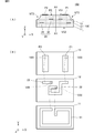
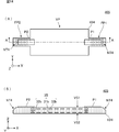
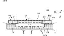
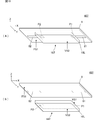
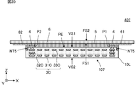
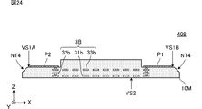
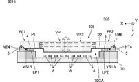
La présente invention concerne un composant électronique (101) comprenant un substrat isolant (10) ayant une première surface principale (VS1) qui sert de surface de montage, une bobine qui est formée sur le substrat isolant (3), et des électrodes de montage (P1, P2) qui sont connectées à la bobine (3) formée sur la première surface principale (VS1) Le substrat isolant (10) est formé par stratification d'une pluralité de couches de substrat isolant (11, 12, 13). La bobine (3) est conçue avec un conducteur de bobine (31) formé dans le substrat isolant (12), et a un axe d'enroulement (AX) dans la direction de stratification (la direction de l'axe z) de la pluralité de couches de substrat isolant (11, 12, 13). La surface de la première surface principale (VS1) diffère de la surface de la première surface principale (VS1) dans une section transversale parallèle à la première surface principale (VS1) (la section transversale du plan XY), et est plus petite que la surface de la section transversale la plus proche de la première surface principale (VS1) (par exemple, l'interface entre la couche de substrat isolant (12) et la couche de substrat isolant (13)).
Priority Applications (2)
| Application Number | Priority Date | Filing Date | Title |
|---|---|---|---|
| CN201790000966.2U CN209729659U (zh) | 2016-06-17 | 2017-06-08 | 电子部件、振动板以及电子设备 |
| US16/195,917 US10770215B2 (en) | 2016-06-17 | 2018-11-20 | Electronic component, diaphragm, electronic device, and electronic component manufacturing method |
Applications Claiming Priority (4)
| Application Number | Priority Date | Filing Date | Title |
|---|---|---|---|
| JP2016120892 | 2016-06-17 | ||
| JP2016-120892 | 2016-06-17 | ||
| JP2017-033470 | 2017-02-24 | ||
| JP2017033470 | 2017-02-24 |
Related Child Applications (1)
| Application Number | Title | Priority Date | Filing Date |
|---|---|---|---|
| US16/195,917 Continuation US10770215B2 (en) | 2016-06-17 | 2018-11-20 | Electronic component, diaphragm, electronic device, and electronic component manufacturing method |
Publications (1)
| Publication Number | Publication Date |
|---|---|
| WO2017217308A1 true WO2017217308A1 (fr) | 2017-12-21 |
Family
ID=60664452
Family Applications (1)
| Application Number | Title | Priority Date | Filing Date |
|---|---|---|---|
| PCT/JP2017/021254 WO2017217308A1 (fr) | 2016-06-17 | 2017-06-08 | Composant électronique, plaque vibrante, dispositif électronique et procédé de fabrication de composants électroniques |
Country Status (3)
| Country | Link |
|---|---|
| US (1) | US10770215B2 (fr) |
| CN (1) | CN209729659U (fr) |
| WO (1) | WO2017217308A1 (fr) |
Cited By (3)
| Publication number | Priority date | Publication date | Assignee | Title |
|---|---|---|---|---|
| FR3082046A1 (fr) * | 2018-05-30 | 2019-12-06 | Commissariat A L'energie Atomique Et Aux Energies Alternatives | Circuit integre comportant une inductance |
| JP2020057655A (ja) * | 2018-09-28 | 2020-04-09 | 太陽誘電株式会社 | コイル部品及び電子機器 |
| JP2022071517A (ja) * | 2020-10-28 | 2022-05-16 | 株式会社村田製作所 | インダクタ部品及びインダクタ部品実装基板 |
Families Citing this family (1)
| Publication number | Priority date | Publication date | Assignee | Title |
|---|---|---|---|---|
| KR101973449B1 (ko) * | 2017-12-11 | 2019-04-29 | 삼성전기주식회사 | 인덕터 |
Citations (11)
| Publication number | Priority date | Publication date | Assignee | Title |
|---|---|---|---|---|
| JPS6052668U (ja) * | 1983-09-20 | 1985-04-13 | 株式会社東芝 | チツプ部品 |
| JPH118157A (ja) * | 1997-06-17 | 1999-01-12 | Murata Mfg Co Ltd | 積層電子部品の製造方法 |
| JP2006287924A (ja) * | 2005-03-09 | 2006-10-19 | Furukawa Electric Co Ltd:The | 平面スピーカ用振動板及び平面スピーカ |
| JP2009034694A (ja) * | 2007-07-31 | 2009-02-19 | Disco Abrasive Syst Ltd | レーザ加工方法 |
| JP2010010321A (ja) * | 2008-06-26 | 2010-01-14 | Panasonic Corp | コイル部品の製造方法 |
| JP2011238895A (ja) * | 2010-04-13 | 2011-11-24 | Denso Corp | 半導体装置およびその製造方法 |
| JP2012060013A (ja) * | 2010-09-10 | 2012-03-22 | Kyocera Corp | 電子部品モジュール、電子部品およびその製造方法 |
| JP2013501350A (ja) * | 2009-07-31 | 2013-01-10 | オスラム オプト セミコンダクターズ ゲゼルシャフト ミット ベシュレンクテル ハフツング | 発光ダイオードチップ |
| JP2014517594A (ja) * | 2011-05-11 | 2014-07-17 | エクセルウェイ インク | マルチレイヤpcbパターンボイスコイルフィルムを有する平板状スピーカー |
| WO2015079941A1 (fr) * | 2013-11-28 | 2015-06-04 | 株式会社村田製作所 | Procédé de fabrication d'un substrat multicouche, substrat multicouche, et électroaimant |
| WO2015129601A1 (fr) * | 2014-02-27 | 2015-09-03 | 株式会社村田製作所 | Procédé de fabrication d'électro-aimant, et électro-aimant |
Family Cites Families (2)
| Publication number | Priority date | Publication date | Assignee | Title |
|---|---|---|---|---|
| JPH0766606A (ja) | 1993-08-23 | 1995-03-10 | Murata Mfg Co Ltd | 表面実装型電子部品 |
| CN204808996U (zh) | 2013-01-22 | 2015-11-25 | 株式会社村田制作所 | 线圈元器件及电子设备 |
-
2017
- 2017-06-08 WO PCT/JP2017/021254 patent/WO2017217308A1/fr active Application Filing
- 2017-06-08 CN CN201790000966.2U patent/CN209729659U/zh active Active
-
2018
- 2018-11-20 US US16/195,917 patent/US10770215B2/en active Active
Patent Citations (11)
| Publication number | Priority date | Publication date | Assignee | Title |
|---|---|---|---|---|
| JPS6052668U (ja) * | 1983-09-20 | 1985-04-13 | 株式会社東芝 | チツプ部品 |
| JPH118157A (ja) * | 1997-06-17 | 1999-01-12 | Murata Mfg Co Ltd | 積層電子部品の製造方法 |
| JP2006287924A (ja) * | 2005-03-09 | 2006-10-19 | Furukawa Electric Co Ltd:The | 平面スピーカ用振動板及び平面スピーカ |
| JP2009034694A (ja) * | 2007-07-31 | 2009-02-19 | Disco Abrasive Syst Ltd | レーザ加工方法 |
| JP2010010321A (ja) * | 2008-06-26 | 2010-01-14 | Panasonic Corp | コイル部品の製造方法 |
| JP2013501350A (ja) * | 2009-07-31 | 2013-01-10 | オスラム オプト セミコンダクターズ ゲゼルシャフト ミット ベシュレンクテル ハフツング | 発光ダイオードチップ |
| JP2011238895A (ja) * | 2010-04-13 | 2011-11-24 | Denso Corp | 半導体装置およびその製造方法 |
| JP2012060013A (ja) * | 2010-09-10 | 2012-03-22 | Kyocera Corp | 電子部品モジュール、電子部品およびその製造方法 |
| JP2014517594A (ja) * | 2011-05-11 | 2014-07-17 | エクセルウェイ インク | マルチレイヤpcbパターンボイスコイルフィルムを有する平板状スピーカー |
| WO2015079941A1 (fr) * | 2013-11-28 | 2015-06-04 | 株式会社村田製作所 | Procédé de fabrication d'un substrat multicouche, substrat multicouche, et électroaimant |
| WO2015129601A1 (fr) * | 2014-02-27 | 2015-09-03 | 株式会社村田製作所 | Procédé de fabrication d'électro-aimant, et électro-aimant |
Cited By (7)
| Publication number | Priority date | Publication date | Assignee | Title |
|---|---|---|---|---|
| FR3082046A1 (fr) * | 2018-05-30 | 2019-12-06 | Commissariat A L'energie Atomique Et Aux Energies Alternatives | Circuit integre comportant une inductance |
| EP3579255A1 (fr) | 2018-05-30 | 2019-12-11 | Commissariat à l'Énergie Atomique et aux Énergies Alternatives | Circuit integre comportant une inductance variable |
| US11017940B2 (en) | 2018-05-30 | 2021-05-25 | Commissariat A L'energie Atomique Et Aux Energies Alternatives | Integrated circuit comprising a variable inductor |
| JP2020057655A (ja) * | 2018-09-28 | 2020-04-09 | 太陽誘電株式会社 | コイル部品及び電子機器 |
| JP7193968B2 (ja) | 2018-09-28 | 2022-12-21 | 太陽誘電株式会社 | コイル部品及び電子機器 |
| JP2022071517A (ja) * | 2020-10-28 | 2022-05-16 | 株式会社村田製作所 | インダクタ部品及びインダクタ部品実装基板 |
| JP7294300B2 (ja) | 2020-10-28 | 2023-06-20 | 株式会社村田製作所 | インダクタ部品及びインダクタ部品実装基板 |
Also Published As
| Publication number | Publication date |
|---|---|
| US20190088403A1 (en) | 2019-03-21 |
| CN209729659U (zh) | 2019-12-03 |
| US10770215B2 (en) | 2020-09-08 |
Similar Documents
| Publication | Publication Date | Title |
|---|---|---|
| JP6642708B2 (ja) | 電子部品、振動板および電子機器 | |
| US9947466B2 (en) | Electronic component | |
| WO2017217308A1 (fr) | Composant électronique, plaque vibrante, dispositif électronique et procédé de fabrication de composants électroniques | |
| WO2017018109A1 (fr) | Bobine d'induction flexible | |
| US10051730B2 (en) | Multilayer substrate manufacturing method and multilayer substrate | |
| JP2014038884A (ja) | 電子部品および電子部品の製造方法 | |
| US11540393B2 (en) | Multilayer substrate, multilayer substrate mounting structure, method of manufacturing multilayer substrate, and method of manufacturing electronic device | |
| JPWO2019069637A1 (ja) | インターポーザおよび電子機器 | |
| JP2004040001A (ja) | コイル部品及び回路装置 | |
| JP6673304B2 (ja) | 多層基板 | |
| JP6913155B2 (ja) | アクチュエータ | |
| JP6693707B2 (ja) | 基板集積インターコネクト | |
| WO2019026819A1 (fr) | Actionneur | |
| US11043626B2 (en) | Multilayer substrate | |
| JP6863230B2 (ja) | 回路素子および電子機器 | |
| WO2018105392A1 (fr) | Élément de vibration | |
| CN111599569B (zh) | 线圈部件 | |
| JP2010141029A (ja) | プリント配線板及びその製造方法 | |
| JP6673162B2 (ja) | 振動素子および振動板 | |
| JP2009049325A (ja) | 電子部品モジュール及びその製造方法 | |
| WO2019240000A1 (fr) | Procédé de fabrication d'élément électrique, élément électrique et structure de montage d'élément électrique | |
| JP2023038612A (ja) | コイル部品 | |
| WO2017145505A1 (fr) | Dispositif à ci sans fil et procédé de fabrication de dispositif à ci sans fil | |
| JP2019083239A (ja) | 電子機器 |
Legal Events
| Date | Code | Title | Description |
|---|---|---|---|
| 121 | Ep: the epo has been informed by wipo that ep was designated in this application |
Ref document number: 17813206 Country of ref document: EP Kind code of ref document: A1 |
|
| NENP | Non-entry into the national phase |
Ref country code: DE |
|
| 122 | Ep: pct application non-entry in european phase |
Ref document number: 17813206 Country of ref document: EP Kind code of ref document: A1 |
|
| NENP | Non-entry into the national phase |
Ref country code: JP |